EP2277197B1 - Method for constructing an electronic module - Google Patents
Method for constructing an electronic moduleDownload PDFInfo
- Publication number
- EP2277197B1 EP2277197B1EP09727616.6AEP09727616AEP2277197B1EP 2277197 B1EP2277197 B1EP 2277197B1EP 09727616 AEP09727616 AEP 09727616AEP 2277197 B1EP2277197 B1EP 2277197B1
- Authority
- EP
- European Patent Office
- Prior art keywords
- substrate
- approximately
- die
- cavity
- post
- Prior art date
- Legal status (The legal status is an assumption and is not a legal conclusion. Google has not performed a legal analysis and makes no representation as to the accuracy of the status listed.)
- Not-in-force
Links
Images


Classifications
- H—ELECTRICITY
- H01—ELECTRIC ELEMENTS
- H01L—SEMICONDUCTOR DEVICES NOT COVERED BY CLASS H10
- H01L21/00—Processes or apparatus adapted for the manufacture or treatment of semiconductor or solid state devices or of parts thereof
- H01L21/02—Manufacture or treatment of semiconductor devices or of parts thereof
- H01L21/04—Manufacture or treatment of semiconductor devices or of parts thereof the devices having potential barriers, e.g. a PN junction, depletion layer or carrier concentration layer
- H01L21/48—Manufacture or treatment of parts, e.g. containers, prior to assembly of the devices, using processes not provided for in a single one of the groups H01L21/18 - H01L21/326 or H10D48/04 - H10D48/07
- H01L21/4814—Conductive parts
- H01L21/4846—Leads on or in insulating or insulated substrates, e.g. metallisation
- H01L21/486—Via connections through the substrate with or without pins
- B—PERFORMING OPERATIONS; TRANSPORTING
- B81—MICROSTRUCTURAL TECHNOLOGY
- B81C—PROCESSES OR APPARATUS SPECIALLY ADAPTED FOR THE MANUFACTURE OR TREATMENT OF MICROSTRUCTURAL DEVICES OR SYSTEMS
- B81C1/00—Manufacture or treatment of devices or systems in or on a substrate
- B81C1/00015—Manufacture or treatment of devices or systems in or on a substrate for manufacturing microsystems
- B81C1/00261—Processes for packaging MEMS devices
- B81C1/00333—Aspects relating to packaging of MEMS devices, not covered by groups B81C1/00269 - B81C1/00325
- H—ELECTRICITY
- H01—ELECTRIC ELEMENTS
- H01L—SEMICONDUCTOR DEVICES NOT COVERED BY CLASS H10
- H01L21/00—Processes or apparatus adapted for the manufacture or treatment of semiconductor or solid state devices or of parts thereof
- H01L21/67—Apparatus specially adapted for handling semiconductor or electric solid state devices during manufacture or treatment thereof; Apparatus specially adapted for handling wafers during manufacture or treatment of semiconductor or electric solid state devices or components ; Apparatus not specifically provided for elsewhere
- H01L21/683—Apparatus specially adapted for handling semiconductor or electric solid state devices during manufacture or treatment thereof; Apparatus specially adapted for handling wafers during manufacture or treatment of semiconductor or electric solid state devices or components ; Apparatus not specifically provided for elsewhere for supporting or gripping
- H01L21/6835—Apparatus specially adapted for handling semiconductor or electric solid state devices during manufacture or treatment thereof; Apparatus specially adapted for handling wafers during manufacture or treatment of semiconductor or electric solid state devices or components ; Apparatus not specifically provided for elsewhere for supporting or gripping using temporarily an auxiliary support
- H—ELECTRICITY
- H01—ELECTRIC ELEMENTS
- H01L—SEMICONDUCTOR DEVICES NOT COVERED BY CLASS H10
- H01L23/00—Details of semiconductor or other solid state devices
- H01L23/12—Mountings, e.g. non-detachable insulating substrates
- H01L23/13—Mountings, e.g. non-detachable insulating substrates characterised by the shape
- H—ELECTRICITY
- H01—ELECTRIC ELEMENTS
- H01L—SEMICONDUCTOR DEVICES NOT COVERED BY CLASS H10
- H01L24/00—Arrangements for connecting or disconnecting semiconductor or solid-state bodies; Methods or apparatus related thereto
- H01L24/01—Means for bonding being attached to, or being formed on, the surface to be connected, e.g. chip-to-package, die-attach, "first-level" interconnects; Manufacturing methods related thereto
- H01L24/18—High density interconnect [HDI] connectors; Manufacturing methods related thereto
- H01L24/23—Structure, shape, material or disposition of the high density interconnect connectors after the connecting process
- H01L24/24—Structure, shape, material or disposition of the high density interconnect connectors after the connecting process of an individual high density interconnect connector
- H—ELECTRICITY
- H01—ELECTRIC ELEMENTS
- H01L—SEMICONDUCTOR DEVICES NOT COVERED BY CLASS H10
- H01L24/00—Arrangements for connecting or disconnecting semiconductor or solid-state bodies; Methods or apparatus related thereto
- H01L24/80—Methods for connecting semiconductor or other solid state bodies using means for bonding being attached to, or being formed on, the surface to be connected
- H01L24/82—Methods for connecting semiconductor or other solid state bodies using means for bonding being attached to, or being formed on, the surface to be connected by forming build-up interconnects at chip-level, e.g. for high density interconnects [HDI]
- H—ELECTRICITY
- H01—ELECTRIC ELEMENTS
- H01L—SEMICONDUCTOR DEVICES NOT COVERED BY CLASS H10
- H01L25/00—Assemblies consisting of a plurality of semiconductor or other solid state devices
- H01L25/03—Assemblies consisting of a plurality of semiconductor or other solid state devices all the devices being of a type provided for in a single subclass of subclasses H10B, H10D, H10F, H10H, H10K or H10N, e.g. assemblies of rectifier diodes
- H01L25/10—Assemblies consisting of a plurality of semiconductor or other solid state devices all the devices being of a type provided for in a single subclass of subclasses H10B, H10D, H10F, H10H, H10K or H10N, e.g. assemblies of rectifier diodes the devices having separate containers
- H01L25/105—Assemblies consisting of a plurality of semiconductor or other solid state devices all the devices being of a type provided for in a single subclass of subclasses H10B, H10D, H10F, H10H, H10K or H10N, e.g. assemblies of rectifier diodes the devices having separate containers the devices being integrated devices of class H10
- B—PERFORMING OPERATIONS; TRANSPORTING
- B81—MICROSTRUCTURAL TECHNOLOGY
- B81B—MICROSTRUCTURAL DEVICES OR SYSTEMS, e.g. MICROMECHANICAL DEVICES
- B81B2207/00—Microstructural systems or auxiliary parts thereof
- B81B2207/01—Microstructural systems or auxiliary parts thereof comprising a micromechanical device connected to control or processing electronics, i.e. Smart-MEMS
- B81B2207/012—Microstructural systems or auxiliary parts thereof comprising a micromechanical device connected to control or processing electronics, i.e. Smart-MEMS the micromechanical device and the control or processing electronics being separate parts in the same package
- B—PERFORMING OPERATIONS; TRANSPORTING
- B81—MICROSTRUCTURAL TECHNOLOGY
- B81C—PROCESSES OR APPARATUS SPECIALLY ADAPTED FOR THE MANUFACTURE OR TREATMENT OF MICROSTRUCTURAL DEVICES OR SYSTEMS
- B81C2201/00—Manufacture or treatment of microstructural devices or systems
- B81C2201/01—Manufacture or treatment of microstructural devices or systems in or on a substrate
- B81C2201/0174—Manufacture or treatment of microstructural devices or systems in or on a substrate for making multi-layered devices, film deposition or growing
- B81C2201/019—Bonding or gluing multiple substrate layers
- B—PERFORMING OPERATIONS; TRANSPORTING
- B81—MICROSTRUCTURAL TECHNOLOGY
- B81C—PROCESSES OR APPARATUS SPECIALLY ADAPTED FOR THE MANUFACTURE OR TREATMENT OF MICROSTRUCTURAL DEVICES OR SYSTEMS
- B81C2201/00—Manufacture or treatment of microstructural devices or systems
- B81C2201/01—Manufacture or treatment of microstructural devices or systems in or on a substrate
- B81C2201/0174—Manufacture or treatment of microstructural devices or systems in or on a substrate for making multi-layered devices, film deposition or growing
- B81C2201/0191—Transfer of a layer from a carrier wafer to a device wafer
- H—ELECTRICITY
- H01—ELECTRIC ELEMENTS
- H01L—SEMICONDUCTOR DEVICES NOT COVERED BY CLASS H10
- H01L21/00—Processes or apparatus adapted for the manufacture or treatment of semiconductor or solid state devices or of parts thereof
- H01L21/02—Manufacture or treatment of semiconductor devices or of parts thereof
- H01L21/04—Manufacture or treatment of semiconductor devices or of parts thereof the devices having potential barriers, e.g. a PN junction, depletion layer or carrier concentration layer
- H01L21/50—Assembly of semiconductor devices using processes or apparatus not provided for in a single one of the groups H01L21/18 - H01L21/326 or H10D48/04 - H10D48/07 e.g. sealing of a cap to a base of a container
- H01L21/56—Encapsulations, e.g. encapsulation layers, coatings
- H01L21/568—Temporary substrate used as encapsulation process aid
- H—ELECTRICITY
- H01—ELECTRIC ELEMENTS
- H01L—SEMICONDUCTOR DEVICES NOT COVERED BY CLASS H10
- H01L2221/00—Processes or apparatus adapted for the manufacture or treatment of semiconductor or solid state devices or of parts thereof covered by H01L21/00
- H01L2221/67—Apparatus for handling semiconductor or electric solid state devices during manufacture or treatment thereof; Apparatus for handling wafers during manufacture or treatment of semiconductor or electric solid state devices or components; Apparatus not specifically provided for elsewhere
- H01L2221/683—Apparatus for handling semiconductor or electric solid state devices during manufacture or treatment thereof; Apparatus for handling wafers during manufacture or treatment of semiconductor or electric solid state devices or components; Apparatus not specifically provided for elsewhere for supporting or gripping
- H01L2221/68304—Apparatus for handling semiconductor or electric solid state devices during manufacture or treatment thereof; Apparatus for handling wafers during manufacture or treatment of semiconductor or electric solid state devices or components; Apparatus not specifically provided for elsewhere for supporting or gripping using temporarily an auxiliary support
- H01L2221/68359—Apparatus for handling semiconductor or electric solid state devices during manufacture or treatment thereof; Apparatus for handling wafers during manufacture or treatment of semiconductor or electric solid state devices or components; Apparatus not specifically provided for elsewhere for supporting or gripping using temporarily an auxiliary support used as a support during manufacture of interconnect decals or build up layers
- H—ELECTRICITY
- H01—ELECTRIC ELEMENTS
- H01L—SEMICONDUCTOR DEVICES NOT COVERED BY CLASS H10
- H01L2221/00—Processes or apparatus adapted for the manufacture or treatment of semiconductor or solid state devices or of parts thereof covered by H01L21/00
- H01L2221/67—Apparatus for handling semiconductor or electric solid state devices during manufacture or treatment thereof; Apparatus for handling wafers during manufacture or treatment of semiconductor or electric solid state devices or components; Apparatus not specifically provided for elsewhere
- H01L2221/683—Apparatus for handling semiconductor or electric solid state devices during manufacture or treatment thereof; Apparatus for handling wafers during manufacture or treatment of semiconductor or electric solid state devices or components; Apparatus not specifically provided for elsewhere for supporting or gripping
- H01L2221/68304—Apparatus for handling semiconductor or electric solid state devices during manufacture or treatment thereof; Apparatus for handling wafers during manufacture or treatment of semiconductor or electric solid state devices or components; Apparatus not specifically provided for elsewhere for supporting or gripping using temporarily an auxiliary support
- H01L2221/68377—Apparatus for handling semiconductor or electric solid state devices during manufacture or treatment thereof; Apparatus for handling wafers during manufacture or treatment of semiconductor or electric solid state devices or components; Apparatus not specifically provided for elsewhere for supporting or gripping using temporarily an auxiliary support with parts of the auxiliary support remaining in the finished device
- H—ELECTRICITY
- H01—ELECTRIC ELEMENTS
- H01L—SEMICONDUCTOR DEVICES NOT COVERED BY CLASS H10
- H01L2224/00—Indexing scheme for arrangements for connecting or disconnecting semiconductor or solid-state bodies and methods related thereto as covered by H01L24/00
- H01L2224/01—Means for bonding being attached to, or being formed on, the surface to be connected, e.g. chip-to-package, die-attach, "first-level" interconnects; Manufacturing methods related thereto
- H01L2224/02—Bonding areas; Manufacturing methods related thereto
- H01L2224/04—Structure, shape, material or disposition of the bonding areas prior to the connecting process
- H01L2224/04105—Bonding areas formed on an encapsulation of the semiconductor or solid-state body, e.g. bonding areas on chip-scale packages
- H—ELECTRICITY
- H01—ELECTRIC ELEMENTS
- H01L—SEMICONDUCTOR DEVICES NOT COVERED BY CLASS H10
- H01L2224/00—Indexing scheme for arrangements for connecting or disconnecting semiconductor or solid-state bodies and methods related thereto as covered by H01L24/00
- H01L2224/01—Means for bonding being attached to, or being formed on, the surface to be connected, e.g. chip-to-package, die-attach, "first-level" interconnects; Manufacturing methods related thereto
- H01L2224/18—High density interconnect [HDI] connectors; Manufacturing methods related thereto
- H01L2224/23—Structure, shape, material or disposition of the high density interconnect connectors after the connecting process
- H01L2224/24—Structure, shape, material or disposition of the high density interconnect connectors after the connecting process of an individual high density interconnect connector
- H01L2224/241—Disposition
- H01L2224/24151—Connecting between a semiconductor or solid-state body and an item not being a semiconductor or solid-state body, e.g. chip-to-substrate, chip-to-passive
- H01L2224/24221—Connecting between a semiconductor or solid-state body and an item not being a semiconductor or solid-state body, e.g. chip-to-substrate, chip-to-passive the body and the item being stacked
- H01L2224/24225—Connecting between a semiconductor or solid-state body and an item not being a semiconductor or solid-state body, e.g. chip-to-substrate, chip-to-passive the body and the item being stacked the item being non-metallic, e.g. insulating substrate with or without metallisation
- H01L2224/24227—Connecting between a semiconductor or solid-state body and an item not being a semiconductor or solid-state body, e.g. chip-to-substrate, chip-to-passive the body and the item being stacked the item being non-metallic, e.g. insulating substrate with or without metallisation the HDI interconnect not connecting to the same level of the item at which the semiconductor or solid-state body is mounted, e.g. the semiconductor or solid-state body being mounted in a cavity or on a protrusion of the item
- H—ELECTRICITY
- H01—ELECTRIC ELEMENTS
- H01L—SEMICONDUCTOR DEVICES NOT COVERED BY CLASS H10
- H01L2224/00—Indexing scheme for arrangements for connecting or disconnecting semiconductor or solid-state bodies and methods related thereto as covered by H01L24/00
- H01L2224/73—Means for bonding being of different types provided for in two or more of groups H01L2224/10, H01L2224/18, H01L2224/26, H01L2224/34, H01L2224/42, H01L2224/50, H01L2224/63, H01L2224/71
- H01L2224/732—Location after the connecting process
- H01L2224/73251—Location after the connecting process on different surfaces
- H01L2224/73267—Layer and HDI connectors
- H—ELECTRICITY
- H01—ELECTRIC ELEMENTS
- H01L—SEMICONDUCTOR DEVICES NOT COVERED BY CLASS H10
- H01L2224/00—Indexing scheme for arrangements for connecting or disconnecting semiconductor or solid-state bodies and methods related thereto as covered by H01L24/00
- H01L2224/80—Methods for connecting semiconductor or other solid state bodies using means for bonding being attached to, or being formed on, the surface to be connected
- H01L2224/82—Methods for connecting semiconductor or other solid state bodies using means for bonding being attached to, or being formed on, the surface to be connected by forming build-up interconnects at chip-level, e.g. for high density interconnects [HDI]
- H01L2224/82009—Pre-treatment of the connector or the bonding area
- H01L2224/8203—Reshaping, e.g. forming vias
- H—ELECTRICITY
- H01—ELECTRIC ELEMENTS
- H01L—SEMICONDUCTOR DEVICES NOT COVERED BY CLASS H10
- H01L2224/00—Indexing scheme for arrangements for connecting or disconnecting semiconductor or solid-state bodies and methods related thereto as covered by H01L24/00
- H01L2224/91—Methods for connecting semiconductor or solid state bodies including different methods provided for in two or more of groups H01L2224/80 - H01L2224/90
- H01L2224/92—Specific sequence of method steps
- H01L2224/921—Connecting a surface with connectors of different types
- H01L2224/9212—Sequential connecting processes
- H01L2224/92142—Sequential connecting processes the first connecting process involving a layer connector
- H01L2224/92144—Sequential connecting processes the first connecting process involving a layer connector the second connecting process involving a build-up interconnect
- H—ELECTRICITY
- H01—ELECTRIC ELEMENTS
- H01L—SEMICONDUCTOR DEVICES NOT COVERED BY CLASS H10
- H01L2224/00—Indexing scheme for arrangements for connecting or disconnecting semiconductor or solid-state bodies and methods related thereto as covered by H01L24/00
- H01L2224/91—Methods for connecting semiconductor or solid state bodies including different methods provided for in two or more of groups H01L2224/80 - H01L2224/90
- H01L2224/92—Specific sequence of method steps
- H01L2224/922—Connecting different surfaces of the semiconductor or solid-state body with connectors of different types
- H01L2224/9222—Sequential connecting processes
- H—ELECTRICITY
- H01—ELECTRIC ELEMENTS
- H01L—SEMICONDUCTOR DEVICES NOT COVERED BY CLASS H10
- H01L2225/00—Details relating to assemblies covered by the group H01L25/00 but not provided for in its subgroups
- H01L2225/03—All the devices being of a type provided for in the same main group of the same subclass of class H10, e.g. assemblies of rectifier diodes
- H01L2225/10—All the devices being of a type provided for in the same main group of the same subclass of class H10, e.g. assemblies of rectifier diodes the devices having separate containers
- H01L2225/1005—All the devices being of a type provided for in the same main group of the same subclass of class H10, e.g. assemblies of rectifier diodes the devices having separate containers the devices being integrated devices of class H10
- H01L2225/1011—All the devices being of a type provided for in the same main group of the same subclass of class H10, e.g. assemblies of rectifier diodes the devices having separate containers the devices being integrated devices of class H10 the containers being in a stacked arrangement
- H01L2225/1017—All the devices being of a type provided for in the same main group of the same subclass of class H10, e.g. assemblies of rectifier diodes the devices having separate containers the devices being integrated devices of class H10 the containers being in a stacked arrangement the lowermost container comprising a device support
- H01L2225/1035—All the devices being of a type provided for in the same main group of the same subclass of class H10, e.g. assemblies of rectifier diodes the devices having separate containers the devices being integrated devices of class H10 the containers being in a stacked arrangement the lowermost container comprising a device support the device being entirely enclosed by the support, e.g. high-density interconnect [HDI]
- H—ELECTRICITY
- H01—ELECTRIC ELEMENTS
- H01L—SEMICONDUCTOR DEVICES NOT COVERED BY CLASS H10
- H01L2225/00—Details relating to assemblies covered by the group H01L25/00 but not provided for in its subgroups
- H01L2225/03—All the devices being of a type provided for in the same main group of the same subclass of class H10, e.g. assemblies of rectifier diodes
- H01L2225/10—All the devices being of a type provided for in the same main group of the same subclass of class H10, e.g. assemblies of rectifier diodes the devices having separate containers
- H01L2225/1005—All the devices being of a type provided for in the same main group of the same subclass of class H10, e.g. assemblies of rectifier diodes the devices having separate containers the devices being integrated devices of class H10
- H01L2225/1011—All the devices being of a type provided for in the same main group of the same subclass of class H10, e.g. assemblies of rectifier diodes the devices having separate containers the devices being integrated devices of class H10 the containers being in a stacked arrangement
- H01L2225/1047—Details of electrical connections between containers
- H01L2225/1058—Bump or bump-like electrical connections, e.g. balls, pillars, posts
- H—ELECTRICITY
- H01—ELECTRIC ELEMENTS
- H01L—SEMICONDUCTOR DEVICES NOT COVERED BY CLASS H10
- H01L23/00—Details of semiconductor or other solid state devices
- H01L23/48—Arrangements for conducting electric current to or from the solid state body in operation, e.g. leads, terminal arrangements ; Selection of materials therefor
- H01L23/488—Arrangements for conducting electric current to or from the solid state body in operation, e.g. leads, terminal arrangements ; Selection of materials therefor consisting of soldered or bonded constructions
- H01L23/498—Leads, i.e. metallisations or lead-frames on insulating substrates, e.g. chip carriers
- H01L23/49827—Via connections through the substrates, e.g. pins going through the substrate, coaxial cables
- H—ELECTRICITY
- H01—ELECTRIC ELEMENTS
- H01L—SEMICONDUCTOR DEVICES NOT COVERED BY CLASS H10
- H01L24/00—Arrangements for connecting or disconnecting semiconductor or solid-state bodies; Methods or apparatus related thereto
- H01L24/01—Means for bonding being attached to, or being formed on, the surface to be connected, e.g. chip-to-package, die-attach, "first-level" interconnects; Manufacturing methods related thereto
- H01L24/18—High density interconnect [HDI] connectors; Manufacturing methods related thereto
- H01L24/19—Manufacturing methods of high density interconnect preforms
- H—ELECTRICITY
- H01—ELECTRIC ELEMENTS
- H01L—SEMICONDUCTOR DEVICES NOT COVERED BY CLASS H10
- H01L2924/00—Indexing scheme for arrangements or methods for connecting or disconnecting semiconductor or solid-state bodies as covered by H01L24/00
- H01L2924/01—Chemical elements
- H01L2924/01006—Carbon [C]
- H—ELECTRICITY
- H01—ELECTRIC ELEMENTS
- H01L—SEMICONDUCTOR DEVICES NOT COVERED BY CLASS H10
- H01L2924/00—Indexing scheme for arrangements or methods for connecting or disconnecting semiconductor or solid-state bodies as covered by H01L24/00
- H01L2924/01—Chemical elements
- H01L2924/01015—Phosphorus [P]
- H—ELECTRICITY
- H01—ELECTRIC ELEMENTS
- H01L—SEMICONDUCTOR DEVICES NOT COVERED BY CLASS H10
- H01L2924/00—Indexing scheme for arrangements or methods for connecting or disconnecting semiconductor or solid-state bodies as covered by H01L24/00
- H01L2924/01—Chemical elements
- H01L2924/01019—Potassium [K]
- H—ELECTRICITY
- H01—ELECTRIC ELEMENTS
- H01L—SEMICONDUCTOR DEVICES NOT COVERED BY CLASS H10
- H01L2924/00—Indexing scheme for arrangements or methods for connecting or disconnecting semiconductor or solid-state bodies as covered by H01L24/00
- H01L2924/01—Chemical elements
- H01L2924/01029—Copper [Cu]
- H—ELECTRICITY
- H01—ELECTRIC ELEMENTS
- H01L—SEMICONDUCTOR DEVICES NOT COVERED BY CLASS H10
- H01L2924/00—Indexing scheme for arrangements or methods for connecting or disconnecting semiconductor or solid-state bodies as covered by H01L24/00
- H01L2924/01—Chemical elements
- H01L2924/01033—Arsenic [As]
- H—ELECTRICITY
- H01—ELECTRIC ELEMENTS
- H01L—SEMICONDUCTOR DEVICES NOT COVERED BY CLASS H10
- H01L2924/00—Indexing scheme for arrangements or methods for connecting or disconnecting semiconductor or solid-state bodies as covered by H01L24/00
- H01L2924/01—Chemical elements
- H01L2924/01042—Molybdenum [Mo]
- H—ELECTRICITY
- H01—ELECTRIC ELEMENTS
- H01L—SEMICONDUCTOR DEVICES NOT COVERED BY CLASS H10
- H01L2924/00—Indexing scheme for arrangements or methods for connecting or disconnecting semiconductor or solid-state bodies as covered by H01L24/00
- H01L2924/01—Chemical elements
- H01L2924/01074—Tungsten [W]
- H—ELECTRICITY
- H01—ELECTRIC ELEMENTS
- H01L—SEMICONDUCTOR DEVICES NOT COVERED BY CLASS H10
- H01L2924/00—Indexing scheme for arrangements or methods for connecting or disconnecting semiconductor or solid-state bodies as covered by H01L24/00
- H01L2924/01—Chemical elements
- H01L2924/01084—Polonium [Po]
- H—ELECTRICITY
- H01—ELECTRIC ELEMENTS
- H01L—SEMICONDUCTOR DEVICES NOT COVERED BY CLASS H10
- H01L2924/00—Indexing scheme for arrangements or methods for connecting or disconnecting semiconductor or solid-state bodies as covered by H01L24/00
- H01L2924/013—Alloys
- H01L2924/014—Solder alloys
- H—ELECTRICITY
- H01—ELECTRIC ELEMENTS
- H01L—SEMICONDUCTOR DEVICES NOT COVERED BY CLASS H10
- H01L2924/00—Indexing scheme for arrangements or methods for connecting or disconnecting semiconductor or solid-state bodies as covered by H01L24/00
- H01L2924/10—Details of semiconductor or other solid state devices to be connected
- H01L2924/102—Material of the semiconductor or solid state bodies
- H01L2924/1025—Semiconducting materials
- H01L2924/1026—Compound semiconductors
- H01L2924/1032—III-V
- H01L2924/10329—Gallium arsenide [GaAs]
- H—ELECTRICITY
- H01—ELECTRIC ELEMENTS
- H01L—SEMICONDUCTOR DEVICES NOT COVERED BY CLASS H10
- H01L2924/00—Indexing scheme for arrangements or methods for connecting or disconnecting semiconductor or solid-state bodies as covered by H01L24/00
- H01L2924/10—Details of semiconductor or other solid state devices to be connected
- H01L2924/11—Device type
- H01L2924/12—Passive devices, e.g. 2 terminal devices
- H01L2924/1204—Optical Diode
- H01L2924/12042—LASER
- H—ELECTRICITY
- H01—ELECTRIC ELEMENTS
- H01L—SEMICONDUCTOR DEVICES NOT COVERED BY CLASS H10
- H01L2924/00—Indexing scheme for arrangements or methods for connecting or disconnecting semiconductor or solid-state bodies as covered by H01L24/00
- H01L2924/10—Details of semiconductor or other solid state devices to be connected
- H01L2924/11—Device type
- H01L2924/14—Integrated circuits
- H01L2924/143—Digital devices
- H01L2924/1433—Application-specific integrated circuit [ASIC]
- H—ELECTRICITY
- H01—ELECTRIC ELEMENTS
- H01L—SEMICONDUCTOR DEVICES NOT COVERED BY CLASS H10
- H01L2924/00—Indexing scheme for arrangements or methods for connecting or disconnecting semiconductor or solid-state bodies as covered by H01L24/00
- H01L2924/10—Details of semiconductor or other solid state devices to be connected
- H01L2924/146—Mixed devices
- H01L2924/1461—MEMS
- H—ELECTRICITY
- H01—ELECTRIC ELEMENTS
- H01L—SEMICONDUCTOR DEVICES NOT COVERED BY CLASS H10
- H01L2924/00—Indexing scheme for arrangements or methods for connecting or disconnecting semiconductor or solid-state bodies as covered by H01L24/00
- H01L2924/15—Details of package parts other than the semiconductor or other solid state devices to be connected
- H01L2924/151—Die mounting substrate
- H01L2924/1515—Shape
- H01L2924/15151—Shape the die mounting substrate comprising an aperture, e.g. for underfilling, outgassing, window type wire connections
- H—ELECTRICITY
- H01—ELECTRIC ELEMENTS
- H01L—SEMICONDUCTOR DEVICES NOT COVERED BY CLASS H10
- H01L2924/00—Indexing scheme for arrangements or methods for connecting or disconnecting semiconductor or solid-state bodies as covered by H01L24/00
- H01L2924/15—Details of package parts other than the semiconductor or other solid state devices to be connected
- H01L2924/151—Die mounting substrate
- H01L2924/1515—Shape
- H01L2924/15153—Shape the die mounting substrate comprising a recess for hosting the device
- H—ELECTRICITY
- H01—ELECTRIC ELEMENTS
- H01L—SEMICONDUCTOR DEVICES NOT COVERED BY CLASS H10
- H01L2924/00—Indexing scheme for arrangements or methods for connecting or disconnecting semiconductor or solid-state bodies as covered by H01L24/00
- H01L2924/15—Details of package parts other than the semiconductor or other solid state devices to be connected
- H01L2924/181—Encapsulation
- H01L2924/1815—Shape
- H01L2924/1816—Exposing the passive side of the semiconductor or solid-state body
- H01L2924/18162—Exposing the passive side of the semiconductor or solid-state body of a chip with build-up interconnect
- H—ELECTRICITY
- H01—ELECTRIC ELEMENTS
- H01L—SEMICONDUCTOR DEVICES NOT COVERED BY CLASS H10
- H01L2924/00—Indexing scheme for arrangements or methods for connecting or disconnecting semiconductor or solid-state bodies as covered by H01L24/00
- H01L2924/19—Details of hybrid assemblies other than the semiconductor or other solid state devices to be connected
- H01L2924/1901—Structure
- H01L2924/1904—Component type
- H01L2924/19041—Component type being a capacitor
- H—ELECTRICITY
- H01—ELECTRIC ELEMENTS
- H01L—SEMICONDUCTOR DEVICES NOT COVERED BY CLASS H10
- H01L2924/00—Indexing scheme for arrangements or methods for connecting or disconnecting semiconductor or solid-state bodies as covered by H01L24/00
- H01L2924/19—Details of hybrid assemblies other than the semiconductor or other solid state devices to be connected
- H01L2924/1901—Structure
- H01L2924/1904—Component type
- H01L2924/19042—Component type being an inductor
- H—ELECTRICITY
- H01—ELECTRIC ELEMENTS
- H01L—SEMICONDUCTOR DEVICES NOT COVERED BY CLASS H10
- H01L2924/00—Indexing scheme for arrangements or methods for connecting or disconnecting semiconductor or solid-state bodies as covered by H01L24/00
- H01L2924/19—Details of hybrid assemblies other than the semiconductor or other solid state devices to be connected
- H01L2924/1901—Structure
- H01L2924/1904—Component type
- H01L2924/19043—Component type being a resistor
- Y—GENERAL TAGGING OF NEW TECHNOLOGICAL DEVELOPMENTS; GENERAL TAGGING OF CROSS-SECTIONAL TECHNOLOGIES SPANNING OVER SEVERAL SECTIONS OF THE IPC; TECHNICAL SUBJECTS COVERED BY FORMER USPC CROSS-REFERENCE ART COLLECTIONS [XRACs] AND DIGESTS
- Y10—TECHNICAL SUBJECTS COVERED BY FORMER USPC
- Y10T—TECHNICAL SUBJECTS COVERED BY FORMER US CLASSIFICATION
- Y10T29/00—Metal working
- Y10T29/49—Method of mechanical manufacture
- Y10T29/49002—Electrical device making
- Y10T29/49117—Conductor or circuit manufacturing
- Y10T29/49124—On flat or curved insulated base, e.g., printed circuit, etc.
Definitions
- the present inventionrelates, in various embodiments, to the construction and fabrication of high-density heterogeneous electronic modules and electrical and/or thermal interposers.
- High-density electronic moduleshave been designed and fabricated to satisfy the increasing demand for high levels of functionality in small packages.
- Products that may be made from the modulesinclude memory, digital logic, processing devices, and analog and RF circuits.
- the integration density of electronic modulesis many times greater than surface mount technology ("SMT") is capable of achieving, but less than an application specific integrated circuit (“ASIC").
- SMTsurface mount technology
- ASICapplication specific integrated circuit
- modulesoffer an alternative to ASIC devices, as they require less set-up cost and development time.
- modulesmay be optimized for particular applications that demand multiple functions - for example, a pre-fabricated microelectronic die optimum for each desired function is selected, and the multiple dies are then interconnected and packaged together to form the module.
- the pre-fabricated dieswill have different form factors and thicknesses, making attempts to package them together in a single module problematic. Additional difficulties may arise when attempting to vertically interconnect different layers of dies together in a single module, as the requisite processing may damage the dies in each layer.
- the fabrication of electronic modulestypically features pre-thinned microelectronic dies simply positioned on an adhesive-coated substrate.
- a custom-machined spaceris then placed over and between the dies in order to provide a planar surface for further processing, including metal deposition, patterning, and interconnection.
- a thin dielectric layeris often laminated (via application of high pressure) over the dies and spacer to provide the requisite isolation between the dies and the metal interconnects.
- Vias to the die padsi.e., the conductive contact pads connecting to the inner circuitry of the die
- the dies that are usedtypically cannot be thinned after they are placed on the module substrate, limiting the module thicknesses that may be achieved.
- Another limitation of this methodis the use of laser-drilled vias, which are typically limited in diameter to approximately 40 ⁇ m. This puts constraints on die pad sizes, which restricts design choices to certain devices.
- spacing between diesmust typically be greater than the via diameter to allow deep via formation.
- deep, high-aspect-ratio viasare often difficult to reliably and repeatably fill with the conductive material (as is required to interconnect multiple layers in a module).
- a modulemay have electrical contacts that do not line up, or have a different pitch than, contacts on a circuit board.
- Time-consuming and expensive custom fabrication processesmay be required in order to fabricate connectable parts.
- thermal management solutionssuch as heat sinks, to high-density electronic modules or other electronic components.
- US 5,766,986describes a method and structure having a substrate with a fill hole formed in a first side of the substrate and a cavity formed in a second side of the substrate. An electronic device is positioned in the cavity, which open on the second side of the substrate.
- US 2007/0254411discloses a printed wiring board with an array of electrical contacts and a heat sink. A passage is provided so that during a transfer moulding process, encapsulating fluid moulding compound passes latitudinally under the heat sink into a cavity.
- EP 1,030,369 Adescribes a production process for a multi-chip module structure. Bare chip devices are mounted on a base substrate, which is provided with recesses. Insulating resin is applied to fill the recesses and cover projections of the bare chip devices, and second and third insulating films are provided thereover.
- a techniquefor forming high- density electronic modules that include encapsulated dies and reliable interlayer and/or intradie interconnections.
- the diesare preferably encapsulated with a bipartite structure that includes a dielectric layer protecting the active device surface and an encapsulant surrounding the rest of the device.
- postsare preferably simultaneously formed with cavities that contain the die. These posts form at least a portion of electrical connections between dies or across a single die.
- modules including only the encapsulated postsare fabricated. Such modules may be bonded to other electronic components and utilized as thermal and/or electrical interposer layers, the posts conducting electricity and/or heat through the module.
- embodiments of the inventionfeature a method for constructing an electronic module.
- the methodincludes forming at least one fill hole in a first side of a substrate and a cavity in a second side of the substrate.
- the cavityis in fluidic communication with the fill hole, and a die is positioned within the cavity.
- An encapsulantis injected through the fill hole into the cavity to encapsulate the die.
- the diemay be disposed on a dielectric layer that is disposed over the second side of the substrate such that the die is within the cavity.
- Embodiments of the inventionmay include one or more of the following. At least one post may be formed within the cavity, and the post may be formed during cavity formation. Forming the post may include positioning a via chip within the cavity, and the via chip may include a matrix disposed around the post. The matrix may include silicon and the post may include a metal, e.g., copper. Forming the via chip may include defining a hole through the thickness of the matrix and forming a metal within the hole to form the post.
- a conductive materialmay be formed over the post and the interior surface of the cavity.
- the encapsulated diemay be electrically connected to a second die, and at least a portion of the electrical connection may include the post.
- At least one layer of conductive interconnectionsmay be formed over the second side of the substrate.
- At least a portion of the first side of the substratemay be removed to expose at least a portion of the die, and at least one layer of conductive interconnects may be formed over the exposed portion of the die.
- a handle wafermay be disposed over the second side of the substrate prior to removing at least a portion of the first side of the substrate.
- a temporary bonding materialmay be formed over the handle wafer prior to disposing it over the second side of the substrate.
- the encapsulated diemay be individuated.
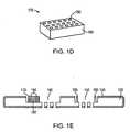
- a substrate 100is provided with one or more fill holes 110 formed in its back surface 120.
- Substrate 100preferably includes or consists essentially of a rigid and/or non-conductive material, e.g., glass or a semiconductor such as silicon.
- substrate 100includes or consists essentially of at least one unmoldable and uncurable material. At least a portion of substrate 100 forms the support structure for a high-density electronic module containing multiple microelectronic dies, as further described below.
- substrate 100is a silicon wafer with a dielectric layer disposed on at least back surface 120 and a front surface 130.
- the dielectric layermay be an oxide, e.g., silicon dioxide, and may have a thickness of approximately 1 ⁇ m.
- Fill holes 110are preferably formed in substrate 100 by forming a protective layer (not shown), e.g., photoresist, over front surface 130 and back surface 120, e.g., by a spin-on process.
- the protective layer on back surface 120is then patterned, e.g., by conventional masked photolithography, such that areas of back surface 120 where fill holes 110 are to be fabricated are substantially free of the protective layer.
- Fill holes 110are subsequently formed by, e.g., plasma or wet etching.
- fill holes 110do not completely penetrate to unetched front surface 130 of substrate 100, and have a depth in the range of approximately 200 ⁇ m to approximately 400 ⁇ m.
- the remaining thickness t 1 between the bottoms of fill holes 110 and front surface 130may be approximately 150 ⁇ m.
- each fill hole 110has a diameter of approximately 1 mm.
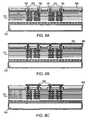
- each cavity 140is formed in front surface 130 of substrate 100.
- the depth of each cavity 140may be approximately 100 ⁇ m to approximately 250 ⁇ m, and is preferably sufficient to 1) fluidically connect cavity 140 with fill holes 110 and 2) substantially contain a microelectronic die 200 (as further described below).
- Each cavity 140is preferably in fluidic communication with multiple fill holes 110 (e.g., between approximately 25 and 36, or even up to approximately 100), but may also be in fluidic communication with as few as ten, five, or even one fill hole 110.
- Cavity 140may be formed by, e.g., conventional masked photolithography and etching.
- each post 150may be formed, the height of which is substantially equal to the depth of cavity 140.
- Each post 150may be formed during formation of cavity 140, e.g., simultaneously via the same etch process.
- Each post 150may be roughly cylindrical in shape and have a diameter of approximately 10 ⁇ m to approximately 35 ⁇ m.
- each postis non-pyramidal, i.e., has approximately the same diameter throughout its thickness, and/or is in the shape of a prism with a roughly square or rectangular cross-section.
- the postsmay have a pitch ranging from approximately 20 ⁇ m to approximately 100 ⁇ m, e.g., approximately 50 ⁇ m.
- each post 150remains rigidly connected (at one end) and includes or consists essentially of the same material as substrate 100 and/or a non-metallic material.
- each post 150includes or consists essentially of a semiconductor material such as silicon.
- each post 150includes or consists essentially of a metal such as copper.
- a layer of conductive material 160may be formed over front side 130 of substrate 100, preferably coating at least all lateral sides of each post 150 and the internal surfaces of each cavity 140.
- Conductive material 160may include or consist essentially of a metal such as copper, and may have a thickness between approximately 0.5 ⁇ m and approximately 7 ⁇ m, or even greater than approximately 7 ⁇ m.
- the thickness of conductive material 160is approximately 3 ⁇ m.
- a portion of conductive material 160(which may be a "seed portion" for electroplating) is formed by physical deposition, e.g., sputtering or evaporation, and a remaining portion is formed by electroplating.
- the physically deposited portion of conductive material 160may include or consist essentially of approximately 200 nm of copper over approximately 100 nm of titanium, and the electroplated portion may include or consist essentially of approximately 3 ⁇ m of copper.
- substantially all of conductive material 160is formed by physical deposition.
- conductive material 160may be sintered, thus reacting it with the material of post 150 to convert at least a portion of post 150 into a conductive alloy (e.g., a metal silicide).
- a conductive alloye.g., a metal silicide
- posts 150are not entirely formed of a metal.
- conductive material 160 formed within cavities 140is not removed, at least not until a suitable thinning process is performed (as described below).
- one or more posts 150are formed within cavities 140 substantially below where a microelectronic die will be positioned (as described below).
- Such posts 150may be utilized to conduct heat away from the microelectronic die to the ambient or to, e.g., a heat sink or other thermal management structure such as a heat pipe or a microfluidic layer (in a similar manner to thermal interposer 1300 described below).
- the postsmay be formed in a regular pattern below the microelectronic die, in which case the amount of heat conducted will depend on the diameter of each post, the density of the pattern, and the material of the posts.
- the postsmay be located opportunistically where "real estate" is available.
- one or more posts 150are not formed by etching of substrate 100.
- one or more posts 150may be pre-formed in a via chip 170.
- Via chip 170may include or consist essentially of a matrix 180 within which one or more posts 150 are formed.
- Matrix 180may include or consist essentially of a dielectric material or a semiconductor material, e.g., silicon.
- Posts 150preferably extend through the entire thickness of via chip 170.
- Via chip 170may be fabricated by forming one or more holes through matrix 180, e.g., by etching.
- the one or more holesmay be at least substantially filled (or have their interior surfaces coated) by a conductive material (e.g., a metal) to form post(s) 150.
- the conductive materialmay be formed by, e.g., electroplating and/or physical vapor deposition.
- one or more posts 150may be formed in via chip 170 by a process resembling a through-silicon via (TSV) process.
- TSVthrough-silicon via
- Via chip 170may be introduced into cavity 140 and encapsulated as described below with reference to microelectronic die 200.
- the functionality of via chip 170is replicated by encapsulating one or more posts 150 without a microelectronic die 200 being present.
- Figure 2depicts an exemplary apparatus for the mounting and aligning of microelectronic dies to the substrate 100, e.g., within the cavities 140 of the substrate 100.
- a plurality of microelectronic dies 200are disposed over a film 210, although, more generally, as few as a single microelectronic die 200 may be disposed over the film 210.
- one microelectronic die 200is disposed over film 210 for each cavity 140 prepared in substrate 100 as described above.
- Each microelectronic die 200may include or consist essentially of at least one semiconductor material such as Si, GaAs, or InP, and may be a bare die or a packaged die.
- At least one microelectronic die 200is a packaged assembly of multiple devices, e.g., a hermetically packaged sensor and/or microelectromechanical systems (MEMS) device.
- each microelectronic die 200is a microcontroller, a central processing unit, or other type of chip utilized in various electronic components such as sensors or computers.
- Microelectronic dies 200may have non-uniform thicknesses, and may differ in size and shape - because the microelectronic dies 200 may be encapsulated in cavities 140 as described below, individually tailored recesses or plinths may not be required for cavities 140 to be suitable to contain a wide range of different microelectronic dies 200.
- a dielectric layer 220is disposed between and in contact with each microelectronic die 200 and film 210.
- Dielectric layer 220may have a thickness of approximately 10 ⁇ m, and may be formed on film 210 by a spin-on process.
- dielectric layer 220includes or consists essentially of an unfilled polymer, e.g., a negative-toned spin-on material such as one of the various Intervia Photodielectrics (available from Rohm and Haas Company of Philadelphia, PA) or the SINR 3100 series (available from Shin-Etsu MicroSi, Inc. of Phoenix, AZ).
- a first surface of each microelectronic die 200which typically contains circuitry fabricated thereon, is in contact with film 210 or dielectric layer 220.
- dielectric layer 220is a good electrical insulator, forms uniform coatings over uneven surfaces, and is relatively transparent.
- Dielectric layer 220may be initially formed on film 210 as a liquid.
- dielectric layer 220is capable of being used to produce coatings or films with uniform thickness using equipment typically employed in fabrication of semiconductor devices. Initial heat treatments of dielectric layer 220 may allow it to become "tacky,” or at least mildly adhesive. Further heat treatments may ultimately cure/crosslink dielectric layer 220 such that it becomes a rigid structural material.
- dielectric layer 220is selected for its sensitivity to light (i.e., it is photosensitive or photoimageable). Thus, areas of dielectric layer 220 may be removed by standard photolithographic methods, e.g., prior to being fully cured. In another embodiment, dielectric layer 220 is not sensitive to light. In such a case, dielectric layer 220 may be patterned using mechanical methods such as masking, machining, deep reactive ion etching (DRIE), or ablation with a laser, before or after it is fully cured.
- DRIEdeep reactive ion etching
- film 210may be placed over die placement mask 230 containing features corresponding to the pattern of cavities 140 and posts 150 defined on substrate 100.
- Film 210 and dielectric layer 220are preferably at least partially transparent, and, as such, the microelectronic dies 200 may be placed on dielectric layer 220 in locations defined on the die placement mask 230 thereunder.
- Film 210may include or consist essentially of a substantially transparent material (e.g., Mylar or Kapton), and it (and dielectric film 220 thereover) may be supported around its perimeter by an alignment ring 240.
- alignment ring 240includes or consists essentially of a rigid material such as a metal.
- Die placement mask 230, film 210, and dielectric layer 220are preferably heated by a heated platen 250 disposed below die placement mask 240 to a temperature of approximately 60 °C to approximately 100 °C.
- the elevated temperaturesoftens dielectric layer 220 such that, as each microelectronic die 200 is placed in a desired location (dictated by the pattern on die placement mask 230), it adheres to dielectric layer 220.
- the front, active surfaces of microelectronic dies 200may be approximately coplanar, within ⁇ 2 ⁇ m.
- the front surfaces of microelectronic diesmay be substantially coated, i.e., "sealed," by dielectric layer 220.
- microelectronic dies 200 adhered to dielectric layer 220may be placed over and aligned to cavities 140 in substrate 100.
- Posts 150may be utilized as alignment marks, thus facilitating accurate alignment of microelectronic dies 200 to cavities 140.
- Substrate 100is disposed over a hotplate 300 and within a diaphragm 310. Once microelectronic dies 200 are aligned to cavities 140, alignment ring 240 is lowered such that dielectric layer 220 contacts a surface of substrate 100 and microelectronic dies 200 are substantially disposed within cavities 140.
- a substantial vacuummay be drawn in the space between film 210 and substrate 100 (now “sealed” due to the contact between diaphragms 310, 320) such that dielectric film 220 preferably (and substantially uniformly) contacts a top surface of substrate 100 and posts 150.
- dielectric film 220"seals" microelectronic dies 200 within cavities 140, as shown in Figure 4 .
- microelectronic dies 200adhere to dielectric film 220 within cavities 140, but not to an internal surface of cavities 140.
- an encapsulation chamber 400may be utilized to encapsulate the microelectronic dies 200 within cavities 140.
- Substrate 100now adhered to dielectric film 220 (which itself is disposed on film 210 and alignment ring 240) is placed within encapsulation chamber 400.
- platen 410 and pressure plate 420are disposed within encapsulation chamber 400, on opposing sides of substrate 100.
- At least one o-ring 430is disposed over platen 410, and film 440 is disposed over platen 410 and o-rings 430, thus forming pockets 445.
- Each pocket 445may contain encapsulant 450.
- Platen 410preferably includes or consists essentially of a rigid material, e.g., a metal, and is heatable.
- O-rings 430may include or consist essentially of an elastomeric material such as silicone, and film 440 may include or consist essentially of Teflon.
- Platen 410also includes holes 460 suitable for the conduction of compressed gas (e.g., compressed air), as described further below. The introduction of compressed gas through holes 460 applies pressure to the back surface of film 440 in pockets 445, and film 440 may deflect in response to the applied pressure.
- Encapsulation chamber 400also includes vacuum port 470 connected to a vacuum pump (not shown) that enables the evacuation of encapsulation chamber 400.
- microelectronic dies 200are encapsulated according to the following steps. First, platen 410 is heated to approximately 30 °C and encapsulation chamber 400 is evacuated for approximately 5 minutes in order to out-gas encapsulant 450. The vacuum in encapsulation chamber 400 also substantially prevents the formation of trapped air bubbles in cavities 140 during encapsulation of microelectronic dies 200 (as described below). Fill holes 110 are aligned above pockets 445, and force is applied to pressure plate 420 in order to seal the back surface of substrate 100 to o-rings 430 covered with film 440.
- a pressure of approximately 15 pounds per square inch (psi)is applied to the back surface of film 440 via the introduction of compressed gas through holes 460, thus forcing encapsulant 450 through fill holes 110 into cavities 140.
- Dielectric film 220supported by pressure plate 420, at least substantially prevents the flow of encapsulant 450 between microelectronic dies 200 and dielectric film 220, maintaining the substantial coplanarity of the top surfaces of microelectronic dies 200.
- the pressureis applied for approximately 5 minutes, whereupon the pressure is reduced to, e.g., approximately 1 psi.
- Platen 410is heated to approximately 60 °C for a time period sufficient to at least substantially cure encapsulant 450, e.g., approximately 4 hours.
- encapsulant 450cures, its volume may be reduced, and the pressure applied to film 440 is sufficient to inject additional encapsulant 450 into cavities 140.
- cavities 140are continuously filled with encapsulant 450 during curing, ensuring that cavities 140 are substantially or completely filled with encapsulant 450 after curing.
- Substrate 100is then removed from encapsulation chamber 400, and excess encapsulant 450 present on the back surface of substrate 100 may be removed by, e.g., scraping with a razor blade and/or application of a suitable solvent. Curing may be continued at a temperature of approximately 60 °C for a period of approximately 3 hours to approximately 5 hours. Film 210 is then removed from substrate 100, leaving dielectric layer 220 substantially or completely intact.
- the exposed surface of dielectric layer 220is preferably planar to within ⁇ 2 ⁇ m.
- the presence of dielectric layer 220 over microelectronic dies 200preferably maintains this planarity even after introduction of encapsulant 450, obviating the need to separately planarize encapsulant 450 and/or microelectronic dies 200 after encapsulation.
- other techniquesare utilized to introduce encapsulant 450 into cavities 140. For example, a syringe, an injection-molding screw, or a piston pump may be utilized to introduce encapsulant 450 into cavities 140 through fill holes 110.
- encapsulant 450includes or consists essentially of a filled polymer such as molding epoxy.
- the fillermay reduce the thermal expansion of the polymer, and may include or consist essentially of minerals, e.g., quartz, in the form of particles, e.g., spheres, having characteristic dimensions, e.g., diameters, smaller than approximately 50 ⁇ m.
- Encapsulant 450may be an insulating material having a coefficient of thermal expansion (CTE) approximately equal to the CTE of silicon.
- Encapsulant 450may be present in pockets 445 in the form of a paste or thick fluid, or in the form of a powder that melts upon application of pressure thereto. Subsequent processing may cure/crosslink encapsulant 450 such that it becomes substantially rigid.
- encapsulant 450includes or consists essentially of a heavily filled material such as Shin-Etsu Semicoat 505 or SMC-810.
- encapsulant 450 and dielectric layer 220may cooperatively encapsulate microelectronic dies 200. Encapsulation by multiple materials may be preferred, as encapsulant 450 (which is molded around the majority of each microelectronic die 200) and dielectric layer 220 (which coats the surface of each microelectronic die 200 containing active circuitry) may advantageously have different material properties and/or methods of processing. Encapsulant 450 may wet to and bond directly to dielectric layer 220, thereby forming a substantially seamless interface.
- one or more passive componentssuch as resistors, capacitors, and/or inductors may be encapsulated within substrate 100 instead of or in addition to a microelectronic die 200.
- Modules including such passive componentsmay be used as, e.g., high-density interconnect (HDI) substrates.
- the HDI substrates (and the passive components therein)may in turn be electrically connected (e.g., via contact to posts 150) to platforms such as circuit boards, and may themselves function as platforms for one or more electronic component or module (e.g., as described below).
- dielectric layer 220which is preferably photosensitive, is patterned by, e.g., conventional masked photolithography, to form via holes 500.
- dielectric layerPrior to patterning, dielectric layer may have been soft baked at approximately 90° C for approximately 60 seconds.
- Via holes 500may have a diameter between approximately 5 ⁇ m and approximately 20 ⁇ m.
- Patterned dielectric layer 220is then subjected to a hard bake of approximately 190°C for approximately 1 hour, after which it is substantially planar to within ⁇ 2 ⁇ m.
- Conductive material 510is subsequently formed over dielectric layer 220, coating and substantially or completely filling via holes 500 (thus forming conductive vias therein).
- Conductive material 510may include or consist essentially of a metal such as copper, and may have a thickness between approximately 0.5 ⁇ m and approximately 7 ⁇ m, or even greater than approximately 7 ⁇ m.
- a portion of conductive material 510(which may be a "seed portion" for electroplating) is formed by physical deposition, e.g., sputtering or evaporation, and a remaining portion is formed by electroplating.
- the electroplated portionmay be omitted, i.e., substantially all of conductive material 510 is formed by physical deposition.
- the physically deposited portion of conductive material 510may include or consist essentially of approximately 200 nm to approximately 2000 nm of copper over approximately 100 nm of titanium, and the electroplated portion may include or consist essentially of approximately 3 ⁇ m to approximately 7 ⁇ m of copper.
- Conductive material 510may also include a capping layer of approximately 100 nm of titanium that may be formed by, e.g., a physical deposition method such as sputtering.
- via holes 500are facilitated by the fact that via holes 500 only extend through the thickness of dielectric layer 220, whereupon at least some via holes 500 reach metalized posts 150.
- This arrangementobviates the need for the filling of high-aspect-ratio vias for the subsequent formation of interconnections on or near the back side of microelectronic dies 200 (after substrate thinning as described below), which may be difficult in many circumstances.
- conductive material 510is patterned by, e.g., conventional masked photolithography and etching (e.g., wet or plasma etching) to form interconnection layer 520.
- conductive material 510is etched by application of a commercially available metal etchant such as ferric chloride or chromic acid.
- interconnection layer 520preferably includes conductive lines with a minimum linewidth of less than approximately 12.5 ⁇ m, or even less than approximately 5 ⁇ m.
- solder mask 610may be formed over pre-thinned module layer 600 and patterned by, e.g., conventional masked photolithography. Solder mask 610 may include or consist essentially of a photosensitive dielectric material, e.g., those described above with reference to dielectric layer 220. Openings 620 in solder mask may be later utilized to form, e.g., solder ball connections to topmost interconnection layer 630.
- a handle wafer 700is wafer bonded to pre-thinned module layer 600 according to the following steps.
- a temporary bonding material 710is formed over pre-thinned module layer 600 by, e.g., a spin-on or silk-screen process.
- Temporary bonding material 710may include or consist essentially of, e.g., WaferBOND or WaferBOND HT-250 (both available from Brewer Science, Inc. of Rolla, MO).
- temporary bonding material 710is applied to handle wafer 700 by spinning it on at a rate of approximately 1000 to approximately 3500 rpm.
- Temporary bonding material 710may then be baked at a temperature of approximately 170 °C to approximately 220 °C for a time of approximately 7 minutes.
- Handle wafer 700may then be brought into contact with pre-thinned module layer 600 utilizing, e.g., an EVG 501 wafer bonding tool (available from EV Group E. Thallner GmbH of Austria).
- the wafer bonding processmay include applying a pressure of approximately 15 psi to handle wafer 700 and pre-thinned module layer 600, as well as applying an elevated temperature (between approximately 140 °C and approximately 220 °C) thereto.
- Handle wafer 700may include or consist essentially of glass, or may be a semiconductor (e.g., silicon) wafer having a dielectric layer (e.g., an oxide such as silicon dioxide) formed thereover.
- a dielectric layere.g., an oxide such as silicon dioxide
- a thinning processmay be performed, as illustrated in Figure 7B , on a second, opposing side of pre-thinned module layer 600.
- a thickness t 2illustrated in Figure 7A
- pre-thinned module layer 600is preferably removed, thus exposing (or even removing) at least a portion of a bottom surface of encapsulated microelectronic dies 200 and at least a portion of metalized posts 150.
- Microelectronic dies 200 and posts 150remain in their desired locations, as they are encapsulated in encapsulant 450.
- the thinning processmay include or consist essentially of mechanical grinding or lapping, e.g., on a copper lapping plate, with a polishing slurry, e.g., diamond particles suspended in a liquid such as water.
- a polishing slurrye.g., diamond particles suspended in a liquid such as water.
- an exposed surface of thinned module layer 720 thus formedis further smoothed by, e.g., chemical-mechanical polishing.
- each post 150After removal of thickness t 2 of pre-thinned module layer 600, each post 150 preferably forms at least a substantial portion of an electrical connection through substrate 100. As further described below, this connection may be utilized as an intradie interconnect (e.g., connecting the front and back sides of microelectronic die 200) and/or as an interconnect to further layers of microelectronic dies in an electronic module.
- conductive backside connections to metalized posts 150, as well as a first backside metallization layermay be formed according to the following exemplary steps.
- dielectric layer 800which is preferably photosensitive (and may include or consist essentially of materials described above for dielectric layer 220), is patterned by, e.g., conventional masked photolithography, to form backside via holes 810.
- Each backside via hole 810may have a diameter of approximately 20 ⁇ m.
- conductive material 820is subsequently formed over dielectric layer 800, substantially or completely filling backside via holes 810 (thus forming conductive vias therein).
- Conductive material 820may include or consist essentially of a metal such as copper, and may have a thickness between approximately 0.5 ⁇ m and approximately 7 ⁇ m, or even greater than approximately 7 ⁇ m.
- a portion of conductive material 820(which may be a "seed portion" for electroplating) is formed by physical deposition, e.g., sputtering or evaporation, and a remaining portion is formed by electroplating.
- the electroplated portionmay be omitted, i.e., substantially all of conductive material 820 is formed by physical deposition.
- the physically deposited portion of conductive material 820may include or consist essentially of approximately 200 nm to approximately 2000 nm of copper over approximately 100 nm of titanium, and the electroplated portion may include or consist essentially of approximately 3 ⁇ m to approximately 7 ⁇ m of copper.
- Conductive material 820may also include a capping layer of approximately 100 nm of titanium that may be formed by, e.g., a physical deposition method such as sputtering. As described above with respect to via holes 500, connections through backside via holes 810 are facilitated by the presence of metalized posts 150, which obviate the need for high-aspect-ratio via filling.
- conductive material 820is patterned by, e.g., conventional masked photolithography and etching (e.g., wet or plasma etching) to form backside interconnection layer 830.
- conductive material 820is etched by application of a commercially available metal etchant such as ferric chloride or chromic acid.
- backside interconnection layer 830preferably includes conductive lines with a minimum linewidth of less than approximately 12.5 ⁇ m, or even less than approximately 5 ⁇ m.
- Thinned module layer 720 with backside interconnection layer 830may optionally be connected to a second, similarly processed, thinned module layer 850 by, e.g., bonding the backside interconnection layers of each module 720, 850 together, as shown in Figure 9A .
- the handle wafer of the second module layer 850(not shown) may be removed, and another (or multiple) module layer(s) may be connected to the exposed surface of the second module layer 850.
- each additional module layerincludes at least one microelectronic die that is encapsulated prior to attachment to thinned module layer 720.
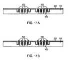
- modules 900may be individuated from the stacked module layers by, e.g., die sawing.
- Posts 150may interconnect front and back surfaces of microelectronic dies 200 or may form interdie interconnections within each module 900.
- Handle wafer 700may be removed either before or after individuation of modules 900. Removal of handle wafer 700 may be accomplished by heating to a suitable debonding temperature (which may be approximately 130 °C to approximately 250 °C, depending on the selected temporary bonding material 710), and sliding away handle wafer 700.
- Modules 900may then be suitably cleaned and utilized in any of a variety of applications, including ultra-miniature sensors, space applications with mass and size restrictions, fully integrated MEMS - complementary metal-oxide-semiconductor (MEMS-CMOS) structures, and implantable biological sensors.
- Microelectronic dies 200 within modules 900may include analog or digital integrated circuits, digital signal processors, wireless communication components such as radio frequency receivers and transmitters, optical signal processors, optical routing components such as waveguides, biological and chemical sensors, transducers, actuators, energy sources, MEMS devices, and/or passive components such as resistors, capacitors, and inductors.
- an interposer fabrication processbegins, as described above in reference to Figures 1B and 1C , with the formation of fill holes 110 and posts 150.
- a layer of conductive material 160may be formed over front side 130 of substrate 100, preferably coating at least all lateral sides of each post 150.
- the posts 150may then be encapsulated with encapsulant 450.
- Encapsulant 450preferably has a thermal expansion coefficient substantially matched to the thermal expansion coefficient of posts 150.
- a dielectric layer 220(or other suitable dielectric layer) may be formed over substrate 100 containing encapsulated posts 150 by, e.g., a spin-on process. Dielectric layer 220 is preferably patterned to form via holes 500, and conductive material 510 is formed thereover, coating and substantially or completely filling via holes 500. Conductive material 510 is then patterned and etched (as described above), forming interconnection layer 520.
- Interconnection layer 520may make electrical contact to one or more posts 150, and may be designed for subsequent connection to, e.g., an electrical component having a particular pattern or pitch of electrical contacts.
- interconnection layer 520may also make electrical contact thereto, thus facilitating the electrical connection of the passive component(s) to, e.g., a circuit board or another electrical component or module.
- multiple interconnection layers 520may be formed over substrate 100.
- an electrical interposer 1200may be formed according to the following steps. First, the opposing side of substrate 100 is thinned, thus exposing at least a bottom portion of posts 150. Posts 150 remain in their desired locations, as they are encapsulated in encapsulant 450. After thinning, the posts 150 form at least substantial portions of electrical and/or thermal connections through substrate 100. Dielectric layer is applied to the opposing side of substrate 100, and may be patterned to form via holes. A conductive material is applied and patterned to form backside interconnection layer 830.
- Backside interconnection layer 830may make electrical contact to one or more posts 150, and may be designed for subsequent connection to, e.g., an electrical component having a particular pattern or pitch of electrical contacts.
- the pattern and/or pitch of backside interconnection layermay be substantially identical or substantially different from the pattern and/or pitch of interconnection layer 520.
- electrical interposer 1200may be utilized to facilitate electrical contact between electrical components and, e.g., platforms such as circuit boards, that have different electrical contact pitches.
- electrical interposer 1200may also function as a thermal interposer (as described further below).
- a thermal interposer 1300may be formed in a manner similar to that of the above-described electrical interposer 1200, but thermal interposer 1300 may be formed without interconnection layer 520 and/or backside interconnection layer 830. Thermal interposer 1300 may be utilized to conduct heat away from one or more electrical components and/or to facilitate connection of such components to an additional heat sink.
- a backside interconnection layer 830 including or consisting essentially of a ball-grid arraymay be formed on thermal interposer 1300, and a heat sink (e.g., one including or consisting essentially of a thermally conductive material such as copper or a copper-graphite alloy) may be thermally connected to backside interconnection layer 830.
- thermal interposer 1300Heat generated from an electrical component (not pictured) in thermal contact with thermal interposer 1300 is conducted away by posts 150 and interconnection layer 520 and/or backside interconnection layer 830 (if present) either to the ambient or to a heat sink.
- a larger density of posts 150is positioned within substrate 100 in locations where such electrical components (or "hot spots” thereof) are to be attached to thermal interposer 1300.
- one or more posts positioned to make thermal contact with an electrical component (or a "hot spot” thereof)have a larger diameter (and/or a thicker layer of conductive material 160 thereon) than at least one post 150 positioned away from the component.
- thermal interposer 1300has a heat-transfer effectiveness (as defined below) of at least 2. In preferred examples, the heat-transfer effectiveness is greater than approximately 100, or even greater than approximately 1000.
- posts 150in, e.g., thermal interposer 1300
- An exemplary post 150is formed of silicon, has a uniform cylindrical cross-section with a diameter of 10 ⁇ m, and is coated with a 5 ⁇ m-thick annulus of electroplated copper.
- the total diameter of each post 150is 20 ⁇ m, and the volume fraction of each of silicon and copper per unit length is 0.5.
- the posts 150have a pitch of 50 ⁇ m, equivalent to approximately 62,500 posts/cm 2 .
- posts 150are in contact with the electrical component at one end and a heat sink at 25 °C at the other end.
- the heat flux through posts 150is modeled as steady-state heat transfer through an extended surface (a "microfin"). Such microfins are utilized to increase the heat transfer from a surface by increasing its effective surface area.
- his the heat-transfer coefficient between the microfin and stagnant air
- Pis the total perimeter of the microfins under the chip
- kis the thermal conductivity of the microfins
- a cis the total cross-sectional area of the microfins under the chip
- ⁇ baseis the temperature difference between the component and the surroundings
- ⁇ tipis the temperature difference between the heat sink and the surroundings
- Lis the x-coordinate at the tip of the microfin.
Landscapes
- Engineering & Computer Science (AREA)
- Microelectronics & Electronic Packaging (AREA)
- Power Engineering (AREA)
- Computer Hardware Design (AREA)
- Physics & Mathematics (AREA)
- Condensed Matter Physics & Semiconductors (AREA)
- General Physics & Mathematics (AREA)
- Manufacturing & Machinery (AREA)
- Ceramic Engineering (AREA)
- Internal Circuitry In Semiconductor Integrated Circuit Devices (AREA)
- Combinations Of Printed Boards (AREA)
- Structures For Mounting Electric Components On Printed Circuit Boards (AREA)
Description
- The present invention relates, in various embodiments, to the construction and fabrication of high-density heterogeneous electronic modules and electrical and/or thermal interposers.
- High-density electronic modules have been designed and fabricated to satisfy the increasing demand for high levels of functionality in small packages. Products that may be made from the modules include memory, digital logic, processing devices, and analog and RF circuits. Typically, the integration density of electronic modules is many times greater than surface mount technology ("SMT") is capable of achieving, but less than an application specific integrated circuit ("ASIC"). However, for low volume production, these modules offer an alternative to ASIC devices, as they require less set-up cost and development time. Moreover, modules may be optimized for particular applications that demand multiple functions - for example, a pre-fabricated microelectronic die optimum for each desired function is selected, and the multiple dies are then interconnected and packaged together to form the module. Often, the pre-fabricated dies will have different form factors and thicknesses, making attempts to package them together in a single module problematic. Additional difficulties may arise when attempting to vertically interconnect different layers of dies together in a single module, as the requisite processing may damage the dies in each layer.
- The fabrication of electronic modules typically features pre-thinned microelectronic dies simply positioned on an adhesive-coated substrate. A custom-machined spacer is then placed over and between the dies in order to provide a planar surface for further processing, including metal deposition, patterning, and interconnection. A thin dielectric layer is often laminated (via application of high pressure) over the dies and spacer to provide the requisite isolation between the dies and the metal interconnects. Vias to the die pads (i.e., the conductive contact pads connecting to the inner circuitry of the die) are then laser drilled and filled with a conductive material. Although high integration density may be achieved using this method, there are certain limitations. For example, dies thinned to less than 100 µm, e.g., approximately 35µm or less, might not survive the high pressure used for lamination. Furthermore, the dies that are used typically cannot be thinned after they are placed on the module substrate, limiting the module thicknesses that may be achieved. Another limitation of this method is the use of laser-drilled vias, which are typically limited in diameter to approximately 40µm. This puts constraints on die pad sizes, which restricts design choices to certain devices. In addition, spacing between dies must typically be greater than the via diameter to allow deep via formation. Finally, deep, high-aspect-ratio vias are often difficult to reliably and repeatably fill with the conductive material (as is required to interconnect multiple layers in a module).
- Moreover, it is frequently difficult to make efficient electrical contact between high- density electronic modules or other electronic components and additional modules or circuit boards. For example, a module may have electrical contacts that do not line up, or have a different pitch than, contacts on a circuit board. Time-consuming and expensive custom fabrication processes may be required in order to fabricate connectable parts. Further, it may be impossible to directly connect conventional thermal management solutions, such as heat sinks, to high-density electronic modules or other electronic components.
- Thus, in order to service the demand for increasingly small microelectronic systems, improved systems and methods for constructing high-density electronic modules and thermal and/or electrical interposers are needed.
US 5,766,986 describes a method and structure having a substrate with a fill hole formed in a first side of the substrate and a cavity formed in a second side of the substrate. An electronic device is positioned in the cavity, which open on the second side of the substrate.US 2007/0254411 discloses a printed wiring board with an array of electrical contacts and a heat sink. A passage is provided so that during a transfer moulding process, encapsulating fluid moulding compound passes latitudinally under the heat sink into a cavity.EP 1,030,369 A describes a production process for a multi-chip module structure. Bare chip devices are mounted on a base substrate, which is provided with recesses. Insulating resin is applied to fill the recesses and cover projections of the bare chip devices, and second and third insulating films are provided thereover.US-A-5008213 is also a relevant publication.- According to a first aspect of the present invention there is provided a method for constructing an electronic module as defined in claim 1.
- In accordance with certain embodiments, a technique is provided for forming high- density electronic modules that include encapsulated dies and reliable interlayer and/or intradie interconnections. The dies are preferably encapsulated with a bipartite structure that includes a dielectric layer protecting the active device surface and an encapsulant surrounding the rest of the device. Moreover, posts are preferably simultaneously formed with cavities that contain the die. These posts form at least a portion of electrical connections between dies or across a single die. In accordance with additional embodiments of the invention, modules including only the encapsulated posts (i.e., without the electronic dies) are fabricated. Such modules may be bonded to other electronic components and utilized as thermal and/or electrical interposer layers, the posts conducting electricity and/or heat through the module.
- In one aspect, embodiments of the invention feature a method for constructing an electronic module. The method includes forming at least one fill hole in a first side of a substrate and a cavity in a second side of the substrate. The cavity is in fluidic communication with the fill hole, and a die is positioned within the cavity. An encapsulant is injected through the fill hole into the cavity to encapsulate the die. The die may be disposed on a dielectric layer that is disposed over the second side of the substrate such that the die is within the cavity.
- Embodiments of the invention may include one or more of the following. At least one post may be formed within the cavity, and the post may be formed during cavity formation. Forming the post may include positioning a via chip within the cavity, and the via chip may include a matrix disposed around the post. The matrix may include silicon and the post may include a metal, e.g., copper. Forming the via chip may include defining a hole through the thickness of the matrix and forming a metal within the hole to form the post.
- A conductive material may be formed over the post and the interior surface of the cavity. The encapsulated die may be electrically connected to a second die, and at least a portion of the electrical connection may include the post. At least one layer of conductive interconnections may be formed over the second side of the substrate. At least a portion of the first side of the substrate may be removed to expose at least a portion of the die, and at least one layer of conductive interconnects may be formed over the exposed portion of the die. A handle wafer may be disposed over the second side of the substrate prior to removing at least a portion of the first side of the substrate. A temporary bonding material may be formed over the handle wafer prior to disposing it over the second side of the substrate. The encapsulated die may be individuated.
- These and other objects, along with advantages and features of the invention, will become more apparent through reference to the following description, the accompanying drawings, and the claims. Furthermore, it is to be understood that the features of the various embodiments described herein are not mutually exclusive and can exist in various combinations and permutations.
- In the drawings, like reference characters generally refer to the same parts throughout the different views. Also, the drawings are not necessarily to scale, emphasis instead generally being placed upon illustrating the principles of the invention. In the following description, various embodiments of the present invention are described with reference to the following drawings, in which:
Figs. 1A - 1C are cross-sectional views of an exemplary embodiment of a processed substrate utilized to fabricate electronic modules;Fig. 1D is a perspective view of an exemplary embodiment of a via chip containing interconnection posts;Fig. 1E is a cross-sectional view of an exemplary embodiment of a processed substrate including the via chip ofFig. 1D ;Fig. 2 is a cross-sectional view of an exemplary apparatus for the mounting and aligning of microelectronic dies;Fig. 3 is a cross-sectional view of microelectronic dies being introduced into the substrate ofFig. 1C in accordance with one embodiment of the invention;Fig. 4 is a cross-sectional view of an encapsulation apparatus utilized to encapsulate microelectronic dies in accordance with embodiments of the invention;Figs. 5A - 5C are cross-sectional views of the formation of contacts to encapsulated microelectronic dies in accordance with one embodiment of the invention;Figs. 6A and 6B are cross-sectional views of full-thickness substrate layers of an electronic module with multiple layers of interconnects in accordance with one embodiment of the invention;Fig. 7A is a cross-sectional view of a full-thickness substrate module layer attached to a handle wafer in accordance with one embodiment of the invention;Fig. 7B is a cross-sectional view of the module layer ofFig. 7A after a thinning process;Figs. 8A - 8C are cross-sectional views of the fabrication of back side contacts and interconnects on a thinned microelectronic module layer in accordance with one embodiment of the invention;Fig. 9A is a cross-sectional view of multiple thinned module layers connected together in accordance with one embodiment of the invention;Fig. 9B is a cross-sectional view of individuated microelectronic modules fabricated in accordance with embodiments of the invention;Figs. 10A and 10B are cross-sectional views of an example of a processed substrate utilized to fabricate interposer layers;Figs. 11A and 11B are cross-sectional views of the formation of contacts on an interposer including encapsulated posts;Fig. 12 is a cross-sectional view of an electrical interposer; andFig. 13 is a cross-sectional view of a thermal interposer.- Referring to
Figure 1A , asubstrate 100 is provided with one or more fill holes 110 formed in itsback surface 120.Substrate 100 preferably includes or consists essentially of a rigid and/or non-conductive material, e.g., glass or a semiconductor such as silicon. In an embodiment,substrate 100 includes or consists essentially of at least one unmoldable and uncurable material. At least a portion ofsubstrate 100 forms the support structure for a high-density electronic module containing multiple microelectronic dies, as further described below. In an embodiment,substrate 100 is a silicon wafer with a dielectric layer disposed on at least backsurface 120 and afront surface 130. The dielectric layer may be an oxide, e.g., silicon dioxide, and may have a thickness of approximately 1 µm. Fill holes 110 are preferably formed insubstrate 100 by forming a protective layer (not shown), e.g., photoresist, overfront surface 130 andback surface 120, e.g., by a spin-on process. The protective layer onback surface 120 is then patterned, e.g., by conventional masked photolithography, such that areas ofback surface 120 where fill holes 110 are to be fabricated are substantially free of the protective layer. Fill holes 110 are subsequently formed by, e.g., plasma or wet etching. In a preferred embodiment, fillholes 110 do not completely penetrate to unetchedfront surface 130 ofsubstrate 100, and have a depth in the range of approximately 200 µm to approximately 400 µm. The remaining thickness t1 between the bottoms offill holes 110 andfront surface 130 may be approximately 150 µm. In an embodiment, eachfill hole 110 has a diameter of approximately 1 mm. - Referring to
Figures 1B and 1C , at least onecavity 140 is formed infront surface 130 ofsubstrate 100. The depth of eachcavity 140 may be approximately 100 µm to approximately 250 µm, and is preferably sufficient to 1) fluidically connectcavity 140 withfill holes 110 and 2) substantially contain a microelectronic die 200 (as further described below). Eachcavity 140 is preferably in fluidic communication with multiple fill holes 110 (e.g., between approximately 25 and 36, or even up to approximately 100), but may also be in fluidic communication with as few as ten, five, or even onefill hole 110.Cavity 140 may be formed by, e.g., conventional masked photolithography and etching. Within eachcavity 140, at least onepost 150 may be formed, the height of which is substantially equal to the depth ofcavity 140. Eachpost 150 may be formed during formation ofcavity 140, e.g., simultaneously via the same etch process. Eachpost 150 may be roughly cylindrical in shape and have a diameter of approximately 10 µm to approximately 35 µm. In other embodiments, each post is non-pyramidal, i.e., has approximately the same diameter throughout its thickness, and/or is in the shape of a prism with a roughly square or rectangular cross-section. In embodiments incorporating multiple posts, the posts may have a pitch ranging from approximately 20 µm to approximately 100 µm, e.g., approximately 50 µm. In a preferred embodiment, eachpost 150 remains rigidly connected (at one end) and includes or consists essentially of the same material assubstrate 100 and/or a non-metallic material. In a preferred embodiment, eachpost 150 includes or consists essentially of a semiconductor material such as silicon. In another embodiment, eachpost 150 includes or consists essentially of a metal such as copper. As illustrated inFigure 1C , a layer ofconductive material 160 may be formed overfront side 130 ofsubstrate 100, preferably coating at least all lateral sides of eachpost 150 and the internal surfaces of eachcavity 140.Conductive material 160 may include or consist essentially of a metal such as copper, and may have a thickness between approximately 0.5 µm and approximately 7 µm, or even greater than approximately 7 µm. In an embodiment, the thickness ofconductive material 160 is approximately 3 µm. In an embodiment, a portion of conductive material 160 (which may be a "seed portion" for electroplating) is formed by physical deposition, e.g., sputtering or evaporation, and a remaining portion is formed by electroplating. The physically deposited portion ofconductive material 160 may include or consist essentially of approximately 200 nm of copper over approximately 100 nm of titanium, and the electroplated portion may include or consist essentially of approximately 3 µm of copper. In another embodiment, substantially all ofconductive material 160 is formed by physical deposition. If desired,conductive material 160 may be sintered, thus reacting it with the material ofpost 150 to convert at least a portion ofpost 150 into a conductive alloy (e.g., a metal silicide). In a preferred embodiment, even after formation ofconductive material 160 to metalizeposts 150,posts 150 are not entirely formed of a metal. In various embodiments,conductive material 160 formed withincavities 140 is not removed, at least not until a suitable thinning process is performed (as described below). In an embodiment, one ormore posts 150 are formed withincavities 140 substantially below where a microelectronic die will be positioned (as described below).Such posts 150 may be utilized to conduct heat away from the microelectronic die to the ambient or to, e.g., a heat sink or other thermal management structure such as a heat pipe or a microfluidic layer (in a similar manner tothermal interposer 1300 described below). The posts may be formed in a regular pattern below the microelectronic die, in which case the amount of heat conducted will depend on the diameter of each post, the density of the pattern, and the material of the posts. Alternatively, the posts may be located opportunistically where "real estate" is available. - Referring to
Figures 1D and 1E , in various embodiments, one ormore posts 150 are not formed by etching ofsubstrate 100. In such embodiments, one ormore posts 150 may be pre-formed in a viachip 170. Viachip 170 may include or consist essentially of amatrix 180 within which one ormore posts 150 are formed.Matrix 180 may include or consist essentially of a dielectric material or a semiconductor material, e.g., silicon.Posts 150 preferably extend through the entire thickness of viachip 170. Viachip 170 may be fabricated by forming one or more holes throughmatrix 180, e.g., by etching. The one or more holes may be at least substantially filled (or have their interior surfaces coated) by a conductive material (e.g., a metal) to form post(s) 150. The conductive material may be formed by, e.g., electroplating and/or physical vapor deposition. In this manner, one ormore posts 150 may be formed in viachip 170 by a process resembling a through-silicon via (TSV) process. Viachip 170 may be introduced intocavity 140 and encapsulated as described below with reference tomicroelectronic die 200. In another embodiment (further described below), the functionality of viachip 170 is replicated by encapsulating one ormore posts 150 without amicroelectronic die 200 being present. Figure 2 depicts an exemplary apparatus for the mounting and aligning of microelectronic dies to thesubstrate 100, e.g., within thecavities 140 of thesubstrate 100. As illustrated inFigure 2 , a plurality of microelectronic dies 200 are disposed over afilm 210, although, more generally, as few as a singlemicroelectronic die 200 may be disposed over thefilm 210. In an embodiment, one microelectronic die 200 is disposed overfilm 210 for eachcavity 140 prepared insubstrate 100 as described above. Each microelectronic die 200 may include or consist essentially of at least one semiconductor material such as Si, GaAs, or InP, and may be a bare die or a packaged die. In an embodiment, at least onemicroelectronic die 200 is a packaged assembly of multiple devices, e.g., a hermetically packaged sensor and/or microelectromechanical systems (MEMS) device. In various embodiments, eachmicroelectronic die 200 is a microcontroller, a central processing unit, or other type of chip utilized in various electronic components such as sensors or computers. Microelectronic dies 200 may have non-uniform thicknesses, and may differ in size and shape - because the microelectronic dies 200 may be encapsulated incavities 140 as described below, individually tailored recesses or plinths may not be required forcavities 140 to be suitable to contain a wide range of different microelectronic dies 200. In a preferred embodiment, adielectric layer 220 is disposed between and in contact with eachmicroelectronic die 200 andfilm 210.Dielectric layer 220 may have a thickness of approximately 10 µm, and may be formed onfilm 210 by a spin-on process. In various embodiments of the invention,dielectric layer 220 includes or consists essentially of an unfilled polymer, e.g., a negative-toned spin-on material such as one of the various Intervia Photodielectrics (available from Rohm and Haas Company of Philadelphia, PA) or the SINR 3100 series (available from Shin-Etsu MicroSi, Inc. of Phoenix, AZ). A first surface of eachmicroelectronic die 200, which typically contains circuitry fabricated thereon, is in contact withfilm 210 ordielectric layer 220.- In a preferred embodiment,
dielectric layer 220 is a good electrical insulator, forms uniform coatings over uneven surfaces, and is relatively transparent.Dielectric layer 220 may be initially formed onfilm 210 as a liquid. In one embodiment,dielectric layer 220 is capable of being used to produce coatings or films with uniform thickness using equipment typically employed in fabrication of semiconductor devices. Initial heat treatments ofdielectric layer 220 may allow it to become "tacky," or at least mildly adhesive. Further heat treatments may ultimately cure/crosslink dielectric layer 220 such that it becomes a rigid structural material. - In one embodiment,
dielectric layer 220 is selected for its sensitivity to light (i.e., it is photosensitive or photoimageable). Thus, areas ofdielectric layer 220 may be removed by standard photolithographic methods, e.g., prior to being fully cured. In another embodiment,dielectric layer 220 is not sensitive to light. In such a case,dielectric layer 220 may be patterned using mechanical methods such as masking, machining, deep reactive ion etching (DRIE), or ablation with a laser, before or after it is fully cured. - In order to facilitate accurate placement of microelectronic dies 200,
film 210 may be placed overdie placement mask 230 containing features corresponding to the pattern ofcavities 140 andposts 150 defined onsubstrate 100.Film 210 anddielectric layer 220 are preferably at least partially transparent, and, as such, the microelectronic dies 200 may be placed ondielectric layer 220 in locations defined on thedie placement mask 230 thereunder.Film 210 may include or consist essentially of a substantially transparent material (e.g., Mylar or Kapton), and it (anddielectric film 220 thereover) may be supported around its perimeter by analignment ring 240. In an embodiment,alignment ring 240 includes or consists essentially of a rigid material such as a metal.Die placement mask 230,film 210, anddielectric layer 220 are preferably heated by aheated platen 250 disposed belowdie placement mask 240 to a temperature of approximately 60 °C to approximately 100 °C. The elevated temperature softensdielectric layer 220 such that, as eachmicroelectronic die 200 is placed in a desired location (dictated by the pattern on die placement mask 230), it adheres todielectric layer 220. Once in contact withdielectric layer 220, the front, active surfaces of microelectronic dies 200 may be approximately coplanar, within ±2 µm. The front surfaces of microelectronic dies may be substantially coated, i.e., "sealed," bydielectric layer 220. - Referring to
Figure 3 , microelectronic dies 200 adhered todielectric layer 220 may be placed over and aligned tocavities 140 insubstrate 100.Posts 150 may be utilized as alignment marks, thus facilitating accurate alignment of microelectronic dies 200 tocavities 140.Substrate 100 is disposed over ahotplate 300 and within adiaphragm 310. Once microelectronic dies 200 are aligned tocavities 140,alignment ring 240 is lowered such thatdielectric layer 220 contacts a surface ofsubstrate 100 and microelectronic dies 200 are substantially disposed withincavities 140. A substantial vacuum may be drawn in the space betweenfilm 210 and substrate 100 (now "sealed" due to the contact betweendiaphragms 310, 320) such thatdielectric film 220 preferably (and substantially uniformly) contacts a top surface ofsubstrate 100 and posts 150. Thus,dielectric film 220 "seals" microelectronic dies 200 withincavities 140, as shown inFigure 4 . In an embodiment, microelectronic dies 200 adhere todielectric film 220 withincavities 140, but not to an internal surface ofcavities 140. - Referring to
Figure 4 , anencapsulation chamber 400 may be utilized to encapsulate the microelectronic dies 200 withincavities 140.Substrate 100, now adhered to dielectric film 220 (which itself is disposed onfilm 210 and alignment ring 240) is placed withinencapsulation chamber 400. Additionally disposed withinencapsulation chamber 400, on opposing sides ofsubstrate 100, are platen 410 andpressure plate 420. At least one o-ring 430 is disposed overplaten 410, andfilm 440 is disposed overplaten 410 and o-rings 430, thus forming pockets 445. Eachpocket 445 may containencapsulant 450.Platen 410 preferably includes or consists essentially of a rigid material, e.g., a metal, and is heatable. O-rings 430 may include or consist essentially of an elastomeric material such as silicone, andfilm 440 may include or consist essentially of Teflon.Platen 410 also includesholes 460 suitable for the conduction of compressed gas (e.g., compressed air), as described further below. The introduction of compressed gas throughholes 460 applies pressure to the back surface offilm 440 inpockets 445, andfilm 440 may deflect in response to the applied pressure.Encapsulation chamber 400 also includesvacuum port 470 connected to a vacuum pump (not shown) that enables the evacuation ofencapsulation chamber 400. - In an exemplary embodiment, microelectronic dies 200 are encapsulated according to the following steps. First,
platen 410 is heated to approximately 30 °C andencapsulation chamber 400 is evacuated for approximately 5 minutes in order to out-gas encapsulant 450. The vacuum inencapsulation chamber 400 also substantially prevents the formation of trapped air bubbles incavities 140 during encapsulation of microelectronic dies 200 (as described below). Fill holes 110 are aligned abovepockets 445, and force is applied topressure plate 420 in order to seal the back surface ofsubstrate 100 to o-rings 430 covered withfilm 440. A pressure of approximately 15 pounds per square inch (psi) is applied to the back surface offilm 440 via the introduction of compressed gas throughholes 460, thus forcingencapsulant 450 throughfill holes 110 intocavities 140.Dielectric film 220, supported bypressure plate 420, at least substantially prevents the flow ofencapsulant 450 between microelectronic dies 200 anddielectric film 220, maintaining the substantial coplanarity of the top surfaces of microelectronic dies 200. The pressure is applied for approximately 5 minutes, whereupon the pressure is reduced to, e.g., approximately 1 psi.Platen 410 is heated to approximately 60 °C for a time period sufficient to at least substantially cureencapsulant 450, e.g., approximately 4 hours. Asencapsulant 450 cures, its volume may be reduced, and the pressure applied to film 440 is sufficient to injectadditional encapsulant 450 intocavities 140. Thus,cavities 140 are continuously filled withencapsulant 450 during curing, ensuring thatcavities 140 are substantially or completely filled withencapsulant 450 after curing.Substrate 100 is then removed fromencapsulation chamber 400, andexcess encapsulant 450 present on the back surface ofsubstrate 100 may be removed by, e.g., scraping with a razor blade and/or application of a suitable solvent. Curing may be continued at a temperature of approximately 60 °C for a period of approximately 3 hours to approximately 5 hours.Film 210 is then removed fromsubstrate 100, leavingdielectric layer 220 substantially or completely intact. After removal offilm 210, the exposed surface ofdielectric layer 220 is preferably planar to within ±2 µm. The presence ofdielectric layer 220 over microelectronic dies 200 preferably maintains this planarity even after introduction ofencapsulant 450, obviating the need to separatelyplanarize encapsulant 450 and/or microelectronic dies 200 after encapsulation. In other embodiments, other techniques are utilized to introduceencapsulant 450 intocavities 140. For example, a syringe, an injection-molding screw, or a piston pump may be utilized to introduceencapsulant 450 intocavities 140 through fill holes 110. - In an exemplary embodiment,
encapsulant 450 includes or consists essentially of a filled polymer such as molding epoxy. The filler may reduce the thermal expansion of the polymer, and may include or consist essentially of minerals, e.g., quartz, in the form of particles, e.g., spheres, having characteristic dimensions, e.g., diameters, smaller than approximately 50 µm.Encapsulant 450 may be an insulating material having a coefficient of thermal expansion (CTE) approximately equal to the CTE of silicon.Encapsulant 450 may be present inpockets 445 in the form of a paste or thick fluid, or in the form of a powder that melts upon application of pressure thereto. Subsequent processing may cure/crosslink encapsulant 450 such that it becomes substantially rigid. In various embodiments,encapsulant 450 includes or consists essentially of a heavily filled material such as Shin-Etsu Semicoat 505 or SMC-810. - As described above,
encapsulant 450 anddielectric layer 220 may cooperatively encapsulate microelectronic dies 200. Encapsulation by multiple materials may be preferred, as encapsulant 450 (which is molded around the majority of each microelectronic die 200) and dielectric layer 220 (which coats the surface of eachmicroelectronic die 200 containing active circuitry) may advantageously have different material properties and/or methods of processing.Encapsulant 450 may wet to and bond directly todielectric layer 220, thereby forming a substantially seamless interface. - In certain embodiments, one or more passive components such as resistors, capacitors, and/or inductors may be encapsulated within
substrate 100 instead of or in addition to amicroelectronic die 200. Modules including such passive components may be used as, e.g., high-density interconnect (HDI) substrates. The HDI substrates (and the passive components therein) may in turn be electrically connected (e.g., via contact to posts 150) to platforms such as circuit boards, and may themselves function as platforms for one or more electronic component or module (e.g., as described below). - Referring to
Figures 5A - 5C , conductive connections to metalizedposts 150 and to contact pads on the surface of microelectronic dies 200, as well as a first metallization layer, may be formed according to the following exemplary steps. First,dielectric layer 220, which is preferably photosensitive, is patterned by, e.g., conventional masked photolithography, to form viaholes 500. Prior to patterning, dielectric layer may have been soft baked at approximately 90° C for approximately 60 seconds. Viaholes 500 may have a diameter between approximately 5 µm and approximately 20 µm. Patterneddielectric layer 220 is then subjected to a hard bake of approximately 190°C for approximately 1 hour, after which it is substantially planar to within ±2 µm. As illustrated inFigure 5B ,conductive material 510 is subsequently formed overdielectric layer 220, coating and substantially or completely filling via holes 500 (thus forming conductive vias therein).Conductive material 510 may include or consist essentially of a metal such as copper, and may have a thickness between approximately 0.5 µm and approximately 7 µm, or even greater than approximately 7 µm. In an embodiment, a portion of conductive material 510 (which may be a "seed portion" for electroplating) is formed by physical deposition, e.g., sputtering or evaporation, and a remaining portion is formed by electroplating. In various embodiments, the electroplated portion may be omitted, i.e., substantially all ofconductive material 510 is formed by physical deposition. The physically deposited portion ofconductive material 510 may include or consist essentially of approximately 200 nm to approximately 2000 nm of copper over approximately 100 nm of titanium, and the electroplated portion may include or consist essentially of approximately 3 µm to approximately 7 µm of copper.Conductive material 510 may also include a capping layer of approximately 100 nm of titanium that may be formed by, e.g., a physical deposition method such as sputtering. The filling of viaholes 500 withconductive material 510 is facilitated by the fact that viaholes 500 only extend through the thickness ofdielectric layer 220, whereupon at least some viaholes 500 reach metalizedposts 150. This arrangement obviates the need for the filling of high-aspect-ratio vias for the subsequent formation of interconnections on or near the back side of microelectronic dies 200 (after substrate thinning as described below), which may be difficult in many circumstances. As illustrated inFIG. 5C ,conductive material 510 is patterned by, e.g., conventional masked photolithography and etching (e.g., wet or plasma etching) to forminterconnection layer 520. In a preferred embodiment,conductive material 510 is etched by application of a commercially available metal etchant such as ferric chloride or chromic acid. After etching,interconnection layer 520 preferably includes conductive lines with a minimum linewidth of less than approximately 12.5 µm, or even less than approximately 5 µm. - Referring to
Figure 6A , after formation ofinterconnection layer 520, another dielectric film (which may be substantially identical to dielectric layer 220) may be deposited thereover, and the steps described above with reference toFigures 5A - 5C may be repeated once or even multiple times. The resultingpre-thinned module layer 600 includes a desired number and arrangement of metal interconnection layers. Referring toFigure 6B , asolder mask 610 may be formed overpre-thinned module layer 600 and patterned by, e.g., conventional masked photolithography.Solder mask 610 may include or consist essentially of a photosensitive dielectric material, e.g., those described above with reference todielectric layer 220.Openings 620 in solder mask may be later utilized to form, e.g., solder ball connections totopmost interconnection layer 630. - Referring to
Figures 7A and 7B , in various embodiments of the invention, ahandle wafer 700 is wafer bonded topre-thinned module layer 600 according to the following steps. Atemporary bonding material 710 is formed overpre-thinned module layer 600 by, e.g., a spin-on or silk-screen process.Temporary bonding material 710 may include or consist essentially of, e.g., WaferBOND or WaferBOND HT-250 (both available from Brewer Science, Inc. of Rolla, MO). In an embodiment,temporary bonding material 710 is applied to handlewafer 700 by spinning it on at a rate of approximately 1000 to approximately 3500 rpm.Temporary bonding material 710 may then be baked at a temperature of approximately 170 °C to approximately 220 °C for a time of approximately 7 minutes.Handle wafer 700 may then be brought into contact withpre-thinned module layer 600 utilizing, e.g., an EVG 501 wafer bonding tool (available from EV Group E. Thallner GmbH of Austria). The wafer bonding process may include applying a pressure of approximately 15 psi to handlewafer 700 andpre-thinned module layer 600, as well as applying an elevated temperature (between approximately 140 °C and approximately 220 °C) thereto.Handle wafer 700 may include or consist essentially of glass, or may be a semiconductor (e.g., silicon) wafer having a dielectric layer (e.g., an oxide such as silicon dioxide) formed thereover. - After
handle wafer 700 is bonded to a first surface ofpre-thinned module layer 600, a thinning process may be performed, as illustrated inFigure 7B , on a second, opposing side ofpre-thinned module layer 600. During thinning, a thickness t2 (illustrated inFigure 7A ) ofpre-thinned module layer 600 is preferably removed, thus exposing (or even removing) at least a portion of a bottom surface of encapsulated microelectronic dies 200 and at least a portion of metalized posts 150. Microelectronic dies 200 andposts 150 remain in their desired locations, as they are encapsulated inencapsulant 450. The thinning process may include or consist essentially of mechanical grinding or lapping, e.g., on a copper lapping plate, with a polishing slurry, e.g., diamond particles suspended in a liquid such as water. In an embodiment, an exposed surface of thinnedmodule layer 720 thus formed is further smoothed by, e.g., chemical-mechanical polishing. After removal of thickness t2 ofpre-thinned module layer 600, eachpost 150 preferably forms at least a substantial portion of an electrical connection throughsubstrate 100. As further described below, this connection may be utilized as an intradie interconnect (e.g., connecting the front and back sides of microelectronic die 200) and/or as an interconnect to further layers of microelectronic dies in an electronic module. - Referring to
Figures 8A - 8C , conductive backside connections to metalizedposts 150, as well as a first backside metallization layer, may be formed according to the following exemplary steps. First,dielectric layer 800, which is preferably photosensitive (and may include or consist essentially of materials described above for dielectric layer 220), is patterned by, e.g., conventional masked photolithography, to form backside viaholes 810. Each backside viahole 810 may have a diameter of approximately 20 µm. As illustrated inFigure 8B ,conductive material 820 is subsequently formed overdielectric layer 800, substantially or completely filling backside via holes 810 (thus forming conductive vias therein).Conductive material 820 may include or consist essentially of a metal such as copper, and may have a thickness between approximately 0.5 µm and approximately 7 µm, or even greater than approximately 7 µm. In an embodiment, a portion of conductive material 820 (which may be a "seed portion" for electroplating) is formed by physical deposition, e.g., sputtering or evaporation, and a remaining portion is formed by electroplating. In various embodiments, the electroplated portion may be omitted, i.e., substantially all ofconductive material 820 is formed by physical deposition. The physically deposited portion ofconductive material 820 may include or consist essentially of approximately 200 nm to approximately 2000 nm of copper over approximately 100 nm of titanium, and the electroplated portion may include or consist essentially of approximately 3 µm to approximately 7 µm of copper.Conductive material 820 may also include a capping layer of approximately 100 nm of titanium that may be formed by, e.g., a physical deposition method such as sputtering. As described above with respect to viaholes 500, connections through backside viaholes 810 are facilitated by the presence of metalizedposts 150, which obviate the need for high-aspect-ratio via filling. As illustrated inFigure 8C ,conductive material 820 is patterned by, e.g., conventional masked photolithography and etching (e.g., wet or plasma etching) to formbackside interconnection layer 830. In a preferred embodiment,conductive material 820 is etched by application of a commercially available metal etchant such as ferric chloride or chromic acid. After etching,backside interconnection layer 830 preferably includes conductive lines with a minimum linewidth of less than approximately 12.5 µm, or even less than approximately 5 µm. - Thinned
module layer 720 withbackside interconnection layer 830 may optionally be connected to a second, similarly processed, thinnedmodule layer 850 by, e.g., bonding the backside interconnection layers of eachmodule Figure 9A . The handle wafer of the second module layer 850 (not shown) may be removed, and another (or multiple) module layer(s) may be connected to the exposed surface of thesecond module layer 850. In a preferred embodiment, each additional module layer includes at least one microelectronic die that is encapsulated prior to attachment to thinnedmodule layer 720. As illustrated inFigure 9B , after a desired number (which may be none) of additional module layers is connected to thinnedmodule layer 720,modules 900 may be individuated from the stacked module layers by, e.g., die sawing.Posts 150 may interconnect front and back surfaces of microelectronic dies 200 or may form interdie interconnections within eachmodule 900.Handle wafer 700 may be removed either before or after individuation ofmodules 900. Removal ofhandle wafer 700 may be accomplished by heating to a suitable debonding temperature (which may be approximately 130 °C to approximately 250 °C, depending on the selected temporary bonding material 710), and sliding awayhandle wafer 700.Modules 900 may then be suitably cleaned and utilized in any of a variety of applications, including ultra-miniature sensors, space applications with mass and size restrictions, fully integrated MEMS - complementary metal-oxide-semiconductor (MEMS-CMOS) structures, and implantable biological sensors. Microelectronic dies 200 withinmodules 900 may include analog or digital integrated circuits, digital signal processors, wireless communication components such as radio frequency receivers and transmitters, optical signal processors, optical routing components such as waveguides, biological and chemical sensors, transducers, actuators, energy sources, MEMS devices, and/or passive components such as resistors, capacitors, and inductors. - Referring to
Figures 10A and 10B , an interposer fabrication process begins, as described above in reference toFigures 1B and 1C , with the formation offill holes 110 and posts 150. As illustrated inFigure 10B , a layer ofconductive material 160 may be formed overfront side 130 ofsubstrate 100, preferably coating at least all lateral sides of eachpost 150. - Referring to
Figures 11A and 11B (and as described above with reference toFigures 4 and5A - 5C ), theposts 150 may then be encapsulated withencapsulant 450.Encapsulant 450 preferably has a thermal expansion coefficient substantially matched to the thermal expansion coefficient ofposts 150. A dielectric layer 220 (or other suitable dielectric layer) may be formed oversubstrate 100 containing encapsulatedposts 150 by, e.g., a spin-on process.Dielectric layer 220 is preferably patterned to form viaholes 500, andconductive material 510 is formed thereover, coating and substantially or completely filling viaholes 500.Conductive material 510 is then patterned and etched (as described above), forminginterconnection layer 520.Interconnection layer 520, in turn, may make electrical contact to one ormore posts 150, and may be designed for subsequent connection to, e.g., an electrical component having a particular pattern or pitch of electrical contacts. In embodiments where one or more passive components are encapsulated withinsubstrate 100,interconnection layer 520 may also make electrical contact thereto, thus facilitating the electrical connection of the passive component(s) to, e.g., a circuit board or another electrical component or module. As described above with reference toFigures 6A and 6B ,multiple interconnection layers 520 may be formed oversubstrate 100. - Referring to
Figure 12 (and with reference toFigures 7A - 9A ), anelectrical interposer 1200 may be formed according to the following steps. First, the opposing side ofsubstrate 100 is thinned, thus exposing at least a bottom portion ofposts 150.Posts 150 remain in their desired locations, as they are encapsulated inencapsulant 450. After thinning, theposts 150 form at least substantial portions of electrical and/or thermal connections throughsubstrate 100. Dielectric layer is applied to the opposing side ofsubstrate 100, and may be patterned to form via holes. A conductive material is applied and patterned to formbackside interconnection layer 830.Backside interconnection layer 830 may make electrical contact to one ormore posts 150, and may be designed for subsequent connection to, e.g., an electrical component having a particular pattern or pitch of electrical contacts. The pattern and/or pitch of backside interconnection layer may be substantially identical or substantially different from the pattern and/or pitch ofinterconnection layer 520. Thus,electrical interposer 1200 may be utilized to facilitate electrical contact between electrical components and, e.g., platforms such as circuit boards, that have different electrical contact pitches. In some embodiments,electrical interposer 1200 may also function as a thermal interposer (as described further below). - With reference to
Figure 13 , athermal interposer 1300 may be formed in a manner similar to that of the above-describedelectrical interposer 1200, butthermal interposer 1300 may be formed withoutinterconnection layer 520 and/orbackside interconnection layer 830.Thermal interposer 1300 may be utilized to conduct heat away from one or more electrical components and/or to facilitate connection of such components to an additional heat sink. For example, abackside interconnection layer 830 including or consisting essentially of a ball-grid array may be formed onthermal interposer 1300, and a heat sink (e.g., one including or consisting essentially of a thermally conductive material such as copper or a copper-graphite alloy) may be thermally connected tobackside interconnection layer 830. Heat generated from an electrical component (not pictured) in thermal contact withthermal interposer 1300 is conducted away byposts 150 andinterconnection layer 520 and/or backside interconnection layer 830 (if present) either to the ambient or to a heat sink. In an embodiment, a larger density ofposts 150 is positioned withinsubstrate 100 in locations where such electrical components (or "hot spots" thereof) are to be attached tothermal interposer 1300. In another example, one or more posts positioned to make thermal contact with an electrical component (or a "hot spot" thereof) have a larger diameter (and/or a thicker layer ofconductive material 160 thereon) than at least onepost 150 positioned away from the component. In various examples,thermal interposer 1300 has a heat-transfer effectiveness (as defined below) of at least 2. In preferred examples, the heat-transfer effectiveness is greater than approximately 100, or even greater than approximately 1000. - The effectiveness of heat transfer through posts 150 (in, e.g., thermal interposer 1300) has been modeled for the case of an electrical component having a surface area of 1 cm2 and a temperature of 100 °C. An
exemplary post 150 is formed of silicon, has a uniform cylindrical cross-section with a diameter of 10 µm, and is coated with a 5 µm-thick annulus of electroplated copper. Thus, the total diameter of eachpost 150 is 20 µm, and the volume fraction of each of silicon and copper per unit length is 0.5. Theposts 150 have a pitch of 50 µm, equivalent to approximately 62,500 posts/cm2. We assume that heat transfer to the surrounding medium is poor (equivalent to a stagnant surrounding air space), and that the thermal conductivity ofposts 150 follows the law of mixing (i.e., is proportional to the volume percent of the silicon and copper components). Theposts 150 are in contact with the electrical component at one end and a heat sink at 25 °C at the other end. - The heat flux through
posts 150 is modeled as steady-state heat transfer through an extended surface (a "microfin"). Such microfins are utilized to increase the heat transfer from a surface by increasing its effective surface area. The figure of merit utilized to evaluate fin effectiveness is εf, the ratio of the fin heat-transfer rate to the heat-transfer rate that would exist in the absence of the fin:
- For a cylindrical microfin such as
post 150, and a heat sink at a known temperature, the heat-transfer rate qf is:
where h is the heat-transfer coefficient between the microfin and stagnant air, P is the total perimeter of the microfins under the chip, k is the thermal conductivity of the microfins, Ac is the total cross-sectional area of the microfins under the chip, θbase is the temperature difference between the component and the surroundings, θtip is the temperature difference between the heat sink and the surroundings, and L is the x-coordinate at the tip of the microfin. Utilizing the assumptions listed above, the heat-transfer rate is approximately 15.4 W, and the fin effectiveness is approximately 1,026. The assumptions utilized herein are conservative; thus, fin effectiveness of thermal interposer 1300 (and posts 150) may be even larger than this value. - The terms and expressions employed herein are used as terms and expressions of description and not of limitation, and there is no intention, in the use of such terms and expressions, of excluding any equivalents of the features shown and described or portions thereof. In addition, having described certain embodiments of the invention, it will be apparent to those of ordinary skill in the art that other embodiments incorporating the concepts disclosed herein may be used without departing from the scope of the invention as claimed. Accordingly, the described embodiments are to be considered in all respects as only illustrative and not restrictive.


Claims (14)
- A method for constructing an electronic module, the method comprising:forming a fill hole (110) in a first side of a substrate (100) and a cavity (140) in a second side of the substrate, the cavity being in fluidic communication with the fill hole;positioning a die (200) within the cavity by i) disposing the die on a dielectric layer (220) and ii) disposing the dielectric layer over the second side of the substrate such that the die is disposed within the cavity and the cavity is sealed from the second side; andinjecting an encapsulant (450) through the fill hole into the cavity to encapsulate the die positioned therein.
- The method of claim 1, further comprising forming a post (150) within the cavity (140).
- The method of claim 2, further comprising forming a conductive material (160) over the post and an interior surface of the cavity.
- The method of claim 3, further comprising electrically connecting a second die to the encapsulated die.
- The method of claim 4, wherein at least a portion of the electrical connection comprises the post.
- The method of claim 2, wherein the post is formed during formation of the cavity.
- The method of claim 2, wherein forming the post (150) comprises positioning a via chip (170) within the cavity, the via chip comprising a matrix (180) disposed around the post.
- The method of claim 7, wherein the matrix comprises silicon and the post comprises a metal.
- The method of claim 7, further comprising forming the via chip (170) by defining a hole through a thickness of the matrix and forming a metal within the hole to form the post.
- The method of claim 1, further comprising forming at least one layer of conductive interconnects over the second side of the substrate.
- The method of claim 1, further comprising removing at least a portion of the first side of the substrate to expose at least a portion of the die.
- The method of claim 11, further comprising forming at least one layer of conductive interconnects over the exposed portion of the die.
- The method of claim 11, further comprising, prior to the removing, disposing a handle wafer (700) over the second side of the substrate.
- The method of claim 13, further comprising forming a layer of temporary bonding material over the handle wafer prior to disposing the handle wafer over the second side of the substrate.
Priority Applications (2)
| Application Number | Priority Date | Filing Date | Title |
|---|---|---|---|
| EP13166078.9AEP2624290A3 (en) | 2008-04-04 | 2009-04-03 | Interposers, electronic modules, and methods for forming the same |
| EP13166066.4AEP2624289A3 (en) | 2008-04-04 | 2009-04-03 | Interposers, electronic modules, and methods for forming the same |
Applications Claiming Priority (4)
| Application Number | Priority Date | Filing Date | Title |
|---|---|---|---|
| US4251208P | 2008-04-04 | 2008-04-04 | |
| US12/164,614US8017451B2 (en) | 2008-04-04 | 2008-06-30 | Electronic modules and methods for forming the same |
| US12/407,252US8273603B2 (en) | 2008-04-04 | 2009-03-19 | Interposers, electronic modules, and methods for forming the same |
| PCT/US2009/039453WO2009124246A1 (en) | 2008-04-04 | 2009-04-03 | Interposers, electronic modules, and methods for forming the same |
Related Child Applications (4)
| Application Number | Title | Priority Date | Filing Date |
|---|---|---|---|
| EP13166066.4ADivision-IntoEP2624289A3 (en) | 2008-04-04 | 2009-04-03 | Interposers, electronic modules, and methods for forming the same |
| EP13166066.4ADivisionEP2624289A3 (en) | 2008-04-04 | 2009-04-03 | Interposers, electronic modules, and methods for forming the same |
| EP13166078.9ADivisionEP2624290A3 (en) | 2008-04-04 | 2009-04-03 | Interposers, electronic modules, and methods for forming the same |
| EP13166078.9ADivision-IntoEP2624290A3 (en) | 2008-04-04 | 2009-04-03 | Interposers, electronic modules, and methods for forming the same |
Publications (2)
| Publication Number | Publication Date |
|---|---|
| EP2277197A1 EP2277197A1 (en) | 2011-01-26 |
| EP2277197B1true EP2277197B1 (en) | 2015-01-07 |
Family
ID=41132213
Family Applications (3)
| Application Number | Title | Priority Date | Filing Date |
|---|---|---|---|
| EP13166078.9AWithdrawnEP2624290A3 (en) | 2008-04-04 | 2009-04-03 | Interposers, electronic modules, and methods for forming the same |
| EP13166066.4AWithdrawnEP2624289A3 (en) | 2008-04-04 | 2009-04-03 | Interposers, electronic modules, and methods for forming the same |
| EP09727616.6ANot-in-forceEP2277197B1 (en) | 2008-04-04 | 2009-04-03 | Method for constructing an electronic module |
Family Applications Before (2)
| Application Number | Title | Priority Date | Filing Date |
|---|---|---|---|
| EP13166078.9AWithdrawnEP2624290A3 (en) | 2008-04-04 | 2009-04-03 | Interposers, electronic modules, and methods for forming the same |
| EP13166066.4AWithdrawnEP2624289A3 (en) | 2008-04-04 | 2009-04-03 | Interposers, electronic modules, and methods for forming the same |
Country Status (3)
| Country | Link |
|---|---|
| US (1) | US8273603B2 (en) |
| EP (3) | EP2624290A3 (en) |
| WO (1) | WO2009124246A1 (en) |
Families Citing this family (27)
| Publication number | Priority date | Publication date | Assignee | Title |
|---|---|---|---|---|
| US8017451B2 (en) | 2008-04-04 | 2011-09-13 | The Charles Stark Draper Laboratory, Inc. | Electronic modules and methods for forming the same |
| US8970000B2 (en)* | 2010-01-18 | 2015-03-03 | Infineon Technologies Austria Ag | Signal transmission arrangement |
| US8508028B2 (en)* | 2010-07-16 | 2013-08-13 | Yu-Lung Huang | Chip package and method for forming the same |
| JP2013540354A (en)* | 2010-09-28 | 2013-10-31 | アドバンスド インクワイアリー システムズ インコーポレイテッド | Wafer test system and related methods of use and manufacturing |
| WO2012047875A1 (en) | 2010-10-04 | 2012-04-12 | The Charles Stark Draper Laboratory, Inc. | Fluidic constructs for electronic devices |
| JP2013545287A (en)* | 2010-10-06 | 2013-12-19 | ザ・チャールズ・スターク・ドレイパ・ラボラトリー・インコーポレイテッド | Method for forming inserts, electronic modules and the like |
| TWI436466B (en)* | 2011-04-27 | 2014-05-01 | Ind Tech Res Inst | Filled through-silicon via and the fabrication method thereof |
| CN103797575B (en)* | 2011-07-13 | 2017-05-03 | 思科技术公司 | Manufacturing a semiconductor package including an embedded circuit component within a support structure of the package |
| US9129908B2 (en) | 2011-11-15 | 2015-09-08 | Cisco Technology, Inc. | Manufacturing a semiconductor package including an embedded circuit component within a support structure of the package |
| US20130242493A1 (en)* | 2012-03-13 | 2013-09-19 | Qualcomm Mems Technologies, Inc. | Low cost interposer fabricated with additive processes |
| US9224664B2 (en) | 2012-06-06 | 2015-12-29 | The Charles Stark Draper Laboratory, Inc. | Bio-implantable hermetic integrated ultra high density device |
| US9693469B2 (en) | 2013-12-19 | 2017-06-27 | The Charles Stark Draper Laboratory, Inc. | Electronic module subassemblies |
| US9693455B1 (en) | 2014-03-27 | 2017-06-27 | STATS ChipPAC Pte. Ltd. | Integrated circuit packaging system with plated copper posts and method of manufacture thereof |
| US9154173B1 (en) | 2014-04-18 | 2015-10-06 | Raytheon Company | Linear sampler |
| US9577328B2 (en) | 2014-04-18 | 2017-02-21 | Raytheon Company | Beam forming system having linear samplers |
| US9524883B2 (en) | 2014-05-13 | 2016-12-20 | Invensas Corporation | Holding of interposers and other microelectronic workpieces in position during assembly and other processing |
| US9921377B2 (en) | 2014-07-31 | 2018-03-20 | Hewlett Packard Enterprise Department LP | Interposer registration elements |
| US10321575B2 (en)* | 2015-09-01 | 2019-06-11 | Qualcomm Incorporated | Integrated circuit (IC) module comprising an integrated circuit (IC) package and an interposer with embedded passive components |
| US20170178990A1 (en)* | 2015-12-17 | 2017-06-22 | Intel Corporation | Through-mold structures |
| US9761535B1 (en) | 2016-06-27 | 2017-09-12 | Nanya Technology Corporation | Interposer, semiconductor package with the same and method for preparing a semiconductor package with the same |
| US10423877B2 (en) | 2016-08-15 | 2019-09-24 | International Business Machines Corporation | High memory bandwidth neuromorphic computing system |
| US10062634B2 (en)* | 2016-12-21 | 2018-08-28 | Micron Technology, Inc. | Semiconductor die assembly having heat spreader that extends through underlying interposer and related technology |
| KR102444290B1 (en)* | 2017-07-18 | 2022-09-16 | 삼성전자주식회사 | Interposer and integrated circuit chip bonding method, and ultrasonic probe using same |
| US11640934B2 (en)* | 2018-03-30 | 2023-05-02 | Intel Corporation | Lithographically defined vertical interconnect access (VIA) in dielectric pockets in a package substrate |
| US10410950B1 (en)* | 2018-05-11 | 2019-09-10 | Micron Technology, Inc. | Heat spreaders for use with semiconductor devices |
| CN111792618B (en)* | 2020-06-29 | 2024-01-09 | 中国人民解放军军事科学院国防科技创新研究院 | Micro thermal array based on heterogeneous driving unit and preparation method thereof |
| CN112936727B (en)* | 2020-12-01 | 2025-05-13 | 东莞市仲康电子科技有限公司 | A PCBA board soft material in-mold injection molding process |
Citations (1)
| Publication number | Priority date | Publication date | Assignee | Title |
|---|---|---|---|---|
| US5008213A (en)* | 1988-12-09 | 1991-04-16 | The United States Of America As Represented By The Secretary Of The Air Force | Hybrid wafer scale microcircuit integration |
Family Cites Families (146)
| Publication number | Priority date | Publication date | Assignee | Title |
|---|---|---|---|---|
| US3742597A (en)* | 1971-03-17 | 1973-07-03 | Hadco Printed Circuits Inc | Method for making a coated printed circuit board |
| US4266334A (en)* | 1979-07-25 | 1981-05-12 | Rca Corporation | Manufacture of thinned substrate imagers |
| JPS6139534A (en)* | 1984-07-31 | 1986-02-25 | Sumitomo Electric Ind Ltd | Substrate materials for semiconductor devices |
| US4954875A (en) | 1986-07-17 | 1990-09-04 | Laser Dynamics, Inc. | Semiconductor wafer array with electrically conductive compliant material |
| US4897708A (en) | 1986-07-17 | 1990-01-30 | Laser Dynamics, Inc. | Semiconductor wafer array |
| US4961806A (en)* | 1986-12-10 | 1990-10-09 | Sanders Associates, Inc. | Method of making a printed circuit |
| US4800419A (en)* | 1987-01-28 | 1989-01-24 | Lsi Logic Corporation | Support assembly for integrated circuits |
| US4735679A (en)* | 1987-03-30 | 1988-04-05 | International Business Machines Corporation | Method of improving silicon-on-insulator uniformity |
| US5004498A (en)* | 1988-10-13 | 1991-04-02 | Kabushiki Kaisha Toshiba | Dispersion strengthened copper alloy and a method of manufacturing the same |
| US5162260A (en) | 1989-06-01 | 1992-11-10 | Hewlett-Packard Company | Stacked solid via formation in integrated circuit systems |
| US5108825A (en) | 1989-12-21 | 1992-04-28 | General Electric Company | Epoxy/polyimide copolymer blend dielectric and layered circuits incorporating it |
| JP2536657B2 (en)* | 1990-03-28 | 1996-09-18 | 三菱電機株式会社 | Electric device and manufacturing method thereof |
| US5446620A (en) | 1990-08-01 | 1995-08-29 | Staktek Corporation | Ultra high density integrated circuit packages |
| US5298288A (en) | 1991-02-14 | 1994-03-29 | Microelectronics And Computer Technology Corporation | Coating a heat curable liquid dielectric on a substrate |
| US5250843A (en) | 1991-03-27 | 1993-10-05 | Integrated System Assemblies Corp. | Multichip integrated circuit modules |
| US5144747A (en)* | 1991-03-27 | 1992-09-08 | Integrated System Assemblies Corporation | Apparatus and method for positioning an integrated circuit chip within a multichip module |
| US5111278A (en) | 1991-03-27 | 1992-05-05 | Eichelberger Charles W | Three-dimensional multichip module systems |
| US5172213A (en)* | 1991-05-23 | 1992-12-15 | At&T Bell Laboratories | Molded circuit package having heat dissipating post |
| US5831836A (en)* | 1992-01-30 | 1998-11-03 | Lsi Logic | Power plane for semiconductor device |
| JPH0758254A (en)* | 1993-08-19 | 1995-03-03 | Fujitsu Ltd | Multi-chip module and manufacturing method thereof |
| US5373627A (en) | 1993-11-23 | 1994-12-20 | Grebe; Kurt R. | Method of forming multi-chip module with high density interconnections |
| US5480842A (en)* | 1994-04-11 | 1996-01-02 | At&T Corp. | Method for fabricating thin, strong, and flexible die for smart cards |
| KR0149798B1 (en)* | 1994-04-15 | 1998-10-01 | 모리시다 요이치 | Semiconductor device and method of manufacture and lead frame |
| US5663106A (en)* | 1994-05-19 | 1997-09-02 | Tessera, Inc. | Method of encapsulating die and chip carrier |
| US5652463A (en)* | 1995-05-26 | 1997-07-29 | Hestia Technologies, Inc. | Transfer modlded electronic package having a passage means |
| JP2701802B2 (en)* | 1995-07-17 | 1998-01-21 | 日本電気株式会社 | Printed circuit board for bare chip mounting |
| US5866952A (en) | 1995-11-30 | 1999-02-02 | Lockheed Martin Corporation | High density interconnected circuit module with a compliant layer as part of a stress-reducing molded substrate |
| US6013948A (en)* | 1995-11-27 | 2000-01-11 | Micron Technology, Inc. | Stackable chip scale semiconductor package with mating contacts on opposed surfaces |
| US6046499A (en)* | 1996-03-27 | 2000-04-04 | Kabushiki Kaisha Toshiba | Heat transfer configuration for a semiconductor device |
| US6339875B1 (en)* | 1996-04-08 | 2002-01-22 | Heat Technology, Inc. | Method for removing heat from an integrated circuit |
| US5841193A (en) | 1996-05-20 | 1998-11-24 | Epic Technologies, Inc. | Single chip modules, repairable multichip modules, and methods of fabrication thereof |
| WO1998020528A1 (en) | 1996-11-08 | 1998-05-14 | W.L. Gore & Associates, Inc. | METHOD FOR IMPROVING RELIABILITY OF THIN CIRCUIT SUBSTRATES BY INCREASING THE Tg OF THE SUBSTRATE |
| US6551857B2 (en) | 1997-04-04 | 2003-04-22 | Elm Technology Corporation | Three dimensional structure integrated circuits |
| US6414585B1 (en)* | 1997-05-13 | 2002-07-02 | Chipscale, Inc. | Integrated passive components and package with posts |
| US5790384A (en) | 1997-06-26 | 1998-08-04 | International Business Machines Corporation | Bare die multiple dies for direct attach |
| US5981312A (en)* | 1997-06-27 | 1999-11-09 | International Business Machines Corporation | Method for injection molded flip chip encapsulation |
| US6013534A (en)* | 1997-07-25 | 2000-01-11 | The United States Of America As Represented By The National Security Agency | Method of thinning integrated circuits received in die form |
| US6081997A (en)* | 1997-08-14 | 2000-07-04 | Lsi Logic Corporation | System and method for packaging an integrated circuit using encapsulant injection |
| US6495914B1 (en)* | 1997-08-19 | 2002-12-17 | Hitachi, Ltd. | Multi-chip module structure having conductive blocks to provide electrical connection between conductors on first and second sides of a conductive base substrate |
| US7253109B2 (en) | 1997-11-26 | 2007-08-07 | Applied Materials, Inc. | Method of depositing a tantalum nitride/tantalum diffusion barrier layer system |
| US6020646A (en)* | 1997-12-05 | 2000-02-01 | The Charles Stark Draper Laboratory, Inc. | Intergrated circuit die assembly |
| US6114221A (en) | 1998-03-16 | 2000-09-05 | International Business Machines Corporation | Method and apparatus for interconnecting multiple circuit chips |
| US6307751B1 (en)* | 1998-06-01 | 2001-10-23 | Wearlogic, Inc. | Flexible circuit assembly |
| US6203967B1 (en) | 1998-07-31 | 2001-03-20 | Kulicke & Soffa Holdings, Inc. | Method for controlling stress in thin film layers deposited over a high density interconnect common circuit base |
| US6440641B1 (en) | 1998-07-31 | 2002-08-27 | Kulicke & Soffa Holdings, Inc. | Deposited thin film build-up layer dimensions as a method of relieving stress in high density interconnect printed wiring board substrates |
| US6017822A (en)* | 1998-09-16 | 2000-01-25 | The United States Of America As Represented By The National Security Agency | Method of thinning semiconductor wafer of smaller diameter than thinning equipment was designed for |
| US6117704A (en)* | 1999-03-31 | 2000-09-12 | Irvine Sensors Corporation | Stackable layers containing encapsulated chips |
| EP1041624A1 (en)* | 1999-04-02 | 2000-10-04 | Interuniversitair Microelektronica Centrum Vzw | Method of transferring ultra-thin substrates and application of the method to the manufacture of a multilayer thin film device |
| JP2001068621A (en)* | 1999-06-21 | 2001-03-16 | Shinko Electric Ind Co Ltd | Semiconductor device and its manufacture |
| US6617681B1 (en)* | 1999-06-28 | 2003-09-09 | Intel Corporation | Interposer and method of making same |
| WO2001015223A1 (en)* | 1999-08-23 | 2001-03-01 | Rohm Co., Ltd. | Semiconductor device and method of manufacture thereof |
| US6500694B1 (en) | 2000-03-22 | 2002-12-31 | Ziptronix, Inc. | Three dimensional device integration method and integrated device |
| US6294477B1 (en) | 1999-12-20 | 2001-09-25 | Thin Film Module, Inc. | Low cost high density thin film processing |
| JP2001185519A (en)* | 1999-12-24 | 2001-07-06 | Hitachi Ltd | Semiconductor device and manufacturing method thereof |
| US6333252B1 (en) | 2000-01-05 | 2001-12-25 | Advanced Semiconductor Engineering, Inc. | Low-pin-count chip package and manufacturing method thereof |
| JP2001291822A (en) | 2000-02-04 | 2001-10-19 | Seiko Epson Corp | Semiconductor chip manufacturing method and semiconductor device manufacturing method, semiconductor chip, semiconductor device, connection substrate, and electronic equipment |
| GB2360146B (en) | 2000-03-06 | 2004-04-28 | Mitel Corp | Switching power supply |
| EP1143509A3 (en)* | 2000-03-08 | 2004-04-07 | Sanyo Electric Co., Ltd. | Method of manufacturing the circuit device and circuit device |
| US6383846B1 (en)* | 2000-03-20 | 2002-05-07 | Chi-Chih Shen | Method and apparatus for molding a flip chip semiconductor device |
| US6429042B1 (en)* | 2000-04-04 | 2002-08-06 | General Electric Company | Method of reducing shear stresses on IC chips and structure formed thereby |
| JP2001313350A (en) | 2000-04-28 | 2001-11-09 | Sony Corp | Chip-shaped electronic component and its manufacturing method, and pseudo-wafer used for manufacture of chip- shaped electronic component and its manufacturing method |
| US20020071293A1 (en)* | 2000-07-13 | 2002-06-13 | Eden Richard C. | Power semiconductor switching devices, power converters, integrated circuit assemblies, integrated circuitry, power current switching methods, methods of forming a power semiconductor switching device, power conversion methods, power semiconductor switching device packaging methods, and methods a of forming power transistor |
| JP4023076B2 (en)* | 2000-07-27 | 2007-12-19 | 富士通株式会社 | Front and back conductive substrate and manufacturing method thereof |
| US6614103B1 (en)* | 2000-09-01 | 2003-09-02 | General Electric Company | Plastic packaging of LED arrays |
| US6674161B1 (en) | 2000-10-03 | 2004-01-06 | Rambus Inc. | Semiconductor stacked die devices |
| US7262082B1 (en) | 2000-10-13 | 2007-08-28 | Bridge Semiconductor Corporation | Method of making a three-dimensional stacked semiconductor package with a metal pillar and a conductive interconnect in an encapsulant aperture |
| US7129113B1 (en) | 2000-10-13 | 2006-10-31 | Bridge Semiconductor Corporation | Method of making a three-dimensional stacked semiconductor package with a metal pillar in an encapsulant aperture |
| US7009297B1 (en) | 2000-10-13 | 2006-03-07 | Bridge Semiconductor Corporation | Semiconductor chip assembly with embedded metal particle |
| US7372161B2 (en)* | 2000-10-18 | 2008-05-13 | Megica Corporation | Post passivation interconnection schemes on top of the IC chips |
| US6506681B2 (en) | 2000-12-06 | 2003-01-14 | Micron Technology, Inc. | Thin flip—chip method |
| US6632704B2 (en)* | 2000-12-19 | 2003-10-14 | Intel Corporation | Molded flip chip package |
| US6518096B2 (en)* | 2001-01-08 | 2003-02-11 | Fujitsu Limited | Interconnect assembly and Z-connection method for fine pitch substrates |
| US6910268B2 (en) | 2001-03-27 | 2005-06-28 | Formfactor, Inc. | Method for fabricating an IC interconnect system including an in-street integrated circuit wafer via |
| JP2002368168A (en)* | 2001-06-13 | 2002-12-20 | Hitachi Ltd | Composite member for semiconductor device, insulated semiconductor device using the same, or non-insulated semiconductor device |
| US6967124B1 (en) | 2001-06-19 | 2005-11-22 | Amkor Technology, Inc. | Imprinted integrated circuit substrate and method for imprinting an integrated circuit substrate |
| US6451626B1 (en) | 2001-07-27 | 2002-09-17 | Charles W.C. Lin | Three-dimensional stacked semiconductor package |
| US6765287B1 (en) | 2001-07-27 | 2004-07-20 | Charles W. C. Lin | Three-dimensional stacked semiconductor package |
| US6882034B2 (en) | 2001-08-29 | 2005-04-19 | Micron Technology, Inc. | Routing element for use in multi-chip modules, multi-chip modules including the routing element, and methods |
| US6548376B2 (en)* | 2001-08-30 | 2003-04-15 | Micron Technology, Inc. | Methods of thinning microelectronic workpieces |
| JP2003124146A (en)* | 2001-10-11 | 2003-04-25 | Lintec Corp | Method and device for peeling protecting sheet |
| US6599778B2 (en) | 2001-12-19 | 2003-07-29 | International Business Machines Corporation | Chip and wafer integration process using vertical connections |
| TW517361B (en)* | 2001-12-31 | 2003-01-11 | Megic Corp | Chip package structure and its manufacture process |
| US6884717B1 (en) | 2002-01-03 | 2005-04-26 | The United States Of America As Represented By The Secretary Of The Air Force | Stiffened backside fabrication for microwave radio frequency wafers |
| DE10200399B4 (en) | 2002-01-08 | 2008-03-27 | Advanced Micro Devices, Inc., Sunnyvale | A method for producing a three-dimensionally integrated semiconductor device and a three-dimensionally integrated semiconductor device |
| US7340181B1 (en) | 2002-05-13 | 2008-03-04 | National Semiconductor Corporation | Electrical die contact structure and fabrication method |
| US6774037B2 (en) | 2002-05-17 | 2004-08-10 | Intel Corporation | Method integrating polymeric interlayer dielectric in integrated circuits |
| US6835592B2 (en) | 2002-05-24 | 2004-12-28 | Micron Technology, Inc. | Methods for molding a semiconductor die package with enhanced thermal conductivity |
| JP4318893B2 (en) | 2002-06-03 | 2009-08-26 | 新光電気工業株式会社 | Semiconductor device and manufacturing method of semiconductor device |
| US7485489B2 (en) | 2002-06-19 | 2009-02-03 | Bjoersell Sten | Electronics circuit manufacture |
| US7535100B2 (en)* | 2002-07-12 | 2009-05-19 | The United States Of America As Represented By The Secretary Of The Navy | Wafer bonding of thinned electronic materials and circuits to high performance substrates |
| US6890618B2 (en)* | 2002-09-10 | 2005-05-10 | Tyco Electronics Corporation | Method and apparatus for retaining a thermally conductive pin in a thermal spreader plate |
| TWI290365B (en) | 2002-10-15 | 2007-11-21 | United Test Ct Inc | Stacked flip-chip package |
| JP4471563B2 (en)* | 2002-10-25 | 2010-06-02 | 株式会社ルネサステクノロジ | Manufacturing method of semiconductor device |
| US6833628B2 (en)* | 2002-12-17 | 2004-12-21 | Delphi Technologies, Inc. | Mutli-chip module |
| US7064055B2 (en) | 2002-12-31 | 2006-06-20 | Massachusetts Institute Of Technology | Method of forming a multi-layer semiconductor structure having a seamless bonding interface |
| US6762074B1 (en)* | 2003-01-21 | 2004-07-13 | Micron Technology, Inc. | Method and apparatus for forming thin microelectronic dies |
| US7388294B2 (en)* | 2003-01-27 | 2008-06-17 | Micron Technology, Inc. | Semiconductor components having stacked dice |
| KR100478498B1 (en) | 2003-01-30 | 2005-03-28 | 동부아남반도체 주식회사 | Formation method of metal line in semiconductor device |
| US6962835B2 (en) | 2003-02-07 | 2005-11-08 | Ziptronix, Inc. | Method for room temperature metal direct bonding |
| WO2004079797A2 (en) | 2003-03-05 | 2004-09-16 | Achyut Dutta | High speed electronics interconnect and method of manufacture |
| US6756305B1 (en) | 2003-04-01 | 2004-06-29 | Xilinx, Inc. | Stacked dice bonded with aluminum posts |
| US7109092B2 (en) | 2003-05-19 | 2006-09-19 | Ziptronix, Inc. | Method of room temperature covalent bonding |
| JP4369684B2 (en)* | 2003-05-26 | 2009-11-25 | 大日本印刷株式会社 | Multilayer wiring board and manufacturing method thereof |
| US6936491B2 (en)* | 2003-06-04 | 2005-08-30 | Robert Bosch Gmbh | Method of fabricating microelectromechanical systems and devices having trench isolated contacts |
| WO2005017968A2 (en)* | 2003-08-14 | 2005-02-24 | Advanced Interconnect Technologies Limited | Semiconductor device package and method for manufacturing same |
| US6943423B2 (en) | 2003-10-01 | 2005-09-13 | Optopac, Inc. | Electronic package of photo-image sensors in cellular phone camera modules, and the fabrication and assembly thereof |
| US6867073B1 (en) | 2003-10-21 | 2005-03-15 | Ziptronix, Inc. | Single mask via method and device |
| US20050093170A1 (en) | 2003-10-29 | 2005-05-05 | Texas Instruments Incorporated | Integrated interconnect package |
| US6861336B1 (en)* | 2003-11-30 | 2005-03-01 | Union Semiconductor Technology Corporation | Die thinning methods |
| US7169691B2 (en) | 2004-01-29 | 2007-01-30 | Micron Technology, Inc. | Method of fabricating wafer-level packaging with sidewall passivation and related apparatus |
| US7453150B1 (en) | 2004-04-01 | 2008-11-18 | Rensselaer Polytechnic Institute | Three-dimensional face-to-face integration assembly |
| US7084494B2 (en)* | 2004-06-18 | 2006-08-01 | Texas Instruments Incorporated | Semiconductor package having integrated metal parts for thermal enhancement |
| JP4865197B2 (en)* | 2004-06-30 | 2012-02-01 | ルネサスエレクトロニクス株式会社 | Semiconductor device and manufacturing method thereof |
| US7397066B2 (en)* | 2004-08-19 | 2008-07-08 | Micron Technology, Inc. | Microelectronic imagers with curved image sensors and methods for manufacturing microelectronic imagers |
| US7425499B2 (en) | 2004-08-24 | 2008-09-16 | Micron Technology, Inc. | Methods for forming interconnects in vias and microelectronic workpieces including such interconnects |
| US7268012B2 (en)* | 2004-08-31 | 2007-09-11 | Micron Technology, Inc. | Methods for fabrication of thin semiconductor assemblies including redistribution layers and packages and assemblies formed thereby |
| US7005319B1 (en) | 2004-11-19 | 2006-02-28 | International Business Machines Corporation | Global planarization of wafer scale package with precision die thickness control |
| US7271482B2 (en) | 2004-12-30 | 2007-09-18 | Micron Technology, Inc. | Methods for forming interconnects in microelectronic workpieces and microelectronic workpieces formed using such methods |
| US7687724B2 (en)* | 2005-01-10 | 2010-03-30 | Endicott Interconnect Technologies, Inc. | Circuitized substrate with internal resistor, method of making said circuitized substrate, and electrical assembly utilizing said circuitized substrate |
| JP4551255B2 (en)* | 2005-03-31 | 2010-09-22 | ルネサスエレクトロニクス株式会社 | Semiconductor device |
| US20060270104A1 (en)* | 2005-05-03 | 2006-11-30 | Octavio Trovarelli | Method for attaching dice to a package and arrangement of dice in a package |
| US7989958B2 (en) | 2005-06-14 | 2011-08-02 | Cufer Assett Ltd. L.L.C. | Patterned contact |
| WO2007000697A2 (en)* | 2005-06-29 | 2007-01-04 | Koninklijke Philips Electronics N.V. | Method of manufacturing an assembly and assembly |
| US7786486B2 (en)* | 2005-08-02 | 2010-08-31 | Satcon Technology Corporation | Double-sided package for power module |
| US7292381B1 (en)* | 2005-09-08 | 2007-11-06 | Hrl Laboratories, Llc | Method for conforming a micro-electronic array to arbitrary shapes |
| US20070080458A1 (en)* | 2005-10-11 | 2007-04-12 | Tsuyoshi Ogawa | Hybrid module and method of manufacturing the same |
| TWI281736B (en)* | 2005-10-26 | 2007-05-21 | Delta Electronics Inc | Power module fabrication method and structure thereof |
| JP5164362B2 (en)* | 2005-11-02 | 2013-03-21 | キヤノン株式会社 | Semiconductor embedded substrate and manufacturing method thereof |
| WO2007054867A2 (en) | 2005-11-08 | 2007-05-18 | Nxp B.V. | Producing a covered through substrate via using a temporary cap layer |
| US7274105B2 (en)* | 2005-11-28 | 2007-09-25 | Delphi Technologies, Inc. | Thermal conductive electronics substrate and assembly |
| TWI278077B (en) | 2006-02-24 | 2007-04-01 | Advanced Semiconductor Eng | Die package structure |
| WO2007130471A2 (en)* | 2006-05-01 | 2007-11-15 | The Charles Stark Draper Laboratory, Inc. | Systems and methods for high density multi-component modules |
| US8063482B2 (en)* | 2006-06-30 | 2011-11-22 | Intel Corporation | Heat spreader as mechanical reinforcement for ultra-thin die |
| US7344959B1 (en) | 2006-07-25 | 2008-03-18 | International Business Machines Corporation | Metal filled through via structure for providing vertical wafer-to-wafer interconnection |
| US7545029B2 (en)* | 2006-08-18 | 2009-06-09 | Tessera, Inc. | Stack microelectronic assemblies |
| US7482289B2 (en) | 2006-08-25 | 2009-01-27 | Battelle Memorial Institute | Methods and apparatus for depositing tantalum metal films to surfaces and substrates |
| DE102006044525B3 (en)* | 2006-09-21 | 2008-01-31 | Fraunhofer-Gesellschaft zur Förderung der angewandten Forschung e.V. | Method for production of integrated circuit, involves continuous making of flexible substrate having conductive strip structure, where flexible integrated circuit is connected with conductive strip structure of flexible substrate |
| TWI325644B (en)* | 2007-01-03 | 2010-06-01 | Chipmos Technologies Inc | Chip package and manufacturing thereof |
| JP4792143B2 (en)* | 2007-02-22 | 2011-10-12 | 株式会社デンソー | Semiconductor device and manufacturing method thereof |
| US8179693B2 (en)* | 2007-03-30 | 2012-05-15 | International Business Machines Corporation | Apparatus for electrically connecting two substrates using a land grid array connector provided with a frame structure having power distribution elements |
| US20080290494A1 (en)* | 2007-05-21 | 2008-11-27 | Markus Lutz | Backside release and/or encapsulation of microelectromechanical structures and method of manufacturing same |
| TW200901409A (en)* | 2007-06-22 | 2009-01-01 | Nan Ya Printed Circuit Board Corp | Packaging substrate with embedded chip and buried heatsink |
| US7939382B2 (en)* | 2007-06-28 | 2011-05-10 | Sandisk Corporation | Method of fabricating a semiconductor package having through holes for molding back side of package |
| US7960247B2 (en)* | 2008-04-04 | 2011-06-14 | The Charles Stark Draper Laboratory, Inc. | Die thinning processes and structures |
| US8017451B2 (en)* | 2008-04-04 | 2011-09-13 | The Charles Stark Draper Laboratory, Inc. | Electronic modules and methods for forming the same |
| FR2954580B1 (en)* | 2009-12-22 | 2011-12-09 | Commissariat Energie Atomique | METHOD FOR PRODUCING A NON-PLAN MICROELECTRONIC COMPONENT |
- 2009
- 2009-03-19USUS12/407,252patent/US8273603B2/enactiveActive
- 2009-04-03WOPCT/US2009/039453patent/WO2009124246A1/enactiveApplication Filing
- 2009-04-03EPEP13166078.9Apatent/EP2624290A3/ennot_activeWithdrawn
- 2009-04-03EPEP13166066.4Apatent/EP2624289A3/ennot_activeWithdrawn
- 2009-04-03EPEP09727616.6Apatent/EP2277197B1/ennot_activeNot-in-force
Patent Citations (1)
| Publication number | Priority date | Publication date | Assignee | Title |
|---|---|---|---|---|
| US5008213A (en)* | 1988-12-09 | 1991-04-16 | The United States Of America As Represented By The Secretary Of The Air Force | Hybrid wafer scale microcircuit integration |
Also Published As
| Publication number | Publication date |
|---|---|
| EP2624290A3 (en) | 2014-04-16 |
| US20090250249A1 (en) | 2009-10-08 |
| EP2624289A2 (en) | 2013-08-07 |
| EP2624289A3 (en) | 2014-04-16 |
| US8273603B2 (en) | 2012-09-25 |
| EP2277197A1 (en) | 2011-01-26 |
| EP2624290A2 (en) | 2013-08-07 |
| WO2009124246A1 (en) | 2009-10-08 |
Similar Documents
| Publication | Publication Date | Title |
|---|---|---|
| EP2277197B1 (en) | Method for constructing an electronic module | |
| US9425069B2 (en) | Electronic modules | |
| US20120086135A1 (en) | Interposers, electronic modules, and methods for forming the same | |
| JP7265052B2 (en) | Wafer level package with improved performance | |
| EP3607579B1 (en) | Seal for microelectronic assembly | |
| CA2464078C (en) | Semiconductor device and method of manufacturing the same | |
| US6506664B1 (en) | Method of transferring ultra-thin substrates and application of the method to the manufacture of a multi-layer thin film device | |
| EP1354351B1 (en) | Direct build-up layer on an encapsulated die package | |
| TWI546915B (en) | Circuit assemblies with multiple interposer substrates, and methods of fabrication | |
| US5373627A (en) | Method of forming multi-chip module with high density interconnections | |
| KR100908759B1 (en) | Tiny electronics package with bumpless stacked interconnect layers | |
| EP0611129B1 (en) | Embedded substrate for integrated circuit modules | |
| EP1199744B1 (en) | Microcap wafer-level package | |
| CN114864507A (en) | Semiconductor device and method of manufacturing the same | |
| Feil et al. | Ultra thin ICs and MEMS elements: techniques for wafer thinning, stress-free separation, assembly and interconnection | |
| EP1041620A2 (en) | Method of transferring ultrathin substrates and application of the method to the manufacture of a multi-layer thin film device | |
| HK1055844B (en) | Direct-build-up layer on an encapsulated die package |
Legal Events
| Date | Code | Title | Description |
|---|---|---|---|
| PUAI | Public reference made under article 153(3) epc to a published international application that has entered the european phase | Free format text:ORIGINAL CODE: 0009012 | |
| 17P | Request for examination filed | Effective date:20101103 | |
| AK | Designated contracting states | Kind code of ref document:A1 Designated state(s):AT BE BG CH CY CZ DE DK EE ES FI FR GB GR HR HU IE IS IT LI LT LU LV MC MK MT NL NO PL PT RO SE SI SK TR | |
| AX | Request for extension of the european patent | Extension state:AL BA RS | |
| 17Q | First examination report despatched | Effective date:20110513 | |
| DAX | Request for extension of the european patent (deleted) | ||
| RIN1 | Information on inventor provided before grant (corrected) | Inventor name:THOMPSON, JEFFREY, C. Inventor name:LANGDO, THOMAS, A. Inventor name:RACZ, LIVIA, M. Inventor name:THE OTHER INVENTORS HAVE AGREED TO WAIVE THEIR ENT Inventor name:TEPOLT, GARY, B. | |
| RIN1 | Information on inventor provided before grant (corrected) | Inventor name:LANGDO, THOMAS, A. Inventor name:TEPOLT, GARY, B. Inventor name:THOMPSON, JEFFREY, C. Inventor name:RACZ, LIVIA, M. Inventor name:THE OTHER INVENTORS HAVE AGREED TO WAIVE THEIR ENT | |
| REG | Reference to a national code | Ref country code:DE Ref legal event code:R079 Ref document number:602009028819 Country of ref document:DE Free format text:PREVIOUS MAIN CLASS: H01L0021680000 Ipc:B81C0001000000 | |
| RIC1 | Information provided on ipc code assigned before grant | Ipc:H01L 21/48 20060101ALI20140122BHEP Ipc:H01L 23/498 20060101ALI20140122BHEP Ipc:B81C 1/00 20060101AFI20140122BHEP Ipc:H01L 25/10 20060101ALI20140122BHEP Ipc:H01L 23/13 20060101ALI20140122BHEP Ipc:H01L 21/683 20060101ALI20140122BHEP | |
| GRAP | Despatch of communication of intention to grant a patent | Free format text:ORIGINAL CODE: EPIDOSNIGR1 | |
| INTG | Intention to grant announced | Effective date:20140729 | |
| GRAS | Grant fee paid | Free format text:ORIGINAL CODE: EPIDOSNIGR3 | |
| GRAA | (expected) grant | Free format text:ORIGINAL CODE: 0009210 | |
| AK | Designated contracting states | Kind code of ref document:B1 Designated state(s):AT BE BG CH CY CZ DE DK EE ES FI FR GB GR HR HU IE IS IT LI LT LU LV MC MK MT NL NO PL PT RO SE SI SK TR | |
| REG | Reference to a national code | Ref country code:GB Ref legal event code:FG4D | |
| REG | Reference to a national code | Ref country code:CH Ref legal event code:EP | |
| REG | Reference to a national code | Ref country code:IE Ref legal event code:FG4D | |
| REG | Reference to a national code | Ref country code:AT Ref legal event code:REF Ref document number:705555 Country of ref document:AT Kind code of ref document:T Effective date:20150215 | |
| REG | Reference to a national code | Ref country code:DE Ref legal event code:R096 Ref document number:602009028819 Country of ref document:DE Effective date:20150219 | |
| REG | Reference to a national code | Ref country code:NL Ref legal event code:VDEP Effective date:20150107 | |
| REG | Reference to a national code | Ref country code:AT Ref legal event code:MK05 Ref document number:705555 Country of ref document:AT Kind code of ref document:T Effective date:20150107 | |
| REG | Reference to a national code | Ref country code:LT Ref legal event code:MG4D | |
| PG25 | Lapsed in a contracting state [announced via postgrant information from national office to epo] | Ref country code:HR Free format text:LAPSE BECAUSE OF FAILURE TO SUBMIT A TRANSLATION OF THE DESCRIPTION OR TO PAY THE FEE WITHIN THE PRESCRIBED TIME-LIMIT Effective date:20150107 Ref country code:ES Free format text:LAPSE BECAUSE OF FAILURE TO SUBMIT A TRANSLATION OF THE DESCRIPTION OR TO PAY THE FEE WITHIN THE PRESCRIBED TIME-LIMIT Effective date:20150107 Ref country code:SE Free format text:LAPSE BECAUSE OF FAILURE TO SUBMIT A TRANSLATION OF THE DESCRIPTION OR TO PAY THE FEE WITHIN THE PRESCRIBED TIME-LIMIT Effective date:20150107 Ref country code:NO Free format text:LAPSE BECAUSE OF FAILURE TO SUBMIT A TRANSLATION OF THE DESCRIPTION OR TO PAY THE FEE WITHIN THE PRESCRIBED TIME-LIMIT Effective date:20150407 Ref country code:BG Free format text:LAPSE BECAUSE OF FAILURE TO SUBMIT A TRANSLATION OF THE DESCRIPTION OR TO PAY THE FEE WITHIN THE PRESCRIBED TIME-LIMIT Effective date:20150407 Ref country code:FI Free format text:LAPSE BECAUSE OF FAILURE TO SUBMIT A TRANSLATION OF THE DESCRIPTION OR TO PAY THE FEE WITHIN THE PRESCRIBED TIME-LIMIT Effective date:20150107 Ref country code:LT Free format text:LAPSE BECAUSE OF FAILURE TO SUBMIT A TRANSLATION OF THE DESCRIPTION OR TO PAY THE FEE WITHIN THE PRESCRIBED TIME-LIMIT Effective date:20150107 | |
| PG25 | Lapsed in a contracting state [announced via postgrant information from national office to epo] | Ref country code:PL Free format text:LAPSE BECAUSE OF FAILURE TO SUBMIT A TRANSLATION OF THE DESCRIPTION OR TO PAY THE FEE WITHIN THE PRESCRIBED TIME-LIMIT Effective date:20150107 Ref country code:AT Free format text:LAPSE BECAUSE OF FAILURE TO SUBMIT A TRANSLATION OF THE DESCRIPTION OR TO PAY THE FEE WITHIN THE PRESCRIBED TIME-LIMIT Effective date:20150107 Ref country code:NL Free format text:LAPSE BECAUSE OF FAILURE TO SUBMIT A TRANSLATION OF THE DESCRIPTION OR TO PAY THE FEE WITHIN THE PRESCRIBED TIME-LIMIT Effective date:20150107 Ref country code:LV Free format text:LAPSE BECAUSE OF FAILURE TO SUBMIT A TRANSLATION OF THE DESCRIPTION OR TO PAY THE FEE WITHIN THE PRESCRIBED TIME-LIMIT Effective date:20150107 Ref country code:IS Free format text:LAPSE BECAUSE OF FAILURE TO SUBMIT A TRANSLATION OF THE DESCRIPTION OR TO PAY THE FEE WITHIN THE PRESCRIBED TIME-LIMIT Effective date:20150507 | |
| REG | Reference to a national code | Ref country code:DE Ref legal event code:R097 Ref document number:602009028819 Country of ref document:DE | |
| PG25 | Lapsed in a contracting state [announced via postgrant information from national office to epo] | Ref country code:CZ Free format text:LAPSE BECAUSE OF FAILURE TO SUBMIT A TRANSLATION OF THE DESCRIPTION OR TO PAY THE FEE WITHIN THE PRESCRIBED TIME-LIMIT Effective date:20150107 Ref country code:SK Free format text:LAPSE BECAUSE OF FAILURE TO SUBMIT A TRANSLATION OF THE DESCRIPTION OR TO PAY THE FEE WITHIN THE PRESCRIBED TIME-LIMIT Effective date:20150107 Ref country code:RO Free format text:LAPSE BECAUSE OF FAILURE TO SUBMIT A TRANSLATION OF THE DESCRIPTION OR TO PAY THE FEE WITHIN THE PRESCRIBED TIME-LIMIT Effective date:20150107 Ref country code:DK Free format text:LAPSE BECAUSE OF FAILURE TO SUBMIT A TRANSLATION OF THE DESCRIPTION OR TO PAY THE FEE WITHIN THE PRESCRIBED TIME-LIMIT Effective date:20150107 Ref country code:EE Free format text:LAPSE BECAUSE OF FAILURE TO SUBMIT A TRANSLATION OF THE DESCRIPTION OR TO PAY THE FEE WITHIN THE PRESCRIBED TIME-LIMIT Effective date:20150107 | |
| REG | Reference to a national code | Ref country code:DE Ref legal event code:R119 Ref document number:602009028819 Country of ref document:DE | |
| PLBE | No opposition filed within time limit | Free format text:ORIGINAL CODE: 0009261 | |
| STAA | Information on the status of an ep patent application or granted ep patent | Free format text:STATUS: NO OPPOSITION FILED WITHIN TIME LIMIT | |
| PG25 | Lapsed in a contracting state [announced via postgrant information from national office to epo] | Ref country code:MC Free format text:LAPSE BECAUSE OF FAILURE TO SUBMIT A TRANSLATION OF THE DESCRIPTION OR TO PAY THE FEE WITHIN THE PRESCRIBED TIME-LIMIT Effective date:20150107 Ref country code:LU Free format text:LAPSE BECAUSE OF FAILURE TO SUBMIT A TRANSLATION OF THE DESCRIPTION OR TO PAY THE FEE WITHIN THE PRESCRIBED TIME-LIMIT Effective date:20150403 | |
| REG | Reference to a national code | Ref country code:CH Ref legal event code:PL | |
| 26N | No opposition filed | Effective date:20151008 | |
| GBPC | Gb: european patent ceased through non-payment of renewal fee | Effective date:20150407 | |
| PG25 | Lapsed in a contracting state [announced via postgrant information from national office to epo] | Ref country code:IT Free format text:LAPSE BECAUSE OF FAILURE TO SUBMIT A TRANSLATION OF THE DESCRIPTION OR TO PAY THE FEE WITHIN THE PRESCRIBED TIME-LIMIT Effective date:20150107 | |
| REG | Reference to a national code | Ref country code:IE Ref legal event code:MM4A | |
| PG25 | Lapsed in a contracting state [announced via postgrant information from national office to epo] | Ref country code:LI Free format text:LAPSE BECAUSE OF NON-PAYMENT OF DUE FEES Effective date:20150430 Ref country code:CH Free format text:LAPSE BECAUSE OF NON-PAYMENT OF DUE FEES Effective date:20150430 Ref country code:DE Free format text:LAPSE BECAUSE OF NON-PAYMENT OF DUE FEES Effective date:20151103 Ref country code:GB Free format text:LAPSE BECAUSE OF NON-PAYMENT OF DUE FEES Effective date:20150407 | |
| REG | Reference to a national code | Ref country code:FR Ref legal event code:ST Effective date:20151231 | |
| PG25 | Lapsed in a contracting state [announced via postgrant information from national office to epo] | Ref country code:SI Free format text:LAPSE BECAUSE OF FAILURE TO SUBMIT A TRANSLATION OF THE DESCRIPTION OR TO PAY THE FEE WITHIN THE PRESCRIBED TIME-LIMIT Effective date:20150107 Ref country code:FR Free format text:LAPSE BECAUSE OF NON-PAYMENT OF DUE FEES Effective date:20150430 | |
| PG25 | Lapsed in a contracting state [announced via postgrant information from national office to epo] | Ref country code:IE Free format text:LAPSE BECAUSE OF NON-PAYMENT OF DUE FEES Effective date:20150403 | |
| PG25 | Lapsed in a contracting state [announced via postgrant information from national office to epo] | Ref country code:BE Free format text:LAPSE BECAUSE OF FAILURE TO SUBMIT A TRANSLATION OF THE DESCRIPTION OR TO PAY THE FEE WITHIN THE PRESCRIBED TIME-LIMIT Effective date:20150107 | |
| PG25 | Lapsed in a contracting state [announced via postgrant information from national office to epo] | Ref country code:MT Free format text:LAPSE BECAUSE OF FAILURE TO SUBMIT A TRANSLATION OF THE DESCRIPTION OR TO PAY THE FEE WITHIN THE PRESCRIBED TIME-LIMIT Effective date:20150107 | |
| PG25 | Lapsed in a contracting state [announced via postgrant information from national office to epo] | Ref country code:HU Free format text:LAPSE BECAUSE OF FAILURE TO SUBMIT A TRANSLATION OF THE DESCRIPTION OR TO PAY THE FEE WITHIN THE PRESCRIBED TIME-LIMIT; INVALID AB INITIO Effective date:20090403 | |
| PG25 | Lapsed in a contracting state [announced via postgrant information from national office to epo] | Ref country code:GR Free format text:LAPSE BECAUSE OF FAILURE TO SUBMIT A TRANSLATION OF THE DESCRIPTION OR TO PAY THE FEE WITHIN THE PRESCRIBED TIME-LIMIT Effective date:20150107 Ref country code:CY Free format text:LAPSE BECAUSE OF FAILURE TO SUBMIT A TRANSLATION OF THE DESCRIPTION OR TO PAY THE FEE WITHIN THE PRESCRIBED TIME-LIMIT Effective date:20150107 | |
| PG25 | Lapsed in a contracting state [announced via postgrant information from national office to epo] | Ref country code:PT Free format text:LAPSE BECAUSE OF FAILURE TO SUBMIT A TRANSLATION OF THE DESCRIPTION OR TO PAY THE FEE WITHIN THE PRESCRIBED TIME-LIMIT Effective date:20150507 | |
| PG25 | Lapsed in a contracting state [announced via postgrant information from national office to epo] | Ref country code:TR Free format text:LAPSE BECAUSE OF FAILURE TO SUBMIT A TRANSLATION OF THE DESCRIPTION OR TO PAY THE FEE WITHIN THE PRESCRIBED TIME-LIMIT Effective date:20150107 | |
| PG25 | Lapsed in a contracting state [announced via postgrant information from national office to epo] | Ref country code:MK Free format text:LAPSE BECAUSE OF FAILURE TO SUBMIT A TRANSLATION OF THE DESCRIPTION OR TO PAY THE FEE WITHIN THE PRESCRIBED TIME-LIMIT Effective date:20150107 |