EP2277163B1 - System and driving method for light emitting device display - Google Patents
System and driving method for light emitting device displayDownload PDFInfo
- Publication number
- EP2277163B1 EP2277163B1EP09732338.0AEP09732338AEP2277163B1EP 2277163 B1EP2277163 B1EP 2277163B1EP 09732338 AEP09732338 AEP 09732338AEP 2277163 B1EP2277163 B1EP 2277163B1
- Authority
- EP
- European Patent Office
- Prior art keywords
- transistor
- terminal
- pixel circuit
- driving
- emission control
- Prior art date
- Legal status (The legal status is an assumption and is not a legal conclusion. Google has not performed a legal analysis and makes no representation as to the accuracy of the status listed.)
- Active
Links
- 238000000034methodMethods0.000titledescription30
- 239000003990capacitorSubstances0.000claimsdescription64
- 238000005516engineering processMethods0.000claimsdescription29
- 229910021417amorphous siliconInorganic materials0.000claimsdescription14
- 229910021420polycrystalline siliconInorganic materials0.000claimsdescription12
- 229920005591polysiliconPolymers0.000claimsdescription11
- 239000004065semiconductorSubstances0.000claimsdescription11
- 239000002184metalSubstances0.000claimsdescription3
- 229910052710siliconInorganic materials0.000claimsdescription3
- 239000010703siliconSubstances0.000claimsdescription3
- 230000036962time dependentEffects0.000claimsdescription3
- 230000001419dependent effectEffects0.000claimsdescription2
- 239000010409thin filmSubstances0.000claimsdescription2
- 238000010586diagramMethods0.000description27
- 229920001621AMOLEDPolymers0.000description23
- 101100191136Arabidopsis thaliana PCMP-A2 geneProteins0.000description15
- 101100048260Saccharomyces cerevisiae (strain ATCC 204508 / S288c) UBX2 geneProteins0.000description15
- 101100422768Saccharomyces cerevisiae (strain ATCC 204508 / S288c) SUL2 geneProteins0.000description14
- 230000000694effectsEffects0.000description8
- 229910021424microcrystalline siliconInorganic materials0.000description8
- 229910021423nanocrystalline siliconInorganic materials0.000description8
- 230000008569processEffects0.000description8
- 230000000295complement effectEffects0.000description6
- 239000011159matrix materialSubstances0.000description6
- 230000000052comparative effectEffects0.000description5
- 230000004044responseEffects0.000description5
- 241001270131Agaricus moelleriSpecies0.000description4
- 238000004519manufacturing processMethods0.000description4
- 230000007246mechanismEffects0.000description4
- 230000002123temporal effectEffects0.000description4
- XUIMIQQOPSSXEZ-UHFFFAOYSA-NSiliconChemical compound[Si]XUIMIQQOPSSXEZ-UHFFFAOYSA-N0.000description2
- 230000003071parasitic effectEffects0.000description2
- 230000002093peripheral effectEffects0.000description2
- 238000004088simulationMethods0.000description2
- 230000015556catabolic processEffects0.000description1
- 230000008859changeEffects0.000description1
- 238000006243chemical reactionMethods0.000description1
- 238000006731degradation reactionMethods0.000description1
- 238000005401electroluminescenceMethods0.000description1
- 230000010354integrationEffects0.000description1
- 239000004973liquid crystal related substanceSubstances0.000description1
- 238000012986modificationMethods0.000description1
- 230000004048modificationEffects0.000description1
- 230000002035prolonged effectEffects0.000description1
- 239000000758substrateSubstances0.000description1
Images


Classifications
- H—ELECTRICITY
- H05—ELECTRIC TECHNIQUES NOT OTHERWISE PROVIDED FOR
- H05B—ELECTRIC HEATING; ELECTRIC LIGHT SOURCES NOT OTHERWISE PROVIDED FOR; CIRCUIT ARRANGEMENTS FOR ELECTRIC LIGHT SOURCES, IN GENERAL
- H05B45/00—Circuit arrangements for operating light-emitting diodes [LED]
- H05B45/60—Circuit arrangements for operating LEDs comprising organic material, e.g. for operating organic light-emitting diodes [OLED] or polymer light-emitting diodes [PLED]
- G—PHYSICS
- G09—EDUCATION; CRYPTOGRAPHY; DISPLAY; ADVERTISING; SEALS
- G09G—ARRANGEMENTS OR CIRCUITS FOR CONTROL OF INDICATING DEVICES USING STATIC MEANS TO PRESENT VARIABLE INFORMATION
- G09G3/00—Control arrangements or circuits, of interest only in connection with visual indicators other than cathode-ray tubes
- G09G3/20—Control arrangements or circuits, of interest only in connection with visual indicators other than cathode-ray tubes for presentation of an assembly of a number of characters, e.g. a page, by composing the assembly by combination of individual elements arranged in a matrix no fixed position being assigned to or needed to be assigned to the individual characters or partial characters
- G09G3/22—Control arrangements or circuits, of interest only in connection with visual indicators other than cathode-ray tubes for presentation of an assembly of a number of characters, e.g. a page, by composing the assembly by combination of individual elements arranged in a matrix no fixed position being assigned to or needed to be assigned to the individual characters or partial characters using controlled light sources
- G09G3/30—Control arrangements or circuits, of interest only in connection with visual indicators other than cathode-ray tubes for presentation of an assembly of a number of characters, e.g. a page, by composing the assembly by combination of individual elements arranged in a matrix no fixed position being assigned to or needed to be assigned to the individual characters or partial characters using controlled light sources using electroluminescent panels
- G09G3/32—Control arrangements or circuits, of interest only in connection with visual indicators other than cathode-ray tubes for presentation of an assembly of a number of characters, e.g. a page, by composing the assembly by combination of individual elements arranged in a matrix no fixed position being assigned to or needed to be assigned to the individual characters or partial characters using controlled light sources using electroluminescent panels semiconductive, e.g. using light-emitting diodes [LED]
- G09G3/3208—Control arrangements or circuits, of interest only in connection with visual indicators other than cathode-ray tubes for presentation of an assembly of a number of characters, e.g. a page, by composing the assembly by combination of individual elements arranged in a matrix no fixed position being assigned to or needed to be assigned to the individual characters or partial characters using controlled light sources using electroluminescent panels semiconductive, e.g. using light-emitting diodes [LED] organic, e.g. using organic light-emitting diodes [OLED]
- G09G3/3225—Control arrangements or circuits, of interest only in connection with visual indicators other than cathode-ray tubes for presentation of an assembly of a number of characters, e.g. a page, by composing the assembly by combination of individual elements arranged in a matrix no fixed position being assigned to or needed to be assigned to the individual characters or partial characters using controlled light sources using electroluminescent panels semiconductive, e.g. using light-emitting diodes [LED] organic, e.g. using organic light-emitting diodes [OLED] using an active matrix
- G09G3/3233—Control arrangements or circuits, of interest only in connection with visual indicators other than cathode-ray tubes for presentation of an assembly of a number of characters, e.g. a page, by composing the assembly by combination of individual elements arranged in a matrix no fixed position being assigned to or needed to be assigned to the individual characters or partial characters using controlled light sources using electroluminescent panels semiconductive, e.g. using light-emitting diodes [LED] organic, e.g. using organic light-emitting diodes [OLED] using an active matrix with pixel circuitry controlling the current through the light-emitting element
- G09G3/3241—Control arrangements or circuits, of interest only in connection with visual indicators other than cathode-ray tubes for presentation of an assembly of a number of characters, e.g. a page, by composing the assembly by combination of individual elements arranged in a matrix no fixed position being assigned to or needed to be assigned to the individual characters or partial characters using controlled light sources using electroluminescent panels semiconductive, e.g. using light-emitting diodes [LED] organic, e.g. using organic light-emitting diodes [OLED] using an active matrix with pixel circuitry controlling the current through the light-emitting element the current through the light-emitting element being set using a data current provided by the data driver, e.g. by using a two-transistor current mirror
- G—PHYSICS
- G09—EDUCATION; CRYPTOGRAPHY; DISPLAY; ADVERTISING; SEALS
- G09G—ARRANGEMENTS OR CIRCUITS FOR CONTROL OF INDICATING DEVICES USING STATIC MEANS TO PRESENT VARIABLE INFORMATION
- G09G3/00—Control arrangements or circuits, of interest only in connection with visual indicators other than cathode-ray tubes
- G09G3/20—Control arrangements or circuits, of interest only in connection with visual indicators other than cathode-ray tubes for presentation of an assembly of a number of characters, e.g. a page, by composing the assembly by combination of individual elements arranged in a matrix no fixed position being assigned to or needed to be assigned to the individual characters or partial characters
- G09G3/22—Control arrangements or circuits, of interest only in connection with visual indicators other than cathode-ray tubes for presentation of an assembly of a number of characters, e.g. a page, by composing the assembly by combination of individual elements arranged in a matrix no fixed position being assigned to or needed to be assigned to the individual characters or partial characters using controlled light sources
- G09G3/30—Control arrangements or circuits, of interest only in connection with visual indicators other than cathode-ray tubes for presentation of an assembly of a number of characters, e.g. a page, by composing the assembly by combination of individual elements arranged in a matrix no fixed position being assigned to or needed to be assigned to the individual characters or partial characters using controlled light sources using electroluminescent panels
- G09G3/32—Control arrangements or circuits, of interest only in connection with visual indicators other than cathode-ray tubes for presentation of an assembly of a number of characters, e.g. a page, by composing the assembly by combination of individual elements arranged in a matrix no fixed position being assigned to or needed to be assigned to the individual characters or partial characters using controlled light sources using electroluminescent panels semiconductive, e.g. using light-emitting diodes [LED]
- G09G3/3208—Control arrangements or circuits, of interest only in connection with visual indicators other than cathode-ray tubes for presentation of an assembly of a number of characters, e.g. a page, by composing the assembly by combination of individual elements arranged in a matrix no fixed position being assigned to or needed to be assigned to the individual characters or partial characters using controlled light sources using electroluminescent panels semiconductive, e.g. using light-emitting diodes [LED] organic, e.g. using organic light-emitting diodes [OLED]
- G09G3/3225—Control arrangements or circuits, of interest only in connection with visual indicators other than cathode-ray tubes for presentation of an assembly of a number of characters, e.g. a page, by composing the assembly by combination of individual elements arranged in a matrix no fixed position being assigned to or needed to be assigned to the individual characters or partial characters using controlled light sources using electroluminescent panels semiconductive, e.g. using light-emitting diodes [LED] organic, e.g. using organic light-emitting diodes [OLED] using an active matrix
- G09G3/3258—Control arrangements or circuits, of interest only in connection with visual indicators other than cathode-ray tubes for presentation of an assembly of a number of characters, e.g. a page, by composing the assembly by combination of individual elements arranged in a matrix no fixed position being assigned to or needed to be assigned to the individual characters or partial characters using controlled light sources using electroluminescent panels semiconductive, e.g. using light-emitting diodes [LED] organic, e.g. using organic light-emitting diodes [OLED] using an active matrix with pixel circuitry controlling the voltage across the light-emitting element
- G—PHYSICS
- G09—EDUCATION; CRYPTOGRAPHY; DISPLAY; ADVERTISING; SEALS
- G09G—ARRANGEMENTS OR CIRCUITS FOR CONTROL OF INDICATING DEVICES USING STATIC MEANS TO PRESENT VARIABLE INFORMATION
- G09G3/00—Control arrangements or circuits, of interest only in connection with visual indicators other than cathode-ray tubes
- G09G3/20—Control arrangements or circuits, of interest only in connection with visual indicators other than cathode-ray tubes for presentation of an assembly of a number of characters, e.g. a page, by composing the assembly by combination of individual elements arranged in a matrix no fixed position being assigned to or needed to be assigned to the individual characters or partial characters
- G09G3/22—Control arrangements or circuits, of interest only in connection with visual indicators other than cathode-ray tubes for presentation of an assembly of a number of characters, e.g. a page, by composing the assembly by combination of individual elements arranged in a matrix no fixed position being assigned to or needed to be assigned to the individual characters or partial characters using controlled light sources
- G09G3/30—Control arrangements or circuits, of interest only in connection with visual indicators other than cathode-ray tubes for presentation of an assembly of a number of characters, e.g. a page, by composing the assembly by combination of individual elements arranged in a matrix no fixed position being assigned to or needed to be assigned to the individual characters or partial characters using controlled light sources using electroluminescent panels
- G09G3/32—Control arrangements or circuits, of interest only in connection with visual indicators other than cathode-ray tubes for presentation of an assembly of a number of characters, e.g. a page, by composing the assembly by combination of individual elements arranged in a matrix no fixed position being assigned to or needed to be assigned to the individual characters or partial characters using controlled light sources using electroluminescent panels semiconductive, e.g. using light-emitting diodes [LED]
- G09G3/3208—Control arrangements or circuits, of interest only in connection with visual indicators other than cathode-ray tubes for presentation of an assembly of a number of characters, e.g. a page, by composing the assembly by combination of individual elements arranged in a matrix no fixed position being assigned to or needed to be assigned to the individual characters or partial characters using controlled light sources using electroluminescent panels semiconductive, e.g. using light-emitting diodes [LED] organic, e.g. using organic light-emitting diodes [OLED]
- G09G3/3275—Details of drivers for data electrodes
- G09G3/3283—Details of drivers for data electrodes in which the data driver supplies a variable data current for setting the current through, or the voltage across, the light-emitting elements
- G—PHYSICS
- G09—EDUCATION; CRYPTOGRAPHY; DISPLAY; ADVERTISING; SEALS
- G09G—ARRANGEMENTS OR CIRCUITS FOR CONTROL OF INDICATING DEVICES USING STATIC MEANS TO PRESENT VARIABLE INFORMATION
- G09G3/00—Control arrangements or circuits, of interest only in connection with visual indicators other than cathode-ray tubes
- G09G3/20—Control arrangements or circuits, of interest only in connection with visual indicators other than cathode-ray tubes for presentation of an assembly of a number of characters, e.g. a page, by composing the assembly by combination of individual elements arranged in a matrix no fixed position being assigned to or needed to be assigned to the individual characters or partial characters
- G09G3/22—Control arrangements or circuits, of interest only in connection with visual indicators other than cathode-ray tubes for presentation of an assembly of a number of characters, e.g. a page, by composing the assembly by combination of individual elements arranged in a matrix no fixed position being assigned to or needed to be assigned to the individual characters or partial characters using controlled light sources
- G09G3/30—Control arrangements or circuits, of interest only in connection with visual indicators other than cathode-ray tubes for presentation of an assembly of a number of characters, e.g. a page, by composing the assembly by combination of individual elements arranged in a matrix no fixed position being assigned to or needed to be assigned to the individual characters or partial characters using controlled light sources using electroluminescent panels
- G09G3/32—Control arrangements or circuits, of interest only in connection with visual indicators other than cathode-ray tubes for presentation of an assembly of a number of characters, e.g. a page, by composing the assembly by combination of individual elements arranged in a matrix no fixed position being assigned to or needed to be assigned to the individual characters or partial characters using controlled light sources using electroluminescent panels semiconductive, e.g. using light-emitting diodes [LED]
- G09G3/3208—Control arrangements or circuits, of interest only in connection with visual indicators other than cathode-ray tubes for presentation of an assembly of a number of characters, e.g. a page, by composing the assembly by combination of individual elements arranged in a matrix no fixed position being assigned to or needed to be assigned to the individual characters or partial characters using controlled light sources using electroluminescent panels semiconductive, e.g. using light-emitting diodes [LED] organic, e.g. using organic light-emitting diodes [OLED]
- G09G3/3275—Details of drivers for data electrodes
- G09G3/3291—Details of drivers for data electrodes in which the data driver supplies a variable data voltage for setting the current through, or the voltage across, the light-emitting elements
- H—ELECTRICITY
- H05—ELECTRIC TECHNIQUES NOT OTHERWISE PROVIDED FOR
- H05B—ELECTRIC HEATING; ELECTRIC LIGHT SOURCES NOT OTHERWISE PROVIDED FOR; CIRCUIT ARRANGEMENTS FOR ELECTRIC LIGHT SOURCES, IN GENERAL
- H05B45/00—Circuit arrangements for operating light-emitting diodes [LED]
- H05B45/40—Details of LED load circuits
- H05B45/44—Details of LED load circuits with an active control inside an LED matrix
- H05B45/48—Details of LED load circuits with an active control inside an LED matrix having LEDs organised in strings and incorporating parallel shunting devices
- G—PHYSICS
- G09—EDUCATION; CRYPTOGRAPHY; DISPLAY; ADVERTISING; SEALS
- G09G—ARRANGEMENTS OR CIRCUITS FOR CONTROL OF INDICATING DEVICES USING STATIC MEANS TO PRESENT VARIABLE INFORMATION
- G09G2300/00—Aspects of the constitution of display devices
- G09G2300/04—Structural and physical details of display devices
- G09G2300/0421—Structural details of the set of electrodes
- G09G2300/043—Compensation electrodes or other additional electrodes in matrix displays related to distortions or compensation signals, e.g. for modifying TFT threshold voltage in column driver
- G—PHYSICS
- G09—EDUCATION; CRYPTOGRAPHY; DISPLAY; ADVERTISING; SEALS
- G09G—ARRANGEMENTS OR CIRCUITS FOR CONTROL OF INDICATING DEVICES USING STATIC MEANS TO PRESENT VARIABLE INFORMATION
- G09G2300/00—Aspects of the constitution of display devices
- G09G2300/08—Active matrix structure, i.e. with use of active elements, inclusive of non-linear two terminal elements, in the pixels together with light emitting or modulating elements
- G09G2300/0809—Several active elements per pixel in active matrix panels
- G09G2300/0819—Several active elements per pixel in active matrix panels used for counteracting undesired variations, e.g. feedback or autozeroing
- G—PHYSICS
- G09—EDUCATION; CRYPTOGRAPHY; DISPLAY; ADVERTISING; SEALS
- G09G—ARRANGEMENTS OR CIRCUITS FOR CONTROL OF INDICATING DEVICES USING STATIC MEANS TO PRESENT VARIABLE INFORMATION
- G09G2300/00—Aspects of the constitution of display devices
- G09G2300/08—Active matrix structure, i.e. with use of active elements, inclusive of non-linear two terminal elements, in the pixels together with light emitting or modulating elements
- G09G2300/0809—Several active elements per pixel in active matrix panels
- G09G2300/0842—Several active elements per pixel in active matrix panels forming a memory circuit, e.g. a dynamic memory with one capacitor
- G09G2300/0852—Several active elements per pixel in active matrix panels forming a memory circuit, e.g. a dynamic memory with one capacitor being a dynamic memory with more than one capacitor
- G—PHYSICS
- G09—EDUCATION; CRYPTOGRAPHY; DISPLAY; ADVERTISING; SEALS
- G09G—ARRANGEMENTS OR CIRCUITS FOR CONTROL OF INDICATING DEVICES USING STATIC MEANS TO PRESENT VARIABLE INFORMATION
- G09G2300/00—Aspects of the constitution of display devices
- G09G2300/08—Active matrix structure, i.e. with use of active elements, inclusive of non-linear two terminal elements, in the pixels together with light emitting or modulating elements
- G09G2300/0809—Several active elements per pixel in active matrix panels
- G09G2300/0842—Several active elements per pixel in active matrix panels forming a memory circuit, e.g. a dynamic memory with one capacitor
- G09G2300/0861—Several active elements per pixel in active matrix panels forming a memory circuit, e.g. a dynamic memory with one capacitor with additional control of the display period without amending the charge stored in a pixel memory, e.g. by means of additional select electrodes
- G—PHYSICS
- G09—EDUCATION; CRYPTOGRAPHY; DISPLAY; ADVERTISING; SEALS
- G09G—ARRANGEMENTS OR CIRCUITS FOR CONTROL OF INDICATING DEVICES USING STATIC MEANS TO PRESENT VARIABLE INFORMATION
- G09G2310/00—Command of the display device
- G09G2310/02—Addressing, scanning or driving the display screen or processing steps related thereto
- G09G2310/0262—The addressing of the pixel, in a display other than an active matrix LCD, involving the control of two or more scan electrodes or two or more data electrodes, e.g. pixel voltage dependent on signals of two data electrodes
- G—PHYSICS
- G09—EDUCATION; CRYPTOGRAPHY; DISPLAY; ADVERTISING; SEALS
- G09G—ARRANGEMENTS OR CIRCUITS FOR CONTROL OF INDICATING DEVICES USING STATIC MEANS TO PRESENT VARIABLE INFORMATION
- G09G2320/00—Control of display operating conditions
- G09G2320/02—Improving the quality of display appearance
- G09G2320/0252—Improving the response speed
- G—PHYSICS
- G09—EDUCATION; CRYPTOGRAPHY; DISPLAY; ADVERTISING; SEALS
- G09G—ARRANGEMENTS OR CIRCUITS FOR CONTROL OF INDICATING DEVICES USING STATIC MEANS TO PRESENT VARIABLE INFORMATION
- G09G2320/00—Control of display operating conditions
- G09G2320/04—Maintaining the quality of display appearance
- G09G2320/043—Preventing or counteracting the effects of ageing
- G09G2320/045—Compensation of drifts in the characteristics of light emitting or modulating elements
Definitions
- the present inventionrelates to a light emitting device displays, and more specifically to a driving technique for the light emitting device displays.
- AMOLEDactive-matrix organic light-emitting diode
- a-Siamorphous silicon
- poly-siliconpoly-silicon
- organicorganic, or other driving backplane technology
- An AMOLED display using a-Si backplaneshas the advantages which include low temperature fabrication that broadens the use of different substrates and makes flexible displays feasible, and its low cost fabrication is well-established and yields high resolution displays with a wide viewing angle.
- An AMOLED displayincludes an array of rows and columns of pixels, each having an organic light-emitting diode (OLED) and backplane electronics arranged in the array of rows and columns. Since the OLED is a current driven device, the pixel circuit of the AMOLED should be capable of providing an accurate and constant drive current.
- OLEDorganic light-emitting diode
- One method that has been employed to drive the AMOLED displayis programming the AMOLED pixel directly with current.
- the small current required by the OLEDcoupled with a large parasitic capacitance, undesirably increases the settling time of the programming of the current-programmed AMOLED display.
- the transistorsmust work in sub-threshold regime to provide the small current required by the OLEDs, which is not ideal. Therefore, in order to use current-programmed AMOLED pixel circuits, suitable driving schemes are desirable.
- Current scalingis one method that can be used to manage issues associated with the small current required by the OLEDs.
- the current passing through the OLEDcan be scaled by having a smaller drive transistor as compared to the mirror transistor.
- this methodis not applicable for other current-programmed pixel circuits. Also, by resizing the two mirror transistors the effect of mismatch increases.
- Patent application publication CA 2523841 Aprovides an active matrix light emitting device display and its driving technique is provided.
- the pixelincludes a light emitting device and a plurality of transistors.
- a capacitormay be used to store a voltage applied to a driving transistor so that a current through the light emitting device is independent of any shifts of the transistor and light emitting device characteristics.
- a bias data and a programming dataare provided to the pixel circuit in accordance with a driving scheme.
- Patent application publication US 2006/145967 Arelates to an organic electro-luminescence device that includes a drive unit having first to fourth transistors and a capacitor, and an organic light emitting diode (OLED) controlled by the drive unit, wherein the first transistor has its gate, drain and source connected to a first node, a second node and a power voltage supply line, respectively; the second transistor has its drain and source connected to the OLED and the second node, respectively; the third transistor has its gate, drain and source connected to a first select signal line, the second node and the first node, respectively; the fourth transistor has its gate, drain and source connected to the first select signal line, a data line, and the second node, respectively; and the capacitor is connected to the first node and a predetermined signal line.
- OLEDorganic light emitting diode
- Patent application publication US 2006/0077194 A1describes another pixel circuit of an active matrix OLED display addressing transistor threshold voltage variations and voltage drop on the power supply lines.
- the pixel circuitcomprises a first switching transistor (M1) connecting the data line (Dm) to a first node (A) in response to a first scan line signal (S1.n), a fourth switching transistor (M5) connecting the pixel power line (Vdd) to a third node (C) in response to a third scan line signal (S3.n), a capacitor (Cst) connected between the first node (A) and the third node (C), a third switching transistor (M3) connecting the first node (A) to a second node (B) in response to a second scan line signal (S2.n), a driving transistor (M4) for supplying current from the third node (C) to an OLED according to the voltage of the second node (B) applied to its gate electrode, a second switching transistor (M2) supplying a compensation power (Vinit) to the second
- a pixel circuitwhich includes a light emitting device, a driving transistor for providing a pixel current to the light emitting device, a storage capacitor provided between a data line for providing programming voltage data and the gate terminal of the driving transistor, a first switch transistor provided between the gate terminal of the driving transistor and the light emitting device, and a second switch transistor provided between the light emitting device and a bias line for providing a bias current to the first terminal of the driving transistor during a programming cycle.
- a pixel circuitwhich includes a light emitting device, a storage capacitor, a driving transistor for providing a pixel current to the light emitting device, a plurality of first switch transistors operated by a first select line, one of the first switch transistors being provided between the storage capacitor and a data line for providing programming voltage data, a plurality of second switch transistors operated by a second select line, one of the second switch transistor being provided between the driving transistor and a bias line for providing a bias current to the first terminal of the driving transistor during a programming cycle; and an emission control circuit for setting the pixel circuit into an emission mode.
- a display systemwhich includes a pixel array having a plurality of pixel circuits, a first driver for selecting the pixel circuit, a second driver for providing the programming voltage data, and a current source for operating on the bias line.
- a method of driving a pixel circuitthe pixel circuit having a driving transistor for providing a pixel current to a light emitting device, a storage capacitor coupled to a data line, and a switch transistor coupled to the gate terminal of the driving transistor and the storage capacitor.
- the methodincludes:at a programming cycle, selecting the pixel circuit, providing a bias current to a connection between the driving transistor and the light emitting device, and providing programming voltage data from the data line to the pixel circuit.
- a method of driving a pixel circuitthe pixel circuit having a driving transistor for providing a pixel current to a light emitting device, a switch transistor coupled to a data line, and a storage capacitor coupled to the switch transistor and the driving transistor.
- the methodincludes: at a programming cycle, selecting the pixel circuit, providing a bias current to a first terminal of the driving transistor, and providing programming voltage data from the data line to a first terminal of the storage capacitor, the second terminal of the storage capacitor being coupled to the first terminal of the driving transistor, a second terminal of the driving transistor being coupled to the light emitting device; and at a driving cycle, setting an emission mode in the pixel circuit.
- Embodiments of the present inventionare described using a pixel having an organic light emitting diode (OLED) and a driving thin film transistor (TFT).
- the pixelmay include any light emitting device other than OLED, and the pixel may include any driving transistor other than TFT.
- driving transistorother than TFT.
- pixel circuitand “pixel” may be used interchangeably.
- the CBVP driving schemeuses voltage to provide for different gray scales (voltage programming), and uses a bias to accelerate the programming and compensate for the time dependent parameters of a pixel, such as a threshold voltage shift and OLED voltage shift.
- Figure 1illustrates a pixel circuit 200 in accordance with an example useful for understanding the present invention.
- the pixel circuit 200employs the CBVP driving scheme as described below.
- the pixel circuit 200 of Figure 1includes an OLED 10, a storage capacitor 12, a driving transistor 14, and switch transistors 16 and 18. Each transistor has a gate terminal, a first terminal and a second terminal.
- first terminal(“second terminal”) may be, but not limited to, a drain terminal or a source terminal (source terminal or drain terminal).
- the transistors 14, 16 and 18are n-type TFT transistors.
- the driving technique applied to the pixel circuit 200is also applicable to a complementary pixel circuit having p-type transistors as shown in Figure 5 .
- the transistors 14, 16 and 18maybe fabricated using amorphous silicon, nano/micro crystalline silicon, poly silicon, organic semiconductors technologies (e.g. organic TFTs), NMOS technology, or CMOS technology (e.g. MOSFET).
- a plurality of pixel circuits 200may form an AMOLED display array.
- Two select lines SEL1 and SEL2a signal line VDATA, a bias line IBIAS, a voltage supply line VDD, and a common ground are provided to the pixel circuit 200.
- the common groundis for the OLED top electrode. The common ground is not a part of the pixel circuit, and is formed at the final stage when the OLED 10 is formed.
- the first terminal of the driving transistor 14is connected to the voltage supply line VDD.
- the second terminal of the driving transistor 14is connected to the anode electrode of the OLED 10.
- the gate terminal of the driving transistor 14is connected to the signal line VDATA through the switch transistor 16.
- the storage capacitor 12is connected between the second and gate terminals of the driving transistor 14.
- the gate terminal of the switch transistor 16is connected to the first select line SEL1.
- the first terminal of the switch transistor 16is connected to the signal line VDATA.
- the second terminal of the switch transistor 16is connected to the gate terminal of the driving transistor 14.
- the gate terminal of the switch transistor 18is connected to the second select line SEL2.
- the first terminal of transistor 18is connected to the anode electrode of the OLED 10 and the storage capacitor 12.
- the second terminal of the switch transistor 18is connected to the bias line IBIAS.
- the cathode electrode of the OLED 10is connected to the common ground.
- the transistors 14 and 16 and the storage capacitor 12are connected to node A11.
- the OLED 10, the storage capacitor 12 and the transistors 14 and 18are connected to B11.
- the operation of the pixel circuit 200includes a programming phase having a plurality of programming cycles, and a driving phase having one driving cycle.
- a programming phasehaving a plurality of programming cycles
- a driving phasehaving one driving cycle.
- node B11is charged to negative of the threshold voltage of the driving transistor 14, and node A11 is charged to a programming voltage VP.
- FIG. 2illustrates one exemplary operation process applied to the pixel circuit 200 of Figure 1 .
- VnodeBrepresents the voltage of node B11
- VnodeArepresents the voltage of node A11.
- the programming phasehas two operation cycles X11, X12, and the driving phase has one operation cycle X13.
- the first operation cycle X11Both select lines SEL1 and SEL2 are high. A bias current IB flows through the bias line IBIAS, and VDATA goes to a bias voltage VB.
- VnodeBVB ⁇ IB ⁇ ⁇ VT
- IDSrepresents the drain-source current of the driving transistor 14.
- the second operation cycle X12While SEL2 is low, and SEL1 is high, VDATA goes to a programming voltage VP. Because the capacitance 11 of the OLED 20 is large, the voltage of node B11 generated in the previous cycle stays intact.
- ⁇ VBis zero when VB is chosen properly based on (4).
- the gate-source voltage of the driving transistor 14, i.e., VP+VT,is stored in the storage capacitor 12.
- the third operation cycle X13IBIAS goes to low. SEL1 goes to zero.
- the voltage stored in the storage capacitor 12is applied to the gate terminal of the driving transistor 14.
- the driving transistor 14is on.
- the gate-source voltage of the driving transistor 14develops over the voltage stored in the storage capacitor 12.
- the current through the OLED 10becomes independent of the shifts of the threshold voltage of the driving transistor 14 and OLED characteristics.
- FIG 3illustrates a further exemplary operation process applied to the pixel circuit 200 of Figure 1 .
- VnodeBrepresents the voltage of node B11
- VnodeArepresents the voltage of node A11.
- the programming phasehas two operation cycles X21, X22, and the driving phase has one operation cycle X23.
- the first operation cycle X21is same as the first operation cycle X11 of Figure 2 .
- the third operation cycle X33is same as the third operation cycle X 13 of Figure 2 .
- the select lines SEL1 and SEL2have the same timing. Thus, SEL1 and SEL2 may be connected to a common select line.
- the second operating cycle X22: SEL1 and SEL2are high.
- the switch transistor 18is on.
- the bias current IB flowing through IBIASis zero.
- the gate-source voltage of the driving transistor 14, i.e., VP+VT,is stored in the storage capacitor 12.
- Figure 4illustrates a simulation result for the pixel circuit 200 of Figure 1 and the waveforms of Figure 2 .
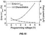
- the resultshows that the change in the OLED current due to a 2-volt VT-shift in the driving transistor (e.g. 14 of Figure 1 ) is almost zero percent for most of the programming voltage.
- Simulation parameters, such as threshold voltage,show that the shift has a high percentage at low programming voltage.
- FIG. 5illustrates a pixel circuit 202 having p-type transistors.
- the pixel circuit 202corresponds to the pixel circuit 200 of Figure 1 .
- the pixel circuit 202employs the CBVP driving scheme as shown in Figures 6-7 .
- the pixel circuit 202includes an OLED 20, a storage capacitor 22, a driving transistor 24, and switch transistors 26 and 28.
- the transistors 24, 26 and 28are p-type transistors. Each transistor has a gate terminal, a first terminal and a second terminal.
- the transistors 24, 26 and 28may be fabricated using amorphous silicon, nano/micro crystalline silicon, poly silicon, organic semiconductors technologies (e.g. organic TFTs), PMOS technology, or CMOS technology (e.g. MOSFET).
- a plurality of pixel circuits 202may form an AMOLED display array.
- Two select lines SEL1 and SEL2a signal line VDATA, a bias line IBIAS, a voltage supply line VDD, and a common ground are provided to the pixel circuit 202.
- the transistors 24 and 26 and the storage capacitor 22are connected to node A12.
- the cathode electrode of the OLED 20, the storage capacitor 22 and the transistors 24 and 28are connected to B12. Since the OLED cathode is connected to the other elements of the pixel circuit 202, this ensures integration with any OLED fabrication.
- Figure 6illustrates one exemplary operation process applied to the pixel circuit 202 of Figure 5 .
- Figure 6corresponds to Figure 2 .
- Figure 7illustrates a further exemplary operation process applied to the pixel circuit 202 of Figure 5 .
- Figure 7corresponds to Figure 3 .
- the CBVP driving schemes of Figures 6-7use IBIAS and VDATA similar to those of Figures 2-3 .
- FIG. 8illustrates a pixel circuit 204 in accordance with an example useful for understanding the present invention.
- the pixel circuit 204employs the CBVP driving scheme as described below.
- the pixel circuit 204 of Figure 8includes an OLED 30, storage capacitors 32 and 33, a driving transistor 34, and switch transistors 36, 38 and 40.
- Each of the transistors 34, 35 and 36includes a gate terminal, a first terminal and a second terminal. This pixel circuit 204 operates in the same way as that of the pixel circuit 200.
- the transistors 34, 36, 38 and 40are n-type TFT transistors.
- the driving technique applied to the pixel circuit 204is also applicable to a complementary pixel circuit having p-type transistors, as shown in Figure 10 .
- the transistors 34, 36, 38 and 40may be fabricated using amorphous silicon, nano/micro crystalline silicon, poly silicon, organic semiconductors technologies (e.g. organic TFTs), NMOS technology, or CMOS technology (e.g. MOSFET).
- a plurality of pixel circuits 204may form an AMOLED display array.
- a select line SEL, a signal line VDATA, a bias line IBIAS, a voltage line VDD, and a common groundare provided to the pixel circuit 204.
- the first terminal of the driving transistor 34is connected to the cathode electrode of the OLED 30.
- the second terminal of the driving transistor 34is connected to the ground.
- the gate terminal of the driving transistor 34is connected to its first terminal through the switch transistor 36.
- the storage capacitors 32 and 33are in series and connected between the gate of the driving transistor 34 and the ground.
- the gate terminal of the switch transistor 36is connected to the select line SEL.
- the first terminal of the switch transistor 36is connected to the first terminal of the driving transistor 34.
- the second terminal of the switch transistor 36is connected to the gate terminal of the driving transistor 34.
- the gate terminal of the switch transistor 38is connected to the select line SEL.
- the first terminal of the switch transistor 38is connected to the signal line VDATA.
- the second terminal of the switch transistor 38is connected to the connected terminal of the storage capacitors 32 and 33 (i.e. node C21).
- the gate terminal of the switch transistor 40is connected to the select line SEL.
- the first terminal of the switch transistor 40is connected to the bias line IBIAS.
- the second terminal of the switch transistor 40is connected to the cathode terminal of the OLED 30.
- the anode electrode of the OLED 30is connected to the VDD.
- the OLED 30, the transistors 34, 36 and 40are connected at node A21.
- the storage capacitor 32 and the transistors 34 and 36are connected at node B21.
- the operation of the pixel circuit 204includes a programming phase having a plurality of programming cycles, and a driving phase having one driving cycle.
- the programming phasethe first storage capacitor 32 is charged to a programming voltage VP plus the threshold voltage of the driving transistor 34, and the second storage capacitor 33 is charged to zero
- Figure 9illustrates one exemplary operation process applied to the pixel circuit 204 of Figure 8 .
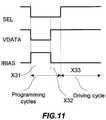
- the programming phasehas two operation cycles X31, X32, and the driving phase has one operation cycle X33.
- the first operation cycle X31The select line SEL is high.
- the second operation cycleWhile SEL is high, VDATA is zero, and IBIAS goes to zero. Because the capacitance 31 of the OLED 30 and the parasitic capacitance of the bias line IBIAS are large, the voltage of node B21 and the voltage of node A21 generated in the previous cycle stay unchanged.
- the gate-source voltage of the driving transistor 34is stored in the storage capacitor 32.
- the third operation cycle X33IBIAS goes to zero. SEL goes to zero. The voltage of node C21 goes to zero. The voltage stored in the storage capacitor 32 is applied to the gate terminal of the driving transistor 34. The gate-source voltage of the driving transistor 34 develops over the voltage stored in the storage capacitor 32. Considering that the current of driving transistor 34 is mainly defined by its gate-source voltage, the current through the OLED 30 becomes independent of the shifts of the threshold voltage of the driving transistor 34 and OLED characteristics.
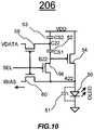
- Figure 10illustrates a pixel circuit 206 having p-type transistors.
- the pixel circuit 206corresponds to the pixel circuit 204 of Figure 8 .
- the pixel circuit 206employs the CBVP driving scheme as shown in Figure 11 .
- the pixel circuit 206 of Figure 10includes an OLED 50, a storage capacitors 52 and 53, a driving transistor 54, and switch transistors 56, 58 and 60.
- the transistors 54, 56, 58 and 60are p-type transistors. Each transistor has a gate terminal, a first terminal and a second terminal.
- the transistors 54, 56, 58 and 60may be fabricated using amorphous silicon, nano/micro crystalline silicon, poly silicon, organic semiconductors technologies (e.g. organic TFTs), PMOS technology, or CMOS technology (e.g. MOSFET).
- a plurality of pixel circuits 206may form an AMOLED display array.
- Two select lines SEL1 and SEL2a signal line VDATA, a bias line IBIAS, a voltage supply line VDD, and a common ground are provided to the pixel circuit 206.
- the common groundmay be same as that of Figure 1 .
- the anode electrode of the OLED 50, the transistors 54, 56 and 60are connected at node A22.
- the storage capacitor 52 and the transistors 54 and 56are connected at node B22.
- the switch transistor 58, and the storage capacitors 52 and 53are connected at node C22.
- Figure 11illustrates one exemplary operation process applied to the pixel circuit 206 of Figure 10 .
- Figure 11corresponds to Figure 9 .
- the CBVP driving scheme of Figure 11uses IBIAS and VDATA similar to those of Figure 9 .
- Figure 12illustrates a display 208 in accordance with an example useful for understanding the present invention.
- the display 208employs the CBVP driving scheme as described below.
- elements associated with two rows and one columnare shown as example.
- the display 208may include more than two rows and more than one column.
- the display 208includes an OLED 70, storage capacitors 72 and 73, transistors 76, 78, 80, 82 and 84.
- the transistor 76is a driving transistor.
- the transistors 78, 80 and 84are switch transistors.
- Each of the transistors 76, 78, 80, 82 and 84includes a gate terminal, a first terminal and a second terminal.
- the transistors 76, 78, 80, 82 and 84are n-type TFT transistors.
- the driving technique applied to the pixel circuit 208is also applicable to a complementary pixel circuit having p-type transistors, as shown in Figure 16 .
- the transistors 76, 78, 80, 82 and 84may be fabricated using amorphous silicon, nano/micro crystalline silicon, poly silicon, organic semiconductors technologies (e.g. organic TFTs), NMOS technology, or CMOS technology (e.g. MOSFET).
- the display 208may form an AMOLED display array. The combination of the CBVP driving scheme and the display 208 provides a large-area, high-resolution AMOLED display.
- the transistors 76 and 80 and the storage capacitor 72are connected at node A31.
- the transistors 82 and 84 and the storage capacitors 72 and 74are connected at B31.
- Figure 13illustrates one exemplary operation process applied to the display 208 of Figure 12 .
- "Programming cycle [n]”represents a programming cycle for the row [n] of the display 208.
- the programming timeis shared between two consecutive rows (n and n+1).
- SEL[n]is high, and a bias current IB is flowing through the transistors 78 and 80.
- VDATAchanges to VP-VB.
- the settling time of the CBVP pixel circuitis depicted in Figure 14 for different bias currents.
- a small currentcan be used as IB here, resulting in lower power consumption.
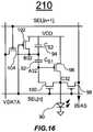
- Figure 16illustrates a display 210 having p-type transistors.
- the display 210corresponds to the display 208 of Figure 12 .
- the display 210employs the CBVP driving scheme as shown in Figure 17 .
- elements associated with two rows and one columnare shown as example.
- the display 210may include more than two rows and more than one column.
- the display 210includes an OLED 90, a storage capacitors 92 and 94, and transistors 96, 98, 100, 102 and 104.
- the transistor 96is a driving transistor.
- the transistors 100 and 104are switch transistors.
- the transistors 24, 26 and 28are p-type transistors. Each transistor has a gate terminal, a first terminal and a second terminal.
- the transistors 96, 98, 100, 102 and 104may be fabricated using amorphous silicon, nano/micro crystalline silicon, poly silicon, organic semiconductors technologies (e.g. organic TFTs), PMOS technology, or CMOS technology (e.g. MOSFET).
- the display 210may form an AMOLED display array.
- the driving transistor 96is connected between the anode electrode of the OLED 90 and a voltage supply line VDD.
- Figure 17illustrates one exemplary operation process applied to the display 210 of Figure 16 .
- Figure 17corresponds to Figure 13 .
- the CBVP driving scheme of Figure 17uses IBIAS and VDATA similar to those of Figure 13 .
- the overdrive voltage provided to the driving transistoris generated so as to be independent from its threshold voltage and the OLED voltage.
- the shift(s) of the characteristic(s) of a pixel element(s)is compensated for by voltage stored in a storage capacitor and applying it to the gate of the driving transistor.
- the pixel circuitcan provide a stable current though the light emitting device without any effect of the shifts, which improves the display operating lifetime.
- the circuit simplicitybecause of the circuit simplicity, it ensures higher product yield, lower fabrication cost and higher resolution than conventional pixel circuits.
- the settling time of the pixel circuits described aboveis much smaller than conventional pixel circuits, it is suitable for large-area display such as high definition TV, but it also does not preclude smaller display areas either.
- a driver for driving a display array having a CBVP pixel circuitconverts the pixel luminance data into voltage.
- VBCPvoltage-biased current-programmed
- FIG. 18illustrates a pixel circuit 212 in accordance with a further example useful for understanding the present invention.
- the pixel circuit 212employs the VBCP driving scheme as described below.
- the pixel circuit 212 of Figure 18includes an OLED 110, a storage capacitor 111, a switch network 112, and mirror transistors 114 and 116.
- the mirror transistors 114 and 116form a current mirror.
- the transistor 114is a programming transistor.
- the transistor 116is a driving transistor.
- the switch network 112includes switch transistors 118 and 120. Each of the transistors 114, 116, 118 and 120 has a gate terminal, a first terminal and a second terminal.
- the transistors 114, 116, 118 and 120are n-type TFT transistors.
- the driving technique applied to the pixel circuit 212is also applicable to a complementary pixel circuit having p-type transistors as shown in Figure 20 .
- the transistors 114, 116, 118 and 120may be fabricated using amorphous silicon, nano/micro crystalline silicon, poly silicon, organic semiconductors technologies (e.g. organic TFTs), NMOS technology, or CMOS technology (e.g. MOSFET).
- a plurality of pixel circuits 212may form an AMOLED display array.
- a select line SEL, a signal line IDATA, a virtual grand line VGND, a voltage supply line VDD, and a common groundare provided to the pixel circuit 150.
- the first terminal of the transistor 116is connected to the cathode electrode of the OLED 110.
- the second terminal of the transistor 116is connected to the VGND.
- the gate terminal of the transistor 114, the gate terminal of the transistor 116, and the storage capacitor 111are connected to a connection node A41.
- the gate terminals of the switch transistors 118 and 120are connected to the SEL.
- the first terminal of the switch transistor 120is connected to the IDATA.
- the switch transistors 118 and 120are connected to the first terminal of the transistor 114.
- the switch transistor 118is connected to node A41.
- Figure 19illustrates an exemplary operation for the pixel circuit 212 of Figure 18 .
- current scaling technique applied to the pixel circuit 212is described in detail.
- the operation of the pixel circuit 212has a programming cycle X41, and a driving cycle X42.
- the programming cycle X41: SELis high. Thus, the switch transistors 118 and 120 are on.
- the VGNDgoes to a bias voltage VB.
- a current (IB+IP)is provided through the IDATA, where IP represents a programming current, and IB represents a bias current.
- a current equal to (IB+IP)passes through the switch transistors 118 and 120.
- IDSrepresents the drain-source current of the driving transistor 116.
- VCSIP + IB ⁇ ⁇ VB + VT
- VCSrepresents the voltage stored in the storage capacitor 111.
- IpixelIP + IB + ⁇ ⁇ VB 2 ⁇ 2 ⁇ ⁇ VB ⁇ IP + IB where Ipixel represents the pixel current flowing through the OLED 110.
- IpixelIP + IB + ⁇ ⁇ VB 2 ⁇ 2 ⁇ ⁇ VB ⁇ IB
- VBIB ⁇
- the pixel current Ipixelbecomes equal to the programming current IP. Therefore, it avoids unwanted emission during the programming cycle.
- Figure 20illustrates a pixel circuit 214 having p-type transistors.
- the pixel circuit 214corresponds to the pixel circuit 212 of Figure 18 .
- the pixel circuit 214employs the VBCP driving scheme as shown Figure 21 .
- the pixel circuit 214includes an OLED 130, a storage capacitor 131, a switch network 132, and mirror transistors 134 and 136.
- the mirror transistors 134 and 136form a current mirror.
- the transistor 134is a programming transistor.
- the transistor 136is a driving transistor.
- the switch network 132includes switch transistors 138 and 140.
- the transistors 134, 136, 138 and 140are p-type TFT transistors. Each of the transistors 134, 136, 138 and 140 has a gate terminal, a first terminal and a second terminal.
- the transistors 134, 136, 138 and 140may be fabricated using amorphous silicon, nano/micro crystalline silicon, poly silicon, organic semiconductors technologies (e.g. organic TFTs), PMOS technology, or CMOS technology (e.g. MOSFET).
- a plurality of pixel circuits 214may form an AMOLED display array.
- a select line SEL, a signal line IDATA, a virtual grand line VGND, and a voltage supply line VSSare provided to the pixel circuit 214.
- the transistor 136is connected between the VGND and the cathode electrode of the OLED 130.
- the gate terminal of the transistor 134, the gate terminal of the transistor 136, the storage capacitor 131 and the switch network 132are connected at node A42.
- Figure 21illustrates an exemplary operation for the pixel circuit 214 of Figure 20 .
- Figure 21corresponds to Figure 19 .
- the VBCP driving scheme of Figure 21uses IDATA and VGND similar to those of Figure 19 .
- the VBCP technique applied to the pixel circuit 212 and 214is applicable to current programmed pixel circuits other than current mirror type pixel circuit.
- the VBCP techniqueis suitable for the use in AMOLED displays.
- the VBCP techniqueenhances the settling time of the current-programmed pixel circuits display, e.g. AMOLED displays.
- a driver for driving a display array having a VBCP pixel circuitconverts the pixel luminance data into current.
- FIG 22illustrates a driving mechanism for a display array 150 having a plurality of CBVP pixel circuits 151 (CBVP1-1, CBVP1-2, CBVP2-1, CBVP2-2).
- the CBVP pixel circuit 151is a pixel circuit to which the CBVP driving scheme is applicable.
- the CBVP pixel circuit 151may be the pixel circuit shown in Figure 1 , 5 , 8 , 10 , 12 or 16 .
- four CBVP pixel circuits 151are shown as example.
- the display array 150may have more than four or less than four CBVP pixel circuits 151.
- the display array 150is an AMOLED display where a plurality of the CBVP pixel circuits 151 are arranged in rows and columns.
- VDATA1(or VDATA 2) and IBIAS1 (or IBIAS2) are shared between the common column pixels while SEL1 (or SEL2) is shared between common row pixels in the array structure.
- the SEL1 and SEL2are driven through an address driver 152.
- the VDATA1 and VDATA2are driven through a source driver 154.
- the IBIAS1 and IBIAS2are also driven through the source driver 154.
- a controller and scheduler 156is provided for controlling and scheduling programming, calibration and other operations for operating the display array, which includes the control and schedule for the CBVP driving scheme as described above.
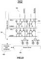
- Figure 23illustrates a driving mechanism for a display array 160 having a plurality of VBCP pixel circuits.
- the pixel circuit 212 of Figure 18is shown as an example of the VBCP pixel circuit.
- the display array 160may include any other pixel circuits to which the VBCP driving scheme described is applicable.
- SEL1 and SEL2 of Figure 23correspond to SEL of Figure 18 .
- VGND1 and VGAND2 of Figure 23correspond to VDATA of Figure 18 .
- IDATA1 and IDATA 2 of Figure 23correspond to IDATA of Figure 18 .
- four VBCP pixel circuitsare shown as example.
- the display array 160may have more than four or less than four VBCP pixel circuits.
- the display array 160is an AMOLED display where a plurality of the VBCP pixel circuits are arranged in rows and columns. IDATA1 (or IDATA2) is shared between the common column pixels while SEL1 (or SEL2) and VGND1 (or VGND2) are shared between common row pixels in the array structure.
- the SEL1, SEL2, VGND1 and VGND2are driven through an address driver 162.
- the IDATA1 and IDATAare driven through a source driver 164.
- a controller and scheduler 166is provided for controlling and scheduling programming, calibration and other operations for operating the display array, which includes the control and schedule for the VBCP driving scheme as described above.
- Figure 24illustrates a pixel circuit 400 in accordance with a further example useful for understanding the present invention.
- the pixel circuit 400 of Figure 24is a 3-TFT current-biased voltage programmed pixel circuit and employs the CBVP driving scheme.
- the driving schemeimproves the display lifetime and yield by compensating for the mismatches.
- the pixel circuit 400includes an OLED 402, a storage capacitor 404, a driving transistor 406, and switch transistors 408 and 410. Each transistor has a gate terminal, a first terminal and a second terminal.
- the transistors 406, 408 and 410are p-type TFT transistors.
- the driving technique applied to the pixel circuit 400is also applicable to a complementary pixel circuit having n-type transistors as well understood by one of ordinary skill in the art.
- the transistors 406, 408 and 410may be implemented using poly silicon, nano/micro (crystalline) silicon, amorphous silicon, CMOS, organic semiconductor, metal organic technologies, or combination thereof.
- a plurality of pixel circuits 400may form an active matrix array. The driving scheme applied to the pixel circuit 400 compensates for temporal and spatial non-uniformities in the active matrix display.
- a select line SET, a signal line Vdata, a bias line Ibias, and a voltage supply line Vddare connected to the pixel circuit 400.
- the bias line Ibiasprovides a bias current (Ibias) that is defined based on display specifications, such as lifetime, power, and device performance and uniformity.
- the first terminal of the driving transistor 406is connected to the voltage supply line Vdd.
- the second terminal of the driving transistor 406is connected to the OLED 402 at node B20.
- One terminal of the capacitor 404is connected to the signal line Vdata, and the other terminal of the capacitor 404 is connected to the gate terminal of the driving transistor 406 at node A20.
- the gate terminals of the switch transistors 408 and 410are connected to the select line SEL.
- the switch transistor 408is connected between node A20 and node B20.
- the switch transistor 410is connected between the node B20 and the bias line Ibias.
- a predetermined fixed current(Ibias) is provided through the transistor 410 to compensate for all spatial and temporal non-uniformities and voltage programming is used to divide the current in different current levels required for different gray scales.
- the operation of the pixel circuit 400includes a programming phase X61 and a driving phase X62.
- Vdata [j] of Figure 25corresponds to Vdd of Figure 24 .
- SELis low so that the switch transistors 408 and 410 are on.
- the bias current Ibiasis applied via the bias line Ibias to the pixel circuit 400, and the gate terminal of the driving transistor 406 is self-adjusted to allow all the current passes through source-drain of the driving transistor 406.
- Vdatahas a programming voltage related to the gray scale of the pixel.
- the switch transistors 408 and 410are off, and the current passes through the driving transistor 406 and the OLED 402.
- Figure 26is a diagram showing a pixel circuit 420 in accordance with a further embodiment of the present invention.
- the pixel circuit 420 of Figure 26is a 6-TFT current-biased voltage programmed pixel circuit and employs the CBVP driving scheme, with emission control. This driving scheme improves the display lifetime and yield by compensating for the mismatches.
- the pixel circuit 420includes an OLED 422, a storage capacitor 424, and transistors 426-436. Each transistor has a gate terminal, a first terminal and a second terminal.
- the transistors 426-436are p-type TFT transistors.
- the driving technique applied to the pixel circuit 420is also applicable to a complementary pixel circuit having n-type transistors as well understood by one of ordinary skill in the art.
- the transistors 426-436may be implemented using poly silicon, nano/micro (crystalline) silicon, amorphous silicon, CMOS, organic semiconductor, metal organic technologies, or combination thereof.
- a plurality of pixel circuits 420may form an active matrix array. The driving scheme applied to the pixel circuit 420 compensates for temporal and spatial non-uniformities in the active matrix display.
- the bias line Ibiasprovides a bias current (Ibias) that is defined based on display specifications, such as lifetime, power, and device performance and uniformity.
- the reference voltage line Vrefprovides a reference voltage (Vref). The reference voltage Vref may be determined based on the bias current Ibias and the display specifications that may include gray scale and/or contrast ratio.
- the signal line EMprovides an emission signal EM that turns on the pixel circuit 420. The pixel circuit 420 goes to emission mode based on the emission signal EM.
- the gate terminal of the transistor 426, one terminal of the transistor 432 and one terminal of the transistor 434are connected at node A21.
- One terminal of the capacitor 424, one terminal of the transistor 428 and the other terminal of the transistor 434are connected at node B21.
- the other terminal of the capacitor 424, one terminal of the transistor 430, one terminal of the transistor 436, and one terminal of the transistor 426are connected at node C21.
- the other terminal of the transistor 430is connected to the bias line Ibias.
- the other terminal of the transistor 432is connected to the reference voltage line Vref.
- the select line SELis connected to the gate terminals of the transistors 428, 430 and 432.
- the select line EMis connected to the gate terminals of the transistors 434, and 436.
- the transistor 426is a driving transistor.
- the transistors 428, 430, 432, 434, and 436are switching transistors.
- a predetermined fixed current(Ibias) is provided through the transistor 430 while the reference voltage Vref is applied to the gate terminal of the transistor 426 through the transistor 432 and a programming voltage VP is applied to the other terminal of the storage capacitor 424 (i.e., node B21) through the transistor 428.
- the source voltage of the transistor 426i.e., voltage of node C21
- voltage programmingis used to divide the current in different current levels required for different gray scales.
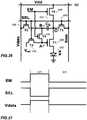
- the operation of the pixel circuit 420includes a programming phase X71 and a driving phase X72.
- SELis low so that the transistors 428, 430 and 432 are on, a fixed bias current is applied to Ibias line, and the source of the transistor 426 is self-adjusted to allow all the current passes through source-drain of the transistor 426.
- Vdatahas a programming voltage related to the gray scale of the pixel and the capacitor 424 stores the programming voltage and the voltage generated by current for mismatch compensation.
- the transistors 428, 430 and 432are off, while the transistors 434 and 436 are on by the emission signal EM.
- the transistor 426provides current for the OLED 422.
- each rowcan light up after programming by using the emission line EM.
- the bias lineprovides a predetermined fixed bias current.
- the bias current Ibiasmay be adjustable, and the bias current Ibias may be adjusted during the operation of the display.
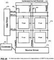
- FIG 28illustrates an example of a display system having array structure for implementation of the CBVP driving scheme.
- the display system 450 of Figure 28includes a pixel array 452 having a plurality of pixels 454, a gate driver 456, a source driver 458 and a controller 460 for controlling the drivers 456 and 458.
- the gate driver 456operates on address (select) lines (e.g., SEL [1], SEL[2], ).
- the source driver 458operates on data lines (e.g., Vdata [1], Vdata [2], ).
- the display system 450includes a calibrated current mirrors block 462 for operating on bias lines (e.g., Ibias [1], Ibias [2]) using a reference current Iref.
- the block 462includes a plurality of calibrated current mirrors, each for the corresponding Ibias.
- the reference current Irefmay be provided to the calibrated current mirrors block 462 through a switch.
- a driver at the peripheral of the displaysuch as the gate driver 456, controls each emission line EM.
- the current mirrorsare calibrated with a reference current source.
- the calibrated current mirrors(block 462) provide current to the bias line Ibias. These current mirrors can be fabricated at the edge of the panel.
- FIG 29illustrates another example of a display system having array structure for implementation of the CBVP driving scheme.
- the display system 470 of Figure 29includes a pixel array 472 having a plurality of pixels 474, a gate driver 476, a source driver 478 and a controller 480 for controlling the drivers 476 and 478.
- the gate driver 476operates on address (select) lines (e.g., SEL[0], SEL [1], SEL[2], ).
- the source driver 478operates on data lines (e.g., Vdata [1], Vdata [2], ).
- the display system 470includes a calibrated current sources block 482 for operating on bias lines (e.g., Ibias [1], Ibias [2]) using Vdata lines.
- the block 482includes a plurality of calibrated current sources, each being provided for the Ibias line.
- a driver at the peripheral of the displaysuch as the gate driver 456, controls each emission line EM.
- Each current source 482includes a voltage to current convertor that converts voltage via Vdata line to current.
- One of the select linesis used to operate a switch 490 for connecting Vdata line to the current source 482.
- address line SEL [0]operates the switch 490.
- the current sources 482are treated as one row of the display (i.e., the 0 th row). After the conversion of voltage on Vdata line at the current source 482, Vdata line is used to program the real pixel circuits 474 of the display.
- a voltage related to each of the current sourcesis extracted at the factory and is stored in a memory (e.g. flash, EPROM, or PROM). This voltage (calibrated voltage) may be different for each current source due to their mismatches.
- the current sources 482are programmed through the source driver 478 using the stored calibrated voltages so that all the current sources 482 provides the same current.
- the bias current (Ibias)is generated by the current mirror 462 with the reference current Iref.
- the system 450 of Figure 28may use the current source 482 to generate Ibias.
- the bias current (Ibias)is generated by the current converter of the current source 482 with Vdata line.
- the system 470 of Figure 29may use the current mirror 462 of Figure 28 .
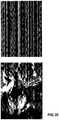
- FIGs 30-32Effect of spatial mismatches on the image quality of panels using different driving scheme is depicted in Figures 30-32 .
- the image of display with conventional 2-TFT pixel circuitis suffering from both threshold voltage mismatches and mobility variations ( Figure 30 ).
- the voltage programmed pixel circuits without the bias line Ibiasmay control the effect of threshold voltage mismatches, however, they may suffer from the mobility variations ( Figure 31 ) whereas the current-biased voltage-programmed (CBVP) driving scheme in the embodiments can control the effect of both mobility and threshold voltage variations ( Figure 32 ).
- CBVPcurrent-biased voltage-programmed
Landscapes
- Engineering & Computer Science (AREA)
- Physics & Mathematics (AREA)
- Computer Hardware Design (AREA)
- General Physics & Mathematics (AREA)
- Theoretical Computer Science (AREA)
- Control Of Indicators Other Than Cathode Ray Tubes (AREA)
- Electroluminescent Light Sources (AREA)
- Control Of El Displays (AREA)
- Transforming Electric Information Into Light Information (AREA)
Description
- The present invention relates to a light emitting device displays, and more specifically to a driving technique for the light emitting device displays.
- Recently active-matrix organic light-emitting diode (AMOLED) displays with amorphous silicon (a-Si), poly-silicon, organic, or other driving backplane technology have become more attractive due to advantages over active matrix liquid crystal displays. An AMOLED display using a-Si backplanes, for example, has the advantages which include low temperature fabrication that broadens the use of different substrates and makes flexible displays feasible, and its low cost fabrication is well-established and yields high resolution displays with a wide viewing angle.
- An AMOLED display includes an array of rows and columns of pixels, each having an organic light-emitting diode (OLED) and backplane electronics arranged in the array of rows and columns. Since the OLED is a current driven device, the pixel circuit of the AMOLED should be capable of providing an accurate and constant drive current.
- One method that has been employed to drive the AMOLED display is programming the AMOLED pixel directly with current. However, the small current required by the OLED, coupled with a large parasitic capacitance, undesirably increases the settling time of the programming of the current-programmed AMOLED display. Furthermore, it is difficult to design an external driver to accurately supply the required current. For example, in CMOS technology, the transistors must work in sub-threshold regime to provide the small current required by the OLEDs, which is not ideal. Therefore, in order to use current-programmed AMOLED pixel circuits, suitable driving schemes are desirable.
- Current scaling is one method that can be used to manage issues associated with the small current required by the OLEDs. In a current mirror pixel circuit, the current passing through the OLED can be scaled by having a smaller drive transistor as compared to the mirror transistor. However, this method is not applicable for other current-programmed pixel circuits. Also, by resizing the two mirror transistors the effect of mismatch increases.
- Patent application publication
CA 2523841 A provides an active matrix light emitting device display and its driving technique is provided. The pixel includes a light emitting device and a plurality of transistors. A capacitor may be used to store a voltage applied to a driving transistor so that a current through the light emitting device is independent of any shifts of the transistor and light emitting device characteristics. A bias data and a programming data are provided to the pixel circuit in accordance with a driving scheme. - Patent application publication
US 2006/145967 A relates to an organic electro-luminescence device that includes a drive unit having first to fourth transistors and a capacitor, and an organic light emitting diode (OLED) controlled by the drive unit, wherein the first transistor has its gate, drain and source connected to a first node, a second node and a power voltage supply line, respectively; the second transistor has its drain and source connected to the OLED and the second node, respectively; the third transistor has its gate, drain and source connected to a first select signal line, the second node and the first node, respectively; the fourth transistor has its gate, drain and source connected to the first select signal line, a data line, and the second node, respectively; and the capacitor is connected to the first node and a predetermined signal line. - Patent application publication
US 2006/0077194 A1 describes another pixel circuit of an active matrix OLED display addressing transistor threshold voltage variations and voltage drop on the power supply lines. The pixel circuit comprises a first switching transistor (M1) connecting the data line (Dm) to a first node (A) in response to a first scan line signal (S1.n), a fourth switching transistor (M5) connecting the pixel power line (Vdd) to a third node (C) in response to a third scan line signal (S3.n), a capacitor (Cst) connected between the first node (A) and the third node (C), a third switching transistor (M3) connecting the first node (A) to a second node (B) in response to a second scan line signal (S2.n), a driving transistor (M4) for supplying current from the third node (C) to an OLED according to the voltage of the second node (B) applied to its gate electrode, a second switching transistor (M2) supplying a compensation power (Vinit) to the second node (B) in response to the first scan line signal (S1.n), and a fifth switching transistor(M6) short-circuiting the OLED in response to the third scan line signal (S3.n). - It is an object of the invention to provide a pixel circuit and a display system comprising same that obviate or mitigate at least one of the disadvantages of existing systems.
- This object is solved by the present invention as claimed in the appended independent claims. Advantageous embodiments of the present invention are defined by the appended dependent claims.
- In accordance with a comparative example there is provided a pixel circuit, which includes a light emitting device, a driving transistor for providing a pixel current to the light emitting device, a storage capacitor provided between a data line for providing programming voltage data and the gate terminal of the driving transistor, a first switch transistor provided between the gate terminal of the driving transistor and the light emitting device, and a second switch transistor provided between the light emitting device and a bias line for providing a bias current to the first terminal of the driving transistor during a programming cycle.
- In accordance with a further comparative example there is provided a pixel circuit, which includes a light emitting device, a storage capacitor, a driving transistor for providing a pixel current to the light emitting device, a plurality of first switch transistors operated by a first select line, one of the first switch transistors being provided between the storage capacitor and a data line for providing programming voltage data, a plurality of second switch transistors operated by a second select line, one of the second switch transistor being provided between the driving transistor and a bias line for providing a bias current to the first terminal of the driving transistor during a programming cycle; and an emission control circuit for setting the pixel circuit into an emission mode.
- In accordance with a further comparative example there is provided a display system, which includes a pixel array having a plurality of pixel circuits, a first driver for selecting the pixel circuit, a second driver for providing the programming voltage data, and a current source for operating on the bias line.
- In accordance with a further comparative example there is provided a method of driving a pixel circuit, the pixel circuit having a driving transistor for providing a pixel current to a light emitting device, a storage capacitor coupled
to a data line, and a switch transistor coupled to the gate terminal of the driving transistor and the storage capacitor. The method includes:at a programming cycle, selecting the pixel circuit, providing a bias current to a connection between the driving transistor and the light emitting device, and providing programming voltage data from the data line to the pixel circuit. - In accordance with a further comparative example there is provided a method of driving a pixel circuit, the pixel circuit having a driving transistor for providing a pixel current to a light emitting device, a switch transistor coupled to a data line, and a storage capacitor coupled to the switch transistor and the driving transistor. The method includes: at a programming cycle, selecting the pixel circuit, providing a bias current to a first terminal of the driving transistor, and providing programming voltage data from the data line to a first terminal of the storage capacitor, the second terminal of the storage capacitor being coupled to the first terminal of the driving transistor, a second terminal of the driving transistor being coupled to the light emitting device; and at a driving cycle, setting an emission mode in the pixel circuit.
- This summary of the invention does not necessarily describe all features of the invention.
- Other aspects and features of the present invention will be readily apparent to those skilled in the art from a review of the following detailed description of preferred embodiments in conjunction with the accompanying drawings.
- These and other features of the invention will become more apparent from the following description in which reference is made to the appended drawings wherein:
Figure 1 is a diagram showing a pixel circuit in accordance with an example useful for understanding the present invention;Figure 2 is a timing diagram showing exemplary waveforms applied to the pixel circuit ofFigure 1 ;Figure 3 is a timing diagram showing further exemplary waveforms applied to the pixel circuit ofFigure 1 ;Figure 4 is a graph showing a current stability of the pixel circuit ofFigure 1 ;Figure 5 is a diagram showing a pixel circuit which has p-type transistors and corresponds to the pixel circuit ofFigure 1 ;Figure 6 is a timing diagram showing exemplary waveforms applied to the pixel circuit ofFigure 5 ;Figure 7 is a timing diagram showing further exemplary waveforms applied to the pixel circuit ofFigure 5 ;Figure 8 is a diagram showing a pixel circuit in accordance with a further example useful for understanding the present invention;Figure 9 is a timing diagram showing exemplary waveforms applied to the pixel circuit ofFigure 8 ;Figure 10 is a diagram showing a pixel circuit which has p-type transistors and corresponds to the pixel circuit ofFigure 8 ;Figure 11 is a timing diagram showing exemplary waveforms applied to the pixel circuit ofFigure 10 ;Figure 12 is a diagram showing a pixel circuit in accordance with an example useful for understanding the present invention;Figure 13 is a timing diagram showing exemplary waveforms applied to the display ofFigure 12 ;Figure 14 is a graph showing the settling time of a CBVP pixel circuit for different bias currents;Figure 15 is a graph showing I-V characteristic of the CBVP pixel circuit as well as the total error induced in the pixel current;Figure 16 is a diagram showing a pixel circuit which has p-type transistors and corresponds to the pixel circuit ofFigure 12 ;Figure 17 is a timing diagram showing exemplary waveforms applied to the display ofFigure 16 ;Figure 18 is a diagram showing a VBCP pixel circuit in accordance with a further example useful for understanding the present invention;Figure 19 is a timing diagram showing exemplary waveforms applied to the pixel circuit ofFigure 18 ;Figure 20 is a diagram showing a VBCP pixel circuit which has p-type transistors and corresponds to the pixel circuit ofFigure 18 ;Figure 21 is a timing diagram showing exemplary waveforms applied to the pixel circuit ofFigure 20 ;Figure 22 is a diagram showing a driving mechanism for a display array having CBVP pixel circuits;Figure 23 is a diagram showing a driving mechanism for a display array having VBCP pixel circuits;Figure 24 is a diagram showing a pixel circuit in accordance with a further example useful for understanding the present invention;Figure 25 is a timing diagram showing exemplary waveforms applied to the pixel circuit ofFigure 24 ;Figure 26 is a diagram showing a pixel circuit in accordance with an embodiment of the present invention;Figure 27 is a timing diagram showing exemplary waveforms applied to the pixel circuit ofFigure 26 ;Figure 28 is a diagram showing a further example of a display system having CBVP pixel circuits;Figure 29 is a diagram showing a further example of a display system having CBVP pixel circuits;Figure 30 is a photograph showing effect of spatial mismatches on a display using a simple 2-TFT pixel circuit;Figure 31 is a photograph showing effect of spatial mismatches on a display using the voltage-programmed circuits; andFigure 32 is a photograph showing effect of spatial mismatches on a display using CBVP pixel circuit.- Embodiments of the present invention are described using a pixel having an organic light emitting diode (OLED) and a driving thin film transistor (TFT). However, the pixel may include any light emitting device other than OLED, and the pixel may include any driving transistor other than TFT. It is noted that in the description, "pixel circuit" and "pixel" may be used interchangeably.
- A driving technique for pixels, including a current-biased voltage-programmed (CBVP) driving scheme, is now described in detail. The CBVP driving scheme uses voltage to provide for different gray scales (voltage programming), and uses a bias to accelerate the programming and compensate for the time dependent parameters of a pixel, such as a threshold voltage shift and OLED voltage shift.
Figure 1 illustrates apixel circuit 200 in accordance with an example useful for understanding the present invention. Thepixel circuit 200 employs the CBVP driving scheme as described below. Thepixel circuit 200 ofFigure 1 includes anOLED 10, astorage capacitor 12, a drivingtransistor 14, and switchtransistors - The
transistors pixel circuit 200 is also applicable to a complementary pixel circuit having p-type transistors as shown inFigure 5 . - The
transistors pixel circuits 200 may form an AMOLED display array. - Two select lines SEL1 and SEL2, a signal line VDATA, a bias line IBIAS, a voltage supply line VDD, and a common ground are provided to the
pixel circuit 200. InFigure 1 , the common ground is for the OLED top electrode. The common ground is not a part of the pixel circuit, and is formed at the final stage when theOLED 10 is formed. - The first terminal of the driving
transistor 14 is connected to the voltage supply line VDD. The second terminal of the drivingtransistor 14 is connected to the anode electrode of theOLED 10. The gate terminal of the drivingtransistor 14 is connected to the signal line VDATA through theswitch transistor 16. Thestorage capacitor 12 is connected between the second and gate terminals of the drivingtransistor 14. - The gate terminal of the
switch transistor 16 is connected to the first select line SEL1. The first terminal of theswitch transistor 16 is connected to the signal line VDATA. The second terminal of theswitch transistor 16 is connected to the gate terminal of the drivingtransistor 14. - The gate terminal of the
switch transistor 18 is connected to the second select line SEL2. The first terminal oftransistor 18 is connected to the anode electrode of theOLED 10 and thestorage capacitor 12. The second terminal of theswitch transistor 18 is connected to the bias line IBIAS. The cathode electrode of theOLED 10 is connected to the common ground. - The
transistors storage capacitor 12 are connected to node A11. TheOLED 10, thestorage capacitor 12 and thetransistors - The operation of the
pixel circuit 200 includes a programming phase having a plurality of programming cycles, and a driving phase having one driving cycle. During the programming phase, node B11 is charged to negative of the threshold voltage of the drivingtransistor 14, and node A11 is charged to a programming voltage VP. - As a result, the gate-source voltage of the driving
transistor 14 is:
transistor 14, and VT represents the threshold voltage of the drivingtransistor 14. This voltage remains on thecapacitor 12 in the driving phase, resulting in the flow of the desired current through theOLED 10 in the driving phase. - The programming and driving phases of the
pixel circuit 200 are described in detail.Figure 2 illustrates one exemplary operation process applied to thepixel circuit 200 ofFigure 1 . InFigure 2 , VnodeB represents the voltage of node B11, and VnodeA represents the voltage of node A11. As shown inFigure 2 , the programming phase has two operation cycles X11, X12, and the driving phase has one operation cycle X13. - The first operation cycle X11: Both select lines SEL1 and SEL2 are high. A bias current IB flows through the bias line IBIAS, and VDATA goes to a bias voltage VB.
- As a result, the voltage of node B11 is:

transistor 14, and β represents the coefficient in current-voltage (I-V) characteristics of the TFT given by IDS = β (VGS - VT)2. IDS represents the drain-source current of the drivingtransistor 14. - The second operation cycle X12: While SEL2 is low, and SEL1 is high, VDATA goes to a programming voltage VP. Because the
capacitance 11 of theOLED 20 is large, the voltage of node B11 generated in the previous cycle stays intact. - Therefore, the gate-source voltage of the driving
transistor 14 can be found as:

- ΔVB is zero when VB is chosen properly based on (4). The gate-source voltage of the driving
transistor 14, i.e., VP+VT, is stored in thestorage capacitor 12. - The third operation cycle X13: IBIAS goes to low. SEL1 goes to zero. The voltage stored in the
storage capacitor 12 is applied to the gate terminal of the drivingtransistor 14. The drivingtransistor 14 is on. The gate-source voltage of the drivingtransistor 14 develops over the voltage stored in thestorage capacitor 12. Thus, the current through theOLED 10 becomes independent of the shifts of the threshold voltage of the drivingtransistor 14 and OLED characteristics. Figure 3 illustrates a further exemplary operation process applied to thepixel circuit 200 ofFigure 1 . InFigure 3 , VnodeB represents the voltage of node B11, and VnodeA represents the voltage of node A11.- The programming phase has two operation cycles X21, X22, and the driving phase has one operation cycle X23. The first operation cycle X21 is same as the first operation cycle X11 of
Figure 2 . The third operation cycle X33 is same as the thirdoperation cycle X 13 ofFigure 2 . InFigure 3 , the select lines SEL1 and SEL2 have the same timing. Thus, SEL1 and SEL2 may be connected to a common select line. - The second operating cycle X22: SEL1 and SEL2 are high. The
switch transistor 18 is on. The bias current IB flowing through IBIAS is zero. - The gate-source voltage of the driving
transistor 14 can be VGS = VP + VT as described above. The gate-source voltage of the drivingtransistor 14, i.e., VP+VT, is stored in thestorage capacitor 12. Figure 4 illustrates a simulation result for thepixel circuit 200 ofFigure 1 and the waveforms ofFigure 2 . The result shows that the change in the OLED current due to a 2-volt VT-shift in the driving transistor (e.g. 14 ofFigure 1 ) is almost zero percent for most of the programming voltage. Simulation parameters, such as threshold voltage, show that the shift has a high percentage at low programming voltage.Figure 5 illustrates apixel circuit 202 having p-type transistors. Thepixel circuit 202 corresponds to thepixel circuit 200 ofFigure 1 . Thepixel circuit 202 employs the CBVP driving scheme as shown inFigures 6-7 . Thepixel circuit 202 includes anOLED 20, astorage capacitor 22, a drivingtransistor 24, and switchtransistors transistors - The
transistors pixel circuits 202 may form an AMOLED display array. - Two select lines SEL1 and SEL2, a signal line VDATA, a bias line IBIAS, a voltage supply line VDD, and a common ground are provided to the
pixel circuit 202. - The
transistors storage capacitor 22 are connected to node A12. The cathode electrode of theOLED 20, thestorage capacitor 22 and thetransistors pixel circuit 202, this ensures integration with any OLED fabrication. Figure 6 illustrates one exemplary operation process applied to thepixel circuit 202 ofFigure 5 .Figure 6 corresponds toFigure 2 .Figure 7 illustrates a further exemplary operation process applied to thepixel circuit 202 ofFigure 5 .Figure 7 corresponds toFigure 3 . The CBVP driving schemes ofFigures 6-7 use IBIAS and VDATA similar to those ofFigures 2-3 .Figure 8 illustrates apixel circuit 204 in accordance with an example useful for understanding the present invention. Thepixel circuit 204 employs the CBVP driving scheme as described below. Thepixel circuit 204 ofFigure 8 includes anOLED 30,storage capacitors transistors transistors 34, 35 and 36 includes a gate terminal, a first terminal and a second terminal. Thispixel circuit 204 operates in the same way as that of thepixel circuit 200.- The
transistors pixel circuit 204 is also applicable to a complementary pixel circuit having p-type transistors, as shown inFigure 10 . - The
transistors pixel circuits 204 may form an AMOLED display array. - A select line SEL, a signal line VDATA, a bias line IBIAS, a voltage line VDD, and a common ground are provided to the
pixel circuit 204. - The first terminal of the driving transistor 34 is connected to the cathode electrode of the
OLED 30. The second terminal of the driving transistor 34 is connected to the ground. The gate terminal of the driving transistor 34 is connected to its first terminal through theswitch transistor 36. Thestorage capacitors - The gate terminal of the
switch transistor 36 is connected to the select line SEL. The first terminal of theswitch transistor 36 is connected to the first terminal of the driving transistor 34. The second terminal of theswitch transistor 36 is connected to the gate terminal of the driving transistor 34. - The gate terminal of the
switch transistor 38 is connected to the select line SEL. The first terminal of theswitch transistor 38 is connected to the signal line VDATA. The second terminal of theswitch transistor 38 is connected to the connected terminal of thestorage capacitors 32 and 33 (i.e. node C21). - The gate terminal of the
switch transistor 40 is connected to the select line SEL. The first terminal of theswitch transistor 40 is connected to the bias line IBIAS. The second terminal of theswitch transistor 40 is connected to the cathode terminal of theOLED 30. The anode electrode of theOLED 30 is connected to the VDD. - The
OLED 30, thetransistors storage capacitor 32 and thetransistors 34 and 36 are connected at node B21. - The operation of the
pixel circuit 204 includes a programming phase having a plurality of programming cycles, and a driving phase having one driving cycle. During the programming phase, thefirst storage capacitor 32 is charged to a programming voltage VP plus the threshold voltage of the driving transistor 34, and thesecond storage capacitor 33 is charged to zero - As a result, the gate-source voltage of the driving transistor 34 is:

- The programming and driving phases of the
pixel circuit 204 are described in detail.Figure 9 illustrates one exemplary operation process applied to thepixel circuit 204 ofFigure 8 . As shown inFigure 9 , the programming phase has two operation cycles X31, X32, and the driving phase has one operation cycle X33. - The first operation cycle X31: The select line SEL is high. A bias current IB flows through the bias line IBIAS, and VDATA goes to a VB-VP where VP is and programming voltage and VB is given by:

- As a result, the voltage stored in the
first capacitor 32 is:
first storage capacitor 32, VT represents the threshold voltage of the driving transistor 34, β represents the coefficient in current-voltage (I-V) characteristics of the TFT given by IDS = β(VGS-VT)2. IDS represents the drain-source current of the driving transistor 34. - The second operation cycle: While SEL is high, VDATA is zero, and IBIAS goes to zero. Because the
capacitance 31 of theOLED 30 and the parasitic capacitance of the bias line IBIAS are large, the voltage of node B21 and the voltage of node A21 generated in the previous cycle stay unchanged. - Therefore, the gate-source voltage of the driving transistor 34 can be found as:

- The gate-source voltage of the driving transistor 34 is stored in the
storage capacitor 32. - The third operation cycle X33: IBIAS goes to zero. SEL goes to zero. The voltage of node C21 goes to zero. The voltage stored in the
storage capacitor 32 is applied to the gate terminal of the driving transistor 34. The gate-source voltage of the driving transistor 34 develops over the voltage stored in thestorage capacitor 32. Considering that the current of driving transistor 34 is mainly defined by its gate-source voltage, the current through theOLED 30 becomes independent of the shifts of the threshold voltage of the driving transistor 34 and OLED characteristics. Figure 10 illustrates apixel circuit 206 having p-type transistors. Thepixel circuit 206 corresponds to thepixel circuit 204 ofFigure 8 . Thepixel circuit 206 employs the CBVP driving scheme as shown inFigure 11 . Thepixel circuit 206 ofFigure 10 includes anOLED 50, astorage capacitors transistor 54, and switchtransistors transistors - The
transistors pixel circuits 206 may form an AMOLED display array. - Two select lines SEL1 and SEL2, a signal line VDATA, a bias line IBIAS, a voltage supply line VDD, and a common ground are provided to the
pixel circuit 206. The common ground may be same as that ofFigure 1 . - The anode electrode of the
OLED 50, thetransistors storage capacitor 52 and thetransistors switch transistor 58, and thestorage capacitors Figure 11 illustrates one exemplary operation process applied to thepixel circuit 206 ofFigure 10 .Figure 11 corresponds toFigure 9 . As shown inFigure 11 , the CBVP driving scheme ofFigure 11 uses IBIAS and VDATA similar to those ofFigure 9 .Figure 12 illustrates adisplay 208 in accordance with an example useful for understanding the present invention. Thedisplay 208 employs the CBVP driving scheme as described below. InFigure 12 , elements associated with two rows and one column are shown as example. Thedisplay 208 may include more than two rows and more than one column.- The
display 208 includes anOLED 70,storage capacitors 72 and 73,transistors transistor 76 is a driving transistor. Thetransistors transistors - The
transistors pixel circuit 208 is also applicable to a complementary pixel circuit having p-type transistors, as shown inFigure 16 . - The
transistors display 208 may form an AMOLED display array. The combination
of the CBVP driving scheme and thedisplay 208 provides a large-area, high-resolution AMOLED display. - The
transistors storage capacitor 72 are connected at node A31. Thetransistors storage capacitors Figure 13 illustrates one exemplary operation process applied to thedisplay 208 ofFigure 12 . InFigure 13 , "Programming cycle [n]" represents a programming cycle for the row [n] of thedisplay 208.- The programming time is shared between two consecutive rows (n and n+1). During the programming cycle of the nth row, SEL[n] is high, and a bias current IB is flowing through the
transistors transistor 76, and β represents the coefficient in current-voltage (I-V) characteristics of the TFT given by IDS = β (VGS -VT)2, and IDS represents the drain-source current of the drivingtransistor 76. - During the programming cycle of the (n+1)th row, VDATA changes to VP-VB. As a result, the voltage at node A31 changes to VP+VT if VB = (IB/β)1/2. Since a constant current is adopted for all the pixels, the IBIAS line consistently has the appropriate voltage so that there is no necessity to pre-charge the line, resulting in shorter programming time and lower power consumption. More importantly, the voltage of node B31 changes from VP-VB to zero at the beginning of the programming cycle of the nth row. Therefore, the voltage at node A31 changes to (IB/β)1/2+VT, and it is already adjusted to its final value, leading to a fast settling time.
- The settling time of the CBVP pixel circuit is depicted in
Figure 14 for different bias currents. A small current can be used as IB here, resulting in lower power consumption. Figure 15 illustrates I-V characteristic of the CBVP pixel circuit as well as the total error induced in the pixel current due to a 2-V shift in the threshold voltage of a driving transistor (e.g. 76 ofFigure 12 ). The result indicates the total error of less than 2% in the pixel current. It is noted that IB=4.5 µA.Figure 16 illustrates adisplay 210 having p-type transistors. Thedisplay 210 corresponds to thedisplay 208 ofFigure 12 . Thedisplay 210 employs the CBVP driving scheme as shown inFigure 17 . InFigure 12 , elements associated with two rows and one column are shown as example. Thedisplay 210 may include more than two rows and more than one column.- The
display 210 includes anOLED 90, astorage capacitors transistors transistor 96 is a driving transistor. Thetransistors transistors - The
transistors display 210 may form an AMOLED display array. - In
Figure 16 , the drivingtransistor 96 is connected between the anode electrode of theOLED 90 and a voltage supply line VDD. Figure 17 illustrates one exemplary operation process applied to thedisplay 210 ofFigure 16 .Figure 17 corresponds toFigure 13 . The CBVP driving scheme ofFigure 17 uses IBIAS and VDATA similar to those ofFigure 13 .- According to the CBVP driving scheme, the overdrive voltage provided to the driving transistor is generated so as to be independent from its threshold voltage and the OLED voltage.
- The shift(s) of the characteristic(s) of a pixel element(s) (e.g. the threshold voltage shift of a driving transistor and the degradation of a light emitting device under prolonged display operation) is compensated for by voltage stored in a storage capacitor and applying it to the gate of the driving transistor. Thus, the pixel circuit can provide a stable current though the light emitting device without any effect of the shifts, which improves the display operating lifetime. Moreover, because of the circuit simplicity, it ensures higher product yield, lower fabrication cost and higher resolution than conventional pixel circuits.
- Since the settling time of the pixel circuits described above is much smaller than conventional pixel circuits, it is suitable for large-area display such as high definition TV, but it also does not preclude smaller display areas either.
- It is noted that a driver for driving a display array having a CBVP pixel circuit (e.g. 200, 202 or 204) converts the pixel luminance data into voltage.
- A driving technique for pixels, including voltage-biased current-programmed (VBCP) driving scheme is now described in detail. In the VBCP driving scheme, a pixel current is scaled down without resizing mirror transistors. The VBCP driving scheme uses current to provide for different gray scales (current programming), and uses a bias to accelerate the programming and compensate for a time dependent parameter of a pixel, such as a threshold voltage shift. One of the terminals of a driving transistor is connected to a virtual ground VGND. By changing the voltage of the virtual ground, the pixel current is changed. A bias current IB is added to a programming current IP at a driver side, and then the bias current is removed from the programming current inside the pixel circuit by changing the voltage of the virtual ground.
Figure 18 illustrates apixel circuit 212 in accordance with a further example useful for understanding the present invention. Thepixel circuit 212 employs the VBCP driving scheme as described below. Thepixel circuit 212 ofFigure 18 includes anOLED 110, astorage capacitor 111, aswitch network 112, andmirror transistors mirror transistors transistor 114 is a programming transistor. Thetransistor 116 is a driving transistor. Theswitch network 112 includesswitch transistors transistors - The
transistors pixel circuit 212 is also applicable to a complementary pixel circuit having p-type transistors as shown inFigure 20 . - The
transistors pixel circuits 212 may form an AMOLED display array. - A select line SEL, a signal line IDATA, a virtual grand line VGND, a voltage supply line VDD, and a common ground are provided to the
pixel circuit 150. - The first terminal of the
transistor 116 is connected to the cathode electrode of theOLED 110. The second terminal of thetransistor 116 is connected to the VGND. The gate terminal of thetransistor 114, the gate terminal of thetransistor 116, and thestorage capacitor 111 are connected to a connection node A41. - The gate terminals of the
switch transistors switch transistor 120 is connected to the IDATA. Theswitch transistors transistor 114. Theswitch transistor 118 is connected to node A41. Figure 19 illustrates an exemplary operation for thepixel circuit 212 ofFigure 18 . Referring toFigures 18 and19 , current scaling technique applied to thepixel circuit 212 is described in detail. The operation of thepixel circuit 212 has a programming cycle X41, and a driving cycle X42.- The programming cycle X41: SEL is high. Thus, the
switch transistors switch transistors - The gate-source voltage of the driving
transistor 116 is self-adjusted to:
transistor 116, and β represents the coefficient in current-voltage (I-V) characteristics of the TFT given by IDS =β(VGS-VT)2. IDS represents the drain-source current of the drivingtransistor 116. - The voltage stored in the
storage capacitor 111 is:
storage capacitor 111. - Since one terminal of the driving
transistor 116 is connected to the VGND, the current flowing through theOLED 110 during the programming time is:
OLED 110. - If IB >> IP, the pixel current Ipixel can be written as:

- VB is chosen properly as follows:

- The pixel current Ipixel becomes equal to the programming current IP. Therefore, it avoids unwanted emission during the programming cycle.
- Since resizing is not required, a better matching between two mirror transistors in the current-mirror pixel circuit can be achieved.
Figure 20 illustrates apixel circuit 214 having p-type transistors. Thepixel circuit 214 corresponds to thepixel circuit 212 ofFigure 18 . Thepixel circuit 214 employs the VBCP driving scheme as shownFigure 21 . Thepixel circuit 214 includes anOLED 130, astorage capacitor 131, aswitch network 132, andmirror transistors mirror transistors transistor 134 is a programming transistor. Thetransistor 136 is a driving transistor. Theswitch network 132 includesswitch transistors transistors transistors - The
transistors pixel circuits 214 may form an AMOLED display array. - A select line SEL, a signal line IDATA, a virtual grand line VGND, and a voltage supply line VSS are provided to the
pixel circuit 214. - The
transistor 136 is connected between the VGND and the cathode electrode of theOLED 130. The gate terminal of thetransistor 134, the gate terminal of thetransistor 136, thestorage capacitor 131 and theswitch network 132 are connected at node A42. Figure 21 illustrates an exemplary operation for thepixel circuit 214 ofFigure 20 .Figure 21 corresponds toFigure 19 . The VBCP driving scheme ofFigure 21 uses IDATA and VGND similar to those ofFigure 19 .- The VBCP technique applied to the
pixel circuit - For example, the VBCP technique is suitable for the use in AMOLED displays. The VBCP technique enhances the settling time of the current-programmed pixel circuits display, e.g. AMOLED displays.
- It is noted that a driver for driving a display array having a VBCP pixel circuit (e.g. 212, 214) converts the pixel luminance data into current.
Figure 22 illustrates a driving mechanism for adisplay array 150 having a plurality of CBVP pixel circuits 151 (CBVP1-1, CBVP1-2, CBVP2-1, CBVP2-2). TheCBVP pixel circuit 151 is a pixel circuit to which the CBVP driving scheme is applicable. For example, theCBVP pixel circuit 151 may be the pixel circuit shown inFigure 1 ,5 ,8 ,10 ,12 or16 . InFigure 22 , fourCBVP pixel circuits 151 are shown as example. Thedisplay array 150 may have more than four or less than fourCBVP pixel circuits 151.- The
display array 150 is an AMOLED display where a plurality of theCBVP pixel circuits 151 are arranged in rows and columns. VDATA1 (or VDATA 2) and IBIAS1 (or IBIAS2) are shared between the common column pixels while SEL1 (or SEL2) is shared between common row pixels in the array structure. - The SEL1 and SEL2 are driven through an
address driver 152. The VDATA1 and VDATA2 are driven through asource driver 154. The IBIAS1 and IBIAS2 are also driven through thesource driver 154. A controller andscheduler 156 is provided for controlling and scheduling programming, calibration and other operations for operating the display array, which includes the control and schedule for the CBVP driving scheme as described above. Figure 23 illustrates a driving mechanism for adisplay array 160 having a plurality of VBCP pixel circuits. InFigure 23 , thepixel circuit 212 ofFigure 18 is shown as an example of the VBCP pixel circuit. However, thedisplay array 160 may include any other pixel circuits to which the VBCP driving scheme described is applicable.- SEL1 and SEL2 of
Figure 23 correspond to SEL ofFigure 18 . VGND1 and VGAND2 ofFigure 23 correspond to VDATA ofFigure 18 . IDATA1 andIDATA 2 ofFigure 23 correspond to IDATA ofFigure 18 . InFigure 23 , four VBCP pixel circuits are shown as example. Thedisplay array 160 may have more than four or less than four VBCP pixel circuits. - The
display array 160 is an AMOLED display where a plurality of the VBCP pixel circuits are arranged in rows and columns. IDATA1 (or IDATA2) is shared between the common column pixels while SEL1 (or SEL2) and VGND1 (or VGND2) are shared between common row pixels in the array structure. - The SEL1, SEL2, VGND1 and VGND2 are driven through an
address driver 162. The IDATA1 and IDATA are driven through asource driver 164. A controller andscheduler 166 is provided for controlling and scheduling programming, calibration and other operations for operating the display array, which includes the control and schedule for the VBCP driving scheme as described above. Figure 24 illustrates apixel circuit 400 in accordance with a further example useful for understanding the present invention. Thepixel circuit 400 ofFigure 24 is a 3-TFT current-biased voltage programmed pixel circuit and employs the CBVP driving scheme. The driving scheme improves the display lifetime and yield by compensating for the mismatches.- The
pixel circuit 400 includes anOLED 402, astorage capacitor 404, a drivingtransistor 406, and switchtransistors transistors pixel circuit 400 is also applicable to a complementary pixel circuit having n-type transistors as well understood by one of ordinary skill in the art. - The
transistors pixel circuits 400 may form an active matrix array. The driving scheme applied to thepixel circuit 400 compensates for temporal and spatial non-uniformities in the active matrix display. - A select line SET, a signal line Vdata, a bias line Ibias, and a voltage supply line Vdd are connected to the
pixel circuit 400. The bias line Ibias provides a bias current (Ibias) that is defined based on display specifications, such as lifetime, power, and device performance and uniformity. - The first terminal of the driving
transistor 406 is connected to the voltage supply line Vdd. The second terminal of the drivingtransistor 406 is connected to theOLED 402 at node B20. One terminal of thecapacitor 404 is connected to the signal line Vdata, and the other terminal of thecapacitor 404 is connected to the gate terminal of the drivingtransistor 406 at node A20. - The gate terminals of the
switch transistors switch transistor 408 is connected between node A20 and node B20. Theswitch transistor 410 is connected between the node B20 and the bias line Ibias. - For the
pixel circuit 400, a predetermined fixed current (Ibias) is provided through thetransistor 410 to compensate for all spatial and temporal non-uniformities and voltage programming is used to divide the current in different current levels required for different gray scales. - As shown in
Figure 25 , the operation of thepixel circuit 400 includes a programming phase X61 and a driving phase X62. Vdata [j] ofFigure 25 corresponds to Vdd ofFigure 24 . Vp[k,j] ofFigure 25 (k=1, 2, ..., n) represents the kth programming voltage on Vdata [j] where "j" is the column number. - Referring to
Figures 24 and 25 , during the programming cycle X61, SEL is low so that theswitch transistors pixel circuit 400, and the gate terminal of the drivingtransistor 406 is self-adjusted to allow all the current passes through source-drain of the drivingtransistor 406. At this cycle, Vdata has a programming voltage related to the gray scale of the pixel. During the driving cycle X62, theswitch transistors transistor 406 and theOLED 402. Figure 26 is a diagram showing apixel circuit 420 in accordance with a further embodiment of the present invention. Thepixel circuit 420 ofFigure 26 is a 6-TFT current-biased voltage programmed pixel circuit and employs the CBVP driving scheme, with emission control. This driving scheme improves the display lifetime and yield by compensating for the mismatches.- The
pixel circuit 420 includes anOLED 422, astorage capacitor 424, and transistors 426-436. Each transistor has a gate terminal, a first terminal and a second terminal. The transistors 426-436 are p-type TFT transistors. The driving technique applied to thepixel circuit 420 is also applicable to a complementary pixel circuit having n-type transistors as well understood by one of ordinary skill in the art. - The transistors 426-436 may be implemented using poly silicon, nano/micro (crystalline) silicon, amorphous silicon, CMOS, organic semiconductor, metal organic technologies, or combination thereof. A plurality of
pixel circuits 420 may form an active matrix array. The driving scheme applied to thepixel circuit 420 compensates for temporal and spatial non-uniformities in the active matrix display. - One select line SEL, a signal line Vdata, a bias line Ibias, a voltage supply line Vdd, a reference voltage line Vref, and an emission signal line EM are connected to the
pixel circuit 420. The bias line Ibias provides a bias current (Ibias) that is defined based on display specifications, such as lifetime, power, and device performance and uniformity. The reference voltage line Vref provides a reference voltage (Vref). The reference voltage Vref may be determined based on the bias current Ibias and the display specifications that may include gray scale and/or contrast ratio. The signal line EM provides an emission signal EM that turns on thepixel circuit 420. Thepixel circuit 420 goes to emission mode based on the emission signal EM. - The gate terminal of the
transistor 426, one terminal of thetransistor 432 and one terminal of thetransistor 434 are connected at node A21. One terminal of thecapacitor 424, one terminal of thetransistor 428 and the other terminal of thetransistor 434 are connected at node B21. The other terminal of thecapacitor 424, one terminal of thetransistor 430, one terminal of thetransistor 436, and one terminal of thetransistor 426 are connected at node C21. The other terminal of thetransistor 430 is connected to the bias line Ibias. The other terminal of thetransistor 432 is connected to the reference voltage line Vref. The select line SEL is connected to the gate terminals of thetransistors transistors transistor 426 is a driving transistor. Thetransistors - For the
pixel circuit 420, a predetermined fixed current (Ibias) is provided through thetransistor 430 while the reference voltage Vref is applied to the gate terminal of thetransistor 426 through thetransistor 432 and a programming voltage VP is applied to the other terminal of the storage capacitor 424 (i.e., node B21) through thetransistor 428. Here, the source voltage of the transistor 426 (i.e., voltage of node C21) will be self- adjusted to allow the bias current goes through thetransistor 426 and thus it compensates for all spatial and temporal non-uniformities. Also, voltage programming is used to divide the current in different current levels required for different gray scales. - As shown in
Figure 27 , the operation of thepixel circuit 420 includes a programming phase X71 and a driving phase X72. - Referring to
Figures 26 and 27 , during the programming cycle X71, SEL is low so that thetransistors transistor 426 is self-adjusted to allow all the current passes through source-drain of thetransistor 426. At this cycle, Vdata has a programming voltage related to the gray scale of the pixel and thecapacitor 424 stores the programming voltage and the voltage generated by current for mismatch compensation. During the driving cycle X72, thetransistors transistors transistor 426 provides current for theOLED 422. - In
Figure 25 , the entire display is programmed, then it is light up (goes to emission mode). By contrast, inFigure 27 , each row can light up after programming by using the emission line EM. - In the operations of
Figures 25 and27 , the bias line provides a predetermined fixed bias current. However, the bias current Ibias may be adjustable, and the bias current Ibias may be adjusted during the operation of the display. Figure 28 illustrates an example of a display system having array structure for implementation of the CBVP driving scheme. Thedisplay system 450 ofFigure 28 includes apixel array 452 having a plurality ofpixels 454, agate driver 456, asource driver 458 and acontroller 460 for controlling thedrivers gate driver 456 operates on address (select) lines (e.g., SEL [1], SEL[2], ...). Thesource driver 458 operates on data lines (e.g., Vdata [1], Vdata [2], ...). Thedisplay system 450 includes a calibrated current mirrors block 462 for operating on bias lines (e.g., Ibias [1], Ibias [2]) using a reference current Iref. Theblock 462 includes a plurality of calibrated current mirrors, each for the corresponding Ibias. The reference current Iref may be provided to the calibrated current mirrors block 462 through a switch.- The
pixel circuit 454 may be the same as thepixel circuit 400 ofFigure 24 or thepixel circuit 420 ofFigure 26 where SEL [i] (i=1, 2, ...) corresponds to SEL ofFigure 24 or26 , Vdata [j] (j=1, 2, ...) corresponds to Vdata ofFigure 24 or26 , and Ibias [j] (j=1, 2, ...) corresponds to Ibias ofFigure 24 or26 . When using thepixel circuit 420 ofFigure 26 as thepixel circuit 454, a driver at the peripheral of the display, such as thegate driver 456, controls each emission line EM. - In
Figure 28 , the current mirrors are calibrated with a reference current source. During the programming cycle of the panel (e.g., X61 ofFigure 25 , X71 ofFigure 27 ), the calibrated current mirrors (block 462) provide current to the bias line Ibias. These current mirrors can be fabricated at the edge of the panel. Figure 29 illustrates another example of a display system having array structure for implementation of the CBVP driving scheme. Thedisplay system 470 ofFigure 29 includes apixel array 472 having a plurality ofpixels 474, agate driver 476, asource driver 478 and acontroller 480 for controlling thedrivers gate driver 476 operates on address (select) lines (e.g., SEL[0], SEL [1], SEL[2], ...). Thesource driver 478 operates on data lines (e.g., Vdata [1], Vdata [2], ...). Thedisplay system 470 includes a calibrated current sources block 482 for operating on bias lines (e.g., Ibias [1], Ibias [2]) using Vdata lines. Theblock 482 includes a plurality of calibrated current sources, each being provided for the Ibias line.- The
pixel circuit 474 may be the same as thepixel circuit 400 ofFigure 24 or thepixel circuit 420 ofFigure 26 where SEL [i] (i=1, 2, ...) corresponds to SEL ofFigure 24 or26 , Vdata [j] (j=1, 2, ...) corresponds to Vdata ofFigure 24 or26 , and Ibias [j] (j=1, 2, ...) corresponds to Ibias ofFigure 24 or26 . When using thepixel circuit 420 ofFigure 26 as thepixel circuit 474, a driver at the peripheral of the display, such as thegate driver 456, controls each emission line EM. - Each
current source 482 includes a voltage to current convertor that converts voltage via Vdata line to current. One of the select lines is used to operate aswitch 490 for connecting Vdata line to thecurrent source 482. In this example, address line SEL [0] operates theswitch 490. Thecurrent sources 482 are treated as one row of the display (i.e., the 0th row). After the conversion of voltage on Vdata line at thecurrent source 482, Vdata line is used to program thereal pixel circuits 474 of the display. - A voltage related to each of the current sources is extracted at the factory and is stored in a memory (e.g. flash, EPROM, or PROM). This voltage (calibrated voltage) may be different for each current source due to their mismatches. At the beginning of each frame, the
current sources 482 are programmed through thesource driver 478 using the stored calibrated voltages so that all thecurrent sources 482 provides the same current. - In
Figure 28 , the bias current (Ibias) is generated by thecurrent mirror 462 with the reference current Iref. However, thesystem 450 ofFigure 28 may use thecurrent source 482 to generate Ibias. InFigure 29 , the bias current (Ibias) is generated by the current converter of thecurrent source 482 with Vdata line. However, thesystem 470 ofFigure 29 may use thecurrent mirror 462 ofFigure 28 . - Effect of spatial mismatches on the image quality of panels using different driving scheme is depicted in
Figures 30-32 . The image of display with conventional 2-TFT pixel circuit is suffering from both threshold voltage mismatches and mobility variations (Figure 30 ). On the other hand, the voltage programmed pixel circuits without the bias line Ibias may control the effect of threshold voltage mismatches, however, they may suffer from the mobility variations (Figure 31 ) whereas the current-biased voltage-programmed (CBVP) driving scheme in the embodiments can control the effect of both mobility and threshold voltage variations (Figure 32 ). - The present invention has been described with regard to one or more embodiments. However, it will be apparent to persons skilled in the art that a number of variations and modifications can be made without departing from the scope of the invention as defined in the claims.


Claims (5)
- A pixel circuit (420) comprising:a light emitting device (422);a storage capacitor (424) having a first terminal and a second terminal;a driving transistor (426) for driving said light emitting device, the driving transistor (426) having a gate terminal, a first terminal and a second terminal, one of said first and second terminals of said driving transistor (426) being connected to said second terminal of said storage capacitor (424), and the other of said first and second terminals of said driving transistor (426) being connected to a first terminal of the light emitting device (422);a first switch transistor (428) having a gate terminal, a first terminal and a second terminal, wherein the gate terminal of the first switch transistor (428) is connected to a select line (SEL),one of said first and second terminals of said first switch transistor (428) being connected to the first terminal of said storage capacitor (424) and the other of said first and second terminals of said first switch transistor (428) being connected to a signal line (Vdata);a first emission control transistor (434) having a gate terminal, a first terminal and a second terminal, the gate terminal of the first emission control transistor (434) being connected to an emission control line (EM),one of said first and second terminals of said first emission control transistor (434) being connected with said first terminal of said storage capacitor (424), the other of said first and second terminals of said first emission control transistor (434) being connected to said gate terminal of said driving transistor (426);a second emission control transistor (436) having a gate terminal, a first terminal, and a second terminal, one of the first and second terminals of the second emission control transistor (436) being connected to a first potential (Vdd), the other of the first and second terminals of the second emission control transistor (436) being connected to the terminal of the driving transistor (426) connected to the second terminal of the storage capacitor (424);a reference voltage switch transistor (432) having a gate terminal, a first terminal, and a second terminal, the gate terminal being connected to the select line (SEL), andone of the first and second terminals of the reference voltage switch transistor (432) being connected to a second potential (Vref), the other of the first and second terminals of the reference voltage switch transistor (432) being connected to the gate terminal of the driving transistor (426);characterized bythe gate terminal of the second emission control transistor (436) being connected to said emission control line (EM); anda second switch transistor (430) having a gate terminal, a first terminal and a second terminal, wherein said gate terminal of the second switch transistor (430) is connected to said select line (SEL), one of said first and second terminals of said second switch transistor (430) is connected to said second terminal of said storage capacitor (424) and the other of said first and second terminals of said second switch transistor (430) is connected to a bias line (Ibias);wherein the first switch transistor (428), the second switch transistor (430), and the reference voltage switch transistor (432) are configured to be all turned OFF or all turned ON by voltages provided on the select line (SEL); andwherein the first emission control transistor (434) and the second emission control transistor (436) are configured to be both turned OFF or both turned ON by voltages provided on the emission control line (EM).
- A display system comprising the pixel circuit as claimed in claim 1, the display system further including driver circuitry adapted for programming the pixel circuit (420) during a programming cycle (X71), during which the pixel circuit (420) receives a programming voltage dependent on programming data, and driving the pixel circuit (420) during a driving cycle (X72), during which the pixel circuit (420) emits light according to the programming voltage,
the driver circuitry being configured to provide, during the programming cycle, the programming voltage on said signal line (Vdata), to provide, during the programming cycle (X71), on the select line (SEL) a voltage turning ON the first switch transistor (428), the second switch transistor (430) and the reference voltage switch transistor (432), to provide, during the programming cycle, on the emission control line (EM) a voltage turning OFF the first emission control transistor (434) and the second emission control transistor (436), and to provide, during the programming cycle, a controllable bias current, on said bias line (Ibias) to thereby compensate for a time-dependent parameter of the pixel circuit (420) by allowing one of the first and second terminals of said driving transistor (426) to self-adjust while the controllable bias current passes through the driving transistor (426);
the driver circuitry being further configured to provide, during the driving cycle (X72), on the select line (SEL) a voltage turning OFF the first switch transistor (428), the second switch transistor (430) and the reference voltage switch (432), and to provide, during the driving cycle, on the emission control line (EM) a voltage turning ON the first emission control transistor (434) and the second emission control transistor (436). - A pixel circuit as claimed in claim 1, wherein the light emitting device (422) includes an organic light emitting diode.
- A pixel circuit as claimed in claim 1, wherein at least one of the transistors (426, 428, 430, 432, 434, 436) is a thin film transistor.
- A pixel circuit as claimed in claim 1, wherein at least one of the transistors (426, 428, 430, 432, 434, 436) is implemented using poly silicon, nano/micro (crystalline) silicon, amorphous silicon, CMOS, organic semiconductor, metal organic technologies, or a combination thereof.
Applications Claiming Priority (2)
| Application Number | Priority Date | Filing Date | Title |
|---|---|---|---|
| US4625608P | 2008-04-18 | 2008-04-18 | |
| PCT/CA2009/000502WO2009127065A1 (en) | 2008-04-18 | 2009-04-17 | System and driving method for light emitting device display |
Publications (3)
| Publication Number | Publication Date |
|---|---|
| EP2277163A1 EP2277163A1 (en) | 2011-01-26 |
| EP2277163A4 EP2277163A4 (en) | 2011-06-22 |
| EP2277163B1true EP2277163B1 (en) | 2018-11-21 |
Family
ID=40848360
Family Applications (1)
| Application Number | Title | Priority Date | Filing Date |
|---|---|---|---|
| EP09732338.0AActiveEP2277163B1 (en) | 2008-04-18 | 2009-04-17 | System and driving method for light emitting device display |
Country Status (8)
| Country | Link |
|---|---|
| US (4) | US8614652B2 (en) |
| EP (1) | EP2277163B1 (en) |
| JP (2) | JP5466694B2 (en) |
| KR (1) | KR20100134125A (en) |
| CN (2) | CN102057418B (en) |
| CA (1) | CA2660598A1 (en) |
| TW (1) | TW200949807A (en) |
| WO (1) | WO2009127065A1 (en) |
Families Citing this family (125)
| Publication number | Priority date | Publication date | Assignee | Title |
|---|---|---|---|---|
| CA2443206A1 (en) | 2003-09-23 | 2005-03-23 | Ignis Innovation Inc. | Amoled display backplanes - pixel driver circuits, array architecture, and external compensation |
| CA2490858A1 (en) | 2004-12-07 | 2006-06-07 | Ignis Innovation Inc. | Driving method for compensated voltage-programming of amoled displays |
| US9280933B2 (en) | 2004-12-15 | 2016-03-08 | Ignis Innovation Inc. | System and methods for extraction of threshold and mobility parameters in AMOLED displays |
| US10013907B2 (en) | 2004-12-15 | 2018-07-03 | Ignis Innovation Inc. | Method and system for programming, calibrating and/or compensating, and driving an LED display |
| US9799246B2 (en) | 2011-05-20 | 2017-10-24 | Ignis Innovation Inc. | System and methods for extraction of threshold and mobility parameters in AMOLED displays |
| US9275579B2 (en) | 2004-12-15 | 2016-03-01 | Ignis Innovation Inc. | System and methods for extraction of threshold and mobility parameters in AMOLED displays |
| TWI402790B (en) | 2004-12-15 | 2013-07-21 | Ignis Innovation Inc | Method and system for programming, calibrating and driving a light-emitting element display |
| US10012678B2 (en) | 2004-12-15 | 2018-07-03 | Ignis Innovation Inc. | Method and system for programming, calibrating and/or compensating, and driving an LED display |
| US8576217B2 (en) | 2011-05-20 | 2013-11-05 | Ignis Innovation Inc. | System and methods for extraction of threshold and mobility parameters in AMOLED displays |
| JP5355080B2 (en) | 2005-06-08 | 2013-11-27 | イグニス・イノベイション・インコーポレーテッド | Method and system for driving a light emitting device display |
| CA2518276A1 (en) | 2005-09-13 | 2007-03-13 | Ignis Innovation Inc. | Compensation technique for luminance degradation in electro-luminance devices |
| US9489891B2 (en) | 2006-01-09 | 2016-11-08 | Ignis Innovation Inc. | Method and system for driving an active matrix display circuit |
| US9269322B2 (en) | 2006-01-09 | 2016-02-23 | Ignis Innovation Inc. | Method and system for driving an active matrix display circuit |
| WO2007079572A1 (en) | 2006-01-09 | 2007-07-19 | Ignis Innovation Inc. | Method and system for driving an active matrix display circuit |
| TW200746022A (en) | 2006-04-19 | 2007-12-16 | Ignis Innovation Inc | Stable driving scheme for active matrix displays |
| CA2556961A1 (en) | 2006-08-15 | 2008-02-15 | Ignis Innovation Inc. | Oled compensation technique based on oled capacitance |
| EP2277163B1 (en)* | 2008-04-18 | 2018-11-21 | Ignis Innovation Inc. | System and driving method for light emitting device display |
| CA2637343A1 (en) | 2008-07-29 | 2010-01-29 | Ignis Innovation Inc. | Improving the display source driver |
| KR101502070B1 (en)* | 2008-12-02 | 2015-03-12 | 삼성디스플레이 주식회사 | Display device and driving method thereof |
| US9370075B2 (en) | 2008-12-09 | 2016-06-14 | Ignis Innovation Inc. | System and method for fast compensation programming of pixels in a display |
| TWI393115B (en)* | 2008-12-31 | 2013-04-11 | Princeton Technology Corp | Drive circuit of a displayer and method for calibrating brightness of displayers |
| US9384698B2 (en) | 2009-11-30 | 2016-07-05 | Ignis Innovation Inc. | System and methods for aging compensation in AMOLED displays |
| CA2669367A1 (en) | 2009-06-16 | 2010-12-16 | Ignis Innovation Inc | Compensation technique for color shift in displays |
| US10319307B2 (en) | 2009-06-16 | 2019-06-11 | Ignis Innovation Inc. | Display system with compensation techniques and/or shared level resources |
| CA2688870A1 (en) | 2009-11-30 | 2011-05-30 | Ignis Innovation Inc. | Methode and techniques for improving display uniformity |
| US9311859B2 (en) | 2009-11-30 | 2016-04-12 | Ignis Innovation Inc. | Resetting cycle for aging compensation in AMOLED displays |
| US8497828B2 (en)* | 2009-11-12 | 2013-07-30 | Ignis Innovation Inc. | Sharing switch TFTS in pixel circuits |
| US10996258B2 (en) | 2009-11-30 | 2021-05-04 | Ignis Innovation Inc. | Defect detection and correction of pixel circuits for AMOLED displays |
| US8803417B2 (en) | 2009-12-01 | 2014-08-12 | Ignis Innovation Inc. | High resolution pixel architecture |
| CA2687631A1 (en) | 2009-12-06 | 2011-06-06 | Ignis Innovation Inc | Low power driving scheme for display applications |
| US10163401B2 (en) | 2010-02-04 | 2018-12-25 | Ignis Innovation Inc. | System and methods for extracting correlation curves for an organic light emitting device |
| US20140313111A1 (en) | 2010-02-04 | 2014-10-23 | Ignis Innovation Inc. | System and methods for extracting correlation curves for an organic light emitting device |
| CA2692097A1 (en) | 2010-02-04 | 2011-08-04 | Ignis Innovation Inc. | Extracting correlation curves for light emitting device |
| US9881532B2 (en) | 2010-02-04 | 2018-01-30 | Ignis Innovation Inc. | System and method for extracting correlation curves for an organic light emitting device |
| US10089921B2 (en) | 2010-02-04 | 2018-10-02 | Ignis Innovation Inc. | System and methods for extracting correlation curves for an organic light emitting device |
| US10176736B2 (en) | 2010-02-04 | 2019-01-08 | Ignis Innovation Inc. | System and methods for extracting correlation curves for an organic light emitting device |
| JP2011170616A (en)* | 2010-02-18 | 2011-09-01 | On Semiconductor Trading Ltd | Capacitance type touch sensor |
| CA2696778A1 (en) | 2010-03-17 | 2011-09-17 | Ignis Innovation Inc. | Lifetime, uniformity, parameter extraction methods |
| US8907991B2 (en) | 2010-12-02 | 2014-12-09 | Ignis Innovation Inc. | System and methods for thermal compensation in AMOLED displays |
| GB2488178A (en)* | 2011-02-21 | 2012-08-22 | Cambridge Display Tech Ltd | Pixel driver circuitry for active matrix OLED display |
| US9351368B2 (en) | 2013-03-08 | 2016-05-24 | Ignis Innovation Inc. | Pixel circuits for AMOLED displays |
| US20140368491A1 (en) | 2013-03-08 | 2014-12-18 | Ignis Innovation Inc. | Pixel circuits for amoled displays |
| US9886899B2 (en) | 2011-05-17 | 2018-02-06 | Ignis Innovation Inc. | Pixel Circuits for AMOLED displays |
| US9530349B2 (en) | 2011-05-20 | 2016-12-27 | Ignis Innovations Inc. | Charged-based compensation and parameter extraction in AMOLED displays |
| US9466240B2 (en) | 2011-05-26 | 2016-10-11 | Ignis Innovation Inc. | Adaptive feedback system for compensating for aging pixel areas with enhanced estimation speed |
| US9773439B2 (en)* | 2011-05-27 | 2017-09-26 | Ignis Innovation Inc. | Systems and methods for aging compensation in AMOLED displays |
| US9881587B2 (en) | 2011-05-28 | 2018-01-30 | Ignis Innovation Inc. | Systems and methods for operating pixels in a display to mitigate image flicker |
| US20120306391A1 (en)* | 2011-06-03 | 2012-12-06 | Taiwan Semiconductor Manufacturing Company, Ltd. | Modulized Full Operation Junction Ultra High Voltage (UHV) Device |
| KR20140051268A (en) | 2011-07-22 | 2014-04-30 | 가부시키가이샤 한도오따이 에네루기 켄큐쇼 | Light-emitting device |
| KR101960971B1 (en)* | 2011-08-05 | 2019-03-21 | 가부시키가이샤 한도오따이 에네루기 켄큐쇼 | Display device |
| JP5767707B2 (en)* | 2011-08-09 | 2015-08-19 | 株式会社Joled | Image display device |
| JP5909759B2 (en)* | 2011-09-07 | 2016-04-27 | 株式会社Joled | Pixel circuit, display panel, display device, and electronic device |
| WO2013054533A1 (en) | 2011-10-14 | 2013-04-18 | パナソニック株式会社 | Image display device |
| US10089924B2 (en) | 2011-11-29 | 2018-10-02 | Ignis Innovation Inc. | Structural and low-frequency non-uniformity compensation |
| US9324268B2 (en) | 2013-03-15 | 2016-04-26 | Ignis Innovation Inc. | Amoled displays with multiple readout circuits |
| KR101928433B1 (en) | 2012-01-09 | 2019-02-26 | 삼성전자주식회사 | Reflective Display DEVICE |
| US8937632B2 (en) | 2012-02-03 | 2015-01-20 | Ignis Innovation Inc. | Driving system for active-matrix displays |
| WO2013160787A1 (en)* | 2012-04-23 | 2013-10-31 | Koninklijke Philips N.V. | Separately controllable array of radiation elements |
| US9747834B2 (en) | 2012-05-11 | 2017-08-29 | Ignis Innovation Inc. | Pixel circuits including feedback capacitors and reset capacitors, and display systems therefore |
| US8922544B2 (en) | 2012-05-23 | 2014-12-30 | Ignis Innovation Inc. | Display systems with compensation for line propagation delay |
| US20140002332A1 (en)* | 2012-06-29 | 2014-01-02 | Taiwan Semiconductor Manufacturing Company, Ltd. | Pixels for display |
| US9336717B2 (en) | 2012-12-11 | 2016-05-10 | Ignis Innovation Inc. | Pixel circuits for AMOLED displays |
| US9786223B2 (en) | 2012-12-11 | 2017-10-10 | Ignis Innovation Inc. | Pixel circuits for AMOLED displays |
| CN108665836B (en) | 2013-01-14 | 2021-09-03 | 伊格尼斯创新公司 | Method and system for compensating for deviations of a measured device current from a reference current |
| US9830857B2 (en) | 2013-01-14 | 2017-11-28 | Ignis Innovation Inc. | Cleaning common unwanted signals from pixel measurements in emissive displays |
| US9721505B2 (en) | 2013-03-08 | 2017-08-01 | Ignis Innovation Inc. | Pixel circuits for AMOLED displays |
| CA2894717A1 (en) | 2015-06-19 | 2016-12-19 | Ignis Innovation Inc. | Optoelectronic device characterization in array with shared sense line |
| EP3043338A1 (en) | 2013-03-14 | 2016-07-13 | Ignis Innovation Inc. | Re-interpolation with edge detection for extracting an aging pattern for amoled displays |
| WO2014174427A1 (en) | 2013-04-22 | 2014-10-30 | Ignis Innovation Inc. | Inspection system for oled display panels |
| CN103400548B (en)* | 2013-07-31 | 2016-03-16 | 京东方科技集团股份有限公司 | Pixel-driving circuit and driving method, display device |
| CN105474296B (en) | 2013-08-12 | 2017-08-18 | 伊格尼斯创新公司 | A method and device for driving a display using image data |
| WO2015033496A1 (en)* | 2013-09-04 | 2015-03-12 | パナソニック株式会社 | Display device and driving method |
| US9761170B2 (en) | 2013-12-06 | 2017-09-12 | Ignis Innovation Inc. | Correction for localized phenomena in an image array |
| US9741282B2 (en) | 2013-12-06 | 2017-08-22 | Ignis Innovation Inc. | OLED display system and method |
| US9502653B2 (en) | 2013-12-25 | 2016-11-22 | Ignis Innovation Inc. | Electrode contacts |
| JP6506961B2 (en) | 2013-12-27 | 2019-04-24 | 株式会社半導体エネルギー研究所 | Liquid crystal display |
| KR102841877B1 (en) | 2013-12-27 | 2025-08-05 | 가부시키가이샤 한도오따이 에네루기 켄큐쇼 | Light-emitting device |
| US9343012B2 (en)* | 2013-12-31 | 2016-05-17 | Shenzhen China Star Optoelectronics Technology Co., Ltd | Driving circuit of AMOLED and method for driving the AMOLED |
| WO2015103444A1 (en)* | 2013-12-31 | 2015-07-09 | Eyefluence, Inc. | Systems and methods for gaze-based media selection and editing |
| DE102015206281A1 (en) | 2014-04-08 | 2015-10-08 | Ignis Innovation Inc. | Display system with shared level resources for portable devices |
| JP6528267B2 (en) | 2014-06-27 | 2019-06-12 | Tianma Japan株式会社 | Pixel circuit and driving method thereof |
| CA2873476A1 (en) | 2014-12-08 | 2016-06-08 | Ignis Innovation Inc. | Smart-pixel display architecture |
| CN104599630B (en)* | 2014-12-16 | 2017-04-19 | 上海天马有机发光显示技术有限公司 | Driving circuit, lighting control circuit, display panel and display device |
| CA2879462A1 (en) | 2015-01-23 | 2016-07-23 | Ignis Innovation Inc. | Compensation for color variation in emissive devices |
| CN104658485B (en)* | 2015-03-24 | 2017-03-29 | 京东方科技集团股份有限公司 | OLED driving compensation circuit and driving method thereof |
| CA2886862A1 (en) | 2015-04-01 | 2016-10-01 | Ignis Innovation Inc. | Adjusting display brightness for avoiding overheating and/or accelerated aging |
| CA2889870A1 (en) | 2015-05-04 | 2016-11-04 | Ignis Innovation Inc. | Optical feedback system |
| CA2892714A1 (en) | 2015-05-27 | 2016-11-27 | Ignis Innovation Inc | Memory bandwidth reduction in compensation system |
| CA2898282A1 (en) | 2015-07-24 | 2017-01-24 | Ignis Innovation Inc. | Hybrid calibration of current sources for current biased voltage progra mmed (cbvp) displays |
| US10373554B2 (en) | 2015-07-24 | 2019-08-06 | Ignis Innovation Inc. | Pixels and reference circuits and timing techniques |
| US10657895B2 (en) | 2015-07-24 | 2020-05-19 | Ignis Innovation Inc. | Pixels and reference circuits and timing techniques |
| CA2900170A1 (en) | 2015-08-07 | 2017-02-07 | Gholamreza Chaji | Calibration of pixel based on improved reference values |
| CN105139802A (en)* | 2015-09-10 | 2015-12-09 | 中国科学院上海高等研究院 | AMOLED pixel driving circuit and method realizing voltage and current mixed programming |
| CA2908285A1 (en) | 2015-10-14 | 2017-04-14 | Ignis Innovation Inc. | Driver with multiple color pixel structure |
| CN105577140B (en)* | 2015-12-14 | 2018-02-06 | 上海华虹宏力半导体制造有限公司 | Crystal oscillator drive circuit |
| CN105609050B (en)* | 2016-01-04 | 2018-03-06 | 京东方科技集团股份有限公司 | pixel compensation circuit and AMOLED display device |
| CN105575327B (en)* | 2016-03-21 | 2018-03-16 | 京东方科技集团股份有限公司 | A kind of image element circuit, its driving method and organic EL display panel |
| EP3264544B1 (en)* | 2016-06-28 | 2020-01-01 | ams AG | Driving circuit to generate a signal pulse for operating a light-emitting diode |
| CN107958653B (en)* | 2016-10-18 | 2021-02-02 | 京东方科技集团股份有限公司 | Array substrate, driving method thereof, driving circuit and display device |
| KR101856378B1 (en)* | 2016-10-31 | 2018-06-20 | 엘지디스플레이 주식회사 | Organic light emitting diode display device and the method for driving the same |
| KR102617966B1 (en) | 2016-12-28 | 2023-12-28 | 엘지디스플레이 주식회사 | Electroluminescent Display Device and Driving Method thereof |
| CN106782332B (en)* | 2017-01-19 | 2019-03-05 | 上海天马有机发光显示技术有限公司 | Organic light emitting display panel and its driving method, organic light-emitting display device |
| CN106910466A (en)* | 2017-04-28 | 2017-06-30 | 深圳市华星光电技术有限公司 | Pixel-driving circuit, display panel and image element driving method |
| US10460664B2 (en)* | 2017-05-02 | 2019-10-29 | Shenzhen China Star Technology Co., Ltd | Pixel compensation circuit, scanning driving circuit and display device |
| CN106940981A (en)* | 2017-05-04 | 2017-07-11 | 成都晶砂科技有限公司 | The pixel compensation circuit and display device of single crystal silicon pipe CMOS driving displays |
| CN107369410B (en)* | 2017-08-31 | 2023-11-21 | 京东方科技集团股份有限公司 | Pixel circuit, driving method and display device |
| CN117037711A (en)* | 2017-11-22 | 2023-11-10 | 伊格尼斯创新公司 | Display system and method |
| TWI662348B (en)* | 2018-01-05 | 2019-06-11 | 友達光電股份有限公司 | Pixel circuit and display device |
| CN108538242A (en)* | 2018-01-26 | 2018-09-14 | 上海天马有机发光显示技术有限公司 | Pixel-driving circuit and its driving method, display panel and display device |
| CN108364959A (en)* | 2018-02-11 | 2018-08-03 | 武汉华星光电半导体显示技术有限公司 | Oled panel production method |
| US20190371244A1 (en)* | 2018-05-30 | 2019-12-05 | Viewtrix Technology Co., Ltd. | Pixel circuits for light emitting elements |
| TWI685831B (en)* | 2019-01-08 | 2020-02-21 | 友達光電股份有限公司 | Pixel circuit and driving method thereof |
| CN109741708A (en)* | 2019-02-26 | 2019-05-10 | 深圳市华星光电半导体显示技术有限公司 | Pixel-driving circuit and display panel |
| TWI703544B (en)* | 2019-02-27 | 2020-09-01 | 友達光電股份有限公司 | Pixel circuit and associated driving method |
| KR102783098B1 (en)* | 2019-07-16 | 2025-03-20 | 삼성디스플레이 주식회사 | Display apparatus and method of driving the same |
| TWI709953B (en)* | 2019-10-02 | 2020-11-11 | 友達光電股份有限公司 | Pixel array |
| CN111754921B (en)* | 2020-07-24 | 2023-09-26 | 武汉华星光电半导体显示技术有限公司 | Pixel circuit |
| TW202211195A (en) | 2020-08-12 | 2022-03-16 | 日商半導體能源研究所股份有限公司 | Display device, method for operating same, and electronic instrument |
| CN117198200A (en)* | 2020-10-15 | 2023-12-08 | 厦门天马微电子有限公司 | Display panel, driving method thereof and display device |
| CN112309320A (en)* | 2020-11-05 | 2021-02-02 | 重庆惠科金渝光电科技有限公司 | Display panel drive circuit and display device |
| CN113078174B (en)* | 2021-04-13 | 2022-08-12 | 厦门天马微电子有限公司 | Array substrate, display panel and display device |
| CN113299235B (en)* | 2021-05-20 | 2022-10-25 | 京东方科技集团股份有限公司 | Pixel circuit, driving method thereof and display device |
| EP4528698A3 (en)* | 2021-09-18 | 2025-05-21 | Jade Bird Display (Shanghai) Limited | Micro display back plane system and pixel driver controller |
| US12062303B2 (en)* | 2022-05-31 | 2024-08-13 | Chip Design Systems Inc. | LED driver circuitry for an infrared scene projector system |
| CN116645921A (en)* | 2023-05-25 | 2023-08-25 | 武汉天马微电子有限公司 | Display panel and display device |
Citations (3)
| Publication number | Priority date | Publication date | Assignee | Title |
|---|---|---|---|---|
| US20060077194A1 (en)* | 2004-10-08 | 2006-04-13 | Jeong Jin T | Pixel circuit and light emitting display comprising the same |
| US20060145967A1 (en)* | 2004-12-31 | 2006-07-06 | Lg.Philips Lcd Co., Ltd | Organic electro-luminescence device and method of driving the same |
| US20060208973A1 (en)* | 2005-03-18 | 2006-09-21 | Lg.Philips Lcd Co., Ltd. | Organic electro-luminescent display device and method for driving the same |
Family Cites Families (366)
| Publication number | Priority date | Publication date | Assignee | Title |
|---|---|---|---|---|
| AU153946B2 (en) | 1952-01-08 | 1953-11-03 | Maatschappij Voor Kolenbewerking Stamicarbon N. V | Multi hydrocyclone or multi vortex chamber and method of treating a suspension therein |
| US3506851A (en) | 1966-12-14 | 1970-04-14 | North American Rockwell | Field effect transistor driver using capacitor feedback |
| DE2039669C3 (en) | 1970-08-10 | 1978-11-02 | Klaus 5500 Trier Goebel | Bearing arranged in the area of a joint crossing of a panel layer for supporting the panels |
| US3774055A (en) | 1972-01-24 | 1973-11-20 | Nat Semiconductor Corp | Clocked bootstrap inverter circuit |
| JPS52119160A (en) | 1976-03-31 | 1977-10-06 | Nec Corp | Semiconductor circuit with insulating gate type field dffect transisto r |
| US4354162A (en) | 1981-02-09 | 1982-10-12 | National Semiconductor Corporation | Wide dynamic range control amplifier with offset correction |
| JPS61161093A (en) | 1985-01-09 | 1986-07-21 | Sony Corp | Dynamic uniformity correction device |
| US4996523A (en) | 1988-10-20 | 1991-02-26 | Eastman Kodak Company | Electroluminescent storage display with improved intensity driver circuits |
| US5170158A (en) | 1989-06-30 | 1992-12-08 | Kabushiki Kaisha Toshiba | Display apparatus |
| US5134387A (en) | 1989-11-06 | 1992-07-28 | Texas Digital Systems, Inc. | Multicolor display system |
| GB9020892D0 (en) | 1990-09-25 | 1990-11-07 | Emi Plc Thorn | Improvements in or relating to display devices |
| US5153420A (en) | 1990-11-28 | 1992-10-06 | Xerox Corporation | Timing independent pixel-scale light sensing apparatus |
| US5204661A (en) | 1990-12-13 | 1993-04-20 | Xerox Corporation | Input/output pixel circuit and array of such circuits |
| US5589847A (en) | 1991-09-23 | 1996-12-31 | Xerox Corporation | Switched capacitor analog circuits using polysilicon thin film technology |
| US5266515A (en) | 1992-03-02 | 1993-11-30 | Motorola, Inc. | Fabricating dual gate thin film transistors |
| US5572444A (en) | 1992-08-19 | 1996-11-05 | Mtl Systems, Inc. | Method and apparatus for automatic performance evaluation of electronic display devices |
| JP3221085B2 (en)* | 1992-09-14 | 2001-10-22 | 富士ゼロックス株式会社 | Parallel processing unit |
| EP0693210A4 (en) | 1993-04-05 | 1996-11-20 | Cirrus Logic Inc | System for compensating crosstalk in lcds |
| JPH0799321A (en) | 1993-05-27 | 1995-04-11 | Sony Corp | Method and apparatus for manufacturing thin film semiconductor element |
| JPH07120722A (en) | 1993-06-30 | 1995-05-12 | Sharp Corp | Liquid crystal display device and driving method thereof |
| US5408267A (en) | 1993-07-06 | 1995-04-18 | The 3Do Company | Method and apparatus for gamma correction by mapping, transforming and demapping |
| US5479606A (en)* | 1993-07-21 | 1995-12-26 | Pgm Systems, Inc. | Data display apparatus for displaying patterns using samples of signal data |
| JP3067949B2 (en) | 1994-06-15 | 2000-07-24 | シャープ株式会社 | Electronic device and liquid crystal display device |
| US5714968A (en) | 1994-08-09 | 1998-02-03 | Nec Corporation | Current-dependent light-emitting element drive circuit for use in active matrix display device |
| US5498880A (en) | 1995-01-12 | 1996-03-12 | E. I. Du Pont De Nemours And Company | Image capture panel using a solid state device |
| US5745660A (en) | 1995-04-26 | 1998-04-28 | Polaroid Corporation | Image rendering system and method for generating stochastic threshold arrays for use therewith |
| US5619033A (en) | 1995-06-07 | 1997-04-08 | Xerox Corporation | Layered solid state photodiode sensor array |
| US5748160A (en) | 1995-08-21 | 1998-05-05 | Mororola, Inc. | Active driven LED matrices |
| JP3272209B2 (en) | 1995-09-07 | 2002-04-08 | アルプス電気株式会社 | LCD drive circuit |
| JPH0990405A (en) | 1995-09-21 | 1997-04-04 | Sharp Corp | Thin film transistor |
| US7113864B2 (en) | 1995-10-27 | 2006-09-26 | Total Technology, Inc. | Fully automated vehicle dispatching, monitoring and billing |
| US5835376A (en) | 1995-10-27 | 1998-11-10 | Total Technology, Inc. | Fully automated vehicle dispatching, monitoring and billing |
| US6694248B2 (en) | 1995-10-27 | 2004-02-17 | Total Technology Inc. | Fully automated vehicle dispatching, monitoring and billing |
| US5949398A (en) | 1996-04-12 | 1999-09-07 | Thomson Multimedia S.A. | Select line driver for a display matrix with toggling backplane |
| AU764896B2 (en) | 1996-08-30 | 2003-09-04 | Canon Kabushiki Kaisha | Mounting method for a combination solar battery and roof unit |
| JP3266177B2 (en) | 1996-09-04 | 2002-03-18 | 住友電気工業株式会社 | Current mirror circuit, reference voltage generating circuit and light emitting element driving circuit using the same |
| US5783952A (en) | 1996-09-16 | 1998-07-21 | Atmel Corporation | Clock feedthrough reduction system for switched current memory cells |
| US5874803A (en) | 1997-09-09 | 1999-02-23 | The Trustees Of Princeton University | Light emitting device with stack of OLEDS and phosphor downconverter |
| US5990629A (en) | 1997-01-28 | 1999-11-23 | Casio Computer Co., Ltd. | Electroluminescent display device and a driving method thereof |
| US5917280A (en) | 1997-02-03 | 1999-06-29 | The Trustees Of Princeton University | Stacked organic light emitting devices |
| CN100341042C (en) | 1997-02-17 | 2007-10-03 | 精工爱普生株式会社 | Display device |
| JPH10254410A (en) | 1997-03-12 | 1998-09-25 | Pioneer Electron Corp | Organic electroluminescent display device, and driving method therefor |
| US5903248A (en) | 1997-04-11 | 1999-05-11 | Spatialight, Inc. | Active matrix display having pixel driving circuits with integrated charge pumps |
| US5952789A (en) | 1997-04-14 | 1999-09-14 | Sarnoff Corporation | Active matrix organic light emitting diode (amoled) display pixel structure and data load/illuminate circuit therefor |
| US6229506B1 (en) | 1997-04-23 | 2001-05-08 | Sarnoff Corporation | Active matrix light emitting diode pixel structure and concomitant method |
| KR100430091B1 (en) | 1997-07-10 | 2004-07-15 | 엘지.필립스 엘시디 주식회사 | Liquid Crystal Display |
| US6023259A (en) | 1997-07-11 | 2000-02-08 | Fed Corporation | OLED active matrix using a single transistor current mode pixel design |
| KR100323441B1 (en) | 1997-08-20 | 2002-06-20 | 윤종용 | Mpeg2 motion picture coding/decoding system |
| US20010043173A1 (en) | 1997-09-04 | 2001-11-22 | Ronald Roy Troutman | Field sequential gray in active matrix led display using complementary transistor pixel circuits |
| JPH1187720A (en) | 1997-09-08 | 1999-03-30 | Sanyo Electric Co Ltd | Semiconductor device and liquid crystal display device |
| JP3229250B2 (en)* | 1997-09-12 | 2001-11-19 | インターナショナル・ビジネス・マシーンズ・コーポレーション | Image display method in liquid crystal display device and liquid crystal display device |
| US6100868A (en) | 1997-09-15 | 2000-08-08 | Silicon Image, Inc. | High density column drivers for an active matrix display |
| JP3767877B2 (en)* | 1997-09-29 | 2006-04-19 | 三菱化学株式会社 | Active matrix light emitting diode pixel structure and method thereof |
| US6909419B2 (en) | 1997-10-31 | 2005-06-21 | Kopin Corporation | Portable microdisplay system |
| US6069365A (en) | 1997-11-25 | 2000-05-30 | Alan Y. Chow | Optical processor based imaging system |
| GB2333174A (en) | 1998-01-09 | 1999-07-14 | Sharp Kk | Data line driver for an active matrix display |
| JPH11231805A (en) | 1998-02-10 | 1999-08-27 | Sanyo Electric Co Ltd | Display device |
| JP3595153B2 (en) | 1998-03-03 | 2004-12-02 | 株式会社 日立ディスプレイズ | Liquid crystal display device and video signal line driving means |
| US6097360A (en) | 1998-03-19 | 2000-08-01 | Holloman; Charles J | Analog driver for LED or similar display element |
| JP3252897B2 (en) | 1998-03-31 | 2002-02-04 | 日本電気株式会社 | Element driving device and method, image display device |
| JP3702096B2 (en) | 1998-06-08 | 2005-10-05 | 三洋電機株式会社 | Thin film transistor and display device |
| CA2242720C (en) | 1998-07-09 | 2000-05-16 | Ibm Canada Limited-Ibm Canada Limitee | Programmable led driver |
| US6417825B1 (en) | 1998-09-29 | 2002-07-09 | Sarnoff Corporation | Analog active matrix emissive display |
| US6473065B1 (en)* | 1998-11-16 | 2002-10-29 | Nongqiang Fan | Methods of improving display uniformity of organic light emitting displays by calibrating individual pixel |
| US6501098B2 (en) | 1998-11-25 | 2002-12-31 | Semiconductor Energy Laboratory Co, Ltd. | Semiconductor device |
| JP3423232B2 (en) | 1998-11-30 | 2003-07-07 | 三洋電機株式会社 | Active EL display |
| JP3031367B1 (en) | 1998-12-02 | 2000-04-10 | 日本電気株式会社 | Image sensor |
| JP2000174282A (en) | 1998-12-03 | 2000-06-23 | Semiconductor Energy Lab Co Ltd | Semiconductor device |
| TW527579B (en) | 1998-12-14 | 2003-04-11 | Kopin Corp | Portable microdisplay system and applications |
| US6639244B1 (en) | 1999-01-11 | 2003-10-28 | Semiconductor Energy Laboratory Co., Ltd. | Semiconductor device and method of fabricating the same |
| JP3686769B2 (en) | 1999-01-29 | 2005-08-24 | 日本電気株式会社 | Organic EL element driving apparatus and driving method |
| JP2000231346A (en) | 1999-02-09 | 2000-08-22 | Sanyo Electric Co Ltd | Electroluminescence display device |
| US7122835B1 (en) | 1999-04-07 | 2006-10-17 | Semiconductor Energy Laboratory Co., Ltd. | Electrooptical device and a method of manufacturing the same |
| JP4565700B2 (en) | 1999-05-12 | 2010-10-20 | ルネサスエレクトロニクス株式会社 | Semiconductor device |
| KR100296113B1 (en) | 1999-06-03 | 2001-07-12 | 구본준, 론 위라하디락사 | ElectroLuminescent Display |
| JP3556150B2 (en) | 1999-06-15 | 2004-08-18 | シャープ株式会社 | Liquid crystal display method and liquid crystal display device |
| JP4627822B2 (en) | 1999-06-23 | 2011-02-09 | 株式会社半導体エネルギー研究所 | Display device |
| EP1130565A4 (en) | 1999-07-14 | 2006-10-04 | Sony Corp | Current drive circuit and display comprising the same, pixel circuit, and drive method |
| EP1129446A1 (en) | 1999-09-11 | 2001-09-05 | Koninklijke Philips Electronics N.V. | Active matrix electroluminescent display device |
| JP4686800B2 (en) | 1999-09-28 | 2011-05-25 | 三菱電機株式会社 | Image display device |
| EP1138036A1 (en) | 1999-10-12 | 2001-10-04 | Koninklijke Philips Electronics N.V. | Led display device |
| US6392617B1 (en) | 1999-10-27 | 2002-05-21 | Agilent Technologies, Inc. | Active matrix light emitting diode display |
| JP2001147659A (en)* | 1999-11-18 | 2001-05-29 | Sony Corp | Display device |
| TW587239B (en) | 1999-11-30 | 2004-05-11 | Semiconductor Energy Lab | Electric device |
| GB9929501D0 (en) | 1999-12-14 | 2000-02-09 | Koninkl Philips Electronics Nv | Image sensor |
| US6307322B1 (en) | 1999-12-28 | 2001-10-23 | Sarnoff Corporation | Thin-film transistor circuitry with reduced sensitivity to variance in transistor threshold voltage |
| WO2001054107A1 (en) | 2000-01-21 | 2001-07-26 | Emagin Corporation | Gray scale pixel driver for electronic display and method of operation therefor |
| US6639265B2 (en) | 2000-01-26 | 2003-10-28 | Semiconductor Energy Laboratory Co., Ltd. | Semiconductor device and method of manufacturing the semiconductor device |
| US7030921B2 (en) | 2000-02-01 | 2006-04-18 | Minolta Co., Ltd. | Solid-state image-sensing device |
| US6414661B1 (en)* | 2000-02-22 | 2002-07-02 | Sarnoff Corporation | Method and apparatus for calibrating display devices and automatically compensating for loss in their efficiency over time |
| KR100327374B1 (en)* | 2000-03-06 | 2002-03-06 | 구자홍 | an active driving circuit for a display panel |
| TW521226B (en) | 2000-03-27 | 2003-02-21 | Semiconductor Energy Lab | Electro-optical device |
| JP2001284592A (en) | 2000-03-29 | 2001-10-12 | Sony Corp | Thin film semiconductor device and driving method thereof |
| US6528950B2 (en) | 2000-04-06 | 2003-03-04 | Semiconductor Energy Laboratory Co., Ltd. | Electronic device and driving method |
| US6583576B2 (en) | 2000-05-08 | 2003-06-24 | Semiconductor Energy Laboratory Co., Ltd. | Light-emitting device, and electric device using the same |
| EP1158483A3 (en) | 2000-05-24 | 2003-02-05 | Eastman Kodak Company | Solid-state display with reference pixel |
| JP4703815B2 (en) | 2000-05-26 | 2011-06-15 | 株式会社半導体エネルギー研究所 | MOS type sensor driving method and imaging method |
| JP4831889B2 (en) | 2000-06-22 | 2011-12-07 | 株式会社半導体エネルギー研究所 | Display device |
| JP3437152B2 (en) | 2000-07-28 | 2003-08-18 | ウインテスト株式会社 | Apparatus and method for evaluating organic EL display |
| US6828950B2 (en) | 2000-08-10 | 2004-12-07 | Semiconductor Energy Laboratory Co., Ltd. | Display device and method of driving the same |
| US7008904B2 (en) | 2000-09-13 | 2006-03-07 | Monsanto Technology, Llc | Herbicidal compositions containing glyphosate and bipyridilium |
| JP4925528B2 (en) | 2000-09-29 | 2012-04-25 | 三洋電機株式会社 | Display device |
| US6781567B2 (en) | 2000-09-29 | 2004-08-24 | Seiko Epson Corporation | Driving method for electro-optical device, electro-optical device, and electronic apparatus |
| US7315295B2 (en) | 2000-09-29 | 2008-01-01 | Seiko Epson Corporation | Driving method for electro-optical device, electro-optical device, and electronic apparatus |
| JP2002162934A (en) | 2000-09-29 | 2002-06-07 | Eastman Kodak Co | Flat-panel display with luminance feedback |
| JP2002123226A (en) | 2000-10-12 | 2002-04-26 | Hitachi Ltd | Liquid crystal display |
| TW550530B (en) | 2000-10-27 | 2003-09-01 | Semiconductor Energy Lab | Display device and method of driving the same |
| JP2002141420A (en) | 2000-10-31 | 2002-05-17 | Mitsubishi Electric Corp | Semiconductor device and manufacturing method thereof |
| KR100405026B1 (en) | 2000-12-22 | 2003-11-07 | 엘지.필립스 엘시디 주식회사 | Liquid Crystal Display |
| TW518532B (en) | 2000-12-26 | 2003-01-21 | Hannstar Display Corp | Driving circuit of gate control line and method |
| TW561445B (en)* | 2001-01-02 | 2003-11-11 | Chi Mei Optoelectronics Corp | OLED active driving system with current feedback |
| US6580657B2 (en) | 2001-01-04 | 2003-06-17 | International Business Machines Corporation | Low-power organic light emitting diode pixel circuit |
| JP3593982B2 (en) | 2001-01-15 | 2004-11-24 | ソニー株式会社 | Active matrix type display device, active matrix type organic electroluminescence display device, and driving method thereof |
| US6323631B1 (en) | 2001-01-18 | 2001-11-27 | Sunplus Technology Co., Ltd. | Constant current driver with auto-clamped pre-charge function |
| CN1302313C (en) | 2001-02-05 | 2007-02-28 | 国际商业机器公司 | Liquid crystal display device |
| JP2002244617A (en) | 2001-02-15 | 2002-08-30 | Sanyo Electric Co Ltd | Organic el pixel circuit |
| WO2002067328A2 (en) | 2001-02-16 | 2002-08-29 | Ignis Innovation Inc. | Organic light emitting diode display having shield electrodes |
| US7569849B2 (en) | 2001-02-16 | 2009-08-04 | Ignis Innovation Inc. | Pixel driver circuit and pixel circuit having the pixel driver circuit |
| US20040129933A1 (en)* | 2001-02-16 | 2004-07-08 | Arokia Nathan | Pixel current driver for organic light emitting diode displays |
| CA2507276C (en) | 2001-02-16 | 2006-08-22 | Ignis Innovation Inc. | Pixel current driver for organic light emitting diode displays |
| US7061451B2 (en) | 2001-02-21 | 2006-06-13 | Semiconductor Energy Laboratory Co., Ltd, | Light emitting device and electronic device |
| JP2002278513A (en) | 2001-03-19 | 2002-09-27 | Sharp Corp | Electro-optical device |
| JP2002351401A (en)* | 2001-03-21 | 2002-12-06 | Mitsubishi Electric Corp | Self-luminous display |
| JPWO2002075710A1 (en)* | 2001-03-21 | 2004-07-08 | キヤノン株式会社 | Driver circuit for active matrix light emitting device |
| JPWO2002075709A1 (en)* | 2001-03-21 | 2004-07-08 | キヤノン株式会社 | Driver circuit for active matrix light emitting device |
| US7164417B2 (en) | 2001-03-26 | 2007-01-16 | Eastman Kodak Company | Dynamic controller for active-matrix displays |
| JP3819723B2 (en) | 2001-03-30 | 2006-09-13 | 株式会社日立製作所 | Display device and driving method thereof |
| JP3862966B2 (en) | 2001-03-30 | 2006-12-27 | 株式会社日立製作所 | Image display device |
| JP4785271B2 (en) | 2001-04-27 | 2011-10-05 | 株式会社半導体エネルギー研究所 | Liquid crystal display device, electronic equipment |
| US7136058B2 (en) | 2001-04-27 | 2006-11-14 | Kabushiki Kaisha Toshiba | Display apparatus, digital-to-analog conversion circuit and digital-to-analog conversion method |
| JP2002351409A (en) | 2001-05-23 | 2002-12-06 | Internatl Business Mach Corp <Ibm> | Liquid crystal display device, liquid crystal display driving circuit, driving method for liquid crystal display, and program |
| JP3610923B2 (en)* | 2001-05-30 | 2005-01-19 | ソニー株式会社 | Active matrix display device, active matrix organic electroluminescence display device, and driving method thereof |
| JP3743387B2 (en) | 2001-05-31 | 2006-02-08 | ソニー株式会社 | Active matrix display device, active matrix organic electroluminescence display device, and driving method thereof |
| US7012588B2 (en) | 2001-06-05 | 2006-03-14 | Eastman Kodak Company | Method for saving power in an organic electroluminescent display using white light emitting elements |
| KR100743103B1 (en) | 2001-06-22 | 2007-07-27 | 엘지.필립스 엘시디 주식회사 | Electro luminescence panel |
| US6734636B2 (en)* | 2001-06-22 | 2004-05-11 | International Business Machines Corporation | OLED current drive pixel circuit |
| HU225955B1 (en) | 2001-07-26 | 2008-01-28 | Egis Gyogyszergyar Nyilvanosan | Novel 2h-pyridazin-3-one derivatives, process for their preparation, their use and pharmaceutical compositions containing them |
| JP2003043994A (en) | 2001-07-27 | 2003-02-14 | Canon Inc | Active matrix display |
| JP3800050B2 (en)* | 2001-08-09 | 2006-07-19 | 日本電気株式会社 | Display device drive circuit |
| US7209101B2 (en)* | 2001-08-29 | 2007-04-24 | Nec Corporation | Current load device and method for driving the same |
| CN101257743B (en) | 2001-08-29 | 2011-05-25 | 株式会社半导体能源研究所 | Light emitting device and driving method of the light emitting device |
| US7027015B2 (en) | 2001-08-31 | 2006-04-11 | Intel Corporation | Compensating organic light emitting device displays for color variations |
| JP2003076331A (en) | 2001-08-31 | 2003-03-14 | Seiko Epson Corp | Display device and electronic equipment |
| JP4075505B2 (en) | 2001-09-10 | 2008-04-16 | セイコーエプソン株式会社 | Electronic circuit, electronic device, and electronic apparatus |
| JP4197647B2 (en) | 2001-09-21 | 2008-12-17 | 株式会社半導体エネルギー研究所 | Display device and semiconductor device |
| JP2003099000A (en) | 2001-09-25 | 2003-04-04 | Matsushita Electric Ind Co Ltd | Driving method, driving circuit, and display device for current-driven display panel |
| JP3725458B2 (en) | 2001-09-25 | 2005-12-14 | シャープ株式会社 | Active matrix display panel and image display device having the same |
| JP4230744B2 (en) | 2001-09-29 | 2009-02-25 | 東芝松下ディスプレイテクノロジー株式会社 | Display device |
| JP3601499B2 (en) | 2001-10-17 | 2004-12-15 | ソニー株式会社 | Display device |
| AU2002348472A1 (en) | 2001-10-19 | 2003-04-28 | Clare Micronix Integrated Systems, Inc. | System and method for providing pulse amplitude modulation for oled display drivers |
| US20030169241A1 (en) | 2001-10-19 | 2003-09-11 | Lechevalier Robert E. | Method and system for ramp control of precharge voltage |
| US6861810B2 (en) | 2001-10-23 | 2005-03-01 | Fpd Systems | Organic electroluminescent display device driving method and apparatus |
| US7180479B2 (en) | 2001-10-30 | 2007-02-20 | Semiconductor Energy Laboratory Co., Ltd. | Signal line drive circuit and light emitting device and driving method therefor |
| KR100433216B1 (en) | 2001-11-06 | 2004-05-27 | 엘지.필립스 엘시디 주식회사 | Apparatus and method of driving electro luminescence panel |
| KR100940342B1 (en) | 2001-11-13 | 2010-02-04 | 가부시키가이샤 한도오따이 에네루기 켄큐쇼 | Display device and driving method |
| TW518543B (en) | 2001-11-14 | 2003-01-21 | Ind Tech Res Inst | Integrated current driving framework of active matrix OLED |
| US7071932B2 (en)* | 2001-11-20 | 2006-07-04 | Toppoly Optoelectronics Corporation | Data voltage current drive amoled pixel circuit |
| TW529006B (en) | 2001-11-28 | 2003-04-21 | Ind Tech Res Inst | Array circuit of light emitting diode display |
| JP2003177709A (en) | 2001-12-13 | 2003-06-27 | Seiko Epson Corp | Pixel circuit for light emitting element |
| JP2003186437A (en)* | 2001-12-18 | 2003-07-04 | Sanyo Electric Co Ltd | Display device |
| JP3800404B2 (en) | 2001-12-19 | 2006-07-26 | 株式会社日立製作所 | Image display device |
| GB0130411D0 (en) | 2001-12-20 | 2002-02-06 | Koninkl Philips Electronics Nv | Active matrix electroluminescent display device |
| JP2003186439A (en) | 2001-12-21 | 2003-07-04 | Matsushita Electric Ind Co Ltd | EL display device, driving method thereof, and information display device |
| CN1293421C (en) | 2001-12-27 | 2007-01-03 | Lg.菲利浦Lcd株式会社 | Electroluminescent display panel and method for operating it |
| US7274363B2 (en) | 2001-12-28 | 2007-09-25 | Pioneer Corporation | Panel display driving device and driving method |
| JP2003195809A (en) | 2001-12-28 | 2003-07-09 | Matsushita Electric Ind Co Ltd | EL display device, driving method thereof, and information display device |
| KR100408005B1 (en) | 2002-01-03 | 2003-12-03 | 엘지.필립스디스플레이(주) | Panel for CRT of mask stretching type |
| CN100511366C (en) | 2002-01-17 | 2009-07-08 | 日本电气株式会社 | Semiconductor device provided with matrix type current load driving circuits, and driving method thereof |
| US6720942B2 (en) | 2002-02-12 | 2004-04-13 | Eastman Kodak Company | Flat-panel light emitting pixel with luminance feedback |
| JP3627710B2 (en)* | 2002-02-14 | 2005-03-09 | セイコーエプソン株式会社 | Display drive circuit, display panel, display device, and display drive method |
| JP2003308046A (en) | 2002-02-18 | 2003-10-31 | Sanyo Electric Co Ltd | Display device |
| WO2003075256A1 (en) | 2002-03-05 | 2003-09-12 | Nec Corporation | Image display and its control method |
| JP3613253B2 (en) | 2002-03-14 | 2005-01-26 | 日本電気株式会社 | Current control element drive circuit and image display device |
| JP4218249B2 (en) | 2002-03-07 | 2009-02-04 | 株式会社日立製作所 | Display device |
| GB2386462A (en) | 2002-03-14 | 2003-09-17 | Cambridge Display Tech Ltd | Display driver circuits |
| JP4274734B2 (en) | 2002-03-15 | 2009-06-10 | 三洋電機株式会社 | Transistor circuit |
| KR100488835B1 (en) | 2002-04-04 | 2005-05-11 | 산요덴키가부시키가이샤 | Semiconductor device and display device |
| US6911781B2 (en) | 2002-04-23 | 2005-06-28 | Semiconductor Energy Laboratory Co., Ltd. | Light emitting device and production system of the same |
| JP3637911B2 (en) | 2002-04-24 | 2005-04-13 | セイコーエプソン株式会社 | Electronic device, electronic apparatus, and driving method of electronic device |
| SG119186A1 (en) | 2002-05-17 | 2006-02-28 | Semiconductor Energy Lab | Display apparatus and driving method thereof |
| JP3972359B2 (en) | 2002-06-07 | 2007-09-05 | カシオ計算機株式会社 | Display device |
| JP4195337B2 (en) | 2002-06-11 | 2008-12-10 | 三星エスディアイ株式会社 | Light emitting display device, display panel and driving method thereof |
| US6668645B1 (en) | 2002-06-18 | 2003-12-30 | Ti Group Automotive Systems, L.L.C. | Optical fuel level sensor |
| US20030230980A1 (en) | 2002-06-18 | 2003-12-18 | Forrest Stephen R | Very low voltage, high efficiency phosphorescent oled in a p-i-n structure |
| GB2389951A (en) | 2002-06-18 | 2003-12-24 | Cambridge Display Tech Ltd | Display driver circuits for active matrix OLED displays |
| JP3970110B2 (en) | 2002-06-27 | 2007-09-05 | カシオ計算機株式会社 | CURRENT DRIVE DEVICE, ITS DRIVE METHOD, AND DISPLAY DEVICE USING CURRENT DRIVE DEVICE |
| TWI220046B (en)* | 2002-07-04 | 2004-08-01 | Au Optronics Corp | Driving circuit of display |
| JP2004045488A (en) | 2002-07-09 | 2004-02-12 | Casio Comput Co Ltd | Display drive device and drive control method thereof |
| JP4115763B2 (en) | 2002-07-10 | 2008-07-09 | パイオニア株式会社 | Display device and display method |
| TW594628B (en) | 2002-07-12 | 2004-06-21 | Au Optronics Corp | Cell pixel driving circuit of OLED |
| TW569173B (en) | 2002-08-05 | 2004-01-01 | Etoms Electronics Corp | Driver for controlling display cycle of OLED and its method |
| GB0218172D0 (en) | 2002-08-06 | 2002-09-11 | Koninkl Philips Electronics Nv | Electroluminescent display device |
| JP3829778B2 (en)* | 2002-08-07 | 2006-10-04 | セイコーエプソン株式会社 | Electronic circuit, electro-optical device, and electronic apparatus |
| US6927434B2 (en) | 2002-08-12 | 2005-08-09 | Micron Technology, Inc. | Providing current to compensate for spurious current while receiving signals through a line |
| JP4103500B2 (en) | 2002-08-26 | 2008-06-18 | カシオ計算機株式会社 | Display device and display panel driving method |
| JP4194451B2 (en) | 2002-09-02 | 2008-12-10 | キヤノン株式会社 | Drive circuit, display device, and information display device |
| US7385572B2 (en) | 2002-09-09 | 2008-06-10 | E.I Du Pont De Nemours And Company | Organic electronic device having improved homogeneity |
| KR100450761B1 (en) | 2002-09-14 | 2004-10-01 | 한국전자통신연구원 | Active matrix organic light emission diode display panel circuit |
| TW564390B (en) | 2002-09-16 | 2003-12-01 | Au Optronics Corp | Driving circuit and method for light emitting device |
| TW588468B (en) | 2002-09-19 | 2004-05-21 | Ind Tech Res Inst | Pixel structure of active matrix organic light-emitting diode |
| GB0223304D0 (en) | 2002-10-08 | 2002-11-13 | Koninkl Philips Electronics Nv | Electroluminescent display devices |
| JP3832415B2 (en) | 2002-10-11 | 2006-10-11 | ソニー株式会社 | Active matrix display device |
| US6911964B2 (en) | 2002-11-07 | 2005-06-28 | Duke University | Frame buffer pixel circuit for liquid crystal display |
| JP3707484B2 (en) | 2002-11-27 | 2005-10-19 | セイコーエプソン株式会社 | Electro-optical device, driving method of electro-optical device, and electronic apparatus |
| JP4373331B2 (en) | 2002-11-27 | 2009-11-25 | 株式会社半導体エネルギー研究所 | Display device |
| JP2004191627A (en) | 2002-12-11 | 2004-07-08 | Hitachi Ltd | Organic light emitting display |
| JP2004191752A (en) | 2002-12-12 | 2004-07-08 | Seiko Epson Corp | Electro-optical device, electro-optical device driving method, and electronic apparatus |
| KR101179155B1 (en) | 2002-12-27 | 2012-09-07 | 가부시키가이샤 한도오따이 에네루기 켄큐쇼 | Display device |
| US7079091B2 (en) | 2003-01-14 | 2006-07-18 | Eastman Kodak Company | Compensating for aging in OLED devices |
| JP2004246320A (en) | 2003-01-20 | 2004-09-02 | Sanyo Electric Co Ltd | Active matrix drive type display device |
| KR100490622B1 (en) | 2003-01-21 | 2005-05-17 | 삼성에스디아이 주식회사 | Organic electroluminescent display and driving method and pixel circuit thereof |
| JP4048969B2 (en) | 2003-02-12 | 2008-02-20 | セイコーエプソン株式会社 | Electro-optical device driving method and electronic apparatus |
| US7604718B2 (en) | 2003-02-19 | 2009-10-20 | Bioarray Solutions Ltd. | Dynamically configurable electrode formed of pixels |
| US20040160516A1 (en) | 2003-02-19 | 2004-08-19 | Ford Eric Harlen | Light beam display employing polygon scan optics with parallel scan lines |
| TW594634B (en)* | 2003-02-21 | 2004-06-21 | Toppoly Optoelectronics Corp | Data driver |
| JP4734529B2 (en) | 2003-02-24 | 2011-07-27 | 奇美電子股▲ふん▼有限公司 | Display device |
| US7612749B2 (en)* | 2003-03-04 | 2009-11-03 | Chi Mei Optoelectronics Corporation | Driving circuits for displays |
| JP3925435B2 (en) | 2003-03-05 | 2007-06-06 | カシオ計算機株式会社 | Light emission drive circuit, display device, and drive control method thereof |
| JP2004287118A (en) | 2003-03-24 | 2004-10-14 | Hitachi Ltd | Display device |
| KR100502912B1 (en) | 2003-04-01 | 2005-07-21 | 삼성에스디아이 주식회사 | Light emitting display device and display panel and driving method thereof |
| JP2005004147A (en) | 2003-04-16 | 2005-01-06 | Okamoto Isao | Sticker and its manufacturing method, photography holder |
| AU2004235139A1 (en) | 2003-04-25 | 2004-11-11 | Visioneered Image Systems, Inc. | Led illumination source/display with individual led brightness monitoring capability and calibration method |
| KR100955735B1 (en) | 2003-04-30 | 2010-04-30 | 크로스텍 캐피탈, 엘엘씨 | Unit pixel of CMOS image sensor |
| KR100515299B1 (en) | 2003-04-30 | 2005-09-15 | 삼성에스디아이 주식회사 | Image display and display panel and driving method of thereof |
| JP4012168B2 (en) | 2003-05-14 | 2007-11-21 | キヤノン株式会社 | Signal processing device, signal processing method, correction value generation device, correction value generation method, and display device manufacturing method |
| JP4623939B2 (en) | 2003-05-16 | 2011-02-02 | 株式会社半導体エネルギー研究所 | Display device |
| JP4484451B2 (en)* | 2003-05-16 | 2010-06-16 | 奇美電子股▲ふん▼有限公司 | Image display device |
| JP4049018B2 (en) | 2003-05-19 | 2008-02-20 | ソニー株式会社 | Pixel circuit, display device, and driving method of pixel circuit |
| JP3772889B2 (en) | 2003-05-19 | 2006-05-10 | セイコーエプソン株式会社 | Electro-optical device and driving device thereof |
| JP4526279B2 (en) | 2003-05-27 | 2010-08-18 | 三菱電機株式会社 | Image display device and image display method |
| JP4346350B2 (en) | 2003-05-28 | 2009-10-21 | 三菱電機株式会社 | Display device |
| US20040257352A1 (en) | 2003-06-18 | 2004-12-23 | Nuelight Corporation | Method and apparatus for controlling |
| TWI227031B (en) | 2003-06-20 | 2005-01-21 | Au Optronics Corp | A capacitor structure |
| GB0315929D0 (en) | 2003-07-08 | 2003-08-13 | Koninkl Philips Electronics Nv | Display device |
| US7262753B2 (en)* | 2003-08-07 | 2007-08-28 | Barco N.V. | Method and system for measuring and controlling an OLED display element for improved lifetime and light output |
| US7161570B2 (en) | 2003-08-19 | 2007-01-09 | Brillian Corporation | Display driver architecture for a liquid crystal display and method therefore |
| CA2438363A1 (en) | 2003-08-28 | 2005-02-28 | Ignis Innovation Inc. | A pixel circuit for amoled displays |
| JP2005099714A (en) | 2003-08-29 | 2005-04-14 | Seiko Epson Corp | Electro-optical device, driving method of electro-optical device, and electronic apparatus |
| JP2005099715A (en) | 2003-08-29 | 2005-04-14 | Seiko Epson Corp | Electronic circuit driving method, electronic circuit, electronic device, electro-optical device, electronic apparatus, and electronic device driving method |
| GB0320503D0 (en) | 2003-09-02 | 2003-10-01 | Koninkl Philips Electronics Nv | Active maxtrix display devices |
| CN100373435C (en) | 2003-09-22 | 2008-03-05 | 统宝光电股份有限公司 | Active array organic light emitting diode pixel driving circuit and driving method thereof |
| CA2443206A1 (en) | 2003-09-23 | 2005-03-23 | Ignis Innovation Inc. | Amoled display backplanes - pixel driver circuits, array architecture, and external compensation |
| US7038392B2 (en)* | 2003-09-26 | 2006-05-02 | International Business Machines Corporation | Active-matrix light emitting display and method for obtaining threshold voltage compensation for same |
| US7310077B2 (en) | 2003-09-29 | 2007-12-18 | Michael Gillis Kane | Pixel circuit for an active matrix organic light-emitting diode display |
| US7075316B2 (en) | 2003-10-02 | 2006-07-11 | Alps Electric Co., Ltd. | Capacitance detector circuit, capacitance detection method, and fingerprint sensor using the same |
| KR100599726B1 (en)* | 2003-11-27 | 2006-07-12 | 삼성에스디아이 주식회사 | Light emitting display device, display panel and driving method thereof |
| US7224332B2 (en) | 2003-11-25 | 2007-05-29 | Eastman Kodak Company | Method of aging compensation in an OLED display |
| US6995519B2 (en) | 2003-11-25 | 2006-02-07 | Eastman Kodak Company | OLED display with aging compensation |
| KR100578911B1 (en) | 2003-11-26 | 2006-05-11 | 삼성에스디아이 주식회사 | Current demultiplexing device and current write type display device using the same |
| US20050123193A1 (en) | 2003-12-05 | 2005-06-09 | Nokia Corporation | Image adjustment with tone rendering curve |
| GB0400216D0 (en) | 2004-01-07 | 2004-02-11 | Koninkl Philips Electronics Nv | Electroluminescent display devices |
| JP4263153B2 (en) | 2004-01-30 | 2009-05-13 | Necエレクトロニクス株式会社 | Display device, drive circuit for display device, and semiconductor device for drive circuit |
| US7502000B2 (en) | 2004-02-12 | 2009-03-10 | Canon Kabushiki Kaisha | Drive circuit and image forming apparatus using the same |
| US6975332B2 (en) | 2004-03-08 | 2005-12-13 | Adobe Systems Incorporated | Selecting a transfer function for a display device |
| JP4945063B2 (en) | 2004-03-15 | 2012-06-06 | 東芝モバイルディスプレイ株式会社 | Active matrix display device |
| KR100811350B1 (en) | 2004-03-29 | 2008-03-10 | 로무 가부시키가이샤 | Organic el driver circuit and organic el display device |
| JP5044883B2 (en)* | 2004-03-31 | 2012-10-10 | 日本電気株式会社 | Display device, electric circuit driving method, and display device driving method |
| JP2005311591A (en) | 2004-04-20 | 2005-11-04 | Matsushita Electric Ind Co Ltd | Current drive |
| US20050248515A1 (en) | 2004-04-28 | 2005-11-10 | Naugler W E Jr | Stabilized active matrix emissive display |
| JP4401971B2 (en) | 2004-04-29 | 2010-01-20 | 三星モバイルディスプレイ株式會社 | Luminescent display device |
| US20050258867A1 (en) | 2004-05-21 | 2005-11-24 | Seiko Epson Corporation | Electronic circuit, electro-optical device, electronic device and electronic apparatus |
| TWI261801B (en) | 2004-05-24 | 2006-09-11 | Rohm Co Ltd | Organic EL drive circuit and organic EL display device using the same organic EL drive circuit |
| US7944414B2 (en) | 2004-05-28 | 2011-05-17 | Casio Computer Co., Ltd. | Display drive apparatus in which display pixels in a plurality of specific rows are set in a selected state with periods at least overlapping each other, and gradation current is supplied to the display pixels during the selected state, and display apparatus |
| KR20070029635A (en) | 2004-06-02 | 2007-03-14 | 마츠시타 덴끼 산교 가부시키가이샤 | Plasma Display Panel Driver and Plasma Display |
| GB0412586D0 (en)* | 2004-06-05 | 2004-07-07 | Koninkl Philips Electronics Nv | Active matrix display devices |
| CA2567076C (en) | 2004-06-29 | 2008-10-21 | Ignis Innovation Inc. | Voltage-programming scheme for current-driven amoled displays |
| CA2472671A1 (en) | 2004-06-29 | 2005-12-29 | Ignis Innovation Inc. | Voltage-programming scheme for current-driven amoled displays |
| KR100578813B1 (en) | 2004-06-29 | 2006-05-11 | 삼성에스디아이 주식회사 | Light emitting display device and driving method thereof |
| JP2006030317A (en) | 2004-07-12 | 2006-02-02 | Sanyo Electric Co Ltd | Organic el display device |
| US7868856B2 (en) | 2004-08-20 | 2011-01-11 | Koninklijke Philips Electronics N.V. | Data signal driver for light emitting display |
| US7053875B2 (en) | 2004-08-21 | 2006-05-30 | Chen-Jean Chou | Light emitting device display circuit and drive method thereof |
| KR100673759B1 (en)* | 2004-08-30 | 2007-01-24 | 삼성에스디아이 주식회사 | Light emitting display |
| DE102004045871B4 (en) | 2004-09-20 | 2006-11-23 | Novaled Gmbh | Method and circuit arrangement for aging compensation of organic light emitting diodes |
| JP2006091681A (en) | 2004-09-27 | 2006-04-06 | Hitachi Displays Ltd | Display device and display method |
| KR100658619B1 (en) | 2004-10-08 | 2006-12-15 | 삼성에스디아이 주식회사 | Digital / analog converter, display device using same, display panel and driving method thereof |
| KR100670134B1 (en) | 2004-10-08 | 2007-01-16 | 삼성에스디아이 주식회사 | Data driving device of current driven display device |
| KR100612392B1 (en) | 2004-10-13 | 2006-08-16 | 삼성에스디아이 주식회사 | Light emitting display device and light emitting display panel |
| JP4111185B2 (en) | 2004-10-19 | 2008-07-02 | セイコーエプソン株式会社 | Electro-optical device, driving method thereof, and electronic apparatus |
| EP1650736A1 (en) | 2004-10-25 | 2006-04-26 | Barco NV | Backlight modulation for display |
| EP1825455A4 (en)* | 2004-11-16 | 2009-05-06 | Ignis Innovation Inc | System and driving method for active matrix light emitting device display |
| CA2523841C (en) | 2004-11-16 | 2007-08-07 | Ignis Innovation Inc. | System and driving method for active matrix light emitting device display |
| CA2490848A1 (en)* | 2004-11-16 | 2006-05-16 | Arokia Nathan | Pixel circuit and driving method for fast compensated programming of amoled displays |
| US7317434B2 (en)* | 2004-12-03 | 2008-01-08 | Dupont Displays, Inc. | Circuits including switches for electronic devices and methods of using the electronic devices |
| WO2006059813A1 (en) | 2004-12-03 | 2006-06-08 | Seoul National University Industry Foundation | Picture element structure of current programming method type active matrix organic emitting diode display and driving method of data line |
| TWI402790B (en) | 2004-12-15 | 2013-07-21 | Ignis Innovation Inc | Method and system for programming, calibrating and driving a light-emitting element display |
| CA2526782C (en) | 2004-12-15 | 2007-08-21 | Ignis Innovation Inc. | Method and system for programming, calibrating and driving a light emitting device display |
| KR100604066B1 (en) | 2004-12-24 | 2006-07-24 | 삼성에스디아이 주식회사 | Pixel and light emitting display device using same |
| KR100599657B1 (en) | 2005-01-05 | 2006-07-12 | 삼성에스디아이 주식회사 | Display device and driving method thereof |
| CA2495726A1 (en) | 2005-01-28 | 2006-07-28 | Ignis Innovation Inc. | Locally referenced voltage programmed pixel for amoled displays |
| US20060209012A1 (en) | 2005-02-23 | 2006-09-21 | Pixtronix, Incorporated | Devices having MEMS displays |
| JP2006285116A (en)* | 2005-04-05 | 2006-10-19 | Eastman Kodak Co | Driving circuit |
| JP2006292817A (en) | 2005-04-06 | 2006-10-26 | Renesas Technology Corp | Semiconductor integrated circuit for display driving and electronic equipment with self-luminous display device |
| FR2884639A1 (en) | 2005-04-14 | 2006-10-20 | Thomson Licensing Sa | ACTIVE MATRIX IMAGE DISPLAY PANEL, THE TRANSMITTERS OF WHICH ARE POWERED BY POWER-DRIVEN POWER CURRENT GENERATORS |
| TW200701167A (en) | 2005-04-15 | 2007-01-01 | Seiko Epson Corp | Electronic circuit, and driving method, electrooptical device, and electronic apparatus thereof |
| US20070008297A1 (en) | 2005-04-20 | 2007-01-11 | Bassetti Chester F | Method and apparatus for image based power control of drive circuitry of a display pixel |
| KR100707640B1 (en) | 2005-04-28 | 2007-04-12 | 삼성에스디아이 주식회사 | Light emitting display device and driving method thereof |
| KR100645698B1 (en)* | 2005-04-28 | 2006-11-14 | 삼성에스디아이 주식회사 | Pixel, light emitting display device and driving method thereof |
| KR100731741B1 (en)* | 2005-04-29 | 2007-06-22 | 삼성에스디아이 주식회사 | Organic light emitting device |
| KR100782455B1 (en)* | 2005-04-29 | 2007-12-05 | 삼성에스디아이 주식회사 | Light emitting control driving device and organic light emitting display device having same |
| EP2264690A1 (en) | 2005-05-02 | 2010-12-22 | Semiconductor Energy Laboratory Co, Ltd. | Display device and gray scale driving method with subframes thereof |
| KR100761077B1 (en)* | 2005-05-12 | 2007-09-21 | 삼성에스디아이 주식회사 | Organic electroluminescent display |
| TWI302281B (en) | 2005-05-23 | 2008-10-21 | Au Optronics Corp | Display unit, display array, display panel and display unit control method |
| US20070263016A1 (en) | 2005-05-25 | 2007-11-15 | Naugler W E Jr | Digital drive architecture for flat panel displays |
| JP5355080B2 (en)* | 2005-06-08 | 2013-11-27 | イグニス・イノベイション・インコーポレーテッド | Method and system for driving a light emitting device display |
| US7364306B2 (en) | 2005-06-20 | 2008-04-29 | Digital Display Innovations, Llc | Field sequential light source modulation for a digital display system |
| KR101267286B1 (en) | 2005-07-04 | 2013-05-23 | 가부시키가이샤 한도오따이 에네루기 켄큐쇼 | Display device and driving method thereof |
| JP5010814B2 (en) | 2005-07-07 | 2012-08-29 | グローバル・オーエルイーディー・テクノロジー・リミテッド・ライアビリティ・カンパニー | Manufacturing method of organic EL display device |
| US7639211B2 (en) | 2005-07-21 | 2009-12-29 | Seiko Epson Corporation | Electronic circuit, electronic device, method of driving electronic device, electro-optical device, and electronic apparatus |
| JP5011682B2 (en)* | 2005-09-02 | 2012-08-29 | セイコーエプソン株式会社 | Electronic device and electronic equipment |
| KR100762677B1 (en) | 2005-08-08 | 2007-10-01 | 삼성에스디아이 주식회사 | OLED display and control method thereof |
| US7551179B2 (en) | 2005-08-10 | 2009-06-23 | Seiko Epson Corporation | Image display apparatus and image adjusting method |
| KR100630759B1 (en) | 2005-08-16 | 2006-10-02 | 삼성전자주식회사 | Multichannel-Driving Method of LCD with Single Amplifier Structure |
| KR100743498B1 (en) | 2005-08-18 | 2007-07-30 | 삼성전자주식회사 | Current driving data driver of display device and display device having same |
| JP4633121B2 (en) | 2005-09-01 | 2011-02-16 | シャープ株式会社 | Display device, driving circuit and driving method thereof |
| GB2430069A (en) | 2005-09-12 | 2007-03-14 | Cambridge Display Tech Ltd | Active matrix display drive control systems |
| CA2518276A1 (en) | 2005-09-13 | 2007-03-13 | Ignis Innovation Inc. | Compensation technique for luminance degradation in electro-luminance devices |
| JP2007108378A (en)* | 2005-10-13 | 2007-04-26 | Sony Corp | Driving method of display device and display device |
| KR101267019B1 (en)* | 2005-10-18 | 2013-05-30 | 삼성디스플레이 주식회사 | Flat panel display |
| KR101159354B1 (en) | 2005-12-08 | 2012-06-25 | 엘지디스플레이 주식회사 | Apparatus and method for driving inverter, and image display apparatus using the same |
| KR101333749B1 (en) | 2005-12-27 | 2013-11-28 | 가부시키가이샤 한도오따이 에네루기 켄큐쇼 | Charge pump circuit and semiconductor device having the same |
| WO2007079572A1 (en) | 2006-01-09 | 2007-07-19 | Ignis Innovation Inc. | Method and system for driving an active matrix display circuit |
| KR20070075717A (en) | 2006-01-16 | 2007-07-24 | 삼성전자주식회사 | Display device and driving method thereof |
| CN101385068B (en) | 2006-02-22 | 2011-02-02 | 夏普株式会社 | Display apparatus and method for driving the same |
| TWI323864B (en) | 2006-03-16 | 2010-04-21 | Princeton Technology Corp | Display control system of a display device and control method thereof |
| TWI430234B (en)* | 2006-04-05 | 2014-03-11 | Semiconductor Energy Lab | Semiconductor device, display device, and electronic device |
| US20080048951A1 (en)* | 2006-04-13 | 2008-02-28 | Naugler Walter E Jr | Method and apparatus for managing and uniformly maintaining pixel circuitry in a flat panel display |
| US7652646B2 (en) | 2006-04-14 | 2010-01-26 | Tpo Displays Corp. | Systems for displaying images involving reduced mura |
| US7903047B2 (en) | 2006-04-17 | 2011-03-08 | Qualcomm Mems Technologies, Inc. | Mode indicator for interferometric modulator displays |
| DE202006007613U1 (en) | 2006-05-11 | 2006-08-17 | Beck, Manfred | Photovoltaic system for production of electrical energy, has thermal fuse provided in connecting lines between photovoltaic unit and hand-over point, where fuse has preset marginal temperature corresponding to fire temperature |
| CA2567113A1 (en) | 2006-05-16 | 2007-11-16 | Tribar Industries Inc. | Large scale flexible led video display and control system therefor |
| KR101194861B1 (en)* | 2006-06-01 | 2012-10-26 | 엘지디스플레이 주식회사 | Organic light emitting diode display |
| KR20070121865A (en) | 2006-06-23 | 2007-12-28 | 삼성전자주식회사 | LCD and Driving Method |
| GB2439584A (en) | 2006-06-30 | 2008-01-02 | Cambridge Display Tech Ltd | Active Matrix Organic Electro-Optic Devices |
| US7385545B2 (en) | 2006-08-31 | 2008-06-10 | Ati Technologies Inc. | Reduced component digital to analog decoder and method |
| TWI326066B (en)* | 2006-09-22 | 2010-06-11 | Au Optronics Corp | Organic light emitting diode display and related pixel circuit |
| KR100844769B1 (en)* | 2006-11-09 | 2008-07-07 | 삼성에스디아이 주식회사 | Driving method of organic light emitting display device |
| JP2008122517A (en) | 2006-11-09 | 2008-05-29 | Eastman Kodak Co | Data driver and display device |
| KR100872352B1 (en) | 2006-11-28 | 2008-12-09 | 한국과학기술원 | Data driving circuit and organic light emitting display device including the same |
| CN101191923B (en) | 2006-12-01 | 2011-03-30 | 奇美电子股份有限公司 | Liquid crystal display system capable of improving display quality and related driving method |
| KR100938101B1 (en)* | 2007-01-16 | 2010-01-21 | 삼성모바일디스플레이주식회사 | Organic electroluminescent display |
| JP2008250118A (en) | 2007-03-30 | 2008-10-16 | Seiko Epson Corp | Liquid crystal device, driving circuit for liquid crystal device, driving method for liquid crystal device, and electronic apparatus |
| KR101526475B1 (en) | 2007-06-29 | 2015-06-05 | 가부시키가이샤 한도오따이 에네루기 켄큐쇼 | Display device and driving method thereof |
| JP2009020340A (en) | 2007-07-12 | 2009-01-29 | Renesas Technology Corp | Display device and display device driving circuit |
| TW200910943A (en) | 2007-08-27 | 2009-03-01 | Jinq Kaih Technology Co Ltd | Digital play system, LCD display module and display control method |
| US7884278B2 (en) | 2007-11-02 | 2011-02-08 | Tigo Energy, Inc. | Apparatuses and methods to reduce safety risks associated with photovoltaic systems |
| KR20090058694A (en) | 2007-12-05 | 2009-06-10 | 삼성전자주식회사 | Driving device and driving method of organic light emitting display device |
| JP5176522B2 (en) | 2007-12-13 | 2013-04-03 | ソニー株式会社 | Self-luminous display device and driving method thereof |
| US8405585B2 (en) | 2008-01-04 | 2013-03-26 | Chimei Innolux Corporation | OLED display, information device, and method for displaying an image in OLED display |
| KR100931469B1 (en)* | 2008-02-28 | 2009-12-11 | 삼성모바일디스플레이주식회사 | Pixel and organic light emitting display device using same |
| EP2277163B1 (en)* | 2008-04-18 | 2018-11-21 | Ignis Innovation Inc. | System and driving method for light emitting device display |
| GB2460018B (en) | 2008-05-07 | 2013-01-30 | Cambridge Display Tech Ltd | Active matrix displays |
| TW200947026A (en) | 2008-05-08 | 2009-11-16 | Chunghwa Picture Tubes Ltd | Pixel circuit and driving method thereof |
| CA2637343A1 (en) | 2008-07-29 | 2010-01-29 | Ignis Innovation Inc. | Improving the display source driver |
| KR101307552B1 (en) | 2008-08-12 | 2013-09-12 | 엘지디스플레이 주식회사 | Liquid Crystal Display and Driving Method thereof |
| US8358299B2 (en) | 2008-12-09 | 2013-01-22 | Ignis Innovation Inc. | Low power circuit and driving method for emissive displays |
| US8194063B2 (en) | 2009-03-04 | 2012-06-05 | Global Oled Technology Llc | Electroluminescent display compensated drive signal |
| US8769589B2 (en) | 2009-03-31 | 2014-07-01 | At&T Intellectual Property I, L.P. | System and method to create a media content summary based on viewer annotations |
| JP2010249955A (en) | 2009-04-13 | 2010-11-04 | Global Oled Technology Llc | Display device |
| US20100269889A1 (en) | 2009-04-27 | 2010-10-28 | MHLEED Inc. | Photoelectric Solar Panel Electrical Safety System Permitting Access for Fire Suppression |
| US20100277400A1 (en) | 2009-05-01 | 2010-11-04 | Leadis Technology, Inc. | Correction of aging in amoled display |
| US8896505B2 (en) | 2009-06-12 | 2014-11-25 | Global Oled Technology Llc | Display with pixel arrangement |
| TWI417840B (en)* | 2009-08-26 | 2013-12-01 | Au Optronics Corp | Pixel circuit, active matrix organic light emitting diode (oled) display and driving method for pixel circuit |
| KR101082283B1 (en) | 2009-09-02 | 2011-11-09 | 삼성모바일디스플레이주식회사 | Organic Light Emitting Display Device and Driving Method Thereof |
| US20110069089A1 (en) | 2009-09-23 | 2011-03-24 | Microsoft Corporation | Power management for organic light-emitting diode (oled) displays |
| US9530349B2 (en)* | 2011-05-20 | 2016-12-27 | Ignis Innovations Inc. | Charged-based compensation and parameter extraction in AMOLED displays |
| US9053665B2 (en) | 2011-05-26 | 2015-06-09 | Innocom Technology (Shenzhen) Co., Ltd. | Display device and control method thereof without flicker issues |
- 2009
- 2009-04-17EPEP09732338.0Apatent/EP2277163B1/enactiveActive
- 2009-04-17USUS12/425,734patent/US8614652B2/enactiveActive
- 2009-04-17CACA002660598Apatent/CA2660598A1/ennot_activeAbandoned
- 2009-04-17WOPCT/CA2009/000502patent/WO2009127065A1/enactiveApplication Filing
- 2009-04-17TWTW098112848Apatent/TW200949807A/enunknown
- 2009-04-17KRKR1020107025898Apatent/KR20100134125A/ennot_activeCeased
- 2009-04-17CNCN200980120671.9Apatent/CN102057418B/enactiveActive
- 2009-04-17JPJP2011504297Apatent/JP5466694B2/enactiveActive
- 2009-04-17CNCN201410543320.1Apatent/CN104299566B/enactiveActive
- 2013
- 2013-08-16JPJP2013169044Apatent/JP5726247B2/enactiveActive
- 2013-12-02USUS14/094,175patent/US9877371B2/enactiveActive
- 2014
- 2014-08-22USUS14/466,084patent/US9867257B2/enactiveActive
- 2017
- 2017-11-30USUS15/827,015patent/US10555398B2/enactiveActive
Patent Citations (3)
| Publication number | Priority date | Publication date | Assignee | Title |
|---|---|---|---|---|
| US20060077194A1 (en)* | 2004-10-08 | 2006-04-13 | Jeong Jin T | Pixel circuit and light emitting display comprising the same |
| US20060145967A1 (en)* | 2004-12-31 | 2006-07-06 | Lg.Philips Lcd Co., Ltd | Organic electro-luminescence device and method of driving the same |
| US20060208973A1 (en)* | 2005-03-18 | 2006-09-21 | Lg.Philips Lcd Co., Ltd. | Organic electro-luminescent display device and method for driving the same |
Also Published As
| Publication number | Publication date |
|---|---|
| US20140361708A1 (en) | 2014-12-11 |
| CN104299566B (en) | 2017-11-10 |
| US20100039458A1 (en) | 2010-02-18 |
| JP2014029533A (en) | 2014-02-13 |
| US20180084621A1 (en) | 2018-03-22 |
| JP5726247B2 (en) | 2015-05-27 |
| CN102057418A (en) | 2011-05-11 |
| WO2009127065A1 (en) | 2009-10-22 |
| KR20100134125A (en) | 2010-12-22 |
| TW200949807A (en) | 2009-12-01 |
| EP2277163A4 (en) | 2011-06-22 |
| US8614652B2 (en) | 2013-12-24 |
| JP5466694B2 (en) | 2014-04-09 |
| US10555398B2 (en) | 2020-02-04 |
| CN104299566A (en) | 2015-01-21 |
| JP2011520139A (en) | 2011-07-14 |
| CA2660598A1 (en) | 2009-06-22 |
| US20140085359A1 (en) | 2014-03-27 |
| US9877371B2 (en) | 2018-01-23 |
| US9867257B2 (en) | 2018-01-09 |
| EP2277163A1 (en) | 2011-01-26 |
| CN102057418B (en) | 2014-11-12 |
Similar Documents
| Publication | Publication Date | Title |
|---|---|---|
| EP2277163B1 (en) | System and driving method for light emitting device display | |
| EP2383721B1 (en) | System and Driving Method for Active Matrix Light Emitting Device Display | |
| CA2523841C (en) | System and driving method for active matrix light emitting device display | |
| CN102663977B (en) | For driving the method and system of light emitting device display | |
| US8358299B2 (en) | Low power circuit and driving method for emissive displays | |
| CN101228569B (en) | Method and system for driving a light emitting device display | |
| CN101111880B (en) | System and driving method for active matrix light emitting device display | |
| CA2549722C (en) | Method and system for driving a light emitting device display |
Legal Events
| Date | Code | Title | Description |
|---|---|---|---|
| PUAI | Public reference made under article 153(3) epc to a published international application that has entered the european phase | Free format text:ORIGINAL CODE: 0009012 | |
| 17P | Request for examination filed | Effective date:20101117 | |
| AK | Designated contracting states | Kind code of ref document:A1 Designated state(s):AT BE BG CH CY CZ DE DK EE ES FI FR GB GR HR HU IE IS IT LI LT LU LV MC MK MT NL NO PL PT RO SE SI SK TR | |
| AX | Request for extension of the european patent | Extension state:AL BA RS | |
| A4 | Supplementary search report drawn up and despatched | Effective date:20110524 | |
| DAX | Request for extension of the european patent (deleted) | ||
| RIN1 | Information on inventor provided before grant (corrected) | Inventor name:ALEXANDER, STEFAN Inventor name:NATHAN, AROKIA Inventor name:CHAJI, G. REZA | |
| RAP1 | Party data changed (applicant data changed or rights of an application transferred) | Owner name:IGNIS INNOVATION INC. | |
| 17Q | First examination report despatched | Effective date:20160502 | |
| STAA | Information on the status of an ep patent application or granted ep patent | Free format text:STATUS: EXAMINATION IS IN PROGRESS | |
| REG | Reference to a national code | Ref country code:DE Ref legal event code:R079 Ref document number:602009055761 Country of ref document:DE Free format text:PREVIOUS MAIN CLASS: G09G0003220000 Ipc:G09G0003323300 | |
| RIC1 | Information provided on ipc code assigned before grant | Ipc:G09G 3/3241 20160101ALI20170331BHEP Ipc:G09G 3/3291 20160101ALI20170331BHEP Ipc:H05B 33/08 20060101ALI20170331BHEP Ipc:G09G 3/3283 20160101ALI20170331BHEP Ipc:G09G 3/3233 20160101AFI20170331BHEP | |
| GRAP | Despatch of communication of intention to grant a patent | Free format text:ORIGINAL CODE: EPIDOSNIGR1 | |
| STAA | Information on the status of an ep patent application or granted ep patent | Free format text:STATUS: GRANT OF PATENT IS INTENDED | |
| INTG | Intention to grant announced | Effective date:20170515 | |
| RIN1 | Information on inventor provided before grant (corrected) | Inventor name:ALEXANDER, STEFAN Inventor name:NATHAN, AROKIA Inventor name:CHAJI, G. REZA | |
| GRAJ | Information related to disapproval of communication of intention to grant by the applicant or resumption of examination proceedings by the epo deleted | Free format text:ORIGINAL CODE: EPIDOSDIGR1 | |
| STAA | Information on the status of an ep patent application or granted ep patent | Free format text:STATUS: EXAMINATION IS IN PROGRESS | |
| RIN1 | Information on inventor provided before grant (corrected) | Inventor name:CHAJI, GHOLAMREZA Inventor name:ALEXANDER, STEFAN Inventor name:NATHAN, AROKIA | |
| INTC | Intention to grant announced (deleted) | ||
| GRAP | Despatch of communication of intention to grant a patent | Free format text:ORIGINAL CODE: EPIDOSNIGR1 | |
| STAA | Information on the status of an ep patent application or granted ep patent | Free format text:STATUS: GRANT OF PATENT IS INTENDED | |
| INTG | Intention to grant announced | Effective date:20180223 | |
| GRAJ | Information related to disapproval of communication of intention to grant by the applicant or resumption of examination proceedings by the epo deleted | Free format text:ORIGINAL CODE: EPIDOSDIGR1 | |
| STAA | Information on the status of an ep patent application or granted ep patent | Free format text:STATUS: EXAMINATION IS IN PROGRESS | |
| GRAP | Despatch of communication of intention to grant a patent | Free format text:ORIGINAL CODE: EPIDOSNIGR1 | |
| STAA | Information on the status of an ep patent application or granted ep patent | Free format text:STATUS: GRANT OF PATENT IS INTENDED | |
| INTC | Intention to grant announced (deleted) | ||
| INTG | Intention to grant announced | Effective date:20180621 | |
| GRAS | Grant fee paid | Free format text:ORIGINAL CODE: EPIDOSNIGR3 | |
| GRAA | (expected) grant | Free format text:ORIGINAL CODE: 0009210 | |
| STAA | Information on the status of an ep patent application or granted ep patent | Free format text:STATUS: THE PATENT HAS BEEN GRANTED | |
| AK | Designated contracting states | Kind code of ref document:B1 Designated state(s):AT BE BG CH CY CZ DE DK EE ES FI FR GB GR HR HU IE IS IT LI LT LU LV MC MK MT NL NO PL PT RO SE SI SK TR | |
| REG | Reference to a national code | Ref country code:CH Ref legal event code:EP | |
| REG | Reference to a national code | Ref country code:IE Ref legal event code:FG4D | |
| REG | Reference to a national code | Ref country code:DE Ref legal event code:R096 Ref document number:602009055761 Country of ref document:DE | |
| REG | Reference to a national code | Ref country code:CH Ref legal event code:PK Free format text:BERICHTIGUNGEN | |
| REG | Reference to a national code | Ref country code:AT Ref legal event code:REF Ref document number:1068455 Country of ref document:AT Kind code of ref document:T Effective date:20181215 | |
| RIC2 | Information provided on ipc code assigned after grant | Ipc:H05B 33/08 20060101ALI20170331BHEP Ipc:G09G 3/3291 20160101ALI20170331BHEP Ipc:G09G 3/3283 20160101ALI20170331BHEP Ipc:G09G 3/3233 20160101AFI20170331BHEP Ipc:G09G 3/3241 20160101ALI20170331BHEP | |
| REG | Reference to a national code | Ref country code:CH Ref legal event code:PK Free format text:BERICHTIGUNGEN | |
| RIC2 | Information provided on ipc code assigned after grant | Ipc:H05B 33/08 20060101ALI20170331BHEP Ipc:G09G 3/3291 20160101ALI20170331BHEP Ipc:G09G 3/3241 20160101ALI20170331BHEP Ipc:G09G 3/3283 20160101ALI20170331BHEP Ipc:G09G 3/3233 20160101AFI20170331BHEP | |
| REG | Reference to a national code | Ref country code:NL Ref legal event code:MP Effective date:20181121 | |
| REG | Reference to a national code | Ref country code:AT Ref legal event code:MK05 Ref document number:1068455 Country of ref document:AT Kind code of ref document:T Effective date:20181121 | |
| PG25 | Lapsed in a contracting state [announced via postgrant information from national office to epo] | Ref country code:LV Free format text:LAPSE BECAUSE OF FAILURE TO SUBMIT A TRANSLATION OF THE DESCRIPTION OR TO PAY THE FEE WITHIN THE PRESCRIBED TIME-LIMIT Effective date:20181121 Ref country code:FI Free format text:LAPSE BECAUSE OF FAILURE TO SUBMIT A TRANSLATION OF THE DESCRIPTION OR TO PAY THE FEE WITHIN THE PRESCRIBED TIME-LIMIT Effective date:20181121 Ref country code:LT Free format text:LAPSE BECAUSE OF FAILURE TO SUBMIT A TRANSLATION OF THE DESCRIPTION OR TO PAY THE FEE WITHIN THE PRESCRIBED TIME-LIMIT Effective date:20181121 Ref country code:NO Free format text:LAPSE BECAUSE OF FAILURE TO SUBMIT A TRANSLATION OF THE DESCRIPTION OR TO PAY THE FEE WITHIN THE PRESCRIBED TIME-LIMIT Effective date:20190221 Ref country code:BG Free format text:LAPSE BECAUSE OF FAILURE TO SUBMIT A TRANSLATION OF THE DESCRIPTION OR TO PAY THE FEE WITHIN THE PRESCRIBED TIME-LIMIT Effective date:20190221 Ref country code:HR Free format text:LAPSE BECAUSE OF FAILURE TO SUBMIT A TRANSLATION OF THE DESCRIPTION OR TO PAY THE FEE WITHIN THE PRESCRIBED TIME-LIMIT Effective date:20181121 Ref country code:AT Free format text:LAPSE BECAUSE OF FAILURE TO SUBMIT A TRANSLATION OF THE DESCRIPTION OR TO PAY THE FEE WITHIN THE PRESCRIBED TIME-LIMIT Effective date:20181121 Ref country code:IS Free format text:LAPSE BECAUSE OF FAILURE TO SUBMIT A TRANSLATION OF THE DESCRIPTION OR TO PAY THE FEE WITHIN THE PRESCRIBED TIME-LIMIT Effective date:20190321 Ref country code:ES Free format text:LAPSE BECAUSE OF FAILURE TO SUBMIT A TRANSLATION OF THE DESCRIPTION OR TO PAY THE FEE WITHIN THE PRESCRIBED TIME-LIMIT Effective date:20181121 | |
| PG25 | Lapsed in a contracting state [announced via postgrant information from national office to epo] | Ref country code:PT Free format text:LAPSE BECAUSE OF FAILURE TO SUBMIT A TRANSLATION OF THE DESCRIPTION OR TO PAY THE FEE WITHIN THE PRESCRIBED TIME-LIMIT Effective date:20190321 Ref country code:GR Free format text:LAPSE BECAUSE OF FAILURE TO SUBMIT A TRANSLATION OF THE DESCRIPTION OR TO PAY THE FEE WITHIN THE PRESCRIBED TIME-LIMIT Effective date:20190222 Ref country code:NL Free format text:LAPSE BECAUSE OF FAILURE TO SUBMIT A TRANSLATION OF THE DESCRIPTION OR TO PAY THE FEE WITHIN THE PRESCRIBED TIME-LIMIT Effective date:20181121 Ref country code:SE Free format text:LAPSE BECAUSE OF FAILURE TO SUBMIT A TRANSLATION OF THE DESCRIPTION OR TO PAY THE FEE WITHIN THE PRESCRIBED TIME-LIMIT Effective date:20181121 | |
| PG25 | Lapsed in a contracting state [announced via postgrant information from national office to epo] | Ref country code:CZ Free format text:LAPSE BECAUSE OF FAILURE TO SUBMIT A TRANSLATION OF THE DESCRIPTION OR TO PAY THE FEE WITHIN THE PRESCRIBED TIME-LIMIT Effective date:20181121 Ref country code:PL Free format text:LAPSE BECAUSE OF FAILURE TO SUBMIT A TRANSLATION OF THE DESCRIPTION OR TO PAY THE FEE WITHIN THE PRESCRIBED TIME-LIMIT Effective date:20181121 Ref country code:IT Free format text:LAPSE BECAUSE OF FAILURE TO SUBMIT A TRANSLATION OF THE DESCRIPTION OR TO PAY THE FEE WITHIN THE PRESCRIBED TIME-LIMIT Effective date:20181121 Ref country code:DK Free format text:LAPSE BECAUSE OF FAILURE TO SUBMIT A TRANSLATION OF THE DESCRIPTION OR TO PAY THE FEE WITHIN THE PRESCRIBED TIME-LIMIT Effective date:20181121 | |
| REG | Reference to a national code | Ref country code:DE Ref legal event code:R097 Ref document number:602009055761 Country of ref document:DE | |
| PG25 | Lapsed in a contracting state [announced via postgrant information from national office to epo] | Ref country code:EE Free format text:LAPSE BECAUSE OF FAILURE TO SUBMIT A TRANSLATION OF THE DESCRIPTION OR TO PAY THE FEE WITHIN THE PRESCRIBED TIME-LIMIT Effective date:20181121 Ref country code:SK Free format text:LAPSE BECAUSE OF FAILURE TO SUBMIT A TRANSLATION OF THE DESCRIPTION OR TO PAY THE FEE WITHIN THE PRESCRIBED TIME-LIMIT Effective date:20181121 Ref country code:RO Free format text:LAPSE BECAUSE OF FAILURE TO SUBMIT A TRANSLATION OF THE DESCRIPTION OR TO PAY THE FEE WITHIN THE PRESCRIBED TIME-LIMIT Effective date:20181121 | |
| PLBE | No opposition filed within time limit | Free format text:ORIGINAL CODE: 0009261 | |
| STAA | Information on the status of an ep patent application or granted ep patent | Free format text:STATUS: NO OPPOSITION FILED WITHIN TIME LIMIT | |
| 26N | No opposition filed | Effective date:20190822 | |
| PG25 | Lapsed in a contracting state [announced via postgrant information from national office to epo] | Ref country code:SI Free format text:LAPSE BECAUSE OF FAILURE TO SUBMIT A TRANSLATION OF THE DESCRIPTION OR TO PAY THE FEE WITHIN THE PRESCRIBED TIME-LIMIT Effective date:20181121 | |
| REG | Reference to a national code | Ref country code:CH Ref legal event code:PL | |
| REG | Reference to a national code | Ref country code:BE Ref legal event code:MM Effective date:20190430 | |
| GBPC | Gb: european patent ceased through non-payment of renewal fee | Effective date:20190417 | |
| PG25 | Lapsed in a contracting state [announced via postgrant information from national office to epo] | Ref country code:MC Free format text:LAPSE BECAUSE OF FAILURE TO SUBMIT A TRANSLATION OF THE DESCRIPTION OR TO PAY THE FEE WITHIN THE PRESCRIBED TIME-LIMIT Effective date:20181121 Ref country code:LU Free format text:LAPSE BECAUSE OF NON-PAYMENT OF DUE FEES Effective date:20190417 | |
| PG25 | Lapsed in a contracting state [announced via postgrant information from national office to epo] | Ref country code:GB Free format text:LAPSE BECAUSE OF NON-PAYMENT OF DUE FEES Effective date:20190417 Ref country code:LI Free format text:LAPSE BECAUSE OF NON-PAYMENT OF DUE FEES Effective date:20190430 Ref country code:CH Free format text:LAPSE BECAUSE OF NON-PAYMENT OF DUE FEES Effective date:20190430 | |
| PG25 | Lapsed in a contracting state [announced via postgrant information from national office to epo] | Ref country code:BE Free format text:LAPSE BECAUSE OF NON-PAYMENT OF DUE FEES Effective date:20190430 Ref country code:FR Free format text:LAPSE BECAUSE OF NON-PAYMENT OF DUE FEES Effective date:20190430 | |
| PG25 | Lapsed in a contracting state [announced via postgrant information from national office to epo] | Ref country code:TR Free format text:LAPSE BECAUSE OF FAILURE TO SUBMIT A TRANSLATION OF THE DESCRIPTION OR TO PAY THE FEE WITHIN THE PRESCRIBED TIME-LIMIT Effective date:20181121 | |
| PG25 | Lapsed in a contracting state [announced via postgrant information from national office to epo] | Ref country code:IE Free format text:LAPSE BECAUSE OF NON-PAYMENT OF DUE FEES Effective date:20190417 | |
| PG25 | Lapsed in a contracting state [announced via postgrant information from national office to epo] | Ref country code:CY Free format text:LAPSE BECAUSE OF FAILURE TO SUBMIT A TRANSLATION OF THE DESCRIPTION OR TO PAY THE FEE WITHIN THE PRESCRIBED TIME-LIMIT Effective date:20181121 | |
| PG25 | Lapsed in a contracting state [announced via postgrant information from national office to epo] | Ref country code:HU Free format text:LAPSE BECAUSE OF FAILURE TO SUBMIT A TRANSLATION OF THE DESCRIPTION OR TO PAY THE FEE WITHIN THE PRESCRIBED TIME-LIMIT; INVALID AB INITIO Effective date:20090417 Ref country code:MT Free format text:LAPSE BECAUSE OF FAILURE TO SUBMIT A TRANSLATION OF THE DESCRIPTION OR TO PAY THE FEE WITHIN THE PRESCRIBED TIME-LIMIT Effective date:20181121 | |
| PG25 | Lapsed in a contracting state [announced via postgrant information from national office to epo] | Ref country code:MK Free format text:LAPSE BECAUSE OF FAILURE TO SUBMIT A TRANSLATION OF THE DESCRIPTION OR TO PAY THE FEE WITHIN THE PRESCRIBED TIME-LIMIT Effective date:20181121 | |
| REG | Reference to a national code | Ref country code:DE Ref legal event code:R081 Ref document number:602009055761 Country of ref document:DE Owner name:IGNIS INNOVATION INC., VG Free format text:FORMER OWNER: IGNIS INNOVATION INC., WATERLOO, ONTARIO, CA | |
| PGFP | Annual fee paid to national office [announced via postgrant information from national office to epo] | Ref country code:DE Payment date:20240429 Year of fee payment:16 |