EP2273305A2 - Optical unit, illumination optical apparatus, exposure apparatus, and device manufacturing method - Google Patents
Optical unit, illumination optical apparatus, exposure apparatus, and device manufacturing methodDownload PDFInfo
- Publication number
- EP2273305A2 EP2273305A2EP09015718AEP09015718AEP2273305A2EP 2273305 A2EP2273305 A2EP 2273305A2EP 09015718 AEP09015718 AEP 09015718AEP 09015718 AEP09015718 AEP 09015718AEP 2273305 A2EP2273305 A2EP 2273305A2
- Authority
- EP
- European Patent Office
- Prior art keywords
- light
- spatial light
- optical
- light modulator
- spatial
- Prior art date
- Legal status (The legal status is an assumption and is not a legal conclusion. Google has not performed a legal analysis and makes no representation as to the accuracy of the status listed.)
- Granted
Links
- 230000003287optical effectEffects0.000titleclaimsabstractdescription346
- 238000005286illuminationMethods0.000titleclaimsabstractdescription146
- 238000004519manufacturing processMethods0.000titleclaimsdescription20
- 230000010287polarizationEffects0.000claimsabstractdescription131
- 210000001747pupilAnatomy0.000claimsabstractdescription104
- 238000009826distributionMethods0.000claimsabstractdescription88
- 239000000758substrateSubstances0.000claimsdescription31
- 230000036544postureEffects0.000claimsdescription10
- 238000012545processingMethods0.000claimsdescription10
- 238000011161developmentMethods0.000claimsdescription7
- 239000010408filmSubstances0.000description44
- 238000012986modificationMethods0.000description39
- 230000004048modificationEffects0.000description39
- 230000009471actionEffects0.000description33
- 239000004973liquid crystal related substanceSubstances0.000description13
- 238000000034methodMethods0.000description11
- 210000000887faceAnatomy0.000description9
- 229920002120photoresistant polymerPolymers0.000description9
- 239000011521glassSubstances0.000description7
- 230000000694effectsEffects0.000description6
- 238000003384imaging methodMethods0.000description6
- 239000007788liquidSubstances0.000description6
- 239000004065semiconductorSubstances0.000description6
- 230000008859changeEffects0.000description5
- 238000012546transferMethods0.000description5
- 238000013519translationMethods0.000description5
- 239000007789gasSubstances0.000description4
- 239000002184metalSubstances0.000description4
- 230000002123temporal effectEffects0.000description4
- 238000005530etchingMethods0.000description3
- 239000000463materialSubstances0.000description3
- 238000005259measurementMethods0.000description3
- 238000007493shaping processMethods0.000description3
- VYPSYNLAJGMNEJ-UHFFFAOYSA-NSilicium dioxideChemical compoundO=[Si]=OVYPSYNLAJGMNEJ-UHFFFAOYSA-N0.000description2
- 230000008901benefitEffects0.000description2
- 230000015572biosynthetic processEffects0.000description2
- WUKWITHWXAAZEY-UHFFFAOYSA-Lcalcium difluorideChemical compound[F-].[F-].[Ca+2]WUKWITHWXAAZEY-UHFFFAOYSA-L0.000description2
- 210000004027cellAnatomy0.000description2
- 239000000470constituentSubstances0.000description2
- 238000000151depositionMethods0.000description2
- 230000000994depressogenic effectEffects0.000description2
- 238000005516engineering processMethods0.000description2
- 239000010436fluoriteSubstances0.000description2
- 230000006872improvementEffects0.000description2
- 239000011159matrix materialSubstances0.000description2
- 230000000737periodic effectEffects0.000description2
- 239000010409thin filmSubstances0.000description2
- 238000011144upstream manufacturingMethods0.000description2
- 238000000018DNA microarrayMethods0.000description1
- 230000002411adverseEffects0.000description1
- 238000001444catalytic combustion detectionMethods0.000description1
- 230000003749cleanlinessEffects0.000description1
- 230000000295complement effectEffects0.000description1
- 210000002858crystal cellAnatomy0.000description1
- 230000002999depolarising effectEffects0.000description1
- 230000008021depositionEffects0.000description1
- 238000013461designMethods0.000description1
- -1e.g.Substances0.000description1
- 230000005684electric fieldEffects0.000description1
- 238000007654immersionMethods0.000description1
- 239000011261inert gasSubstances0.000description1
- 238000001459lithographyMethods0.000description1
- 238000012856packingMethods0.000description1
- 238000000206photolithographyMethods0.000description1
- 230000008569processEffects0.000description1
- 239000000377silicon dioxideSubstances0.000description1
Images


Classifications
- G—PHYSICS
- G02—OPTICS
- G02B—OPTICAL ELEMENTS, SYSTEMS OR APPARATUS
- G02B27/00—Optical systems or apparatus not provided for by any of the groups G02B1/00 - G02B26/00, G02B30/00
- G02B27/09—Beam shaping, e.g. changing the cross-sectional area, not otherwise provided for
- G—PHYSICS
- G02—OPTICS
- G02B—OPTICAL ELEMENTS, SYSTEMS OR APPARATUS
- G02B27/00—Optical systems or apparatus not provided for by any of the groups G02B1/00 - G02B26/00, G02B30/00
- G02B27/09—Beam shaping, e.g. changing the cross-sectional area, not otherwise provided for
- G02B27/0927—Systems for changing the beam intensity distribution, e.g. Gaussian to top-hat
- F—MECHANICAL ENGINEERING; LIGHTING; HEATING; WEAPONS; BLASTING
- F21—LIGHTING
- F21V—FUNCTIONAL FEATURES OR DETAILS OF LIGHTING DEVICES OR SYSTEMS THEREOF; STRUCTURAL COMBINATIONS OF LIGHTING DEVICES WITH OTHER ARTICLES, NOT OTHERWISE PROVIDED FOR
- F21V13/00—Producing particular characteristics or distribution of the light emitted by means of a combination of elements specified in two or more of main groups F21V1/00 - F21V11/00
- F21V13/02—Combinations of only two kinds of elements
- F—MECHANICAL ENGINEERING; LIGHTING; HEATING; WEAPONS; BLASTING
- F21—LIGHTING
- F21V—FUNCTIONAL FEATURES OR DETAILS OF LIGHTING DEVICES OR SYSTEMS THEREOF; STRUCTURAL COMBINATIONS OF LIGHTING DEVICES WITH OTHER ARTICLES, NOT OTHERWISE PROVIDED FOR
- F21V14/00—Controlling the distribution of the light emitted by adjustment of elements
- F21V14/003—Controlling the distribution of the light emitted by adjustment of elements by interposition of elements with electrically controlled variable light transmissivity, e.g. liquid crystal elements or electrochromic devices
- F—MECHANICAL ENGINEERING; LIGHTING; HEATING; WEAPONS; BLASTING
- F21—LIGHTING
- F21V—FUNCTIONAL FEATURES OR DETAILS OF LIGHTING DEVICES OR SYSTEMS THEREOF; STRUCTURAL COMBINATIONS OF LIGHTING DEVICES WITH OTHER ARTICLES, NOT OTHERWISE PROVIDED FOR
- F21V9/00—Elements for modifying spectral properties, polarisation or intensity of the light emitted, e.g. filters
- F21V9/14—Elements for modifying spectral properties, polarisation or intensity of the light emitted, e.g. filters for producing polarised light
- G—PHYSICS
- G02—OPTICS
- G02B—OPTICAL ELEMENTS, SYSTEMS OR APPARATUS
- G02B26/00—Optical devices or arrangements for the control of light using movable or deformable optical elements
- G02B26/08—Optical devices or arrangements for the control of light using movable or deformable optical elements for controlling the direction of light
- G02B26/0816—Optical devices or arrangements for the control of light using movable or deformable optical elements for controlling the direction of light by means of one or more reflecting elements
- G02B26/0833—Optical devices or arrangements for the control of light using movable or deformable optical elements for controlling the direction of light by means of one or more reflecting elements the reflecting element being a micromechanical device, e.g. a MEMS mirror, DMD
- G—PHYSICS
- G02—OPTICS
- G02B—OPTICAL ELEMENTS, SYSTEMS OR APPARATUS
- G02B27/00—Optical systems or apparatus not provided for by any of the groups G02B1/00 - G02B26/00, G02B30/00
- G02B27/09—Beam shaping, e.g. changing the cross-sectional area, not otherwise provided for
- G02B27/0938—Using specific optical elements
- G—PHYSICS
- G02—OPTICS
- G02B—OPTICAL ELEMENTS, SYSTEMS OR APPARATUS
- G02B27/00—Optical systems or apparatus not provided for by any of the groups G02B1/00 - G02B26/00, G02B30/00
- G02B27/10—Beam splitting or combining systems
- G—PHYSICS
- G02—OPTICS
- G02B—OPTICAL ELEMENTS, SYSTEMS OR APPARATUS
- G02B27/00—Optical systems or apparatus not provided for by any of the groups G02B1/00 - G02B26/00, G02B30/00
- G02B27/10—Beam splitting or combining systems
- G02B27/1086—Beam splitting or combining systems operating by diffraction only
- G—PHYSICS
- G02—OPTICS
- G02B—OPTICAL ELEMENTS, SYSTEMS OR APPARATUS
- G02B27/00—Optical systems or apparatus not provided for by any of the groups G02B1/00 - G02B26/00, G02B30/00
- G02B27/10—Beam splitting or combining systems
- G02B27/12—Beam splitting or combining systems operating by refraction only
- G02B27/126—The splitting element being a prism or prismatic array, including systems based on total internal reflection
- G—PHYSICS
- G02—OPTICS
- G02B—OPTICAL ELEMENTS, SYSTEMS OR APPARATUS
- G02B27/00—Optical systems or apparatus not provided for by any of the groups G02B1/00 - G02B26/00, G02B30/00
- G02B27/28—Optical systems or apparatus not provided for by any of the groups G02B1/00 - G02B26/00, G02B30/00 for polarising
- G02B27/286—Optical systems or apparatus not provided for by any of the groups G02B1/00 - G02B26/00, G02B30/00 for polarising for controlling or changing the state of polarisation, e.g. transforming one polarisation state into another
- G—PHYSICS
- G03—PHOTOGRAPHY; CINEMATOGRAPHY; ANALOGOUS TECHNIQUES USING WAVES OTHER THAN OPTICAL WAVES; ELECTROGRAPHY; HOLOGRAPHY
- G03F—PHOTOMECHANICAL PRODUCTION OF TEXTURED OR PATTERNED SURFACES, e.g. FOR PRINTING, FOR PROCESSING OF SEMICONDUCTOR DEVICES; MATERIALS THEREFOR; ORIGINALS THEREFOR; APPARATUS SPECIALLY ADAPTED THEREFOR
- G03F7/00—Photomechanical, e.g. photolithographic, production of textured or patterned surfaces, e.g. printing surfaces; Materials therefor, e.g. comprising photoresists; Apparatus specially adapted therefor
- G03F7/20—Exposure; Apparatus therefor
- G—PHYSICS
- G03—PHOTOGRAPHY; CINEMATOGRAPHY; ANALOGOUS TECHNIQUES USING WAVES OTHER THAN OPTICAL WAVES; ELECTROGRAPHY; HOLOGRAPHY
- G03F—PHOTOMECHANICAL PRODUCTION OF TEXTURED OR PATTERNED SURFACES, e.g. FOR PRINTING, FOR PROCESSING OF SEMICONDUCTOR DEVICES; MATERIALS THEREFOR; ORIGINALS THEREFOR; APPARATUS SPECIALLY ADAPTED THEREFOR
- G03F7/00—Photomechanical, e.g. photolithographic, production of textured or patterned surfaces, e.g. printing surfaces; Materials therefor, e.g. comprising photoresists; Apparatus specially adapted therefor
- G03F7/70—Microphotolithographic exposure; Apparatus therefor
- G03F7/70058—Mask illumination systems
- G03F7/70091—Illumination settings, i.e. intensity distribution in the pupil plane or angular distribution in the field plane; On-axis or off-axis settings, e.g. annular, dipole or quadrupole settings; Partial coherence control, i.e. sigma or numerical aperture [NA]
- G03F7/70116—Off-axis setting using a programmable means, e.g. liquid crystal display [LCD], digital micromirror device [DMD] or pupil facets
- G—PHYSICS
- G03—PHOTOGRAPHY; CINEMATOGRAPHY; ANALOGOUS TECHNIQUES USING WAVES OTHER THAN OPTICAL WAVES; ELECTROGRAPHY; HOLOGRAPHY
- G03F—PHOTOMECHANICAL PRODUCTION OF TEXTURED OR PATTERNED SURFACES, e.g. FOR PRINTING, FOR PROCESSING OF SEMICONDUCTOR DEVICES; MATERIALS THEREFOR; ORIGINALS THEREFOR; APPARATUS SPECIALLY ADAPTED THEREFOR
- G03F7/00—Photomechanical, e.g. photolithographic, production of textured or patterned surfaces, e.g. printing surfaces; Materials therefor, e.g. comprising photoresists; Apparatus specially adapted therefor
- G03F7/70—Microphotolithographic exposure; Apparatus therefor
- G03F7/70483—Information management; Active and passive control; Testing; Wafer monitoring, e.g. pattern monitoring
- G03F7/7055—Exposure light control in all parts of the microlithographic apparatus, e.g. pulse length control or light interruption
- G03F7/70566—Polarisation control
Definitions
- the present inventionrelates to an optical unit, an illumination optical apparatus, an exposure apparatus, and a device manufacturing method. More particularly, the present invention relates to an illumination optical apparatus suitably applicable to an exposure apparatus for manufacturing such devices as semiconductor devices, imaging devices, liquid-crystal display devices, and thin-film magnetic heads by lithography.
- a light beam emitted from a light sourcetravels through a fly's eye lens as an optical integrator to form a secondary light source (a predetermined light intensity distribution on an illumination pupil in general) as a substantial surface illuminant consisting of a large number of light sources.
- the light intensity distribution on the illumination pupilwill be referred to hereinafter as "illumination pupil luminance distribution.”
- the illumination pupilis defined as a position such that an illumination target surface becomes a Fourier transform surface of the illumination pupil by action of an optical system between the illumination pupil and the illumination target surface (a mask or a wafer in the case of the exposure apparatus).
- Beams from the secondary light sourceare condensed by a condenser lens to superposedly illuminate the mask on which a predetermined pattern is formed.
- Light passing through the masktravels through a projection optical system to be focused on the wafer, whereby the mask pattern is projected (or transferred) onto the wafer to effect exposure thereof. Since the pattern formed on the mask is a highly integrated one, an even illuminance distribution must be obtained on the wafer in order to accurately transfer this fine pattern onto the wafer.
- 2002-353105uses a movable multi-mirror composed of a large number of micro mirror elements which are arranged in an array form and angles and directions of inclination of which are individually drive-controlled, and is so configured that an incident beam is divided into beams of small units corresponding to reflecting surfaces of the mirror elements, the beams of small units are folded by the multi-mirror to convert a cross section of the incident beam into a desired shape or a desired size, and, in turn, a desired illumination pupil luminance distribution is realized.
- a first aspect of the present inventionprovides an optical unit comprising:
- a second aspect of the present inventionprovides an illumination optical apparatus to illuminate an illumination target surface on the basis of light from a light source, the illumination optical apparatus comprising:
- a third aspect of the present inventionprovides an exposure apparatus comprising the illumination optical apparatus of the second aspect for illuminating a predetermined pattern, the exposure apparatus performing exposure of the predetermined pattern on a photosensitive substrate.
- a fourth aspect of the present inventionprovides a device manufacturing method comprising:
- the illumination optical apparatus of the present inventionis able to realize the illumination conditions of greater variety in terms of the shape and the size of the illumination pupil luminance distribution.
- the exposure apparatus of the present inventionis able to perform good exposure under an appropriate illumination condition realized according to a pattern characteristic of a mask M, using the illumination optical apparatus capable of realizing the illumination conditions of great variety, and, therefore, to manufacture good devices.
- Fig. 1is a drawing schematically showing a configuration of an exposure apparatus according to an embodiment of the present invention.
- Fig. 2is a drawing schematically showing a configuration of a spatial light modulation unit.
- the Z-axisis set along a direction of a normal to a wafer W being a photosensitive substrate, the Y-axis along a direction parallel to the plane of Fig. 1 in a surface of the wafer W, and the X-axis along a direction perpendicular to the plane of Fig. 1 in the surface of the wafer W.
- the exposure apparatus of the present embodimentis provided with a light source 1 for supplying exposure light (illumination light).
- the light source 1can be, for example, an ArF excimer laser light source which supplies light at the wavelength of 193 nm, or a KrF excimer laser light source which supplies light at the wavelength of 248 nm.
- Light emitted from the light source 1is expanded into a beam of a required sectional shape by a shaping optical system 2 and then the expanded beam is incident to a spatial light modulation unit 3.
- the spatial light modulation unit 3as shown in Fig. 2 , has a pair of prism members 31 and 32, and a pair of spatial light modulators 33 and 34.
- the light incident along the optical axis AX into an entrance face 31a of the prism member 31 in the spatial light modulation unit 3propagates inside the prism member 31 and thereafter impinges upon a polarization separating film 35 formed between the prism members 31 and 32.
- s-polarized light reflected by the polarization separating film 35propagates inside the prism member 31 and thereafter impinges upon the first spatial light modulator 33.
- the first spatial light modulator 33has a plurality of mirror elements (optical elements in general) 33a arranged two-dimensionally, and a drive unit 33b (not shown in Fig. 1 ) which individually controls and drives postures of the mirror elements 33a.
- the second spatial light modulator 34has a plurality of mirror elements 34a arranged two-dimensionally, and a drive unit 34b (not shown in Fig. 1 ) which individually controls and drives postures of the mirror elements 34a.
- the drive units 33b, 34bindividually control and drive the postures of the mirror elements 33a, 34a in accordance with commands from an unrepresented control unit.
- Light reflected by the mirror elements 33a of the first spatial light modulator 33propagates inside the prism member 31 and thereafter is incident in the s-polarized state to a polarization separating film 36 formed between the prism members 31 and 32.
- p-polarized light having passed through the polarization separating film 35propagates inside the prism member 32 and is totally reflected on an interface 32a between the prism member 32 and a gas (air or inert gas) 37. Thereafter, the totally reflected light is incident to the second spatial light modulator 34.
- Light reflected by the mirror elements 34a in the second spatial light modulator 34propagates inside the prism member 32 and is totally reflected on an interface 32b between the prism member 32 and the gas 37. Thereafter, the totally reflected light is incident in the p-polarized state to the polarization separating film 36 formed between the prism members 31 and 32.
- the polarization separating film 35 formed between the prism members 31 and 32constitutes a light splitter to split the incident beam into two beams (a plurality of beams in general).
- the polarization separating film 36 formed between the prism members 31 and 32constitutes a light combiner to combine the beam having traveled via the first spatial light modulator 33, with the beam having traveled via the second spatial light modulator 34.
- the light emitted from the spatial light modulation unit 3is then incident to an afocal lens 4.
- the afocal lens 4is an afocal system (afocal optic) that is so set that the front focal point thereof is approximately coincident with the position of the mirror elements 33a of the first spatial light modulator 33 and with the position of the mirror elements 34a of the second spatial light modulator 34 and that the rear focal point thereof is approximately coincident with a position of a predetermined plane 5 indicated by a dashed line in the drawing.
- the s-polarized beam having traveled via the first spatial light modulator 33forms, for example, a light intensity distribution of a Z-directionally dipolar shape consisting of two circular light intensity distributional areas spaced in the Z-direction with a center on the optical axis AX, on the pupil plane of the afocal lens 4, and thereafter is emitted in the dipolar angle distribution from the afocal lens 4.
- the p-polarized beam having traveled via the second spatial light modulator 34forms, for example, a light intensity distribution of an X-directionally dipolar shape consisting of two circular light intensity distributional areas spaced in the X-direction with a center on the optical axis AX, on the pupil plane of the afocal lens 4, and thereafter is emitted in the dipolar angle distribution from the afocal lens 4.
- a conical axicon system 6is arranged at the position of the pupil plane of the afocal lens 4 or at a position near it in the optical path between a front lens unit 4a and a rear lens unit 4b of the afocal lens 4.
- the configuration and action of the conical axicon system 6will be described later.
- the cylindrical micro fly's eye lens 8, as shown in Fig. 3is composed of a first fly's eye member 8a arranged on the light source side and a second fly's eye member 8b arranged on the mask side. Cylindrical lens groups 8aa and 8ba arrayed in the X-direction are formed each at the pitch p1 in the light-source-side surface of the first fly's eye member 8a and in the light-source-side surface of the second fly's eye member 8b, respectively.
- Cylindrical lens groups 8ab and 8bb arrayed in the Z-directionare formed each at the pitch p2 (p2 > p1) in the mask-side surface of the first fly's eye member 8a and in the mask-side surface of the second fly's eye member 8b, respectively.
- the wavefront of a parallel beam incident along the optical axis AXis divided at the pitch p1 along the X-direction by the cylindrical lens group 8aa formed on the light source side of the first fly's eye member 8a, the divided beams are condensed by refracting faces of the cylindrical lens group, the condensed beams are then condensed by refracting faces of the corresponding cylindrical lenses in the cylindrical lens group 8ba formed on the light source side of the second fly's eye member 8b, and the condensed beams are converged on the rear focal plane of the cylindrical micro fly's eye lens 8.
- the wavefront of a parallel beam incident along the optical axis AXis divided at the pitch p2 along the Z-direction by the cylindrical lens group 8ab formed on the mask side of the first fly's eye member 8a, the divided beams are condensed by refracting faces of the cylindrical lens group, the condensed beams are then condensed by refracting faces of the corresponding cylindrical lenses in the cylindrical lens group 8bb formed on the mask side of the second fly's eye member 8b, and the condensed beams are converged on the rear focal plane of the cylindrical micro fly's eye lens 8.
- the cylindrical micro fly's eye lens 8is composed of the first fly's eye member 8a and the second fly's eye member 8b in each of which the cylindrical lens groups are arranged on the two side faces thereof, and exercises the same optical function as a micro fly's eye lens in which a large number of micro refracting faces of a rectangular shape in the size of p1 in the X-direction and in the size of p2 in the Z-direction are integrally formed horizontally and vertically and densely.
- the cylindrical micro fly's eye lens 8is able to achieve smaller change in distortion due to variation in surface shapes of the micro refracting faces and, for example, to keep less influence on the illuminance distribution from manufacture errors of the large number of micro refracting faces integrally formed by etching.
- the position of the predetermined plane 5is located near the front focal point of the zoom lens 7 and the entrance surface of the cylindrical micro fly's eye lens 8 is located near the rear focal point of the zoom lens 7.
- the zoom lens 7sets the predetermined plane 5 and the entrance surface of the cylindrical micro fly's eye lens 8 substantially in the Fourier transform relation and, thus, keeps the pupil plane of the afocal lens 4 approximately optically conjugate with the entrance surface of the cylindrical micro fly's eye lens 8.
- a quadrupolar illumination fieldconsisting of two circular light intensity distributional areas spaced in the Z-direction with a center on the optical axis AX and two circular light intensity distributional areas spaced in the X-direction with a center on the optical axis AX is formed on the entrance surface of the cylindrical micro fly's eye lens 8 as on the pupil plane of the afocal lens 4.
- the overall shape of this quadrupolar illumination fieldsimilarly varies depending upon the focal length of the zoom lens 7.
- the rectangular micro refracting faces as wavefront division units in the cylindrical micro fly's eye lens 8are of a rectangular shape similar to a shape of an illumination field to be formed on the mask M (and, therefore, similar to a shape of an exposure region to be formed on the wafer W).
- the beam incident to the cylindrical micro fly's eye lens 8is two-dimensionally divided to form a secondary light source with a light intensity distribution approximately identical with the illumination field formed by the incident beam, i.e., a secondary light source of a quadrupolar shape (quadrupolar illumination pupil luminance distribution) consisting of two circular substantial surface illuminants spaced in the Z-direction with a center on the optical axis AX and two circular substantial surface illuminants spaced in the X-direction with a center on the optical axis AX, on or near its rear focal plane (and thus on the illumination pupil).
- Beams from the secondary light source formed on or near the rear focal plane of the cylindrical micro fly's eye lens 8are then incident to an aperture stop 9 located near it.
- the aperture stop 9has quadrupolar apertures (light transmitting portions) corresponding to the secondary light source of the quadrupolar shape formed on or near the rear focal plane of the cylindrical micro fly's eye lens 8.
- the aperture stop 9is configured so as to be detachable with respect to the illumination optical path and to be switchable with a plurality of aperture stops having apertures of different sizes and shapes.
- a method of switching the aperture stopscan be, for example, a known turret method or slide method.
- the aperture stop 9is arranged at a position approximately optically conjugate with an entrance pupil plane of projection optical system PL described later, and defines a range of the secondary light source that contributes to illumination.
- the beams from the secondary light source limited by the aperture stop 9travel through a condenser optical system 10 to superposedly illuminate a mask blind 11.
- an illumination field of a rectangular shape according to the shape and focal length of the rectangular micro refracting faces as wavefront division units of the cylindrical micro fly's eye lens 8is formed on the mask blind 11 as an illumination field stop.
- Beams having passed through a rectangular aperture (light transmitting portion) of the mask blind 11is condensed by an imaging optical system 12 to superposedly illuminate a mask M on which a predetermined pattern is formed. Namely, the imaging optical system 12 forms an image of the rectangular aperture of the mask blind 11 on the mask M.
- a beam having passed through the mask M held on a mask stage MStravels through the projection optical system PL to form an image of the mask pattern on a wafer (photosensitive substrate) W held on a wafer stage WS.
- the pattern of the mask Mis sequentially transferred into each of exposure regions on the wafer W by performing one-shot exposure or scan exposure while two-dimensionally driving and controlling the wafer stage WS in the plane (XY plane) perpendicular to the optical axis AX of the projection optical system PL and, therefore, while two-dimensionally driving and controlling the wafer W.
- the conical axicon system 6is composed of the following members arranged in the order named from the light source side: first prism member 6a with a plane on the light source side and with a refracting surface of a concave conical shape on the mask side; and second prism member 6b with a plane on the mask side and with a refracting surface of a convex conical shape on the light source side.
- the concave conical refracting surface of the first prism member 6a and the convex conical refracting surface of the second prism member 6bare complementarily formed so as to be able to contact each other.
- At least one member out of the first prism member 6a and the second prism member 6bis configured to be movable along the optical axis AX, whereby the spacing is made variable between the concave conical refracting surface of the first prism member 6a and the convex conical refracting surface of the second prism member 6b.
- the action of the conical axicon system 6 and the action of the zoom lens 7will be described with focus on the secondary light source of the quadrupolar or annular shape.
- the conical axicon system 6functions as a plane-parallel plate and causes no effect on the secondary light source of the quadrupolar or annular shape formed.
- the outside diameter (inside diameter) of the quadrupolar or annular secondary light sourcevaries while keeping constant the width of the quadrupolar or annular secondary light source (half of a difference between a diameter (outside diameter) of a circle circumscribed to the quadrupolar secondary light source and a diameter (inside diameter) of a circle inscribed therein; half of a difference between the outside diameter and the inside diameter of the annular secondary light source).
- the annular ratio (inside diameter/outside diameter) and the size (outside diameter) of the quadrupolar or annular secondary light sourcevary.
- the zoom lens 7has a function to enlarge or reduce the overall shape of the quadrupolar or annular secondary light source similarly (or isotropically). For example, as the focal length of the zoom lens 7 is increased from a minimum value to a predetermined value, the overall shape of the quadrupolar or annular secondary light source is similarly enlarged. In other words, the width and size (outside diameter) of the secondary light source both vary, without change in the annular ratio of the quadrupolar or annular secondary light source, by the action of the zoom lens 7. In this manner, the annular ratio and size (outside diameter) of the quadrupolar or annular secondary light source can be controlled by the actions of the conical axicon system 6 and the zoom lens 7.
- the spatial light modulators 33, 34 to be usedcan be, for example, those continuously changing each of orientations of the mirror elements 33a, 34a arranged two-dimensionally.
- Such spatial light modulatorscan be selected, for example, from the spatial light modulators disclosed in Japanese Patent Application Laid-open (Translation of PCT Application) No. 10-503300 and European Patent Application Publication EP 779530 corresponding thereto, Japanese Patent Application Laid-open No. 2004-78136 and U.S. Pat. No. 6,900,915 corresponding thereto, Japanese Patent Application Laid-open (Translation of PCT Application) No. 2006-524349 and U.S. Pat. No. 7,095,546 corresponding thereto, and Japanese Patent Application Laid-open No. 2006-113437 . It is also possible to control the orientations of the mirror elements 33a, 34a arranged two-dimensionally, in a plurality of discrete steps.
- each of the postures of the mirror elements 33avaries by the action of the drive unit 33b operating according to a control signal from the control unit, whereby each mirror element 33a is set in a predetermined orientation.
- the s-polarized light reflected at respective predetermined angles by the mirror elements 33a of the first spatial light modulator 33forms, for example, two circular light intensity distributional areas 41a and 41 b spaced in the Z-direction with a center on the optical axis AX, on the pupil plane of the afocal lens 4, as shown in Fig. 4 .
- the light forming the light intensity distributional areas 41a and 41bhas the polarization direction along the X-direction as indicated by double-headed arrows in the drawing.
- each of the postures of the mirror elements 34avaries by the action of the drive unit 34b operating according to a control signal from the control unit, whereby each mirror element 34a is set in a predetermined orientation.
- the p-polarized light reflected at respective predetermined angles by the mirror elements 34a of the second spatial light modulator 34forms, for example, two circular light intensity distributional areas 4 1 c and 41d spaced in the X-direction with a center on the optical axis AX, on the pupil plane of the afocal lens 4, as shown in Fig. 4 .
- the light forming the light intensity distributional areas 41 c and 41dhas the polarization direction along the Z-direction as indicated by double-headed arrows in the drawing.
- the polarization state of the beam incident into the spatial light modulation unit 3is circular polarization or linear polarization with the polarization direction at an angle of 45° to the X-axis and Z-axis (which will be referred to hereinafter as "45° linear polarization")
- the light intensities of the four light intensity distributional areas 41 a-41 dbecome equal to each other.
- the light forming the quadrupolar light intensity distribution 41 on the pupil plane of the afocal lens 4forms the light intensity distribution of the quadrupolar shape corresponding to the light intensity distributional areas 41 a-41 d on the entrance surface of the cylindrical micro fly's eye lens 8, and on the rear focal plane of the cylindrical micro fly's eye lens 8 or on the illumination pupil near it (the position where the aperture stop 9 is arranged).
- the afocal lens 4, zoom lens 7, and cylindrical micro fly's eye lens 8constitute a distribution forming optical system which forms a predetermined light intensity distribution on the illumination pupil of the illumination optical apparatus (2-12), based on the beams having traveled via the first spatial light modulator 33 and the second spatial light modulator 34.
- the light intensity distribution of the quadrupolar shape corresponding to the light intensity distributional areas 41a-41dis also formed at other illumination pupil positions optically conjugate with the aperture stop 9, i.e., at the pupil position of the imaging optical system 12 and at the pupil position of the projection optical system PL.
- the exposure apparatusperforms exposure under an appropriate illumination condition according to a pattern characteristic, in order to highly accurately and faithfully transfer the pattern of the mask M onto the wafer W.
- the illumination pupil luminance distribution to be formedis the quadrupolar illumination pupil luminance distribution corresponding to the quadrupolar light intensity distribution 41 shown in Fig. 4 and the beams passing through this quadrupolar illumination pupil luminance distribution are set in a circumferential polarization state.
- the light impinging upon the wafer W as a final illumination target surfaceis in a polarization state in which the principal component is s-polarized light.
- the s-polarized lightis linearly polarized light with the polarization direction along a direction normal to a plane of incidence (which is polarized light with the electric vector vibrating in the direction normal to the plane of incidence).
- the plane of incidenceis defined as a plane that includes a point where light impinges upon a boundary surface of a medium (illumination target surface: surface of wafer W) and that includes a normal to the boundary surface at that point and a direction of incidence of the light.
- the circumferential polarization quadrupolar illuminationachieves an improvement in optical performance of the projection optical system (the depth of focus and others), whereby a good mask pattern image is obtained with high contrast on the wafer (photosensitive substrate).
- the present embodimentuses the spatial light modulation unit 3 with the pair of spatial light modulators 33, 34 in which the postures of the mirror elements 33a, 34a each are individually changed, it is feasible to freely and quickly change the illumination pupil luminance distribution consisting of the first light intensity distribution in the s-polarized state formed on the illumination pupil by the action of the first spatial light modulator 33 and the second light intensity distribution in the p-polarized state formed on the illumination pupil by the action of the second spatial light modulator 34.
- the present embodimentis able to realize the illumination conditions of great variety in terms of the shape, size, and polarization state of the illumination pupil luminance distribution, by changing each of the shapes and sizes of the first light intensity distribution and the second light intensity distribution in mutually different polarization states.
- the illumination optical apparatus (2-12) to illuminate the mask M as an illumination target surface on the basis of the light from the light source 1 in the present embodimentis able to realize the illumination conditions of great variety in terms of the shape, size, and polarization state of the illumination pupil luminance distribution.
- the exposure apparatus (1-WS) of the present embodimentis able to perform good exposure under an appropriate illumination condition realized according to the pattern characteristic of the mask M, using the illumination optical apparatus (2-12) capable of realizing the illumination conditions of great variety.
- the traveling direction of the incident beam to the polarization separating film 35 functioning as a light splitteris parallel to (or coincident with) the traveling direction of the exiting beam from the polarization separating film 36 functioning as a light combiner.
- the traveling directions of the incident beam to the spatial light modulation unit 3 and the exiting beam from the spatial light modulation unit 3are coincident with (or parallel to) the optical axis AX of the illumination optical apparatus. Since the optical paths upstream and downstream of the spatial light modulation unit 3 are coaxial (or parallel), the optical system can be shared, for example, with the conventional illumination optical apparatus using a diffractive optical element for formation of the illumination pupil luminance distribution.
- the mirror elements 33a of the first spatial light modulator 33are arranged near the prism member 31 and the mirror elements 34a of the second spatial light modulator 34 are arranged near the prism member 32.
- the prism members 31, 32serve as cover members for the mirror elements 33a, 34a, which can enhance the durability of the spatial light modulators 33, 34.
- the spatial light modulation unit 3may be so designed that the angle ⁇ of incidence of the light (cf. Fig. 2 ) to the polarization separating film 35 formed between the prism members 31 and 32 is close to the Brewster's angle. This configuration can reduce the reflectance of p-polarized light on the polarization separating film 35 and increase polarization efficiency.
- the polarization separating films 35, 36are not limited to those made of dielectric multilayer films, but may be, for example, those having "a polarization separating layer of a periodic grating structure.”
- the "polarization separating layer of the periodic grating structure" of this typecan be a wire grid type polarization separating element in which a plurality of metal gratings parallel to a first direction are periodically arranged in a second direction orthogonal to the first direction. This technology is disclosed, for example, in Japanese Patent Application Laid-open No. 2005-77819 and U.S. Pat. No. 7,116,478 corresponding thereto.
- the spatial light modulation unit 3is composed of the pair of prism members 31 and 32 and the pair of spatial light modulators 33 and 34.
- various formscan be contemplated for specific configurations of the spatial light modulation unit 3.
- the afocal lens 4, conical axicon system 6, and zoom lens 7are arranged in the optical path between the spatial light modulation unit 3 and the cylindrical micro fly's eye lens 8.
- these optical memberscan be replaced, for example, by a condensing optical system functioning as a Fourier transform lens.
- the p-polarized light having traveled via the polarization separating film 35 functioning as a light splitteris folded toward the second spatial light modulator 34 by total reflection on the interface 32a between the prism member 32 and the gas 37 as a first folding surface.
- the p-polarized light having traveled via the second spatial light modulator 34is folded toward the polarization separating film 36 functioning as a light combiner, by total reflection on the interface 32b between the prism member 32 and the gas 37.
- the quadrupolar illumination pupil luminance distributionis formed by forming the Z-directionally dipolar light intensity distributional areas 41a, 41b by the action of the first spatial light modulator 33 and forming the X-directionally dipolar light intensity distributional areas 41c, 41 d by the action of the second spatial light modulator 34.
- various formscan be contemplated as to the shape, size, and polarization state of the illumination pupil luminance distribution. The following will schematically describe an example of forming a pentapolar illumination pupil luminance distribution, with reference to Fig. 5 .
- two circular light intensity distributional areas 42a and 42b spaced in the Z-direction with a center on the optical axis AX and a circular light intensity distributional area 42c' with a center on the optical axis AXare formed on the pupil plane of the afocal lens 4 by the action of the first spatial light modulator 33.
- the light forming the light intensity distributional areas 42a, 42b, 42c'has the polarization direction along the X-direction as indicated by double-headed arrows in the drawing.
- two circular light intensity distributional areas 42d and 42e spaced in the X-direction with a center on the optical axis AX and a circular light intensity distributional area 42c" with a center on the optical axis AXare formed on the pupil plane of the afocal lens 4 by the action of the second spatial light modulator 34.
- the light forming the light intensity distributional areas 42d, 42e, 42c"has the polarization direction along the Z-direction as indicated by double-headed arrows in the drawing.
- the light intensity distributional areas 42a-42e of the pentapolar shapeare formed, as shown in the right view in Fig. 5 , on the pupil plane of the afocal lens 4.
- the circular light intensity distributional area 42c with a center on the optical axis AXis formed by superposition of the light intensity distributional areas 42c' and 42c".
- the beam with the polarization direction along the Z-direction and the beam with the polarization direction along the X-direction as indicated by the double-headed arrows in the drawingpass through the region of the light intensity distributional area 42c.
- the polarization state of the beam passing through the region of the light intensity distributional area 42ccoincides with the polarization state of the incident beam to the spatial light modulation unit 3.
- the polarization state of the beam incident to the spatial light modulation unit 3is circular polarization or 45° linear polarization
- the light intensities of the four surrounding light intensity distributional areas 42a, 42b, 42d, 42eare equal to each other and the light intensity of the center light intensity distributional area 42c is twice the light intensities of the other areas.
- light having passed through a half wave platemay be made incident to the polarization separating film 35 functioning as a light splitter.
- a ratio of intensities of the s-polarized light and the p-polarized light separated by the polarization separating film 35can be controlled by rotating the half wave plate arranged on the light source side with respect to the polarization separating film 35, around the optical axis. Namely, it is feasible to control the ratio of intensities of s-polarized light and p-polarized light reaching the pupil plane of the afocal lens 4.
- s-polarized light or p-polarized lightreach the pupil plane of the afocal lens 4, for example, by controlling the angle of rotation of the half wave plate so as to make the s-polarized light incident to the polarization separating film 35 or by controlling the angle of rotation of the half wave plate so as to make the p-polarized light incident to the polarization separating film 35.
- the polarization separating film 35 located on the light splitting surfacefunctions as a light splitter and the polarization separating film 36 located on the light combining surface at the position different from that of the polarization separating film 35 functions as a light combiner.
- the light splitter and the light combinerhave a common polarization beam splitter 51, for example, as shown in Fig. 6 .
- the first spatial light modulator 53Light reflected by a plurality of mirror elements of the first spatial light modulator 53 travels through the quarter wave plate 52 to become p-polarized light and the p-polarized light returns to the polarization beam splitter 51.
- the light having traveled along the optical axis AX into the spatial light modulation unit 3A and then via the first spatial light modulator 53is emitted along the optical axis AX from the spatial light modulation unit 3A.
- the p-polarized light passing through the polarization separating film 51a of the polarization beam splitter 51travels through a quarter wave plate 54 to become circularly polarized light, and the circularly polarized light is incident to the second spatial light modulator 55.
- Light reflected by a plurality of mirror elements of the second spatial light modulator 55travels through the quarter wave plate 54 to become s-polarized light and the s-polarized light returns to the polarization beam splitter 51.
- the s-polarized light having traveled via the second spatial light modulator 55 and having entered the polarization beam splitter 51is reflected by the polarization separating film 51a and the reflected light is emitted from the polarization beam splitter 51.
- the spatial light modulators with the plurality of optical elements arranged two-dimensionally and controlled individuallyare those in which the orientations of the reflecting surfaces (angles: inclinations) arranged two-dimensionally can be individually controlled.
- the spatial light modulators of this type applicable hereincan be selected, for example, from the spatial light modulators disclosed in Japanese Patent Application Laid-open No. 6-281869 and U.S. Pat. No. 5,312,513 corresponding thereto, and in Fig. 1d in Japanese Patent Application Laid-open (Translation of PCT Application) No.
- spatial light modulatorsare able to apply the same action as a diffracting surface, to the incident light by forming a two-dimensional height distribution.
- the above-described spatial light modulators with the plurality of reflecting surfaces arranged two-dimensionallymay be modified, for example, according to the disclosure in Japanese Patent Application Laid-open (Translation of PCT Application) No. 2006-513442 and U.S. Pat. No. 6,891,655 corresponding thereto, or according to the disclosure in Japanese Patent Application Laid-open (Translation of PCT Application) No. 2005-524112 and U.S. Pat. Published Application No. 2005/0095749 corresponding thereto.
- the spatial light modulators usedare the reflective spatial light modulators with the plurality of mirror elements, but, without having to be limited to this, it is also possible, for example, to use the transmissive spatial light modulator disclosed in U.S. Pat. No. 5,229,872 .
- Fig. 7schematically shows a configuration of a spatial light modulation unit according to a modification example having transmissive spatial light modulators.
- the spatial light modulation unit 3B shown in the modification example of Fig. 7the s-polarized light reflected by a polarization separating film 61 a, in light incident along the optical axis AX to a polarization beam splitter 61 functioning as a light splitter, is incident into a first spatial light modulator 62.
- the light having passed through a plurality of optical elements (prism elements or the like) of the first spatial light modulator 62is folded by a path folding mirror 63 and thereafter the folded light is incident to a polarization beam splitter 64 functioning as a light combiner.
- the s-polarized light having traveled via the first spatial light modulator 62 and having entered the polarization beam splitter 64is reflected by a polarization separating film 64a and the reflected light is emitted from the polarization beam splitter 64.
- the light having traveled along the optical axis AX into the spatial light modulation unit 3B and then through the first spatial light modulator 62is emitted along the optical axis AX from the spatial light modulation unit 3B.
- the p-polarized light having passed through the polarization separating film 61 a of the polarization beam splitter 61is incident into a second spatial light modulator 65.
- the light having passed through a plurality of optical elements of the second spatial light modulator 65is folded by a path folding mirror 66 and the folded light is incident to the polarization beam splitter 64.
- the light having traveled along the optical axis AX into the spatial light modulation unit 3B and then through the second spatial light modulator 65is emitted along the optical axis AX from the spatial light modulation unit 3B.
- the optical systemis so configured that the light from the light source 1 supplying the light in the polarization state in which linearly polarized light is a principal component, is guided to the spatial light modulation unit (3; 3A; 3B) while substantially maintaining the polarization state of the light, but it is also possible, for example, to adopt a modification example in which a polarization control unit 13 for making the polarization state of exiting light variable is provided in the optical path on the light source 1 side of the spatial light modulation unit 3, as shown in Fig. 8 .
- Fig. 8the members with the same functionality as in Fig. 1 are denoted by the same reference symbols.
- the polarization control unit 13 shown in the modification example of Fig. 8receives the light from the light source 1 having traveled via the shaping optical system 2 and path folding mirror, and emits light in a desired polarization state toward the spatial light modulation unit 3.
- This polarization control unit 13is composed, for example, of a half wave plate 13a arranged as rotatable around the optical axis or around an axis parallel to the optical axis, and a rotational drive unit 13b which rotationally drives the half wave plate 13a.
- linearly polarized light with the polarization direction (direction of the electric field) along the 45° direction to the X-axis or the Z-axis in the XZ planecan be supplied to the spatial light modulation unit 3, by rotationally adjusting the half wave plate 13a through the rotational drive unit 13b.
- the light quantity of the s-polarized light (the light traveling toward the first spatial light modulator 33) and the light quantity of the p-polarized light (the light traveling toward the second spatial light modulator 34) separated by the polarization separating film of the spatial light modulation unit 3become approximately equal.
- the ratio of the light quantities of the s-polarized light (the light toward the first spatial light modulator 33) and the p-polarized light (the light toward the second spatial light modulator 34) separated by the polarization separating film of the spatial light modulation unit 3to any light quantity ratio.
- the quadrupolar light intensity distributional areas 41 a-41 das shown in Fig.
- a ratio of the light intensity of the two light intensity distributional areas 41a, 41b spaced in the Z-direction with a center on the optical axis AX and the light intensity of the two light intensity distributional areas 41 c, 41 d spaced in the X-direction with a center on the optical axis AXcan be set at a desired light quantity ratio.
- the apparatusmay be so arranged that an illumination pupil polarization distribution is measured by a pupil polarization distribution measuring device 14 and that the polarization control unit 13 is controlled according to the result of the measurement.
- each spatial light modulator in the spatial light modulation unitmay be controlled as occasion may demand.
- This pupil polarization distribution measuring device 14is a device that is provided in the wafer stage WS for holding the wafer W or in a measurement stage provided separately from the wafer stage WS, and that measures the polarization state in the pupil (or in the aperture) of the illumination light (exposure light) incident to the wafer W.
- the detailed configuration and action of the polarization state measuring device 14are disclosed, for example, in Japanese Patent Application Laid-open No. 2005-5521 .
- This configurationis effective as follows: for example, even when there is a reflectance difference between polarizations in each path folding mirror arranged in the illumination optical system or in the projection optical system, adverse effect thereby can be prevented.
- the direction of polarization to the spatial light modulation unit 3is adjusted by the polarization control unit 13, but the same effect can also be achieved by rotating the light source 1 itself or the spatial light modulation unit 3 around the optical axis.
- This polarization control unit 13can also be applied to the modification examples shown in Figs. 6 and 7 .
- the light splitter and the light combinerhave the polarization separating film (35, 36; 51a; 61a, 64a), but, without having to be limited to this, it is also possible to adopt a configuration in which the light splitter and the light combiner have a separating film to effect amplitude division of a beam.
- the first light intensity distribution formed on the illumination pupil by the action of the first spatial light modulatorhas the same polarization state as the second light intensity distribution formed on the illumination pupil by the action of the second spatial light modulator, but it becomes feasible to realize illumination conditions of great variety in terms of the shape and size of the illumination pupil luminance distribution, by changing each of the shapes and sizes of the first light intensity distribution and the second light intensity distribution.
- Fig. 9is a drawing schematically showing a major configuration of a modification example using a diffractive optical element as a light splitter.
- the modification example of Fig. 9has a configuration in which the spatial light modulation unit 3 in the embodiment of Fig. 1 is replaced by a diffractive optical element 71, a condenser lens 72, a pair of half wave plates 73A, 73B, and a pair of spatial light modulation units 74A, 74B.
- the beam from the light source 1 having traveled through the shaping optical system 2is incident along the optical axis AX to the diffractive optical element 71 as a light splitter.
- the diffractive optical element 71has such a function that, for example, when a parallel beam with a rectangular cross section is incident along the optical axis AX thereto, it forms two rectangular light intensity distributional areas spaced in the Z-direction with a center on the optical axis AX, in its far field (or Fraunhofer diffraction region). In other words, the diffractive optical element 71 functions to split the incident light into two beams.
- the first beam out of the two beams split by the diffractive optical element 71travels through the condenser lens 72 functioning as a Fourier transform lens and then enters the half wave plate 73A rotatable around the optical axis AXa of the optical path of the first beam or around an axis parallel to the optical axis AXa.
- Light in a linearly polarized state having passed through the half wave plate 73Atravels via the spatial light modulation unit 74A and thereafter travels through the front lens unit 4a of the afocal lens 4 to reach the pupil plane 4c of the afocal lens 4.
- the second beam out of the two beams split by the diffractive optical element 71travels through the condenser lens 72 and enters the half wave plate 73B rotatable around the optical axis AXb of the optical path of the second beam or around an axis parallel to the optical axis AXb.
- Light in a linearly polarized state having passed through the half wave plate 73Btravels via the spatial light modulation unit 74B and thereafter travels through the front lens unit 4a of the afocal lens 4 to reach the pupil plane 4c.
- the front lens unit 4a of the afocal lens 4is an optical system which superimposes the beam having passed via the spatial light modulator in the spatial light modulation unit 74A and the beam having passed via the spatial light modulator in the spatial light modulation unit 74B, on the pupil plane 4c, and functions as a light combiner.
- the spatial light modulation unit 74A arranged in the optical path of the first beam and the spatial light modulation unit 74B arranged in the optical path of the second beamhave the same configuration. It is also assumed that a parallel beam in a linearly polarized state with the polarization direction along a direction at 45° to the Z-direction and the X-direction is incident to the diffractive optical element 71, that light in an X-directionally linearly polarized state (laterally polarized state) with polarization along the X-direction is incident to the spatial light modulation unit 74A because of the action of the half wave plate 73A, and that light in a Z-directionally linearly polarized state (vertically polarized state) with polarization along the Z-direction is incident to the spatial light modulation unit 74B because of the action of the half wave plate 73B.
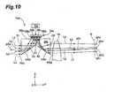
- the specific configuration and action of the spatial light modulation unit 74Awill be described below with reference to Figs. 10 and 11 . Since the spatial light modulation unit 74B basically has the same configuration as the spatial light modulation unit 74A, redundant description is omitted about the specific configuration and action of the spatial light modulation unit 74B.
- the spatial light modulation unit 74Aas shown in Fig. 10 , has a prism 23b made of an optical material, e.g., fluorite, and a reflective spatial light modulator 23a attached in proximity to a side face 23ba of the prism 23b parallel to the XY plane.
- the optical material for making the prism 23bdoes not have to be limited to fluorite, but may be silica or any other optical material according to the wavelength of the light supplied from the light source 1.
- the prism 23bhas a form obtained by replacing one side face of a rectangular parallelepiped (a side face opposed to the side face 23ba to which the spatial light modulator 23a is attached in proximity) by side faces 23bb and 23bc depressed in a V-shape, and is also called a K prism because of the sectional shape along the YZ plane.
- the side faces 23bb and 23bc depressed in the V-shape in the prism 23bare defined by two planes PN1 and PN2 intersecting at an obtuse angle.
- the two planes PN1 and PN2both are orthogonal to the YZ plane and make the V-shape along the YZ plane.
- Internal surfaces of the two side faces 23bb and 23bc in contact along an intersecting line (straight line extending in the X-direction) P3 between the two planes PN1 and PN2function as reflecting surfaces R1 and R2.
- the reflecting surface R1is located on the plane PN1
- the reflecting surface R2is located on the plane PN2
- an angle between the reflecting surfaces R1 and R2is an obtuse angle.
- the anglescan be determined as follows: the angle between the reflecting surfaces R1 and R2 is 120°; the angle between the entrance surface IP of the prism 23b perpendicular to the optical axis AXa, and the reflecting surface R1 is 60°; the angle between the exit surface OP of the prism 23b perpendicular to the optical axis AXa, and the reflecting surface R2 is 60°.
- the side face 23ba to which the spatial light modulator 23a is attached in proximityis parallel to the optical axis AXa; and the reflecting surface R1 is located on the light source 1 side (on the upstream side of the exposure apparatus; on the left in Fig. 10 ) and the reflecting surface R2 is located on the afocal lens 4 side (on the downstream side of the exposure apparatus; on the right in Fig. 10 ).
- the reflecting surface R1is obliquely arranged with respect to the optical axis AXa and the reflecting surface R2 is obliquely arranged with respect to the optical axis AXa and in symmetry with the reflecting surface R1 with respect to a plane passing the intersecting line P3 and being parallel to the XZ plane.
- the side face 23ba of the prism 23bis an optical surface opposed to a surface on which the plurality of mirror elements SE of the spatial light modulator 23a are arranged, as described below.
- the reflecting surface R1 of the prism 23breflects the light incident through the entrance surface IP, toward the spatial light modulator 23a.
- the spatial light modulator 23ais located in the optical path between the reflecting surface R1 and the reflecting surface R2 and reflects the light incident via the reflecting surface R1.
- the reflecting surface R2 of the prism 23breflects the light incident via the spatial light modulator 23a to guide the reflected light through the exit surface OP to the front lens unit 4a of the afocal lens 4.
- the optical pathsare expanded so that the optical axis AXa extends linearly on the rear side of the spatial light modulation unit 74A, for easier understanding of description.
- Fig. 10shows the example wherein the prism 23b is integrally made of one optical block, but the prism 23b may be constructed using a plurality of optical blocks.
- the spatial light modulator 23aapplies spatial modulation according to a position of incidence of light, to the light incident via the reflecting surface R1.
- the spatial light modulator 23ais provided with a plurality of micro mirror elements (optical elements) SE arranged two-dimensionally, as shown in Fig. 11 .
- Figs. 10 and 11show a configuration example in which the spatial light modulator 23a has sixteen mirror elements SE of a 4 ⁇ 4 matrix, but the spatial light modulator actually has a much larger number of mirror elements than sixteen elements.
- a ray L1is incident to a mirror element SEa out of the plurality of mirror elements SE
- a ray L2is incident to a mirror element SEb different from the mirror element SEa
- a ray L3is incident to a mirror element SEc different from the mirror elements SEa
- SEband a ray L4 is incident to a mirror element SEd different from the mirror elements SEa-SEc.
- the mirror elements SEa-SEdapply respective spatial modulations set according to their positions, to the rays L1-L4, respectively.
- the spatial light modulation unit 23is so configured that in the standard state in which the reflecting surfaces of all the mirror elements SE of the spatial light modulator 23a are set in parallel with the XY plane, the rays incident along a direction parallel to the optical axis AXa to the reflecting surface R1 travel via the spatial light modulator 23a and thereafter are reflected to a direction parallel to the optical axis AXa by the reflecting surface R2. Furthermore, the spatial light modulation unit 23 is so configured that an air-equivalent length from the entrance surface IP of the prism 23b via the mirror elements SEa-SEd to the exit surface OP is equal to an air-equivalent length from the position corresponding to the entrance surface IP to the position corresponding to the exit surface OP without the prism 23b in the optical path.
- An air-equivalent length hereinis obtained by converting an optical path length in an optical system into an optical path length in air having the refractive index of 1, and an air-equivalent length in a medium having the refractive index n is obtained by multiplying an optical path length therein by 1/n.
- the surface in which the plurality of mirror elements SE of the spatial light modulator 23a are arrayedis positioned at or near the rear focal point of the condenser lens 72 and positioned at or near the front focal point of the afocal lens 4. Therefore, a beam having a cross section of a shape according to the characteristic of the diffractive optical element 71 (e.g., a rectangular shape) is incident to the spatial light modulator 23a.
- the light reflected by the mirror elements SEa-SEd of the spatial light modulator 23a and provided with a predetermined angle distributionforms predetermined light intensity distributional areas SP1-SP4 on the pupil plane 4c of the afocal lens 4.
- the front lens unit 4a of the afocal lens 4converts angles given to the exiting light by the mirror elements SEa-SEd of the spatial light modulator 23a, into positions on the plane 4c being a far field region (Fraunhofer diffraction region) of the spatial light modulator 23a.
- the entrance surface of the cylindrical micro fly's eye lens 8is positioned at or near a position optically conjugate with the pupil plane 4c (not shown in Fig. 1 ) of the afocal lens 4. Therefore, the light intensity distribution (luminance distribution) of the secondary light source formed by the cylindrical micro fly's eye lens 8 is a distribution according to the light intensity distributional areas SP1-SP4 formed on the pupil plane 4c by the spatial light modulator 23a and the front lens unit 4a of the afocal lens 4.
- the spatial light modulator 23ais a movable multi-mirror including the mirror elements SE being a large number of micro reflecting elements arranged regularly and two-dimensionally along one plane with a reflecting surface of a planar shape up, as shown in Fig. 11 .
- Each mirror element SEis movable and an inclination of the reflecting surface thereof, i.e., an angle and direction of inclination of the reflecting surface, is independently controlled by the action of the drive unit 23c (not shown in Fig. 11 ) operating according to commands from the control unit (not shown).
- Each mirror element SEcan be continuously or discretely rotated by a desired angle of rotation around each of axes of rotation along two directions (X-direction and Y-direction) orthogonal to each other and parallel to the reflecting surface. Namely, inclinations of the reflecting surfaces of the respective mirror elements SE can be controlled two-dimensionally.
- a preferred switch controlis such that the angle of rotation is switched in multiple stages (e.g., ..., -2.5°, -2.0°, ..., 0°, +0.5°, ..., +2.5°,).
- Fig. 11shows the mirror elements SE with the contour of the square shape, but the contour of the mirror elements SE is not limited to the square.
- the contourmay be a shape permitting arrangement of the mirror elements SE with a gap as small as possible (a shape permitting closest packing), from the viewpoint of efficiency of utilization of light.
- the spacing between two adjacent mirror elements SEmay be minimum necessary, from the viewpoint of the light utilization efficiency.
- the postures of the respective mirror elements SEare changed by the action of the drive unit 23c operating according to control signals from the control unit, whereby each mirror element SE is set in a predetermined orientation.
- the rays reflected at respective predetermined angles by the mirror elements SE of the spatial light modulator 23atravel through the afocal lens 4 and zoom lens 7 to form a light intensity distribution (illumination pupil luminance distribution) of a multi-polar shape (quadrupolar, pentapolar, ...)or another shape on the rear focal point of the cylindrical micro fly's eye lens 8 or on the illumination pupil near it.
- This illumination pupil luminance distributionvaries similarly (isotropically) by the action of the zoom lens 7.
- laterally polarized light reflected at respective predetermined angles by the mirror elements SE of the spatial light modulator 23a in the spatial light modulation unit 74Aforms, for example, two circular light intensity distributional areas 41a and 41b spaced in the Z-direction with a center on the optical axis AX, on the pupil plane 4c of the afocal lens 4, as shown in Fig. 4 .
- the light forming the light intensity distributional areas 41a and 41bhas the polarization direction along the X-direction as indicated by double-headed arrows in the drawing.
- vertically polarized light reflected at respective predetermined angles by the mirror elements of the spatial light modulator in the spatial light modulation unit 74Bforms, for example, two circular light intensity distributional areas 41c and 41d spaced in the X-direction with a center on the optical axis AX, on the pupil plane 4c of the afocal lens 4, as shown in Fig. 4 .
- the light forming the light intensity distributional areas 41c and 41 dhas the polarization direction along the Z-direction as indicated by double-headed arrows in the drawing.
- the light forming the quadrupolar light intensity distribution 41 on the pupil plane 4c of the afocal lens 4forms quadrupolar light intensity distributional areas corresponding to the light intensity distributional areas 41a-41d, on the entrance surface of the cylindrical micro fly's eye lens 8, and on the rear focal plane of the cylindrical micro fly's eye lens 8 or on the illumination pupil near it (the position where the aperture stop 9 is arranged). Furthermore, quadrupolar light intensity distributional areas corresponding to the light intensity distributional areas 41 a-41 d are also formed at other illumination pupil positions optically conjugate with the aperture stop 9, i.e., at the pupil position of the imaging optical system 12 and at the pupil position of the projection optical system PL.
- the spatial light modulation unit 74Aacts, for example, to form two circular light intensity distributional areas 42a and 42b spaced in the Z-direction with a center on the optical axis AX, and a circular light intensity distributional area 42c' with a center on the optical axis AX, as shown in the left view in Fig. 5 , on the pupil plane 4c of the afocal lens 4.
- the light forming the light intensity distributional areas 42a, 42b, 42c'has the polarization direction along the X-direction as indicated by double-headed arrows in the drawing.
- the spatial light modulation unit 74Bacts, for example, to form two circular light intensity distributional areas 42d and 42e spaced in the X-direction with a center on the optical axis AX, and a circular light intensity distributional area 42c" with a center on the optical axis AX, as shown in the center view in Fig. 5 , on the pupil plane 4c of the afocal lens 4.
- the light forming the light intensity distributional areas 42d, 42e, 42c"has the polarization direction along the Z-direction as indicated by double-headed arrows in the drawing.
- the light intensity distributional areas 42a-42e of the pentapolar shapeare formed on the pupil plane 4c of the afocal lens 4, as shown in the right view in Fig. 5 .
- the circular light intensity distributional area 42c with a center on the optical axis AXis formed by superposition of the light intensity distributional areas 42c' and 42c".
- the beam with the polarization direction along the Z-direction and the beam with the polarization direction along the X-directionpass through the region of the light intensity distributional area 42c, as indicated by the double-headed arrows in the drawing.
- the modification example of Fig. 9is feasible to freely and quickly change the illumination pupil luminance distribution consisting of the first light intensity distribution in the laterally polarized state formed on the pupil plane by the action of the spatial light modulator in the spatial light modulation unit 74A and the second light intensity distribution in the vertically polarized state formed on the pupil plane by the action of the spatial light modulator in the spatial light modulation unit 74B.
- the modification example of Fig. 9is also able to realize the illumination conditions of great variety in terms of the shape, size, and polarization state of the illumination pupil luminance distribution, by changing each of the shapes and sizes of the first light intensity distribution and the second light intensity distribution in mutually different polarization states, as in the embodiment of Fig 1 .
- the modification example of Fig. 9uses the diffractive optical element 71 as a light splitter, it has the advantage that an improvement can be made in evenness of the intensity of light incident to the spatial light modulators in the spatial light modulation units 74A, 74B. Since there is no variation in angles of the beams immediately after the diffractive optical element 71 even when the position of the beam incident to the diffractive optical element 71 varies, the modification example has the advantage that the positions of the beams incident to the spatial light modulators in the spatial light modulation units 74A, 74B are unlikely to vary.
- the incident beammay be split in the shorter-side direction of the rectangular cross section, in order to miniaturize the prism 23b and, therefore, miniaturize the spatial light modulation units 74A and 74B.
- the incident beammay be split in a plane a normal to which is a longitudinal direction of effective regions of the spatial light modulators in the spatial light modulation units 74A, 74B.
- the spatial light modulation units 74A and 74Bcan be compactified by splitting the incident beam along the first direction.
- the diffractive optical element 71is used to split the incident beam into two beams.
- a prism unit 76 having a pair of prism members 76a and 76bfor example, as shown in Fig. 12 .
- the modification example of Fig. 12has the configuration similar to the modification example of Fig. 9 , but is different from the modification example of Fig. 9 only in that the prism unit 76 is arranged instead of the diffractive optical element 71 and the condenser lens 72.
- the prism unit 76 functioning as a light splitter in the modification example of Fig. 12is composed of the following members arranged in the order named from the light source side (from the left in the drawing): first prism member 76a with a plane on the light source side and with a refracting surface of a concave and V-shape on the mask side (on the right in the drawing); and second prism member 76b with a plane on the mask side and with a refracting surface of a convex and V-shape on the light source side.
- the concave refracting surface of the first prism member 76ais composed of two planes and an intersecting line (ridge line) between them extends along the X-direction.
- the convex refracting surface of the second prism member 76bis formed so as to be complementary to the concave refracting surface of the first prism member 76a.
- the convex refracting surface of the second prism member 76bis also composed of two planes and an intersecting line (ridge line) between them extends along the X-direction.
- the prism unit 76 as a light splitteris composed of the pair of prism members 76a and 76b, but it is also possible to construct the light splitter of at least one prism. Furthermore, it is possible to contemplate various forms for specific configurations of the light splitter.
- each of the half wave plates 73A and 73Bis provided in the optical path between the condenser lens 72 and the spatial light modulation units 74A and 74B.
- the half wave plates 73A and 73Bcan also be located at another appropriate position in the optical path of the first beam and at another appropriate position in the optical path of the second beam out of the two beams split by the diffractive optical element 71 or by the prism unit 76.
- the half wave plate 73A rotatable around the predetermined axisis provided in the optical path of the first beam and the half wave plate 73B rotatable around the predetermined axis is provided in the optical path of the second beam.
- a half wave plateis provided so as to be rotatable around a predetermined axis or stationary, in at least one optical path, or a configuration wherein a polarizer or an optical rotator other than the half wave plate is provided so as to be rotatable around a predetermined axis or stationary, in at least one optical path.
- the half wave plate(polarizer or optical rotator in general) may be arranged as detachable from the optical path so that it can be retracted from the optical path when not needed, which can lengthen the life of the half wave plate.
- the half wave plate(polarizer or optical rotator in general) can be arranged as replaceable with a glass substrate having the same path length, which can also lengthen the life of the half wave plate.
- elliptically polarized lightcan be controlled into desired linearly polarized light.
- a depolarizerdepolarizing element
- specklecan be reduced by about 1 / 2 .
- the illumination optical apparatususes the optical unit (spatial light modulation unit) with the pair of spatial light modulators in which the postures of the mirror elements are individually varied, it is feasible to freely and quickly change the illumination pupil luminance distribution consisting of the first light intensity distribution in the first polarization state formed on the illumination pupil by the action of the first spatial light modulator and the second light intensity distribution in the second polarization state formed on the illumination pupil by the action of the second spatial light modulator.
- the illumination pupil luminance distributionconsisting of the first light intensity distribution in the first polarization state formed on the illumination pupil by the action of the first spatial light modulator and the second light intensity distribution in the second polarization state formed on the illumination pupil by the action of the second spatial light modulator.
- the illumination optical apparatusis able to realize the illumination conditions of great variety in terms of the shape, the size, and the polarization state of the illumination pupil luminance distribution. Furthermore, the exposure apparatus according to the embodiment and modification examples is able to perform good exposure under an appropriate illumination condition realized according to a pattern characteristic of a mask M, using the illumination optical apparatus capable of realizing the illumination conditions of great variety, and, therefore, to manufacture good devices.
- the apparatusmay also be configured as follows: a pupil luminance distribution measuring device is used to measure the illumination pupil luminance distribution during formation of the illumination pupil luminance distribution by means of the spatial light modulation unit and each spatial light modulator in the spatial light modulation unit is controlled according to the result of the measurement.
- a pupil luminance distribution measuring deviceis used to measure the illumination pupil luminance distribution during formation of the illumination pupil luminance distribution by means of the spatial light modulation unit and each spatial light modulator in the spatial light modulation unit is controlled according to the result of the measurement.
- the maskcan be replaced by a variable pattern forming device which forms a predetermined pattern on the basis of predetermined electronic data.
- the use of this variable pattern forming deviceminimizes the effect on synchronization accuracy even when the pattern surface is vertical.
- the variable pattern forming device applicable hereincan be, for example, a DMD (Digital Micromirror Device) including a plurality of reflecting elements driven based on predetermined electronic data.
- the exposure apparatus using DMDis disclosed, for example, in Japanese Patent Application Laid-open No. 2004-304135 and International Publication WO2006/080285 and U.S Pat. Published Application No. 2007/0296936 corresponding thereto.
- the reflective spatial light modulators of the non-emission type like DMDit is also possible to use transmissive spatial light modulators or to use self-emission type image display devices.
- the variable pattern forming devicemay also be used in cases where the pattern surface is horizontal.
- the exposure apparatusis manufactured by assembling various sub-systems containing their respective components as set forth in the scope of claims in the present application, so as to maintain predetermined mechanical accuracy, electrical accuracy, and optical accuracy.
- the following adjustmentsare carried out before and after the assembling: adjustment for achieving the optical accuracy for various optical systems; adjustment for achieving the mechanical accuracy for various mechanical systems; adjustment for achieving the electrical accuracy for various electrical systems.
- the assembling steps from the various sub-systems into the exposure apparatusinclude mechanical connections, wire connections of electric circuits, pipe connections of pneumatic circuits, etc. between the various sub-systems.
- Fig. 13is a flowchart showing manufacturing steps of semiconductor devices.
- the manufacturing steps of semiconductor devicesinclude depositing a metal film on a wafer W to become a substrate for semiconductor devices (step S40); and applying a photoresist as a photosensitive substrate onto the deposited metal film (step S42).
- the subsequent stepsinclude transferring a pattern formed on a mask (reticle) M, into each shot area on the wafer W, using the projection exposure apparatus of the above embodiment (step S44: exposure step); and performing development of the wafer W after completion of the transfer, i.e., development of the photoresist onto which the pattern has been transferred (step S46: development step).
- a step subsequent theretois to process the surface of the wafer W by etching or the like, using the resist pattern made on the surface of the wafer W in step S46, as a mask (step S48: processing step).
- the resist pattern hereinis a photoresist layer in which projections and depressions are formed in the shape corresponding to the pattern transferred by the projection exposure apparatus of the above embodiment, and which the depressions penetrate throughout.
- the surface of the wafer Wis processed through this resist pattern.
- the processing carried out in the step S48includes, for example, at least either etching of the surface of the wafer W or deposition of a metal film or the like.
- the projection exposure apparatus of the above embodimentperforms the transfer of the pattern using the wafer W coated with the photoresist, as a photosensitive substrate or plate P.
- Fig. 14is a flowchart showing manufacturing steps of a liquid crystal device such as a liquid-crystal display device. As shown in Fig. 14 , manufacturing steps of the liquid crystal device include sequentially carrying out a pattern forming step (step S50), a color filter forming step (step S52), a cell assembly step (step S54), and a module assembly step (step S56).
- the pattern forming step of step S50is to form a predetermined pattern such as a circuit pattern and an electrode pattern on a glass substrate coated with a photoresist, as a plate P, using the projection exposure apparatus of the above embodiment.
- This pattern forming stepincludes an exposure step of transferring a pattern onto a photoresist layer by means of the projection exposure apparatus of the above embodiment; a development step of developing the plate P after the transfer of the pattern, i.e., developing the photoresist layer on the glass substrate, to make the photoresist layer in the shape corresponding to the pattern; and a processing step of processing the surface of the glass substrate through the developed photoresist layer.
- the color filter forming step of step S52is to form a color filter in a configuration wherein a large number of sets of three dots corresponding to R (Red), G (Green), and B (Blue) are arrayed in a matrix pattern, or in a configuration wherein a plurality of sets of three stripe filters of R, G, and B are arrayed in a horizontal scan direction.
- the cell assembly step of step S54is to assemble a liquid crystal panel (liquid crystal cell) using the glass substrate with the predetermined pattern thereon in step S50 and the color filter formed in step S52. Specifically, the liquid crystal panel is formed, for example, by pouring a liquid crystal into between the glass substrate and the color filter.
- the module assembly step of step S56is to attach various components such as electric circuits and backlights for display operation of this liquid crystal panel, to the liquid crystal panel assembled in step S54.
- the present inventionis not limited to the application to the exposure apparatus for manufacture of semiconductor devices, but can also be widely applied, for example, to the exposure apparatus for display devices such as liquid-crystal display devices formed with rectangular glass plates, or plasma displays and to the exposure apparatus for manufacture of various devices such as imaging devices (CCDs or the like), micromachines, thin-film magnetic heads, and DNA chips. Furthermore, the present invention can also be applied to the exposure step (exposure apparatus) in manufacture of masks (photomasks, reticles, etc.) with mask patterns of various devices by photolithography.
- the aforementioned embodimentused the ArF excimer laser light (the wavelength: 193 nm) or the KrF excimer laser light (the wavelength: 248 nm) as the exposure light, but the exposure light does not have to be limited to these: the present invention can also be applied to any other appropriate laser light source, e.g., an F 2 laser light source which supplies the laser light at the wavelength of 157 nm.
- an F 2 laser light sourcewhich supplies the laser light at the wavelength of 157 nm.
- a technique of filling the interior of the optical path between the projection optical system and the photosensitive substrate with a medium having the refractive index larger than 1.1typically, a liquid
- a liquid immersion methodit is possible to adopt one of the following techniques as a technique of filling the interior of the optical path between the projection optical system and the photosensitive substrate with the liquid: the technique of locally filling the optical path with the liquid as disclosed in International Publication WO99/49504 ; the technique of moving a stage holding the substrate to be exposed, in a liquid bath as disclosed in Japanese Patent Application Laid-open No.
Landscapes
- Physics & Mathematics (AREA)
- General Physics & Mathematics (AREA)
- Optics & Photonics (AREA)
- Engineering & Computer Science (AREA)
- General Engineering & Computer Science (AREA)
- Chemical & Material Sciences (AREA)
- Crystallography & Structural Chemistry (AREA)
- Spectroscopy & Molecular Physics (AREA)
- Exposure And Positioning Against Photoresist Photosensitive Materials (AREA)
- Exposure Of Semiconductors, Excluding Electron Or Ion Beam Exposure (AREA)
- Microscoopes, Condenser (AREA)
- Optical Elements Other Than Lenses (AREA)
Abstract
Description
- The present invention relates to an optical unit, an illumination optical apparatus, an exposure apparatus, and a device manufacturing method. More particularly, the present invention relates to an illumination optical apparatus suitably applicable to an exposure apparatus for manufacturing such devices as semiconductor devices, imaging devices, liquid-crystal display devices, and thin-film magnetic heads by lithography.
- In a typical exposure apparatus of this type, a light beam emitted from a light source travels through a fly's eye lens as an optical integrator to form a secondary light source (a predetermined light intensity distribution on an illumination pupil in general) as a substantial surface illuminant consisting of a large number of light sources. The light intensity distribution on the illumination pupil will be referred to hereinafter as "illumination pupil luminance distribution." The illumination pupil is defined as a position such that an illumination target surface becomes a Fourier transform surface of the illumination pupil by action of an optical system between the illumination pupil and the illumination target surface (a mask or a wafer in the case of the exposure apparatus).
- Beams from the secondary light source are condensed by a condenser lens to superposedly illuminate the mask on which a predetermined pattern is formed. Light passing through the mask travels through a projection optical system to be focused on the wafer, whereby the mask pattern is projected (or transferred) onto the wafer to effect exposure thereof. Since the pattern formed on the mask is a highly integrated one, an even illuminance distribution must be obtained on the wafer in order to accurately transfer this fine pattern onto the wafer.
- There is a conventionally proposed illumination optical apparatus capable of continuously changing the illumination pupil luminance distribution (and, therefore, the illumination condition) without use of a zoom optical system (cf. Japanese Patent Application Laid-open No.
2002-353105 - An object of the present invention is to provide an illumination optical apparatus capable of realizing illumination conditions of greater variety in terms of the shape and size of the illumination pupil luminance distribution. Another object of the present invention is to provide an exposure apparatus capable of performing good exposure under an appropriate illumination condition realized according to a pattern characteristic, using the illumination optical apparatus capable of realizing the illumination conditions of great variety.
- In order to achieve the above object, a first aspect of the present invention provides an optical unit comprising:
- a light splitter to split an incident beam traveling in an incident light path, into a plurality of beams;
- a first spatial light modulator which can be arranged in an optical path of a first beam out of the plurality of beams;
- a second spatial light modulator which can be arranged in an optical path of a second beam out of the plurality of beams; and
- a light combiner to combine a beam having passed via the first spatial light modulator, with a beam having passed via the second spatial light modulator, and to direct a resultant beam to an exiting light path;
- A second aspect of the present invention provides an illumination optical apparatus to illuminate an illumination target surface on the basis of light from a light source, the illumination optical apparatus comprising:
- the optical unit of the first aspect; and
- a distribution forming optical system which forms a predetermined light intensity distribution on an illumination pupil of the illumination optical apparatus, based on the beams having passed via the first and second spatial light modulators.
- A third aspect of the present invention provides an exposure apparatus comprising the illumination optical apparatus of the second aspect for illuminating a predetermined pattern, the exposure apparatus performing exposure of the predetermined pattern on a photosensitive substrate.
- A fourth aspect of the present invention provides a device manufacturing method comprising:
- an exposure step of effecting the exposure of the predetermined pattern on the photosensitive substrate, using the exposure apparatus of the third aspect;
- a development step of developing the photosensitive substrate onto which the pattern has been transferred, to form a mask layer in a shape corresponding to the pattern on a surface of the photosensitive substrate; and
- a processing step of processing the surface of the photosensitive substrate through the mask layer.
- The illumination optical apparatus of the present invention is able to realize the illumination conditions of greater variety in terms of the shape and the size of the illumination pupil luminance distribution. The exposure apparatus of the present invention is able to perform good exposure under an appropriate illumination condition realized according to a pattern characteristic of a mask M, using the illumination optical apparatus capable of realizing the illumination conditions of great variety, and, therefore, to manufacture good devices.
Fig. 1 is a drawing schematically showing a configuration of an exposure apparatus according to an embodiment of the present invention.Fig. 2 is a drawing schematically showing a configuration of a spatial light modulation unit.Fig. 3 is a perspective view schematically showing a configuration of a cylindrical micro fly's eye lens.Fig. 4 is a drawing schematically showing a light intensity distribution of a quadrupolar shape formed on a pupil plane of an afocal lens in the embodiment.Fig. 5 is a drawing schematically showing an example of forming an illumination pupil luminance distribution of a pentapolar shape in the embodiment.Fig. 6 is a drawing schematically showing a configuration of a spatial light modulation unit according to a modification example in which a light splitter and a light combiner include a common polarization beam splitter.Fig. 7 is a drawing schematically showing a configuration of a spatial light modulation unit according to another modification example having transmissive spatial light modulators.Fig. 8 is a drawing schematically showing a configuration of an exposure apparatus according to a modification example having a polarization control unit.Fig. 9 is a drawing schematically showing a major configuration of a modification example using a diffractive optical element as a light splitter.Fig. 10 is a drawing schematically showing a configuration of the spatial light modulation unit shown inFig. 9 .Fig. 11 a partial perspective view of a spatial light modulator in the spatial light modulation unit shown inFig. 9 .Fig. 12 is a drawing schematically showing a major configuration of a modification example using a prism unit as a light splitter.Fig. 13 is a flowchart showing manufacturing steps of semiconductor devices.Fig. 14 is a flowchart showing manufacturing steps of a liquid crystal device such as a liquid-crystal display device.- Embodiments of the present invention will be described on the basis of the accompanying drawings.
Fig. 1 is a drawing schematically showing a configuration of an exposure apparatus according to an embodiment of the present invention.Fig. 2 is a drawing schematically showing a configuration of a spatial light modulation unit. InFig. 1 , the Z-axis is set along a direction of a normal to a wafer W being a photosensitive substrate, the Y-axis along a direction parallel to the plane ofFig. 1 in a surface of the wafer W, and the X-axis along a direction perpendicular to the plane ofFig. 1 in the surface of the wafer W. - With reference to
Fig. 1 , the exposure apparatus of the present embodiment is provided with alight source 1 for supplying exposure light (illumination light). Thelight source 1 can be, for example, an ArF excimer laser light source which supplies light at the wavelength of 193 nm, or a KrF excimer laser light source which supplies light at the wavelength of 248 nm. Light emitted from thelight source 1 is expanded into a beam of a required sectional shape by a shapingoptical system 2 and then the expanded beam is incident to a spatiallight modulation unit 3. - The spatial
light modulation unit 3, as shown inFig. 2 , has a pair ofprism members spatial light modulators entrance face 31a of theprism member 31 in the spatiallight modulation unit 3 propagates inside theprism member 31 and thereafter impinges upon apolarization separating film 35 formed between theprism members polarization separating film 35 propagates inside theprism member 31 and thereafter impinges upon the firstspatial light modulator 33. - The first
spatial light modulator 33 has a plurality of mirror elements (optical elements in general) 33a arranged two-dimensionally, and adrive unit 33b (not shown inFig. 1 ) which individually controls and drives postures of themirror elements 33a. Similarly, the secondspatial light modulator 34 has a plurality ofmirror elements 34a arranged two-dimensionally, and adrive unit 34b (not shown inFig. 1 ) which individually controls and drives postures of themirror elements 34a. Thedrive units mirror elements - Light reflected by the
mirror elements 33a of the firstspatial light modulator 33 propagates inside theprism member 31 and thereafter is incident in the s-polarized state to apolarization separating film 36 formed between theprism members spatial light modulator 33 to be reflected on thepolarization separating film 36, propagates inside theprism member 31 and is then emitted from anexit face 31 b of theprism member 31 to the outside of the spatiallight modulation unit 3. In a standard state in which reflecting surfaces of all themirror elements 33a in the firstspatial light modulator 33 are positioned along the XY plane, the light having traveled along the optical axis AX into the spatiallight modulation unit 3 and then via the firstspatial light modulator 33 is emitted along the optical axis AX from the spatiallight modulation unit 3. - On the other hand, p-polarized light having passed through the
polarization separating film 35 propagates inside theprism member 32 and is totally reflected on aninterface 32a between theprism member 32 and a gas (air or inert gas) 37. Thereafter, the totally reflected light is incident to the second spatiallight modulator 34. Light reflected by themirror elements 34a in the second spatiallight modulator 34 propagates inside theprism member 32 and is totally reflected on aninterface 32b between theprism member 32 and thegas 37. Thereafter, the totally reflected light is incident in the p-polarized state to thepolarization separating film 36 formed between theprism members - The light having traveled via the second spatial
light modulator 34 and having been transmitted by thepolarization separating film 36, propagates inside theprism member 31 and then is emitted from theexit face 31b of theprism member 31 to the outside of the spatiallight modulation unit 3. In a standard state in which reflecting surfaces of all themirror elements 34a in the second spatiallight modulator 34 are positioned along the XY plane, the light having traveled along the optical axis AX into the spatiallight modulation unit 3 and then via the second spatiallight modulator 34, is emitted along the optical axis AX from the spatiallight modulation unit 3. - In the spatial
light modulation unit 3, as described above, thepolarization separating film 35 formed between theprism members polarization separating film 36 formed between theprism members light modulator 33, with the beam having traveled via the second spatiallight modulator 34. - The light emitted from the spatial
light modulation unit 3 is then incident to anafocal lens 4. Theafocal lens 4 is an afocal system (afocal optic) that is so set that the front focal point thereof is approximately coincident with the position of themirror elements 33a of the first spatiallight modulator 33 and with the position of themirror elements 34a of the second spatiallight modulator 34 and that the rear focal point thereof is approximately coincident with a position of apredetermined plane 5 indicated by a dashed line in the drawing. - Therefore, the s-polarized beam having traveled via the first spatial
light modulator 33 forms, for example, a light intensity distribution of a Z-directionally dipolar shape consisting of two circular light intensity distributional areas spaced in the Z-direction with a center on the optical axis AX, on the pupil plane of theafocal lens 4, and thereafter is emitted in the dipolar angle distribution from theafocal lens 4. On the other hand, the p-polarized beam having traveled via the second spatiallight modulator 34 forms, for example, a light intensity distribution of an X-directionally dipolar shape consisting of two circular light intensity distributional areas spaced in the X-direction with a center on the optical axis AX, on the pupil plane of theafocal lens 4, and thereafter is emitted in the dipolar angle distribution from theafocal lens 4. - A
conical axicon system 6 is arranged at the position of the pupil plane of theafocal lens 4 or at a position near it in the optical path between afront lens unit 4a and arear lens unit 4b of theafocal lens 4. The configuration and action of theconical axicon system 6 will be described later. The beam having passed through theafocal lens 4 travels through azoom lens 7 for variation in σ value (σ value = mask-side numerical aperture of the illumination optical apparatus/mask-side numerical aperture of the projection optical system) and then enters a cylindrical micro fly'seye lens 8. - The cylindrical micro fly's
eye lens 8, as shown inFig. 3 , is composed of a first fly'seye member 8a arranged on the light source side and a second fly'seye member 8b arranged on the mask side. Cylindrical lens groups 8aa and 8ba arrayed in the X-direction are formed each at the pitch p1 in the light-source-side surface of the first fly'seye member 8a and in the light-source-side surface of the second fly'seye member 8b, respectively. Cylindrical lens groups 8ab and 8bb arrayed in the Z-direction are formed each at the pitch p2 (p2 > p1) in the mask-side surface of the first fly'seye member 8a and in the mask-side surface of the second fly'seye member 8b, respectively. - When attention is focused on the refracting action in the X-direction of the cylindrical micro fly's eye lens 8 (i.e., the refracting action in the XY plane), the wavefront of a parallel beam incident along the optical axis AX is divided at the pitch p1 along the X-direction by the cylindrical lens group 8aa formed on the light source side of the first fly's
eye member 8a, the divided beams are condensed by refracting faces of the cylindrical lens group, the condensed beams are then condensed by refracting faces of the corresponding cylindrical lenses in the cylindrical lens group 8ba formed on the light source side of the second fly'seye member 8b, and the condensed beams are converged on the rear focal plane of the cylindrical micro fly'seye lens 8. - When attention is focused on the refracting action in the Z-direction of the cylindrical micro fly's eye lens 8 (i.e., the refracting action in the YZ plane), the wavefront of a parallel beam incident along the optical axis AX is divided at the pitch p2 along the Z-direction by the cylindrical lens group 8ab formed on the mask side of the first fly's
eye member 8a, the divided beams are condensed by refracting faces of the cylindrical lens group, the condensed beams are then condensed by refracting faces of the corresponding cylindrical lenses in the cylindrical lens group 8bb formed on the mask side of the second fly'seye member 8b, and the condensed beams are converged on the rear focal plane of the cylindrical micro fly'seye lens 8. - As described above, the cylindrical micro fly's
eye lens 8 is composed of the first fly'seye member 8a and the second fly'seye member 8b in each of which the cylindrical lens groups are arranged on the two side faces thereof, and exercises the same optical function as a micro fly's eye lens in which a large number of micro refracting faces of a rectangular shape in the size of p1 in the X-direction and in the size of p2 in the Z-direction are integrally formed horizontally and vertically and densely. The cylindrical micro fly'seye lens 8 is able to achieve smaller change in distortion due to variation in surface shapes of the micro refracting faces and, for example, to keep less influence on the illuminance distribution from manufacture errors of the large number of micro refracting faces integrally formed by etching. - The position of the
predetermined plane 5 is located near the front focal point of thezoom lens 7 and the entrance surface of the cylindrical micro fly'seye lens 8 is located near the rear focal point of thezoom lens 7. In other words, thezoom lens 7 sets thepredetermined plane 5 and the entrance surface of the cylindrical micro fly'seye lens 8 substantially in the Fourier transform relation and, thus, keeps the pupil plane of theafocal lens 4 approximately optically conjugate with the entrance surface of the cylindrical micro fly'seye lens 8. - Therefore, for example, a quadrupolar illumination field consisting of two circular light intensity distributional areas spaced in the Z-direction with a center on the optical axis AX and two circular light intensity distributional areas spaced in the X-direction with a center on the optical axis AX is formed on the entrance surface of the cylindrical micro fly's
eye lens 8 as on the pupil plane of theafocal lens 4. The overall shape of this quadrupolar illumination field similarly varies depending upon the focal length of thezoom lens 7. The rectangular micro refracting faces as wavefront division units in the cylindrical micro fly'seye lens 8 are of a rectangular shape similar to a shape of an illumination field to be formed on the mask M (and, therefore, similar to a shape of an exposure region to be formed on the wafer W). - The beam incident to the cylindrical micro fly's
eye lens 8 is two-dimensionally divided to form a secondary light source with a light intensity distribution approximately identical with the illumination field formed by the incident beam, i.e., a secondary light source of a quadrupolar shape (quadrupolar illumination pupil luminance distribution) consisting of two circular substantial surface illuminants spaced in the Z-direction with a center on the optical axis AX and two circular substantial surface illuminants spaced in the X-direction with a center on the optical axis AX, on or near its rear focal plane (and thus on the illumination pupil). Beams from the secondary light source formed on or near the rear focal plane of the cylindrical micro fly'seye lens 8 are then incident to an aperture stop 9 located near it. - The aperture stop 9 has quadrupolar apertures (light transmitting portions) corresponding to the secondary light source of the quadrupolar shape formed on or near the rear focal plane of the cylindrical micro fly's
eye lens 8. The aperture stop 9 is configured so as to be detachable with respect to the illumination optical path and to be switchable with a plurality of aperture stops having apertures of different sizes and shapes. A method of switching the aperture stops can be, for example, a known turret method or slide method. The aperture stop 9 is arranged at a position approximately optically conjugate with an entrance pupil plane of projection optical system PL described later, and defines a range of the secondary light source that contributes to illumination. - The beams from the secondary light source limited by the aperture stop 9 travel through a condenser
optical system 10 to superposedly illuminate amask blind 11. In this way, an illumination field of a rectangular shape according to the shape and focal length of the rectangular micro refracting faces as wavefront division units of the cylindrical micro fly'seye lens 8 is formed on themask blind 11 as an illumination field stop. Beams having passed through a rectangular aperture (light transmitting portion) of themask blind 11 is condensed by an imagingoptical system 12 to superposedly illuminate a mask M on which a predetermined pattern is formed. Namely, the imagingoptical system 12 forms an image of the rectangular aperture of themask blind 11 on the mask M. - A beam having passed through the mask M held on a mask stage MS travels through the projection optical system PL to form an image of the mask pattern on a wafer (photosensitive substrate) W held on a wafer stage WS. In this manner, the pattern of the mask M is sequentially transferred into each of exposure regions on the wafer W by performing one-shot exposure or scan exposure while two-dimensionally driving and controlling the wafer stage WS in the plane (XY plane) perpendicular to the optical axis AX of the projection optical system PL and, therefore, while two-dimensionally driving and controlling the wafer W.
- The
conical axicon system 6 is composed of the following members arranged in the order named from the light source side:first prism member 6a with a plane on the light source side and with a refracting surface of a concave conical shape on the mask side; andsecond prism member 6b with a plane on the mask side and with a refracting surface of a convex conical shape on the light source side. The concave conical refracting surface of thefirst prism member 6a and the convex conical refracting surface of thesecond prism member 6b are complementarily formed so as to be able to contact each other. At least one member out of thefirst prism member 6a and thesecond prism member 6b is configured to be movable along the optical axis AX, whereby the spacing is made variable between the concave conical refracting surface of thefirst prism member 6a and the convex conical refracting surface of thesecond prism member 6b. For easier understanding, the action of theconical axicon system 6 and the action of thezoom lens 7 will be described with focus on the secondary light source of the quadrupolar or annular shape. - In a state in which the concave conical refracting surface of the
first prism member 6a and the convex conical refracting surface of thesecond prism member 6b contact each other, theconical axicon system 6 functions as a plane-parallel plate and causes no effect on the secondary light source of the quadrupolar or annular shape formed. However, as the concave conical refracting surface of thefirst prism member 6a and the convex conical refracting surface of thesecond prism member 6b are separated away from each other, the outside diameter (inside diameter) of the quadrupolar or annular secondary light source varies while keeping constant the width of the quadrupolar or annular secondary light source (half of a difference between a diameter (outside diameter) of a circle circumscribed to the quadrupolar secondary light source and a diameter (inside diameter) of a circle inscribed therein; half of a difference between the outside diameter and the inside diameter of the annular secondary light source). Namely, the annular ratio (inside diameter/outside diameter) and the size (outside diameter) of the quadrupolar or annular secondary light source vary. - The
zoom lens 7 has a function to enlarge or reduce the overall shape of the quadrupolar or annular secondary light source similarly (or isotropically). For example, as the focal length of thezoom lens 7 is increased from a minimum value to a predetermined value, the overall shape of the quadrupolar or annular secondary light source is similarly enlarged. In other words, the width and size (outside diameter) of the secondary light source both vary, without change in the annular ratio of the quadrupolar or annular secondary light source, by the action of thezoom lens 7. In this manner, the annular ratio and size (outside diameter) of the quadrupolar or annular secondary light source can be controlled by the actions of theconical axicon system 6 and thezoom lens 7. - In the present embodiment, the spatial
light modulators mirror elements 10-503300 EP 779530 2004-78136 U.S. Pat. No. 6,900,915 corresponding thereto, Japanese Patent Application Laid-open (Translation of PCT Application) No.2006-524349 U.S. Pat. No. 7,095,546 corresponding thereto, and Japanese Patent Application Laid-open No.2006-113437 mirror elements - In the first spatial
light modulator 33, each of the postures of themirror elements 33a varies by the action of thedrive unit 33b operating according to a control signal from the control unit, whereby eachmirror element 33a is set in a predetermined orientation. The s-polarized light reflected at respective predetermined angles by themirror elements 33a of the first spatiallight modulator 33 forms, for example, two circular lightintensity distributional areas afocal lens 4, as shown inFig. 4 . The light forming the lightintensity distributional areas - Similarly, in the second spatial
light modulator 34, each of the postures of themirror elements 34a varies by the action of thedrive unit 34b operating according to a control signal from the control unit, whereby eachmirror element 34a is set in a predetermined orientation. The p-polarized light reflected at respective predetermined angles by themirror elements 34a of the second spatiallight modulator 34 forms, for example, two circular lightintensity distributional areas 4 1 c and 41d spaced in the X-direction with a center on the optical axis AX, on the pupil plane of theafocal lens 4, as shown inFig. 4 . The light forming the light intensitydistributional areas light modulation unit 3 is circular polarization or linear polarization with the polarization direction at an angle of 45° to the X-axis and Z-axis (which will be referred to hereinafter as "45° linear polarization"), the light intensities of the four light intensitydistributional areas 41 a-41 d become equal to each other. - The light forming the quadrupolar
light intensity distribution 41 on the pupil plane of theafocal lens 4 forms the light intensity distribution of the quadrupolar shape corresponding to the light intensitydistributional areas 41 a-41 d on the entrance surface of the cylindrical micro fly'seye lens 8, and on the rear focal plane of the cylindrical micro fly'seye lens 8 or on the illumination pupil near it (the position where the aperture stop 9 is arranged). Namely, theafocal lens 4,zoom lens 7, and cylindrical micro fly'seye lens 8 constitute a distribution forming optical system which forms a predetermined light intensity distribution on the illumination pupil of the illumination optical apparatus (2-12), based on the beams having traveled via the first spatiallight modulator 33 and the second spatiallight modulator 34. Furthermore, the light intensity distribution of the quadrupolar shape corresponding to the lightintensity distributional areas 41a-41d is also formed at other illumination pupil positions optically conjugate with the aperture stop 9, i.e., at the pupil position of the imagingoptical system 12 and at the pupil position of the projection optical system PL. - The exposure apparatus performs exposure under an appropriate illumination condition according to a pattern characteristic, in order to highly accurately and faithfully transfer the pattern of the mask M onto the wafer W. In the present embodiment, the illumination pupil luminance distribution to be formed is the quadrupolar illumination pupil luminance distribution corresponding to the quadrupolar
light intensity distribution 41 shown inFig. 4 and the beams passing through this quadrupolar illumination pupil luminance distribution are set in a circumferential polarization state. In the circumferential polarization quadrupolar illumination based on the quadrupolar illumination pupil luminance distribution in the circumferential polarization state, the light impinging upon the wafer W as a final illumination target surface is in a polarization state in which the principal component is s-polarized light. - Here the s-polarized light is linearly polarized light with the polarization direction along a direction normal to a plane of incidence (which is polarized light with the electric vector vibrating in the direction normal to the plane of incidence). The plane of incidence is defined as a plane that includes a point where light impinges upon a boundary surface of a medium (illumination target surface: surface of wafer W) and that includes a normal to the boundary surface at that point and a direction of incidence of the light. As a consequence, the circumferential polarization quadrupolar illumination achieves an improvement in optical performance of the projection optical system (the depth of focus and others), whereby a good mask pattern image is obtained with high contrast on the wafer (photosensitive substrate).
- Since the present embodiment uses the spatial
light modulation unit 3 with the pair of spatiallight modulators mirror elements light modulator 33 and the second light intensity distribution in the p-polarized state formed on the illumination pupil by the action of the second spatiallight modulator 34. In other words, the present embodiment is able to realize the illumination conditions of great variety in terms of the shape, size, and polarization state of the illumination pupil luminance distribution, by changing each of the shapes and sizes of the first light intensity distribution and the second light intensity distribution in mutually different polarization states. - As described above, the illumination optical apparatus (2-12) to illuminate the mask M as an illumination target surface on the basis of the light from the
light source 1 in the present embodiment is able to realize the illumination conditions of great variety in terms of the shape, size, and polarization state of the illumination pupil luminance distribution. Furthermore, the exposure apparatus (1-WS) of the present embodiment is able to perform good exposure under an appropriate illumination condition realized according to the pattern characteristic of the mask M, using the illumination optical apparatus (2-12) capable of realizing the illumination conditions of great variety. - In the present embodiment, when the spatial
light modulators polarization separating film 35 functioning as a light splitter is parallel to (or coincident with) the traveling direction of the exiting beam from thepolarization separating film 36 functioning as a light combiner. In other words, in the standard state of the spatiallight modulators light modulation unit 3 and the exiting beam from the spatiallight modulation unit 3 are coincident with (or parallel to) the optical axis AX of the illumination optical apparatus. Since the optical paths upstream and downstream of the spatiallight modulation unit 3 are coaxial (or parallel), the optical system can be shared, for example, with the conventional illumination optical apparatus using a diffractive optical element for formation of the illumination pupil luminance distribution. - In the present embodiment, the
mirror elements 33a of the first spatiallight modulator 33 are arranged near theprism member 31 and themirror elements 34a of the second spatiallight modulator 34 are arranged near theprism member 32. In this case, theprism members mirror elements light modulators - In the present embodiment, the spatial
light modulation unit 3 may be so designed that the angle θ of incidence of the light (cf.Fig. 2 ) to thepolarization separating film 35 formed between theprism members polarization separating film 35 and increase polarization efficiency. Thepolarization separating films 2005-77819 U.S. Pat. No. 7,116,478 corresponding thereto. - In the above-described embodiment, the spatial
light modulation unit 3 is composed of the pair ofprism members light modulators light modulation unit 3. - In the foregoing embodiment, the
afocal lens 4,conical axicon system 6, andzoom lens 7 are arranged in the optical path between the spatiallight modulation unit 3 and the cylindrical micro fly'seye lens 8. However, without having to be limited to this, these optical members can be replaced, for example, by a condensing optical system functioning as a Fourier transform lens. - In the foregoing embodiment, the p-polarized light having traveled via the
polarization separating film 35 functioning as a light splitter is folded toward the second spatiallight modulator 34 by total reflection on theinterface 32a between theprism member 32 and thegas 37 as a first folding surface. Likewise, the p-polarized light having traveled via the second spatiallight modulator 34 is folded toward thepolarization separating film 36 functioning as a light combiner, by total reflection on theinterface 32b between theprism member 32 and thegas 37. However, without having to be limited to this, it is also possible to provide a reflecting film on theinterfaces - In the above description, the quadrupolar illumination pupil luminance distribution is formed by forming the Z-directionally dipolar light
intensity distributional areas light modulator 33 and forming the X-directionally dipolar light intensitydistributional areas light modulator 34. However, in the present embodiment, as described above, various forms can be contemplated as to the shape, size, and polarization state of the illumination pupil luminance distribution. The following will schematically describe an example of forming a pentapolar illumination pupil luminance distribution, with reference toFig. 5 . - In this example, as shown in the left view in
Fig. 5 , for example, two circular lightintensity distributional areas intensity distributional area 42c' with a center on the optical axis AX are formed on the pupil plane of theafocal lens 4 by the action of the first spatiallight modulator 33. The light forming the lightintensity distributional areas Fig. 5 , for example, two circular lightintensity distributional areas intensity distributional area 42c" with a center on the optical axis AX are formed on the pupil plane of theafocal lens 4 by the action of the second spatiallight modulator 34. The light forming the lightintensity distributional areas - As a result, the light
intensity distributional areas 42a-42e of the pentapolar shape are formed, as shown in the right view inFig. 5 , on the pupil plane of theafocal lens 4. The circular lightintensity distributional area 42c with a center on the optical axis AX is formed by superposition of the light intensitydistributional areas 42c' and 42c". When an optical path length difference of not less than a temporal coherence length of thelight source 1 is provided between the s-polarized light traveling via the first spatiallight modulator 33 to the pupil plane of theafocal lens 4 and the p-polarized light traveling via the second spatiallight modulator 34 to the pupil plane of theafocal lens 4, the beam with the polarization direction along the Z-direction and the beam with the polarization direction along the X-direction as indicated by the double-headed arrows in the drawing pass through the region of the lightintensity distributional area 42c. - In contrast to it, when there is no path length difference between the s-polarized light traveling via the first spatial
light modulator 33 to the pupil plane of theafocal lens 4 and the p-polarized light traveling via the second spatiallight modulator 34 to the pupil plane of theafocal lens 4, the polarization state of the beam passing through the region of the lightintensity distributional area 42c coincides with the polarization state of the incident beam to the spatiallight modulation unit 3. When the polarization state of the beam incident to the spatiallight modulation unit 3 is circular polarization or 45° linear polarization, the light intensities of the four surrounding lightintensity distributional areas intensity distributional area 42c is twice the light intensities of the other areas. - As another example, light having passed through a half wave plate may be made incident to the
polarization separating film 35 functioning as a light splitter. A ratio of intensities of the s-polarized light and the p-polarized light separated by thepolarization separating film 35 can be controlled by rotating the half wave plate arranged on the light source side with respect to thepolarization separating film 35, around the optical axis. Namely, it is feasible to control the ratio of intensities of s-polarized light and p-polarized light reaching the pupil plane of theafocal lens 4. It is also possible to make only the s-polarized light or p-polarized light reach the pupil plane of theafocal lens 4, for example, by controlling the angle of rotation of the half wave plate so as to make the s-polarized light incident to thepolarization separating film 35 or by controlling the angle of rotation of the half wave plate so as to make the p-polarized light incident to thepolarization separating film 35. This permits a dipolar light intensity distribution (e.g., lightintensity distributional areas Fig. 4 ) to be formed on the pupil plane of theafocal lens 4. - In the foregoing embodiment, the
polarization separating film 35 located on the light splitting surface functions as a light splitter and thepolarization separating film 36 located on the light combining surface at the position different from that of thepolarization separating film 35 functions as a light combiner. However, without having to be limited to this, it is also possible to adopt a modification example in which the light splitter and the light combiner have a commonpolarization beam splitter 51, for example, as shown inFig. 6 . In the spatiallight modulation unit 3A shown in the modification example ofFig. 6 , the s-polarized light reflected on apolarization separating film 51a, in the light incident along the optical axis AX into thepolarization beam splitter 51, travels through aquarter wave plate 52 to become circularly polarized light, and the circularly polarized light is incident to the first spatiallight modulator 53. - Light reflected by a plurality of mirror elements of the first spatial
light modulator 53 travels through thequarter wave plate 52 to become p-polarized light and the p-polarized light returns to thepolarization beam splitter 51. The p-polarized light having traveled via the first spatiallight modulator 53 to enter thepolarization beam splitter 51, passes through thepolarization separating film 51a to be emitted from thepolarization beam splitter 51. In the standard state of the first spatiallight modulator 53, the light having traveled along the optical axis AX into the spatiallight modulation unit 3A and then via the first spatiallight modulator 53 is emitted along the optical axis AX from the spatiallight modulation unit 3A. - On the other hand, the p-polarized light passing through the
polarization separating film 51a of thepolarization beam splitter 51 travels through aquarter wave plate 54 to become circularly polarized light, and the circularly polarized light is incident to the second spatiallight modulator 55. Light reflected by a plurality of mirror elements of the second spatiallight modulator 55 travels through thequarter wave plate 54 to become s-polarized light and the s-polarized light returns to thepolarization beam splitter 51. The s-polarized light having traveled via the second spatiallight modulator 55 and having entered thepolarization beam splitter 51, is reflected by thepolarization separating film 51a and the reflected light is emitted from thepolarization beam splitter 51. In the standard state of the second spatiallight modulator 55, the light having traveled along the optical axis AX into the spatiallight modulation unit 3A and then via the second spatiallight modulator 55, is emitted along the optical axis AX from the spatiallight modulation unit 3A. - In the above description, the spatial light modulators with the plurality of optical elements arranged two-dimensionally and controlled individually are those in which the orientations of the reflecting surfaces (angles: inclinations) arranged two-dimensionally can be individually controlled. However, without having to be limited to this, it is also possible, for example, to use spatial light modulators in which heights (positions) of the reflecting surfaces arranged two-dimensionally can be individually controlled. The spatial light modulators of this type applicable herein can be selected, for example, from the spatial light modulators disclosed in Japanese Patent Application Laid-open No.
6-281869 U.S. Pat. No. 5,312,513 corresponding thereto, and inFig. 1d in Japanese Patent Application Laid-open (Translation of PCT Application) No.2004-520618 U.S. Pat. No. 6,885,493 corresponding thereto. These spatial light modulators are able to apply the same action as a diffracting surface, to the incident light by forming a two-dimensional height distribution. The above-described spatial light modulators with the plurality of reflecting surfaces arranged two-dimensionally may be modified, for example, according to the disclosure in Japanese Patent Application Laid-open (Translation of PCT Application) No.2006-513442 U.S. Pat. No. 6,891,655 corresponding thereto, or according to the disclosure in Japanese Patent Application Laid-open (Translation of PCT Application) No.2005-524112 U.S. Pat. Published Application No. 2005/0095749 corresponding thereto. - In the above description, the spatial light modulators used are the reflective spatial light modulators with the plurality of mirror elements, but, without having to be limited to this, it is also possible, for example, to use the transmissive spatial light modulator disclosed in
U.S. Pat. No. 5,229,872 .Fig. 7 schematically shows a configuration of a spatial light modulation unit according to a modification example having transmissive spatial light modulators. In the spatiallight modulation unit 3B shown in the modification example ofFig. 7 , the s-polarized light reflected by apolarization separating film 61 a, in light incident along the optical axis AX to apolarization beam splitter 61 functioning as a light splitter, is incident into a first spatiallight modulator 62. - The light having passed through a plurality of optical elements (prism elements or the like) of the first spatial
light modulator 62 is folded by apath folding mirror 63 and thereafter the folded light is incident to apolarization beam splitter 64 functioning as a light combiner. The s-polarized light having traveled via the first spatiallight modulator 62 and having entered thepolarization beam splitter 64 is reflected by apolarization separating film 64a and the reflected light is emitted from thepolarization beam splitter 64. In the standard state of the first spatiallight modulator 62, the light having traveled along the optical axis AX into the spatiallight modulation unit 3B and then through the first spatiallight modulator 62 is emitted along the optical axis AX from the spatiallight modulation unit 3B. - The p-polarized light having passed through the
polarization separating film 61 a of thepolarization beam splitter 61 is incident into a second spatiallight modulator 65. The light having passed through a plurality of optical elements of the second spatiallight modulator 65 is folded by apath folding mirror 66 and the folded light is incident to thepolarization beam splitter 64. The p-polarized light having traveled via the second spatiallight modulator 65 and having entered thepolarization beam splitter 64, travels through thepolarization separating film 64a and is emitted from thepolarization beam splitter 64. In the standard state of the second spatiallight modulator 65, the light having traveled along the optical axis AX into the spatiallight modulation unit 3B and then through the second spatiallight modulator 65 is emitted along the optical axis AX from the spatiallight modulation unit 3B. - In the above description, the optical system is so configured that the light from the
light source 1 supplying the light in the polarization state in which linearly polarized light is a principal component, is guided to the spatial light modulation unit (3; 3A; 3B) while substantially maintaining the polarization state of the light, but it is also possible, for example, to adopt a modification example in which apolarization control unit 13 for making the polarization state of exiting light variable is provided in the optical path on thelight source 1 side of the spatiallight modulation unit 3, as shown inFig. 8 . InFig. 8 the members with the same functionality as inFig. 1 are denoted by the same reference symbols. - The
polarization control unit 13 shown in the modification example ofFig. 8 receives the light from thelight source 1 having traveled via the shapingoptical system 2 and path folding mirror, and emits light in a desired polarization state toward the spatiallight modulation unit 3. Thispolarization control unit 13 is composed, for example, of ahalf wave plate 13a arranged as rotatable around the optical axis or around an axis parallel to the optical axis, and arotational drive unit 13b which rotationally drives thehalf wave plate 13a. - For example, linearly polarized light with the polarization direction (direction of the electric field) along the 45° direction to the X-axis or the Z-axis in the XZ plane can be supplied to the spatial
light modulation unit 3, by rotationally adjusting thehalf wave plate 13a through therotational drive unit 13b. At this time, the light quantity of the s-polarized light (the light traveling toward the first spatial light modulator 33) and the light quantity of the p-polarized light (the light traveling toward the second spatial light modulator 34) separated by the polarization separating film of the spatiallight modulation unit 3 become approximately equal. - By the rotational adjustment of the
half wave plate 13a in thepolarization control unit 13, it is feasible to set the ratio of the light quantities of the s-polarized light (the light toward the first spatial light modulator 33) and the p-polarized light (the light toward the second spatial light modulator 34) separated by the polarization separating film of the spatiallight modulation unit 3, to any light quantity ratio. For example, in the case where the quadrupolar light intensitydistributional areas 41 a-41 d as shown inFig. 4 are formed, a ratio of the light intensity of the two lightintensity distributional areas distributional areas - In the modification example shown in
Fig. 8 , the apparatus may be so arranged that an illumination pupil polarization distribution is measured by a pupil polarizationdistribution measuring device 14 and that thepolarization control unit 13 is controlled according to the result of the measurement. In this case, each spatial light modulator in the spatial light modulation unit may be controlled as occasion may demand. This pupil polarizationdistribution measuring device 14 is a device that is provided in the wafer stage WS for holding the wafer W or in a measurement stage provided separately from the wafer stage WS, and that measures the polarization state in the pupil (or in the aperture) of the illumination light (exposure light) incident to the wafer W. The detailed configuration and action of the polarizationstate measuring device 14 are disclosed, for example, in Japanese Patent Application Laid-open No.2005-5521 - This configuration is effective as follows: for example, even when there is a reflectance difference between polarizations in each path folding mirror arranged in the illumination optical system or in the projection optical system, adverse effect thereby can be prevented. In the modification example of
Fig. 8 the direction of polarization to the spatiallight modulation unit 3 is adjusted by thepolarization control unit 13, but the same effect can also be achieved by rotating thelight source 1 itself or the spatiallight modulation unit 3 around the optical axis. Thispolarization control unit 13 can also be applied to the modification examples shown inFigs. 6 and7 . - In the aforementioned embodiment and the modification examples of
Figs. 6 to 8 , the light splitter and the light combiner have the polarization separating film (35, 36; 51a; 61a, 64a), but, without having to be limited to this, it is also possible to adopt a configuration in which the light splitter and the light combiner have a separating film to effect amplitude division of a beam. In this case, the first light intensity distribution formed on the illumination pupil by the action of the first spatial light modulator has the same polarization state as the second light intensity distribution formed on the illumination pupil by the action of the second spatial light modulator, but it becomes feasible to realize illumination conditions of great variety in terms of the shape and size of the illumination pupil luminance distribution, by changing each of the shapes and sizes of the first light intensity distribution and the second light intensity distribution. - In the aforementioned embodiment and the modification examples of
Figs. 6 to 8 , the polarization separating film (35; 51a; 61a) is used to split the incident beam into two beams, but, without having to be limited to this, it is also possible, for example, to adopt a configuration in which a diffractive optical element is used to split the incident beam into two beams.Fig. 9 is a drawing schematically showing a major configuration of a modification example using a diffractive optical element as a light splitter. The modification example ofFig. 9 has a configuration in which the spatiallight modulation unit 3 in the embodiment ofFig. 1 is replaced by a diffractiveoptical element 71, acondenser lens 72, a pair ofhalf wave plates light modulation units - In the .modification example of
Fig. 9 , the beam from thelight source 1 having traveled through the shapingoptical system 2 is incident along the optical axis AX to the diffractiveoptical element 71 as a light splitter. The diffractiveoptical element 71 has such a function that, for example, when a parallel beam with a rectangular cross section is incident along the optical axis AX thereto, it forms two rectangular light intensity distributional areas spaced in the Z-direction with a center on the optical axis AX, in its far field (or Fraunhofer diffraction region). In other words, the diffractiveoptical element 71 functions to split the incident light into two beams. - The first beam out of the two beams split by the diffractive
optical element 71 travels through thecondenser lens 72 functioning as a Fourier transform lens and then enters thehalf wave plate 73A rotatable around the optical axis AXa of the optical path of the first beam or around an axis parallel to the optical axis AXa. Light in a linearly polarized state having passed through thehalf wave plate 73A travels via the spatiallight modulation unit 74A and thereafter travels through thefront lens unit 4a of theafocal lens 4 to reach thepupil plane 4c of theafocal lens 4. On the other hand, the second beam out of the two beams split by the diffractiveoptical element 71 travels through thecondenser lens 72 and enters thehalf wave plate 73B rotatable around the optical axis AXb of the optical path of the second beam or around an axis parallel to the optical axis AXb. Light in a linearly polarized state having passed through thehalf wave plate 73B travels via the spatiallight modulation unit 74B and thereafter travels through thefront lens unit 4a of theafocal lens 4 to reach thepupil plane 4c. Thefront lens unit 4a of theafocal lens 4 is an optical system which superimposes the beam having passed via the spatial light modulator in the spatiallight modulation unit 74A and the beam having passed via the spatial light modulator in the spatiallight modulation unit 74B, on thepupil plane 4c, and functions as a light combiner. - For brevity of description, it is assumed hereinafter that the spatial
light modulation unit 74A arranged in the optical path of the first beam and the spatiallight modulation unit 74B arranged in the optical path of the second beam have the same configuration. It is also assumed that a parallel beam in a linearly polarized state with the polarization direction along a direction at 45° to the Z-direction and the X-direction is incident to the diffractiveoptical element 71, that light in an X-directionally linearly polarized state (laterally polarized state) with polarization along the X-direction is incident to the spatiallight modulation unit 74A because of the action of thehalf wave plate 73A, and that light in a Z-directionally linearly polarized state (vertically polarized state) with polarization along the Z-direction is incident to the spatiallight modulation unit 74B because of the action of thehalf wave plate 73B. - The specific configuration and action of the spatial
light modulation unit 74A will be described below with reference toFigs. 10 and11 . Since the spatiallight modulation unit 74B basically has the same configuration as the spatiallight modulation unit 74A, redundant description is omitted about the specific configuration and action of the spatiallight modulation unit 74B. The spatiallight modulation unit 74A, as shown inFig. 10 , has aprism 23b made of an optical material, e.g., fluorite, and a reflective spatiallight modulator 23a attached in proximity to a side face 23ba of theprism 23b parallel to the XY plane. The optical material for making theprism 23b does not have to be limited to fluorite, but may be silica or any other optical material according to the wavelength of the light supplied from thelight source 1. - The
prism 23b has a form obtained by replacing one side face of a rectangular parallelepiped (a side face opposed to the side face 23ba to which the spatiallight modulator 23a is attached in proximity) by side faces 23bb and 23bc depressed in a V-shape, and is also called a K prism because of the sectional shape along the YZ plane. The side faces 23bb and 23bc depressed in the V-shape in theprism 23b are defined by two planes PN1 and PN2 intersecting at an obtuse angle. The two planes PN1 and PN2 both are orthogonal to the YZ plane and make the V-shape along the YZ plane. - Internal surfaces of the two side faces 23bb and 23bc in contact along an intersecting line (straight line extending in the X-direction) P3 between the two planes PN1 and PN2 function as reflecting surfaces R1 and R2. Namely, the reflecting surface R1 is located on the plane PN1, the reflecting surface R2 is located on the plane PN2, and an angle between the reflecting surfaces R1 and R2 is an obtuse angle. As an example, the angles can be determined as follows: the angle between the reflecting surfaces R1 and R2 is 120°; the angle between the entrance surface IP of the
prism 23b perpendicular to the optical axis AXa, and the reflecting surface R1 is 60°; the angle between the exit surface OP of theprism 23b perpendicular to the optical axis AXa, and the reflecting surface R2 is 60°. - In the
prism 23b, the side face 23ba to which the spatiallight modulator 23a is attached in proximity is parallel to the optical axis AXa; and the reflecting surface R1 is located on thelight source 1 side (on the upstream side of the exposure apparatus; on the left inFig. 10 ) and the reflecting surface R2 is located on theafocal lens 4 side (on the downstream side of the exposure apparatus; on the right inFig. 10 ). More specifically, the reflecting surface R1 is obliquely arranged with respect to the optical axis AXa and the reflecting surface R2 is obliquely arranged with respect to the optical axis AXa and in symmetry with the reflecting surface R1 with respect to a plane passing the intersecting line P3 and being parallel to the XZ plane. The side face 23ba of theprism 23b is an optical surface opposed to a surface on which the plurality of mirror elements SE of the spatiallight modulator 23a are arranged, as described below. - The reflecting surface R1 of the
prism 23b reflects the light incident through the entrance surface IP, toward the spatiallight modulator 23a. The spatiallight modulator 23a is located in the optical path between the reflecting surface R1 and the reflecting surface R2 and reflects the light incident via the reflecting surface R1. The reflecting surface R2 of theprism 23b reflects the light incident via the spatiallight modulator 23a to guide the reflected light through the exit surface OP to thefront lens unit 4a of theafocal lens 4. InFig. 10 , the optical paths are expanded so that the optical axis AXa extends linearly on the rear side of the spatiallight modulation unit 74A, for easier understanding of description.Fig. 10 shows the example wherein theprism 23b is integrally made of one optical block, but theprism 23b may be constructed using a plurality of optical blocks. - The spatial
light modulator 23a applies spatial modulation according to a position of incidence of light, to the light incident via the reflecting surface R1. The spatiallight modulator 23a is provided with a plurality of micro mirror elements (optical elements) SE arranged two-dimensionally, as shown inFig. 11 . For easier description and illustration,Figs. 10 and11 show a configuration example in which the spatiallight modulator 23a has sixteen mirror elements SE of a 4×4 matrix, but the spatial light modulator actually has a much larger number of mirror elements than sixteen elements. - With reference to
Fig. 10 , among a bundle of rays incident along a direction parallel to the optical axis AXa into the spatial light modulation unit 23, a ray L1 is incident to a mirror element SEa out of the plurality of mirror elements SE, and a ray L2 is incident to a mirror element SEb different from the mirror element SEa. Similarly, a ray L3 is incident to a mirror element SEc different from the mirror elements SEa, SEb and a ray L4 is incident to a mirror element SEd different from the mirror elements SEa-SEc. The mirror elements SEa-SEd apply respective spatial modulations set according to their positions, to the rays L1-L4, respectively. - The spatial light modulation unit 23 is so configured that in the standard state in which the reflecting surfaces of all the mirror elements SE of the spatial
light modulator 23a are set in parallel with the XY plane, the rays incident along a direction parallel to the optical axis AXa to the reflecting surface R1 travel via the spatiallight modulator 23a and thereafter are reflected to a direction parallel to the optical axis AXa by the reflecting surface R2. Furthermore, the spatial light modulation unit 23 is so configured that an air-equivalent length from the entrance surface IP of theprism 23b via the mirror elements SEa-SEd to the exit surface OP is equal to an air-equivalent length from the position corresponding to the entrance surface IP to the position corresponding to the exit surface OP without theprism 23b in the optical path. An air-equivalent length herein is obtained by converting an optical path length in an optical system into an optical path length in air having the refractive index of 1, and an air-equivalent length in a medium having the refractive index n is obtained by multiplying an optical path length therein by 1/n. - The surface in which the plurality of mirror elements SE of the spatial
light modulator 23a are arrayed is positioned at or near the rear focal point of thecondenser lens 72 and positioned at or near the front focal point of theafocal lens 4. Therefore, a beam having a cross section of a shape according to the characteristic of the diffractive optical element 71 (e.g., a rectangular shape) is incident to the spatiallight modulator 23a. The light reflected by the mirror elements SEa-SEd of the spatiallight modulator 23a and provided with a predetermined angle distribution forms predetermined light intensity distributional areas SP1-SP4 on thepupil plane 4c of theafocal lens 4. Namely, thefront lens unit 4a of theafocal lens 4 converts angles given to the exiting light by the mirror elements SEa-SEd of the spatiallight modulator 23a, into positions on theplane 4c being a far field region (Fraunhofer diffraction region) of the spatiallight modulator 23a. - With reference to
Fig. 1 , the entrance surface of the cylindrical micro fly'seye lens 8 is positioned at or near a position optically conjugate with thepupil plane 4c (not shown inFig. 1 ) of theafocal lens 4. Therefore, the light intensity distribution (luminance distribution) of the secondary light source formed by the cylindrical micro fly'seye lens 8 is a distribution according to the light intensity distributional areas SP1-SP4 formed on thepupil plane 4c by the spatiallight modulator 23a and thefront lens unit 4a of theafocal lens 4. The spatiallight modulator 23a is a movable multi-mirror including the mirror elements SE being a large number of micro reflecting elements arranged regularly and two-dimensionally along one plane with a reflecting surface of a planar shape up, as shown inFig. 11 . - Each mirror element SE is movable and an inclination of the reflecting surface thereof, i.e., an angle and direction of inclination of the reflecting surface, is independently controlled by the action of the
drive unit 23c (not shown inFig. 11 ) operating according to commands from the control unit (not shown). Each mirror element SE can be continuously or discretely rotated by a desired angle of rotation around each of axes of rotation along two directions (X-direction and Y-direction) orthogonal to each other and parallel to the reflecting surface. Namely, inclinations of the reflecting surfaces of the respective mirror elements SE can be controlled two-dimensionally. - In a case where the reflecting surface of each mirror element SE is discretely rotated, a preferred switch control is such that the angle of rotation is switched in multiple stages (e.g., ..., -2.5°, -2.0°, ..., 0°, +0.5°, ..., +2.5°,...).
Fig. 11 shows the mirror elements SE with the contour of the square shape, but the contour of the mirror elements SE is not limited to the square. However, the contour may be a shape permitting arrangement of the mirror elements SE with a gap as small as possible (a shape permitting closest packing), from the viewpoint of efficiency of utilization of light. Furthermore, the spacing between two adjacent mirror elements SE may be minimum necessary, from the viewpoint of the light utilization efficiency. - In the spatial
light modulator 23a, the postures of the respective mirror elements SE are changed by the action of thedrive unit 23c operating according to control signals from the control unit, whereby each mirror element SE is set in a predetermined orientation. The rays reflected at respective predetermined angles by the mirror elements SE of the spatiallight modulator 23a travel through theafocal lens 4 andzoom lens 7 to form a light intensity distribution (illumination pupil luminance distribution) of a multi-polar shape (quadrupolar, pentapolar, ...)or another shape on the rear focal point of the cylindrical micro fly'seye lens 8 or on the illumination pupil near it. This illumination pupil luminance distribution varies similarly (isotropically) by the action of thezoom lens 7. - Specifically, laterally polarized light reflected at respective predetermined angles by the mirror elements SE of the spatial
light modulator 23a in the spatiallight modulation unit 74A forms, for example, two circular lightintensity distributional areas pupil plane 4c of theafocal lens 4, as shown inFig. 4 . The light forming the lightintensity distributional areas - Similarly, vertically polarized light reflected at respective predetermined angles by the mirror elements of the spatial light modulator in the spatial
light modulation unit 74B forms, for example, two circular light intensitydistributional areas pupil plane 4c of theafocal lens 4, as shown inFig. 4 . The light forming the light intensitydistributional areas - The light forming the quadrupolar
light intensity distribution 41 on thepupil plane 4c of theafocal lens 4 forms quadrupolar light intensity distributional areas corresponding to the lightintensity distributional areas 41a-41d, on the entrance surface of the cylindrical micro fly'seye lens 8, and on the rear focal plane of the cylindrical micro fly'seye lens 8 or on the illumination pupil near it (the position where the aperture stop 9 is arranged). Furthermore, quadrupolar light intensity distributional areas corresponding to the light intensitydistributional areas 41 a-41 d are also formed at other illumination pupil positions optically conjugate with the aperture stop 9, i.e., at the pupil position of the imagingoptical system 12 and at the pupil position of the projection optical system PL. - In another example, the spatial
light modulation unit 74A acts, for example, to form two circular lightintensity distributional areas intensity distributional area 42c' with a center on the optical axis AX, as shown in the left view inFig. 5 , on thepupil plane 4c of theafocal lens 4. The light forming the lightintensity distributional areas light modulation unit 74B acts, for example, to form two circular lightintensity distributional areas intensity distributional area 42c" with a center on the optical axis AX, as shown in the center view inFig. 5 , on thepupil plane 4c of theafocal lens 4. The light forming the lightintensity distributional areas - As a consequence, the light
intensity distributional areas 42a-42e of the pentapolar shape are formed on thepupil plane 4c of theafocal lens 4, as shown in the right view inFig. 5 . The circular lightintensity distributional area 42c with a center on the optical axis AX is formed by superposition of the light intensitydistributional areas 42c' and 42c". When an optical path length difference of not less than the temporal coherence length of thelight source 1 is provided between the horizontally polarized light having traveled via the spatiallight modulation unit 74A to reach thepupil plane 4c of theafocal lens 4 and the vertically polarized light having traveled via the spatiallight modulation unit 74B to reach the pupil plane of theafocal lens 4, the beam with the polarization direction along the Z-direction and the beam with the polarization direction along the X-direction pass through the region of the lightintensity distributional area 42c, as indicated by the double-headed arrows in the drawing. - In the modification example of
Fig. 9 , as described above, it is feasible to freely and quickly change the illumination pupil luminance distribution consisting of the first light intensity distribution in the laterally polarized state formed on the pupil plane by the action of the spatial light modulator in the spatiallight modulation unit 74A and the second light intensity distribution in the vertically polarized state formed on the pupil plane by the action of the spatial light modulator in the spatiallight modulation unit 74B. In other words, the modification example ofFig. 9 is also able to realize the illumination conditions of great variety in terms of the shape, size, and polarization state of the illumination pupil luminance distribution, by changing each of the shapes and sizes of the first light intensity distribution and the second light intensity distribution in mutually different polarization states, as in the embodiment ofFig 1 . - Since the modification example of
Fig. 9 uses the diffractiveoptical element 71 as a light splitter, it has the advantage that an improvement can be made in evenness of the intensity of light incident to the spatial light modulators in the spatiallight modulation units optical element 71 even when the position of the beam incident to the diffractiveoptical element 71 varies, the modification example has the advantage that the positions of the beams incident to the spatial light modulators in the spatiallight modulation units - In the modification example of
Fig. 9 , where a beam with a rectangular cross section is incident to the diffractiveoptical element 71, the incident beam may be split in the shorter-side direction of the rectangular cross section, in order to miniaturize theprism 23b and, therefore, miniaturize the spatiallight modulation units light modulation units optical element 71 is smaller than a length along a second direction perpendicular to the first direction, the spatiallight modulation units - In the modification example of
Fig. 9 , the diffractiveoptical element 71 is used to split the incident beam into two beams. However, without having to be limited to this, it is also possible to adopt a configuration of splitting the incident beam into two beams by use of aprism unit 76 having a pair ofprism members 76a and 76b, for example, as shown inFig. 12 . The modification example ofFig. 12 has the configuration similar to the modification example ofFig. 9 , but is different from the modification example ofFig. 9 only in that theprism unit 76 is arranged instead of the diffractiveoptical element 71 and thecondenser lens 72. InFig. 12 , the elements with the same functionality as the constituent elements shown inFig. 9 are denoted by the same reference symbols as those inFig. 9 . Since the modification example shown inFig. 12 uses theprism unit 76 having the pair ofprism members 76a and 76b, to split the incident beam into two beams, it becomes feasible to miniaturize the apparatus. - The
prism unit 76 functioning as a light splitter in the modification example ofFig. 12 is composed of the following members arranged in the order named from the light source side (from the left in the drawing): first prism member 76a with a plane on the light source side and with a refracting surface of a concave and V-shape on the mask side (on the right in the drawing); andsecond prism member 76b with a plane on the mask side and with a refracting surface of a convex and V-shape on the light source side. The concave refracting surface of the first prism member 76a is composed of two planes and an intersecting line (ridge line) between them extends along the X-direction. The convex refracting surface of thesecond prism member 76b is formed so as to be complementary to the concave refracting surface of the first prism member 76a. Specifically, the convex refracting surface of thesecond prism member 76b is also composed of two planes and an intersecting line (ridge line) between them extends along the X-direction. In the modification example ofFig. 12 , theprism unit 76 as a light splitter is composed of the pair ofprism members 76a and 76b, but it is also possible to construct the light splitter of at least one prism. Furthermore, it is possible to contemplate various forms for specific configurations of the light splitter. - In the modification example of
Fig. 9 and the modification example ofFig. 12 , each of thehalf wave plates condenser lens 72 and the spatiallight modulation units half wave plates optical element 71 or by theprism unit 76. - In the modification example of
Fig. 9 and the modification example ofFig. 12 , thehalf wave plate 73A rotatable around the predetermined axis is provided in the optical path of the first beam and thehalf wave plate 73B rotatable around the predetermined axis is provided in the optical path of the second beam. However, without having to be limited to this, it is also possible to adopt a configuration wherein a half wave plate is provided so as to be rotatable around a predetermined axis or stationary, in at least one optical path, or a configuration wherein a polarizer or an optical rotator other than the half wave plate is provided so as to be rotatable around a predetermined axis or stationary, in at least one optical path. - The half wave plate (polarizer or optical rotator in general) may be arranged as detachable from the optical path so that it can be retracted from the optical path when not needed, which can lengthen the life of the half wave plate. Similarly, the half wave plate (polarizer or optical rotator in general) can be arranged as replaceable with a glass substrate having the same path length, which can also lengthen the life of the half wave plate.
- When a quarter wave plate rotatable around a predetermined axis is arranged in addition to the half wave plate, elliptically polarized light can be controlled into desired linearly polarized light. A depolarizer (depolarizing element) can also be used in addition to or instead of the half wave plate, whereby the light can be obtained in a desired unpolarized state. It is also possible, for example, to insert a plane-parallel plate of a required thickness in one optical path so as to provide the path length difference of not less than the temporal coherence length between the first beam and the second beam as described above, whereby a beam passing through the same region on the illumination pupil can be depolarized. Furthermore, when the optical path length difference of not less than the temporal coherence length is provided between the first beam and the second beam, speckle can be reduced by about

- Since the illumination optical apparatus according to the embodiment and modification examples uses the optical unit (spatial light modulation unit) with the pair of spatial light modulators in which the postures of the mirror elements are individually varied, it is feasible to freely and quickly change the illumination pupil luminance distribution consisting of the first light intensity distribution in the first polarization state formed on the illumination pupil by the action of the first spatial light modulator and the second light intensity distribution in the second polarization state formed on the illumination pupil by the action of the second spatial light modulator. In other words, by changing each of the shapes and sizes of the first light intensity distribution and the second light intensity distribution in mutually different polarization states, it is feasible to realize the illumination conditions of great variety in terms of the shape, size, and polarization state of the illumination pupil luminance distribution.
- In this manner, the illumination optical apparatus according to the embodiment and the modification examples is able to realize the illumination conditions of great variety in terms of the shape, the size, and the polarization state of the illumination pupil luminance distribution. Furthermore, the exposure apparatus according to the embodiment and modification examples is able to perform good exposure under an appropriate illumination condition realized according to a pattern characteristic of a mask M, using the illumination optical apparatus capable of realizing the illumination conditions of great variety, and, therefore, to manufacture good devices.
- In the above-described embodiment and each modification example, the apparatus may also be configured as follows: a pupil luminance distribution measuring device is used to measure the illumination pupil luminance distribution during formation of the illumination pupil luminance distribution by means of the spatial light modulation unit and each spatial light modulator in the spatial light modulation unit is controlled according to the result of the measurement. Such technology is disclosed, for example, in Japanese Patent Application Laid-open No.
2006-54328 2003-22967 U.S. Pat. Published Application No. 2003/0038225 corresponding thereto. - In the aforementioned embodiment, the mask can be replaced by a variable pattern forming device which forms a predetermined pattern on the basis of predetermined electronic data. The use of this variable pattern forming device minimizes the effect on synchronization accuracy even when the pattern surface is vertical. The variable pattern forming device applicable herein can be, for example, a DMD (Digital Micromirror Device) including a plurality of reflecting elements driven based on predetermined electronic data. The exposure apparatus using DMD is disclosed, for example, in Japanese Patent Application Laid-open No.
2004-304135 WO2006/080285 andU.S Pat. Published Application No. 2007/0296936 corresponding thereto. Besides the reflective spatial light modulators of the non-emission type like DMD, it is also possible to use transmissive spatial light modulators or to use self-emission type image display devices. The variable pattern forming device may also be used in cases where the pattern surface is horizontal. - The exposure apparatus according to the foregoing embodiment is manufactured by assembling various sub-systems containing their respective components as set forth in the scope of claims in the present application, so as to maintain predetermined mechanical accuracy, electrical accuracy, and optical accuracy. For ensuring these various accuracies, the following adjustments are carried out before and after the assembling: adjustment for achieving the optical accuracy for various optical systems; adjustment for achieving the mechanical accuracy for various mechanical systems; adjustment for achieving the electrical accuracy for various electrical systems. The assembling steps from the various sub-systems into the exposure apparatus include mechanical connections, wire connections of electric circuits, pipe connections of pneumatic circuits, etc. between the various sub-systems. It is needless to mention that there are assembling steps of the individual sub-systems, before the assembling steps from the various sub-systems into the exposure apparatus. After completion of the assembling steps from the various sub-systems into the exposure apparatus, overall adjustment is carried out to ensure various accuracies as the entire exposure apparatus. The manufacture of exposure apparatus is desirably performed in a clean room in which the temperature, cleanliness, etc. are controlled.
- The following will describe a device manufacturing method using the exposure apparatus of the above embodiment.
Fig. 13 is a flowchart showing manufacturing steps of semiconductor devices. As shown inFig. 13 , the manufacturing steps of semiconductor devices include depositing a metal film on a wafer W to become a substrate for semiconductor devices (step S40); and applying a photoresist as a photosensitive substrate onto the deposited metal film (step S42). The subsequent steps include transferring a pattern formed on a mask (reticle) M, into each shot area on the wafer W, using the projection exposure apparatus of the above embodiment (step S44: exposure step); and performing development of the wafer W after completion of the transfer, i.e., development of the photoresist onto which the pattern has been transferred (step S46: development step). A step subsequent thereto is to process the surface of the wafer W by etching or the like, using the resist pattern made on the surface of the wafer W in step S46, as a mask (step S48: processing step). - The resist pattern herein is a photoresist layer in which projections and depressions are formed in the shape corresponding to the pattern transferred by the projection exposure apparatus of the above embodiment, and which the depressions penetrate throughout. In the step S48, the surface of the wafer W is processed through this resist pattern. The processing carried out in the step S48 includes, for example, at least either etching of the surface of the wafer W or deposition of a metal film or the like. In the step S44, the projection exposure apparatus of the above embodiment performs the transfer of the pattern using the wafer W coated with the photoresist, as a photosensitive substrate or plate P.
Fig. 14 is a flowchart showing manufacturing steps of a liquid crystal device such as a liquid-crystal display device. As shown inFig. 14 , manufacturing steps of the liquid crystal device include sequentially carrying out a pattern forming step (step S50), a color filter forming step (step S52), a cell assembly step (step S54), and a module assembly step (step S56).- The pattern forming step of step S50 is to form a predetermined pattern such as a circuit pattern and an electrode pattern on a glass substrate coated with a photoresist, as a plate P, using the projection exposure apparatus of the above embodiment. This pattern forming step includes an exposure step of transferring a pattern onto a photoresist layer by means of the projection exposure apparatus of the above embodiment; a development step of developing the plate P after the transfer of the pattern, i.e., developing the photoresist layer on the glass substrate, to make the photoresist layer in the shape corresponding to the pattern; and a processing step of processing the surface of the glass substrate through the developed photoresist layer.
- The color filter forming step of step S52 is to form a color filter in a configuration wherein a large number of sets of three dots corresponding to R (Red), G (Green), and B (Blue) are arrayed in a matrix pattern, or in a configuration wherein a plurality of sets of three stripe filters of R, G, and B are arrayed in a horizontal scan direction.
- The cell assembly step of step S54 is to assemble a liquid crystal panel (liquid crystal cell) using the glass substrate with the predetermined pattern thereon in step S50 and the color filter formed in step S52. Specifically, the liquid crystal panel is formed, for example, by pouring a liquid crystal into between the glass substrate and the color filter. The module assembly step of step S56 is to attach various components such as electric circuits and backlights for display operation of this liquid crystal panel, to the liquid crystal panel assembled in step S54.
- The present invention is not limited to the application to the exposure apparatus for manufacture of semiconductor devices, but can also be widely applied, for example, to the exposure apparatus for display devices such as liquid-crystal display devices formed with rectangular glass plates, or plasma displays and to the exposure apparatus for manufacture of various devices such as imaging devices (CCDs or the like), micromachines, thin-film magnetic heads, and DNA chips. Furthermore, the present invention can also be applied to the exposure step (exposure apparatus) in manufacture of masks (photomasks, reticles, etc.) with mask patterns of various devices by photolithography.
- The aforementioned embodiment used the ArF excimer laser light (the wavelength: 193 nm) or the KrF excimer laser light (the wavelength: 248 nm) as the exposure light, but the exposure light does not have to be limited to these: the present invention can also be applied to any other appropriate laser light source, e.g., an F2 laser light source which supplies the laser light at the wavelength of 157 nm.
- In the foregoing embodiment, it is also possible to apply a technique of filling the interior of the optical path between the projection optical system and the photosensitive substrate with a medium having the refractive index larger than 1.1 (typically, a liquid), which is so called a liquid immersion method. In this case, it is possible to adopt one of the following techniques as a technique of filling the interior of the optical path between the projection optical system and the photosensitive substrate with the liquid: the technique of locally filling the optical path with the liquid as disclosed in International Publication
WO99/49504 6-124873 10-303114
The aforementioned embodiment was the application of the present invention to the illumination optical apparatus to illuminate the mask in the exposure apparatus, but, without having to be limited to this, the present invention can also be applied to any commonly-used illumination optical apparatus to illuminate an illumination target surface other than the mask. - It should be noted that the embodiment explained above was described for easier understanding of the present invention but not for restricting the present invention. Therefore, each of the elements disclosed in the embodiment is intended to embrace all design changes and equivalents belonging to the technical scope of the present invention. Each of the constituent elements and others in the above embodiment can be applied in any combination or the like.
- The following items pertain to preferred embodiments of the present invention:
- 1. An optical unit comprising:
- a light splitter to split an incident beam traveling in an incident light path, into a plurality of beams;
- a first spatial light modulator which can be arranged in an optical path of a first beam out of the plurality of beams;
- a second spatial light modulator which can be arranged in an optical path of a second beam out of the plurality of beams; and
- a light combiner to combine a beam having passed via the first spatial light modulator, with a beam having passed via the second spatial light modulator, and to direct a resultant beam to an exiting light path;
wherein the incident light path on the light splitter side and the exiting light path on the light combiner side extend in the same direction. - 2. The optical unit according to
item 1, wherein said at least one spatial light modulator includes a plurality of mirror elements arranged two-dimensionally, and a drive unit to individually control and drive postures of the plurality of mirror elements. - 3. The optical unit according to
item 2, wherein the drive unit continuously changes orientations of the plurality of mirror elements. - 4. The optical unit according to any one of
items 1 to 3, wherein the light splitter includes a polarization separating film. - 5. The optical unit according to any one of
items 1 to 4, wherein the light combiner includes a polarization separating film. - 6. The optical unit according to any one of
items 1 to 5, further comprising:- a first folding surface to fold the second beam having passed via the light splitter, toward the second spatial light modulator; and
- a second folding surface to fold the second beam having passed via the second spatial light modulator, toward the light combiner.
- 7. The optical unit according to any one of
items 1 to 6, wherein a light splitting surface of the light splitter and a light combining surface of the light combiner are provided at different positions. - 8. The optical unit according to any one of
items 1 to 7, wherein the first spatial light modulator can be arranged in a first space out of a plurality of spaces made by division by a plane including an axis connecting the incident light path and the exiting light path, and
wherein the second spatial light modulator can be arranged in a second space different from the first space out of the plurality of spaces. - 9. The optical unit according to
item 8, wherein the first spatial light modulator and the second spatial light modulator can be arranged at opposite positions on both sides of the axis. - 10. The optical unit according to any one of
items 1 to 9, wherein a traveling direction of the incident beam incident to the light splitter is parallel to a traveling direction in a standard state of the exiting beam exiting from the light combiner. - 11. The optical unit according to
item 10, said optical unit being used in an illumination optical apparatus to illuminate an illumination target surface on the basis of light from a light source,
wherein the traveling direction in the standard state of the exiting beam is coincident with or parallel to an optical axis of the illumination optical apparatus. - 12. The optical unit according to any one of
items 1 to 5, wherein the light splitter and the light combiner include a common polarization beam splitter. - 13. The optical unit according to any one of
items 1 to 3, wherein the light splitter includes a diffractive optical element. - 14. The optical unit according to any one of
items 1 to 3, wherein the light splitter includes at least one prism. - 15. The optical unit according to
item - 16. The optical unit according to any one of
items 13 to 15, wherein the light combiner includes an optical system to superimpose the beam having passed via the first spatial light modulator, and the beam having passed via the second spatial light modulator, on a predetermined surface. - 17. The optical unit according to any one of
items 1 to 16, wherein an angle of incidence of the incident beam to the light splitter is the Brewster's angle. - 18. The optical unit according to any one of
items 1 to 17, wherein a path length difference is provided between light of the first beam traveling via the first spatial light modulator and light of the second beam traveling via the second spatial light modulator. - 19. An optical unit comprising:
- a light splitter to split an incident beam into a plurality of beams in mutually different polarization states;
- a first spatial light modulator which can be arranged in an optical path of a first beam out of the plurality of beams;
- a second spatial light modulator which can be arranged in an optical path of a second beam out of the plurality of beams; and
- a light combiner to combine a beam having passed via the first spatial light modulator, with a beam having passed via the second spatial light modulator;
- 20. The optical unit according to any one of
items 1 to 19, wherein the incident beam has such a sectional shape that a length along a first direction in a cross section of the incident beam is smaller than a length along a second direction perpendicular to the first direction, and
wherein the light splitter splits the incident beam along the first direction. - 21. An optical unit comprising:
- a light splitter to split an incident beam into a plurality of beams;
- a first spatial light modulator which can be arranged in an optical path of a first beam out of the plurality of beams;
- a second spatial light modulator which can be arranged in an optical path of a second beam out of the plurality of beams; and
- a light combiner to combine a beam having passed via the first spatial light modulator, with a beam having passed via the second spatial light modulator;
wherein the incident beam has such a sectional shape that a length along a first direction in a cross section of the incident beam is smaller than a length along a second direction perpendicular to the first direction, and
wherein the light splitter splits the incident beam along the first direction. - 22. An optical unit to be used together with an optical system having a predetermined optical axis, the optical unit comprising:
- a light splitter which can be arranged in an optical path of the optical system and which splits an incident beam into a plurality of beams;
- a first spatial light modulator which can be arranged at a first position being a position in an optical path of a first beam out of the plurality of beams and position different from the predetermined optical axis;
- a second spatial light modulator which can be arranged at a second position being a position in an optical path of a second beam out of the plurality of beams and position different from the predetermined optical axis; and
- a light combiner which can be arranged in the optical path of the optical system and which combines a beam having passed via the first spatial light modulator, with a beam having passed via the second spatial light modulator;
wherein the first position and the second position are positions off the predetermined optical axis of the optical system. - 23. The optical unit according to item 22, wherein the first spatial light modulator can be arranged in a first space out of a plurality of spaces made by division by a plane including the predetermined optical axis, and
wherein the second spatial light modulator can be arranged in a second space different from the first space out of the plurality of spaces. - 24. The optical unit according to item 22, wherein the first spatial light modulator and the second spatial light modulator can be arranged at opposite positions on both sides of the predetermined optical axis.
- 25. An optical unit to be used together with an optical system having a predetermined optical axis, the optical unit comprising:
- a first reflecting surface to reflect light incident in parallel with the optical axis of the optical system;
- a first spatial light modulator which can be arranged in optical path of the light reflected on the first reflecting surface;
- a second reflecting surface to reflect light having passed via the first spatial light modulator, and emit the reflected light into the optical system;
- a third reflecting surface to reflect light incident in parallel with the optical axis of the optical system;
- a second spatial light modulator which can be arranged in an optical path of the light reflected on the third reflecting surface; and
- a fourth reflecting surface to reflect light having passed via the second spatial light modulator, and emit the reflected light into the optical system;
- 26. The optical unit according to item 25, wherein the first to fourth reflecting surfaces are obliquely arranged with respect to the predetermined optical axis of the optical system.
- 27. The optical unit according to item 25 or 26, wherein the first spatial light modulator can modulate light in such a manner that the light reflected on the second reflecting surface to be emitted into the optical system becomes parallel to the light incident to the first reflecting surface, and
wherein the second spatial light modulator can modulate light in such a manner that the light reflected on the fourth reflecting surface to be emitted into the optical system becomes parallel to the light incident to the third reflecting surface. - 28. The optical unit according to any one of items 25 to 27,
wherein the first reflecting surface is located on a first plane,
wherein the second reflecting surface is located on a second plane intersecting with the first plane,
wherein the third reflecting surface is located on a third plane, and
wherein the fourth reflecting surface is located on a fourth plane intersecting with the third plane. - 29. The optical unit according to item 28, wherein a ridge line made by the first and second planes is provided on the first spatial light modulator side with respect to the first and second reflecting surfaces,
wherein a ridge line made by the third and fourth planes is provided on the second spatial light modulator side with respect to the third and fourth reflecting surfaces, and
wherein an angle between the first and second reflecting surfaces is an obtuse angle and an angle between the third and fourth reflecting surfaces is an obtuse angle. - 30. The optical unit according to any one of
items 1 to 29, said optical unit being used in an illumination optical apparatus to illuminate an illumination target surface on the basis of light from a light source, the optical unit guiding light to a distribution forming optical system in the illumination optical apparatus in order to form a predetermined light intensity distribution on an illumination pupil of the illumination optical apparatus. - 31. An illumination optical apparatus to illuminate an illumination target surface on the basis of light from a light source, the illumination optical apparatus comprising:
- the optical unit as set forth in any one of
items 1 to 30; and - a distribution forming optical system to form a predetermined light intensity distribution on an illumination pupil of the illumination optical apparatus, based on the beams having passed via the first and second spatial light modulators.
- the optical unit as set forth in any one of
- 32. An exposure apparatus comprising the illumination optical apparatus as set forth in
item 31, for illuminating a predetermined pattern, the exposure apparatus performing exposure of the predetermined pattern on a photosensitive substrate. - 33. A device manufacturing method comprising:
- an exposure step of effecting the exposure of the predetermined pattern on the photosensitive substrate, using the exposure apparatus as set forth in
item 32; - a development step of developing the photosensitive substrate onto which the predetermined pattern has been transferred, to form a mask layer in a shape corresponding to the predetermined pattern on a surface of the photosensitive substrate; and
- a processing step of processing the surface of the photosensitive substrate through the mask layer.
- an exposure step of effecting the exposure of the predetermined pattern on the photosensitive substrate, using the exposure apparatus as set forth in
wherein the incident light path on the light splitter side and the exiting light path on the light combiner side extend in the same direction.

Claims (20)
- An optical unit which can be arranged in optical system of an illumination apparatus for illuminating a first surface with light from a light source, the optical unit comprising:a light splitter to split an incident beam traveling in an incident light path, into a plurality of beams;a first spatial light modulator which can be arranged in an optical path of a first beam out of the plurality of beams and which forms a desired illuminant distribution at a pupil plane of the illumination apparatus;a second spatial light modulator which can be arranged in an optical path of a second beam out of the plurality of beams and which forms a desired illuminant distribution at the pupil plane of the illumination apparatus; anda light combiner to combine a beam having passed via the first spatial light modulator, with a beam having passed via the second spatial light modulator, and to direct a resultant beam to an exiting light path;wherein at least one spatial light modulator out of the first spatial light modulator and the second spatial light modulator includes a plurality of optical elements arranged two-dimensionally and controlled individually;
wherein the incident light path on the light splitter side and the exiting light path on the light combiner side extend in the same direction; and,
wherein the light splitter includes a polarization separating film. - The optical unit according to claim 1, wherein said at least one spatial light modulator includes a plurality of mirror elements arranged two-dimensionally, and a drive unit to individually control and drive postures of the plurality of mirror elements.
- The optical unit according to claim 2, wherein the drive unit continuously changes orientations of the plurality of mirror elements.
- The optical unit according to any one of claims 1 to 3, wherein the light combiner includes a polarization separating film.
- The optical unit according to any one of claims 1 to 4, further comprising:a first folding surface to fold the second beam having passed via the light splitter, toward the second spatial light modulator; anda second folding surface to fold the second beam having passed via the second spatial light modulator, toward the light combiner.
- The optical unit according to any one of claims 1 to 5, wherein a light splitting surface of the light splitter and a light combining surface of the light combiner are provided at different positions.
- The optical unit according to any one of claims 1 to 6, wherein the first spatial light modulator can be arranged in a first space out of a plurality of spaces made by division by a plane including an axis connecting the incident light path and the exiting light path, and
wherein the second spatial light modulator can be arranged in a second space different from the first space out of the plurality of spaces. - The optical unit according to claim 7, wherein the first spatial light modulator and the second spatial light modulator can be arranged at opposite positions on both sides of the axis.
- The optical unit according to any one of claims 1 to 8, wherein a traveling direction of the incident beam incident to the light splitter is parallel to a traveling direction in a standard state of the exiting beam exiting from the light combiner.
- The optical unit according to claim 9, said optical unit being used in an illumination optical apparatus to illuminate an illumination target surface on the basis of light from a light source,
wherein the traveling direction in the standard state of the exiting beam is coincident with or parallel to an optical axis of the illumination optical apparatus. - The optical unit according to any one of claims 1 to 5, wherein the light splitter and the light combiner include a common polarization beam splitter.
- An optical unit which can be arranged in optical system of an illumination apparatus for illuminating a first surface with light from a light source, the optical unit comprising:a light splitter to split an incident beam traveling in an incident light path, into a plurality of beams;a first spatial light modulator which can be arranged in an optical path of a first beam out of the plurality of beams and which forms a desired illuminant distribution at a pupil plane of the illumination apparatus;a second spatial light modulator which can be arranged in an optical path of a second beam out of the plurality of beams and which forms a desired illuminant distribution at the pupil plane of the illumination apparatus;a light combiner to combine a beam having passed via the first spatial light modulator, with a beam having passed via the second spatial light modulator, and to direct a resultant beam to an exiting light path;a polarizer or an optical rotator which can be arranged in at least one of the optical path of the first beam and the optical path of the second beam between the light splitter and the light combiner,wherein at least one spatial light modulator out of the first spatial light modulator and the second spatial light modulator includes a plurality of optical elements arranged two-dimensionally and controlled individually;
wherein the incident light path on the light splitter side and the exiting light path on the light combiner side extend in the same direction; and,
wherein the light splitter includes a diffractive optical element. - An optical unit comprising:a light splitter to split an incident beam traveling in an incident light path, into a plurality of beams;a first spatial light modulator which can be arranged in an optical path of a first beam out of the plurality of beams;a second spatial light modulator which can be arranged in an optical path of a second beam out of the plurality of beams;a light combiner to combine a beam having passed via the first spatial light modulator, with a beam having passed via the second spatial light modulator, and to direct a resultant beam to an exiting light path; anda polarizer or an optical rotator which can be arranged in at least one of the optical path of the first beam and the optical path of the second beam between the light splitter and the light combiner.wherein at least one spatial light modulator out of the first spatial light modulator and the second spatial light modulator includes a plurality of optical elements arranged two-dimensionally and controlled individually; and
wherein the incident light path on the light splitter side and the exiting light path on the light combiner side extend in the same direction. - The optical unit according to claim, 12 or 13, wherein the light combiner includes an optical system to superimpose the beam having passed via the first spatial light modulator, and the beam having passed via the second spatial light modulator, on a predetermined surface.
- The optical unit according to any one of claims 1 to 14, wherein an angle of incidence of the incident beam to the light splitter is the Brewster's angle.
- The optical unit according to any one of claims 1 to 15, wherein a path length difference is provided between light of the first beam traveling via the first spatial light modulator and light of the second beam traveling via the second spatial light modulator.
- An optical unit which can be arranged in optical system of an illumination apparatus for illuminating a first surface with light from a light source, the optical unit comprising:a light splitter to split an incident beam into a plurality of beams in mutually different polarization states;a first spatial light modulator which can be arranged in an optical path of a first beam out of the plurality of beams and which forms a desired illuminant distribution at a pupil plane of the illumination apparatus;a second spatial light modulator which can be arranged in an optical path of a second beam out of the plurality of beams and which forms a desired illuminant distribution at the pupil plane of the illumination apparatus; anda light combiner to combine a beam having passed via the first spatial light modulator, with a beam having passed via the second spatial light modulator;wherein at least one spatial light modulator out of the first spatial light modulator and the second spatial light modulator includes a plurality of optical elements arranged two-dimensionally and controlled individually; and
wherein the light splitter includes a polarization separating film. - An illumination optical apparatus to illuminate an illumination target surface on the basis of light from a light source, the illumination optical apparatus comprising:the optical unit as set forth in any one of claims 1 to 17; anda distribution forming optical system to form a predetermined light intensity distribution on an illumination pupil of the illumination optical apparatus, based on the beams having passed via the first and second spatial light modulators.
- An exposure apparatus comprising the illumination optical apparatus as set forth in claim 18, for illuminating a predetermined pattern, the exposure apparatus performing exposure of the predetermined pattern on a photosensitive substrate.
- A device manufacturing method comprising:an exposure step of effecting the exposure of the predetermined pattern on the photosensitive substrate, using the exposure apparatus as set forth in claim 19;a development step of developing the photosensitive substrate onto which the predetermined pattern has been transferred, to form a mask layer in a shape corresponding to the predetermined pattern on a surface of the photosensitive substrate; anda processing step of processing the surface of the photosensitive substrate through the mask layer.
Applications Claiming Priority (4)
| Application Number | Priority Date | Filing Date | Title |
|---|---|---|---|
| US96099607P | 2007-10-24 | 2007-10-24 | |
| US644608P | 2008-01-14 | 2008-01-14 | |
| US12/245,021US8379187B2 (en) | 2007-10-24 | 2008-10-03 | Optical unit, illumination optical apparatus, exposure apparatus, and device manufacturing method |
| EP08841021.2AEP2203778B1 (en) | 2007-10-24 | 2008-10-23 | Optical unit, illumination optical apparatus, exposure apparatus, and device manufacturing method |
Related Parent Applications (3)
| Application Number | Title | Priority Date | Filing Date |
|---|---|---|---|
| EP08841021.2ADivision-IntoEP2203778B1 (en) | 2007-10-24 | 2008-10-23 | Optical unit, illumination optical apparatus, exposure apparatus, and device manufacturing method |
| EP08841021.2ADivisionEP2203778B1 (en) | 2007-10-24 | 2008-10-23 | Optical unit, illumination optical apparatus, exposure apparatus, and device manufacturing method |
| EP08841021.2Division | 2008-10-23 |
Publications (3)
| Publication Number | Publication Date |
|---|---|
| EP2273305A2true EP2273305A2 (en) | 2011-01-12 |
| EP2273305A3 EP2273305A3 (en) | 2012-11-21 |
| EP2273305B1 EP2273305B1 (en) | 2017-08-02 |
Family
ID=40278898
Family Applications (6)
| Application Number | Title | Priority Date | Filing Date |
|---|---|---|---|
| EP09015718.1ANot-in-forceEP2273305B1 (en) | 2007-10-24 | 2008-10-23 | Optical unit, illumination optical apparatus, exposure apparatus, and device manufacturing method |
| EP12197227.7AWithdrawnEP2620800A3 (en) | 2007-10-24 | 2008-10-23 | Optical unit, illumination optical apparatus, exposure apparatus, and device manufacturing method |
| EP08841021.2ANot-in-forceEP2203778B1 (en) | 2007-10-24 | 2008-10-23 | Optical unit, illumination optical apparatus, exposure apparatus, and device manufacturing method |
| EP09015716AWithdrawnEP2273304A1 (en) | 2007-10-24 | 2008-10-23 | Optical unit, illumination optical apparatus, exposure apparatus, and device manufacturing method |
| EP12197226.9ANot-in-forceEP2620799B1 (en) | 2007-10-24 | 2008-10-23 | Optical unit, illumination optical apparatus, exposure apparatus, and device manufacturing method |
| EP12197228.5AWithdrawnEP2620801A3 (en) | 2007-10-24 | 2008-10-23 | Optical unit, illumination optical apparatus, exposure apparatus, and device manufacturing method |
Family Applications After (5)
| Application Number | Title | Priority Date | Filing Date |
|---|---|---|---|
| EP12197227.7AWithdrawnEP2620800A3 (en) | 2007-10-24 | 2008-10-23 | Optical unit, illumination optical apparatus, exposure apparatus, and device manufacturing method |
| EP08841021.2ANot-in-forceEP2203778B1 (en) | 2007-10-24 | 2008-10-23 | Optical unit, illumination optical apparatus, exposure apparatus, and device manufacturing method |
| EP09015716AWithdrawnEP2273304A1 (en) | 2007-10-24 | 2008-10-23 | Optical unit, illumination optical apparatus, exposure apparatus, and device manufacturing method |
| EP12197226.9ANot-in-forceEP2620799B1 (en) | 2007-10-24 | 2008-10-23 | Optical unit, illumination optical apparatus, exposure apparatus, and device manufacturing method |
| EP12197228.5AWithdrawnEP2620801A3 (en) | 2007-10-24 | 2008-10-23 | Optical unit, illumination optical apparatus, exposure apparatus, and device manufacturing method |
Country Status (8)
| Country | Link |
|---|---|
| US (5) | US8379187B2 (en) |
| EP (6) | EP2273305B1 (en) |
| JP (3) | JP5141491B2 (en) |
| KR (5) | KR101680620B1 (en) |
| CN (4) | CN103777363B (en) |
| SG (2) | SG10201708650WA (en) |
| TW (6) | TW201812431A (en) |
| WO (1) | WO2009054541A2 (en) |
Families Citing this family (64)
| Publication number | Priority date | Publication date | Assignee | Title |
|---|---|---|---|---|
| KR101547077B1 (en) | 2003-04-09 | 2015-08-25 | 가부시키가이샤 니콘 | Exposure method and apparatus, and device manufacturing method |
| TWI573175B (en) | 2003-10-28 | 2017-03-01 | 尼康股份有限公司 | Optical illumination device, exposure device, exposure method and device manufacturing method |
| TWI385414B (en) | 2003-11-20 | 2013-02-11 | 尼康股份有限公司 | Optical illuminating apparatus, illuminating method, exposure apparatus, exposure method and device fabricating method |
| TWI395068B (en)* | 2004-01-27 | 2013-05-01 | 尼康股份有限公司 | Optical system, exposure device and method of exposure |
| TWI389174B (en) | 2004-02-06 | 2013-03-11 | 尼康股份有限公司 | Polarization changing device, optical illumination apparatus, light-exposure apparatus and light-exposure method |
| TWI453796B (en)* | 2005-01-21 | 2014-09-21 | 尼康股份有限公司 | Polarizing change unit and fabricating method of device |
| US8451427B2 (en) | 2007-09-14 | 2013-05-28 | Nikon Corporation | Illumination optical system, exposure apparatus, optical element and manufacturing method thereof, and device manufacturing method |
| JP5267029B2 (en)* | 2007-10-12 | 2013-08-21 | 株式会社ニコン | Illumination optical apparatus, exposure apparatus, and device manufacturing method |
| CN101681123B (en) | 2007-10-16 | 2013-06-12 | 株式会社尼康 | Illumination optical system, exposure apparatus, and device manufacturing method |
| CN101681125B (en) | 2007-10-16 | 2013-08-21 | 株式会社尼康 | Illumination optical system, exposure apparatus, and device manufacturing method |
| US8379187B2 (en) | 2007-10-24 | 2013-02-19 | Nikon Corporation | Optical unit, illumination optical apparatus, exposure apparatus, and device manufacturing method |
| US9116346B2 (en) | 2007-11-06 | 2015-08-25 | Nikon Corporation | Illumination apparatus, illumination method, exposure apparatus, and device manufacturing method |
| WO2009128293A1 (en)* | 2008-04-14 | 2009-10-22 | 株式会社ニコン | Spatial light modulation unit, lighting optical system, exposure apparatus and method for manufacturing device |
| CN105606344B (en)* | 2008-05-28 | 2019-07-30 | 株式会社尼康 | Lamp optical system, means of illumination, exposure device and exposure method |
| JP5353408B2 (en)* | 2009-04-23 | 2013-11-27 | 株式会社ニコン | Illumination optical system, exposure apparatus, and device manufacturing method |
| JP2010272640A (en)* | 2009-05-20 | 2010-12-02 | Nikon Corp | Illumination apparatus, exposure apparatus, and device manufacturing method |
| JP5403244B2 (en)* | 2009-07-16 | 2014-01-29 | 株式会社ニコン | Spatial light modulation unit, illumination optical system, exposure apparatus, and device manufacturing method |
| US20110037962A1 (en)* | 2009-08-17 | 2011-02-17 | Nikon Corporation | Polarization converting unit, illumination optical system, exposure apparatus, and device manufacturing method |
| JP5327715B2 (en)* | 2009-08-17 | 2013-10-30 | 株式会社ニコン | Illumination optical system, exposure apparatus, and device manufacturing method |
| JP5553635B2 (en)* | 2009-10-23 | 2014-07-16 | キヤノン株式会社 | Compensating optical device, imaging device, compensating optical method, and imaging method |
| JP2011108851A (en)* | 2009-11-17 | 2011-06-02 | Canon Inc | Exposure apparatus and device fabrication method |
| JP5598733B2 (en)* | 2009-12-23 | 2014-10-01 | 株式会社ニコン | Spatial light modulation unit, illumination optical system, exposure apparatus, and device manufacturing method |
| WO2011096453A1 (en)* | 2010-02-03 | 2011-08-11 | 株式会社ニコン | Illumination optical device, illumination method, and exposure method and device |
| KR20120116329A (en) | 2010-02-20 | 2012-10-22 | 가부시키가이샤 니콘 | Light source optimizing method, exposure method, device manufacturing method, program, exposure apparatus, lithography system, light source evaluation method, and light source modulation method |
| US20110205519A1 (en) | 2010-02-25 | 2011-08-25 | Nikon Corporation | Polarization converting unit, illumination optical system, exposure apparatus, and device manufacturing method |
| DE102010029905A1 (en) | 2010-06-10 | 2011-12-15 | Carl Zeiss Smt Gmbh | Optical system of a microlithographic projection exposure apparatus |
| DE102010030089A1 (en) | 2010-06-15 | 2011-12-15 | Carl Zeiss Smt Gmbh | Illumination optics for micro lithography and projection exposure apparatus with such an illumination optics |
| JP2012004465A (en) | 2010-06-19 | 2012-01-05 | Nikon Corp | Illumination optical system, exposure equipment, and device manufacturing method |
| WO2012060083A1 (en)* | 2010-11-05 | 2012-05-10 | 株式会社ニコン | Illumination device, exposure device, program, and illumination method |
| US10120283B2 (en)* | 2011-06-06 | 2018-11-06 | Nikon Corporation | Illumination method, illumination optical device, and exposure device |
| WO2012169089A1 (en)* | 2011-06-07 | 2012-12-13 | 株式会社ニコン | Illumination optical system, exposure apparatus, device production method, and light polarization unit |
| TWI652508B (en)* | 2011-06-13 | 2019-03-01 | 尼康股份有限公司 | Lighting method |
| DE102011079837A1 (en) | 2011-07-26 | 2013-01-31 | Carl Zeiss Smt Gmbh | Optical system for microlithographic projection exposure system for manufacturing e.g. LCDs, has beam-splitting optic element arranged such that degree of polarization of incident light beam is lesser than specified value |
| WO2013013947A2 (en) | 2011-07-26 | 2013-01-31 | Carl Zeiss Smt Gmbh | Optical system of a microlithographic projection exposure apparatus, and microlithographic exposure method |
| KR102170875B1 (en)* | 2011-10-24 | 2020-10-28 | 가부시키가이샤 니콘 | Illumination optical assembly, exposure apparatus, and device manufacturing method |
| US9732934B2 (en) | 2011-10-28 | 2017-08-15 | Nikon Corporation | Illumination device for optimizing polarization in an illumination pupil |
| WO2013108626A1 (en)* | 2012-01-18 | 2013-07-25 | 株式会社ニコン | Structured illumination device, structured illumination microscope device, and structured illumination method |
| US9201008B2 (en)* | 2012-06-26 | 2015-12-01 | Universite Laval | Method and system for obtaining an extended-depth-of-field volumetric image using laser scanning imaging |
| WO2014077405A1 (en)* | 2012-11-19 | 2014-05-22 | 株式会社ニコン | Illumination optical system and illumination method, and exposure method and device |
| DE102012223217B9 (en)* | 2012-12-14 | 2014-07-10 | Carl Zeiss Smt Gmbh | Optical system of a microlithographic projection exposure apparatus |
| KR101861905B1 (en)* | 2012-12-18 | 2018-05-28 | 가부시키가이샤 니콘 | Substrate processing device, device manufacturing system and method for manufacturing device |
| DE102013214459B4 (en) | 2013-07-24 | 2015-07-16 | Carl Zeiss Smt Gmbh | Optical system for a microlithographic projection exposure apparatus |
| EP2876498B1 (en)* | 2013-11-22 | 2017-05-24 | Carl Zeiss SMT GmbH | Illumination system of a microlithographic projection exposure apparatus |
| GB2522082B (en)* | 2014-03-14 | 2016-02-24 | Oclaro Technology Ltd | Optical component |
| WO2016015987A1 (en) | 2014-07-28 | 2016-02-04 | Asml Netherlands B.V. | Illumination system, inspection apparatus including such an illumination system, inspection method and manufacturing method |
| DE102015202800A1 (en)* | 2015-02-17 | 2016-08-18 | Carl Zeiss Smt Gmbh | Assembly of an optical system, in particular a microlithographic projection exposure apparatus |
| EP3295249B1 (en)* | 2015-05-13 | 2019-03-20 | Carl Zeiss SMT GmbH | Illumination system of a microlithographic projection apparatus and method of adjusting an irradiance distribution in such a system |
| WO2017011188A1 (en) | 2015-07-13 | 2017-01-19 | Applied Materials, Inc. | Quarter wave light splitting |
| KR102483322B1 (en) | 2015-09-30 | 2022-12-30 | 삼성디스플레이 주식회사 | Polarization module and laser irradiation apparatus including the same |
| KR102128488B1 (en)* | 2015-12-09 | 2020-07-01 | 에이에스엠엘 홀딩 엔.브이. | Flexible illuminator |
| CN108496114A (en)* | 2016-02-26 | 2018-09-04 | 极光先进雷射株式会社 | The lamp optical system of beam delivery system, exposure device and exposure device |
| JP6662102B2 (en)* | 2016-02-29 | 2020-03-11 | 富士ゼロックス株式会社 | Optical device manufacturing method, substrate device, optical device, and optical device manufacturing device |
| DE102016204703B4 (en) | 2016-03-22 | 2022-08-04 | Fraunhofer-Gesellschaft zur Förderung der angewandten Forschung e.V. | Device and method for generating an optical pattern from pixels in an image plane |
| NL2019081A (en)* | 2016-06-30 | 2018-01-09 | Asml Holding Nv | Method and device for pupil illumination in overlay and critical dimension sensors |
| JP6701136B2 (en)* | 2017-07-28 | 2020-05-27 | キヤノン株式会社 | Illumination optical system, exposure apparatus, and article manufacturing method |
| TWI667183B (en)* | 2017-08-03 | 2019-08-01 | 崴強科技股份有限公司 | Method of detecting feeding status and width of paper |
| US20190129308A1 (en)* | 2017-11-02 | 2019-05-02 | Taiwan Green Point Enterprises Co., Ltd. | Digital masking system, pattern imaging apparatus and digital masking method |
| EP3486706B1 (en)* | 2017-11-16 | 2024-05-08 | SD Optics, Inc. | Functional module and microscope equipped with the same |
| CN109521652B (en)* | 2018-12-11 | 2020-04-10 | 中国科学院光电技术研究所 | Super-resolution photoetching device based on prismatic table light splitting |
| DE102019201280A1 (en)* | 2019-01-31 | 2020-08-06 | Trumpf Laser Gmbh | Arrangement and method for shaping a laser beam |
| JP7341670B2 (en)* | 2019-02-15 | 2023-09-11 | キヤノン株式会社 | Imaging device, imaging device control method, program |
| CN111856745B (en)* | 2019-04-30 | 2023-03-17 | 上海微电子装备(集团)股份有限公司 | Light irradiation device |
| US11774785B2 (en)* | 2020-03-30 | 2023-10-03 | British Telecommunications Public Limited Company | Optical limiter and method for limiting radiant flux |
| TWI800063B (en)* | 2021-10-29 | 2023-04-21 | 佳世達科技股份有限公司 | Light source module |
Citations (22)
| Publication number | Priority date | Publication date | Assignee | Title |
|---|---|---|---|---|
| US5229872A (en) | 1992-01-21 | 1993-07-20 | Hughes Aircraft Company | Exposure device including an electrically aligned electronic mask for micropatterning |
| JPH06124873A (en) | 1992-10-09 | 1994-05-06 | Canon Inc | Immersion projection exposure system |
| US5312513A (en) | 1992-04-03 | 1994-05-17 | Texas Instruments Incorporated | Methods of forming multiple phase light modulators |
| EP0779530A1 (en) | 1996-05-06 | 1997-06-18 | Yalestown Corporation N.V. | Adaptive optical module |
| JPH10303114A (en) | 1997-04-23 | 1998-11-13 | Nikon Corp | Immersion type exposure equipment |
| WO1999049504A1 (en) | 1998-03-26 | 1999-09-30 | Nikon Corporation | Projection exposure method and system |
| JP2002353105A (en) | 2001-05-24 | 2002-12-06 | Nikon Corp | Illumination optical device, exposure apparatus having the illumination optical device, and method for manufacturing microdevice |
| JP2003022967A (en) | 2001-06-01 | 2003-01-24 | Asml Netherlands Bv | Lithographic apparatus, device manufacturing method, device manufactured thereby, control system, computer program, and computer program product |
| JP2004078136A (en) | 2001-11-14 | 2004-03-11 | Ricoh Co Ltd | Optical deflecting method, optical deflecting device, method of manufacturing the optical deflecting device, optical information processing device, image forming apparatus, image projection display device, and optical transmission device including the optical deflecting device |
| JP2004520618A (en) | 2001-02-05 | 2004-07-08 | マイクロニック・レーザー・システムズ・エイビー | Method and apparatus for reducing hysteresis or hysteresis effects in movable microelements |
| JP2004304135A (en) | 2003-04-01 | 2004-10-28 | Nikon Corp | Exposure apparatus, exposure method, and method for manufacturing micro device |
| JP2005005521A (en) | 2003-06-12 | 2005-01-06 | Nikon Corp | Exposure apparatus, exposure method, and polarization state measuring apparatus |
| JP2005077819A (en) | 2003-09-01 | 2005-03-24 | Canon Inc | Polarization separating element, optical system using the same, and image display device |
| US20050095749A1 (en) | 2002-04-29 | 2005-05-05 | Mathias Krellmann | Device for protecting a chip and method for operating a chip |
| US6891655B2 (en) | 2003-01-02 | 2005-05-10 | Micronic Laser Systems Ab | High energy, low energy density, radiation-resistant optics used with micro-electromechanical devices |
| US6900915B2 (en) | 2001-11-14 | 2005-05-31 | Ricoh Company, Ltd. | Light deflecting method and apparatus efficiently using a floating mirror |
| JP2005524112A (en) | 2002-04-29 | 2005-08-11 | フラウンホーファー−ゲゼルシャフト・ツール・フェルデルング・デル・アンゲヴァンテン・フォルシュング・アインゲトラーゲネル・フェライン | Chip protector and chip operating method |
| JP2006054328A (en) | 2004-08-12 | 2006-02-23 | Nikon Corp | Illumination optical apparatus, exposure apparatus, and microdevice manufacturing method |
| JP2006113437A (en) | 2004-10-18 | 2006-04-27 | Ngk Insulators Ltd | Micromirror device |
| WO2006080285A1 (en) | 2005-01-25 | 2006-08-03 | Nikon Corporation | Exposure device, exposure method, and micro device manufacturing method |
| US7095546B2 (en) | 2003-04-24 | 2006-08-22 | Metconnex Canada Inc. | Micro-electro-mechanical-system two dimensional mirror with articulated suspension structures for high fill factor arrays |
| JP2006524349A (en) | 2003-04-24 | 2006-10-26 | メトコネックス カナダ インコーポレイティッド | Microelectromechanical system two-dimensional mirror with articulated suspension structure for high fill factor arrays |
Family Cites Families (894)
| Publication number | Priority date | Publication date | Assignee | Title |
|---|---|---|---|---|
| JP3293882B2 (en) | 1992-03-27 | 2002-06-17 | 株式会社東芝 | Projection exposure equipment |
| JPS444993Y1 (en) | 1964-05-28 | 1969-02-24 | ||
| FR2450470A1 (en) | 1979-02-27 | 1980-09-26 | Thomson Csf | OPTICAL PROJECTION SYSTEM IN PHOTOREPETITION |
| JPS5857066B2 (en) | 1979-06-29 | 1983-12-17 | 古河電気工業株式会社 | linear motor |
| ATE1462T1 (en) | 1979-07-27 | 1982-08-15 | Werner W. Dr. Tabarelli | OPTICAL LITHOGRAPHY PROCESS AND DEVICE FOR COPYING A PATTERN ONTO A SEMICONDUCTOR DISC. |
| FR2474708B1 (en) | 1980-01-24 | 1987-02-20 | Dme | HIGH-RESOLUTION MICROPHOTOLITHOGRAPHY PROCESS |
| US4346164A (en) | 1980-10-06 | 1982-08-24 | Werner Tabarelli | Photolithographic method for the manufacture of integrated circuits |
| JPS57117238A (en) | 1981-01-14 | 1982-07-21 | Nippon Kogaku Kk <Nikon> | Exposing and baking device for manufacturing integrated circuit with illuminometer |
| JPS57152129A (en) | 1981-03-13 | 1982-09-20 | Sanyo Electric Co Ltd | Developing method of resist |
| JPS57153433A (en) | 1981-03-18 | 1982-09-22 | Hitachi Ltd | Manufacturing device for semiconductor |
| JPS5849932A (en) | 1981-09-21 | 1983-03-24 | Ushio Inc | Illuminance distribution pattern adjuster |
| JPS5845502U (en) | 1981-09-21 | 1983-03-26 | 株式会社津山金属製作所 | wide angle reflector |
| JPS58115945A (en) | 1981-12-29 | 1983-07-09 | Toyoda Gosei Co Ltd | Power transmission and signal transmission and reception method to steering section |
| JPS58202448A (en) | 1982-05-21 | 1983-11-25 | Hitachi Ltd | exposure equipment |
| DD206607A1 (en) | 1982-06-16 | 1984-02-01 | Mikroelektronik Zt Forsch Tech | METHOD AND DEVICE FOR ELIMINATING INTERFERENCE EFFECTS |
| JPS5919912A (en) | 1982-07-26 | 1984-02-01 | Hitachi Ltd | Immersion distance holding device |
| DD242880A1 (en) | 1983-01-31 | 1987-02-11 | Kuch Karl Heinz | DEVICE FOR PHOTOLITHOGRAPHIC STRUCTURAL TRANSMISSION |
| JPS59226317A (en) | 1983-06-06 | 1984-12-19 | Nippon Kogaku Kk <Nikon> | Illuminating device |
| DD221563A1 (en) | 1983-09-14 | 1985-04-24 | Mikroelektronik Zt Forsch Tech | IMMERSIONS OBJECTIVE FOR THE STEP-BY-STEP PROJECTION IMAGING OF A MASK STRUCTURE |
| JPS59155843A (en) | 1984-01-27 | 1984-09-05 | Hitachi Ltd | Exposing device |
| DD224448A1 (en) | 1984-03-01 | 1985-07-03 | Zeiss Jena Veb Carl | DEVICE FOR PHOTOLITHOGRAPHIC STRUCTURAL TRANSMISSION |
| JPS60229606A (en) | 1984-04-27 | 1985-11-15 | 株式会社日立製作所 | gas insulated switchgear |
| JPS6144429A (en) | 1984-08-09 | 1986-03-04 | Nippon Kogaku Kk <Nikon> | Alignment method |
| JPS6145923A (en) | 1984-08-10 | 1986-03-06 | Aronshiya:Kk | Manufacture of rotary disk for reflection type rotary encoder |
| JPH0682598B2 (en) | 1984-10-11 | 1994-10-19 | 日本電信電話株式会社 | Projection exposure device |
| JPS61217434A (en) | 1985-03-20 | 1986-09-27 | Mitsubishi Chem Ind Ltd | Conveying device |
| JPS6194342U (en) | 1984-11-27 | 1986-06-18 | ||
| JPS61156736A (en) | 1984-12-27 | 1986-07-16 | Canon Inc | Exposing device |
| JPS61196532A (en) | 1985-02-26 | 1986-08-30 | Canon Inc | Exposure device |
| JPS61251025A (en) | 1985-04-30 | 1986-11-08 | Canon Inc | Projection exposing apparatus |
| JPS61270049A (en) | 1985-05-24 | 1986-11-29 | Toshiba Corp | Table device |
| JPS622539A (en) | 1985-06-28 | 1987-01-08 | Canon Inc | Illumination optical system |
| JPS622540A (en) | 1985-06-28 | 1987-01-08 | Canon Inc | Light integrator and Koehler lighting system including it |
| US4683420A (en) | 1985-07-10 | 1987-07-28 | Westinghouse Electric Corp. | Acousto-optic system for testing high speed circuits |
| JPS6217705A (en) | 1985-07-16 | 1987-01-26 | Nippon Kogaku Kk <Nikon> | Illumination device for telecentric optical system |
| JPS6265326A (en) | 1985-09-18 | 1987-03-24 | Hitachi Ltd | Exposure device |
| JPS62100161A (en) | 1985-10-23 | 1987-05-09 | Shin Etsu Chem Co Ltd | Planar motor |
| JPS62120026A (en) | 1985-11-20 | 1987-06-01 | Fujitsu Ltd | X-ray exposing apparatus |
| JPH07105323B2 (en) | 1985-11-22 | 1995-11-13 | 株式会社日立製作所 | Exposure method |
| JPS62121417A (en) | 1985-11-22 | 1987-06-02 | Hitachi Ltd | Immersion objective lens device |
| JPS62153710A (en) | 1985-12-27 | 1987-07-08 | Furukawa Alum Co Ltd | Preparation of reflective substrate for rotary encoder |
| JPH0782981B2 (en) | 1986-02-07 | 1995-09-06 | 株式会社ニコン | Projection exposure method and apparatus |
| JPS62188316A (en) | 1986-02-14 | 1987-08-17 | Canon Inc | Projection exposure device |
| JPS62203526A (en) | 1986-02-28 | 1987-09-08 | トヨタ自動車株式会社 | Wireless power transmission device |
| JP2506616B2 (en) | 1986-07-02 | 1996-06-12 | キヤノン株式会社 | Exposure apparatus and circuit manufacturing method using the same |
| JPS6336526A (en) | 1986-07-30 | 1988-02-17 | Oki Electric Ind Co Ltd | Wafer exposure equipment |
| JPH0695511B2 (en) | 1986-09-17 | 1994-11-24 | 大日本スクリ−ン製造株式会社 | Washing and drying treatment method |
| JPS63128713A (en) | 1986-11-19 | 1988-06-01 | Matsushita Electric Ind Co Ltd | Distortion correction method for scanning exposure equipment |
| JPS63131008A (en) | 1986-11-20 | 1988-06-03 | Fujitsu Ltd | Optical alignment method |
| JPS63141313A (en) | 1986-12-03 | 1988-06-13 | Hitachi Ltd | Thin plate deformation device |
| JPS63157419A (en) | 1986-12-22 | 1988-06-30 | Toshiba Corp | Fine pattern transfer apparatus |
| JPS63160192A (en) | 1986-12-23 | 1988-07-02 | 株式会社明電舎 | Connecting conductor of radio frequency heater |
| JPS63231217A (en) | 1987-03-19 | 1988-09-27 | Omron Tateisi Electronics Co | Measuring instrument for movement quantity |
| JPH0718699B2 (en) | 1987-05-08 | 1995-03-06 | 株式会社ニコン | Surface displacement detector |
| JPS6426704A (en) | 1987-05-11 | 1989-01-30 | Jiei Shirinian Jiyon | Pocket structure of garment |
| JPS63292005A (en) | 1987-05-25 | 1988-11-29 | Nikon Corp | Travel amount detection device with running error correction |
| JPH07117371B2 (en) | 1987-07-14 | 1995-12-18 | 株式会社ニコン | measuring device |
| JPS6468926A (en) | 1987-09-09 | 1989-03-15 | Nikon Corp | Measurement of image distortion in projection optical system |
| JPH0191419A (en) | 1987-10-01 | 1989-04-11 | Canon Inc | Aligner |
| JPH01115033A (en) | 1987-10-28 | 1989-05-08 | Hitachi Ltd | Gas discharge display device |
| JPH01147516A (en) | 1987-12-04 | 1989-06-09 | Canon Inc | Beam position controller |
| JPH01202833A (en) | 1988-02-09 | 1989-08-15 | Toshiba Corp | High precision XY stage device |
| JPH0831513B2 (en) | 1988-02-22 | 1996-03-27 | 株式会社ニコン | Substrate suction device |
| JPH0545102Y2 (en) | 1988-02-24 | 1993-11-17 | ||
| JPH01255404A (en) | 1988-04-05 | 1989-10-12 | Toshiba Corp | Electromagnet device for levitation |
| JPH01258990A (en) | 1988-04-08 | 1989-10-16 | Dainippon Printing Co Ltd | thermal transfer sheet |
| JPH01276043A (en) | 1988-04-28 | 1989-11-06 | Mitsubishi Cable Ind Ltd | Waveguide type liquid detector |
| JPH01278240A (en) | 1988-04-28 | 1989-11-08 | Tokyo Electron Ltd | Uninterruptible power source for apparatus for manufacture of semiconductor |
| JPH01286478A (en) | 1988-05-13 | 1989-11-17 | Hitachi Ltd | Beam uniformizing optical system and manufacture thereof |
| JPH01292343A (en) | 1988-05-19 | 1989-11-24 | Fujitsu Ltd | Pellicle |
| JPH01314247A (en) | 1988-06-13 | 1989-12-19 | Fuji Plant Kogyo Kk | Automatic exposing device for printed circuit board |
| JPH0831514B2 (en) | 1988-06-21 | 1996-03-27 | 株式会社ニコン | Substrate suction device |
| JPH0242382A (en) | 1988-08-02 | 1990-02-13 | Canon Inc | moving stage structure |
| JPH0265149A (en) | 1988-08-30 | 1990-03-05 | Mitsubishi Electric Corp | Semiconductor device |
| JP2729058B2 (en) | 1988-08-31 | 1998-03-18 | 山形日本電気株式会社 | Exposure equipment for semiconductor devices |
| JPH0297239A (en) | 1988-09-30 | 1990-04-09 | Canon Inc | Power supply for exposure equipment |
| JP2682067B2 (en) | 1988-10-17 | 1997-11-26 | 株式会社ニコン | Exposure apparatus and exposure method |
| JP2697014B2 (en) | 1988-10-26 | 1998-01-14 | 株式会社ニコン | Exposure apparatus and exposure method |
| JPH0636054B2 (en) | 1988-11-10 | 1994-05-11 | 株式会社東芝 | Fuel pellet manufacturing method |
| JPH02139146A (en) | 1988-11-15 | 1990-05-29 | Matsushita Electric Ind Co Ltd | Single stage 6 degrees of freedom positioning table |
| JP2940553B2 (en) | 1988-12-21 | 1999-08-25 | 株式会社ニコン | Exposure method |
| JPH07104442B2 (en) | 1989-04-06 | 1995-11-13 | 旭硝子株式会社 | Method for producing magnesium fluoride film and low reflection film |
| DE3907136A1 (en) | 1989-03-06 | 1990-09-13 | Jagenberg Ag | DEVICE FOR JOINING MATERIAL RAILS |
| JPH02261073A (en) | 1989-03-29 | 1990-10-23 | Sony Corp | Ultrasonic motor |
| JPH02287308A (en) | 1989-04-03 | 1990-11-27 | Mikhailovich Khodosovich Vladimir | Method for centering lenses in optical unit mount |
| JPH02285320A (en) | 1989-04-27 | 1990-11-22 | Olympus Optical Co Ltd | Stop device for endoscope |
| JP2527807B2 (en)* | 1989-05-09 | 1996-08-28 | 住友大阪セメント株式会社 | Optical associative identification device |
| JPH02298431A (en) | 1989-05-12 | 1990-12-10 | Mitsubishi Electric Corp | Electric discharge machining device |
| JPH02311237A (en) | 1989-05-25 | 1990-12-26 | Fuji Electric Co Ltd | Conveyance device |
| JPH0341399A (en) | 1989-07-10 | 1991-02-21 | Nikon Corp | Manufacture of multilayered film reflecting mirror |
| JPH0364811A (en) | 1989-07-31 | 1991-03-20 | Okazaki Seisakusho:Kk | Hollow core wire mi cable and manufacture thereof |
| JPH0372298A (en) | 1989-08-14 | 1991-03-27 | Nikon Corp | Manufacturing method of multilayer reflective mirror |
| JPH0394445A (en) | 1989-09-06 | 1991-04-19 | Mitsubishi Electric Corp | Semiconductor wafer transfer system |
| JPH03132663A (en) | 1989-10-18 | 1991-06-06 | Fujitsu Ltd | pellicle |
| JPH03134341A (en) | 1989-10-20 | 1991-06-07 | Fuji Photo Film Co Ltd | Damper mechanism, vibrationproof mechanism and optical beam scanning device into which this damper mechanism, etc. are incorporated |
| JP2784225B2 (en) | 1989-11-28 | 1998-08-06 | 双葉電子工業株式会社 | Relative displacement measurement device |
| JP3067142B2 (en) | 1989-11-28 | 2000-07-17 | 富士通株式会社 | Photomask inspection apparatus and photomask inspection method |
| JPH03211812A (en) | 1990-01-17 | 1991-09-17 | Canon Inc | Exposure aligner |
| JPH03263810A (en) | 1990-03-14 | 1991-11-25 | Sumitomo Heavy Ind Ltd | Vibration control method of semiconductor aligner |
| JPH0710897B2 (en) | 1990-04-27 | 1995-02-08 | 日本油脂株式会社 | Plastic lens |
| JPH0432154A (en) | 1990-05-25 | 1992-02-04 | Iwasaki Electric Co Ltd | Metal halide lamp device |
| US5153428A (en)* | 1990-06-15 | 1992-10-06 | Hamamatsu Photonics K.K. | Confocal laser scanning microscope having relay lens and a slit for removing stray light |
| JP2897355B2 (en) | 1990-07-05 | 1999-05-31 | 株式会社ニコン | Alignment method, exposure apparatus, and position detection method and apparatus |
| JP3077176B2 (en) | 1990-08-13 | 2000-08-14 | 株式会社ニコン | Exposure method, apparatus, and element manufacturing method |
| JP2995820B2 (en) | 1990-08-21 | 1999-12-27 | 株式会社ニコン | Exposure method and method, and device manufacturing method |
| JP3049774B2 (en) | 1990-12-27 | 2000-06-05 | 株式会社ニコン | Projection exposure apparatus and method, and element manufacturing method |
| JPH04130710A (en) | 1990-09-21 | 1992-05-01 | Hitachi Ltd | Apparatus for exposure of light |
| JP2548834B2 (en) | 1990-09-25 | 1996-10-30 | 三菱電機株式会社 | Electron beam dimension measuring device |
| JPH04133414A (en) | 1990-09-26 | 1992-05-07 | Nec Yamaguchi Ltd | Reduced projection and aligner |
| JPH04152512A (en) | 1990-10-16 | 1992-05-26 | Fujitsu Ltd | wafer chuck |
| DE4033556A1 (en) | 1990-10-22 | 1992-04-23 | Suess Kg Karl | MEASURING ARRANGEMENT FOR X, Y, (PHI) COORDINATE TABLES |
| JPH04179115A (en) | 1990-11-08 | 1992-06-25 | Nec Kyushu Ltd | Contracted projection aligner |
| JP3094439B2 (en) | 1990-11-21 | 2000-10-03 | 株式会社ニコン | Exposure method |
| JPH0480052U (en) | 1990-11-27 | 1992-07-13 | ||
| JPH04235558A (en) | 1991-01-11 | 1992-08-24 | Toshiba Corp | Exposure device |
| JPH04101148U (en) | 1991-01-31 | 1992-09-01 | 日本電気ホームエレクトロニクス株式会社 | serial data transmitter |
| JP3084761B2 (en) | 1991-02-28 | 2000-09-04 | 株式会社ニコン | Exposure method and mask |
| JP3255168B2 (en) | 1991-02-28 | 2002-02-12 | 株式会社ニコン | Exposure method, device manufacturing method using the exposure method, and exposure apparatus |
| JP3084760B2 (en) | 1991-02-28 | 2000-09-04 | 株式会社ニコン | Exposure method and exposure apparatus |
| JP2860174B2 (en) | 1991-03-05 | 1999-02-24 | 三菱電機株式会社 | Chemical vapor deposition equipment |
| JP3200894B2 (en) | 1991-03-05 | 2001-08-20 | 株式会社日立製作所 | Exposure method and apparatus |
| JPH04280619A (en) | 1991-03-08 | 1992-10-06 | Canon Inc | Wafer retaining method and retaining device |
| JPH04282539A (en) | 1991-03-11 | 1992-10-07 | Hitachi Ltd | Method for forming reflection-charge preventing film |
| JPH05259069A (en) | 1991-03-13 | 1993-10-08 | Tokyo Electron Ltd | Method of exposing periphery of wafer |
| JPH04211110A (en) | 1991-03-20 | 1992-08-03 | Hitachi Ltd | Projection aligner and aligning method |
| JPH04296092A (en) | 1991-03-26 | 1992-10-20 | Matsushita Electric Ind Co Ltd | Reflow device |
| JP2602345Y2 (en) | 1991-03-29 | 2000-01-11 | 京セラ株式会社 | Hydrostatic bearing device |
| JPH05275306A (en)* | 1991-03-29 | 1993-10-22 | Hoya Corp | Aligner and aligning method |
| US5251222A (en)* | 1991-04-01 | 1993-10-05 | Teledyne Industries, Inc. | Active multi-stage cavity sensor |
| JPH04305917A (en) | 1991-04-02 | 1992-10-28 | Nikon Corp | Close-contact exposure equipment |
| JPH04305915A (en) | 1991-04-02 | 1992-10-28 | Nikon Corp | Adhesion type exposure device |
| JP3200874B2 (en) | 1991-07-10 | 2001-08-20 | 株式会社ニコン | Projection exposure equipment |
| JPH04330961A (en) | 1991-05-01 | 1992-11-18 | Matsushita Electron Corp | Development processing equipment |
| FR2676288B1 (en) | 1991-05-07 | 1994-06-17 | Thomson Csf | LIGHT COLLECTOR FOR PROJECTOR. |
| JPH04343307A (en) | 1991-05-20 | 1992-11-30 | Ricoh Co Ltd | Laser adjusting device |
| JP2884830B2 (en) | 1991-05-28 | 1999-04-19 | キヤノン株式会社 | Automatic focusing device |
| JPH0590128A (en) | 1991-06-13 | 1993-04-09 | Nikon Corp | Aligner |
| JPH0513292A (en) | 1991-07-02 | 1993-01-22 | Nikon Corp | Exposure equipment |
| JPH0545886A (en) | 1991-08-12 | 1993-02-26 | Nikon Corp | Square substrate exposure system |
| JPH0562877A (en) | 1991-09-02 | 1993-03-12 | Yasuko Shinohara | Optical system for lsi manufacturing contraction projection aligner by light |
| JPH05100553A (en)* | 1991-10-11 | 1993-04-23 | Sharp Corp | Screen device for electrophotographic device |
| JPH05109601A (en) | 1991-10-15 | 1993-04-30 | Nikon Corp | Aligner and exposure method |
| JPH05129184A (en) | 1991-10-30 | 1993-05-25 | Canon Inc | Projection exposure device |
| JPH05127086A (en) | 1991-11-01 | 1993-05-25 | Matsushita Electric Ind Co Ltd | Method for uniformizing light intensity and exposure device using the same |
| JPH05141491A (en) | 1991-11-19 | 1993-06-08 | Yoshinori Sugita | Normally engaging gear system of transmission |
| JP3203719B2 (en) | 1991-12-26 | 2001-08-27 | 株式会社ニコン | Exposure apparatus, device manufactured by the exposure apparatus, exposure method, and device manufacturing method using the exposure method |
| JPH05199680A (en) | 1992-01-17 | 1993-08-06 | Honda Motor Co Ltd | Power supply |
| JPH0794969B2 (en) | 1992-01-29 | 1995-10-11 | 株式会社ソルテック | Positioning method and device thereof |
| JP3194155B2 (en) | 1992-01-31 | 2001-07-30 | キヤノン株式会社 | Semiconductor device manufacturing method and projection exposure apparatus using the same |
| JPH05217837A (en) | 1992-02-04 | 1993-08-27 | Toshiba Corp | X-y movable table |
| JPH05241324A (en) | 1992-02-26 | 1993-09-21 | Nikon Corp | Photomask and exposure method |
| JP3153372B2 (en) | 1992-02-26 | 2001-04-09 | 東京エレクトロン株式会社 | Substrate processing equipment |
| JPH05243364A (en) | 1992-03-02 | 1993-09-21 | Hitachi Ltd | Method of destaticizing semiconductor wafer and semiconductor integrated circuit manufacturing apparatus using the same |
| JP3278896B2 (en) | 1992-03-31 | 2002-04-30 | キヤノン株式会社 | Illumination apparatus and projection exposure apparatus using the same |
| JPH05304072A (en) | 1992-04-08 | 1993-11-16 | Nec Corp | Manufacture of semiconductor device |
| JP3242693B2 (en) | 1992-05-15 | 2001-12-25 | 富士通株式会社 | Pellicle sticking device |
| JP2673130B2 (en) | 1992-05-20 | 1997-11-05 | 株式会社キトー | Suspension support device for traveling rail |
| JPH0629204A (en) | 1992-07-08 | 1994-02-04 | Fujitsu Ltd | Method and apparatus for development of resist |
| JP3246615B2 (en) | 1992-07-27 | 2002-01-15 | 株式会社ニコン | Illumination optical device, exposure apparatus, and exposure method |
| JPH06188169A (en) | 1992-08-24 | 1994-07-08 | Canon Inc | Imaging method, exposure apparatus using the method, and device manufacturing method using the method |
| JPH07318847A (en) | 1994-05-26 | 1995-12-08 | Nikon Corp | Lighting optics |
| JPH06104167A (en) | 1992-09-18 | 1994-04-15 | Hitachi Ltd | Exposure apparatus and semiconductor device manufacturing method |
| JP2884947B2 (en) | 1992-10-01 | 1999-04-19 | 株式会社ニコン | Projection exposure apparatus, exposure method, and method of manufacturing semiconductor integrated circuit |
| JP2724787B2 (en) | 1992-10-09 | 1998-03-09 | キヤノン株式会社 | Positioning device |
| JPH06124872A (en) | 1992-10-14 | 1994-05-06 | Canon Inc | Image forming method and manufacture of semiconductor device using the method |
| JP3322274B2 (en) | 1992-10-29 | 2002-09-09 | 株式会社ニコン | Projection exposure method and projection exposure apparatus |
| JPH06148399A (en) | 1992-11-05 | 1994-05-27 | Nikon Corp | Multilayer mirror for X-ray and X-ray microscope |
| JPH06163350A (en) | 1992-11-19 | 1994-06-10 | Matsushita Electron Corp | Projection exposure method and device thereof |
| US5383000A (en) | 1992-11-24 | 1995-01-17 | General Signal Corporation | Partial coherence varier for microlithographic system |
| JP2753930B2 (en) | 1992-11-27 | 1998-05-20 | キヤノン株式会社 | Immersion type projection exposure equipment |
| JPH06177007A (en) | 1992-12-01 | 1994-06-24 | Nippon Telegr & Teleph Corp <Ntt> | Projection exposure device |
| JPH06181157A (en) | 1992-12-15 | 1994-06-28 | Nikon Corp | Low dust generation device |
| JPH06186025A (en) | 1992-12-16 | 1994-07-08 | Yunisun:Kk | Three dimensional measuring device |
| JP2520833B2 (en) | 1992-12-21 | 1996-07-31 | 東京エレクトロン株式会社 | Immersion type liquid treatment device |
| JP3201027B2 (en) | 1992-12-22 | 2001-08-20 | 株式会社ニコン | Projection exposure apparatus and method |
| JP3316833B2 (en) | 1993-03-26 | 2002-08-19 | 株式会社ニコン | Scanning exposure method, surface position setting device, scanning type exposure device, and device manufacturing method using the method |
| JP2765422B2 (en) | 1992-12-28 | 1998-06-18 | キヤノン株式会社 | Exposure apparatus and method for manufacturing semiconductor device using the same |
| JPH06204121A (en)* | 1992-12-28 | 1994-07-22 | Canon Inc | Illuminator and projection aligner using the same |
| JP2786070B2 (en) | 1993-01-29 | 1998-08-13 | セントラル硝子株式会社 | Inspection method and apparatus for transparent plate |
| JPH07245258A (en) | 1994-03-08 | 1995-09-19 | Nikon Corp | Exposure method and exposure apparatus |
| JPH06241720A (en) | 1993-02-18 | 1994-09-02 | Sony Corp | Measuring method for displacement quantity and displacement meter |
| JPH06244082A (en) | 1993-02-19 | 1994-09-02 | Nikon Corp | Projection exposure device |
| JP3412704B2 (en) | 1993-02-26 | 2003-06-03 | 株式会社ニコン | Projection exposure method and apparatus, and exposure apparatus |
| JP3747958B2 (en) | 1995-04-07 | 2006-02-22 | 株式会社ニコン | Catadioptric optics |
| JP3291818B2 (en) | 1993-03-16 | 2002-06-17 | 株式会社ニコン | Projection exposure apparatus and semiconductor integrated circuit manufacturing method using the apparatus |
| JP3537843B2 (en) | 1993-03-19 | 2004-06-14 | 株式会社テクノ菱和 | Clean room ionizer |
| US5461410A (en)* | 1993-03-29 | 1995-10-24 | Texas Instruments Incorporated | Gray scale printing using spatial light modulators |
| JPH0777191B2 (en) | 1993-04-06 | 1995-08-16 | 日本電気株式会社 | Exposure light projection device |
| US5815248A (en)* | 1993-04-22 | 1998-09-29 | Nikon Corporation | Illumination optical apparatus and method having a wavefront splitter and an optical integrator |
| JP3309871B2 (en) | 1993-04-27 | 2002-07-29 | 株式会社ニコン | Projection exposure method and apparatus, and element manufacturing method |
| JPH06326174A (en) | 1993-05-12 | 1994-11-25 | Hitachi Ltd | Wafer vacuum suction device |
| JP3265503B2 (en) | 1993-06-11 | 2002-03-11 | 株式会社ニコン | Exposure method and apparatus |
| JP3844787B2 (en) | 1993-09-02 | 2006-11-15 | 日産化学工業株式会社 | Magnesium fluoride hydrate sol and its production method |
| JP3359123B2 (en) | 1993-09-20 | 2002-12-24 | キヤノン株式会社 | Aberration correction optical system |
| JP3099933B2 (en)* | 1993-12-28 | 2000-10-16 | 株式会社東芝 | Exposure method and exposure apparatus |
| JPH07122469A (en) | 1993-10-20 | 1995-05-12 | Nikon Corp | Projection exposure device |
| JP3376045B2 (en) | 1993-11-09 | 2003-02-10 | キヤノン株式会社 | Scanning exposure apparatus and device manufacturing method using the scanning exposure apparatus |
| JPH07134955A (en) | 1993-11-11 | 1995-05-23 | Hitachi Ltd | Display device and its reflectance adjustment method |
| JP3339144B2 (en) | 1993-11-11 | 2002-10-28 | 株式会社ニコン | Scanning exposure apparatus and exposure method |
| JP3278303B2 (en) | 1993-11-12 | 2002-04-30 | キヤノン株式会社 | Scanning exposure apparatus and device manufacturing method using the scanning exposure apparatus |
| JPH07147223A (en) | 1993-11-26 | 1995-06-06 | Hitachi Ltd | Pattern formation method |
| DE69432283T2 (en) | 1993-12-01 | 2004-01-22 | Sharp K.K. | Display for three-dimensional images |
| JPH07161613A (en)* | 1993-12-08 | 1995-06-23 | Nikon Corp | Projection exposure device |
| JPH07167998A (en) | 1993-12-15 | 1995-07-04 | Nikon Corp | Target for laser plasma X-ray source |
| JP3487517B2 (en) | 1993-12-16 | 2004-01-19 | 株式会社リコー | Reciprocating device |
| JP3508190B2 (en) | 1993-12-21 | 2004-03-22 | セイコーエプソン株式会社 | Lighting device and projection display device |
| JPH07183201A (en) | 1993-12-21 | 1995-07-21 | Nec Corp | Exposure device and method therefor |
| JPH07190741A (en) | 1993-12-27 | 1995-07-28 | Nippon Telegr & Teleph Corp <Ntt> | Measurement error correction method |
| JPH07220989A (en) | 1994-01-27 | 1995-08-18 | Canon Inc | Exposure apparatus and device manufacturing method using the same |
| JPH07220990A (en) | 1994-01-28 | 1995-08-18 | Hitachi Ltd | Pattern forming method and exposure apparatus thereof |
| JP2715895B2 (en) | 1994-01-31 | 1998-02-18 | 日本電気株式会社 | Light intensity distribution simulation method |
| JP3372633B2 (en) | 1994-02-04 | 2003-02-04 | キヤノン株式会社 | Positioning method and positioning apparatus using the same |
| JP2836483B2 (en) | 1994-05-13 | 1998-12-14 | 日本電気株式会社 | Illumination optics |
| JPH07239212A (en) | 1994-02-28 | 1995-09-12 | Nikon Corp | Position detector |
| JPH07243814A (en) | 1994-03-03 | 1995-09-19 | Fujitsu Ltd | Line width measurement method |
| JPH07263315A (en) | 1994-03-25 | 1995-10-13 | Toshiba Corp | Projection exposure device |
| US5528118A (en) | 1994-04-01 | 1996-06-18 | Nikon Precision, Inc. | Guideless stage with isolated reaction stage |
| US5874820A (en) | 1995-04-04 | 1999-02-23 | Nikon Corporation | Window frame-guided stage mechanism |
| JPH07283119A (en) | 1994-04-14 | 1995-10-27 | Hitachi Ltd | Exposure apparatus and exposure method |
| JP3193567B2 (en) | 1994-04-27 | 2001-07-30 | キヤノン株式会社 | Substrate storage container |
| JP3555230B2 (en) | 1994-05-18 | 2004-08-18 | 株式会社ニコン | Projection exposure equipment |
| JPH07335748A (en) | 1994-06-07 | 1995-12-22 | Miyazaki Oki Electric Co Ltd | Manufacture of semiconductor element |
| EP0687956B2 (en)* | 1994-06-17 | 2005-11-23 | Carl Zeiss SMT AG | Illumination device |
| JP3800616B2 (en) | 1994-06-27 | 2006-07-26 | 株式会社ニコン | Target moving device, positioning device, and movable stage device |
| JP3205663B2 (en) | 1994-06-29 | 2001-09-04 | 日本電子株式会社 | Charged particle beam equipment |
| JP3090577B2 (en) | 1994-06-29 | 2000-09-25 | 浜松ホトニクス株式会社 | Conductor layer removal method and system |
| JPH0822948A (en) | 1994-07-08 | 1996-01-23 | Nikon Corp | Scanning exposure device |
| JP3205468B2 (en) | 1994-07-25 | 2001-09-04 | 株式会社日立製作所 | Processing apparatus and exposure apparatus having wafer chuck |
| JPH0846751A (en) | 1994-07-29 | 1996-02-16 | Sanyo Electric Co Ltd | Illumination optical system |
| JP3613288B2 (en) | 1994-10-18 | 2005-01-26 | 株式会社ニコン | Cleaning device for exposure apparatus |
| JPH08136475A (en) | 1994-11-14 | 1996-05-31 | Kawasaki Steel Corp | Plate material surface observation device |
| JPH08151220A (en) | 1994-11-28 | 1996-06-11 | Nippon Sekiei Glass Kk | Method for molding quartz glass |
| JPH08162397A (en) | 1994-11-30 | 1996-06-21 | Canon Inc | Projection exposure apparatus and semiconductor device manufacturing method using the same |
| JPH08171054A (en) | 1994-12-16 | 1996-07-02 | Nikon Corp | Catadioptric system |
| JPH08195375A (en) | 1995-01-17 | 1996-07-30 | Sony Corp | Spin-drying method and spin-dryer |
| JPH08203803A (en) | 1995-01-24 | 1996-08-09 | Nikon Corp | Exposure equipment |
| JP3521544B2 (en) | 1995-05-24 | 2004-04-19 | 株式会社ニコン | Exposure equipment |
| JP3312164B2 (en) | 1995-04-07 | 2002-08-05 | 日本電信電話株式会社 | Vacuum suction device |
| JPH08297699A (en) | 1995-04-26 | 1996-11-12 | Hitachi Ltd | Manufacturing defect analysis support system, manufacturing system, and manufacturing defect analysis support method |
| JPH08313842A (en) | 1995-05-15 | 1996-11-29 | Nikon Corp | Illumination optical system and exposure apparatus including the optical system |
| JPH08316125A (en) | 1995-05-19 | 1996-11-29 | Hitachi Ltd | Projection exposure method and exposure apparatus |
| US5680588A (en) | 1995-06-06 | 1997-10-21 | International Business Machines Corporation | Method and system for optimizing illumination in an optical photolithography projection imaging system |
| JP3531297B2 (en) | 1995-06-19 | 2004-05-24 | 株式会社ニコン | Projection exposure apparatus and projection exposure method |
| JP3561556B2 (en) | 1995-06-29 | 2004-09-02 | 株式会社ルネサステクノロジ | Manufacturing method of mask |
| JP3637639B2 (en) | 1995-07-10 | 2005-04-13 | 株式会社ニコン | Exposure equipment |
| JPH09108551A (en) | 1995-08-11 | 1997-04-28 | Mitsubishi Rayon Co Ltd | Water purifier |
| JPH0961686A (en) | 1995-08-23 | 1997-03-07 | Nikon Corp | Plastic lens |
| JPH0982626A (en) | 1995-09-12 | 1997-03-28 | Nikon Corp | Projection exposure device |
| JP3487527B2 (en) | 1995-09-14 | 2004-01-19 | 株式会社東芝 | Light refraction device |
| JPH0992593A (en) | 1995-09-21 | 1997-04-04 | Nikon Corp | Projection exposure device |
| US5815247A (en) | 1995-09-21 | 1998-09-29 | Siemens Aktiengesellschaft | Avoidance of pattern shortening by using off axis illumination with dipole and polarizing apertures |
| DE19535392A1 (en) | 1995-09-23 | 1997-03-27 | Zeiss Carl Fa | Radial polarization-rotating optical arrangement and microlithography projection exposure system with it |
| KR100505202B1 (en) | 1995-09-27 | 2005-11-25 | 칼 짜이스 에스엠테 아게 | Zoom device |
| JP3433403B2 (en) | 1995-10-16 | 2003-08-04 | 三星電子株式会社 | Stepper interface device |
| FR2740554A1 (en) | 1995-10-31 | 1997-04-30 | Philips Electronique Lab | SYSTEM FOR MONITORING THE DISCHARGE PHASE OF THE CHARGING-DISCHARGE CYCLES OF A RECHARGEABLE BATTERY, AND HOST DEVICE PROVIDED WITH AN INTELLIGENT BATTERY |
| JPH09134870A (en) | 1995-11-10 | 1997-05-20 | Hitachi Ltd | Pattern forming method and forming apparatus |
| JPH09148406A (en) | 1995-11-24 | 1997-06-06 | Dainippon Screen Mfg Co Ltd | Substrate carrying apparatus |
| JPH09151658A (en) | 1995-11-30 | 1997-06-10 | Nichibei Co Ltd | Runner connection device for mobile partition wall |
| JPH09160004A (en) | 1995-12-01 | 1997-06-20 | Denso Corp | Liquid crystal cell and its empty cell |
| JP3406957B2 (en) | 1995-12-06 | 2003-05-19 | キヤノン株式会社 | Optical element and exposure apparatus using the same |
| JPH09162106A (en) | 1995-12-11 | 1997-06-20 | Nikon Corp | Scanning exposure equipment |
| JPH09178415A (en) | 1995-12-25 | 1997-07-11 | Nikon Corp | Light wave interferometer |
| JPH09184787A (en) | 1995-12-28 | 1997-07-15 | Olympus Optical Co Ltd | Analysis/evaluation device for optical lens |
| JP3232473B2 (en) | 1996-01-10 | 2001-11-26 | キヤノン株式会社 | Projection exposure apparatus and device manufacturing method using the same |
| JP3189661B2 (en) | 1996-02-05 | 2001-07-16 | ウシオ電機株式会社 | Light source device |
| JP3576685B2 (en) | 1996-02-07 | 2004-10-13 | キヤノン株式会社 | Exposure apparatus and device manufacturing method using the same |
| JPH09232213A (en) | 1996-02-26 | 1997-09-05 | Nikon Corp | Projection exposure equipment |
| JPH09227294A (en) | 1996-02-26 | 1997-09-02 | Toyo Commun Equip Co Ltd | Production of artificial quartz crystal |
| JPH09243892A (en) | 1996-03-06 | 1997-09-19 | Matsushita Electric Ind Co Ltd | Optical element |
| JP3782151B2 (en) | 1996-03-06 | 2006-06-07 | キヤノン株式会社 | Gas supply device for excimer laser oscillator |
| JPH09281077A (en) | 1996-04-16 | 1997-10-31 | Hitachi Ltd | Capillary electrophoresis device |
| JP2691341B2 (en) | 1996-05-27 | 1997-12-17 | 株式会社ニコン | Projection exposure equipment |
| JPH09326338A (en) | 1996-06-04 | 1997-12-16 | Nikon Corp | Manufacturing control device |
| JPH09325255A (en) | 1996-06-06 | 1997-12-16 | Olympus Optical Co Ltd | Electronic camera |
| JPH103039A (en) | 1996-06-14 | 1998-01-06 | Nikon Corp | Catoptric system |
| JPH102865A (en) | 1996-06-18 | 1998-01-06 | Nikon Corp | Reticle inspection apparatus and inspection method |
| JPH1020195A (en) | 1996-06-28 | 1998-01-23 | Nikon Corp | Catoptric system |
| JPH1032160A (en) | 1996-07-17 | 1998-02-03 | Toshiba Corp | Pattern exposure method and exposure apparatus |
| JP3646415B2 (en) | 1996-07-18 | 2005-05-11 | ソニー株式会社 | Mask defect detection method |
| JPH1038517A (en) | 1996-07-23 | 1998-02-13 | Canon Inc | Optical displacement measuring device |
| JP3646757B2 (en) | 1996-08-22 | 2005-05-11 | 株式会社ニコン | Projection exposure method and apparatus |
| JPH1079337A (en) | 1996-09-04 | 1998-03-24 | Nikon Corp | Projection exposure equipment |
| JPH1055713A (en) | 1996-08-08 | 1998-02-24 | Ushio Inc | UV irradiation device |
| JPH1062305A (en) | 1996-08-19 | 1998-03-06 | Advantest Corp | Sensitivity correcting method of ccd camera, and lcd panel display test system with ccd camera sensitivity correcting function |
| JPH1082611A (en) | 1996-09-10 | 1998-03-31 | Nikon Corp | Surface position detection device |
| JPH1092735A (en) | 1996-09-13 | 1998-04-10 | Nikon Corp | Exposure equipment |
| JP2914315B2 (en) | 1996-09-20 | 1999-06-28 | 日本電気株式会社 | Scanning reduction projection exposure apparatus and distortion measuring method |
| JPH10104427A (en) | 1996-10-03 | 1998-04-24 | Sankyo Seiki Mfg Co Ltd | Wavelength plate, and optical pickup unit equipped with the same |
| JPH10116760A (en) | 1996-10-08 | 1998-05-06 | Nikon Corp | Exposure device and substrate holding device |
| JPH10116778A (en) | 1996-10-09 | 1998-05-06 | Canon Inc | Scan exposure equipment |
| JPH10116779A (en) | 1996-10-11 | 1998-05-06 | Nikon Corp | Stage equipment |
| JP3955985B2 (en) | 1996-10-16 | 2007-08-08 | 株式会社ニコン | Mark position detection apparatus and method |
| KR100191329B1 (en) | 1996-10-23 | 1999-06-15 | 윤종용 | Method and apparatus for distance education on the Internet. |
| JP3991166B2 (en) | 1996-10-25 | 2007-10-17 | 株式会社ニコン | Illumination optical apparatus and exposure apparatus provided with the illumination optical apparatus |
| JPH10135099A (en) | 1996-10-25 | 1998-05-22 | Sony Corp | Exposure device and exposure method |
| JP4029183B2 (en) | 1996-11-28 | 2008-01-09 | 株式会社ニコン | Projection exposure apparatus and projection exposure method |
| JP4029182B2 (en) | 1996-11-28 | 2008-01-09 | 株式会社ニコン | Exposure method |
| KR20030096435A (en) | 1996-11-28 | 2003-12-31 | 가부시키가이샤 니콘 | Aligner and method for exposure |
| JP3624065B2 (en) | 1996-11-29 | 2005-02-23 | キヤノン株式会社 | Substrate transport apparatus, semiconductor manufacturing apparatus, and exposure apparatus |
| JPH10169249A (en) | 1996-12-12 | 1998-06-23 | Ohbayashi Corp | Base isolating structure |
| JPH10189700A (en) | 1996-12-20 | 1998-07-21 | Sony Corp | Wafer holding mechanism |
| JP2910716B2 (en) | 1997-01-16 | 1999-06-23 | 日本電気株式会社 | Parametric analysis method of light intensity calculation |
| JPH10206714A (en) | 1997-01-20 | 1998-08-07 | Canon Inc | Lens moving device |
| JP2926325B2 (en) | 1997-01-23 | 1999-07-28 | 株式会社ニコン | Scanning exposure method |
| JPH10209018A (en) | 1997-01-24 | 1998-08-07 | Nippon Telegr & Teleph Corp <Ntt> | X-ray mask frame and method of holding X-ray mask |
| JP3612920B2 (en) | 1997-02-14 | 2005-01-26 | ソニー株式会社 | Exposure apparatus for producing an optical recording medium master |
| JPH10255319A (en) | 1997-03-12 | 1998-09-25 | Hitachi Maxell Ltd | Master exposure apparatus and method |
| JPH10294268A (en) | 1997-04-16 | 1998-11-04 | Nikon Corp | Projection exposure apparatus and alignment method |
| JPH118194A (en) | 1997-04-25 | 1999-01-12 | Nikon Corp | Exposure condition measurement method, projection optical system evaluation method, and lithography system |
| JP3817836B2 (en) | 1997-06-10 | 2006-09-06 | 株式会社ニコン | EXPOSURE APPARATUS, ITS MANUFACTURING METHOD, EXPOSURE METHOD, AND DEVICE MANUFACTURING METHOD |
| JPH113856A (en) | 1997-06-11 | 1999-01-06 | Canon Inc | Projection exposure method and projection exposure apparatus |
| JP3233341B2 (en) | 1997-06-12 | 2001-11-26 | 船井電機株式会社 | Bread maker and recording medium used therein |
| JPH113849A (en) | 1997-06-12 | 1999-01-06 | Sony Corp | Deformable illumination filter and semiconductor aligner |
| JPH1114876A (en) | 1997-06-19 | 1999-01-22 | Nikon Corp | Optical structure, projection exposure optical system incorporating the optical structure, and projection exposure apparatus |
| JPH1116816A (en) | 1997-06-25 | 1999-01-22 | Nikon Corp | Projection exposure apparatus, exposure method using the apparatus, and method for manufacturing circuit device using the apparatus |
| JPH1140657A (en) | 1997-07-23 | 1999-02-12 | Nikon Corp | Sample holding device and scanning exposure device |
| JP3264224B2 (en) | 1997-08-04 | 2002-03-11 | キヤノン株式会社 | Illumination apparatus and projection exposure apparatus using the same |
| JP3413074B2 (en) | 1997-08-29 | 2003-06-03 | キヤノン株式会社 | Exposure apparatus and device manufacturing method |
| JPH1187237A (en) | 1997-09-10 | 1999-03-30 | Nikon Corp | Alignment device |
| JP4164905B2 (en) | 1997-09-25 | 2008-10-15 | 株式会社ニコン | Electromagnetic force motor, stage apparatus and exposure apparatus |
| JP2000106340A (en) | 1997-09-26 | 2000-04-11 | Nikon Corp | Exposure apparatus, scanning exposure method, and stage apparatus |
| JPH11111819A (en) | 1997-09-30 | 1999-04-23 | Asahi Kasei Micro Syst Co Ltd | Wafer fixing method and light exposing device |
| JPH11111818A (en) | 1997-10-03 | 1999-04-23 | Oki Electric Ind Co Ltd | Holding device and holder for wafer |
| JPH11111601A (en) | 1997-10-06 | 1999-04-23 | Nikon Corp | Exposure method and apparatus |
| JPH11195602A (en) | 1997-10-07 | 1999-07-21 | Nikon Corp | Projection exposure method and apparatus |
| JP3097620B2 (en) | 1997-10-09 | 2000-10-10 | 日本電気株式会社 | Scanning reduction projection exposure equipment |
| JP4210871B2 (en) | 1997-10-31 | 2009-01-21 | 株式会社ニコン | Exposure equipment |
| JPH11142556A (en) | 1997-11-13 | 1999-05-28 | Nikon Corp | Stage control method, stage apparatus, and exposure apparatus having the apparatus |
| JPH11150062A (en) | 1997-11-14 | 1999-06-02 | Nikon Corp | Vibration isolation apparatus, exposure apparatus and vibration isolation method for vibration isolation table |
| JPH11162831A (en) | 1997-11-21 | 1999-06-18 | Nikon Corp | Projection exposure apparatus and projection exposure method |
| WO1999027568A1 (en) | 1997-11-21 | 1999-06-03 | Nikon Corporation | Projection aligner and projection exposure method |
| JPH11283903A (en) | 1998-03-30 | 1999-10-15 | Nikon Corp | Projection optical system inspection apparatus and projection exposure apparatus having the same |
| JPH11163103A (en) | 1997-11-25 | 1999-06-18 | Hitachi Ltd | Semiconductor device manufacturing method and manufacturing apparatus |
| JPH11159571A (en) | 1997-11-28 | 1999-06-15 | Nikon Corp | Mechanical device, exposure apparatus, and method of operating exposure apparatus |
| JPH11166990A (en) | 1997-12-04 | 1999-06-22 | Nikon Corp | Stage apparatus, exposure apparatus, and scanning exposure apparatus |
| JPH11176727A (en) | 1997-12-11 | 1999-07-02 | Nikon Corp | Projection exposure equipment |
| WO1999031716A1 (en) | 1997-12-16 | 1999-06-24 | Nikon Corporation | Aligner, exposure method and method of manufacturing device |
| JP3673633B2 (en) | 1997-12-16 | 2005-07-20 | キヤノン株式会社 | Assembling and adjusting method of projection optical system |
| TW449672B (en) | 1997-12-25 | 2001-08-11 | Nippon Kogaku Kk | Process and apparatus for manufacturing photomask and method of manufacturing the same |
| JPH11204390A (en) | 1998-01-14 | 1999-07-30 | Canon Inc | Semiconductor manufacturing apparatus and device manufacturing method |
| JPH11219882A (en) | 1998-02-02 | 1999-08-10 | Nikon Corp | Stage and exposure equipment |
| JPH11288879A (en) | 1998-02-04 | 1999-10-19 | Hitachi Ltd | Exposure condition determining method, apparatus therefor, and method of manufacturing semiconductor device |
| JP3820728B2 (en) | 1998-02-04 | 2006-09-13 | 東レ株式会社 | Substrate measuring device |
| JPH11233434A (en) | 1998-02-17 | 1999-08-27 | Nikon Corp | Exposure condition determination method, exposure method, exposure apparatus, and device manufacturing method |
| JP4207240B2 (en) | 1998-02-20 | 2009-01-14 | 株式会社ニコン | Illuminometer for exposure apparatus, lithography system, illuminometer calibration method, and microdevice manufacturing method |
| JPH11239758A (en) | 1998-02-26 | 1999-09-07 | Dainippon Screen Mfg Co Ltd | Substrate treatment apparatus |
| SE9800665D0 (en)* | 1998-03-02 | 1998-03-02 | Micronic Laser Systems Ab | Improved method for projection printing using a micromirror SLM |
| JPH11260791A (en) | 1998-03-10 | 1999-09-24 | Toshiba Mach Co Ltd | Drying method of semiconductor wafer and drying equipment |
| JPH11260686A (en) | 1998-03-11 | 1999-09-24 | Toshiba Corp | Exposure method |
| JPH11264756A (en) | 1998-03-18 | 1999-09-28 | Tokyo Electron Ltd | Level detector and level detecting method, and substrate processing device |
| WO1999049366A1 (en) | 1998-03-20 | 1999-09-30 | Nikon Corporation | Photomask and projection exposure system |
| EP1083462A4 (en) | 1998-03-26 | 2003-12-03 | Nikon Corp | Exposure method and system, photomask, method of manufacturing photomask, micro-device and method of manufacturing micro-device |
| JPH11307610A (en) | 1998-04-22 | 1999-11-05 | Nikon Corp | Substrate transfer device and exposure device |
| JPH11312631A (en) | 1998-04-27 | 1999-11-09 | Nikon Corp | Illumination optical device and exposure device |
| JP4090115B2 (en) | 1998-06-09 | 2008-05-28 | 信越ポリマー株式会社 | Substrate storage container |
| WO1999066370A1 (en) | 1998-06-17 | 1999-12-23 | Nikon Corporation | Method for producing mask |
| JP2000012453A (en) | 1998-06-18 | 2000-01-14 | Nikon Corp | Exposure apparatus, method of using the same, exposure method, and method of manufacturing mask |
| JP2000021742A (en) | 1998-06-30 | 2000-01-21 | Canon Inc | Exposure method and exposure apparatus |
| JP2000021748A (en) | 1998-06-30 | 2000-01-21 | Canon Inc | Exposure method and exposure apparatus |
| DE19829612A1 (en) | 1998-07-02 | 2000-01-05 | Zeiss Carl Fa | Microlithography lighting system with depolarizer |
| JP2000032403A (en) | 1998-07-14 | 2000-01-28 | Sony Corp | Data transmission method, data transmitter and receiver thereof |
| JP2000029202A (en) | 1998-07-15 | 2000-01-28 | Nikon Corp | Manufacturing method of mask |
| JP2000036449A (en) | 1998-07-17 | 2000-02-02 | Nikon Corp | Exposure equipment |
| JP2000058436A (en) | 1998-08-11 | 2000-02-25 | Nikon Corp | Projection exposure apparatus and exposure method |
| WO2000011706A1 (en) | 1998-08-18 | 2000-03-02 | Nikon Corporation | Illuminator and projection exposure apparatus |
| JP2000081320A (en) | 1998-09-03 | 2000-03-21 | Canon Inc | Surface position detecting apparatus and device manufacturing method using the same |
| JP2000092815A (en) | 1998-09-10 | 2000-03-31 | Canon Inc | Stage apparatus and exposure apparatus using the stage apparatus |
| JP4132397B2 (en) | 1998-09-16 | 2008-08-13 | 積水化学工業株式会社 | Photocurable resin composition, liquid crystal inlet sealing agent and liquid crystal display cell |
| JP2000097616A (en) | 1998-09-22 | 2000-04-07 | Nikon Corp | Interferometer |
| JP4065923B2 (en) | 1998-09-29 | 2008-03-26 | 株式会社ニコン | Illumination apparatus, projection exposure apparatus including the illumination apparatus, projection exposure method using the illumination apparatus, and adjustment method of the projection exposure apparatus |
| JP2000121498A (en) | 1998-10-15 | 2000-04-28 | Nikon Corp | Method and apparatus for evaluating imaging performance |
| JP2000121491A (en) | 1998-10-20 | 2000-04-28 | Nikon Corp | Evaluation method of optical system |
| US6466304B1 (en) | 1998-10-22 | 2002-10-15 | Asm Lithography B.V. | Illumination device for projection system and method for fabricating |
| JP2001176766A (en) | 1998-10-29 | 2001-06-29 | Nikon Corp | Illumination device and projection exposure device |
| JP2000147346A (en) | 1998-11-09 | 2000-05-26 | Toshiba Corp | Mounting mechanism for molded lenses |
| JP2000180371A (en) | 1998-12-11 | 2000-06-30 | Sharp Corp | Foreign matter inspection equipment and semiconductor processing equipment |
| US6406148B1 (en)* | 1998-12-31 | 2002-06-18 | Texas Instruments Incorporated | Electronic color switching in field sequential video displays |
| JP4146952B2 (en) | 1999-01-11 | 2008-09-10 | キヤノン株式会社 | Exposure apparatus and device manufacturing method |
| JP2000208407A (en) | 1999-01-19 | 2000-07-28 | Nikon Corp | Exposure equipment |
| JPH1198U (en) | 1999-02-08 | 1999-07-21 | 株式会社ニコン | Pellicle frame |
| JP2000243684A (en) | 1999-02-18 | 2000-09-08 | Canon Inc | Exposure apparatus and device manufacturing method |
| JP2000240717A (en) | 1999-02-19 | 2000-09-05 | Canon Inc | Active vibration isolation device |
| JP2000252201A (en) | 1999-03-02 | 2000-09-14 | Nikon Corp | Surface position detecting method and apparatus, projection exposure method and apparatus using the same, and semiconductor device manufacturing method |
| JP2000286176A (en) | 1999-03-31 | 2000-10-13 | Hitachi Ltd | Display method of processing status in semiconductor substrate processing apparatus and semiconductor substrate processing apparatus |
| JP2000283889A (en) | 1999-03-31 | 2000-10-13 | Nikon Corp | Projection optical system inspection apparatus and inspection method, exposure apparatus, and microdevice manufacturing method |
| WO2000067303A1 (en) | 1999-04-28 | 2000-11-09 | Nikon Corporation | Exposure method and apparatus |
| JP3839835B2 (en)* | 1999-04-30 | 2006-11-01 | 株式会社ルネサステクノロジ | Data processing apparatus and microcomputer |
| DE19921795A1 (en) | 1999-05-11 | 2000-11-23 | Zeiss Carl Fa | Projection exposure system and exposure method of microlithography |
| JP2000003874A (en) | 1999-06-15 | 2000-01-07 | Nikon Corp | Exposure method and exposure apparatus |
| JP2001007015A (en) | 1999-06-25 | 2001-01-12 | Canon Inc | Stage equipment |
| AU4395099A (en) | 1999-06-30 | 2001-01-22 | Nikon Corporation | Exposure method and device |
| JP2001020951A (en) | 1999-07-07 | 2001-01-23 | Toto Ltd | Static pressure gas bearing |
| JP2001023996A (en) | 1999-07-08 | 2001-01-26 | Sony Corp | Semiconductor manufacturing method |
| DE10029938A1 (en) | 1999-07-09 | 2001-07-05 | Zeiss Carl | Optical system for projection exposure device, includes optical element which consists of magnesium fluoride, as main constituent |
| JP2001037201A (en) | 1999-07-21 | 2001-02-09 | Nikon Corp | Motor device, stage device, and exposure device |
| JP2001044097A (en) | 1999-07-26 | 2001-02-16 | Matsushita Electric Ind Co Ltd | Exposure equipment |
| US6280034B1 (en)* | 1999-07-30 | 2001-08-28 | Philips Electronics North America Corporation | Efficient two-panel projection system employing complementary illumination |
| JP3110023B1 (en) | 1999-09-02 | 2000-11-20 | 岩堀 雅行 | Fuel release device |
| JP4362857B2 (en) | 1999-09-10 | 2009-11-11 | 株式会社ニコン | Light source apparatus and exposure apparatus |
| JP3779105B2 (en) | 1999-09-16 | 2006-05-24 | 株式会社ジェイテクト | Power failure compensation system for magnetic bearings |
| WO2001022480A1 (en) | 1999-09-20 | 2001-03-29 | Nikon Corporation | Parallel link mechanism, exposure system and method of manufacturing the same, and method of manufacturing devices |
| JP2001097734A (en) | 1999-09-30 | 2001-04-10 | Toshiba Ceramics Co Ltd | Quartz glass container and manufacturing method thereof |
| WO2001027978A1 (en) | 1999-10-07 | 2001-04-19 | Nikon Corporation | Substrate, stage device, method of driving stage, exposure system and exposure method |
| JP2001110707A (en) | 1999-10-08 | 2001-04-20 | Orc Mfg Co Ltd | Optical system of peripheral aligner |
| JP2001118773A (en) | 1999-10-18 | 2001-04-27 | Nikon Corp | Stage device and exposure device |
| JP2001135560A (en) | 1999-11-04 | 2001-05-18 | Nikon Corp | Illumination optical apparatus, exposure apparatus having the illumination optical apparatus, and method for manufacturing microdevice using the exposure apparatus |
| JP2001144004A (en) | 1999-11-16 | 2001-05-25 | Nikon Corp | Exposure method, exposure apparatus, and device manufacturing method |
| JP2001167996A (en) | 1999-12-10 | 2001-06-22 | Tokyo Electron Ltd | Substrate treatment apparatus |
| EP1109067B1 (en) | 1999-12-13 | 2006-05-24 | ASML Netherlands B.V. | Illuminator |
| JP2002118058A (en) | 2000-01-13 | 2002-04-19 | Nikon Corp | Projection aligner and projection exposure method |
| JP2001203140A (en) | 2000-01-20 | 2001-07-27 | Nikon Corp | Stage apparatus, exposure apparatus and device manufacturing method |
| JP3413485B2 (en) | 2000-01-31 | 2003-06-03 | 住友重機械工業株式会社 | Thrust ripple measurement method for linear motor |
| JP2005233979A (en) | 2000-02-09 | 2005-09-02 | Nikon Corp | Catadioptric optics |
| JP2001228404A (en) | 2000-02-14 | 2001-08-24 | Nikon Engineering Co Ltd | Epi-illumination microscope, probe card inspection device, and probe card manufacturing method |
| JP4018309B2 (en) | 2000-02-14 | 2007-12-05 | 松下電器産業株式会社 | Circuit parameter extraction method, semiconductor integrated circuit design method and apparatus |
| JP2001228401A (en) | 2000-02-16 | 2001-08-24 | Canon Inc | Projection optical system, projection exposure apparatus using the projection optical system, and device manufacturing method |
| US6533842B1 (en) | 2000-02-24 | 2003-03-18 | Merck & Co., Inc. | Adsorption powder for removing mercury from high temperature, high moisture gas streams |
| JP2002100561A (en) | 2000-07-19 | 2002-04-05 | Nikon Corp | Exposure method and apparatus, and device manufacturing method |
| JP2001313250A (en) | 2000-02-25 | 2001-11-09 | Nikon Corp | Exposure apparatus, adjustment method thereof, and device manufacturing method using the exposure apparatus |
| JP2001242269A (en) | 2000-03-01 | 2001-09-07 | Nikon Corp | Stage apparatus, stage driving method, exposure apparatus and exposure method |
| DE10010131A1 (en)* | 2000-03-03 | 2001-09-06 | Zeiss Carl | Microlithography projection exposure with tangential polarization involves using light with preferred direction of polarization oriented perpendicularly with respect to plane of incidence |
| US7301605B2 (en) | 2000-03-03 | 2007-11-27 | Nikon Corporation | Projection exposure apparatus and method, catadioptric optical system and manufacturing method of devices |
| JP2001267227A (en) | 2000-03-21 | 2001-09-28 | Canon Inc | Vibration isolation system, exposure apparatus and device manufacturing method |
| JP2001265581A (en) | 2000-03-21 | 2001-09-28 | Canon Inc | Software unauthorized use prevention system and unauthorized use prevention method |
| JP2001338868A (en) | 2000-03-24 | 2001-12-07 | Nikon Corp | Illuminance measurement device and exposure device |
| JP2001272764A (en) | 2000-03-24 | 2001-10-05 | Canon Inc | Photomask for projection exposure and projection exposure method using the same |
| JP4689064B2 (en) | 2000-03-30 | 2011-05-25 | キヤノン株式会社 | Exposure apparatus and device manufacturing method |
| JP2001282526A (en) | 2000-03-31 | 2001-10-12 | Canon Inc | Software management device, method, and computer-readable storage medium |
| JP2001296105A (en) | 2000-04-12 | 2001-10-26 | Nikon Corp | Surface position detection device, exposure device and exposure method using the detection device |
| JP2001297976A (en) | 2000-04-17 | 2001-10-26 | Canon Inc | Exposure method and exposure apparatus |
| JP2001307983A (en) | 2000-04-20 | 2001-11-02 | Nikon Corp | Stage device and exposure device |
| JP3514439B2 (en) | 2000-04-20 | 2004-03-31 | キヤノン株式会社 | Support structure for optical element, exposure apparatus configured using the support structure, and method for manufacturing devices and the like using the apparatus |
| JP2001304332A (en) | 2000-04-24 | 2001-10-31 | Canon Inc | Active vibration suppression device |
| JP2003532282A (en) | 2000-04-25 | 2003-10-28 | エーエスエムエル ユーエス,インコーポレイテッド | Optical reduction system without reticle diffraction induced bias |
| AU2001255612A1 (en) | 2000-04-25 | 2001-11-07 | Silicon Valley Group Inc | Optical reduction system with control of illumination polarization |
| JP2002014005A (en) | 2000-04-25 | 2002-01-18 | Nikon Corp | Aerial image measurement method, imaging characteristic measurement method, aerial image measurement device, and exposure device |
| JP2002057097A (en) | 2000-05-31 | 2002-02-22 | Nikon Corp | Exposure apparatus, micro device, and manufacturing method thereof |
| JP2002016124A (en) | 2000-06-28 | 2002-01-18 | Sony Corp | Wafer transporting arm mechanism |
| JP2002015978A (en) | 2000-06-29 | 2002-01-18 | Canon Inc | Exposure equipment |
| JP2002043213A (en) | 2000-07-25 | 2002-02-08 | Nikon Corp | Stage equipment and exposure equipment |
| KR100775796B1 (en) | 2000-08-18 | 2007-11-12 | 가부시키가이샤 니콘 | Optical element holding device |
| JP3645801B2 (en) | 2000-08-24 | 2005-05-11 | ペンタックス株式会社 | Beam train detection method and phase filter for detection |
| JP2002071513A (en) | 2000-08-28 | 2002-03-08 | Nikon Corp | Interferometer for immersion microscope objective lens and method of evaluating immersion microscope objective lens |
| JP4504537B2 (en) | 2000-08-29 | 2010-07-14 | 芝浦メカトロニクス株式会社 | Spin processing equipment |
| JP2002093686A (en) | 2000-09-19 | 2002-03-29 | Nikon Corp | Stage device and exposure device |
| JP2002093690A (en) | 2000-09-19 | 2002-03-29 | Hitachi Ltd | Method for manufacturing semiconductor device |
| JP2002091922A (en) | 2000-09-20 | 2002-03-29 | Fujitsu General Ltd | Application software and content distribution management method and distribution management system |
| JP4245286B2 (en) | 2000-10-23 | 2009-03-25 | 株式会社ニコン | Catadioptric optical system and exposure apparatus provided with the optical system |
| JP2002141270A (en) | 2000-11-01 | 2002-05-17 | Nikon Corp | Exposure equipment |
| US20020075467A1 (en) | 2000-12-20 | 2002-06-20 | Nikon Corporation | Exposure apparatus and method |
| JP2002158157A (en) | 2000-11-17 | 2002-05-31 | Nikon Corp | Illumination optical apparatus, exposure apparatus, and method for manufacturing microdevice |
| JP2002170495A (en) | 2000-11-28 | 2002-06-14 | Akira Sekino | Integrate barrier rib synthetic resin rear substrate |
| JP2002231619A (en) | 2000-11-29 | 2002-08-16 | Nikon Corp | Illumination optical device and exposure apparatus having the illumination optical device |
| JP2002190438A (en) | 2000-12-21 | 2002-07-05 | Nikon Corp | Exposure equipment |
| JP2002198284A (en) | 2000-12-25 | 2002-07-12 | Nikon Corp | Stage equipment and exposure equipment |
| JP2002203763A (en) | 2000-12-27 | 2002-07-19 | Nikon Corp | Optical characteristic measuring method and apparatus, signal sensitivity setting method, exposure apparatus, and device manufacturing method |
| JP2002195912A (en) | 2000-12-27 | 2002-07-10 | Nikon Corp | Optical characteristic measuring method and apparatus, exposure apparatus, and device manufacturing method |
| JP2002202221A (en) | 2000-12-28 | 2002-07-19 | Nikon Corp | Position detecting method, position detecting device, optical characteristic measuring method, optical characteristic measuring device, exposure apparatus, and device manufacturing method |
| JP3495992B2 (en) | 2001-01-26 | 2004-02-09 | キヤノン株式会社 | Correction apparatus, exposure apparatus, device manufacturing method and device |
| US6563566B2 (en) | 2001-01-29 | 2003-05-13 | International Business Machines Corporation | System and method for printing semiconductor patterns using an optimized illumination and reticle |
| JP2002227924A (en) | 2001-01-31 | 2002-08-14 | Canon Inc | Vibration control damper and exposure apparatus with vibration control damper |
| CN1491427A (en) | 2001-02-06 | 2004-04-21 | ������������ʽ���� | Exposure apparatus, exposure method and device manufacturing method |
| US20020198765A1 (en) | 2001-02-22 | 2002-12-26 | Magrino Susan A. | Human capital management performance capability matching system and methods |
| TWI285295B (en) | 2001-02-23 | 2007-08-11 | Asml Netherlands Bv | Illumination optimization in lithography |
| DE10113612A1 (en) | 2001-02-23 | 2002-09-05 | Zeiss Carl | Sub-objective for illumination system has two lens groups, second lens group with at least first lens with negative refractive index and at least second lens with positive refractive index |
| JP2002258487A (en) | 2001-02-28 | 2002-09-11 | Nikon Corp | Exposure method and exposure apparatus |
| JP4501292B2 (en) | 2001-03-05 | 2010-07-14 | コニカミノルタホールディングス株式会社 | Coating substrate, coating material coating method, and element manufacturing method |
| JPWO2002080185A1 (en) | 2001-03-28 | 2004-07-22 | 株式会社ニコン | Stage apparatus, exposure apparatus, and device manufacturing method |
| JP2002289505A (en) | 2001-03-28 | 2002-10-04 | Nikon Corp | Exposure apparatus, method of adjusting exposure apparatus, method of manufacturing micro device |
| JP2002365783A (en) | 2001-04-05 | 2002-12-18 | Sony Corp | Apparatus of forming mask pattern, apparatus and method of manufacturing high-resolution mask as well as method of forming resist pattern |
| JP2002305140A (en) | 2001-04-06 | 2002-10-18 | Nikon Corp | Exposure apparatus and substrate processing system |
| WO2002084850A1 (en) | 2001-04-09 | 2002-10-24 | Kabushiki Kaisha Yaskawa Denki | Canned linear motor armature and canned linear motor |
| JP2002324743A (en) | 2001-04-24 | 2002-11-08 | Canon Inc | Exposure method and apparatus |
| JP2002329651A (en) | 2001-04-27 | 2002-11-15 | Nikon Corp | Exposure apparatus, method of manufacturing exposure apparatus, and method of manufacturing micro device |
| DE10124566A1 (en) | 2001-05-15 | 2002-11-21 | Zeiss Carl | Optical imaging system with polarizing agents and quartz crystal plate therefor |
| DE10124803A1 (en) | 2001-05-22 | 2002-11-28 | Zeiss Carl | Polarizer and microlithography projection system with polarizer |
| JP4622160B2 (en) | 2001-05-31 | 2011-02-02 | 旭硝子株式会社 | Diffraction grating integrated optical rotator and optical head device |
| JP2002359174A (en) | 2001-05-31 | 2002-12-13 | Mitsubishi Electric Corp | EXPOSURE PROCESS MANAGEMENT SYSTEM, EXPOSURE PROCESS MANAGEMENT METHOD, AND PROGRAM FOR MANAGING EXPOSURE PROCESS |
| US7015491B2 (en)* | 2001-06-01 | 2006-03-21 | Asml Netherlands B.V. | Lithographic apparatus, device manufacturing method and device manufactured thereby, control system |
| JP4689081B2 (en) | 2001-06-06 | 2011-05-25 | キヤノン株式会社 | Exposure apparatus, adjustment method, and device manufacturing method |
| JP3734432B2 (en) | 2001-06-07 | 2006-01-11 | 三星電子株式会社 | Mask transfer device, mask transfer system, and mask transfer method |
| WO2002101804A1 (en) | 2001-06-11 | 2002-12-19 | Nikon Corporation | Exposure device, device manufacturing method, and temperature stabilization flow passage device |
| JP2002367523A (en) | 2001-06-12 | 2002-12-20 | Matsushita Electric Ind Co Ltd | Plasma display panel and method of manufacturing plasma display panel |
| JPWO2002103766A1 (en)* | 2001-06-13 | 2004-10-07 | 株式会社ニコン | Scanning exposure method, scanning type exposure apparatus, and device manufacturing method |
| JP2002373849A (en) | 2001-06-15 | 2002-12-26 | Canon Inc | Exposure equipment |
| US6788385B2 (en) | 2001-06-21 | 2004-09-07 | Nikon Corporation | Stage device, exposure apparatus and method |
| JP2003015040A (en) | 2001-07-04 | 2003-01-15 | Nikon Corp | Projection optical system and exposure apparatus having the projection optical system |
| JP2003017003A (en) | 2001-07-04 | 2003-01-17 | Canon Inc | Lamp and light source device |
| JP2003028673A (en) | 2001-07-10 | 2003-01-29 | Canon Inc | Optical encoder, semiconductor manufacturing apparatus, device manufacturing method, semiconductor manufacturing factory, and semiconductor manufacturing apparatus maintenance method |
| TW529172B (en)* | 2001-07-24 | 2003-04-21 | Asml Netherlands Bv | Imaging apparatus |
| EP1280007B1 (en) | 2001-07-24 | 2008-06-18 | ASML Netherlands B.V. | Imaging apparatus |
| JP2003045712A (en) | 2001-07-26 | 2003-02-14 | Japan Aviation Electronics Industry Ltd | Waterproof coil and manufacturing method thereof |
| JP4522024B2 (en) | 2001-07-27 | 2010-08-11 | キヤノン株式会社 | Mercury lamp, illumination device and exposure device |
| JP2003043223A (en) | 2001-07-30 | 2003-02-13 | Nikon Corp | Beam splitter and wave plate made of crystalline material, and optical device, exposure device, and inspection device having these crystal optical components |
| JP2003059803A (en) | 2001-08-14 | 2003-02-28 | Canon Inc | Exposure equipment |
| JP2003059286A (en) | 2001-08-20 | 2003-02-28 | Mitsubishi Electric Corp | Semiconductor device |
| JP2003068600A (en) | 2001-08-22 | 2003-03-07 | Canon Inc | Exposure apparatus and substrate chuck cooling method |
| JP2003075703A (en) | 2001-08-31 | 2003-03-12 | Konica Corp | Optical unit and optical device |
| JP4183166B2 (en) | 2001-08-31 | 2008-11-19 | 京セラ株式会社 | Positioning device components |
| JP2003081654A (en) | 2001-09-06 | 2003-03-19 | Toshiba Ceramics Co Ltd | Synthetic quartz glass and method for producing the same |
| JPWO2003023832A1 (en) | 2001-09-07 | 2004-12-24 | 株式会社ニコン | Exposure method and apparatus, and device manufacturing method |
| US6819490B2 (en)* | 2001-09-10 | 2004-11-16 | Micronic Laser Systems Ab | Homogenization of a spatially coherent radiation beam and printing and inspection, respectively, of a pattern on a workpiece |
| SE0103006D0 (en) | 2001-09-10 | 2001-09-10 | Micronic Lasersystems Ab | Homogenization of a spatially coherent radiation beam and reading / writing of a pattern on a workpiece |
| JP2003084445A (en) | 2001-09-13 | 2003-03-19 | Canon Inc | Scanning exposure apparatus and exposure method |
| JP4160286B2 (en) | 2001-09-21 | 2008-10-01 | 東芝マイクロエレクトロニクス株式会社 | LSI pattern dimension measurement location selection method |
| JP3910032B2 (en) | 2001-09-25 | 2007-04-25 | 大日本スクリーン製造株式会社 | Substrate developing device |
| JP4082160B2 (en) | 2001-10-01 | 2008-04-30 | ソニー株式会社 | Prism and projection device |
| US6829090B2 (en)* | 2001-10-01 | 2004-12-07 | Sony Corporation | Prism, projection device and optical component |
| JP2003114387A (en) | 2001-10-04 | 2003-04-18 | Nikon Corp | Catadioptric optical system and projection exposure apparatus having the optical system |
| JP4412450B2 (en) | 2001-10-05 | 2010-02-10 | 信越化学工業株式会社 | Anti-reflective filter |
| JP2003124095A (en) | 2001-10-11 | 2003-04-25 | Nikon Corp | Projection exposure method and apparatus, and device manufacturing method |
| JP3881865B2 (en)* | 2001-10-19 | 2007-02-14 | 株式会社 液晶先端技術開発センター | Optical recording apparatus and method, and exposure apparatus and method |
| JP2003130132A (en) | 2001-10-22 | 2003-05-08 | Nec Ameniplantex Ltd | Vibration isolation mechanism |
| US6577379B1 (en)* | 2001-11-05 | 2003-06-10 | Micron Technology, Inc. | Method and apparatus for shaping and/or orienting radiation irradiating a microlithographic substrate |
| US6897941B2 (en)* | 2001-11-07 | 2005-05-24 | Applied Materials, Inc. | Optical spot grid array printer |
| JP4362999B2 (en) | 2001-11-12 | 2009-11-11 | 株式会社ニコン | Exposure apparatus, exposure method, and device manufacturing method |
| JP3809095B2 (en) | 2001-11-29 | 2006-08-16 | ペンタックス株式会社 | Light source system for exposure apparatus and exposure apparatus |
| JP2003161882A (en) | 2001-11-29 | 2003-06-06 | Nikon Corp | Projection optical system, exposure apparatus and exposure method |
| JP2003166856A (en) | 2001-11-29 | 2003-06-13 | Fuji Electric Co Ltd | Optical encoder |
| JP3945569B2 (en) | 2001-12-06 | 2007-07-18 | 東京応化工業株式会社 | Development device |
| JP2003249443A (en) | 2001-12-21 | 2003-09-05 | Nikon Corp | Stage apparatus, stage position management method, exposure method, exposure apparatus, and device manufacturing method |
| JP2003188087A (en) | 2001-12-21 | 2003-07-04 | Sony Corp | Aligning method and aligner and method for manufacturing semiconductor device |
| US6577429B1 (en)* | 2002-01-15 | 2003-06-10 | Eastman Kodak Company | Laser projection display system |
| TW200302507A (en) | 2002-01-21 | 2003-08-01 | Nikon Corp | Stage device and exposure device |
| JP3809381B2 (en) | 2002-01-28 | 2006-08-16 | キヤノン株式会社 | Linear motor, stage apparatus, exposure apparatus, and device manufacturing method |
| JP2003229347A (en) | 2002-01-31 | 2003-08-15 | Canon Inc | Semiconductor manufacturing equipment |
| JP2003233001A (en) | 2002-02-07 | 2003-08-22 | Canon Inc | Reflection type projection optical system, exposure apparatus and device manufacturing method |
| JP2003240906A (en) | 2002-02-20 | 2003-08-27 | Dainippon Printing Co Ltd | Antireflection body and method of manufacturing the same |
| JP2003258071A (en) | 2002-02-28 | 2003-09-12 | Nikon Corp | Substrate holding device and exposure device |
| TWI253105B (en) | 2002-03-01 | 2006-04-11 | Nikon Corp | Projection optical system adjustment method, prediction method, evaluation method, adjustment method, exposure method, exposure device, recording medium, and device manufacturing method |
| JP4352458B2 (en)* | 2002-03-01 | 2009-10-28 | 株式会社ニコン | Projection optical system adjustment method, prediction method, evaluation method, adjustment method, exposure method and exposure apparatus, exposure apparatus manufacturing method, program, and device manufacturing method |
| JP2003263119A (en) | 2002-03-07 | 2003-09-19 | Fuji Xerox Co Ltd | Rib-attached electrode and its manufacturing method |
| JP3984841B2 (en) | 2002-03-07 | 2007-10-03 | キヤノン株式会社 | Distortion measuring apparatus, distortion suppressing apparatus, exposure apparatus, and device manufacturing method |
| DE10210899A1 (en) | 2002-03-08 | 2003-09-18 | Zeiss Carl Smt Ag | Refractive projection lens for immersion lithography |
| JP3975787B2 (en) | 2002-03-12 | 2007-09-12 | ソニー株式会社 | Solid-state image sensor |
| JP4100011B2 (en) | 2002-03-13 | 2008-06-11 | セイコーエプソン株式会社 | Surface treatment apparatus, organic EL device manufacturing apparatus, and manufacturing method |
| JP4335495B2 (en) | 2002-03-27 | 2009-09-30 | 株式会社日立ハイテクノロジーズ | Constant pressure chamber, irradiation apparatus using the same, and circuit pattern inspection apparatus |
| JP2003297727A (en) | 2002-04-03 | 2003-10-17 | Nikon Corp | Illumination optical device, exposure apparatus and exposure method |
| EP1494267A4 (en) | 2002-04-09 | 2008-01-30 | Nikon Corp | Exposure method, exposure device, and device manufacturing method |
| JP2004006440A (en) | 2002-04-10 | 2004-01-08 | Fuji Photo Film Co Ltd | Laser apparatus, exposure head, and exposure device |
| US6960035B2 (en)* | 2002-04-10 | 2005-11-01 | Fuji Photo Film Co., Ltd. | Laser apparatus, exposure head, exposure apparatus, and optical fiber connection method |
| US6894712B2 (en)* | 2002-04-10 | 2005-05-17 | Fuji Photo Film Co., Ltd. | Exposure head, exposure apparatus, and application thereof |
| DE10310690A1 (en) | 2002-04-12 | 2003-10-30 | Heidelberger Druckmasch Ag | Sheet guide in sheet-processing machine especially rotary printer has pick-up pieces, free air jet nozzles and air cushion |
| TW200307179A (en) | 2002-05-27 | 2003-12-01 | Nikon Corp | Lighting device, exposing device and exposing method |
| JP4324957B2 (en) | 2002-05-27 | 2009-09-02 | 株式会社ニコン | Illumination optical apparatus, exposure apparatus, and exposure method |
| JP4037179B2 (en) | 2002-06-04 | 2008-01-23 | 東京エレクトロン株式会社 | Cleaning method, cleaning device |
| JP2004015187A (en) | 2002-06-04 | 2004-01-15 | Fuji Photo Film Co Ltd | Photographing auxiliary system, digital camera, and server |
| JP2004014876A (en) | 2002-06-07 | 2004-01-15 | Nikon Corp | Adjustment method, method for measuring spatial image, method for measuring image surface, and exposure device |
| DE60319462T2 (en)* | 2002-06-11 | 2009-03-12 | Asml Netherlands B.V. | Lithographic apparatus and method for making an article |
| JP2004022708A (en) | 2002-06-14 | 2004-01-22 | Nikon Corp | Imaging optical system, illumination optical system, exposure apparatus and exposure method |
| JP2004179172A (en) | 2002-06-26 | 2004-06-24 | Nikon Corp | Exposure apparatus, exposure method, and device manufacturing method |
| JP4012771B2 (en) | 2002-06-28 | 2007-11-21 | 富士通エフ・アイ・ピー株式会社 | License management method, license management system, license management program |
| JP2004039952A (en) | 2002-07-05 | 2004-02-05 | Tokyo Electron Ltd | Plasma treatment apparatus and monitoring method thereof |
| JP2004040039A (en) | 2002-07-08 | 2004-02-05 | Sony Corp | Selecting method of exposing method |
| JP2004045063A (en) | 2002-07-09 | 2004-02-12 | Topcon Corp | Method of manufacturing optical rotary encoder plate and optical rotary encoder plate |
| JP2004063847A (en) | 2002-07-30 | 2004-02-26 | Nikon Corp | Exposure apparatus, exposure method, and stage apparatus |
| JP2004071851A (en) | 2002-08-07 | 2004-03-04 | Canon Inc | Semiconductor exposure method and exposure apparatus |
| JP2004085612A (en) | 2002-08-22 | 2004-03-18 | Matsushita Electric Ind Co Ltd | Halftone phase shift mask, manufacturing method thereof, and pattern forming method using the same |
| JP4095376B2 (en) | 2002-08-28 | 2008-06-04 | キヤノン株式会社 | Exposure apparatus and method, and device manufacturing method |
| JP4214547B2 (en) | 2002-08-29 | 2009-01-28 | 株式会社オーク製作所 | Beam shaping optical element and pattern writing apparatus having the same |
| JP2004095653A (en) | 2002-08-29 | 2004-03-25 | Nikon Corp | Exposure equipment |
| JP2004145269A (en) | 2002-08-30 | 2004-05-20 | Nikon Corp | Projection optical system, catadioptric projection optical system, scanning exposure apparatus and exposure method |
| US20050141583A1 (en) | 2002-09-02 | 2005-06-30 | Torbjorn Sandstrom | Method and device for coherence reduction |
| EP1395049A1 (en) | 2002-09-02 | 2004-03-03 | Sony International (Europe) GmbH | Illumination unit for a projection system |
| SE0202584D0 (en) | 2002-09-02 | 2002-09-02 | Micronic Laser Systems Ab | A method and device for coherence reduction |
| JP2004103674A (en) | 2002-09-06 | 2004-04-02 | Renesas Technology Corp | Method of manufacturing semiconductor integrated circuit device |
| JP2004103858A (en) | 2002-09-10 | 2004-04-02 | Sony Corp | Aligner |
| JP2004101362A (en) | 2002-09-10 | 2004-04-02 | Canon Inc | Stage position measurement and positioning device |
| JP2004098012A (en) | 2002-09-12 | 2004-04-02 | Seiko Epson Corp | Thin film forming method, thin film forming apparatus, optical element, organic electroluminescent element, semiconductor element, and electronic equipment |
| JP4269610B2 (en) | 2002-09-17 | 2009-05-27 | 株式会社ニコン | Exposure apparatus and method of manufacturing exposure apparatus |
| JP2004111579A (en)* | 2002-09-17 | 2004-04-08 | Canon Inc | Exposure method and apparatus |
| KR100480620B1 (en)* | 2002-09-19 | 2005-03-31 | 삼성전자주식회사 | Exposing equipment including a Micro Mirror Array and exposing method using the exposing equipment |
| JP2004119497A (en) | 2002-09-24 | 2004-04-15 | Huabang Electronic Co Ltd | Semiconductor manufacturing facilities and methods |
| JP4333866B2 (en) | 2002-09-26 | 2009-09-16 | 大日本スクリーン製造株式会社 | Substrate processing method and substrate processing apparatus |
| JP2005018013A (en) | 2002-09-30 | 2005-01-20 | Fuji Photo Film Co Ltd | Illumination optical system, and aligner and exposure method using it |
| US6958867B2 (en) | 2002-09-30 | 2005-10-25 | Fuji Photo Film Co., Ltd. | Illumination optical system, exposure device using the illumination optical system, and exposure method |
| JP2004128307A (en) | 2002-10-04 | 2004-04-22 | Nikon Corp | Exposure apparatus and adjustment method thereof |
| US6665119B1 (en)* | 2002-10-15 | 2003-12-16 | Eastman Kodak Company | Wire grid polarizer |
| JP2004134682A (en) | 2002-10-15 | 2004-04-30 | Nikon Corp | Gas cylinder, stage device and exposure device |
| JP2004140145A (en) | 2002-10-17 | 2004-05-13 | Nikon Corp | Exposure equipment |
| JP2004146702A (en) | 2002-10-25 | 2004-05-20 | Nikon Corp | Optical property measuring method, exposure method and device manufacturing method |
| JP2004153096A (en) | 2002-10-31 | 2004-05-27 | Nikon Corp | Exposure equipment |
| JP2004153064A (en) | 2002-10-31 | 2004-05-27 | Nikon Corp | Exposure equipment |
| JP2004152705A (en) | 2002-11-01 | 2004-05-27 | Matsushita Electric Ind Co Ltd | Method for manufacturing organic electroluminescence device |
| JP2004165249A (en) | 2002-11-11 | 2004-06-10 | Sony Corp | Aligner and method of exposure |
| JP2004163555A (en) | 2002-11-12 | 2004-06-10 | Olympus Corp | Vertical illumination microscope and objective for vertical illumination microscope |
| CN100568101C (en) | 2002-11-12 | 2009-12-09 | Asml荷兰有限公司 | Photolithography apparatus and device manufacturing method |
| JP2004165416A (en) | 2002-11-13 | 2004-06-10 | Nikon Corp | Exposure equipment and building |
| JP2004172471A (en) | 2002-11-21 | 2004-06-17 | Nikon Corp | Exposure method and exposure apparatus |
| JP4378938B2 (en) | 2002-11-25 | 2009-12-09 | 株式会社ニコン | Exposure apparatus and device manufacturing method |
| US6844927B2 (en)* | 2002-11-27 | 2005-01-18 | Kla-Tencor Technologies Corporation | Apparatus and methods for removing optical abberations during an optical inspection |
| TWI281099B (en)* | 2002-12-02 | 2007-05-11 | Asml Netherlands Bv | Lithographic apparatus and device manufacturing method |
| JP4314555B2 (en) | 2002-12-03 | 2009-08-19 | 株式会社ニコン | Linear motor device, stage device, and exposure device |
| TW200412617A (en)* | 2002-12-03 | 2004-07-16 | Nikon Corp | Optical illumination device, method for adjusting optical illumination device, exposure device and exposure method |
| WO2004053950A1 (en) | 2002-12-10 | 2004-06-24 | Nikon Corporation | Exposure apparatus and method for manufacturing device |
| JP4352874B2 (en) | 2002-12-10 | 2009-10-28 | 株式会社ニコン | Exposure apparatus and device manufacturing method |
| WO2004053955A1 (en) | 2002-12-10 | 2004-06-24 | Nikon Corporation | Exposure system and device producing method |
| EP1571694A4 (en) | 2002-12-10 | 2008-10-15 | Nikon Corp | Exposure apparatus and method for manufacturing device |
| KR20120127755A (en) | 2002-12-10 | 2012-11-23 | 가부시키가이샤 니콘 | Exposure apparatus and method for manufacturing device |
| KR101101737B1 (en) | 2002-12-10 | 2012-01-05 | 가부시키가이샤 니콘 | Exposure apparatus, exposure method and method for manufacturing device |
| US20040108973A1 (en) | 2002-12-10 | 2004-06-10 | Kiser David K. | Apparatus for generating a number of color light components |
| DE10257766A1 (en) | 2002-12-10 | 2004-07-15 | Carl Zeiss Smt Ag | Method for setting a desired optical property of a projection lens and microlithographic projection exposure system |
| AU2003289272A1 (en) | 2002-12-10 | 2004-06-30 | Nikon Corporation | Surface position detection apparatus, exposure method, and device porducing method |
| KR20050085026A (en) | 2002-12-10 | 2005-08-29 | 가부시키가이샤 니콘 | Optical device and projection exposure apparatus using such optical device |
| JP2004301825A (en) | 2002-12-10 | 2004-10-28 | Nikon Corp | Surface position detecting device, exposure method, and device manufacturing method |
| AU2003289237A1 (en) | 2002-12-10 | 2004-06-30 | Nikon Corporation | Exposure apparatus and method for manufacturing device |
| WO2004053951A1 (en) | 2002-12-10 | 2004-06-24 | Nikon Corporation | Exposure method, exposure apparatus and method for manufacturing device |
| JP4232449B2 (en) | 2002-12-10 | 2009-03-04 | 株式会社ニコン | Exposure method, exposure apparatus, and device manufacturing method |
| JP4595320B2 (en) | 2002-12-10 | 2010-12-08 | 株式会社ニコン | Exposure apparatus and device manufacturing method |
| JP2004191660A (en) | 2002-12-11 | 2004-07-08 | Fuji Photo Film Co Ltd | Exposure apparatus |
| JP2004193425A (en) | 2002-12-12 | 2004-07-08 | Nikon Corp | Movement control method and apparatus, exposure apparatus, and device manufacturing method |
| JP2004198748A (en) | 2002-12-19 | 2004-07-15 | Nikon Corp | Optical integrator, illumination optical device, exposure apparatus, and exposure method |
| US6738568B1 (en) | 2002-12-20 | 2004-05-18 | Eastman Kodak Company | Camera frame assembly having shutter that slides forward and back with zoom lens |
| JP2004205698A (en) | 2002-12-24 | 2004-07-22 | Nikon Corp | Projection optical system, exposure apparatus and exposure method |
| JP2004221253A (en) | 2003-01-14 | 2004-08-05 | Nikon Corp | Exposure equipment |
| JP2006516724A (en) | 2003-01-15 | 2006-07-06 | マイクロニック レーザー システムズ アクチボラゲット | How to detect defective pixels |
| JP2004224421A (en) | 2003-01-27 | 2004-08-12 | Tokyo Autom Mach Works Ltd | Product feeding apparatus |
| JP2004228497A (en) | 2003-01-27 | 2004-08-12 | Nikon Corp | Exposure apparatus and electronic device manufacturing method |
| JP4280509B2 (en)* | 2003-01-31 | 2009-06-17 | キヤノン株式会社 | Projection exposure mask, projection exposure mask manufacturing method, projection exposure apparatus, and projection exposure method |
| JP2004241666A (en) | 2003-02-07 | 2004-08-26 | Nikon Corp | Measurement method and exposure method |
| JP2004007417A (en) | 2003-02-10 | 2004-01-08 | Fujitsu Ltd | Information provision system |
| JP4366948B2 (en) | 2003-02-14 | 2009-11-18 | 株式会社ニコン | Illumination optical apparatus, exposure apparatus, and exposure method |
| JP2004259828A (en) | 2003-02-25 | 2004-09-16 | Nikon Corp | Semiconductor exposure equipment |
| JP2004259985A (en) | 2003-02-26 | 2004-09-16 | Sony Corp | Resist pattern forming device, method for forming resist pattern and method for manufacturing semiconductor device using the forming method |
| JP4604452B2 (en) | 2003-02-26 | 2011-01-05 | 株式会社ニコン | Exposure apparatus, exposure method, and device manufacturing method |
| EP2466623B1 (en) | 2003-02-26 | 2015-04-22 | Nikon Corporation | Exposure apparatus, exposure method, and method for producing device |
| JP4305003B2 (en) | 2003-02-27 | 2009-07-29 | 株式会社ニコン | EUV optical system and EUV exposure apparatus |
| JP2004260081A (en) | 2003-02-27 | 2004-09-16 | Nikon Corp | Ultraviolet reflection mirror device and projection exposure apparatus using the same |
| SE0300516D0 (en) | 2003-02-28 | 2003-02-28 | Micronic Laser Systems Ab | SLM direct writer |
| KR20050110033A (en) | 2003-03-25 | 2005-11-22 | 가부시키가이샤 니콘 | Exposure system and device production method |
| JP2004294202A (en) | 2003-03-26 | 2004-10-21 | Seiko Epson Corp | Screen defect detection method and apparatus |
| JP4265257B2 (en) | 2003-03-28 | 2009-05-20 | 株式会社ニコン | Exposure apparatus, exposure method, and film structure |
| JP4496711B2 (en) | 2003-03-31 | 2010-07-07 | 株式会社ニコン | Exposure apparatus and exposure method |
| JP4465974B2 (en) | 2003-04-07 | 2010-05-26 | 株式会社ニコン | Quartz glass molding equipment |
| JP4288413B2 (en) | 2003-04-07 | 2009-07-01 | 株式会社ニコン | Quartz glass molding method and molding apparatus |
| EP1612850B1 (en) | 2003-04-07 | 2009-03-25 | Nikon Corporation | Exposure apparatus and method for manufacturing a device |
| JP4374964B2 (en) | 2003-09-26 | 2009-12-02 | 株式会社ニコン | Quartz glass molding method and molding apparatus |
| JP4281397B2 (en) | 2003-04-07 | 2009-06-17 | 株式会社ニコン | Quartz glass molding equipment |
| JP4341277B2 (en) | 2003-04-07 | 2009-10-07 | 株式会社ニコン | Method of forming quartz glass |
| WO2004091079A1 (en) | 2003-04-07 | 2004-10-21 | Kabushiki Kaisha Yaskawa Denki | Canned linear motor armature and canned linear motor |
| JP4428115B2 (en) | 2003-04-11 | 2010-03-10 | 株式会社ニコン | Immersion lithography system |
| JP2004319724A (en) | 2003-04-16 | 2004-11-11 | Ses Co Ltd | Structure of washing tub in semiconductor washing apparatus |
| JPWO2004094940A1 (en) | 2003-04-23 | 2006-07-13 | 株式会社ニコン | Interferometer system, signal processing method in interferometer system, and stage using the signal processing method |
| JP2004327660A (en) | 2003-04-24 | 2004-11-18 | Nikon Corp | Scanning projection exposure apparatus, exposure method, and device manufacturing method |
| JP2004335808A (en) | 2003-05-08 | 2004-11-25 | Sony Corp | Pattern transfer device, pattern transfer method and program |
| JP2004335864A (en) | 2003-05-09 | 2004-11-25 | Nikon Corp | Exposure apparatus and exposure method |
| JP4487168B2 (en) | 2003-05-09 | 2010-06-23 | 株式会社ニコン | Stage apparatus, driving method thereof, and exposure apparatus |
| JP2004342987A (en) | 2003-05-19 | 2004-12-02 | Canon Inc | Stage equipment |
| TW200507055A (en) | 2003-05-21 | 2005-02-16 | Nikon Corp | Polarized cancellation element, illumination device, exposure device, and exposure method |
| TWI421906B (en) | 2003-05-23 | 2014-01-01 | 尼康股份有限公司 | An exposure method, an exposure apparatus, and an element manufacturing method |
| TW201806001A (en) | 2003-05-23 | 2018-02-16 | 尼康股份有限公司 | Exposure device and device manufacturing method |
| JP2004349645A (en) | 2003-05-26 | 2004-12-09 | Sony Corp | Liquid-immersed differential liquid-drainage static-pressure floating pad, master-disk exposure apparatus, and method of exposure using liquid-immersed differential liquid-drainage |
| KR101548832B1 (en) | 2003-05-28 | 2015-09-01 | 가부시키가이샤 니콘 | Exposure method, exposure device, and device manufacturing method |
| JP2004356410A (en) | 2003-05-29 | 2004-12-16 | Nikon Corp | Exposure apparatus and exposure method |
| DE10324477A1 (en) | 2003-05-30 | 2004-12-30 | Carl Zeiss Smt Ag | Microlithographic projection exposure system |
| WO2004109780A1 (en) | 2003-06-04 | 2004-12-16 | Nikon Corporation | Stage apparatus, fixation method, exposure apparatus, exposure method, and device-producing method |
| JP2005005295A (en) | 2003-06-09 | 2005-01-06 | Nikon Corp | Stage apparatus and exposure apparatus |
| JP2005005395A (en) | 2003-06-10 | 2005-01-06 | Nikon Corp | Gas supply / exhaust method and apparatus, lens barrel, exposure apparatus and method |
| US6867844B2 (en) | 2003-06-19 | 2005-03-15 | Asml Holding N.V. | Immersion photolithography system and method using microchannel nozzles |
| TW201721717A (en) | 2003-06-19 | 2017-06-16 | 尼康股份有限公司 | Exposure apparatus, exposure method, and device manufacturing method |
| JP2005011990A (en) | 2003-06-19 | 2005-01-13 | Nikon Corp | Scanning projection exposure apparatus, illuminance calibration method and exposure method for scanning projection exposure apparatus |
| JP2005019628A (en) | 2003-06-25 | 2005-01-20 | Nikon Corp | Optical apparatus, exposure apparatus, and device manufacturing method |
| JP3862678B2 (en) | 2003-06-27 | 2006-12-27 | キヤノン株式会社 | Exposure apparatus and device manufacturing method |
| JP2005026634A (en) | 2003-07-04 | 2005-01-27 | Sony Corp | Aligner and manufacturing method of semiconductor device |
| WO2005006418A1 (en) | 2003-07-09 | 2005-01-20 | Nikon Corporation | Exposure apparatus and method for manufacturing device |
| WO2005006415A1 (en) | 2003-07-09 | 2005-01-20 | Nikon Corporation | Exposure apparatus and method for manufacturing device |
| JP2005032909A (en) | 2003-07-10 | 2005-02-03 | Fuji Photo Film Co Ltd | Lighting optical system and aligner using it |
| JPWO2005008754A1 (en) | 2003-07-18 | 2007-09-20 | 株式会社ニコン | Flare measurement method, exposure method, and mask for flare measurement |
| JP4492239B2 (en) | 2003-07-28 | 2010-06-30 | 株式会社ニコン | Exposure apparatus, device manufacturing method, and exposure apparatus control method |
| JP4492600B2 (en) | 2003-07-28 | 2010-06-30 | 株式会社ニコン | Exposure apparatus, exposure method, and device manufacturing method |
| JP2005051147A (en) | 2003-07-31 | 2005-02-24 | Nikon Corp | Exposure method and exposure apparatus |
| JP2005055811A (en) | 2003-08-07 | 2005-03-03 | Olympus Corp | Optical member, optical apparatus having the optical member incorporated therein, and method of assembling the optical apparatus |
| JP2005064210A (en) | 2003-08-12 | 2005-03-10 | Nikon Corp | EXPOSURE METHOD, ELECTRONIC DEVICE MANUFACTURING METHOD USING THE EXPOSURE METHOD, AND EXPOSURE APPARATUS |
| JP4262031B2 (en) | 2003-08-19 | 2009-05-13 | キヤノン株式会社 | Exposure apparatus and device manufacturing method |
| JP4305095B2 (en) | 2003-08-29 | 2009-07-29 | 株式会社ニコン | Immersion projection exposure apparatus equipped with an optical component cleaning mechanism and immersion optical component cleaning method |
| TWI245163B (en) | 2003-08-29 | 2005-12-11 | Asml Netherlands Bv | Lithographic apparatus and device manufacturing method |
| KR101477850B1 (en) | 2003-08-29 | 2014-12-30 | 가부시키가이샤 니콘 | Liquid recovery apparatus, exposure apparatus, exposure method, and device production method |
| TWI263859B (en) | 2003-08-29 | 2006-10-11 | Asml Netherlands Bv | Lithographic apparatus and device manufacturing method |
| JP4218475B2 (en) | 2003-09-11 | 2009-02-04 | 株式会社ニコン | Extreme ultraviolet optical system and exposure apparatus |
| EP1668421A2 (en) | 2003-09-12 | 2006-06-14 | Carl Zeiss SMT AG | Illumination system for a microlithography projection exposure installation |
| DE10343333A1 (en) | 2003-09-12 | 2005-04-14 | Carl Zeiss Smt Ag | Illumination system for microlithography projection exposure system, has mirror arrangement with array of individual mirrors that is controlled individually by changing angular distribution of light incident on mirror arrangement |
| JP2005091023A (en) | 2003-09-12 | 2005-04-07 | Minolta Co Ltd | Optical encoder and imaging device equipped therewith |
| JP2005093324A (en) | 2003-09-19 | 2005-04-07 | Toshiba Corp | Glass substrate used for image display device, glass substrate manufacturing method, and glass substrate manufacturing apparatus |
| JP2005093948A (en) | 2003-09-19 | 2005-04-07 | Nikon Corp | Exposure apparatus and adjustment method thereof, exposure method, and device manufacturing method |
| JP4444920B2 (en) | 2003-09-19 | 2010-03-31 | 株式会社ニコン | Exposure apparatus and device manufacturing method |
| JP3693060B2 (en)* | 2003-09-24 | 2005-09-07 | セイコーエプソン株式会社 | Semiconductor device and manufacturing method thereof, circuit board, and electronic apparatus |
| US7064880B2 (en) | 2003-09-25 | 2006-06-20 | Matsushita Electric Industrial Co., Ltd. | Projector and projection method |
| JP2005123586A (en) | 2003-09-25 | 2005-05-12 | Matsushita Electric Ind Co Ltd | Projection apparatus and projection method |
| JP2007506947A (en)* | 2003-09-26 | 2007-03-22 | タイダール フォトニクス,インク. | Apparatus and method for enhanced spectral measurement system |
| JP4385702B2 (en) | 2003-09-29 | 2009-12-16 | 株式会社ニコン | Exposure apparatus and exposure method |
| JP4513299B2 (en) | 2003-10-02 | 2010-07-28 | 株式会社ニコン | Exposure apparatus, exposure method, and device manufacturing method |
| JP4470433B2 (en) | 2003-10-02 | 2010-06-02 | 株式会社ニコン | Exposure apparatus, exposure method, and device manufacturing method |
| JP2005114882A (en) | 2003-10-06 | 2005-04-28 | Hitachi High-Tech Electronics Engineering Co Ltd | Substrate mounting method for processing stage, substrate exposure stage, and substrate exposure apparatus |
| KR20060126949A (en) | 2003-10-08 | 2006-12-11 | 가부시키가이샤 니콘 | Substrate conveyance apparatus and substrate conveyance method, exposure apparatus, exposure method, and device manufacturing method |
| JP2005116831A (en) | 2003-10-08 | 2005-04-28 | Nikon Corp | Projection exposure apparatus, exposure method, and device manufacturing method |
| JP2005136364A (en) | 2003-10-08 | 2005-05-26 | Zao Nikon Co Ltd | Substrate transport apparatus, exposure apparatus, and device manufacturing method |
| WO2005036619A1 (en) | 2003-10-09 | 2005-04-21 | Nikon Corporation | Illumination optical device, and exposure device and method |
| JPWO2005036620A1 (en) | 2003-10-10 | 2006-12-28 | 株式会社ニコン | Exposure method, exposure apparatus, and device manufacturing method |
| EP1524558A1 (en) | 2003-10-15 | 2005-04-20 | ASML Netherlands B.V. | Lithographic apparatus and device manufacturing method |
| JP2005127460A (en) | 2003-10-27 | 2005-05-19 | Mitsubishi Heavy Ind Ltd | Base isolation and quake removing floor system |
| WO2005041276A1 (en) | 2003-10-28 | 2005-05-06 | Nikon Corporation | Exposure apparatus, exposure method, and device producing method |
| JP4195434B2 (en) | 2003-10-31 | 2008-12-10 | エーエスエムエル ネザーランズ ビー.ブイ. | Lithographic apparatus and device manufacturing method |
| JP2005140999A (en) | 2003-11-06 | 2005-06-02 | Nikon Corp | Optical system, optical system adjustment method, exposure apparatus, and exposure method |
| WO2005048326A1 (en) | 2003-11-13 | 2005-05-26 | Nikon Corporation | Variable slit apparatus, illumination apparatus, exposure apparatus, exposure method, and device producing method |
| EP1688988A1 (en) | 2003-11-17 | 2006-08-09 | Nikon Corporation | Stage drive method, stage apparatus, and exposure apparatus |
| JP4470095B2 (en) | 2003-11-20 | 2010-06-02 | 株式会社ニコン | Illumination optical apparatus, exposure apparatus, and exposure method |
| JP4552428B2 (en) | 2003-12-02 | 2010-09-29 | 株式会社ニコン | Illumination optical apparatus, projection exposure apparatus, exposure method, and device manufacturing method |
| JP2005175176A (en) | 2003-12-11 | 2005-06-30 | Nikon Corp | Exposure method and device manufacturing method |
| JP2005175177A (en) | 2003-12-11 | 2005-06-30 | Nikon Corp | Optical apparatus and exposure apparatus |
| JP4720506B2 (en) | 2003-12-15 | 2011-07-13 | 株式会社ニコン | Stage apparatus, exposure apparatus, and exposure method |
| JP3102327U (en) | 2003-12-17 | 2004-07-02 | 国統国際股▲ふん▼有限公司 | Flexible tube leakage prevention mechanism |
| JP4954444B2 (en) | 2003-12-26 | 2012-06-13 | 株式会社ニコン | Channel forming member, exposure apparatus, and device manufacturing method |
| EP1703548B1 (en) | 2004-01-05 | 2010-05-12 | Nikon Corporation | Exposure apparatus, exposure method, and device producing method |
| JP4586367B2 (en) | 2004-01-14 | 2010-11-24 | 株式会社ニコン | Stage apparatus and exposure apparatus |
| JP2005209705A (en) | 2004-01-20 | 2005-08-04 | Nikon Corp | Exposure apparatus and device manufacturing method |
| JP4474927B2 (en) | 2004-01-20 | 2010-06-09 | 株式会社ニコン | Exposure method, exposure apparatus, and device manufacturing method |
| US7697110B2 (en) | 2004-01-26 | 2010-04-13 | Nikon Corporation | Exposure apparatus and device manufacturing method |
| US7580559B2 (en)* | 2004-01-29 | 2009-08-25 | Asml Holding N.V. | System and method for calibrating a spatial light modulator |
| WO2005076321A1 (en) | 2004-02-03 | 2005-08-18 | Nikon Corporation | Exposure apparatus and method of producing device |
| KR101166007B1 (en) | 2004-02-10 | 2012-07-17 | 가부시키가이샤 니콘 | Aligner, device manufacturing method, maintenance method and aligning method |
| JP4370992B2 (en) | 2004-02-18 | 2009-11-25 | 株式会社ニコン | Optical element and exposure apparatus |
| US20080151200A1 (en) | 2004-02-19 | 2008-06-26 | Nikon Corporation | Exposure Apparatus and Device Manufacturing Method |
| JP2005234359A (en) | 2004-02-20 | 2005-09-02 | Ricoh Co Ltd | Scanning optical system optical characteristic measuring apparatus, scanning optical system optical characteristic measuring apparatus calibration method, scanning optical system, and image forming apparatus |
| WO2005081292A1 (en) | 2004-02-20 | 2005-09-01 | Nikon Corporation | Exposure apparatus, supply method and recovery method, exposure method, and device producing method |
| JP4693088B2 (en) | 2004-02-20 | 2011-06-01 | 株式会社ニコン | Illumination optical apparatus, exposure apparatus, and exposure method |
| JP4333404B2 (en) | 2004-02-25 | 2009-09-16 | 株式会社ニコン | Conveying apparatus, conveying method, exposure apparatus, exposure method, and device manufacturing method |
| JP2005243904A (en) | 2004-02-26 | 2005-09-08 | Nikon Corp | Illumination optical apparatus, exposure apparatus, and exposure method |
| WO2005083512A2 (en) | 2004-02-26 | 2005-09-09 | Carl Zeiss Smt Ag | Illumination system for a microlithography projection exposure installation |
| JP2005243870A (en) | 2004-02-26 | 2005-09-08 | Pentax Corp | Pattern drawing device |
| US6977718B1 (en)* | 2004-03-02 | 2005-12-20 | Advanced Micro Devices, Inc. | Lithography method and system with adjustable reflector |
| JP2005251549A (en) | 2004-03-04 | 2005-09-15 | Nikon Corp | Microswitch and driving method of microswitch |
| JP2005259789A (en) | 2004-03-09 | 2005-09-22 | Nikon Corp | Detection system, exposure apparatus, and device manufacturing method |
| JP2005257740A (en) | 2004-03-09 | 2005-09-22 | Nikon Corp | Projection optical system, exposure apparatus, and exposure method |
| JP4778685B2 (en) | 2004-03-10 | 2011-09-21 | 株式会社日立ハイテクノロジーズ | Pattern shape evaluation method and apparatus for semiconductor device |
| JP2005268700A (en) | 2004-03-22 | 2005-09-29 | Nikon Corp | Stage apparatus and exposure apparatus |
| JP2005276932A (en) | 2004-03-23 | 2005-10-06 | Nikon Corp | Exposure apparatus and device manufacturing method |
| JP2005309380A (en)* | 2004-03-26 | 2005-11-04 | Fuji Photo Film Co Ltd | Image exposure device |
| JP2005302825A (en) | 2004-04-07 | 2005-10-27 | Canon Inc | Exposure system |
| JP4474979B2 (en) | 2004-04-15 | 2010-06-09 | 株式会社ニコン | Stage apparatus and exposure apparatus |
| WO2005104195A1 (en) | 2004-04-19 | 2005-11-03 | Nikon Corporation | Exposure apparatus and device producing method |
| JP2005311020A (en) | 2004-04-21 | 2005-11-04 | Nikon Corp | Exposure method and device manufacturing method |
| JP4569157B2 (en) | 2004-04-27 | 2010-10-27 | 株式会社ニコン | Reflective projection optical system and exposure apparatus provided with the reflective projection optical system |
| JP2005340605A (en) | 2004-05-28 | 2005-12-08 | Nikon Corp | Exposure apparatus and adjustment method thereof |
| JP5159027B2 (en) | 2004-06-04 | 2013-03-06 | キヤノン株式会社 | Illumination optical system and exposure apparatus |
| US7123348B2 (en) | 2004-06-08 | 2006-10-17 | Asml Netherlands B.V | Lithographic apparatus and method utilizing dose control |
| JP2006005197A (en) | 2004-06-18 | 2006-01-05 | Canon Inc | Exposure equipment |
| JP4419701B2 (en) | 2004-06-21 | 2010-02-24 | 株式会社ニコン | Quartz glass molding equipment |
| US7116403B2 (en)* | 2004-06-28 | 2006-10-03 | Asml Netherlands B.V | Lithographic apparatus and device manufacturing method |
| JP2006017895A (en) | 2004-06-30 | 2006-01-19 | Integrated Solutions:Kk | Aligner |
| JP4444743B2 (en) | 2004-07-07 | 2010-03-31 | キヤノン株式会社 | Exposure apparatus and device manufacturing method |
| JP2006024819A (en) | 2004-07-09 | 2006-01-26 | Renesas Technology Corp | Immersion exposure apparatus and manufacturing method for electronic device |
| US7283209B2 (en)* | 2004-07-09 | 2007-10-16 | Carl Zeiss Smt Ag | Illumination system for microlithography |
| US7259827B2 (en) | 2004-07-14 | 2007-08-21 | Asml Netherlands B.V. | Diffuser unit, lithographic apparatus, method for homogenizing a beam of radiation, a device manufacturing method and device manufactured thereby |
| WO2006006730A1 (en) | 2004-07-15 | 2006-01-19 | Nikon Corporation | Planar motor equipment, stage equipment, exposure equipment and device manufacturing method |
| JP2006032750A (en) | 2004-07-20 | 2006-02-02 | Canon Inc | Immersion projection exposure apparatus and device manufacturing method |
| JP4411158B2 (en) | 2004-07-29 | 2010-02-10 | キヤノン株式会社 | Exposure equipment |
| JP2006049758A (en) | 2004-08-09 | 2006-02-16 | Nikon Corp | Exposure apparatus control method, and exposure method and apparatus using the same |
| JP2006054364A (en) | 2004-08-13 | 2006-02-23 | Nikon Corp | Substrate adsorption device, exposure device |
| JP4599936B2 (en) | 2004-08-17 | 2010-12-15 | 株式会社ニコン | Illumination optical apparatus, adjustment method of illumination optical apparatus, exposure apparatus, and exposure method |
| KR20070048164A (en) | 2004-08-18 | 2007-05-08 | 가부시키가이샤 니콘 | Exposure apparatus and device manufacturing method |
| JP2006073584A (en) | 2004-08-31 | 2006-03-16 | Nikon Corp | Exposure apparatus and method, and device manufacturing method |
| WO2006025341A1 (en) | 2004-09-01 | 2006-03-09 | Nikon Corporation | Substrate holder, stage apparatus, and exposure apparatus |
| JP4772306B2 (en) | 2004-09-06 | 2011-09-14 | 株式会社東芝 | Immersion optical device and cleaning method |
| JP2006080281A (en) | 2004-09-09 | 2006-03-23 | Nikon Corp | Stage apparatus, gas bearing apparatus, exposure apparatus, and device manufacturing method |
| WO2006028188A1 (en) | 2004-09-10 | 2006-03-16 | Nikon Corporation | Stage apparatus and exposure apparatus |
| CN100456423C (en) | 2004-09-14 | 2009-01-28 | 尼康股份有限公司 | Calibration method and exposure apparatus |
| JP2006086141A (en) | 2004-09-14 | 2006-03-30 | Nikon Corp | Projection optical system, exposure apparatus, and exposure method |
| JP2006086442A (en) | 2004-09-17 | 2006-03-30 | Nikon Corp | Stage apparatus and exposure apparatus |
| WO2006030910A1 (en) | 2004-09-17 | 2006-03-23 | Nikon Corporation | Substrate for exposure, exposure method and device manufacturing method |
| US7004214B1 (en)* | 2004-09-17 | 2006-02-28 | Adam Awad | Hydraulic system line bleeding tool |
| WO2006035775A1 (en) | 2004-09-27 | 2006-04-06 | Hamamatsu Photonics K.K. | Spatial light modulator, optical processor, coupling prism and method for using coupling prism |
| JP2006100363A (en) | 2004-09-28 | 2006-04-13 | Canon Inc | Exposure apparatus, exposure method, and device manufacturing method. |
| JP4747545B2 (en) | 2004-09-30 | 2011-08-17 | 株式会社ニコン | Stage apparatus, exposure apparatus, and device manufacturing method |
| GB2419208A (en)* | 2004-10-18 | 2006-04-19 | Qinetiq Ltd | Optical correlation employing an optical bit delay |
| US7177012B2 (en) | 2004-10-18 | 2007-02-13 | Asml Netherlands B.V. | Lithographic apparatus and device manufacturing method |
| JP2006120985A (en) | 2004-10-25 | 2006-05-11 | Nikon Corp | Illumination optical apparatus, exposure apparatus, and exposure method |
| JP2006128192A (en) | 2004-10-26 | 2006-05-18 | Nikon Corp | Holding device, lens barrel, exposure apparatus, and device manufacturing method |
| CN101598903A (en) | 2004-11-01 | 2009-12-09 | 株式会社尼康 | Exposure device and exposure method |
| JP4517354B2 (en) | 2004-11-08 | 2010-08-04 | 株式会社ニコン | Exposure apparatus and device manufacturing method |
| EP1816671A4 (en) | 2004-11-11 | 2010-01-13 | Nikon Corp | Exposure method, device manufacturing method, and substrate |
| JP2006140366A (en) | 2004-11-15 | 2006-06-01 | Nikon Corp | Projection optical system and exposure apparatus |
| US7333177B2 (en)* | 2004-11-30 | 2008-02-19 | Asml Netherlands B.V. | Lithographic apparatus and device manufacturing method |
| JP2005150759A (en) | 2004-12-15 | 2005-06-09 | Nikon Corp | Scanning exposure equipment |
| KR101411123B1 (en) | 2004-12-15 | 2014-06-25 | 가부시키가이샤 니콘 | Substrate holding apparatus, exposure apparatus and device manufacturing method |
| JP2006170811A (en) | 2004-12-16 | 2006-06-29 | Nikon Corp | Multilayer reflector, EUV exposure apparatus, and soft X-ray optical instrument |
| JP2006170899A (en) | 2004-12-17 | 2006-06-29 | Sendai Nikon:Kk | Photoelectric encoder |
| KR20070090876A (en) | 2004-12-24 | 2007-09-06 | 가부시키가이샤 니콘 | Magnetic guidance apparatus, stage apparatus, exposure apparatus, and device manufacturing method |
| JP2006177865A (en) | 2004-12-24 | 2006-07-06 | Ntn Corp | Magnetic encoder and bearing for wheel equipped with it |
| US20060138349A1 (en)* | 2004-12-27 | 2006-06-29 | Asml Netherlands B.V. | Lithographic apparatus and device manufacturing method |
| JP4402582B2 (en) | 2004-12-27 | 2010-01-20 | 大日本印刷株式会社 | Case for large photomask and case changer |
| JP4632793B2 (en) | 2005-01-12 | 2011-02-16 | 京セラ株式会社 | Portable terminal with navigation function |
| TWI453796B (en)* | 2005-01-21 | 2014-09-21 | 尼康股份有限公司 | Polarizing change unit and fabricating method of device |
| US8053937B2 (en) | 2005-01-21 | 2011-11-08 | Nikon Corporation | Linear motor, stage apparatus and exposure apparatus |
| JP2006208432A (en)* | 2005-01-25 | 2006-08-10 | Fuji Photo Film Co Ltd | Exposure method and apparatus |
| KR100664325B1 (en) | 2005-02-04 | 2007-01-04 | 삼성전자주식회사 | Optical tunnels and projection devices comprising the same |
| JP2006216917A (en)* | 2005-02-07 | 2006-08-17 | Canon Inc | Illumination optical system, exposure apparatus, and device manufacturing method |
| JPWO2006085626A1 (en) | 2005-02-14 | 2008-06-26 | 株式会社ニコン | Exposure method and apparatus, and device manufacturing method |
| WO2006085524A1 (en) | 2005-02-14 | 2006-08-17 | Nikon Corporation | Exposure equipment |
| JP4650619B2 (en) | 2005-03-09 | 2011-03-16 | 株式会社ニコン | Drive unit, optical unit, optical apparatus, and exposure apparatus |
| JP2006253572A (en) | 2005-03-14 | 2006-09-21 | Nikon Corp | Stage apparatus, exposure apparatus, and device manufacturing method |
| JP2008533728A (en) | 2005-03-15 | 2008-08-21 | カール・ツァイス・エスエムティー・アーゲー | Projection exposure method and projection exposure system therefor |
| AU2006224935B2 (en) | 2005-03-18 | 2011-02-24 | Danmarks Tekniske Universitet | Optical manipulation system using a plurality of optical traps |
| WO2006100889A1 (en) | 2005-03-23 | 2006-09-28 | Konica Minolta Holdings, Inc. | Method for forming organic el layer |
| JP4858744B2 (en) | 2005-03-24 | 2012-01-18 | 株式会社ニコン | Exposure equipment |
| JP4561425B2 (en)* | 2005-03-24 | 2010-10-13 | ソニー株式会社 | Hologram recording / reproducing apparatus and hologram recording / reproducing method |
| US7317506B2 (en)* | 2005-03-29 | 2008-01-08 | Asml Netherlands B.V. | Variable illumination source |
| US7548302B2 (en)* | 2005-03-29 | 2009-06-16 | Asml Netherlands B.V. | Lithographic apparatus and device manufacturing method |
| JP2006278820A (en) | 2005-03-30 | 2006-10-12 | Nikon Corp | Exposure method and apparatus |
| JP4493538B2 (en) | 2005-03-31 | 2010-06-30 | 富士通株式会社 | Wavelength selective switch |
| JP4546315B2 (en) | 2005-04-07 | 2010-09-15 | 株式会社神戸製鋼所 | Manufacturing method of mold for microfabrication |
| CN101156226B (en) | 2005-04-27 | 2012-03-14 | 株式会社尼康 | Exposure method, exposure apparatus, device manufacturing method, and film evaluation method |
| US7400382B2 (en)* | 2005-04-28 | 2008-07-15 | Asml Holding N.V. | Light patterning device using tilting mirrors in a superpixel form |
| US7724379B2 (en) | 2005-05-12 | 2010-05-25 | Technodream21, Inc. | 3-Dimensional shape measuring method and device thereof |
| JP4771753B2 (en) | 2005-06-08 | 2011-09-14 | 新光電気工業株式会社 | Surface light source control apparatus and surface light source control method |
| JP2006351586A (en) | 2005-06-13 | 2006-12-28 | Nikon Corp | Illumination apparatus, projection exposure apparatus, and microdevice manufacturing method |
| JP4710427B2 (en) | 2005-06-15 | 2011-06-29 | 株式会社ニコン | Optical element holding apparatus, lens barrel, exposure apparatus, and device manufacturing method |
| KR101302244B1 (en) | 2005-07-01 | 2013-09-02 | 가부시키가이샤 니콘 | Exposure apparatus, exposure method, device manufacturing method, and system |
| DE102005030839A1 (en) | 2005-07-01 | 2007-01-11 | Carl Zeiss Smt Ag | Projection exposure system with a plurality of projection lenses |
| JP4684774B2 (en) | 2005-07-05 | 2011-05-18 | 株式会社ナノシステムソリューションズ | Exposure equipment |
| EP1918983A4 (en) | 2005-08-05 | 2010-03-31 | Nikon Corp | Stage apparatus and exposure apparatus |
| JP2007048819A (en) | 2005-08-08 | 2007-02-22 | Nikon Corp | Surface position detection apparatus, exposure apparatus, and microdevice manufacturing method |
| JP2007048851A (en)* | 2005-08-09 | 2007-02-22 | Nikon Corp | Illumination optical apparatus, exposure apparatus, and device manufacturing method |
| JP2007043980A (en) | 2005-08-11 | 2007-02-22 | Sanei Gen Ffi Inc | Quality improver for japanese/western baked confectionery |
| JP2007087306A (en) | 2005-09-26 | 2007-04-05 | Yokohama National Univ | Target image designation creation method |
| JP2007093546A (en) | 2005-09-30 | 2007-04-12 | Nikon Corp | Encoder system, stage apparatus and exposure apparatus |
| JP4640090B2 (en) | 2005-10-04 | 2011-03-02 | ウシオ電機株式会社 | Discharge lamp holder and discharge lamp holding mechanism |
| JP2007113939A (en) | 2005-10-18 | 2007-05-10 | Nikon Corp | MEASUREMENT DEVICE AND MEASUREMENT METHOD, STAGE DEVICE, EXPOSURE DEVICE AND EXPOSURE METHOD |
| JP2007120333A (en) | 2005-10-25 | 2007-05-17 | Mitsubishi Heavy Ind Ltd | Injection pipe of combustor for rocket and combustor for rocket |
| JP2007120334A (en) | 2005-10-25 | 2007-05-17 | Denso Corp | Abnormality diagnostic device of vehicle driving system |
| JP4809037B2 (en) | 2005-10-27 | 2011-11-02 | 日本カニゼン株式会社 | Black plating film, method for forming the same, and article having plating film |
| JPWO2007055237A1 (en) | 2005-11-09 | 2009-04-30 | 株式会社ニコン | Exposure apparatus, exposure method, and device manufacturing method |
| JP2007150295A (en) | 2005-11-10 | 2007-06-14 | Carl Zeiss Smt Ag | Optical device comprising raster element, and irradiation system comprising the optical device |
| TWI397945B (en) | 2005-11-14 | 2013-06-01 | 尼康股份有限公司 | A liquid recovery member, an exposure apparatus, an exposure method, and an element manufacturing method |
| TWI479271B (en) | 2005-11-15 | 2015-04-01 | 尼康股份有限公司 | An exposure apparatus and an exposure method, and an element manufacturing method |
| JP2007142313A (en) | 2005-11-22 | 2007-06-07 | Nikon Corp | Measuring tool and adjustment method |
| JP2007144864A (en) | 2005-11-29 | 2007-06-14 | Sanyo Electric Co Ltd | Laminated structure and refrigeration unit using the same |
| JP5194799B2 (en) | 2005-12-06 | 2013-05-08 | 株式会社ニコン | Exposure method, exposure apparatus, and device manufacturing method |
| WO2007066758A1 (en) | 2005-12-08 | 2007-06-14 | Nikon Corporation | Substrate holding device, exposure device, exposure method, and device fabrication method |
| JP4800901B2 (en) | 2005-12-12 | 2011-10-26 | 矢崎総業株式会社 | Voltage detection device and insulation interface |
| US20070166134A1 (en) | 2005-12-20 | 2007-07-19 | Motoko Suzuki | Substrate transfer method, substrate transfer apparatus and exposure apparatus |
| JP2007170938A (en) | 2005-12-21 | 2007-07-05 | Sendai Nikon:Kk | Encoder |
| JP2007207821A (en) | 2006-01-31 | 2007-08-16 | Nikon Corp | Variable slit device, illumination device, exposure apparatus, exposure method, and device manufacturing method |
| US7532378B2 (en) | 2006-02-21 | 2009-05-12 | Semiconductor Energy Laboratory Co., Ltd. | Laser irradiation apparatus, method of laser irradiation, and method for manufacturing semiconductor device |
| JP2007258691A (en) | 2006-02-21 | 2007-10-04 | Semiconductor Energy Lab Co Ltd | Device for laser irradiation, method of laser irradiation, and method of fabricating semiconductor device |
| US7525642B2 (en) | 2006-02-23 | 2009-04-28 | Asml Netherlands B.V. | Lithographic apparatus and device manufacturing method |
| JP2007227637A (en) | 2006-02-23 | 2007-09-06 | Canon Inc | Immersion exposure equipment |
| JPWO2007097198A1 (en) | 2006-02-27 | 2009-07-09 | 株式会社ニコン | Dichroic filter |
| JP2007234110A (en)* | 2006-02-28 | 2007-09-13 | Toshiba Corp | Optical information recording apparatus and method for controlling optical information recording apparatus |
| WO2007100081A1 (en) | 2006-03-03 | 2007-09-07 | Nikon Corporation | Exposure method and apparatus, and device manufacturing method |
| JP4929762B2 (en) | 2006-03-03 | 2012-05-09 | 株式会社ニコン | Exposure apparatus, exposure method, and device manufacturing method |
| JP2007280623A (en) | 2006-04-03 | 2007-10-25 | Seiko Epson Corp | Heat treatment apparatus, thin film forming apparatus, and heat treatment method |
| JP2007295702A (en) | 2006-04-24 | 2007-11-08 | Toshiba Mach Co Ltd | Linear motor, and stage drive device |
| WO2007132862A1 (en) | 2006-05-16 | 2007-11-22 | Nikon Corporation | Projection optical system, exposure method, exposure apparatus, and method for manufacturing device |
| JP4893112B2 (en) | 2006-06-03 | 2012-03-07 | 株式会社ニコン | High frequency circuit components |
| JP4873138B2 (en) | 2006-06-21 | 2012-02-08 | 富士ゼロックス株式会社 | Information processing apparatus and program |
| DE102006032810A1 (en) | 2006-07-14 | 2008-01-17 | Carl Zeiss Smt Ag | Illumination optics for a microlithography projection exposure apparatus, illumination system with such an illumination optics, microlithography projection exposure apparatus with such an illumination system, microlithographic production method for components and component produced by this method |
| CN101490538B (en) | 2006-08-02 | 2013-03-27 | 株式会社尼康 | Defect detecting apparatus and defect detecting method |
| JP4883482B2 (en) | 2006-08-18 | 2012-02-22 | 株式会社ニコン | Illumination optical apparatus, exposure apparatus, and device manufacturing method |
| JP2008058580A (en) | 2006-08-31 | 2008-03-13 | Canon Inc | Image forming apparatus, monitoring apparatus, control method, and program |
| JP2008064924A (en) | 2006-09-06 | 2008-03-21 | Seiko Epson Corp | Fixing apparatus and image forming apparatus |
| WO2008041575A1 (en) | 2006-09-29 | 2008-04-10 | Nikon Corporation | Stage device and exposure device |
| KR100855628B1 (en) | 2006-10-02 | 2008-09-03 | 삼성전기주식회사 | Device and method for inspecting optical modulator |
| US7804603B2 (en)* | 2006-10-03 | 2010-09-28 | Asml Netherlands B.V. | Measurement apparatus and method |
| JP2007051300A (en) | 2006-10-10 | 2007-03-01 | Teijin Chem Ltd | Flame retardant resin composition |
| JP4924879B2 (en) | 2006-11-14 | 2012-04-25 | 株式会社ニコン | Encoder |
| WO2008061681A2 (en) | 2006-11-21 | 2008-05-29 | Carl Zeiss Smt Ag | Illumination lens system for projection microlithography, and measuring and monitoring method for such an illumination lens system |
| TWI452437B (en) | 2006-11-27 | 2014-09-11 | 尼康股份有限公司 | An exposure method, a pattern forming method, and an exposure apparatus, and an element manufacturing method |
| JP2007274881A (en) | 2006-12-01 | 2007-10-18 | Nikon Corp | Mobile device, fine moving body, and exposure apparatus |
| WO2008075742A1 (en) | 2006-12-20 | 2008-06-26 | Nikon Corporation | Maintenance method, exposure method and exposure device, and method for fabricating device |
| JP4910679B2 (en) | 2006-12-21 | 2012-04-04 | 株式会社ニコン | Variable capacitor, variable capacitor device, high frequency circuit filter and high frequency circuit |
| WO2008078668A1 (en) | 2006-12-26 | 2008-07-03 | Miura Co., Ltd. | Method of feeding makeup water for boiler water supply |
| KR20090106555A (en) | 2006-12-27 | 2009-10-09 | 가부시키가이샤 니콘 | Stage apparatus, exposure apparatus and device manufacturing method |
| WO2008090975A1 (en) | 2007-01-26 | 2008-07-31 | Nikon Corporation | Support structure and exposure apparatus |
| US8937706B2 (en) | 2007-03-30 | 2015-01-20 | Asml Netherlands B.V. | Lithographic apparatus and method |
| US9250536B2 (en)* | 2007-03-30 | 2016-02-02 | Asml Netherlands B.V. | Lithographic apparatus and method |
| US20080259304A1 (en)* | 2007-04-20 | 2008-10-23 | Asml Netherlands B.V. | Lithographic apparatus and method |
| WO2008131928A1 (en) | 2007-04-25 | 2008-11-06 | Carl Zeiss Smt Ag | Illumination system for illuminating a mask in a microlithographic exposure apparatus |
| KR101545361B1 (en) | 2007-05-09 | 2015-08-19 | 가부시키가이샤 니콘 | Photomask substrate photomask substrate forming member photomask substrate manufacturing method photomask and exposure method using photomask |
| JP5184217B2 (en) | 2007-05-31 | 2013-04-17 | パナソニック株式会社 | Image photographing apparatus, additional information providing server, and additional information filtering system |
| US7573564B2 (en)* | 2007-06-26 | 2009-08-11 | The United States Of America As Represented By The Secretary Of The Army | Systems for doppler tracking using photonic mixing detectors |
| CN101796460B (en) | 2007-08-30 | 2013-05-01 | 卡尔蔡司Smt有限责任公司 | Illumination system for illuminating a mask in a microlithographic projection exposure apparatus |
| JP5194650B2 (en) | 2007-08-31 | 2013-05-08 | 株式会社ニコン | Electronic camera |
| US8451427B2 (en) | 2007-09-14 | 2013-05-28 | Nikon Corporation | Illumination optical system, exposure apparatus, optical element and manufacturing method thereof, and device manufacturing method |
| DE102007043958B4 (en) | 2007-09-14 | 2011-08-25 | Carl Zeiss SMT GmbH, 73447 | Illumination device of a microlithographic projection exposure apparatus |
| US20090091730A1 (en)* | 2007-10-03 | 2009-04-09 | Nikon Corporation | Spatial light modulation unit, illumination apparatus, exposure apparatus, and device manufacturing method |
| JP5267029B2 (en) | 2007-10-12 | 2013-08-21 | 株式会社ニコン | Illumination optical apparatus, exposure apparatus, and device manufacturing method |
| CN101681123B (en)* | 2007-10-16 | 2013-06-12 | 株式会社尼康 | Illumination optical system, exposure apparatus, and device manufacturing method |
| CN101681125B (en)* | 2007-10-16 | 2013-08-21 | 株式会社尼康 | Illumination optical system, exposure apparatus, and device manufacturing method |
| JP4499774B2 (en) | 2007-10-24 | 2010-07-07 | 株式会社半導体エネルギー研究所 | Insulated gate type semiconductor device |
| US8379187B2 (en)* | 2007-10-24 | 2013-02-19 | Nikon Corporation | Optical unit, illumination optical apparatus, exposure apparatus, and device manufacturing method |
| WO2009060745A1 (en)* | 2007-11-06 | 2009-05-14 | Nikon Corporation | Control device, exposure method, and exposure device |
| JPWO2009153925A1 (en) | 2008-06-17 | 2011-11-24 | 株式会社ニコン | Nanoimprint method and apparatus |
| KR101504388B1 (en) | 2008-06-26 | 2015-03-19 | 가부시키가이샤 니콘 | Method and apparatus for manufacturing display element |
| WO2010001537A1 (en) | 2008-06-30 | 2010-01-07 | 株式会社ニコン | Method and apparatus for manufacturing display element, method and apparatus for manufacturing thin film transistor, and circuit forming apparatus |
- 2008
- 2008-10-03USUS12/245,021patent/US8379187B2/ennot_activeExpired - Fee Related
- 2008-10-10JPJP2008263405Apatent/JP5141491B2/ennot_activeExpired - Fee Related
- 2008-10-23CNCN201410018301.7Apatent/CN103777363B/ennot_activeExpired - Fee Related
- 2008-10-23SGSG10201708650WApatent/SG10201708650WA/enunknown
- 2008-10-23KRKR1020137027738Apatent/KR101680620B1/ennot_activeExpired - Fee Related
- 2008-10-23CNCN201410019498.6Apatent/CN103777471B/ennot_activeExpired - Fee Related
- 2008-10-23EPEP09015718.1Apatent/EP2273305B1/ennot_activeNot-in-force
- 2008-10-23TWTW107100208Apatent/TW201812431A/enunknown
- 2008-10-23TWTW105141664Apatent/TWI620036B/ennot_activeIP Right Cessation
- 2008-10-23KRKR1020107011180Apatent/KR101563756B1/ennot_activeExpired - Fee Related
- 2008-10-23KRKR1020167032647Apatent/KR20160137679A/ennot_activeAbandoned
- 2008-10-23EPEP12197227.7Apatent/EP2620800A3/ennot_activeWithdrawn
- 2008-10-23CNCN201410018304.0Apatent/CN103777345B/enactiveActive
- 2008-10-23TWTW101144123Apatent/TWI510868B/ennot_activeIP Right Cessation
- 2008-10-23WOPCT/JP2008/069704patent/WO2009054541A2/enactiveApplication Filing
- 2008-10-23KRKR1020147024048Apatent/KR101624140B1/ennot_activeExpired - Fee Related
- 2008-10-23CNCN200880100940.0Apatent/CN101765799B/ennot_activeExpired - Fee Related
- 2008-10-23EPEP08841021.2Apatent/EP2203778B1/ennot_activeNot-in-force
- 2008-10-23KRKR1020197006116Apatent/KR20190025062A/ennot_activeCeased
- 2008-10-23TWTW097140577Apatent/TWI464539B/ennot_activeIP Right Cessation
- 2008-10-23EPEP09015716Apatent/EP2273304A1/ennot_activeWithdrawn
- 2008-10-23EPEP12197226.9Apatent/EP2620799B1/ennot_activeNot-in-force
- 2008-10-23SGSG2012078861Apatent/SG185334A1/enunknown
- 2008-10-23TWTW103129668Apatent/TWI554843B/ennot_activeIP Right Cessation
- 2008-10-23TWTW103129669Apatent/TWI569106B/ennot_activeIP Right Cessation
- 2008-10-23EPEP12197228.5Apatent/EP2620801A3/ennot_activeWithdrawn
- 2012
- 2012-03-30JPJP2012080374Apatent/JP5630455B2/ennot_activeExpired - Fee Related
- 2012-04-17USUS13/449,115patent/US9057877B2/ennot_activeExpired - Fee Related
- 2014
- 2014-09-26JPJP2014196217Apatent/JP5935852B2/ennot_activeExpired - Fee Related
- 2015
- 2015-03-20USUS14/664,022patent/US9341954B2/enactiveActive
- 2016
- 2016-03-24USUS15/079,793patent/US9857599B2/ennot_activeExpired - Fee Related
- 2017
- 2017-12-28USUS15/856,918patent/US20180143444A1/ennot_activeAbandoned
Patent Citations (29)
| Publication number | Priority date | Publication date | Assignee | Title |
|---|---|---|---|---|
| US5229872A (en) | 1992-01-21 | 1993-07-20 | Hughes Aircraft Company | Exposure device including an electrically aligned electronic mask for micropatterning |
| US5312513A (en) | 1992-04-03 | 1994-05-17 | Texas Instruments Incorporated | Methods of forming multiple phase light modulators |
| JPH06281869A (en) | 1992-04-03 | 1994-10-07 | Texas Instr Inc <Ti> | Method and equipment for polyphase optical modulation |
| JPH06124873A (en) | 1992-10-09 | 1994-05-06 | Canon Inc | Immersion projection exposure system |
| EP0779530A1 (en) | 1996-05-06 | 1997-06-18 | Yalestown Corporation N.V. | Adaptive optical module |
| JPH10503300A (en) | 1996-05-06 | 1998-03-24 | イェイルズタウン コーポレイション エヌ ヴェー | Adaptive optical module |
| JPH10303114A (en) | 1997-04-23 | 1998-11-13 | Nikon Corp | Immersion type exposure equipment |
| WO1999049504A1 (en) | 1998-03-26 | 1999-09-30 | Nikon Corporation | Projection exposure method and system |
| JP2004520618A (en) | 2001-02-05 | 2004-07-08 | マイクロニック・レーザー・システムズ・エイビー | Method and apparatus for reducing hysteresis or hysteresis effects in movable microelements |
| US6885493B2 (en) | 2001-02-05 | 2005-04-26 | Micronic Lasersystems Ab | Method and a device for reducing hysteresis or imprinting in a movable micro-element |
| JP2002353105A (en) | 2001-05-24 | 2002-12-06 | Nikon Corp | Illumination optical device, exposure apparatus having the illumination optical device, and method for manufacturing microdevice |
| US20030038225A1 (en) | 2001-06-01 | 2003-02-27 | Mulder Heine Melle | Lithographic apparatus, device manufacturing method, device manufactured thereby, control system, computer program, and computer program product |
| JP2003022967A (en) | 2001-06-01 | 2003-01-24 | Asml Netherlands Bv | Lithographic apparatus, device manufacturing method, device manufactured thereby, control system, computer program, and computer program product |
| JP2004078136A (en) | 2001-11-14 | 2004-03-11 | Ricoh Co Ltd | Optical deflecting method, optical deflecting device, method of manufacturing the optical deflecting device, optical information processing device, image forming apparatus, image projection display device, and optical transmission device including the optical deflecting device |
| US6900915B2 (en) | 2001-11-14 | 2005-05-31 | Ricoh Company, Ltd. | Light deflecting method and apparatus efficiently using a floating mirror |
| US20050095749A1 (en) | 2002-04-29 | 2005-05-05 | Mathias Krellmann | Device for protecting a chip and method for operating a chip |
| JP2005524112A (en) | 2002-04-29 | 2005-08-11 | フラウンホーファー−ゲゼルシャフト・ツール・フェルデルング・デル・アンゲヴァンテン・フォルシュング・アインゲトラーゲネル・フェライン | Chip protector and chip operating method |
| JP2006513442A (en) | 2003-01-02 | 2006-04-20 | マイクロニック レーザー システムズ アクチボラゲット | High energy, low energy density radiation resistance optical elements used with micro electromechanical elements |
| US6891655B2 (en) | 2003-01-02 | 2005-05-10 | Micronic Laser Systems Ab | High energy, low energy density, radiation-resistant optics used with micro-electromechanical devices |
| JP2004304135A (en) | 2003-04-01 | 2004-10-28 | Nikon Corp | Exposure apparatus, exposure method, and method for manufacturing micro device |
| JP2006524349A (en) | 2003-04-24 | 2006-10-26 | メトコネックス カナダ インコーポレイティッド | Microelectromechanical system two-dimensional mirror with articulated suspension structure for high fill factor arrays |
| US7095546B2 (en) | 2003-04-24 | 2006-08-22 | Metconnex Canada Inc. | Micro-electro-mechanical-system two dimensional mirror with articulated suspension structures for high fill factor arrays |
| JP2005005521A (en) | 2003-06-12 | 2005-01-06 | Nikon Corp | Exposure apparatus, exposure method, and polarization state measuring apparatus |
| US7116478B2 (en) | 2003-09-01 | 2006-10-03 | Canon Kabushiki Kaisha | Polarization beam splitter and optical system using the same, and image displaying apparatus, using the same |
| JP2005077819A (en) | 2003-09-01 | 2005-03-24 | Canon Inc | Polarization separating element, optical system using the same, and image display device |
| JP2006054328A (en) | 2004-08-12 | 2006-02-23 | Nikon Corp | Illumination optical apparatus, exposure apparatus, and microdevice manufacturing method |
| JP2006113437A (en) | 2004-10-18 | 2006-04-27 | Ngk Insulators Ltd | Micromirror device |
| WO2006080285A1 (en) | 2005-01-25 | 2006-08-03 | Nikon Corporation | Exposure device, exposure method, and micro device manufacturing method |
| US20070296936A1 (en) | 2005-01-25 | 2007-12-27 | Nikon Corporation | Exposure Apparatus, Exposure Method, and Producing Method of Microdevice |
Also Published As
Similar Documents
| Publication | Publication Date | Title |
|---|---|---|
| EP2203778B1 (en) | Optical unit, illumination optical apparatus, exposure apparatus, and device manufacturing method | |
| HK1151101A (en) | Optical unit, illumination optical apparatus, exposure apparatus, and device manufacturing method | |
| HK1151103A (en) | Optical unit, illumination optical apparatus, exposure apparatus, and device manufacturing method | |
| HK1185956A (en) | Optical unit, illumination optical apparatus, exposure apparatus, and device manufacturing method | |
| HK1185958A (en) | Optical unit, illumination optical apparatus, exposure apparatus, and device manufacturing method | |
| HK1185957A (en) | Optical unit, illumination optical apparatus, exposure apparatus, and device manufacturing method | |
| HK1151101B (en) | Optical unit, illumination optical apparatus, exposure apparatus, and device manufacturing method | |
| HK1144322B (en) | Optical unit, illumination optical apparatus, exposure apparatus, and device manufacturing method | |
| HK1185956B (en) | Optical unit, illumination optical apparatus, exposure apparatus, and device manufacturing method | |
| HK1193474B (en) | Illumination optical apparatus, exposure apparatus, illumination method, exposure method, and device manufacturing method | |
| HK1193479B (en) | Illumination optical apparatus, exposure apparatus, illumination method, exposure method, and device manufacturing method | |
| HK1193474A (en) | Illumination optical apparatus, exposure apparatus, illumination method, exposure method, and device manufacturing method | |
| HK1193475A (en) | Illumination optical apparatus, exposure apparatus, illumination method, exposure method, and device manufacturing method | |
| HK1193475B (en) | Illumination optical apparatus, exposure apparatus, illumination method, exposure method, and device manufacturing method | |
| HK1141591B (en) | Optical unit, illumination optical apparatus, exposure apparatus, and device manufacturing method |
Legal Events
| Date | Code | Title | Description |
|---|---|---|---|
| PUAI | Public reference made under article 153(3) epc to a published international application that has entered the european phase | Free format text:ORIGINAL CODE: 0009012 | |
| 17P | Request for examination filed | Effective date:20091218 | |
| AC | Divisional application: reference to earlier application | Ref document number:2203778 Country of ref document:EP Kind code of ref document:P | |
| AK | Designated contracting states | Kind code of ref document:A2 Designated state(s):AT BE BG CH CY CZ DE DK EE ES FI FR GB GR HR HU IE IS IT LI LT LU LV MC MT NL NO PL PT RO SE SI SK TR | |
| AX | Request for extension of the european patent | Extension state:AL BA MK RS | |
| REG | Reference to a national code | Ref country code:HK Ref legal event code:DE Ref document number:1151101 Country of ref document:HK | |
| PUAL | Search report despatched | Free format text:ORIGINAL CODE: 0009013 | |
| AK | Designated contracting states | Kind code of ref document:A3 Designated state(s):AT BE BG CH CY CZ DE DK EE ES FI FR GB GR HR HU IE IS IT LI LT LU LV MC MT NL NO PL PT RO SE SI SK TR | |
| AX | Request for extension of the european patent | Extension state:AL BA MK RS | |
| RIC1 | Information provided on ipc code assigned before grant | Ipc:G02B 27/09 20060101AFI20121012BHEP Ipc:G03F 7/20 20060101ALN20121012BHEP | |
| RAP1 | Party data changed (applicant data changed or rights of an application transferred) | Owner name:NIKON CORPORATION | |
| GRAP | Despatch of communication of intention to grant a patent | Free format text:ORIGINAL CODE: EPIDOSNIGR1 | |
| RIC1 | Information provided on ipc code assigned before grant | Ipc:G02B 27/09 20060101AFI20170202BHEP Ipc:G03F 7/20 20060101ALN20170202BHEP | |
| INTG | Intention to grant announced | Effective date:20170222 | |
| GRAS | Grant fee paid | Free format text:ORIGINAL CODE: EPIDOSNIGR3 | |
| GRAA | (expected) grant | Free format text:ORIGINAL CODE: 0009210 | |
| AC | Divisional application: reference to earlier application | Ref document number:2203778 Country of ref document:EP Kind code of ref document:P | |
| AK | Designated contracting states | Kind code of ref document:B1 Designated state(s):AT BE BG CH CY CZ DE DK EE ES FI FR GB GR HR HU IE IS IT LI LT LU LV MC MT NL NO PL PT RO SE SI SK TR | |
| REG | Reference to a national code | Ref country code:GB Ref legal event code:FG4D | |
| REG | Reference to a national code | Ref country code:CH Ref legal event code:EP Ref country code:AT Ref legal event code:REF Ref document number:915098 Country of ref document:AT Kind code of ref document:T Effective date:20170815 | |
| REG | Reference to a national code | Ref country code:IE Ref legal event code:FG4D | |
| REG | Reference to a national code | Ref country code:DE Ref legal event code:R096 Ref document number:602008051463 Country of ref document:DE | |
| REG | Reference to a national code | Ref country code:NL Ref legal event code:FP | |
| REG | Reference to a national code | Ref country code:AT Ref legal event code:MK05 Ref document number:915098 Country of ref document:AT Kind code of ref document:T Effective date:20170802 | |
| REG | Reference to a national code | Ref country code:LT Ref legal event code:MG4D | |
| PG25 | Lapsed in a contracting state [announced via postgrant information from national office to epo] | Ref country code:HR Free format text:LAPSE BECAUSE OF FAILURE TO SUBMIT A TRANSLATION OF THE DESCRIPTION OR TO PAY THE FEE WITHIN THE PRESCRIBED TIME-LIMIT Effective date:20170802 Ref country code:AT Free format text:LAPSE BECAUSE OF FAILURE TO SUBMIT A TRANSLATION OF THE DESCRIPTION OR TO PAY THE FEE WITHIN THE PRESCRIBED TIME-LIMIT Effective date:20170802 Ref country code:FI Free format text:LAPSE BECAUSE OF FAILURE TO SUBMIT A TRANSLATION OF THE DESCRIPTION OR TO PAY THE FEE WITHIN THE PRESCRIBED TIME-LIMIT Effective date:20170802 Ref country code:NO Free format text:LAPSE BECAUSE OF FAILURE TO SUBMIT A TRANSLATION OF THE DESCRIPTION OR TO PAY THE FEE WITHIN THE PRESCRIBED TIME-LIMIT Effective date:20171102 Ref country code:SE Free format text:LAPSE BECAUSE OF FAILURE TO SUBMIT A TRANSLATION OF THE DESCRIPTION OR TO PAY THE FEE WITHIN THE PRESCRIBED TIME-LIMIT Effective date:20170802 Ref country code:LT Free format text:LAPSE BECAUSE OF FAILURE TO SUBMIT A TRANSLATION OF THE DESCRIPTION OR TO PAY THE FEE WITHIN THE PRESCRIBED TIME-LIMIT Effective date:20170802 | |
| PG25 | Lapsed in a contracting state [announced via postgrant information from national office to epo] | Ref country code:PL Free format text:LAPSE BECAUSE OF FAILURE TO SUBMIT A TRANSLATION OF THE DESCRIPTION OR TO PAY THE FEE WITHIN THE PRESCRIBED TIME-LIMIT Effective date:20170802 Ref country code:GR Free format text:LAPSE BECAUSE OF FAILURE TO SUBMIT A TRANSLATION OF THE DESCRIPTION OR TO PAY THE FEE WITHIN THE PRESCRIBED TIME-LIMIT Effective date:20171103 Ref country code:LV Free format text:LAPSE BECAUSE OF FAILURE TO SUBMIT A TRANSLATION OF THE DESCRIPTION OR TO PAY THE FEE WITHIN THE PRESCRIBED TIME-LIMIT Effective date:20170802 Ref country code:BG Free format text:LAPSE BECAUSE OF FAILURE TO SUBMIT A TRANSLATION OF THE DESCRIPTION OR TO PAY THE FEE WITHIN THE PRESCRIBED TIME-LIMIT Effective date:20171102 Ref country code:IS Free format text:LAPSE BECAUSE OF FAILURE TO SUBMIT A TRANSLATION OF THE DESCRIPTION OR TO PAY THE FEE WITHIN THE PRESCRIBED TIME-LIMIT Effective date:20171202 Ref country code:ES Free format text:LAPSE BECAUSE OF FAILURE TO SUBMIT A TRANSLATION OF THE DESCRIPTION OR TO PAY THE FEE WITHIN THE PRESCRIBED TIME-LIMIT Effective date:20170802 | |
| REG | Reference to a national code | Ref country code:HK Ref legal event code:GR Ref document number:1151101 Country of ref document:HK | |
| PG25 | Lapsed in a contracting state [announced via postgrant information from national office to epo] | Ref country code:CZ Free format text:LAPSE BECAUSE OF FAILURE TO SUBMIT A TRANSLATION OF THE DESCRIPTION OR TO PAY THE FEE WITHIN THE PRESCRIBED TIME-LIMIT Effective date:20170802 Ref country code:DK Free format text:LAPSE BECAUSE OF FAILURE TO SUBMIT A TRANSLATION OF THE DESCRIPTION OR TO PAY THE FEE WITHIN THE PRESCRIBED TIME-LIMIT Effective date:20170802 Ref country code:RO Free format text:LAPSE BECAUSE OF FAILURE TO SUBMIT A TRANSLATION OF THE DESCRIPTION OR TO PAY THE FEE WITHIN THE PRESCRIBED TIME-LIMIT Effective date:20170802 | |
| REG | Reference to a national code | Ref country code:DE Ref legal event code:R097 Ref document number:602008051463 Country of ref document:DE | |
| PG25 | Lapsed in a contracting state [announced via postgrant information from national office to epo] | Ref country code:EE Free format text:LAPSE BECAUSE OF FAILURE TO SUBMIT A TRANSLATION OF THE DESCRIPTION OR TO PAY THE FEE WITHIN THE PRESCRIBED TIME-LIMIT Effective date:20170802 Ref country code:SK Free format text:LAPSE BECAUSE OF FAILURE TO SUBMIT A TRANSLATION OF THE DESCRIPTION OR TO PAY THE FEE WITHIN THE PRESCRIBED TIME-LIMIT Effective date:20170802 Ref country code:IT Free format text:LAPSE BECAUSE OF FAILURE TO SUBMIT A TRANSLATION OF THE DESCRIPTION OR TO PAY THE FEE WITHIN THE PRESCRIBED TIME-LIMIT Effective date:20170802 Ref country code:MC Free format text:LAPSE BECAUSE OF FAILURE TO SUBMIT A TRANSLATION OF THE DESCRIPTION OR TO PAY THE FEE WITHIN THE PRESCRIBED TIME-LIMIT Effective date:20170802 | |
| REG | Reference to a national code | Ref country code:CH Ref legal event code:PL | |
| PLBE | No opposition filed within time limit | Free format text:ORIGINAL CODE: 0009261 | |
| STAA | Information on the status of an ep patent application or granted ep patent | Free format text:STATUS: NO OPPOSITION FILED WITHIN TIME LIMIT | |
| 26N | No opposition filed | Effective date:20180503 | |
| GBPC | Gb: european patent ceased through non-payment of renewal fee | Effective date:20171102 | |
| REG | Reference to a national code | Ref country code:FR Ref legal event code:ST Effective date:20180629 | |
| PG25 | Lapsed in a contracting state [announced via postgrant information from national office to epo] | Ref country code:CH Free format text:LAPSE BECAUSE OF NON-PAYMENT OF DUE FEES Effective date:20171031 Ref country code:LU Free format text:LAPSE BECAUSE OF NON-PAYMENT OF DUE FEES Effective date:20171023 Ref country code:LI Free format text:LAPSE BECAUSE OF NON-PAYMENT OF DUE FEES Effective date:20171031 | |
| PG25 | Lapsed in a contracting state [announced via postgrant information from national office to epo] | Ref country code:SI Free format text:LAPSE BECAUSE OF FAILURE TO SUBMIT A TRANSLATION OF THE DESCRIPTION OR TO PAY THE FEE WITHIN THE PRESCRIBED TIME-LIMIT Effective date:20170802 Ref country code:FR Free format text:LAPSE BECAUSE OF NON-PAYMENT OF DUE FEES Effective date:20171031 | |
| PG25 | Lapsed in a contracting state [announced via postgrant information from national office to epo] | Ref country code:MT Free format text:LAPSE BECAUSE OF NON-PAYMENT OF DUE FEES Effective date:20171023 | |
| PG25 | Lapsed in a contracting state [announced via postgrant information from national office to epo] | Ref country code:GB Free format text:LAPSE BECAUSE OF NON-PAYMENT OF DUE FEES Effective date:20171102 | |
| PG25 | Lapsed in a contracting state [announced via postgrant information from national office to epo] | Ref country code:HU Free format text:LAPSE BECAUSE OF FAILURE TO SUBMIT A TRANSLATION OF THE DESCRIPTION OR TO PAY THE FEE WITHIN THE PRESCRIBED TIME-LIMIT; INVALID AB INITIO Effective date:20081023 | |
| PG25 | Lapsed in a contracting state [announced via postgrant information from national office to epo] | Ref country code:CY Free format text:LAPSE BECAUSE OF NON-PAYMENT OF DUE FEES Effective date:20170802 | |
| PGFP | Annual fee paid to national office [announced via postgrant information from national office to epo] | Ref country code:NL Payment date:20190912 Year of fee payment:12 | |
| PGFP | Annual fee paid to national office [announced via postgrant information from national office to epo] | Ref country code:BE Payment date:20190917 Year of fee payment:12 | |
| PGFP | Annual fee paid to national office [announced via postgrant information from national office to epo] | Ref country code:IE Payment date:20191010 Year of fee payment:12 Ref country code:DE Payment date:20191008 Year of fee payment:12 | |
| PG25 | Lapsed in a contracting state [announced via postgrant information from national office to epo] | Ref country code:TR Free format text:LAPSE BECAUSE OF FAILURE TO SUBMIT A TRANSLATION OF THE DESCRIPTION OR TO PAY THE FEE WITHIN THE PRESCRIBED TIME-LIMIT Effective date:20170802 | |
| PG25 | Lapsed in a contracting state [announced via postgrant information from national office to epo] | Ref country code:PT Free format text:LAPSE BECAUSE OF FAILURE TO SUBMIT A TRANSLATION OF THE DESCRIPTION OR TO PAY THE FEE WITHIN THE PRESCRIBED TIME-LIMIT Effective date:20170802 | |
| REG | Reference to a national code | Ref country code:DE Ref legal event code:R119 Ref document number:602008051463 Country of ref document:DE | |
| REG | Reference to a national code | Ref country code:NL Ref legal event code:MM Effective date:20201101 | |
| REG | Reference to a national code | Ref country code:BE Ref legal event code:MM Effective date:20201031 | |
| PG25 | Lapsed in a contracting state [announced via postgrant information from national office to epo] | Ref country code:NL Free format text:LAPSE BECAUSE OF NON-PAYMENT OF DUE FEES Effective date:20201101 Ref country code:DE Free format text:LAPSE BECAUSE OF NON-PAYMENT OF DUE FEES Effective date:20210501 | |
| PG25 | Lapsed in a contracting state [announced via postgrant information from national office to epo] | Ref country code:BE Free format text:LAPSE BECAUSE OF NON-PAYMENT OF DUE FEES Effective date:20201031 | |
| PG25 | Lapsed in a contracting state [announced via postgrant information from national office to epo] | Ref country code:IE Free format text:LAPSE BECAUSE OF NON-PAYMENT OF DUE FEES Effective date:20201023 |