EP2267919B1 - EHF wireless communication receiver using beamforming with scalable number of antenna paths - Google Patents
EHF wireless communication receiver using beamforming with scalable number of antenna pathsDownload PDFInfo
- Publication number
- EP2267919B1 EP2267919B1EP10152098AEP10152098AEP2267919B1EP 2267919 B1EP2267919 B1EP 2267919B1EP 10152098 AEP10152098 AEP 10152098AEP 10152098 AEP10152098 AEP 10152098AEP 2267919 B1EP2267919 B1EP 2267919B1
- Authority
- EP
- European Patent Office
- Prior art keywords
- signal
- phase
- antenna
- signals
- incoming
- Prior art date
- Legal status (The legal status is an assumption and is not a legal conclusion. Google has not performed a legal analysis and makes no representation as to the accuracy of the status listed.)
- Active
Links
Images


Classifications
- H—ELECTRICITY
- H04—ELECTRIC COMMUNICATION TECHNIQUE
- H04B—TRANSMISSION
- H04B7/00—Radio transmission systems, i.e. using radiation field
- H04B7/02—Diversity systems; Multi-antenna system, i.e. transmission or reception using multiple antennas
- H04B7/04—Diversity systems; Multi-antenna system, i.e. transmission or reception using multiple antennas using two or more spaced independent antennas
- H04B7/08—Diversity systems; Multi-antenna system, i.e. transmission or reception using multiple antennas using two or more spaced independent antennas at the receiving station
- H04B7/0837—Diversity systems; Multi-antenna system, i.e. transmission or reception using multiple antennas using two or more spaced independent antennas at the receiving station using pre-detection combining
- H04B7/084—Equal gain combining, only phase adjustments
- H—ELECTRICITY
- H04—ELECTRIC COMMUNICATION TECHNIQUE
- H04L—TRANSMISSION OF DIGITAL INFORMATION, e.g. TELEGRAPHIC COMMUNICATION
- H04L27/00—Modulated-carrier systems
- H04L27/26—Systems using multi-frequency codes
- H—ELECTRICITY
- H04—ELECTRIC COMMUNICATION TECHNIQUE
- H04B—TRANSMISSION
- H04B7/00—Radio transmission systems, i.e. using radiation field
- H04B7/02—Diversity systems; Multi-antenna system, i.e. transmission or reception using multiple antennas
- H04B7/04—Diversity systems; Multi-antenna system, i.e. transmission or reception using multiple antennas using two or more spaced independent antennas
- H04B7/08—Diversity systems; Multi-antenna system, i.e. transmission or reception using multiple antennas using two or more spaced independent antennas at the receiving station
- H04B7/0882—Diversity systems; Multi-antenna system, i.e. transmission or reception using multiple antennas using two or more spaced independent antennas at the receiving station using post-detection diversity
- H04B7/0885—Diversity systems; Multi-antenna system, i.e. transmission or reception using multiple antennas using two or more spaced independent antennas at the receiving station using post-detection diversity with combination
Definitions
- the present inventionrelates to an extremely high frequency (EHF) receiver according to the preamble of claim 1.
- EHFextremely high frequency
- EHFExtremely high frequency
- a 7 GHz band around 60 GHzis envisaged for different emerging wireless communication applications.
- the number of antenna pathscan be different for different applications. For distances up to 10 meter (e.g. transfer of HDTV data between a HDTV and a high-definition DVD player) an array of 16 antennas might be needed. For distances up to a few meters, less antenna paths (e.g. four) might be enough.
- a number of N antennascorresponds in the receiver to N antenna paths, which need to be combined. It is a challenge to combine so many paths without loss of performance.
- a 60 GHz low noise direct-downconversion front-endis known from Borremans, J. et al, "A digitally controlled compact 57-to-66GHz front-end in 45nm digital CMOS", Solid-state Circuits Conference - Digest of Technical Papers, 2009, ISSCC 2009, IEEE International, Piscataway, NJ, USA, 8 February 2009, pp. 492-493A .
- the beamforming operationsare performed after downconversion, i.e. at analog baseband. It has been found that this can improve performance in view of reduced losses over the parasitic capacitances and inductances of the circuitry. Furthermore, performing these operations at baseband is found to be advantageous terms of power consumption, in view of the lower frequency at which the operations are performed.
- the architecture of the present inventionhas the advantage of being scalable with respect to the number of antenna paths.
- the phase shiftingis implemented by means of a set of variable gain amplifiers arranged for applying controllable gains to the respective downconverted incoming signals in the I/Q branches of each antenna path.
- the control circuitryis arranged for setting the controllable gains of the variable gain amplifiers to values that are proportional to the coefficients of a rotational matrix, by means of which the determined phase shift to achieve beamforming is applied to the respective incoming signal in the respective antenna path. This may or may not involve adding gain to the respective incoming signal on top of applying the phase shift.
- the downconversion partis a direct downconversion part equipped for downconverting the incoming signal to baseband in a single step.
- the phased array radiocomprises multiple phase-locked loops (PLL) synchronized with each other, each phase-locked loop being connected to the downconversion part of at least one antenna path and being provided for generating a local oscillation signal therefor.
- the voltage-controlled oscillator (VCO) at the output of such PLLis a quadrature VCO (QVCO) that provides differential quadrature signals, which are needed for direct downconversion.
- QVCOquadrature VCO
- the use of multiple phase-locked loopshas the advantage over a common phase-locked loop for all antenna paths that the specifications on the PLL phase noise can be relaxed. For example in the case that every antenna path has its own PLL, the phase noise contributions from each VCO, which are uncorrelated, can be averaged out, as the signal distortions caused by phase noise do not combine constructively.
- each phase-locked loopis connected to the downconversion part of at least two antenna paths, to optimally trade off phase noise performance and LO buffering requirements with power and area consumption.
- signal repeatersare inserted in between two parts of the interconnect lines bridging the distance between the antenna paths and the place where the signals of the different antenna paths are combined.
- the signal repeatersmay be current amplifiers. In this way, it can be avoided that the distance that must be bridged on the chip by combining many antenna paths limits the bandwidth. Thanks to the low input impedance of these current amplifiers the pole caused by the real part of the input impedance and the parasitic capacitance of the interconnect lines can be put easily beyond the bandwidth of the baseband signal.
- the architecture of the present inventionis scalable with respect to the number of antenna paths as it is suitable for extension to many antenna paths without loss of performance due to the overhead of connecting many antenna paths together.
- the receiveris arranged for AV-OFDM communication in the band around 60 GHz.
- top, bottom, over, under and the like in the description and the claimsare used for descriptive purposes and not necessarily for describing relative positions. The terms so used are interchangeable under appropriate circumstances and the embodiments of the invention described herein can operate in other orientations than described or illustrated herein.
- the inventionpresents a device and method for receiving RF signals within the EHF band, preferably the band around 60 GHz, in which beamforming is used.
- the ideais to perform the beamforming operations (phase shifting and signal combination) at analog baseband.
- beamforming operations at basebandare cheaper in terms of power consumption and give less performance degradation.
- performance degradation as a result of the distance that must be bridged on the chip in the case of a large number of antenna pathsis avoided by using current amplifiers in between long lines.
- the bandwidth limitations due to the parasitic capacitance of the long lines,are overcome thanks to the low input impedance of the current amplifiers: the real part of that impedance forms a pole with the interconnect capacitance that is beyond the envisaged signal bandwidth.
- downconversion circuit partsare required in each antenna/signal path, which are preferably downconversion mixers which rely on local oscillator signals.
- the problem of distribution of a common local oscillator signalis circumvented by using multiple phase-locked loops (PLLs), e.g. one PLL per two antenna paths.
- PLLsphase-locked loops
- the different PLLsare synchronized with respect to each other by using the same reference frequency signal. This is a low-frequency signal that can be distributed easily over long distances, which is needed in the case of many antenna paths.
- This approachgives less performance degradation than the use of one central PLL, which requires the distribution of a high-frequency local oscillator signal to many antenna paths (over a long distance on the chip).
- CMOScomplementary metal-oxide-semiconductor
- the CMOS technologies that can be usedare the 90 nm generation or below. These generations feature transistors that are fast enough to properly handle millimeter-wave signals.
- 40 nm CMOSis used.
- the examplecontains the circuitry between LNA inputs up to the output of the analog baseband filters for channel selection.
- the beamformingis implemented by phase shifting and signal combination at analog baseband.
- the downconversionis performed in one step (zero-IF).
- the performance of the different building blockshas been made digitally programmable with a so-called network on chip.
- the noise figure of the receiver chipis around 8.5 dB (it changes slightly with frequency).
- the power consumption of the receiver chipis 398 mW.
- VGAvariable-gain amplifier
- ADCanalog-to-digital converter
- the complete receiverhas a sensitivity level better than -50 dBm, which is the value prescribed in the 802.15.3c standard for AV-OFDM.
- -50 dBmthe value prescribed in the 802.15.3c standard for AV-OFDM.
- the architecture of the proposed inventionshows a high degree of scalability of the receiver in terms of the number of antenna paths.
- a technology that can be usedis a 40 nm digital CMOS technology. It uses seven metal levels (copper) and a thick top aluminum layer.
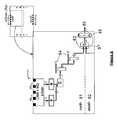
- An EHF wireless communication receiver (1)comprises a phased array radio (2) arranged for receiving a beam of incoming signals (4) in a predetermined frequency band within the EHF range.
- the radio (2)comprises a plurality of antenna paths (3), each handling one of the incoming signals (4) and forming a differential I/Q output signal (5) from the incoming signal.
- Each antenna pathcomprises I and Q branches with a downconversion part (6) for downconverting the incoming signal to baseband and a phase shifting part (7) for applying a controllable phase shift to the incoming signal.
- the radio (2)further comprises signal combination circuitry (8) connected to the antenna paths and arranged for combining the differential phase-shifted I/Q output signals to a combined differential I/Q signal and control circuitry (9) connected to the phase shifting parts of the antenna paths and arranged for controlling the controllable phase shift.
- the phase shifting partcomprises a set of variable gain amplifiers (10) arranged for applying controllable gains to the respective downconverted incoming signals in the I/Q branches.
- the receiver architectureuses direct downconversion. The beamforming is performed after direct downconversion, in the analog baseband part, where the incoming signal is present in differential I/Q format. If this operation would be performed at RF then first an I/Q signal needs to be generated, requiring extra circuitry such as a quadrature all-pass filter.
- phase shiftingis performed by multiplying the I signal and the Q signal (5) with appropriate sines and cosines of the wanted phase shift ⁇ , resulting in new, phase-shifted I and Q values.
- I ⁇cos ⁇ ⁇ I - sin ⁇ ⁇ Q
- Q ⁇sin ⁇ ⁇ I + cos ⁇ ⁇ Q
- I ⁇ Q ⁇A ⁇ cos ⁇ - A ⁇ sin ⁇ A ⁇ sin ⁇ A ⁇ cos ⁇ ⁇ I Q
- Beamforming at analog basebandhas advantages compared to beamforming operations (phase shift and summation) at RF, especially for many antenna paths. Indeed, for many antenna paths the distance between the phase shifted signals - no matter how this phase shift is implemented - and the combined output(s) is inevitably large. Bridging this distance at high frequencies can be lossy and/or power hungry when long transmission lines need to be driven, which may require several signal repeaters operating at high frequencies, which may consume much power. Furthermore, such repeaters use resonant loads which can have a passband that can be shifted in frequency by process tolerances and/or small parasitics. This can give rise to loss.
- baseband phase shiftingis more robust and compact. Indeed, at baseband there is no need for resonant circuits with bulky inductors or transmission lines. Furthermore, modeling errors on the parasitics from interconnect and from the different components play a minor role. Indeed, a few femtofarads of difference between modeling/simulation and the reality can be neglected at baseband. This makes the performance of analog baseband circuitry more predictable than mm-wave circuitry, which is also an objective advantage over phase shifting in the LO path.
- the analog baseband parthas been designed to account for the possibility of channel bonding with two channels. To this end, the bandwidth of the circuits has been made programmable.
- phase noise contributions from each VCOwhich are uncorrelated, can be averaged out, as the signal distortions caused by phase noise do not combine constructively at signal combination.
- a similar reasoningis valid for other noise sources in the PLL, except for the upconversion of phase noise from the reference frequency, which is common to all PLLs.
- phase noise of a 60 GHz PLLis not dominated by upconverted reference noise, the averaging still has effect, giving a phase noise reduction with a factor 10*log 10 (N), N being the number of antenna paths.
- one PLL per two antenna pathsis used.
- the four antenna pathsare grouped two by two, which is in correspondence with the floorplan of the example implementation in 40 nm CMOS (see Figure 6 ).
- two antenna pathsare grouped in the north of the chip (antenna path one handling RF in1 and two handling RF in2 ) and two in the south of the chip (antenna path three and four).
- the different building blockswill be briefly discussed.
- the implemented receiverhas four antenna paths which are combined at baseband, two baseband filters (namely for the combined I-path and the combined Q-path) and two PLLs.
- LNA3means the low-noise amplifier in antenna path 3.
- the two PLLsare indicated with PLL12 (belonging to antenna paths 1 and 2) and PLL34 (belonging to antenna paths 3 and 4).
- the building blocks of one those two PLLsalso get the suffix 12 and 34, respectively.
- the required phase shift to be applied in the different antenna pathsis determined in an initial step by means of procedures known to the person skilled in the art, in particular at the MAC (Medium Access Control) layer and then passed to the physical layer. This is described in [1] and [2]:
- a network-on-chipcan be implemented.
- Thisis a master-slave system, in which the master (31) is connected to the pins (32) of the chip via which the control can be brought onto the chip, while there are slave nodes (34) corresponding to a large unit of analog circuitry.
- the slave nodes (34)are put in a ring, which in turn is connected to the master node (31) (see Figure 2 ). Via a serial communication the bits can be transported to the appropriate slave nodes.
- These slave nodes (34)are digital circuits with output lines that go to the analog circuits (35).
- the control by the bits corresponding to these lineshas been implemented in different ways, depending on the requirements in the circuit. Sometimes a digital-to-analog converter (DAC) is used.
- DACdigital-to-analog converter
- Another possible implementation of digital controlis the use of different parallel transistors in the signal path, each transistor having a different width while the widths differ from each other with a factor of two.
- the NOCis schematically shown in Figure 2 .
- Only six bond pads (32)are needed for the NOC: digital VDD (1.1 V) and ground, a serial data input (DIN in Figure 2 ), a clock line (CLK), a reset (RST) and a transfer enable line (TE).
- the digital I/O padsneed two more extra bond pads, namely the power and ground connection for the 2.5 V power domain that is only used in the digital I/Os.
- the six linesare distributed to the different slave nodes (34), that are connected in a ring structure.
- Slave node ihas n i connections to the analog circuits (35).
- the layout of the master (31) and the slave nodes (34)has been generated with a digital design flow that takes as an input a bounding box for the layout as well as bit lines with names, which will be the control lines for the analog circuits (35).
- a set of spare bitsis provided, in order to allow for extra control bits which were not foreseen during specification of the NOC at the beginning of the digital synthesis.
- the phase shifterscomprise current amplifiers with variable gain.
- the same schematic of the current amplifieris reused everywhere. They have a low input impedance and a high output impedance.
- the input (in_a and in_b) of such current amplifier(see Figure 4 ) is a common-gate stage (transistors M 1a and M 1b ).
- the input impedance of the common-gate stagewhich is already low, is further lowered by an extra shunt feedback at the input (via resistors R fa and R fb ).
- the output impedanceis high by the use of a cascode stage at the output.
- the combination or summation of signalsis performed by summing currents, in front of the input of a current amplifier, as shown schematically in Figure 5 .
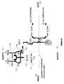
- FIG. 6A part of the floorplan of the chip is shown in Figure 6 .
- the RF input signals from the four antennasenter the chip via two sides: north (81) and south (82).
- the second combiner stage (83)sums the combined signals from the north and the south that result from the first combiner stage. There is an unavoidable and considerable distance between the RF inputs and the inputs at baseband to the channel selection filters.
- baseband signal repeaters (84)are preferably inserted in the signal path. These repeaters are preferably current amplifiers with a low input impedance.
- the second combiner stage (83)the signals from the northern and the southern part of the chip are summed in the current domain and then fed into a transimpedance amplifier (TIA), (85). This has a low input impedance and low output impedance.
- the four lines at the output of the TIA(I+, I-, Q+ and Q-) are fed to the channel selection filters (86).
- the combiner of path one and two in Figure 6is again a current amplifier at the input of which two lines, each carrying the signal current from an antenna path, are connected together.
- the summing block (87) in Figure 6 that combines the lines from the north and the south partis also implemented by connecting two lines together.
- the signal path between the output of a phase shifter and the analog baseband filters beyond the beamforming circuitrycomprises three current amplifiers, each connected with long interconnect lines.
- This ideacan be generalized, i.e. it is not restricted to three current amplifiers. The number of current amplifiers depends on the distance that needs to be bridged and the parasitic capacitance per unit length of the interconnection lines.
- the channel selection filters (86)are for example fifth-order Butterworth filters based on Sallen-Key biquads. These use unity-gain amplifiers, which comprise a low-gain differential pair followed by a super-source follower.
- the cutoff frequencycan have two values, 875 MHz and 1750 MHz, depending on whether one single channel is used or two channels are bonded together.
- a built-in self test (BIST) blockis provided.
- the calibration blockcontains a replica of a phase shifter and a transimpedance amplifier. When the parts of the calibration block are calibrated appropriately, then the same settings are used for the corresponding blocks in the signal path.
- the calibration blockuses a shift register from which data can be read. This is done by bringing a serial line off chip. To save bondpads, this serial line is multiplexed with other digital signals that are brought off chip, namely the divider outputs (at the same frequency of the reference frequency of the PLLs) of the two PLLs.
- the clock and other control signals for the shift registercome from the NOC.
- comparatorsare connected to each analog node in this block to output the DC operating points of the circuits.
- Each comparatorproduces a digital output which is then put to the shift register.
- a comparisonis made between the circuit node voltage and an external reference voltage. By sweeping the external voltage and outputting the comparison result, it is possible to obtain the DC operating point of all nodes simultaneously.
- the input capacitance of the comparatoris just the capacitance of a small inverter and therefore is negligible in the signal path.
- the conversion gainhas been simulated with in Spectre RF.
- the noise and mixerhave been put in the highest gain mode while the subsequent circuitry in which gain can still be made (from the phase shifters to the input of the channel selection filters) has been programmed such that the gain in that circuitry is 0 dB. Only one antenna path has been simulated.
- the resulting conversion gainis shown in Figure 7 .
- the LO frequencyhas been put to 61 GHz. It is found that the 3 dB bandwidth is around 700 MHz. It is mainly due to the non-flatness of the LNA gain. This will be improved in a further design.
- the LO signalhas been directly applied to the mixer input amplitude in this setup is 1 V single-ended peak to peak.
- the third-order input-referred intercept point IIP3 with this gain settingis -28 dBm.
- the total chipconsumes 398 mW.
- a pie chart of the power consumption of a complete 4-antenna receiveris shown in Figure 10 .
- the LO bufferingconsumes a large part, due to a wrong size of the transformer in the second stage of the buffer. With an optimized size of that transformer the power consumption of the LO buffers for PLL12 and PLL34 together can be reduced to 44 mW. This brings the complete power consumption to 343 mW.
- the floorplan of the four-antenna implementation in 40 nm CMOSis shown in Figure 11 .
- the RF inputsare brought on the chip via the northern (101) and the southern edges (102).
- the baseband outputsare located at the east side (103) of the chip. This allows extending the chip in the eastern direction with analog-to-digital converters and eventually a digital part.
- the western edge (104) of the chipis reserved for digital control inputs (the connections for the NOC), the reference frequency input for the PLL and some other low-frequency control data.
- the summation of the antenna paths 1 (105) and 2 (106)is performed by connecting together the output lines from the two phase shifters (107), (108), and feeding the result to a first current amplifier (109), referred to as "REP0" in Figure 11 .
- the routing of the four phases of the QVCO (110) output around 60 GHzis shorter, thanks to the use of two PLLs (111) instead of one central PLL.
- the distance between a QVCO output and the corresponding mixer (112) inputsis about 300 micrometer. This distance is bridged by the LO buffering.
- the architecture proposed here in combination with this type of floorplanis more attractive for a large number (> 4) of antenna paths, compared to a floorplan where all RF inputs would be in line, located at one of the four sides, as the chip can be better contacted from two different sides.
- the current amplifier REP41has two inputs, namely the outputs of the northern and southern REP2 cells of set 1.
- REP3ithe output of set i-1 must be routed to the east side of set i.
- REP4ian extra repeater
- the output of set Nis a transimpedance amplifier (like TIA in Figure 11 ), which has three current inputs, namely the output of REP3N and the outputs of the northern and southern REP2 cells of set N.
- the implementation shown in Figure 12performs the signal combination at baseband while bridging the interconnect distance between the signal lines of the different antenna paths at baseband, using low-input impedance current amplifiers that lead to a high bandwidth despite the parasitic capacitance of the interconnect between the repeaters.
Landscapes
- Engineering & Computer Science (AREA)
- Computer Networks & Wireless Communication (AREA)
- Signal Processing (AREA)
- Variable-Direction Aerials And Aerial Arrays (AREA)
- Radio Transmission System (AREA)
Description
- The present invention relates to an extremely high frequency (EHF) receiver according to the preamble of
claim 1. - Extremely high frequency (EHF) is the highest radio frequency band, covering the range of frequencies from 30 to 300 GHz. Compared to wireless applications operating below this band, the free space path loss is much higher. Hence, antenna arrays with beamforming are used to achieve transmission over a longer distance.
- Within the EHF band, a 7 GHz band around 60 GHz is envisaged for different emerging wireless communication applications. The number of antenna paths can be different for different applications. For distances up to 10 meter (e.g. transfer of HDTV data between a HDTV and a high-definition DVD player) an array of 16 antennas might be needed. For distances up to a few meters, less antenna paths (e.g. four) might be enough. A number of N antennas corresponds in the receiver to N antenna paths, which need to be combined. It is a challenge to combine so many paths without loss of performance.
- A 60 GHz low noise direct-downconversion front-end is known fromBorremans, J. et al, "A digitally controlled compact 57-to-66GHz front-end in 45nm digital CMOS", Solid-state Circuits Conference - Digest of Technical Papers, 2009, ISSCC 2009, IEEE International, Piscataway, NJ, USA, 8 February 2009, pp. 492-493A.
- It is an aim of this invention to provide an EHF wireless communication receiver in which the signals received on the different antenna paths can be combined with less performance degradation and lower power consumption than existing combination methods, which usually combine signals at high frequencies.
- According to the invention, this aim is achieved with the EHF wireless communication receiver showing the characteristics of the first independent claim.
- It is a further aim of this invention to provide a method for receiving an EHF wireless communication signal in which the signals received on the different antenna paths can be combined with better performance.
- According to the invention, this further aim is achieved with the method performing the steps of the second independent claim.
- In the EHF wireless communication receiver and method of the invention, the beamforming operations (phase shifting and signal combination) are performed after downconversion, i.e. at analog baseband. It has been found that this can improve performance in view of reduced losses over the parasitic capacitances and inductances of the circuitry. Furthermore, performing these operations at baseband is found to be advantageous terms of power consumption, in view of the lower frequency at which the operations are performed.
- The architecture of the present invention has the advantage of being scalable with respect to the number of antenna paths.
- In the EHF wireless communication receiver and method of the invention, the phase shifting is implemented by means of a set of variable gain amplifiers arranged for applying controllable gains to the respective downconverted incoming signals in the I/Q branches of each antenna path. The control circuitry is arranged for setting the controllable gains of the variable gain amplifiers to values that are proportional to the coefficients of a rotational matrix, by means of which the determined phase shift to achieve beamforming is applied to the respective incoming signal in the respective antenna path. This may or may not involve adding gain to the respective incoming signal on top of applying the phase shift.
- In preferred embodiments, the downconversion part is a direct downconversion part equipped for downconverting the incoming signal to baseband in a single step.
- In preferred embodiments, the phased array radio comprises multiple phase-locked loops (PLL) synchronized with each other, each phase-locked loop being connected to the downconversion part of at least one antenna path and being provided for generating a local oscillation signal therefor. The voltage-controlled oscillator (VCO) at the output of such PLL is a quadrature VCO (QVCO) that provides differential quadrature signals, which are needed for direct downconversion. The use of multiple phase-locked loops has the advantage over a common phase-locked loop for all antenna paths that the specifications on the PLL phase noise can be relaxed. For example in the case that every antenna path has its own PLL, the phase noise contributions from each VCO, which are uncorrelated, can be averaged out, as the signal distortions caused by phase noise do not combine constructively.
- Preferably, each phase-locked loop is connected to the downconversion part of at least two antenna paths, to optimally trade off phase noise performance and LO buffering requirements with power and area consumption.
- In preferred embodiments, signal repeaters are inserted in between two parts of the interconnect lines bridging the distance between the antenna paths and the place where the signals of the different antenna paths are combined. The signal repeaters may be current amplifiers. In this way, it can be avoided that the distance that must be bridged on the chip by combining many antenna paths limits the bandwidth. Thanks to the low input impedance of these current amplifiers the pole caused by the real part of the input impedance and the parasitic capacitance of the interconnect lines can be put easily beyond the bandwidth of the baseband signal. As a result, the architecture of the present invention is scalable with respect to the number of antenna paths as it is suitable for extension to many antenna paths without loss of performance due to the overhead of connecting many antenna paths together.
- In preferred embodiments, the receiver is arranged for AV-OFDM communication in the band around 60 GHz.
- The invention will be further elucidated by means of the following description and the appended drawings.
Figure 1 shows a receive architecture.Figure 2 illustrates the concept of the network on chip.Figure 3 shows a transformer used to couple the LO buffering and the mixer.Figure 4 shows a simplified schematic of the current amplifier used in the phase sifters, signal combiners and baseband signal repeaters.Figure 5 illustrates the principle of signal combination.Figure 6 shows part of the floorplan.Figure 7 plots conversion gain as a function of RF frequency.Figure 8 plots noise figure as a function of the baseband frequency.Figure 9 plots gain (left) and noise figure (right) as a function of frequency and for different LO amplitudes.Figure 10 shows a breakdown of the power consumption. Left: based on simulations of the chip. Right: idem except for the LO buffering.Figure 11 shows a floorplan of a part of the chip.Figure 12 shows a floorplan of a part of a twelve-antenna receiver.- The present invention will be described with respect to particular embodiments and with reference to certain drawings but the invention is not limited thereto but only by the claims. The drawings described are only schematic and are non-limiting. In the drawings, the size of some of the elements may be exaggerated and not drawn on scale for illustrative purposes. The dimensions and the relative dimensions do not necessarily correspond to actual reductions to practice of the invention.
- Furthermore, the terms first, second, third and the like in the description and in the claims, are used for distinguishing between similar elements and not necessarily for describing a sequential or chronological order. The terms are interchangeable under appropriate circumstances and the embodiments of the invention can operate in other sequences than described or illustrated herein.
- Moreover, the terms top, bottom, over, under and the like in the description and the claims are used for descriptive purposes and not necessarily for describing relative positions. The terms so used are interchangeable under appropriate circumstances and the embodiments of the invention described herein can operate in other orientations than described or illustrated herein.
- The term "comprising", used in the claims, should not be interpreted as being restricted to the means listed thereafter; it does not exclude other elements or steps. It needs to be interpreted as specifying the presence of the stated features, integers, steps or components as referred to, but does not preclude the presence or addition of one or more other features, integers, steps or components, or groups thereof. Thus, the scope of the expression "a device comprising means A and B" should not be limited to devices consisting only of components A and B. It means that with respect to the present invention, the only relevant components of the device are A and B.
- In particular, the invention presents a device and method for receiving RF signals within the EHF band, preferably the band around 60 GHz, in which beamforming is used. The idea is to perform the beamforming operations (phase shifting and signal combination) at analog baseband. Compared to beamforming operations at RF, beamforming operations at baseband are cheaper in terms of power consumption and give less performance degradation. Preferably, performance degradation as a result of the distance that must be bridged on the chip in the case of a large number of antenna paths is avoided by using current amplifiers in between long lines. The bandwidth limitations due to the parasitic capacitance of the long lines, are overcome thanks to the low input impedance of the current amplifiers: the real part of that impedance forms a pole with the interconnect capacitance that is beyond the envisaged signal bandwidth.
- Because the beamforming operations are performed at baseband, downconversion circuit parts are required in each antenna/signal path, which are preferably downconversion mixers which rely on local oscillator signals. The problem of distribution of a common local oscillator signal is circumvented by using multiple phase-locked loops (PLLs), e.g. one PLL per two antenna paths. The different PLLs are synchronized with respect to each other by using the same reference frequency signal. This is a low-frequency signal that can be distributed easily over long distances, which is needed in the case of many antenna paths. This approach gives less performance degradation than the use of one central PLL, which requires the distribution of a high-frequency local oscillator signal to many antenna paths (over a long distance on the chip).
- The invention will be exemplified below by a receiver design in 40 nm CMOS comprising four antenna paths but is not limited hereto. For mm-wave applications, the CMOS technologies that can be used are the 90 nm generation or below. These generations feature transistors that are fast enough to properly handle millimeter-wave signals. In the example implementation 40 nm CMOS is used. The example contains the circuitry between LNA inputs up to the output of the analog baseband filters for channel selection. The beamforming is implemented by phase shifting and signal combination at analog baseband. The downconversion is performed in one step (zero-IF).
- The performance of the different building blocks has been made digitally programmable with a so-called network on chip. With a conversion gain setting of around 30 dB, the noise figure of the receiver chip is around 8.5 dB (it changes slightly with frequency). The power consumption of the receiver chip is 398 mW. With this noise figure and when taking into account signal degradations of the antenna interface and the receive blocks behind the analog baseband filters (namely variable-gain amplifier (VGA) and the analog-to-digital converter (ADC) that has been designed standalone in e.g. 40 nm process) then with a QAM16 modulation on the OFDM carriers (requiring a signal-to-noise ratio of 20.5 dB) the complete receiver has a sensitivity level better than -50 dBm, which is the value prescribed in the 802.15.3c standard for AV-OFDM. When the power consumption of the ADC and an estimate for the VGA is taken into account, then the total receiver consumes 422 mW. From this consumption 27 % goes to LO buffering. Further simulations have shown that the power consumption of this buffering can be with 79 mW while maintaining a large output swing. This brings the power consumption of the complete receiver to 343 mW.
- The architecture of the proposed invention shows a high degree of scalability of the receiver in terms of the number of antenna paths.
- A technology that can be used is a 40 nm digital CMOS technology. It uses seven metal levels (copper) and a thick top aluminum layer.
- The receive architecture is shown in
Figure 1 . An EHF wireless communication receiver (1) comprises a phased array radio (2) arranged for receiving a beam of incoming signals (4) in a predetermined frequency band within the EHF range. The radio (2) comprises a plurality of antenna paths (3), each handling one of the incoming signals (4) and forming a differential I/Q output signal (5) from the incoming signal. Each antenna path comprises I and Q branches with a downconversion part (6) for downconverting the incoming signal to baseband and a phase shifting part (7) for applying a controllable phase shift to the incoming signal. The radio (2) further comprises signal combination circuitry (8) connected to the antenna paths and arranged for combining the differential phase-shifted I/Q output signals to a combined differential I/Q signal and control circuitry (9) connected to the phase shifting parts of the antenna paths and arranged for controlling the controllable phase shift. The phase shifting part comprises a set of variable gain amplifiers (10) arranged for applying controllable gains to the respective downconverted incoming signals in the I/Q branches. The receiver architecture uses direct downconversion. The beamforming is performed after direct downconversion, in the analog baseband part, where the incoming signal is present in differential I/Q format. If this operation would be performed at RF then first an I/Q signal needs to be generated, requiring extra circuitry such as a quadrature all-pass filter. - The phase shifting is performed by multiplying the I signal and the Q signal (5) with appropriate sines and cosines of the wanted phase shift ϕ, resulting in new, phase-shifted I and Q values. Indeed, denoting the I and Q values after phase shifting by I' and Q', they can be related to the original I and Q values as follows:

- This operation is applied to any I and Q baseband signal (5) of every antenna path (3). It is implemented using amplifiers (10) with a gain that is digitally controllable. An on-chip calibration of the phase shift is provided as well. As the output of the downconversion mixers is a current, the variable-gain amplifiers are implemented as current amplifiers. Further, some extra gain can be added to increase the signal strength at this point. This is implemented by introducing a common scale factor A in equation (1):

- This can be written in the form of a rotational matrix:

- After phase shifting, all new I' signals are summed (8), just as all new Q' signals. This summation is performed in the current domain (a summation of currents). Such summation can be made more linear than a summation of voltages.
- Beamforming at analog baseband has advantages compared to beamforming operations (phase shift and summation) at RF, especially for many antenna paths. Indeed, for many antenna paths the distance between the phase shifted signals - no matter how this phase shift is implemented - and the combined output(s) is inevitably large. Bridging this distance at high frequencies can be lossy and/or power hungry when long transmission lines need to be driven, which may require several signal repeaters operating at high frequencies, which may consume much power. Furthermore, such repeaters use resonant loads which can have a passband that can be shifted in frequency by process tolerances and/or small parasitics. This can give rise to loss.
- Compared to phase shifting at RF, baseband phase shifting is more robust and compact. Indeed, at baseband there is no need for resonant circuits with bulky inductors or transmission lines. Furthermore, modeling errors on the parasitics from interconnect and from the different components play a minor role. Indeed, a few femtofarads of difference between modeling/simulation and the reality can be neglected at baseband. This makes the performance of analog baseband circuitry more predictable than mm-wave circuitry, which is also an objective advantage over phase shifting in the LO path.
- The analog baseband part has been designed to account for the possibility of channel bonding with two channels. To this end, the bandwidth of the circuits has been made programmable.
- To relieve the specifications on the PLL phase noise, more than one PLL (11) is used. Assume that every antenna path has its own PLL (11). In that case, the phase noise contributions from each VCO, which are uncorrelated, can be averaged out, as the signal distortions caused by phase noise do not combine constructively at signal combination. A similar reasoning is valid for other noise sources in the PLL, except for the upconversion of phase noise from the reference frequency, which is common to all PLLs. However, as phase noise of a 60 GHz PLL is not dominated by upconverted reference noise, the averaging still has effect, giving a phase noise reduction with a
factor 10*log10(N), N being the number of antenna paths. - To optimally trade off phase noise performance and LO buffering requirements with power and area consumption, one can use less than N PLLs. In the receiver chip one PLL per two antenna paths is used. The four antenna paths are grouped two by two, which is in correspondence with the floorplan of the example implementation in 40 nm CMOS (see
Figure 6 ). On the chip layout two antenna paths are grouped in the north of the chip (antenna path one handling RFin1 and two handling RFin2) and two in the south of the chip (antenna path three and four). In the following sections, the different building blocks will be briefly discussed. - The implemented receiver has four antenna paths which are combined at baseband, two baseband filters (namely for the combined I-path and the combined Q-path) and two PLLs. The building blocks that belong to antenna pathi (i=1, ..., 4) geti as a suffix. For example, LNA3 means the low-noise amplifier in
antenna path 3. Further, the two PLLs are indicated with PLL12 (belonging toantenna paths 1 and 2) and PLL34 (belonging toantenna paths 3 and 4). The building blocks of one those two PLLs also get thesuffix - The required phase shift to be applied in the different antenna paths is determined in an initial step by means of procedures known to the person skilled in the art, in particular at the MAC (Medium Access Control) layer and then passed to the physical layer. This is described in [1] and [2]:
- 1. IEEE 802.15 WPAN Millimeter wave alternative PHY task group 3c (TG3c),http://www.ieee802.org/15/pub/TG3c.html.
- 2. Ecma TC48 draft standard for high rate 60 GHz WPANs, Ecma/TC48/2008/144,http://www.ecmainternational.org/publications/files/drafts/tc48-2008-144.pdf.
- To program the different analog blocks and to overcome variability issues, a network-on-chip (NOC) can be implemented. This is a master-slave system, in which the master (31) is connected to the pins (32) of the chip via which the control can be brought onto the chip, while there are slave nodes (34) corresponding to a large unit of analog circuitry. The slave nodes (34) are put in a ring, which in turn is connected to the master node (31) (see
Figure 2 ). Via a serial communication the bits can be transported to the appropriate slave nodes. These slave nodes (34) are digital circuits with output lines that go to the analog circuits (35). The control by the bits corresponding to these lines has been implemented in different ways, depending on the requirements in the circuit. Sometimes a digital-to-analog converter (DAC) is used. Another possible implementation of digital control is the use of different parallel transistors in the signal path, each transistor having a different width while the widths differ from each other with a factor of two. - The NOC is schematically shown in
Figure 2 . Only six bond pads (32) are needed for the NOC: digital VDD (1.1 V) and ground, a serial data input (DIN inFigure 2 ), a clock line (CLK), a reset (RST) and a transfer enable line (TE). The digital I/O pads need two more extra bond pads, namely the power and ground connection for the 2.5 V power domain that is only used in the digital I/Os. The six lines are distributed to the different slave nodes (34), that are connected in a ring structure. Slave nodei hasni connections to the analog circuits (35). - The layout of the master (31) and the slave nodes (34) has been generated with a digital design flow that takes as an input a bounding box for the layout as well as bit lines with names, which will be the control lines for the analog circuits (35). For each slave node (34) a set of spare bits is provided, in order to allow for extra control bits which were not foreseen during specification of the NOC at the beginning of the digital synthesis.
- In the proposed version of the NOC only bits can be entered into the chip. If desired, other solutions can be implemented (e.g. reading out bits), such as the use of shift registers, as implemented for the calibration of the phase shifters.
- The phase shifters comprise current amplifiers with variable gain. The same schematic of the current amplifier is reused everywhere. They have a low input impedance and a high output impedance. The input (in_a and in_b) of such current amplifier (see
Figure 4 ) is a common-gate stage (transistors M1a and M1b). The input impedance of the common-gate stage, which is already low, is further lowered by an extra shunt feedback at the input (via resistors Rfa and Rfb). The output impedance is high by the use of a cascode stage at the output. - The combination or summation of signals is performed by summing currents, in front of the input of a current amplifier, as shown schematically in
Figure 5 . - A part of the floorplan of the chip is shown in
Figure 6 . The RF input signals from the four antennas enter the chip via two sides: north (81) and south (82). The four signal paths are combined in two stages. Each stage combines two signals (= currents) that are in differential quadrature format. This means that in the first combiner stage, the signals frompath chip paths 
and this shifts to higher frequencies whenRin, current amp is lowered. - To further maintain the bandwidth, while bridging a long distance with signal lines, baseband signal repeaters (84) are preferably inserted in the signal path. These repeaters are preferably current amplifiers with a low input impedance.
- After the second repeater there is the second combiner stage (83): the signals from the northern and the southern part of the chip are summed in the current domain and then fed into a transimpedance amplifier (TIA), (85). This has a low input impedance and low output impedance. The four lines at the output of the TIA (I+, I-, Q+ and Q-) are fed to the channel selection filters (86). The combiner of path one and two in
Figure 6 is again a current amplifier at the input of which two lines, each carrying the signal current from an antenna path, are connected together. The summing block (87) inFigure 6 that combines the lines from the north and the south part is also implemented by connecting two lines together. This means that the signal path between the output of a phase shifter and the analog baseband filters beyond the beamforming circuitry comprises three current amplifiers, each connected with long interconnect lines. This idea can be generalized, i.e. it is not restricted to three current amplifiers. The number of current amplifiers depends on the distance that needs to be bridged and the parasitic capacitance per unit length of the interconnection lines. - The channel selection filters (86) are for example fifth-order Butterworth filters based on Sallen-Key biquads. These use unity-gain amplifiers, which comprise a low-gain differential pair followed by a super-source follower. The cutoff frequency can have two values, 875 MHz and 1750 MHz, depending on whether one single channel is used or two channels are bonded together.
- To calibrate (and/or debug) the phase shifters, a built-in self test (BIST) block is provided. The calibration block contains a replica of a phase shifter and a transimpedance amplifier. When the parts of the calibration block are calibrated appropriately, then the same settings are used for the corresponding blocks in the signal path.
- The calibration block uses a shift register from which data can be read. This is done by bringing a serial line off chip. To save bondpads, this serial line is multiplexed with other digital signals that are brought off chip, namely the divider outputs (at the same frequency of the reference frequency of the PLLs) of the two PLLs. The clock and other control signals for the shift register come from the NOC.
- In the calibration block, comparators are connected to each analog node in this block to output the DC operating points of the circuits. Each comparator produces a digital output which is then put to the shift register. A comparison is made between the circuit node voltage and an external reference voltage. By sweeping the external voltage and outputting the comparison result, it is possible to obtain the DC operating point of all nodes simultaneously. The input capacitance of the comparator is just the capacitance of a small inverter and therefore is negligible in the signal path.
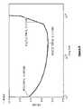
- The conversion gain has been simulated with in Spectre RF. For this simulation the noise and mixer have been put in the highest gain mode while the subsequent circuitry in which gain can still be made (from the phase shifters to the input of the channel selection filters) has been programmed such that the gain in that circuitry is 0 dB. Only one antenna path has been simulated. The resulting conversion gain is shown in
Figure 7 . For this simulation the LO frequency has been put to 61 GHz. It is found that the 3 dB bandwidth is around 700 MHz. It is mainly due to the non-flatness of the LNA gain. This will be improved in a further design. For this simulation the LO signal has been directly applied to the mixer input amplitude in this setup is 1 V single-ended peak to peak. - The corresponding noise figure is shown in
Figure 8 . As a comparison, with the cascade analysis from the architectural study, the noise figure after the lowpass filter output was found to be 8 dB. This number includes a loss of 4.5 dB in the antenna interface, a noise figure reduction of 6 dB due to the combination of the four antenna paths and 1 dB due to the contribution of phase noise. Compensating for these effects, which are not in our circuit-level simulations, we would have a value from the cascade analysis of 8 dB - 4.5 dB + 6 dB - 1dB = 8.5 dB. This is a good correspondence with the results ofFigure 8 . - The third-order input-referred intercept point IIP3 with this gain setting is -28 dBm.
- With the same gain settings, the gain and noise figure for different LO amplitudes is shown in
Figure 9 . - The total chip consumes 398 mW. To complete this to a whole receiver, we add an estimate for the power consumption of the VGAs in the I-path and the Q-path (10 mW x 2) as well as the simulated value of the ADCs in the I-path and the Q-path (0.85 µW/MHz per ADC). A pie chart of the power consumption of a complete 4-antenna receiver is shown in
Figure 10 . The LO buffering consumes a large part, due to a wrong size of the transformer in the second stage of the buffer. With an optimized size of that transformer the power consumption of the LO buffers for PLL12 and PLL34 together can be reduced to 44 mW. This brings the complete power consumption to 343 mW. - The downconversion with the phase shifters and signal combiners together consume 49 mW. This is the total cost of the baseband beamforming (phase shifting and signal combination). This type of beamforming requires less power consumption than phase shifting in the LO path combined with signal combination at baseband. Indeed, from a 45 nm design of a 4-antenna receiver with the same RF section, the same PLL (but only one PLL) but using phase shifting in the LO path, we find a power consumption for the phase shifters in the LO path (around 60 GHz) of 46 mW for four antenna paths, which is almost as much as the baseband phase shifting and signal combination together.
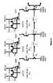
- The floorplan of the four-antenna implementation in 40 nm CMOS is shown in
Figure 11 . The RF inputs are brought on the chip via the northern (101) and the southern edges (102). The baseband outputs are located at the east side (103) of the chip. This allows extending the chip in the eastern direction with analog-to-digital converters and eventually a digital part. The western edge (104) of the chip is reserved for digital control inputs (the connections for the NOC), the reference frequency input for the PLL and some other low-frequency control data. - The summation of the antenna paths 1 (105) and 2 (106) is performed by connecting together the output lines from the two phase shifters (107), (108), and feeding the result to a first current amplifier (109), referred to as "REP0" in
Figure 11 . - With this floorplan the signal flow from RF to baseband has to take a bend of 90 degrees from the north-south direction to the east. This bend is taken at baseband and not at RF such that it does not give too many signal degradations or imbalances between the four signal lines (I+, I-, Q+, Q-).
- The routing of the four phases of the QVCO (110) output around 60 GHz is shorter, thanks to the use of two PLLs (111) instead of one central PLL. In the actual 40 nm CMOS implementation the distance between a QVCO output and the corresponding mixer (112) inputs is about 300 micrometer. This distance is bridged by the LO buffering.
- The architecture proposed here in combination with this type of floorplan is more attractive for a large number (> 4) of antenna paths, compared to a floorplan where all RF inputs would be in line, located at one of the four sides, as the chip can be better contacted from two different sides.
- An extension of the floorplan to more antenna paths is possible by putting sets of four antenna paths next to each other as shown in
Figure 12 for twelve antenna paths. Assume there are 4N antenna paths, divided into N sets of four antenna paths. We assume that the leftmost set (= the one at the largest distance from the baseband filters beyond the beamforming circuitry) has theindex 1, while the rightmost set (= the one closest to the baseband filters beyond the beamforming circuitry) has the index N. The sets are combined as follows: - At the output of
sets 1, ..., N-1 we put a current amplifier, like the repeaters "REP0", "REP1" and "REP2" inFigure 11 . This current amplifier is referred to as "REP4i" in which i is an index ranging from 1 to N-1. - The current amplifier REP41 has two inputs, namely the outputs of the northern and southern REP2 cells of
set 1. - In set i (i = 2, ..., N), the output of set i-1 must be routed to the east side of set i. In order to bridge this distance without much loss of performance, an extra repeater is provided, referred to as REP3i. For
sets 2 to N-1 the output of REP3i is fed to REP4i, which has three current inputs, namely the output of REP3i and the outputs of the northern and southern REP2 cells of set i. The output of set N is a transimpedance amplifier (like TIA inFigure 11 ), which has three current inputs, namely the output of REP3N and the outputs of the northern and southern REP2 cells of set N. - When putting several current amplifiers in cascade, the bandwidth of the cascade connection is smaller than the bandwidth of one single current amplifier. However, simulations have shown that this is not a problem to obtain a 1.75 GHz bandwidth, which is needed for bonding of two channels.
- The implementation shown in
Figure 12 performs the signal combination at baseband while bridging the interconnect distance between the signal lines of the different antenna paths at baseband, using low-input impedance current amplifiers that lead to a high bandwidth despite the parasitic capacitance of the interconnect between the repeaters.


Claims (15)
- EHF wireless communication receiver (1) comprising a phased array radio (2) arranged for receiving a beam of incoming signals in a predetermined frequency band within the EHF range, the phased array radio comprising- a plurality of antenna paths (3), each being arranged for handling one of the incoming signals (4) and forming a differential I/Q output signal (5) from the incoming signal, each antenna path comprising I and Q branches with a downconversion part (6) for downconverting the incoming signal to baseband and a phase shifting part (7) for applying a controllable phase shift to the signal of each antenna path, such that the differential I/Q output signals formed by the plurality of antenna paths are synchronized with each other;- signal combination circuitry (8) connected to the antenna paths and arranged for combining the differential I/Q output signals to a combined differential I/Q signal;- control circuitry (9) connected to the phase shifting parts of the antenna paths and arranged for controlling the controllable phase shift;characterized in that in each antenna path, the phase shifting part is a baseband part downstream from the downconversion part andin that the phase shifting part comprises a set of variable gain amplifiers (10) arranged for applying controllable gains to the respective downconverted incoming signals in the I/Q branches, the control circuitry (9) being arranged for setting the controllable gains of the variable gain amplifiers to coefficients of a rotational matrix which is determined from the phase shift to be applied to the respective incoming signal.
- EHF wireless communication receiver according to claim 1,characterized in that the rotational matrix is given by:

wherein
I andQ are in-phase and quadrature signals together forming the respective downconverted incoming signal in the I/Q branches of the respective antenna path;
I' andQ' are in-phase and quadrature signals together forming the phase-shifted, differential I/Q output signal of the respective antenna path;
A is a common scale factor for possibly adding gain to the respective incoming signal on top of applying the phase shift;
ϕ is the phase shift to be applied to the respective incoming signal of an antenna path. - EHF wireless communication receiver according to claim 1 or 2,characterized in that the downconversion part is a direct downconversion part equipped for downconverting the incoming signal to baseband in a single step.
- EHF wireless communication receiver according to any one of the previous claims,characterized in that the phased array radio comprises multiple phase-locked loops synchronized with each other, each phase-locked loop being connected to the downconversion part of at least one antenna path and being provided for generating a local oscillation signal therefor.
- EHF wireless communication receiver according to claim 4,characterized in that each phase-locked loop is connected to the downconversion part of at least two antenna paths.
- EHF wireless communication receiver according to any one of the previous claims,characterized in that the baseband signal combination circuitry comprises signal repeaters in between parts of lines bridging the distance between the antenna paths.
- EHF wireless communication receiver according to claim 6,characterized in that the signal repeaters are current amplifiers.
- EHF wireless communication receiver according to any one of the previous claims,characterized in that the receiver is arranged for AV-OFDM communication around 60 GHz.
- Method of receiving a beam of incoming signals in a predetermined frequency band within the EHF range, comprising the steps of:- supplying the incoming signals to a plurality of antenna paths, each being arranged for handling one of the incoming signals and forming a differential I/Q output signal from the incoming signal,- splitting each incoming signal to I and Q branches of each antenna path,- downconverting each incoming signal in the I and Q branches to baseband and applying a controllable phase shift to each incoming signal in the I and Q branches,- controlling the controllable phase shifts such that the differential I/Q output signals formed by the plurality of antenna paths are synchronized with each other;- combining the differential I/Q output signals to a combined differential I/Q signal;characterized in that in each antenna path, the controllable phase shift is applied after the downconversion of the incoming signal andin that the controllable phase shift is applied by applying controllable gains to the respective downconverted incoming signals in the I/Q branches, the controllable gains being set to coefficients of a rotation matrix which is determined from the phase shift to be applied to the respective incoming signal.
- Method according to claim 9,characterized in that the step of applying the phase shift comprises the step of adding gain to the downconverted signal by means of a variable gain amplifier.
- Method according to claim 9 or 10,characterized in that the rotational matrix is given by:

wherein
I andQ are in-phase and quadrature signals together forming the respective downconverted incoming signal in the I/Q branches of the respective antenna path;
I' andQ' are in-phase and quadrature signals together forming the phase-shifted, differential I/Q output signal of the respective antenna path;
A is a common scale factor for possibly adding gain to the respective incoming signal on top of applying the phase shift;
ϕ is the phase shift to be applied to the respective incoming signal. - Method according to any one of the claims 9-11,characterized in that the downconversion is performed in a single step.
- Method according to any one of the claims 9-12,characterized in that local oscillation signals in differential I/Q format are generated for each downconversion part performing the downconversion of the incoming signals, said local oscillation signals being generated by means of multiple phase-locked loops synchronized with each other.
- Method according to claim 13,characterized in that each phase-locked loop is connected to the downconversion part of at least two antenna paths.
- Method according to any one of the claims 9-14,characterized in that, the method comprises an initial step of determining the controllable phase shift to be applied to each of the antenna paths.


Priority Applications (4)
| Application Number | Priority Date | Filing Date | Title |
|---|---|---|---|
| US13/380,135US8532226B2 (en) | 2009-06-23 | 2010-06-23 | EHF wireless communication receiver using beamforming with a scalable number of antenna paths |
| PCT/EP2010/058882WO2010149689A1 (en) | 2009-06-23 | 2010-06-23 | Efh wireless communication receiver using beamforming with scalable number of antenna paths |
| JP2012516709AJP2012531159A (en) | 2009-06-23 | 2010-06-23 | EHF wireless communication receiver using beamforming with multiple extensible antenna paths |
| KR1020127001853AKR20120104143A (en) | 2009-06-23 | 2010-06-23 | Ehf wireless communication receiver using beamforming with scalable number of antenna paths |
Applications Claiming Priority (1)
| Application Number | Priority Date | Filing Date | Title |
|---|---|---|---|
| US26942909P | 2009-06-23 | 2009-06-23 |
Publications (2)
| Publication Number | Publication Date |
|---|---|
| EP2267919A1 EP2267919A1 (en) | 2010-12-29 |
| EP2267919B1true EP2267919B1 (en) | 2012-11-07 |
Family
ID=42084579
Family Applications (1)
| Application Number | Title | Priority Date | Filing Date |
|---|---|---|---|
| EP10152098AActiveEP2267919B1 (en) | 2009-06-23 | 2010-01-29 | EHF wireless communication receiver using beamforming with scalable number of antenna paths |
Country Status (5)
| Country | Link |
|---|---|
| US (1) | US8532226B2 (en) |
| EP (1) | EP2267919B1 (en) |
| JP (1) | JP2012531159A (en) |
| KR (1) | KR20120104143A (en) |
| WO (1) | WO2010149689A1 (en) |
Families Citing this family (32)
| Publication number | Priority date | Publication date | Assignee | Title |
|---|---|---|---|---|
| US8260252B2 (en) | 2006-10-02 | 2012-09-04 | The Nielsen Company (Us), Llc | Method and apparatus for collecting information about portable device usage |
| US8321556B1 (en)* | 2007-07-09 | 2012-11-27 | The Nielsen Company (Us), Llc | Method and system for collecting data on a wireless device |
| AU2009345651B2 (en) | 2009-05-08 | 2016-05-12 | Arbitron Mobile Oy | System and method for behavioural and contextual data analytics |
| CA3020551C (en) | 2010-06-24 | 2022-06-07 | Arbitron Mobile Oy | Network server arrangement for processing non-parametric, multi-dimensional, spatial and temporal human behavior or technical observations measured pervasively, and related method for the same |
| US8565798B2 (en)* | 2010-07-26 | 2013-10-22 | Rincon Research Corporation | Geo-directed adaptive antenna array |
| US8340685B2 (en) | 2010-08-25 | 2012-12-25 | The Nielsen Company (Us), Llc | Methods, systems and apparatus to generate market segmentation data with anonymous location data |
| FR2969426B1 (en)* | 2010-12-15 | 2013-08-30 | St Microelectronics Sa | CIRCUIT DEPHASAGE |
| RU2465725C1 (en)* | 2011-04-21 | 2012-10-27 | Открытое акционерное общество "Концерн "Созвездие" | Broadband system for radio communication in short-wave range |
| US8929473B2 (en)* | 2011-07-28 | 2015-01-06 | Samsung Electronics Co., Ltd. | Combining baseband processing and radio frequency beam steering in wireless communication systems |
| EP2584651B1 (en) | 2011-10-18 | 2015-07-01 | Imec | Method for beamforming and device using the same |
| US9490886B2 (en)* | 2012-02-27 | 2016-11-08 | Qualcomm Incorporated | RF beamforming in phased array application |
| EP2675080B1 (en) | 2012-06-15 | 2019-06-12 | IMEC vzw | A phased-array receiver for mm-wave applications |
| US9048928B2 (en) | 2012-11-13 | 2015-06-02 | Qualcomm Incorporated | Expandable transceivers and receivers |
| JP6021711B2 (en)* | 2013-03-28 | 2016-11-09 | 三菱電機株式会社 | Receiving apparatus and receiving method |
| US9670937B2 (en)* | 2013-05-30 | 2017-06-06 | Ingersoll-Rand Company | Centrifugal compressor having cooling system |
| US20160194949A1 (en) | 2013-10-08 | 2016-07-07 | Halliburton Energy Services, Inc. | Integrated well survey management and planning tool |
| KR101692242B1 (en)* | 2014-12-16 | 2017-01-04 | (주)에프씨아이 | Apparatus for Transmitting and Receiving Signal in Radio Frequency System |
| US9531451B2 (en) | 2015-03-19 | 2016-12-27 | Infineon Technologies Ag | System and method for high-speed analog beamforming |
| WO2016146196A1 (en) | 2015-03-19 | 2016-09-22 | Telefonaktiebolaget Lm Ericsson (Publ) | A beamforming receiver |
| WO2016146198A1 (en)* | 2015-03-19 | 2016-09-22 | Telefonaktiebolaget Lm Ericsson (Publ) | Phase rotation and amplitude control unit |
| TWI667842B (en) | 2016-04-15 | 2019-08-01 | 和碩聯合科技股份有限公司 | Antenna system and control method |
| US10250418B2 (en) | 2016-08-02 | 2019-04-02 | Keyssa Systems, Inc. | EHF receiver architecture with dynamically adjustable discrimination threshold |
| US10469112B2 (en)* | 2017-05-31 | 2019-11-05 | Silicon Laboratories Inc. | System, apparatus and method for performing automatic gain control in a receiver for a packet-based protocol |
| JP6440911B1 (en)* | 2018-02-14 | 2018-12-19 | 三菱電機株式会社 | Mixa |
| EP3557786A1 (en) | 2018-04-16 | 2019-10-23 | Samsung Electronics Co., Ltd. | Method of testing rf integrated circuit |
| JP7404680B2 (en)* | 2019-07-11 | 2023-12-26 | 富士通株式会社 | Beamforming device and beamforming method |
| WO2021090286A1 (en)* | 2019-11-08 | 2021-05-14 | Vayyar Imaging Ltd. | Systems and methods for providing wide beam radar arrays |
| JP2023510174A (en) | 2019-12-31 | 2023-03-13 | バヤー イメージング リミテッド | Systems and methods for shaping beams produced by antenna arrays |
| JP7524607B2 (en) | 2020-05-27 | 2024-07-30 | 富士通株式会社 | Wireless devices |
| JP7647297B2 (en) | 2021-04-26 | 2025-03-18 | 富士通株式会社 | Radio signal processing circuit and radio device |
| CN117118365B (en)* | 2023-10-24 | 2024-03-01 | 华南理工大学 | Millimeter wave frequency source array and wireless energy transmission equipment based on cascade phase control |
| US12334889B1 (en) | 2023-12-14 | 2025-06-17 | Silicon Laboratories Inc. | Gain contol to optimize sensitivity and blocking performance |
Family Cites Families (4)
| Publication number | Priority date | Publication date | Assignee | Title |
|---|---|---|---|---|
| US7386286B2 (en)* | 2001-06-01 | 2008-06-10 | Broadband Innovations, Inc. | High frequency low noise phase-frequency detector and phase noise reduction method and apparatus |
| JP4120237B2 (en)* | 2002-02-28 | 2008-07-16 | ソニー株式会社 | Demodulator and receiver |
| US7738583B2 (en)* | 2005-04-21 | 2010-06-15 | Broadcom Corporation | Reduced feedback for beamforming in a wireless communication |
| US8085877B2 (en)* | 2007-09-28 | 2011-12-27 | Broadcom Corporation | Method and system for quadrature local oscillator generator utilizing a DDFS for extremely high frequencies |
- 2010
- 2010-01-29EPEP10152098Apatent/EP2267919B1/enactiveActive
- 2010-06-23USUS13/380,135patent/US8532226B2/enactiveActive
- 2010-06-23WOPCT/EP2010/058882patent/WO2010149689A1/enactiveApplication Filing
- 2010-06-23JPJP2012516709Apatent/JP2012531159A/ennot_activeWithdrawn
- 2010-06-23KRKR1020127001853Apatent/KR20120104143A/ennot_activeWithdrawn
Also Published As
| Publication number | Publication date |
|---|---|
| JP2012531159A (en) | 2012-12-06 |
| US20120121043A1 (en) | 2012-05-17 |
| EP2267919A1 (en) | 2010-12-29 |
| WO2010149689A9 (en) | 2011-03-17 |
| KR20120104143A (en) | 2012-09-20 |
| US8532226B2 (en) | 2013-09-10 |
| WO2010149689A1 (en) | 2010-12-29 |
Similar Documents
| Publication | Publication Date | Title |
|---|---|---|
| EP2267919B1 (en) | EHF wireless communication receiver using beamforming with scalable number of antenna paths | |
| Okada et al. | Full four-channel 6.3-Gb/s 60-GHz CMOS transceiver with low-power analog and digital baseband circuitry | |
| US9020457B2 (en) | Phased-array receiver for mm-wave applications | |
| Koh et al. | A 6–18 GHz 5-bit active phase shifter | |
| US20130293303A1 (en) | Dual Carrier Amplifier Circuits And Methods | |
| Lin et al. | A 60GHz digitally controlled RF beamforming array in 65nm CMOS with off-chip antennas | |
| KR20160003109A (en) | Jammer resistant noise cancelling receiver front end | |
| CN103391123A (en) | Satellite-borne multi-beam receiving antenna correction system and method | |
| Beikmirza et al. | A wideband four-way Doherty bits-in RF-out CMOS transmitter | |
| Koh et al. | A $ Q $-Band Four-Element Phased-Array Front-End Receiver With Integrated Wilkinson Power Combiners in 0.18-$\mu {{\hbox {m}}} $ SiGe BiCMOS Technology | |
| US11711106B2 (en) | Multi-channel receiver and multi-channel reception method | |
| US20160028579A1 (en) | In-phase and quadrature radio frequency digital-to-analog converter | |
| KR101346449B1 (en) | Configurable antenna interface | |
| CN118554985B (en) | A transceiver multiplexing multi-beamforming chip | |
| US8942299B2 (en) | Baseband beamforming | |
| Tseng et al. | A four-channel beamforming down-converter in 90-nm CMOS utilizing phase-oversampling | |
| CN113852386B (en) | Receiver circuit and method of using receiver circuit | |
| Pang et al. | A ku-band common-leg transceiver with built-in configurable register in 130-nm CMOS technology for phased-array systems | |
| CN111952726B (en) | Multi-beam phased array chip, receiver module, and transmitter module | |
| JP2002135187A (en) | Receiver | |
| WO2014132315A1 (en) | Receiver | |
| Sah et al. | An ultra-wideband 15–35 GHz phase-shifter for beamforming applications | |
| Shaheen et al. | A fully integrated 4× 2 element CMOS RF phased array receiver for 5G | |
| Akbar et al. | A 38.5-to-60.5 GHz LNA with wideband combiner supporting cartesian beamforming architecture | |
| Krishnamurthy et al. | Integrated time division multiplexing front-end circuit for multi-antenna RF receivers |
Legal Events
| Date | Code | Title | Description |
|---|---|---|---|
| PUAI | Public reference made under article 153(3) epc to a published international application that has entered the european phase | Free format text:ORIGINAL CODE: 0009012 | |
| AK | Designated contracting states | Kind code of ref document:A1 Designated state(s):AT BE BG CH CY CZ DE DK EE ES FI FR GB GR HR HU IE IS IT LI LT LU LV MC MK MT NL NO PL PT RO SE SI SK SM TR | |
| AX | Request for extension of the european patent | Extension state:AL BA RS | |
| 17P | Request for examination filed | Effective date:20110629 | |
| GRAP | Despatch of communication of intention to grant a patent | Free format text:ORIGINAL CODE: EPIDOSNIGR1 | |
| GRAS | Grant fee paid | Free format text:ORIGINAL CODE: EPIDOSNIGR3 | |
| GRAA | (expected) grant | Free format text:ORIGINAL CODE: 0009210 | |
| AK | Designated contracting states | Kind code of ref document:B1 Designated state(s):AT BE BG CH CY CZ DE DK EE ES FI FR GB GR HR HU IE IS IT LI LT LU LV MC MK MT NL NO PL PT RO SE SI SK SM TR | |
| REG | Reference to a national code | Ref country code:GB Ref legal event code:FG4D | |
| REG | Reference to a national code | Ref country code:CH Ref legal event code:EP Ref country code:AT Ref legal event code:REF Ref document number:583355 Country of ref document:AT Kind code of ref document:T Effective date:20121115 | |
| REG | Reference to a national code | Ref country code:IE Ref legal event code:FG4D | |
| REG | Reference to a national code | Ref country code:DE Ref legal event code:R096 Ref document number:602010003477 Country of ref document:DE Effective date:20130103 | |
| REG | Reference to a national code | Ref country code:AT Ref legal event code:MK05 Ref document number:583355 Country of ref document:AT Kind code of ref document:T Effective date:20121107 | |
| REG | Reference to a national code | Ref country code:NL Ref legal event code:VDEP Effective date:20121107 | |
| REG | Reference to a national code | Ref country code:LT Ref legal event code:MG4D | |
| PG25 | Lapsed in a contracting state [announced via postgrant information from national office to epo] | Ref country code:IS Free format text:LAPSE BECAUSE OF FAILURE TO SUBMIT A TRANSLATION OF THE DESCRIPTION OR TO PAY THE FEE WITHIN THE PRESCRIBED TIME-LIMIT Effective date:20130307 Ref country code:SE Free format text:LAPSE BECAUSE OF FAILURE TO SUBMIT A TRANSLATION OF THE DESCRIPTION OR TO PAY THE FEE WITHIN THE PRESCRIBED TIME-LIMIT Effective date:20121107 Ref country code:NO Free format text:LAPSE BECAUSE OF FAILURE TO SUBMIT A TRANSLATION OF THE DESCRIPTION OR TO PAY THE FEE WITHIN THE PRESCRIBED TIME-LIMIT Effective date:20130207 Ref country code:HR Free format text:LAPSE BECAUSE OF FAILURE TO SUBMIT A TRANSLATION OF THE DESCRIPTION OR TO PAY THE FEE WITHIN THE PRESCRIBED TIME-LIMIT Effective date:20121107 Ref country code:NL Free format text:LAPSE BECAUSE OF FAILURE TO SUBMIT A TRANSLATION OF THE DESCRIPTION OR TO PAY THE FEE WITHIN THE PRESCRIBED TIME-LIMIT Effective date:20121107 Ref country code:FI Free format text:LAPSE BECAUSE OF FAILURE TO SUBMIT A TRANSLATION OF THE DESCRIPTION OR TO PAY THE FEE WITHIN THE PRESCRIBED TIME-LIMIT Effective date:20121107 Ref country code:LT Free format text:LAPSE BECAUSE OF FAILURE TO SUBMIT A TRANSLATION OF THE DESCRIPTION OR TO PAY THE FEE WITHIN THE PRESCRIBED TIME-LIMIT Effective date:20121107 | |
| PG25 | Lapsed in a contracting state [announced via postgrant information from national office to epo] | Ref country code:GR Free format text:LAPSE BECAUSE OF FAILURE TO SUBMIT A TRANSLATION OF THE DESCRIPTION OR TO PAY THE FEE WITHIN THE PRESCRIBED TIME-LIMIT Effective date:20130208 Ref country code:PT Free format text:LAPSE BECAUSE OF FAILURE TO SUBMIT A TRANSLATION OF THE DESCRIPTION OR TO PAY THE FEE WITHIN THE PRESCRIBED TIME-LIMIT Effective date:20130307 Ref country code:LV Free format text:LAPSE BECAUSE OF FAILURE TO SUBMIT A TRANSLATION OF THE DESCRIPTION OR TO PAY THE FEE WITHIN THE PRESCRIBED TIME-LIMIT Effective date:20121107 Ref country code:PL Free format text:LAPSE BECAUSE OF FAILURE TO SUBMIT A TRANSLATION OF THE DESCRIPTION OR TO PAY THE FEE WITHIN THE PRESCRIBED TIME-LIMIT Effective date:20121107 Ref country code:SI Free format text:LAPSE BECAUSE OF FAILURE TO SUBMIT A TRANSLATION OF THE DESCRIPTION OR TO PAY THE FEE WITHIN THE PRESCRIBED TIME-LIMIT Effective date:20121107 Ref country code:BE Free format text:LAPSE BECAUSE OF FAILURE TO SUBMIT A TRANSLATION OF THE DESCRIPTION OR TO PAY THE FEE WITHIN THE PRESCRIBED TIME-LIMIT Effective date:20121107 | |
| PG25 | Lapsed in a contracting state [announced via postgrant information from national office to epo] | Ref country code:AT Free format text:LAPSE BECAUSE OF FAILURE TO SUBMIT A TRANSLATION OF THE DESCRIPTION OR TO PAY THE FEE WITHIN THE PRESCRIBED TIME-LIMIT Effective date:20121107 | |
| PG25 | Lapsed in a contracting state [announced via postgrant information from national office to epo] | Ref country code:SK Free format text:LAPSE BECAUSE OF FAILURE TO SUBMIT A TRANSLATION OF THE DESCRIPTION OR TO PAY THE FEE WITHIN THE PRESCRIBED TIME-LIMIT Effective date:20121107 Ref country code:DK Free format text:LAPSE BECAUSE OF FAILURE TO SUBMIT A TRANSLATION OF THE DESCRIPTION OR TO PAY THE FEE WITHIN THE PRESCRIBED TIME-LIMIT Effective date:20121107 Ref country code:BG Free format text:LAPSE BECAUSE OF FAILURE TO SUBMIT A TRANSLATION OF THE DESCRIPTION OR TO PAY THE FEE WITHIN THE PRESCRIBED TIME-LIMIT Effective date:20130207 Ref country code:EE Free format text:LAPSE BECAUSE OF FAILURE TO SUBMIT A TRANSLATION OF THE DESCRIPTION OR TO PAY THE FEE WITHIN THE PRESCRIBED TIME-LIMIT Effective date:20121107 Ref country code:CZ Free format text:LAPSE BECAUSE OF FAILURE TO SUBMIT A TRANSLATION OF THE DESCRIPTION OR TO PAY THE FEE WITHIN THE PRESCRIBED TIME-LIMIT Effective date:20121107 | |
| PG25 | Lapsed in a contracting state [announced via postgrant information from national office to epo] | Ref country code:IT Free format text:LAPSE BECAUSE OF FAILURE TO SUBMIT A TRANSLATION OF THE DESCRIPTION OR TO PAY THE FEE WITHIN THE PRESCRIBED TIME-LIMIT Effective date:20121107 Ref country code:MC Free format text:LAPSE BECAUSE OF NON-PAYMENT OF DUE FEES Effective date:20130131 Ref country code:RO Free format text:LAPSE BECAUSE OF FAILURE TO SUBMIT A TRANSLATION OF THE DESCRIPTION OR TO PAY THE FEE WITHIN THE PRESCRIBED TIME-LIMIT Effective date:20121107 | |
| PLBE | No opposition filed within time limit | Free format text:ORIGINAL CODE: 0009261 | |
| STAA | Information on the status of an ep patent application or granted ep patent | Free format text:STATUS: NO OPPOSITION FILED WITHIN TIME LIMIT | |
| 26N | No opposition filed | Effective date:20130808 | |
| REG | Reference to a national code | Ref country code:IE Ref legal event code:MM4A | |
| PG25 | Lapsed in a contracting state [announced via postgrant information from national office to epo] | Ref country code:ES Free format text:LAPSE BECAUSE OF FAILURE TO SUBMIT A TRANSLATION OF THE DESCRIPTION OR TO PAY THE FEE WITHIN THE PRESCRIBED TIME-LIMIT Effective date:20130218 | |
| PG25 | Lapsed in a contracting state [announced via postgrant information from national office to epo] | Ref country code:CY Free format text:LAPSE BECAUSE OF FAILURE TO SUBMIT A TRANSLATION OF THE DESCRIPTION OR TO PAY THE FEE WITHIN THE PRESCRIBED TIME-LIMIT Effective date:20121107 | |
| REG | Reference to a national code | Ref country code:DE Ref legal event code:R097 Ref document number:602010003477 Country of ref document:DE Effective date:20130808 | |
| PG25 | Lapsed in a contracting state [announced via postgrant information from national office to epo] | Ref country code:IE Free format text:LAPSE BECAUSE OF NON-PAYMENT OF DUE FEES Effective date:20130129 | |
| PG25 | Lapsed in a contracting state [announced via postgrant information from national office to epo] | Ref country code:MT Free format text:LAPSE BECAUSE OF FAILURE TO SUBMIT A TRANSLATION OF THE DESCRIPTION OR TO PAY THE FEE WITHIN THE PRESCRIBED TIME-LIMIT Effective date:20121107 | |
| REG | Reference to a national code | Ref country code:CH Ref legal event code:PL | |
| PG25 | Lapsed in a contracting state [announced via postgrant information from national office to epo] | Ref country code:LI Free format text:LAPSE BECAUSE OF NON-PAYMENT OF DUE FEES Effective date:20140131 Ref country code:CH Free format text:LAPSE BECAUSE OF NON-PAYMENT OF DUE FEES Effective date:20140131 | |
| PG25 | Lapsed in a contracting state [announced via postgrant information from national office to epo] | Ref country code:SM Free format text:LAPSE BECAUSE OF FAILURE TO SUBMIT A TRANSLATION OF THE DESCRIPTION OR TO PAY THE FEE WITHIN THE PRESCRIBED TIME-LIMIT Effective date:20121107 | |
| PG25 | Lapsed in a contracting state [announced via postgrant information from national office to epo] | Ref country code:TR Free format text:LAPSE BECAUSE OF FAILURE TO SUBMIT A TRANSLATION OF THE DESCRIPTION OR TO PAY THE FEE WITHIN THE PRESCRIBED TIME-LIMIT Effective date:20121107 | |
| PG25 | Lapsed in a contracting state [announced via postgrant information from national office to epo] | Ref country code:HU Free format text:LAPSE BECAUSE OF FAILURE TO SUBMIT A TRANSLATION OF THE DESCRIPTION OR TO PAY THE FEE WITHIN THE PRESCRIBED TIME-LIMIT; INVALID AB INITIO Effective date:20100129 Ref country code:LU Free format text:LAPSE BECAUSE OF NON-PAYMENT OF DUE FEES Effective date:20130129 Ref country code:MK Free format text:LAPSE BECAUSE OF FAILURE TO SUBMIT A TRANSLATION OF THE DESCRIPTION OR TO PAY THE FEE WITHIN THE PRESCRIBED TIME-LIMIT Effective date:20121107 | |
| REG | Reference to a national code | Ref country code:FR Ref legal event code:PLFP Year of fee payment:7 | |
| REG | Reference to a national code | Ref country code:FR Ref legal event code:PLFP Year of fee payment:8 | |
| REG | Reference to a national code | Ref country code:FR Ref legal event code:PLFP Year of fee payment:9 | |
| P01 | Opt-out of the competence of the unified patent court (upc) registered | Effective date:20230513 | |
| PGFP | Annual fee paid to national office [announced via postgrant information from national office to epo] | Ref country code:GB Payment date:20241219 Year of fee payment:16 | |
| PGFP | Annual fee paid to national office [announced via postgrant information from national office to epo] | Ref country code:FR Payment date:20241220 Year of fee payment:16 | |
| PGFP | Annual fee paid to national office [announced via postgrant information from national office to epo] | Ref country code:DE Payment date:20241218 Year of fee payment:16 |