EP2264678A1 - RFID device tester and method - Google Patents
RFID device tester and methodDownload PDFInfo
- Publication number
- EP2264678A1 EP2264678A1EP10011255AEP10011255AEP2264678A1EP 2264678 A1EP2264678 A1EP 2264678A1EP 10011255 AEP10011255 AEP 10011255AEP 10011255 AEP10011255 AEP 10011255AEP 2264678 A1EP2264678 A1EP 2264678A1
- Authority
- EP
- European Patent Office
- Prior art keywords
- rfid
- rfid device
- elements
- tester
- antenna
- Prior art date
- Legal status (The legal status is an assumption and is not a legal conclusion. Google has not performed a legal analysis and makes no representation as to the accuracy of the status listed.)
- Granted
Links
Images


Classifications
- G—PHYSICS
- G06—COMPUTING OR CALCULATING; COUNTING
- G06K—GRAPHICAL DATA READING; PRESENTATION OF DATA; RECORD CARRIERS; HANDLING RECORD CARRIERS
- G06K7/00—Methods or arrangements for sensing record carriers, e.g. for reading patterns
- G06K7/10—Methods or arrangements for sensing record carriers, e.g. for reading patterns by electromagnetic radiation, e.g. optical sensing; by corpuscular radiation
- G06K7/10009—Methods or arrangements for sensing record carriers, e.g. for reading patterns by electromagnetic radiation, e.g. optical sensing; by corpuscular radiation sensing by radiation using wavelengths larger than 0.1 mm, e.g. radio-waves or microwaves
- G06K7/10366—Methods or arrangements for sensing record carriers, e.g. for reading patterns by electromagnetic radiation, e.g. optical sensing; by corpuscular radiation sensing by radiation using wavelengths larger than 0.1 mm, e.g. radio-waves or microwaves the interrogation device being adapted for miscellaneous applications
- G06K7/10465—Methods or arrangements for sensing record carriers, e.g. for reading patterns by electromagnetic radiation, e.g. optical sensing; by corpuscular radiation sensing by radiation using wavelengths larger than 0.1 mm, e.g. radio-waves or microwaves the interrogation device being adapted for miscellaneous applications the interrogation device being capable of self-diagnosis, e.g. in addition to or as part of the actual interrogation process
- G—PHYSICS
- G06—COMPUTING OR CALCULATING; COUNTING
- G06K—GRAPHICAL DATA READING; PRESENTATION OF DATA; RECORD CARRIERS; HANDLING RECORD CARRIERS
- G06K7/00—Methods or arrangements for sensing record carriers, e.g. for reading patterns
- G06K7/0008—General problems related to the reading of electronic memory record carriers, independent of its reading method, e.g. power transfer
- G—PHYSICS
- G06—COMPUTING OR CALCULATING; COUNTING
- G06K—GRAPHICAL DATA READING; PRESENTATION OF DATA; RECORD CARRIERS; HANDLING RECORD CARRIERS
- G06K7/00—Methods or arrangements for sensing record carriers, e.g. for reading patterns
- G06K7/0095—Testing the sensing arrangement, e.g. testing if a magnetic card reader, bar code reader, RFID interrogator or smart card reader functions properly
- Y—GENERAL TAGGING OF NEW TECHNOLOGICAL DEVELOPMENTS; GENERAL TAGGING OF CROSS-SECTIONAL TECHNOLOGIES SPANNING OVER SEVERAL SECTIONS OF THE IPC; TECHNICAL SUBJECTS COVERED BY FORMER USPC CROSS-REFERENCE ART COLLECTIONS [XRACs] AND DIGESTS
- Y10—TECHNICAL SUBJECTS COVERED BY FORMER USPC
- Y10T—TECHNICAL SUBJECTS COVERED BY FORMER US CLASSIFICATION
- Y10T29/00—Metal working
- Y10T29/49—Method of mechanical manufacture
- Y10T29/49002—Electrical device making
- Y10T29/49004—Electrical device making including measuring or testing of device or component part
Definitions
- This inventionrelates to the field of radio frequency identification (RFID) tag and label detection systems, and to methods of detecting and testing RFID tags and labels.
- RFIDradio frequency identification
- RFID tags and labelsare widely used to associate an object with an identification code.
- RFID devicesgenerally have a combination of antennas and analog and/or digital electronics, which may include for example communications electronics, data memory, and control logic.
- RFID tagsare used in conjunction with security-locks in cars, for access control to buildings, and for tracking inventory and parcels.
- Some examples of RFID tags and labelsappear in U.S. Patent Nos. 6,107,920 , 6,206,292 , and 6,262,292 , all of which are hereby incorporated by reference in their entireties.
- RFID devicesare generally categorized as labels or tags.
- RFID labelsare RFID devices that are adhesively or otherwise have a surface attached directly to objects.
- RFID tagsare secured to objects by other means, for example by use of a plastic fastener, string or other fastening means.
- RFID devicesinclude active tags and labels, which include a power source, and passive tags and labels, which do not.
- passive tagsin order to retrieve the information from the chip, a "base station” or “reader” sends an excitation signal to the RFID tag or label. The excitation signal energizes the tag or label, and the RFID circuitry transmits the stored information back to the reader. The "reader” receives and decodes the information from the RFID tag.
- RFID tagscan retain and transmit enough information to uniquely identify individuals, packages, inventory and the like.
- RFID tags and labelsalso can be characterized as to those to which information is written only once (although the information may be read repeatedly), and those to which information may be written during use. For example, RFID tags may store environmental data (that may be detected by an associated sensor), logistical histories, state data, etc.
- RFID devicesOne difficulty associated with RFID devices is the need to test operation of such devices as part of the manufacturing or fabrication process.
- the devicesIn fabrication of RFID devices, the devices may be formed on a sheet or roll of material, closely spaced apart.
- an antennais used to send radio frequency (RF) fields over a relatively long range, that is, over intervening free space.
- RFradio frequency
- an RFID device testeris capacitively coupled to an RFID device, in order to provide power from the tester to the device, and to receive a signal from the device to the tester.
- an RFID device testerprovides power to an RFID device to be tested, by sending an outgoing power signal that is at a frequency other than the resonant frequency of the antenna of the RFID device.
- an RFID device testerhas conductive coupling elements for capacitively coupling to antenna elements of an RFID device.
- an RFID device testerhas hoop-shaped conductive coupling elements.
- an RFID device test systemhas multiple testers operatively coupled together for testing a web of devices having rows of devices, with multiple devices in each row.
- the multiple testersmay be in a staggered configuration, rather than being in a line in the direction of the rows.
- a method of testing a radio frequency identification (RFID) deviceincludes the steps of: 1) capacitively coupling an RFID device tester to an antenna of the RFID device; 2) generating an outgoing signal from the RFID device tester; 3) using the outgoing signal to power the RFID device; 4) generating a return signal in the RFID device; and detecting a return signal, via a reader that is part of the tester.
- RFIDradio frequency identification
- a radio frequency identification (RFID) device testerincludes a reader; a pair of electrically-conductive coupling elements; a pair of transmission lines electrically connecting respective of the coupling elements to the reader; and a resistor connected to both of the transmission lines, between the reader and the coupling elements.
- RFIDradio frequency identification
- the RFID devicein a combination of a radio frequency identification (RFID) device and an RFID device tester, includes an antenna having a pair of antenna elements; and a chip operatively coupled to the antenna.
- the RFID device testerincludes a reader; and a pair of electrically-conductive coupling elements electrically connected to the reader.
- the antenna elementsare each capacitively coupled with respective of the coupling elements, thereby forming a pair of capacitors.
- a method of testing a radio frequency identification (RFID) deviceincludes the steps of: shifting an optimum operating frequency of the device from a natural resonant frequency to a shifted resonant frequency; and reading the device at a frequency other than the natural resonant frequency.
- RFIDradio frequency identification
- a method of testing a radio frequency identification (RFID) strapincludes the steps of: capacitively coupling an RFID device tester to conductive leads of the RFID strap; generating an outgoing signal from the RFID device tester; using the outgoing signal to power the RFID strap; generating a return signal in the RFID strap; and detecting a return signal, via a reader that is part of the tester.
- RFIDradio frequency identification
- a test systemfor testing a web containing multiple rows each having multiple RFID devices, includes: a proximity sensor for detecting the rows of RFID devices; a plurality of testers arrayed to test the multiple RFID devices of each of the rows; and a computer operatively coupled to the proximity sensor and the plurality of testers.
- the computerreceives signals from the proximity sensor and controls operation of testers.
- a method of testing a web of RFID devicesincludes the steps of: detecting one of the rows of the web by a proximity sensor; and testing the RFID devices of the row by use of respective testers that are operatively coupled to the proximity sensor.
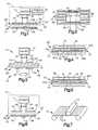
- Fig. 1is schematic side view of an RFID device tester capacitively coupled to an RFID device, in accordance with the present invention
- Fig. 2is a top view of the RFID device tester and RFID device of Fig. 1 ;
- Fig. 3is a circuit diagram illustrating the capacitive coupling of the RFID device tester and the RFID device of Fig.1 ;
- Fig. 4is a top view illustrating parts of an embodiment of the RFID device tester of Fig. 1 , which shifts the optimum operating frequency of an RFID device;
- Fig. 5is a top view illustrating parts of another embodiment of the RFID device tester of Fig. 1 , which shifts the optimum operating frequency of an RFID device;
- Fig. 6illustrates an alternate embodiment RFID device tester, capacitively coupled to an RFID device, in accordance with the present invention
- Fig. 7illustrates an RFID device tester testing a roll of RFID devices in a roll-to-roll process, in accordance with the present invention
- Fig. 8is a view illustrating another embodiment RFID device tester in accordance with the present invention.
- Fig. 9is a view illustrating yet another embodiment RFID device tester in accordance with the present invention.
- Fig. 10illustrates the RFID device tester of Fig. 9 as part of a roll-to-roll process
- Fig. 11is a top view of an RFID device test system in accordance with the present invention.
- Fig. 12is a top view of another RFID device test system in accordance with the present invention.
- Fig. 13is an oblique view of an RFID device test system in accordance with the present invention.
- Fig. 14is a plan view of the system of Fig. 13 ;
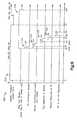
- Fig. 15is a block diagram of one embodiment of an RFID test system
- Fig. 16is a block diagram of another embodiment of an RFID test system
- Fig. 17is a block diagram of yet another embodiment of an RFID test system.
- Fig. 18is a timing diagram of part of the operation of an RFID device test system in accordance with the present invention.
- An RFID device testerincludes coupling elements for capacitively coupling a reader to an RFID device to be tested.
- the readermay power the RFID device by sending an outgoing signal, such as an outgoing AC power signal, which may be rectified and/or reflected by the RFID device, if the RFID device is operating properly.
- the outgoing signalmay have a frequency that is different from the resonant frequency of an antenna of the RFID device.
- a reader in the RFID device testerdetects the reflected and/or transmitted signal to confirm proper operation of the RFID device.
- the RFID device testermay be used as part of a roll-to-roll process, to individually test RFID devices on a roll of material. By utilizing short-range capacitive coupling, difficulties caused by simultaneous activation of multiple RFID devices may be reduced or avoided.
- an RFID device tester 10for testing or otherwise reading an RFID device 12.
- the testerincludes a reader 14, and a pair of coupling elements or couplers 16 and 18 that are electrically coupled to the reader 14.
- the coupling elements 16 and 18are electrically-conductive elements in any of a wide variety of suitable configurations.
- the coupling elements 16 and 18may be placed on a dielectric substrate layer 20.
- the tester 10may include a terminating resistor or load 24 that is connected between the coupling elements 16 and 18. As described in greater detail below, the terminating resistor 24 may function to restrict the strength of signals from the coupling elements 16 and 18 to the reader 14.
- a suitable power supply 26may be used to power the reader 14.
- the RFID device 12which may be a label or a tag, or a part of a label or a tag, has an antenna 30, and a chip 32 coupled to the antenna 30.
- the chip 32may include any of a variety of suitable electronic components, such as the circuitry described above for modulating the impedance of the RFID device 12.
- the antenna 30may be a dipole antenna having a pair of antenna elements 36 and 38 on opposite sides of the chip 32. Alternatively, the antenna 30 may have another layout.
- the antenna elements 36 and 38may be mounted on a dielectric substrate 40 of the RFID device 12.
- the dielectric substrate 40may be part of a sheet of dielectric material, such as a roll of dielectric material, upon which other RFID devices are formed.
- the other RFID devicesmay be substantially the same as, or alternatively may be different from, the RFID device 12. More specifically, the dielectric substrate may have a plurality of RFID devices closely spaced together.
- the RFID device tester 10 and the RFID device 12are capacitively coupled together, to transfer power and/or signals between the RFID device tester 10 and the RFID device 12.
- the coupling elements 16 and 18are operatively coupled to the antenna elements 36 and 38, respectively.
- This operative couplingis produced by orienting the RFID device tester 10 and the RFID device 12 such that the coupling elements 16 and 18 of the RFID device tester are substantially opposite the antenna elements 36 and 38 of the RFID device 12, as is illustrated in Figs. 1-3 . With such a relative orientation, a portion 46 of the dielectric substrate layer 20 is between the coupling element 16 and the antenna element 36, and another portion 48 of the dielectric substrate layer 20 is between the coupling element 18 and the antenna element 38.
- the coupling element 16, the antenna element 36, and the dielectric portion 46thus function as a first capacitor 50, with the coupling element 16 and the antenna element 36 being plates of the capacitor 50, and the dielectric portion 46 being the dielectric of the capacitor 50.
- the coupling element 18, the antenna element 38, and the dielectric portion 48functions as a second capacitor 52.
- the readermay send an outgoing signal, such as an outgoing AC signal, along transmission lines 56 and 58 coupling the reader 14 with the coupling elements 16 and 18.
- the capacitors 50 and 52allow transmission of the outgoing AC signal from the coupling elements 16 and 18 to the antenna elements 36 and 38.
- AC power received by the antenna elements 36 and 38may be rectified by the chip 32, for instance by transistors and/or diodes that are part of the chip 32, to produce DC power to run the chip 32.
- the powermay be used by the chip 32 to send a return signal via the antenna elements 36 and 38. It will be appreciated that the sending of the return signal may be a passive process, rather than active transmission of a return signal by the RFID device 12. As one example, circuitry in the chip 32 may be used to modulate impedance of the RFID device 12. As another example, the RFID device 12 may reflect the incident signal back to the tester 10.
- the RFID device 12either may be a passive device that automatically responds to an incident signal, or may be an active device that only responds to incident signals conforming to certain protocols.
- the RFID device 12may also have other components, such as its own power supply.
- the functioning of the RFID device 12may be substantially the same as if incident energy was provided by a long-range RF field, rather than by capacitive coupling. Alternatively, the functioning of the RFID device 12 may be different, depending upon how the incident energy is provided to it.
- the return signal generated by the RFID device 12is transmitted from the antenna elements 36 and 38 to the coupling elements 16 and 18, via the capacitors 50 and 52.
- the return signalis then forwarded to the reader 14 along the transmission lines 56 and 58.
- the terminating resistor 24may function to prevent excessively powerful signals from reaching the reader 14, and perhaps causing damage to the reader 14.
- the reader 14is able to interpret the return signal received from the RFID device 12 to confirm proper function of all or part of the RFID device 12, such as correct functioning of the antenna 30 and/or the chip 32.
- the confirming of proper functioningmay include merely detecting the presence of the RFID device 12, such that if the RFID device 12 is detectable at all, functioning of the RFID device 12 is acceptable, and the RFID device 12 passes the test.
- the testmay involve evaluation of the return signal received from the RFID device 12, for example to determine if the return signal conforms to one or more parameters or ranges of parameters. It will be appreciated that other tests of operation of the RFID device 12 may be employed, for example diagnosing faults of the RFID device 12 or otherwise qualitatively evaluating performance of the RFID device 12.
- the outgoing AC power signal sent out by the reader 14 and the return signal generated by the RFID device 12have been described above for clarity as separate signals, one sent out by the reader 14, and the other received by the reader 14.
- the signalsmay in fact be superimposed upon one another, in that the reader 14 perceives a superposition of the outgoing signal and the return signal. Therefore the interpretation of the return signal by the reader 14 may involve a comparison between the outgoing signal and the signal perceived by the reader 14, a superposition of the outgoing signal and the return signal.
- the RFID device tester 10which capacitively couples to the RFID device 12, advantageously allows short-range coupling between tester 10 and RFID device 12.
- the RFID device 12may be part of a sheet or roll having many RFID devices thereupon, and by using short-range capacitive coupling between the RFID device tester 10 and the RFID device 12, better testing of the RFID device 12 may be accomplished, compared to testers coupling to RFID devices via RF fields sent over free space.
- One reason for the advantage of the capacitively-coupling RFID device tester 10is that the short-range capacitive coupling is less prone to provide energy to other RFID devices on the same roll or sheet. By reducing or limiting the providing of energy to RFID devices other than the RFID device 12 to be tested, there is better discrimination in the testing, and thus improved testing of the RFID device 12.
- a natural resonate frequency of the antenna 30is the frequency at which the antenna 30 best receives energy from an external RF field, and at which it best sends energy, when not located in close proximity to the RFID device tester 10.
- This natural resonant frequencyis the frequency at which an antenna impedance of the antenna 30 is the complex conjugate of a chip impedance of the chip 32.
- the resonant frequencyis also referred to herein as the optimum operating point or optimum operating frequency of the RFID device 12. It will be appreciated that the resonant frequency of the antenna 30 may be highly dependent on the configuration of the antenna 30.
- the outgoing power signal from the reader 14 of the RFID device tester 10may be at a frequency that is different from the natural resonant frequency of the antenna 30 of the RFID device 12 (different from the natural optimum operating point of the RFID device 12).
- the outgoing power signal at a different frequency from the natural resonant frequency for the antenna 30 of the RFID device 12longer-range coupling may be minimized of the outgoing signals to RFID devices other than the desired RFID device 12 to be tested. This is because antennas of the RFID devices are less susceptible to receive significant amounts of power at frequencies different from the resonant frequency of the antenna 30.
- having the outgoing power signal at a different frequency than the natural resonant frequency of the antenna 30may reduce cross-coupling between the various antennas of various RFID devices on the same roll or sheet.
- Coupling between the RFID device tester 10 and the RFID device 12will itself alter the resonant frequency of the antenna 30 (the optimum operating frequency). This is because bringing the tester 10 into close proximity relative to the RFID device 12 alters the environment around the RFID device 12.
- One or more dielectric elements 60 ( Fig. 1 ) and one or more electrically-conducting elements 62 ( Fig. 1 ) of the RFID device tester 10may thereby be introduced by the tester 10 into the environment perceived by and interacting with the RFID device 12 that is being tested.
- the dielectric elements 60 and the conducting elements 62may be referred to as "shifting elements," since they function to shift or change the optimum operating frequency of the RFID device 12. As illustrated in Fig.
- the dielectric elements 60may include the dielectric substrate layer 20, and the conductor elements 62 may include the coupling elements 16 and 18. Alternatively or in addition, there may be other dielectric elements 60 and/or conductor elements 62, the latter of which may include metallic conductors. The location, size, and/or configuration of the dielectric elements 60 and/or the conductor elements 62 may be selected so as to produce a desired shift in the resonant frequency of the antenna 30.
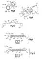
- Figs. 4 and 5show illustrative examples of parts of RFID device testers 10 with additional dielectric elements 60 and/or conductor elements 62 for shifting or altering the resonant frequency of the antenna 30 of the RFID device 12.
- the parts of the RFID device 12are shown somewhat offset from corresponding parts of the RFID device tester 10 for illustration purposes.
- Fig. 4shows parts an embodiment of the RFID device tester 10 that includes additional dielectric elements 60a and 60b that are next to the coupling elements 16 and 18.
- the dielectric elements 60a and 60bare placed over or opposite respective portions 36a and 38b of the antenna elements 36 and 38 of the antenna 30 of the RFID device 12. As shown, the dielectric elements 60a and 60b are further from the chip 32 of the RFID device 12, although it will be appreciated that other suitable configurations may be utilized.
- the dielectric elements 60a and 60bfunction to load the antenna 30 and increase the effective length of the antenna elements 36 and 38 of the antenna 30.
- an increase in effective lengthwhat is meant is that the resonant frequency or optimum operating frequency of the RFID device 12 is decreased.
- the dielectric elements 60a and 60bmay be made of a high K dielectric material, such as a suitable ceramic material.
- suitable materialsare barium tetra titanate and titanium oxide.
- Fig. 5parts of an embodiment of the RFID device tester 10 is shown that has additional electrically-conducting elements 62a and 62b, separate from the coupling elements 16 and 18, that are in close proximity to the antenna elements 36 and 38 of the antenna 30 of the RFID device 12.
- the conducting elements 62a and 62bare capacitively coupled to the antenna elements 36 and 38, increasing the effective length of the antenna elements. The resonant frequency or optimum operating point of the RFID device 12 is thereby decreased.
- the configuration of the conducting elements 62a and 62b in Fig. 5results in a decrease in the resonant frequency or optimum operating point of the RFID device 12, it will be appreciated that differently configuring the conducting elements 62a and 62b relative to the RFID device 12 may result in an increase in the resonant frequency or optimum operating point of the RFID device 12.
- the shift in resonant frequency or optimum operating point caused by the dielectric elements 60 or the conducting elements 62is localized, in that the dielectric elements 60a, 60b and/or the conducting elements 62a, 62b may be configured to shift the frequency of only a single RFID device 12, while leaving the optimum operating point of adjacent RFID devices large unaffected.
- the number and configuration of the dielectric elements 60a and 60b and the conducting elements 62a and 62bmay be varied, and may be optimized for selected antenna configurations and/or for a desired testing frequency, for example.
- the shift in the resonant frequency of the antenna 30, caused by bringing the RFID device 12 and the RFID device tester 10 together,may aid in operatively isolating the RFID device 12 from other RFID devices that may be nearby.
- By operatively isolating the RFID device 12it may be easier to test the RFID device 12 without encountering undesired results due to activation or interference from other RFID devices that are not presently being tested.
- the RFID device 12 to be testedmay be closer than other RFID devices to the dielectric elements 60 and the conducting elements 62, resonant frequency shifts of the other RFID devices may be substantially reduced in magnitude or avoided altogether, when compared with the resonant frequency shift of the RFID device 12 to be tested.
- the shift in resonant frequency occasioned by the dielectric elements 60 and/or the conducting elements 62may be substantially or largely limited to a single RFID device, the RFID device 12 to be tested.
- the dielectric elements 60 and/or the conducting elements 62may be suitably configured so as to shift an antenna having an optimum operating frequency of 915 MHz to an optimum operating frequency of 2450 MHz.
- testingmay be accomplished by shifting the optimum operating frequency of one or more RFID devices, and then testing RFID device(s).
- the device(s) testedmay be (as described above) one or more RFID devices that have had their optimum operating frequency shifted.
- testingmay be performed on one or more devices with unshifted frequencies (normal, typical, or usual frequencies), with other untested RFID devices having frequencies shifted.
- the RFID device tester 10may have multiple parts, with for example the dielectric elements 60 and/or the conducting elements 62 separate from other parts of the tester 10.
- the tester operating frequency of the RFID device tester 10may be selected so as to provide sufficient energy to activate the RFID device 12 that is being tested, and avoiding providing substantial amounts of energy to other RFID devices that may otherwise produce signals interfering with test results.
- the tester operating frequencymay be different from the natural resonant frequency of the antenna 30, and/or may be substantially the same as the new resonant frequency of the antenna 30 (the resonant frequency of the antenna 30 as shifted due to its proximity to the RFID device tester 10).
- the tester operating frequencymay be selected from a broad range of suitable RF frequencies for operatively coupling the tester 10 and the RFID device 12.
- the RF frequencies utilizedmay be greater than or less than the antenna natural frequency and/or the new antenna resonant frequency (shifted due to the proximity of the tester 10 to the RFID device 12). It will be appreciated, however, that RF frequencies that stray too far from the new antenna resonant frequency (shifted optimum operating frequency) may be unsuitable.
- there may be a lower limit for suitable RF frequenciesdue to increases in impedance of capacitive paths, for a given coupling area, as frequencies are reduced. This increase in impedance may make it more difficult to send power into the chip.
- internal rectifiers in the chip 32may have an integrating filter after them, to aid in creating the DC power supply to run the chip 32. If the frequency of the incident RF energy received from the tester 10 is too low, the filter may be unable to adequately smooth the rectified waveform output from the rectifiers. The result may be an unacceptable DC power supply for the chip 32.
- RF frequenciesthere also may be an upper limit for suitable RF frequencies for the operating frequency for the tester 10. As frequency increases, rectifier efficiency within the chip 32 decreases, reducing the fraction of input energy that is converted to DC energy to run the chip 32. Another reason for an upper limit for suitable operating frequencies is that the chip 32 may have a large input capacitance that acts as a voltage divider in conjunction with the coupling capacitors 50 and 52. As frequency of the incoming signal is increased, it therefore becomes more difficult to coupled power into the RFID device 12.
- the coupling elements 16 and 18may be 3mm ⁇ 20mm plates.
- the separation distance between the coupling elements 16 and 18 and the antenna elements 36 and 38may be about 0.2 mm.
- the capacitance of each of the capacitors 50 and 52is 7.97pF.
- the coupling elements 16 and 18are shown in Fig. 1 as approximately the same size as the corresponding antenna elements 36 and 38. It will be appreciated, however, that coupling elements 16 and 18 may be larger or smaller than the antenna elements 36 and 38 (for example as shown in Fig. 2 ).
- the RFID device tester 10may have other components in addition to those shown and described above.
- the outgoing AC power signalmay include sending signals along the transmission lines 56 and 58 that are 180 degrees out of phase with each other.
- a balance transformermay be utilized to produce the out of phase RF signals.
- the RFID device tester 10may have a matching network between the reader 14 and the transmission lines 56 and 58.
- the matching networkmay be utilized to change the impedance of the signal transmitted from the reader 14 to the transmission lines 56 and 58.
- the characteristic impedance of the reader 14may be on the order of 50 ohms, while the desired impedance of the field set up by the transmission lines 56 and 58 may be 200 ohms.
- the matching networkmay be used to shift the impedance of the signal from the reader 14 to the desired impedance for the transmission lines 56 and 58.
- Fig. 6shows an alternative relative orientation between the RFID device tester 10 and the RFID device 12, in which the RFID device 12 is inverted as compared to the orientation shown in Figs. 1 and 2 ; and described above.
- portions of the dielectric substrate 40 of the RFID device 12act as the dielectric of the capacitors 50 and 52.
- the dielectric layer 20 of the RFID device tester 10( Fig. 1 ) may thus be omitted.
- an air gapmay be used as the dielectric for the capacitors 50 and 52.
- the RFID device tester 10 and/or the RFID device 12may have structures or other elements to maintain a repeatable air gap between the coupling elements 16 and 18 of the RFID device tester 10, and the antenna elements 36 and 38 of the RFID device 12.
- the RFID device tester 10may be utilized in a roll-to-roll process to test a plurality of RFID devices 12 that are parts of or are on a roll material 70.
- the tester 10may be fixed in location, with the various RFID devices 12 being tested one at a time as they move past the tester 10.
- the roll material 70may be appropriately driven to move the RFID devices 12 past the tester 10.
- the RFID devices 12may move continuously past the tester 10, or alternatively each of the RFID devices 12 may pause to be tested as it passes under the RFID device tester 10.
- the RFID device tester 10may be coupled to a computer or other device for recording results of the testing of the various RFID devices, and for enabling the devices to be matched up with their test results.
- roll-to-roll fabrication processes for producing RFID devicesmay include many well-known steps, such as depositing various layers (e.g., adhesive layers, metal layers, and/or printable layers), modifying the layers (e.g., selectively removing parts of a metal layer to create an antenna), and/or depositing various components (e.g., a chip). Further details regarding roll-to-roll fabrication processes for RFID devices may be found in U.S. Patent No. 6,451,154 , which is hereby incorporated by reference in its entirety.
- FIG. 8Another alternative configuration for the RFID device tester 10 is shown in Fig. 8 , wherein the coupling elements 16 and 18 and dielectric layers 20a and 20b covering the coupling elements 16 and 18, are parts of the wheels 76 and 78.
- the coupling elements 16 and 18 and the dielectric layers 20a and 20bmay be annular or hoop-shaped.
- the coupling elements 16 and 18may be coupled to the reader 14 in a manner similar to the coupling described above with regard to other embodiments.
- the RFID device tester 10 shown in Fig. 8may be rolled over a stationary sheet or roll of material having a plurality of RFID devices 12 to be tested. Alternatively, the RFID device tester 10 may be kept stationary as the sheet or roll of RFID devices 12 moves, in contact with the wheels 76 and 78. The device tester 10 may advantageously help maintain a consistent distance between the coupling elements 16 and 18 of the tester 10, and the antenna elements 36 and 38 of the RFID device 12.
- FIGs. 9 and 10Yet another alternative configuration for the RFID device tester 10 is shown in Figs. 9 and 10 .
- the tester 10 shown in Fig. 9allows for testing of RFID devices 12 in a roll-to-roll process, with the RFID devices 12 being in a fixed relationship in close proximity to a pair of coupling elements for a minimum amount of time, even while the roll material 70 is constantly in motion.
- the tester 10 shown in Fig. 9advantageously enables testing of multiple RFID devices 12 at one time.
- the tester 10includes a roller 80 that has multiple pairs of coupling elements 16a, 18a; 16b, 18b; and 16c, 18c thereupon or therein, along or on an outer surface 82 of the roller 80.
- the roll material 70with various RFID devices 12 thereupon, winds around the roller 80.
- the outer surface 82 of the roller 80moves at the same speed as the roll material 70, such that the roll material 70 does not substantially slip relative to the roller 80.
- the RFID device 12thus maintains its position relative the corresponding pair of coupling elements 16c and 18c, for a certain coupling time period (as long as the part of the roll material 70 with the RFID device 12 is in contact with the outer surface 82 of the roller 80).
- the RFID device 12may thus be suitably coupled to a corresponding pair of coupling elements 16c and 18c, for a coupling time period.
- the rotation speed of the roller 80 and the roll material 70may be selected such that the coupling time is sufficient to allow for testing of the RFID device 18. It will also be appreciated that, for a given rotation speed, use of a larger diameter roller results in a longer coupling time.
- the various coupling elements 16a-c and 18a-care coupled to a reader 14 having multiple outputs, via a rotary joint 86. It will be appreciated that pairs of coupling elements may be evenly spaced around the outer surface 82 of the roller 80, at a spacing corresponding to the spacing of the RFID devices 12 on the roll material 70. Having multiple pairs of coupling elements on the roller 80 may enable testing of multiple RFID devices 12 simultaneously, which advantageously speeds the testing process.
- the roll material 70may move from a supply roll 90 to a take-up roll 92.
- Rollers 96 and 98may be used in conjunction with the roller 80 to maintain a portion of the roll material 70 against the roller 80.
- the roll material 70may be moved from the supply roll 90 to the take-up roll 92 by one or more suitable motors driving one or more of the rollers 80, 96, and 98, and/or one or both of the rolls 90 and 92.
- the configuration of the rolls 90 and 92, and the rollers 80, 96, and 92, shown in Fig. 10is an illustration of one of a large variety of suitable configurations, which may include other rollers, mechanisms, and/or devices.
- an RFID tester in the configuration employed in Fig. 9may have coils as part of its coupling elements 16a-c, 18a-c, and thus may be able to test RFID devices that are not high-frequency devices.
- the testermay be configured to test 13.56 MHz RFID devices.
- the coupling between the pairs of coupling elements 16a-c, 18a-cmay be capacitive, or alternatively may be by another suitable mechanism.
- RFID device tester 10may also be employed as readers, to detect the presence of RFID devices 12 or to otherwise receive information from RFID devices 12.
- a capacitively coupling RFID device tester/readersuch as described above may have a variety of suitable configurations.
- the RFID device tester/readermay have suitably-shaped slots or other openings for receiving RFID devices to be tested or read, or for receiving objects having RFID devices attached or otherwise coupled thereto.
- the RFID devicemay be a part of a tag or label.
- the RFID devicemay be a RFID strap having a chip attached to conductive leads that do not function as a conventional antenna.
- Examplesinclude an RFID strap available from Alien Technologies, and the strap marketed under the name I-CONNECT, available from Philips Electronics.
- the various embodiments of the testermay be suitable for use in testing a roll of RFID straps, with conductive elements of the RFID tester placed in proximity to the conductive leads of the RFID strap.
- the RFID device test system 110includes an RF tester 120 and a test fixture 124.
- the test fixture 124includes shifting elements 126 for shifting or changing the resonant frequency or optimum operating frequency of an RFID device 12 that is in close proximity to the test fixture 124.
- the shifting elements 126may include dielectric elements 128a and 128b ( Fig. 11 ) for decreasing effective length of the antenna elements 36 and 38 of the RFID device 12.
- the shifting elements 126may include electrically-conducting elements 130a and 130b ( Fig. 12 ) for increasing effective length of the antenna elements 36 and 38 of the RFID device 12.
- test fixture 124may shift the resonant frequency or optimum operating frequency of the RFID device 12 in a manner similar to that of the RFID devices testers 10 shown in Figs. 4 and 5 , and described above. This shifting of resonant frequency or optimum operating frequency may be localized, and may be substantially limited to a single RFID device 12 on a roll or sheet 134 of RFID devices. Thus the test fixture 124 may enable RFID devices to be tested singularly, despite their close proximity to other substantially-identical RFID devices.
- the RF tester 120may be a conventional RF reader for reading RFID devices through generation of a relatively long-range RF field, and detection of changes in the RF field that occur due to the presence of an RFID device within the field. Further information regarding suitable RF readers may be found in U.S. Patent Nos. 5,621,199 and 6,172,609 , both of which are incorporated herein by reference in their entirety.
- the RFID device 12may be tested by having the RF reader 120 emit energy at a frequency corresponding to the shifted resonant frequency or optimum operating frequency of the RFID device 12 in the test fixture 124. Since this frequency is different from the natural resonant frequency of other RFID device on the roll or sheet 134, substantial coupling with the RF tester 120 may be confined to the single RFID device 12 that is being tested. After testing, the sheet or roll 134 may be shifted relative to the test fixture 124, allowing testing of another RFID device. Thus long-range non-capacitive coupling may be used to couple to individual RFID devices on a sheet or roll of such devices.
- the RFID device test systems 110 shown in Figs. 11 and 12may be modified, as suitable, in manners similar to the various modifications described for the RFID device testers 10.
- the test fixture 124may be incorporated into a roller, to facilitate sing the RFID device test system 110 as part of a roll-to-roll process.
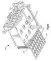
- Figs. 13 and 14show one example of an RFID device test system 200 for testing a web 202 of RFID devices or inlays 204.
- the test system 200includes a proximity sensor 210 for detecting the location of rows of the RFID devices 204 as the web 202 passed through the test system 200.
- the proximity sensor 210may include one or more elements that detect the presence of electrically-conductive material on the web 202, thereby detecting RFID devices 204.
- the test system 200also includes a number of testers 212 in a staggered configuration, and a number of markers 214 for marking RFID devices 204 that fail in testing.
- the testers 212execute a performance test on each of the RFID devices 204.
- the testers 212may utilize capacitive coupling, such as described above.
- the staggering of the testers 212allows sufficient separation to allow the testing of individual RFID devices 204 without interference without between various of the testers 212.
- the testers 212By placing the testers 212 in a staggered configuration, instead of next to one another in a row (for instance), the testers 212 have increased distance from one another, facilitating their operative isolation from one another.
- the staggered configuration of the testers 212may allow staggered timing of the testing by the various testers 212. With adjacent testers 212 operating at different times, the possibility of interference between adjacent testers is reduced, further enhancing the operative isolation of the testers 212.
- the proximity sensor 210detects the leading edge of each row of the RFID devices 204.
- the proximity sensor 210is operatively coupled to the testers 212 to trigger, at appropriate times, the testers 212 to test the RFID devices 204.
- the results of the testing by the testers 212are utilized by the markers 214 to selectively mark some of the RFID devices 204, for example by marking the RFID devices 204 that fail the testing by, for example, not demonstrating operation within acceptable parameters.
- the testingmay include a qualitative test of the RFID devices or inlays 204.
- the markers 214may include suitable ink jet markers.
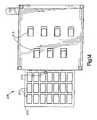
- Fig. 15shows an example of the operative parts of the test system 200.
- the proximity sensor 210 and the testers 212are operatively coupled together via a computer 220, such as a suitable personal computer, through the use of suitable input/output cards.
- the proximity sensor 210includes a pair of individual sensors 222 and 224 coupled to a proximity sensor card 226, which includes a proximity sensor power supply and proximity sensor input/output.
- the proximity sensors 222 and 224may be Keyence ED-130U proximity sensors, wired together in the "and" configuration.
- Another example of a suitable proximity sensoris a proximity sensor available from Turck.
- the proximity sensor card 226may be a suitable RS-232 card.
- the computer 220may be any of a wide variety of suitable computing systems capable of receiving and sending signals for controlling operation of the test system 200. In addition to controlling operations of the testers 212, the computer 220 may perform other functions, such as recording the results of the testing, for example by maintaining a log of serial numbers of conforming RFID devices or inlays. The computer 220 may be provided with suitable software to accomplish its purposes.
- the computermay have any a wide variety of devices coupled thereto or a part thereof.
- the computer 220may include a keyboard, mouse, or other device for allowing entry of data and/or allowing control of computer operations by a user.
- the computer 220may include a display showing, for example, status of testing operations and/or results of testing.
- the testers 212include test dipoles 230 coupled to a suitable switch 234, which in turn is coupled to the computer 220. Coaxial cables or other suitable conductors 236 may be used to coupled the test dipoles 230 to the switch 234.
- the switch 234controls timing of the testing utilizing the various testers 212, for example controlling the timing of the sending of the signals along the test dipoles 230, to capacitively couple the test dipoles 230 to the RFID devices 204.
- the computer 220uses information from the proximity sensor 210 to control the timing of the testing, in order to assure that the RFID devices 204 are appropriately located relative to the test dipoles 230 during the testing, and to control the input to an RFID device reader 238.
- FIG. 15allows coupling of multiple test dipoles 230 to the reader 238, allowing the testing of multiple RFID devices 204, in multiple columns, with a single reader.
- Fig. 16another possible configuration of the test system 200 is shown.
- the device reader 238has multiple inputs, so that it can be directly coupled to multiple dipoles 230.
- the test system 200may be capable of reading about 200 RFID devices every second, one RFID tag ever 5 ms.
- Fig. 17shows yet another configuration of the test system 200.
- the system 200includes a pair of computers 240 and 242, each coupled to a respective PCI card 244 and 246.
- the cards 244 and 246are each coupled to multiple testers 212.
- a suitable choice for the testers 212is available from Feig Electronic.
- the computers 240 and 242are also coupled to respective proximity sensors 250 and 252.
- Fig. 18shows a timing diagram 300 for one possibility of timing of the system 200.
- the proximity sensor 210registers an input 304 indicating detection of an inlay on the web 202.
- the sensor input 304defines a test window 308.
- the tester 200performs various operations: a command 310 from the computer 220 to the reader 238; transmission 314 from the reader 238 to one of the dipoles 230; a response 318 from the inlay of the RFID device 204; transmission 322 of the response from the reader 238 to the computer; and, if applicable, sending a signal from the computer 220 to the markers 214 for marking a RFID device that has failed a test.
- a method of testing a radio frequency identification (RFID) devicecomprises: capacitively coupling an RFID device tester to an antenna of the RFID device; generating an outgoing signal from the RFID device tester; using the outgoing signal to power the RFID device; generating a return signal in the RFID device; and detecting a return signal, via a reader that is part of the tester.
- the generating the outgoing signalincludes generating the outgoing signal at a signal frequency that is different from a natural resonant frequency of the antenna.
- the methodfurther comprises, prior to the generating, shifting an optimum operating frequency of the antenna from the natural resonant frequency of the antenna to a shifted resonant frequency.
- the shifting the optimum operating frequencyincludes decreasing the optimum operating frequency.
- the decreasing the optimum operating frequencyincludes bringing dielectric elements in close proximity to the antenna elements.
- the decreasing the optimum operating frequencypreferably includes overlapping portions of the antenna elements with dielectric elements.
- the dielectric elementsinclude a ceramic material.
- the ceramic materialincludes a material selected from the group consisting of barium tetra titanate and titanium oxide.
- the decreasing the optimum operating frequencypreferably includes bringing electrically-conducting elements in close proximity to the antenna elements.
- the shifting the optimum operating frequencyincludes preferably increasing the optimum operating frequency.
- the increasing the optimum operating frequencyincludes bringing electrically-conducting elements in close proximity to antenna elements of the antenna.
- the shiftingpreferably includes bringing the RFID device and at least part of the tester in close proximity.
- the generating the signal frequencypreferably includes generating a frequency that is substantially the same as the shifted resonant frequency.
- the RFID device testerincludes coupling elements electrically connected to the reader; wherein the antenna of the RFID device includes antenna elements; and wherein the capacitively coupling includes aligning the coupling elements with respective of the antenna elements.
- the coupling elementsare attached to a dielectric layer ; and wherein the aligning includes having portions of the dielectric layer between the coupling elements and the antenna elements.
- the coupling elementspreferably are part of a roller; wherein the RFID device is part of a roll material; and wherein the aligning includes bringing the portion of the roll material having the RFID device into alignment with the coupling elements as the roller rotates.
- the aligningis part of a roll-to-roll process.
- the RFID devicepreferably, is part of a sheet or roll with other RFID devices thereupon.
- the capacitively couplingincludes shifting the relative positions of the RFID device tester and the sheet or roll.
- the shiftingincludes moving the sheet or roll.
- the sheet or rollis a roll; and the moving the roll, preferably, is part of a roll-to-roll process.
- the shiftingpreferably includes moving the RFID device tester.
- the RFID device testerhas circular coupling elements, wherein the moving the RFID device tester includes rolling the RFID device tester over the sheet or roll.
- the detecting the return signalpreferably, includes: capacitively transmitting the return signal from the antenna to coupling elements of the RFID device tester; and forwarding the return signal from the coupling elements to the reader.
- the forwardingincludes forwarding the return signal past a resistor coupled to a pair of transmission lines electrically connecting the reader and respective of the coupling elements.
- a method of testing a radio frequency identification(RFID) strapcomprises: capacitively coupling an RFID device tester to conductive leads of the RFID strap; generating an outgoing signal from the RFID device tester; using the outgoing signal to power the RFID strap; generating a return signal in the RFID strap; and detecting a return signal, via a reader that is part of the tester.
- a radio frequency identification (RFID) device testercomprises: a reader; a pair of electrically-conductive coupling elements; a pair of transmission lines electrically connecting respective of the coupling elements to the reader; and a resistor connected to both of the transmission lines, between the reader and the coupling elements.
- the device testerfurther comprises dielectric materials on outer surfaces of each of the coupling elements.
- the dielectric materialsare portions of a dielectric layer.
- the coupling elementspreferably are substantially planar.
- the coupling elementspreferably are hoop- shaped.
- the device testerfurther comprises dielectric elements for shifting an optimum operating frequency of RFID devices placed in close proximity to the device tester.
- the dielectric elementsinclude ceramic elements.
- the device testerfurther comprises additional electrically-conducting elements for shifting an optimum operating frequency of RFID devices placed in close proximity to the device tester.
- the device testeris provided in combination with an RFID device, wherein the RFID device includes an antenna that is capacitively coupled to the coupling elements.
- the coupling elementsare part of a roller.
- the coupling elementsare on an outer surface of the roller.
- the device testerfurther comprises additional pairs of coupling elements on the outer surface of the roller, wherein the additional pairs of coupling elements are also coupled to the reader.
- the pairs of coupling elementsare substantially evenly circumferentially spaced about the outer surface of the roller.
- the antennaincludes a pair of antenna elements; and wherein each of the antenna elements is capacitively coupled to respective of the coupling elements.
- a radio frequency identification (RFID) device and an RFID device testercomprises: the RFID device, which includes: an antenna having a pair of antenna elements; and a chip operatively coupled to the antenna; and the RFID device tester, which includes: a reader; and a pair of electrically-conductive coupling elements electrically connected to the reader; wherein the antenna elements are each capacitively coupled with respective of the coupling elements, thereby forming a pair of capacitors.
- the combinationfurther comprises dielectric materials; wherein the dielectric materials are parts of the capacitors, between the coupling element and the antenna element of respective of the capacitors.
- the dielectric materialsare parts of the RFID device. In another preferred implementation the dielectric materials are parts of the RFID device tester.
- the dielectric materialsare portions of a unitary dielectric layer.
- the combinationfurther comprises: respective transmission lines electrically connecting the coupling elements to the reader; and a resistor between the transmission lines.
- the RFIDis part of a web of RFID devices.
- the RFID device testeris operatively coupled to a proximity sensor that senses the presence of conductive material.
- the RFID device testeris operatively coupled to a marker for selectively making RFID devices.
- a method of testing a radio frequency identification (RFID) devicecomprises: shifting an optimum operating frequency of the device from a natural resonant frequency to a shifted resonant frequency; and reading the device at a frequency other than the natural resonant frequency.
- the readingincludes reading the device at about the shifted resonant frequency.
- the shiftingincludes placing the device in close proximity to shifting elements that shift the optimum operating frequency.
- the shifting elementsinclude dielectric elements. More preferably, the dielectric elements preferably include a ceramic material.
- the shifting elementsinclude electrically-conducting elements.
- the shifting elementsare parts of an RFID device tester that also performs the reading of the device.
- the readingincludes capacitively coupling the tester and the device.
- the shifting elementsare part of a test fixture that is separate from an RFID device tester that performs the reading of the device.
- the readingincludes radio frequency coupling a reader to the device.
- the RFID deviceincludes an antenna with antenna elements; and the shifting preferably includes at least partially overlapping the antenna elements with the shifting elements.
- the shiftingincludes capacitively coupling the shifting elements to an antenna of the device.
- the device a tested RFID deviceis on a sheet or roll with other RFID devices; and wherein the placing includes placing the shifting elements closer to the tested RFID device than to any of the other RFID devices.
- a test systemfor testing a web containing multiple rows each having multiple RFID devices, the test system comprising: a proximity sensor for detecting the rows of RFID devices; a plurality of testers arrayed to test the multiple RFID devices of each of the rows; and a computer operatively coupled to the proximity sensor and the plurality of testers; wherein the computer receives signals from the proximity sensor and controls operation of testers.
- the testersare capacitively coupled to the RFID devices during testing.
- the testerseach include a pair of conductive elements configured to be in proximity to the web.
- the test systemfurther comprises one or more markers operatively coupled to the computer, for selectively marking the RFID devices based on the testing by the testers.
- the makersinclude ink jet markers.
- the testersare in a staggered configuration relative to the web, such that different of the RFID devices of one of the rows pass in proximity to respective of the testers at different times.
- the proximity sensorsincludes a sensor configured to detect presence of electrically-conductive material on a portion of the web.
- a method of testing a web of RFID devicescomprising: detecting one of the rows of the web by a proximity sensor; and testing the RFID devices of the row by use of respective testers that are operatively coupled to the proximity sensor.
- the testingincludes capacitively coupling the testers to respective of the RFID devices of the row.
- the testersare in a staggered configuration relative to the web; and wherein the testing includes testing different of the RFID devices of the row at different times.
- the methodfurther comprises selectively marking the RFID devices that fail the testing.
- the markingincludes marking with one or more ink jet markers.
- the proximity sensor and the testersare operatively coupled to a computer that receives signals from the proximity sensor and sends control signals to the testers.
Landscapes
- Engineering & Computer Science (AREA)
- Physics & Mathematics (AREA)
- Artificial Intelligence (AREA)
- Computer Vision & Pattern Recognition (AREA)
- General Physics & Mathematics (AREA)
- Theoretical Computer Science (AREA)
- Health & Medical Sciences (AREA)
- Toxicology (AREA)
- Biomedical Technology (AREA)
- Electromagnetism (AREA)
- General Health & Medical Sciences (AREA)
- Near-Field Transmission Systems (AREA)
- Details Of Aerials (AREA)
- Monitoring And Testing Of Transmission In General (AREA)
- Transceivers (AREA)
- Design And Manufacture Of Integrated Circuits (AREA)
- Testing Electric Properties And Detecting Electric Faults (AREA)
Abstract
Description
- This invention relates to the field of radio frequency identification (RFID) tag and label detection systems, and to methods of detecting and testing RFID tags and labels.
- Radio frequency identification (RFID) tags and labels (collectively referred to herein as "devices") are widely used to associate an object with an identification code. RFID devices generally have a combination of antennas and analog and/or digital electronics, which may include for example communications electronics, data memory, and control logic. For example, RFID tags are used in conjunction with security-locks in cars, for access control to buildings, and for tracking inventory and parcels. Some examples of RFID tags and labels appear in
U.S. Patent Nos. 6,107,920 ,6,206,292 , and6,262,292 , all of which are hereby incorporated by reference in their entireties. - As noted above, RFID devices are generally categorized as labels or tags. RFID labels are RFID devices that are adhesively or otherwise have a surface attached directly to objects. RFID tags, in contrast, are secured to objects by other means, for example by use of a plastic fastener, string or other fastening means.
- RFID devices include active tags and labels, which include a power source, and passive tags and labels, which do not. In the case of passive tags, in order to retrieve the information from the chip, a "base station" or "reader" sends an excitation signal to the RFID tag or label. The excitation signal energizes the tag or label, and the RFID circuitry transmits the stored information back to the reader. The "reader" receives and decodes the information from the RFID tag. In general, RFID tags can retain and transmit enough information to uniquely identify individuals, packages, inventory and the like. RFID tags and labels also can be characterized as to those to which information is written only once (although the information may be read repeatedly), and those to which information may be written during use. For example, RFID tags may store environmental data (that may be detected by an associated sensor), logistical histories, state data, etc.
- One difficulty associated with RFID devices is the need to test operation of such devices as part of the manufacturing or fabrication process. In fabrication of RFID devices, the devices may be formed on a sheet or roll of material, closely spaced apart. In traditional methods of activating, reading, and/or detecting RFID devices, an antenna is used to send radio frequency (RF) fields over a relatively long range, that is, over intervening free space. When such methods are applied to testing closely-spaced RFID devices, it is difficult to test a single RFID device, since the RF field interacts with several devices simultaneously, and the various RFID devices may interact with one another.
- In addition, it will be appreciated that lost-cost methods of reading RFID devices are desirable.
- From the foregoing it will thus be appreciated that improvements in RFID device testing and reading would be desirable.
- According to an aspect of the invention, an RFID device tester is capacitively coupled to an RFID device, in order to provide power from the tester to the device, and to receive a signal from the device to the tester.
- According to another aspect of the invention, an RFID device tester provides power to an RFID device to be tested, by sending an outgoing power signal that is at a frequency other than the resonant frequency of the antenna of the RFID device.
- According to yet another aspect of the invention, an RFID device tester has conductive coupling elements for capacitively coupling to antenna elements of an RFID device.
- According to still another aspect of the invention, an RFID device tester has hoop-shaped conductive coupling elements.
- According to another aspect of the invention, an RFID device test system has multiple testers operatively coupled together for testing a web of devices having rows of devices, with multiple devices in each row. According to an embodiment of the invention, the multiple testers may be in a staggered configuration, rather than being in a line in the direction of the rows.
- According to a further aspect of the invention, a method of testing a radio frequency identification (RFID) device, includes the steps of: 1) capacitively coupling an RFID device tester to an antenna of the RFID device; 2) generating an outgoing signal from the RFID device tester; 3) using the outgoing signal to power the RFID device; 4) generating a return signal in the RFID device; and detecting a return signal, via a reader that is part of the tester.
- According to a still further aspect of the invention, a radio frequency identification (RFID) device tester includes a reader; a pair of electrically-conductive coupling elements; a pair of transmission lines electrically connecting respective of the coupling elements to the reader; and a resistor connected to both of the transmission lines, between the reader and the coupling elements.
- According to another aspect of the invention, in a combination of a radio frequency identification (RFID) device and an RFID device tester, the RFID device includes an antenna having a pair of antenna elements; and a chip operatively coupled to the antenna. The RFID device tester includes a reader; and a pair of electrically-conductive coupling elements electrically connected to the reader. The antenna elements are each capacitively coupled with respective of the coupling elements, thereby forming a pair of capacitors.
- According to yet another aspect of the invention, a method of testing a radio frequency identification (RFID) device includes the steps of: shifting an optimum operating frequency of the device from a natural resonant frequency to a shifted resonant frequency; and reading the device at a frequency other than the natural resonant frequency.
- According to still another aspect of the invention, a method of testing a radio frequency identification (RFID) strap includes the steps of: capacitively coupling an RFID device tester to conductive leads of the RFID strap; generating an outgoing signal from the RFID device tester; using the outgoing signal to power the RFID strap; generating a return signal in the RFID strap; and detecting a return signal, via a reader that is part of the tester.
- According to a further aspect of the invention, a test system, for testing a web containing multiple rows each having multiple RFID devices, includes: a proximity sensor for detecting the rows of RFID devices; a plurality of testers arrayed to test the multiple RFID devices of each of the rows; and a computer operatively coupled to the proximity sensor and the plurality of testers. The computer receives signals from the proximity sensor and controls operation of testers.
- According to a still further aspect of the invention, a method of testing a web of RFID devices, the web including multiple rows each having multiple of the RFID devices, includes the steps of: detecting one of the rows of the web by a proximity sensor; and testing the RFID devices of the row by use of respective testers that are operatively coupled to the proximity sensor.
- To the accomplishment of the foregoing and related ends, the invention comprises the features hereinafter fully described and particularly pointed out in the claims. The following description and the annexed drawings set forth in detail certain illustrative embodiments of the invention. These embodiments are indicative, however, of but a few of the various ways in which the principles of the invention may be employed. Other objects, advantages and novel features of the invention will become apparent from the following detailed description of the invention when considered in conjunction with the drawings.
- In the annexed drawings, which are not necessarily to scale:
Fig. 1 is schematic side view of an RFID device tester capacitively coupled to an RFID device, in accordance with the present invention;Fig. 2 is a top view of the RFID device tester and RFID device ofFig. 1 ;Fig. 3 is a circuit diagram illustrating the capacitive coupling of the RFID device tester and the RFID device ofFig.1 ;Fig. 4 is a top view illustrating parts of an embodiment of the RFID device tester ofFig. 1 , which shifts the optimum operating frequency of an RFID device;Fig. 5 is a top view illustrating parts of another embodiment of the RFID device tester ofFig. 1 , which shifts the optimum operating frequency of an RFID device;Fig. 6 illustrates an alternate embodiment RFID device tester, capacitively coupled to an RFID device, in accordance with the present invention;Fig. 7 illustrates an RFID device tester testing a roll of RFID devices in a roll-to-roll process, in accordance with the present invention;Fig. 8 is a view illustrating another embodiment RFID device tester in accordance with the present invention;Fig. 9 is a view illustrating yet another embodiment RFID device tester in accordance with the present invention;Fig. 10 illustrates the RFID device tester ofFig. 9 as part of a roll-to-roll process;Fig. 11 is a top view of an RFID device test system in accordance with the present invention;Fig. 12 is a top view of another RFID device test system in accordance with the present invention;Fig. 13 is an oblique view of an RFID device test system in accordance with the present invention;Fig. 14 is a plan view of the system ofFig. 13 ;Fig. 15 is a block diagram of one embodiment of an RFID test system;Fig. 16 is a block diagram of another embodiment of an RFID test system;Fig. 17 is a block diagram of yet another embodiment of an RFID test system; andFig. 18 is a timing diagram of part of the operation of an RFID device test system in accordance with the present invention.- An RFID device tester includes coupling elements for capacitively coupling a reader to an RFID device to be tested. The reader may power the RFID device by sending an outgoing signal, such as an outgoing AC power signal, which may be rectified and/or reflected by the RFID device, if the RFID device is operating properly. The outgoing signal may have a frequency that is different from the resonant frequency of an antenna of the RFID device. A reader in the RFID device tester detects the reflected and/or transmitted signal to confirm proper operation of the RFID device. The RFID device tester may be used as part of a roll-to-roll process, to individually test RFID devices on a roll of material. By utilizing short-range capacitive coupling, difficulties caused by simultaneous activation of multiple RFID devices may be reduced or avoided.
- Referring initially to
Figs. 1 and 2 , illustrated is anRFID device tester 10 for testing or otherwise reading anRFID device 12. The tester includes areader 14, and a pair of coupling elements orcouplers reader 14. Thecoupling elements coupling elements dielectric substrate layer 20. In addition, thetester 10 may include a terminating resistor or load 24 that is connected between thecoupling elements resistor 24 may function to restrict the strength of signals from thecoupling elements reader 14. Asuitable power supply 26 may be used to power thereader 14. - The
RFID device 12, which may be a label or a tag, or a part of a label or a tag, has anantenna 30, and achip 32 coupled to theantenna 30. Thechip 32 may include any of a variety of suitable electronic components, such as the circuitry described above for modulating the impedance of theRFID device 12. Theantenna 30 may be a dipole antenna having a pair ofantenna elements chip 32. Alternatively, theantenna 30 may have another layout. Theantenna elements dielectric substrate 40 of theRFID device 12. Thedielectric substrate 40 may be part of a sheet of dielectric material, such as a roll of dielectric material, upon which other RFID devices are formed. The other RFID devices may be substantially the same as, or alternatively may be different from, theRFID device 12. More specifically, the dielectric substrate may have a plurality of RFID devices closely spaced together. - Making reference now also to
Fig. 3 , theRFID device tester 10 and theRFID device 12 are capacitively coupled together, to transfer power and/or signals between theRFID device tester 10 and theRFID device 12. Thecoupling elements antenna elements RFID device tester 10 and theRFID device 12 such that thecoupling elements antenna elements RFID device 12, as is illustrated inFigs. 1-3 . With such a relative orientation, aportion 46 of thedielectric substrate layer 20 is between thecoupling element 16 and theantenna element 36, and another portion 48 of thedielectric substrate layer 20 is between thecoupling element 18 and theantenna element 38. Thecoupling element 16, theantenna element 36, and thedielectric portion 46 thus function as afirst capacitor 50, with thecoupling element 16 and theantenna element 36 being plates of thecapacitor 50, and thedielectric portion 46 being the dielectric of thecapacitor 50. Similarly, thecoupling element 18, theantenna element 38, and the dielectric portion 48 functions as asecond capacitor 52. - Once the
RFID device tester 10 and theRFID device 12 are capacitively coupled together, electrical power and/or signals may be transferred between the two. The reader may send an outgoing signal, such as an outgoing AC signal, alongtransmission lines reader 14 with thecoupling elements capacitors coupling elements antenna elements antenna elements chip 32, for instance by transistors and/or diodes that are part of thechip 32, to produce DC power to run thechip 32. - The power may be used by the
chip 32 to send a return signal via theantenna elements RFID device 12. As one example, circuitry in thechip 32 may be used to modulate impedance of theRFID device 12. As another example, theRFID device 12 may reflect the incident signal back to thetester 10. - It will be appreciated that the
RFID device 12 either may be a passive device that automatically responds to an incident signal, or may be an active device that only responds to incident signals conforming to certain protocols. TheRFID device 12 may also have other components, such as its own power supply. - It will be further appreciated that the functioning of the
RFID device 12 may be substantially the same as if incident energy was provided by a long-range RF field, rather than by capacitive coupling. Alternatively, the functioning of theRFID device 12 may be different, depending upon how the incident energy is provided to it. - The return signal generated by the
RFID device 12 is transmitted from theantenna elements coupling elements capacitors reader 14 along thetransmission lines resistor 24 may function to prevent excessively powerful signals from reaching thereader 14, and perhaps causing damage to thereader 14. - The
reader 14 is able to interpret the return signal received from theRFID device 12 to confirm proper function of all or part of theRFID device 12, such as correct functioning of theantenna 30 and/or thechip 32. The confirming of proper functioning may include merely detecting the presence of theRFID device 12, such that if theRFID device 12 is detectable at all, functioning of theRFID device 12 is acceptable, and theRFID device 12 passes the test. Alternatively, the test may involve evaluation of the return signal received from theRFID device 12, for example to determine if the return signal conforms to one or more parameters or ranges of parameters. It will be appreciated that other tests of operation of theRFID device 12 may be employed, for example diagnosing faults of theRFID device 12 or otherwise qualitatively evaluating performance of theRFID device 12. - The outgoing AC power signal sent out by the
reader 14 and the return signal generated by theRFID device 12 have been described above for clarity as separate signals, one sent out by thereader 14, and the other received by thereader 14. In actuality, it will be appreciated that the signals may in fact be superimposed upon one another, in that thereader 14 perceives a superposition of the outgoing signal and the return signal. Therefore the interpretation of the return signal by thereader 14 may involve a comparison between the outgoing signal and the signal perceived by thereader 14, a superposition of the outgoing signal and the return signal. - The
RFID device tester 10, which capacitively couples to theRFID device 12, advantageously allows short-range coupling betweentester 10 andRFID device 12. TheRFID device 12 may be part of a sheet or roll having many RFID devices thereupon, and by using short-range capacitive coupling between theRFID device tester 10 and theRFID device 12, better testing of theRFID device 12 may be accomplished, compared to testers coupling to RFID devices via RF fields sent over free space. One reason for the advantage of the capacitively-couplingRFID device tester 10 is that the short-range capacitive coupling is less prone to provide energy to other RFID devices on the same roll or sheet. By reducing or limiting the providing of energy to RFID devices other than theRFID device 12 to be tested, there is better discrimination in the testing, and thus improved testing of theRFID device 12. - Appropriately selection of the frequency of the outgoing signal from the
tester 10 may allow further reduction in undesired coupling to RFID devices other than theRFID device 12 that is being tested. In explaining this further, it will be useful to define a natural resonate frequency of theantenna 30 as the frequency at which theantenna 30 best receives energy from an external RF field, and at which it best sends energy, when not located in close proximity to theRFID device tester 10. This natural resonant frequency is the frequency at which an antenna impedance of theantenna 30 is the complex conjugate of a chip impedance of thechip 32. The resonant frequency is also referred to herein as the optimum operating point or optimum operating frequency of theRFID device 12. It will be appreciated that the resonant frequency of theantenna 30 may be highly dependent on the configuration of theantenna 30. - One advantage of the
RFID device tester 10, which capacitively couples to theRFID device 12, is that the outgoing power signal from thereader 14 of theRFID device tester 10 may be at a frequency that is different from the natural resonant frequency of theantenna 30 of the RFID device 12 (different from the natural optimum operating point of the RFID device 12). By having the outgoing power signal at a different frequency from the natural resonant frequency for theantenna 30 of theRFID device 12, longer-range coupling may be minimized of the outgoing signals to RFID devices other than the desiredRFID device 12 to be tested. This is because antennas of the RFID devices are less susceptible to receive significant amounts of power at frequencies different from the resonant frequency of theantenna 30. Further, having the outgoing power signal at a different frequency than the natural resonant frequency of theantenna 30 may reduce cross-coupling between the various antennas of various RFID devices on the same roll or sheet. - Coupling between the
RFID device tester 10 and theRFID device 12 will itself alter the resonant frequency of the antenna 30 (the optimum operating frequency). This is because bringing thetester 10 into close proximity relative to theRFID device 12 alters the environment around theRFID device 12. One or more dielectric elements 60 (Fig. 1 ) and one or more electrically-conducting elements 62 (Fig. 1 ) of theRFID device tester 10 may thereby be introduced by thetester 10 into the environment perceived by and interacting with theRFID device 12 that is being tested. Thedielectric elements 60 and the conductingelements 62 may be referred to as "shifting elements," since they function to shift or change the optimum operating frequency of theRFID device 12. As illustrated inFig. 1 , thedielectric elements 60 may include thedielectric substrate layer 20, and theconductor elements 62 may include thecoupling elements dielectric elements 60 and/orconductor elements 62, the latter of which may include metallic conductors. The location, size, and/or configuration of thedielectric elements 60 and/or theconductor elements 62 may be selected so as to produce a desired shift in the resonant frequency of theantenna 30. Figs. 4 and 5 show illustrative examples of parts ofRFID device testers 10 with additionaldielectric elements 60 and/orconductor elements 62 for shifting or altering the resonant frequency of theantenna 30 of theRFID device 12. InFigs. 4 and 5 the parts of theRFID device 12 are shown somewhat offset from corresponding parts of theRFID device tester 10 for illustration purposes.Fig. 4 shows parts an embodiment of theRFID device tester 10 that includes additionaldielectric elements coupling elements dielectric elements respective portions 36a and 38b of theantenna elements antenna 30 of theRFID device 12. As shown, thedielectric elements chip 32 of theRFID device 12, although it will be appreciated that other suitable configurations may be utilized.- The
dielectric elements antenna 30 and increase the effective length of theantenna elements antenna 30. By an increase in effective length, what is meant is that the resonant frequency or optimum operating frequency of theRFID device 12 is decreased. - The
dielectric elements - Turning to
Fig. 5 , parts of an embodiment of theRFID device tester 10 is shown that has additional electrically-conductingelements coupling elements antenna elements antenna 30 of theRFID device 12. The conductingelements antenna elements RFID device 12 is thereby decreased. - Although the configuration of the conducting
elements Fig. 5 results in a decrease in the resonant frequency or optimum operating point of theRFID device 12, it will be appreciated that differently configuring the conductingelements RFID device 12 may result in an increase in the resonant frequency or optimum operating point of theRFID device 12. - The shift in resonant frequency or optimum operating point caused by the
dielectric elements 60 or the conductingelements 62 is localized, in that thedielectric elements elements single RFID device 12, while leaving the optimum operating point of adjacent RFID devices large unaffected. - It will appreciated that the number and configuration of the
dielectric elements elements - The shift in the resonant frequency of the
antenna 30, caused by bringing theRFID device 12 and theRFID device tester 10 together, may aid in operatively isolating theRFID device 12 from other RFID devices that may be nearby. By operatively isolating theRFID device 12, it may be easier to test theRFID device 12 without encountering undesired results due to activation or interference from other RFID devices that are not presently being tested. Since theRFID device 12 to be tested may be closer than other RFID devices to thedielectric elements 60 and the conductingelements 62, resonant frequency shifts of the other RFID devices may be substantially reduced in magnitude or avoided altogether, when compared with the resonant frequency shift of theRFID device 12 to be tested. Put another way, the shift in resonant frequency occasioned by thedielectric elements 60 and/or the conductingelements 62 may be substantially or largely limited to a single RFID device, theRFID device 12 to be tested. - As an example, the
dielectric elements 60 and/or the conductingelements 62 may be suitably configured so as to shift an antenna having an optimum operating frequency of 915 MHz to an optimum operating frequency of 2450 MHz. - It will be appreciated that the above-described concept of shift optimum operating frequency of the
RFID device 12 is but one example of a broader concept. More broadly, testing may be accomplished by shifting the optimum operating frequency of one or more RFID devices, and then testing RFID device(s). The device(s) tested may be (as described above) one or more RFID devices that have had their optimum operating frequency shifted. Alternatively, testing may be performed on one or more devices with unshifted frequencies (normal, typical, or usual frequencies), with other untested RFID devices having frequencies shifted. - It will further be appreciated that different optimum operating frequency shifts may be provided to different RFID devices to be tested. Varying the frequency shift for different RFID devices may facilitate testing multiple RFID devices simultaneously.
- In addition, it will be appreciated that the
RFID device tester 10 may have multiple parts, with for example thedielectric elements 60 and/or the conductingelements 62 separate from other parts of thetester 10. - The tester operating frequency of the
RFID device tester 10 may be selected so as to provide sufficient energy to activate theRFID device 12 that is being tested, and avoiding providing substantial amounts of energy to other RFID devices that may otherwise produce signals interfering with test results. As suggested by the above discussion, the tester operating frequency may be different from the natural resonant frequency of theantenna 30, and/or may be substantially the same as the new resonant frequency of the antenna 30 (the resonant frequency of theantenna 30 as shifted due to its proximity to the RFID device tester 10). - Alternatively, the tester operating frequency may be selected from a broad range of suitable RF frequencies for operatively coupling the
tester 10 and theRFID device 12. The RF frequencies utilized may be greater than or less than the antenna natural frequency and/or the new antenna resonant frequency (shifted due to the proximity of thetester 10 to the RFID device 12). It will be appreciated, however, that RF frequencies that stray too far from the new antenna resonant frequency (shifted optimum operating frequency) may be unsuitable. For example, there may be a lower limit for suitable RF frequencies due to increases in impedance of capacitive paths, for a given coupling area, as frequencies are reduced. This increase in impedance may make it more difficult to send power into the chip. As another example of a reason for a lower frequency limit, internal rectifiers in thechip 32 may have an integrating filter after them, to aid in creating the DC power supply to run thechip 32. If the frequency of the incident RF energy received from thetester 10 is too low, the filter may be unable to adequately smooth the rectified waveform output from the rectifiers. The result may be an unacceptable DC power supply for thechip 32. - There also may be an upper limit for suitable RF frequencies for the operating frequency for the
tester 10. As frequency increases, rectifier efficiency within thechip 32 decreases, reducing the fraction of input energy that is converted to DC energy to run thechip 32. Another reason for an upper limit for suitable operating frequencies is that thechip 32 may have a large input capacitance that acts as a voltage divider in conjunction with thecoupling capacitors RFID device 12. - According to a specific example, the
coupling elements coupling elements antenna elements capacitors - The
coupling elements Fig. 1 as approximately the same size as the correspondingantenna elements coupling elements antenna elements 36 and 38 (for example as shown inFig. 2 ). - It will be appreciated that the
RFID device tester 10 may have other components in addition to those shown and described above. For example, the outgoing AC power signal may include sending signals along thetransmission lines - As another example, the
RFID device tester 10 may have a matching network between thereader 14 and thetransmission lines reader 14 to thetransmission lines reader 14 may be on the order of 50 ohms, while the desired impedance of the field set up by thetransmission lines reader 14 to the desired impedance for thetransmission lines Fig. 6 shows an alternative relative orientation between theRFID device tester 10 and theRFID device 12, in which theRFID device 12 is inverted as compared to the orientation shown inFigs. 1 and 2 ; and described above. In the configuration shown inFig. 6 , portions of thedielectric substrate 40 of theRFID device 12 act as the dielectric of thecapacitors dielectric layer 20 of the RFID device tester 10 (Fig. 1 ) may thus be omitted.- As a further alternative, it will be appreciated that an air gap may be used as the dielectric for the
capacitors RFID device tester 10 and/or theRFID device 12 may have structures or other elements to maintain a repeatable air gap between thecoupling elements RFID device tester 10, and theantenna elements RFID device 12. - Turning now to
Fig. 7 , theRFID device tester 10 may be utilized in a roll-to-roll process to test a plurality ofRFID devices 12 that are parts of or are on aroll material 70. Thetester 10 may be fixed in location, with thevarious RFID devices 12 being tested one at a time as they move past thetester 10. Theroll material 70 may be appropriately driven to move theRFID devices 12 past thetester 10. TheRFID devices 12 may move continuously past thetester 10, or alternatively each of theRFID devices 12 may pause to be tested as it passes under theRFID device tester 10. TheRFID device tester 10 may be coupled to a computer or other device for recording results of the testing of the various RFID devices, and for enabling the devices to be matched up with their test results. - The roll-to-roll process illustrated in
Fig. 7 may be part of or may be operatively coupled with a larger roll-to-roll process for fabricating RFID devices. It will be appreciated that roll-to-roll fabrication processes for producing RFID devices may include many well-known steps, such as depositing various layers (e.g., adhesive layers, metal layers, and/or printable layers), modifying the layers (e.g., selectively removing parts of a metal layer to create an antenna), and/or depositing various components (e.g., a chip). Further details regarding roll-to-roll fabrication processes for RFID devices may be found inU.S. Patent No. 6,451,154 , which is hereby incorporated by reference in its entirety. - Another alternative configuration for the
RFID device tester 10 is shown inFig. 8 , wherein thecoupling elements dielectric layers 20a and 20b covering thecoupling elements wheels coupling elements dielectric layers 20a and 20b may be annular or hoop-shaped. Thecoupling elements reader 14 in a manner similar to the coupling described above with regard to other embodiments. - The
RFID device tester 10 shown inFig. 8 may be rolled over a stationary sheet or roll of material having a plurality ofRFID devices 12 to be tested. Alternatively, theRFID device tester 10 may be kept stationary as the sheet or roll ofRFID devices 12 moves, in contact with thewheels device tester 10 may advantageously help maintain a consistent distance between thecoupling elements tester 10, and theantenna elements RFID device 12. - Yet another alternative configuration for the
RFID device tester 10 is shown inFigs. 9 and 10 . Thetester 10 shown inFig. 9 allows for testing ofRFID devices 12 in a roll-to-roll process, with theRFID devices 12 being in a fixed relationship in close proximity to a pair of coupling elements for a minimum amount of time, even while theroll material 70 is constantly in motion. In addition, thetester 10 shown inFig. 9 advantageously enables testing ofmultiple RFID devices 12 at one time. - As shown in
Fig. 9 , thetester 10 includes aroller 80 that has multiple pairs ofcoupling elements 16a, 18a; 16b, 18b; and 16c, 18c thereupon or therein, along or on anouter surface 82 of theroller 80. Theroll material 70, withvarious RFID devices 12 thereupon, winds around theroller 80. Theouter surface 82 of theroller 80 moves at the same speed as theroll material 70, such that theroll material 70 does not substantially slip relative to theroller 80. It will be appreciated that theRFID device 12 thus maintains its position relative the corresponding pair ofcoupling elements 16c and 18c, for a certain coupling time period (as long as the part of theroll material 70 with theRFID device 12 is in contact with theouter surface 82 of the roller 80). TheRFID device 12 may thus be suitably coupled to a corresponding pair ofcoupling elements 16c and 18c, for a coupling time period. - The rotation speed of the
roller 80 and theroll material 70 may be selected such that the coupling time is sufficient to allow for testing of theRFID device 18. It will also be appreciated that, for a given rotation speed, use of a larger diameter roller results in a longer coupling time. - The
various coupling elements 16a-c and 18a-c are coupled to areader 14 having multiple outputs, via a rotary joint 86. It will be appreciated that pairs of coupling elements may be evenly spaced around theouter surface 82 of theroller 80, at a spacing corresponding to the spacing of theRFID devices 12 on theroll material 70. Having multiple pairs of coupling elements on theroller 80 may enable testing ofmultiple RFID devices 12 simultaneously, which advantageously speeds the testing process. - Referring to
Fig. 10 , theroll material 70 may move from a supply roll 90 to a take-up roll 92.Rollers roller 80 to maintain a portion of theroll material 70 against theroller 80. Theroll material 70 may be moved from the supply roll 90 to the take-up roll 92 by one or more suitable motors driving one or more of therollers rolls 90 and 92. - The configuration of the
rolls 90 and 92, and therollers Fig. 10 , is an illustration of one of a large variety of suitable configurations, which may include other rollers, mechanisms, and/or devices. - It will be appreciated that an RFID tester in the configuration employed in
Fig. 9 may have coils as part of itscoupling elements 16a-c, 18a-c, and thus may be able to test RFID devices that are not high-frequency devices. For example, the tester may be configured to test 13.56 MHz RFID devices. Thus the coupling between the pairs ofcoupling elements 16a-c, 18a-c may be capacitive, or alternatively may be by another suitable mechanism. - It will be appreciated that the various embodiments of the
RFID device tester 10 may also be employed as readers, to detect the presence ofRFID devices 12 or to otherwise receive information fromRFID devices 12. - It will further be appreciated that a capacitively coupling RFID device tester/reader such as described above may have a variety of suitable configurations. For example, the RFID device tester/reader may have suitably-shaped slots or other openings for receiving RFID devices to be tested or read, or for receiving objects having RFID devices attached or otherwise coupled thereto.
- As noted above, the RFID device may be a part of a tag or label. For example, the RFID device may be a RFID strap having a chip attached to conductive leads that do not function as a conventional antenna. Examples include an RFID strap available from Alien Technologies, and the strap marketed under the name I-CONNECT, available from Philips Electronics. Thus the various embodiments of the tester may be suitable for use in testing a roll of RFID straps, with conductive elements of the RFID tester placed in proximity to the conductive leads of the RFID strap.
- In
Figs. 11 and 12 embodiments of an RFIDdevice test system 110 are shown. The RFIDdevice test system 110 includes anRF tester 120 and atest fixture 124. Thetest fixture 124 includes shiftingelements 126 for shifting or changing the resonant frequency or optimum operating frequency of anRFID device 12 that is in close proximity to thetest fixture 124. The shiftingelements 126 may includedielectric elements Fig. 11 ) for decreasing effective length of theantenna elements RFID device 12. Alternatively, the shiftingelements 126 may include electrically-conductingelements Fig. 12 ) for increasing effective length of theantenna elements RFID device 12. Thus thetest fixture 124 may shift the resonant frequency or optimum operating frequency of theRFID device 12 in a manner similar to that of theRFID devices testers 10 shown inFigs. 4 and 5 , and described above. This shifting of resonant frequency or optimum operating frequency may be localized, and may be substantially limited to asingle RFID device 12 on a roll or sheet 134 of RFID devices. Thus thetest fixture 124 may enable RFID devices to be tested singularly, despite their close proximity to other substantially-identical RFID devices. - The
RF tester 120 may be a conventional RF reader for reading RFID devices through generation of a relatively long-range RF field, and detection of changes in the RF field that occur due to the presence of an RFID device within the field. Further information regarding suitable RF readers may be found inU.S. Patent Nos. 5,621,199 and6,172,609 , both of which are incorporated herein by reference in their entirety. - The
RFID device 12 may be tested by having theRF reader 120 emit energy at a frequency corresponding to the shifted resonant frequency or optimum operating frequency of theRFID device 12 in thetest fixture 124. Since this frequency is different from the natural resonant frequency of other RFID device on the roll or sheet 134, substantial coupling with theRF tester 120 may be confined to thesingle RFID device 12 that is being tested. After testing, the sheet or roll 134 may be shifted relative to thetest fixture 124, allowing testing of another RFID device. Thus long-range non-capacitive coupling may be used to couple to individual RFID devices on a sheet or roll of such devices. - It will be appreciated that the RFID
device test systems 110 shown inFigs. 11 and 12 may be modified, as suitable, in manners similar to the various modifications described for theRFID device testers 10. For example, thetest fixture 124 may be incorporated into a roller, to facilitate sing the RFIDdevice test system 110 as part of a roll-to-roll process. Figs. 13 and14 show one example of an RFIDdevice test system 200 for testing aweb 202 of RFID devices or inlays 204. Thetest system 200 includes aproximity sensor 210 for detecting the location of rows of theRFID devices 204 as theweb 202 passed through thetest system 200. Theproximity sensor 210 may include one or more elements that detect the presence of electrically-conductive material on theweb 202, thereby detectingRFID devices 204.- The
test system 200 also includes a number oftesters 212 in a staggered configuration, and a number ofmarkers 214 for markingRFID devices 204 that fail in testing. Thetesters 212 execute a performance test on each of theRFID devices 204. Thetesters 212 may utilize capacitive coupling, such as described above. - The staggering of the
testers 212 allows sufficient separation to allow the testing ofindividual RFID devices 204 without interference without between various of thetesters 212. By placing thetesters 212 in a staggered configuration, instead of next to one another in a row (for instance), thetesters 212 have increased distance from one another, facilitating their operative isolation from one another. In addition, the staggered configuration of thetesters 212 may allow staggered timing of the testing by thevarious testers 212. Withadjacent testers 212 operating at different times, the possibility of interference between adjacent testers is reduced, further enhancing the operative isolation of thetesters 212. - The
proximity sensor 210 detects the leading edge of each row of theRFID devices 204. Theproximity sensor 210 is operatively coupled to thetesters 212 to trigger, at appropriate times, thetesters 212 to test theRFID devices 204. The results of the testing by thetesters 212 are utilized by themarkers 214 to selectively mark some of theRFID devices 204, for example by marking theRFID devices 204 that fail the testing by, for example, not demonstrating operation within acceptable parameters. The testing may include a qualitative test of the RFID devices or inlays 204. Themarkers 214 may include suitable ink jet markers. Fig. 15 shows an example of the operative parts of thetest system 200. Theproximity sensor 210 and thetesters 212 are operatively coupled together via acomputer 220, such as a suitable personal computer, through the use of suitable input/output cards. Theproximity sensor 210 includes a pair ofindividual sensors proximity sensor card 226, which includes a proximity sensor power supply and proximity sensor input/output. Theproximity sensors proximity sensor card 226 may be a suitable RS-232 card.- The
computer 220 may be any of a wide variety of suitable computing systems capable of receiving and sending signals for controlling operation of thetest system 200. In addition to controlling operations of thetesters 212, thecomputer 220 may perform other functions, such as recording the results of the testing, for example by maintaining a log of serial numbers of conforming RFID devices or inlays. Thecomputer 220 may be provided with suitable software to accomplish its purposes. - It will be appreciated that the computer may have any a wide variety of devices coupled thereto or a part thereof. For example, the
computer 220 may include a keyboard, mouse, or other device for allowing entry of data and/or allowing control of computer operations by a user. Thecomputer 220 may include a display showing, for example, status of testing operations and/or results of testing. - The
testers 212 includetest dipoles 230 coupled to asuitable switch 234, which in turn is coupled to thecomputer 220. Coaxial cables or othersuitable conductors 236 may be used to coupled thetest dipoles 230 to theswitch 234. Theswitch 234 controls timing of the testing utilizing thevarious testers 212, for example controlling the timing of the sending of the signals along thetest dipoles 230, to capacitively couple thetest dipoles 230 to theRFID devices 204. Thecomputer 220 uses information from theproximity sensor 210 to control the timing of the testing, in order to assure that theRFID devices 204 are appropriately located relative to thetest dipoles 230 during the testing, and to control the input to anRFID device reader 238. - The configuration shown in
Fig. 15 allows coupling ofmultiple test dipoles 230 to thereader 238, allowing the testing ofmultiple RFID devices 204, in multiple columns, with a single reader. InFig. 16 , another possible configuration of thetest system 200 is shown. In the configuration shown inFig. 16 , thedevice reader 238 has multiple inputs, so that it can be directly coupled tomultiple dipoles 230. - The
test system 200 may be capable of reading about 200 RFID devices every second, one RFID tag ever 5 ms. Fig. 17 shows yet another configuration of thetest system 200. Thesystem 200 includes a pair ofcomputers respective PCI card cards multiple testers 212. A suitable choice for thetesters 212 is available from Feig Electronic. Thecomputers Fig. 18 shows a timing diagram 300 for one possibility of timing of thesystem 200. Theproximity sensor 210 registers aninput 304 indicating detection of an inlay on theweb 202. Thesensor input 304 defines atest window 308. During thetest window 308 thetester 200 performs various operations: acommand 310 from thecomputer 220 to thereader 238;transmission 314 from thereader 238 to one of thedipoles 230; aresponse 318 from the inlay of theRFID device 204;transmission 322 of the response from thereader 238 to the computer; and, if applicable, sending a signal from thecomputer 220 to themarkers 214 for marking a RFID device that has failed a test.- Although the invention has been shown and described with respect to a certain embodiment or embodiments, it is obvious that equivalent alterations and modifications will occur to others skilled in the art upon the reading and understanding of this specification and the annexed drawings. In particular regard to the various functions performed by the above described elements (components, assemblies, devices, compositions, etc.), the terms (including a reference to a "means") used to describe such elements are intended to correspond, unless otherwise indicated, to any element which performs the specified function of the described element (i.e., that is functionally equivalent), even though not structurally equivalent to the disclosed structure which performs the function in the herein illustrated exemplary embodiment or embodiments of the invention. In addition, while a particular feature of the invention may have been described above with respect to only one or more of several illustrated embodiments, such feature may be combined with one or more other features of the other embodiments, as may be desired and advantageous for any given or particular application.
- In one aspect, a method of testing a radio frequency identification (RFID) device, comprises: capacitively coupling an RFID device tester to an antenna of the RFID device; generating an outgoing signal from the RFID device tester; using the outgoing signal to power the RFID device; generating a return signal in the RFID device; and detecting a return signal, via a reader that is part of the tester. Preferably, the generating the outgoing signal includes generating the outgoing signal at a signal frequency that is different from a natural resonant frequency of the antenna. Preferably, the method further comprises, prior to the generating, shifting an optimum operating frequency of the antenna from the natural resonant frequency of the antenna to a shifted resonant frequency. Preferably, the shifting the optimum operating frequency includes decreasing the optimum operating frequency. Preferably, the decreasing the optimum operating frequency includes bringing dielectric elements in close proximity to the antenna elements. In another implementation, the decreasing the optimum operating frequency preferably includes overlapping portions of the antenna elements with dielectric elements. Preferably, the dielectric elements include a ceramic material. Preferably, the ceramic material includes a material selected from the group consisting of barium tetra titanate and titanium oxide. In the another implementation the decreasing the optimum operating frequency preferably includes bringing electrically-conducting elements in close proximity to the antenna elements. In yet another implementation the shifting the optimum operating frequency includes preferably increasing the optimum operating frequency. Preferably, the increasing the optimum operating frequency includes bringing electrically-conducting elements in close proximity to antenna elements of the antenna. In yet another implementation, the shifting preferably includes bringing the RFID device and at least part of the tester in close proximity. In yet another implementation, the generating the signal frequency preferably includes generating a frequency that is substantially the same as the shifted resonant frequency. Preferably, the RFID device tester includes coupling elements electrically connected to the reader; wherein the antenna of the RFID device includes antenna elements; and wherein the capacitively coupling includes aligning the coupling elements with respective of the antenna elements. Preferably, the coupling elements are attached to a dielectric layer ; and wherein the aligning includes having portions of the dielectric layer between the coupling elements and the antenna elements. In another implementation, the coupling elements preferably are part of a roller; wherein the RFID device is part of a roll material; and wherein the aligning includes bringing the portion of the roll material having the RFID device into alignment with the coupling elements as the roller rotates. Preferably, the aligning is part of a roll-to-roll process. In another implementation, the RFID device, preferably, is part of a sheet or roll with other RFID devices thereupon. Preferably, the capacitively coupling includes shifting the relative positions of the RFID device tester and the sheet or roll. Preferably, the shifting includes moving the sheet or roll. Preferably, the sheet or roll is a roll; and the moving the roll, preferably, is part of a roll-to-roll process. In another implementation, the shifting preferably includes moving the RFID device tester. Preferably, the RFID device tester has circular coupling elements, wherein the moving the RFID device tester includes rolling the RFID device tester over the sheet or roll. In another implementation, the detecting the return signal preferably, includes: capacitively transmitting the return signal from the antenna to coupling elements of the RFID device tester; and forwarding the return signal from the coupling elements to the reader. Preferably, the forwarding includes forwarding the return signal past a resistor coupled to a pair of transmission lines electrically connecting the reader and respective of the coupling elements.
- In another aspect, a method of testing a radio frequency identification(RFID) strap, comprises: capacitively coupling an RFID device tester to conductive leads of the RFID strap; generating an outgoing signal from the RFID device tester; using the outgoing signal to power the RFID strap; generating a return signal in the RFID strap; and detecting a return signal, via a reader that is part of the tester.
- In yet another aspect, a radio frequency identification (RFID) device tester comprises: a reader; a pair of electrically-conductive coupling elements; a pair of transmission lines electrically connecting respective of the coupling elements to the reader; and a resistor connected to both of the transmission lines, between the reader and the coupling elements. Preferably, the device tester further comprises dielectric materials on outer surfaces of each of the coupling elements. Preferably, the dielectric materials are portions of a dielectric layer. In another implementation of the device tester the coupling elements preferably are substantially planar. In yet another implementation of the device tester the coupling elements preferably are hoop- shaped. In another preferred implementation, the device tester further comprises dielectric elements for shifting an optimum operating frequency of RFID devices placed in close proximity to the device tester. Preferably, the dielectric elements include ceramic elements. In yet another preferred implementation, the device tester further comprises additional electrically-conducting elements for shifting an optimum operating frequency of RFID devices placed in close proximity to the device tester. Preferably, the device tester is provided in combination with an RFID device, wherein the RFID device includes an antenna that is capacitively coupled to the coupling elements. In a preferred implementation, the coupling elements are part of a roller. Preferably, the coupling elements are on an outer surface of the roller. Preferably, the device tester further comprises additional pairs of coupling elements on the outer surface of the roller, wherein the additional pairs of coupling elements are also coupled to the reader. Preferably, the pairs of coupling elements are substantially evenly circumferentially spaced about the outer surface of the roller. In a further preferred implementation, the antenna includes a pair of antenna elements; and wherein each of the antenna elements is capacitively coupled to respective of the coupling elements.
- In another aspect, in combination, a radio frequency identification (RFID) device and an RFID device tester, comprises: the RFID device, which includes: an antenna having a pair of antenna elements; and a chip operatively coupled to the antenna; and the RFID device tester, which includes: a reader; and a pair of electrically-conductive coupling elements electrically connected to the reader; wherein the antenna elements are each capacitively coupled with respective of the coupling elements, thereby forming a pair of capacitors. Preferably, the combination further comprises dielectric materials; wherein the dielectric materials are parts of the capacitors, between the coupling element and the antenna element of respective of the capacitors. Preferably, the dielectric materials are parts of the RFID device. In another preferred implementation the dielectric materials are parts of the RFID device tester. In yet another preferred implementation, the dielectric materials are portions of a unitary dielectric layer. In yet another preferred implementation, the combination further comprises: respective transmission lines electrically connecting the coupling elements to the reader; and a resistor between the transmission lines. In yet another preferred implementation of the combination, the RFID is part of a web of RFID devices. In yet another preferred implementation, the RFID device tester is operatively coupled to a proximity sensor that senses the presence of conductive material. In yet another preferred implementation, the RFID device tester is operatively coupled to a marker for selectively making RFID devices.
- In another aspect, a method of testing a radio frequency identification (RFID) device, comprises: shifting an optimum operating frequency of the device from a natural resonant frequency to a shifted resonant frequency; and reading the device at a frequency other than the natural resonant frequency. Preferably, the reading includes reading the device at about the shifted resonant frequency. Preferably, the shifting includes placing the device in close proximity to shifting elements that shift the optimum operating frequency. More preferably, the shifting elements include dielectric elements. More preferably, the dielectric elements preferably include a ceramic material. In another preferred implementation, the shifting elements include electrically-conducting elements. In yet another preferred implementation, the shifting elements are parts of an RFID device tester that also performs the reading of the device. Preferably, the reading includes capacitively coupling the tester and the device. In another preferred implementation, the shifting elements are part of a test fixture that is separate from an RFID device tester that performs the reading of the device. Preferably, the reading includes radio frequency coupling a reader to the device. In another preferred implementation of the method, the RFID device includes an antenna with antenna elements; and the shifting preferably includes at least partially overlapping the antenna elements with the shifting elements. In yet another preferred implementation, the shifting includes capacitively coupling the shifting elements to an antenna of the device. In yet another preferred implementation, the device a tested RFID device is on a sheet or roll with other RFID devices; and wherein the placing includes placing the shifting elements closer to the tested RFID device than to any of the other RFID devices.
- In another aspect, a test system is provided for testing a web containing multiple rows each having multiple RFID devices, the test system comprising: a proximity sensor for detecting the rows of RFID devices; a plurality of testers arrayed to test the multiple RFID devices of each of the rows; and a computer operatively coupled to the proximity sensor and the plurality of testers; wherein the computer receives signals from the proximity sensor and controls operation of testers. Preferably, the testers are capacitively coupled to the RFID devices during testing. In another preferred implementation, the testers each include a pair of conductive elements configured to be in proximity to the web. In yet another preferred implementation, the test system further comprises one or more markers operatively coupled to the computer, for selectively marking the RFID devices based on the testing by the testers. Preferably, the makers include ink jet markers. In another preferred implementation, the testers are in a staggered configuration relative to the web, such that different of the RFID devices of one of the rows pass in proximity to respective of the testers at different times. In yet another preferred implementation, the proximity sensors includes a sensor configured to detect presence of electrically-conductive material on a portion of the web.
- In another aspect, a method of testing a web of RFID devices is provided, the web including multiple rows each having multiple of the RFID devices, the method comprising: detecting one of the rows of the web by a proximity sensor; and testing the RFID devices of the row by use of respective testers that are operatively coupled to the proximity sensor. Preferably, the testing includes capacitively coupling the testers to respective of the RFID devices of the row. In another preferred implementation, the testers are in a staggered configuration relative to the web; and wherein the testing includes testing different of the RFID devices of the row at different times. In yet another preferred implementation, the method further comprises selectively marking the RFID devices that fail the testing. Preferably, the marking includes marking with one or more ink jet markers. In another preferred implementation of the method, the proximity sensor and the testers are operatively coupled to a computer that receives signals from the proximity sensor and sends control signals to the testers.
Claims (7)
- A method of testing a radio frequency identification (RFID) device, comprising:shifting an optimum operating frequency of the device from a natural resonant frequency to a shifted resonant frequency; andreading the device at a frequency other than the natural resonant frequency.
- The method of claim 1, wherein the reading includes reading the device at about the shifted resonant frequency.
- The method of claim 1 or 2, wherein the shifting includes placing the device in close proximity to shifting elements that shift the optimum operating frequency.
- The method of claim 3, wherein the shifting elements include dielectric elements.
- The method of claim 3, wherein the shifting elements include electrically-conducting elements.
- The method of claim 3, wherein the shifting elements are parts of an RFID device tester that also performs the reading of the device, and wherein the reading includes capacitively coupling the tester and the device.
- The method of claim 3, wherein the shifting elements are part of a test fixture that is separate from an RFID device tester that performs the reading of the device.
Applications Claiming Priority (3)
| Application Number | Priority Date | Filing Date | Title |
|---|---|---|---|
| US10/367,515US7225992B2 (en) | 2003-02-13 | 2003-02-13 | RFID device tester and method |
| EP08015063AEP1990784B1 (en) | 2003-02-13 | 2004-02-13 | RFID device tester |
| EP04711135AEP1602093B1 (en) | 2003-02-13 | 2004-02-13 | Rfid device tester and method |
Related Parent Applications (2)
| Application Number | Title | Priority Date | Filing Date |
|---|---|---|---|
| EP04711135.6Division | 2004-02-13 | ||
| EP08015063.4Division | 2008-08-26 |
Publications (2)
| Publication Number | Publication Date |
|---|---|
| EP2264678A1true EP2264678A1 (en) | 2010-12-22 |
| EP2264678B1 EP2264678B1 (en) | 2011-11-23 |
Family
ID=32849994
Family Applications (3)
| Application Number | Title | Priority Date | Filing Date |
|---|---|---|---|
| EP04711135AExpired - LifetimeEP1602093B1 (en) | 2003-02-13 | 2004-02-13 | Rfid device tester and method |
| EP10011255AExpired - LifetimeEP2264678B1 (en) | 2003-02-13 | 2004-02-13 | RFID device tester and method |
| EP08015063AExpired - LifetimeEP1990784B1 (en) | 2003-02-13 | 2004-02-13 | RFID device tester |
Family Applications Before (1)
| Application Number | Title | Priority Date | Filing Date |
|---|---|---|---|
| EP04711135AExpired - LifetimeEP1602093B1 (en) | 2003-02-13 | 2004-02-13 | Rfid device tester and method |
Family Applications After (1)
| Application Number | Title | Priority Date | Filing Date |
|---|---|---|---|
| EP08015063AExpired - LifetimeEP1990784B1 (en) | 2003-02-13 | 2004-02-13 | RFID device tester |
Country Status (11)
| Country | Link |
|---|---|
| US (2) | US7225992B2 (en) |
| EP (3) | EP1602093B1 (en) |
| JP (1) | JP2006518521A (en) |
| CN (1) | CN1751327B (en) |
| AT (1) | ATE406639T1 (en) |
| BR (1) | BRPI0407471A (en) |
| CA (1) | CA2516059A1 (en) |
| DE (2) | DE602004016124D1 (en) |
| ES (1) | ES2323782T3 (en) |
| MX (1) | MXPA05008546A (en) |
| WO (1) | WO2004072892A2 (en) |
Cited By (1)
| Publication number | Priority date | Publication date | Assignee | Title |
|---|---|---|---|---|
| US8217672B2 (en) | 2006-11-30 | 2012-07-10 | Fujitsu Limited | Test apparatus, test method, and manufacturing method |
Families Citing this family (204)
| Publication number | Priority date | Publication date | Assignee | Title |
|---|---|---|---|---|
| US7223266B2 (en) | 2003-02-04 | 2007-05-29 | Cardiodex Ltd. | Methods and apparatus for hemostasis following arterial catheterization |
| US7225992B2 (en)* | 2003-02-13 | 2007-06-05 | Avery Dennison Corporation | RFID device tester and method |
| US7059518B2 (en)* | 2003-04-03 | 2006-06-13 | Avery Dennison Corporation | RFID device detection system and method |
| US7398926B1 (en)* | 2003-10-06 | 2008-07-15 | Applied Wireless Identifications Group, Inc. | Apparatus and method for programming an RFID transponder using a constrained field |
| US7152791B2 (en)* | 2004-03-30 | 2006-12-26 | Honeywell International, Inc. | Identifying the location of an asset |
| US7151442B1 (en)* | 2004-06-03 | 2006-12-19 | National Semiconductor Corporation | System, apparatus, and method for testing identification tags |
| US7307527B2 (en)* | 2004-07-01 | 2007-12-11 | Avery Dennison Corporation | RFID device preparation system and method |
| US7548153B2 (en) | 2004-07-09 | 2009-06-16 | Tc License Ltd. | Multi-protocol or multi-command RFID system |
| JP4328682B2 (en)* | 2004-07-13 | 2009-09-09 | 富士通株式会社 | Radio tag antenna structure for optical recording medium and optical recording medium housing case with radio tag antenna |
| WO2006014777A2 (en)* | 2004-07-26 | 2006-02-09 | Avery Dennison | Angled top view printable hanging file tabs |
| US7102517B2 (en)* | 2004-08-20 | 2006-09-05 | International Business Machines Corporation | Test fixture for evaluating RF identification system and related methods |
| US7644016B2 (en)* | 2004-08-25 | 2010-01-05 | Warsaw Orthopedic, Inc. | Automated pass-through surgical instrument tray reader |
| US7221278B2 (en) | 2004-09-16 | 2007-05-22 | Printronix, Inc. | RFID verifier |
| US7511622B2 (en)* | 2004-09-27 | 2009-03-31 | Avery Dennison Corporation | Use of optical mark in label printing and label dispensing |
| US7400989B2 (en)* | 2004-09-27 | 2008-07-15 | Printronix, Inc. | RFID verifier system with grade classification |
| US7492261B2 (en)* | 2004-11-22 | 2009-02-17 | Warsaw Orthopedic, Inc. | Control system for an RFID-based system for assembling and verifying outbound surgical equipment corresponding to a particular surgery |
| US7492257B2 (en)* | 2004-11-22 | 2009-02-17 | Warsaw Orthopedic, Inc. | Systems and methods for processing surgical instrument tray shipping totes |
| EP1814478A4 (en) | 2004-11-22 | 2011-05-18 | Cardiodex Ltd | Techniques for heat-treating varicose veins |
| US7227469B2 (en)* | 2004-11-22 | 2007-06-05 | Sdgi Holdings, Inc. | Surgical instrument tray shipping tote identification system and methods of using same |
| US7342490B2 (en)* | 2004-11-23 | 2008-03-11 | Alien Technology Corporation | Radio frequency identification static discharge protection |
| US7268684B2 (en)* | 2004-12-08 | 2007-09-11 | Sdgi Holdings, Inc. | Workstation RFID reader for surgical instruments and surgical instrument trays and methods of using same |
| US7164353B2 (en) | 2004-12-22 | 2007-01-16 | Avery Dennison Corporation | Method and system for testing RFID devices |
| EP1831707B1 (en) | 2004-12-22 | 2010-06-09 | Texas Instruments Deutschland Gmbh | Method and apparatus for contactless testing of rfid straps |
| US7132948B2 (en)* | 2005-01-22 | 2006-11-07 | Odin Technologies, Inc. | System for optimally placing radio frequency identification (RFID) antennas, tags, and interrogators |
| JP4536552B2 (en)* | 2005-02-28 | 2010-09-01 | ケイ・アール・ディコーポレーション株式会社 | IC tag |
| US20060208893A1 (en)* | 2005-02-28 | 2006-09-21 | Anson Gary S | Weight audit methods and systems utilizing data reader |
| US7477152B2 (en)* | 2005-03-14 | 2009-01-13 | Avery Dennison Corporation | RFID application test systems and methods |
| JP2006277233A (en)* | 2005-03-29 | 2006-10-12 | Fujitsu Ltd | Tag test apparatus, tag test method, and tag test program |
| US7411498B2 (en)* | 2005-04-07 | 2008-08-12 | Avery Dennison | RFID testing and classification systems and methods |
| US7295117B2 (en)* | 2005-04-07 | 2007-11-13 | Avery Dennison | RFID device test thresholds systems and methods |
| WO2006114730A2 (en)* | 2005-04-26 | 2006-11-02 | Koninklijke Philips Electronics N.V. | Electronic lamp identification system |
| US7837694B2 (en)* | 2005-04-28 | 2010-11-23 | Warsaw Orthopedic, Inc. | Method and apparatus for surgical instrument identification |
| US7362228B2 (en)* | 2005-04-28 | 2008-04-22 | Warsaw Orthepedic, Inc. | Smart instrument tray RFID reader |
| US7301458B2 (en)* | 2005-05-11 | 2007-11-27 | Alien Technology Corporation | Method and apparatus for testing RFID devices |
| DE102005035848B4 (en) | 2005-06-06 | 2011-10-27 | Mühlbauer Ag | Apparatus and method for reading and / or writing data from and / or to a plurality of RFID chips |
| WO2007000578A2 (en) | 2005-06-25 | 2007-01-04 | Omni-Id Limited | Electromagnetic radiation decoupler |
| US20070001851A1 (en)* | 2005-07-01 | 2007-01-04 | Thingmagic, Inc. | Configurable, calibrated radio frequency identification tag system |
| US7375633B2 (en)* | 2005-07-19 | 2008-05-20 | Smurfit-Stone Container Enterprises, Inc. | Methods and systems for in-line RFID transponder testing |
| USD554190S1 (en)* | 2005-07-21 | 2007-10-30 | Avery Dennison Corporation | Tab and tab stock sheet |
| US20070040688A1 (en)* | 2005-08-16 | 2007-02-22 | X-Cyte, Inc., A California Corporation | RFID inlays and methods of their manufacture |
| WO2007024764A1 (en)* | 2005-08-22 | 2007-03-01 | Avery Dennison Corporation | Method of making rfid devices |
| JP2007058479A (en)* | 2005-08-24 | 2007-03-08 | Omron Corp | Ic module inspection method and device therefor, ic module communication method and device thereof, and ic module |
| JP4792877B2 (en)* | 2005-08-30 | 2011-10-12 | オムロン株式会社 | Non-contact IC tag manufacturing method and apparatus |
| JP4725261B2 (en)* | 2005-09-12 | 2011-07-13 | オムロン株式会社 | RFID tag inspection method |
| US8078103B2 (en) | 2005-10-31 | 2011-12-13 | Zih Corp. | Multi-element RFID coupler |
| US9418263B2 (en) | 2005-12-09 | 2016-08-16 | Tego, Inc. | Operating systems for an RFID tag |
| US8269630B2 (en) | 2005-12-09 | 2012-09-18 | Tego Inc. | Methods and systems of a multiple radio frequency network node RFID tag |
| US8947233B2 (en) | 2005-12-09 | 2015-02-03 | Tego Inc. | Methods and systems of a multiple radio frequency network node RFID tag |
| KR100815151B1 (en) | 2005-12-09 | 2008-03-19 | 한국전자통신연구원 | Backscattered wave measurement method and identification device for radio wave identification transponder and reader |
| US9117128B2 (en) | 2005-12-09 | 2015-08-25 | Tego, Inc. | External access to memory on an RFID tag |
| US9361568B2 (en) | 2005-12-09 | 2016-06-07 | Tego, Inc. | Radio frequency identification tag with hardened memory system |
| EP1958172B1 (en)* | 2005-12-09 | 2014-11-12 | Tego Inc. | Multiple radio frequency network node rfid tag |
| US9542577B2 (en) | 2005-12-09 | 2017-01-10 | Tego, Inc. | Information RFID tagging facilities |
| US8279065B2 (en)* | 2005-12-09 | 2012-10-02 | Tego Inc. | Methods and systems of a multiple radio frequency network node RFID tag |
| US8242908B2 (en)* | 2005-12-09 | 2012-08-14 | Tego Inc. | Methods and systems of a multiple radio frequency network node RFID tag |
| US8242911B2 (en)* | 2006-12-11 | 2012-08-14 | Tego Inc. | Composite multiple RFID tag facility |
| US8988223B2 (en) | 2005-12-09 | 2015-03-24 | Tego Inc. | RFID drive management facility |
| US8390456B2 (en) | 2008-12-03 | 2013-03-05 | Tego Inc. | RFID tag facility with access to external devices |
| US9430732B2 (en) | 2014-05-08 | 2016-08-30 | Tego, Inc. | Three-dimension RFID tag with opening through structure |
| US7519328B2 (en) | 2006-01-19 | 2009-04-14 | Murata Manufacturing Co., Ltd. | Wireless IC device and component for wireless IC device |
| US7154283B1 (en) | 2006-02-22 | 2006-12-26 | Avery Dennison Corporation | Method of determining performance of RFID devices |
| US20070244657A1 (en)* | 2006-04-11 | 2007-10-18 | Drago Randall A | Methods and systems for testing radio frequency identification (RFID) tags having multiple antennas |
| DE102007006967A1 (en)* | 2006-04-12 | 2007-10-18 | Mühlbauer Ag | Test method and apparatus for testing a variety of RFID interposers |
| US20070240304A1 (en)* | 2006-04-12 | 2007-10-18 | Eisenhardt Randolph W | RFID article with interleaf |
| US9064198B2 (en) | 2006-04-26 | 2015-06-23 | Murata Manufacturing Co., Ltd. | Electromagnetic-coupling-module-attached article |
| US7528712B2 (en)* | 2006-06-06 | 2009-05-05 | Industrial Technology Research Institute | System and method for testing RFID devices |
| WO2007145053A1 (en) | 2006-06-12 | 2007-12-21 | Murata Manufacturing Co., Ltd. | Electromagnetically coupled module, wireless ic device inspecting system, electromagnetically coupled module using the wireless ic device inspecting system, and wireless ic device manufacturing method |
| US7868738B2 (en)* | 2006-06-15 | 2011-01-11 | Microsoft Corporation | Device simulator framework for an RFID infrastructure |
| GB0611983D0 (en) | 2006-06-16 | 2006-07-26 | Qinetiq Ltd | Electromagnetic radiation decoupler |
| DE502006008338D1 (en)* | 2006-08-08 | 2010-12-30 | Skidata Ag | Access control system |
| DE102006040180A1 (en)* | 2006-08-26 | 2008-03-13 | Nordenia Deutschland Gronau Gmbh | Method for contactless testing of webs mounted on a web |
| US7821400B2 (en)* | 2006-09-29 | 2010-10-26 | Datalogic Scanning, Inc. | System and method for verifying number of wireless tagged items in a transaction |
| US20080100329A1 (en)* | 2006-10-31 | 2008-05-01 | Symbol Technologies, Inc. | System and method for multi-up inline testing of radio frequency identification (RFID) inlays |
| GB0624915D0 (en)* | 2006-12-14 | 2007-01-24 | Qinetiq Ltd | Switchable radiation decoupling |
| TWI326429B (en)* | 2006-12-15 | 2010-06-21 | Ind Tech Res Inst | Rfid tag testing apparatus |
| GB0625342D0 (en)* | 2006-12-20 | 2007-01-24 | Qinetiq Ltd | Radiation decoupling |
| US7812725B2 (en)* | 2006-12-21 | 2010-10-12 | Tagent 6 Corporation | System for powering and reading RFID tags |
| WO2008084466A1 (en)* | 2007-01-09 | 2008-07-17 | On Track Innovations Ltd. | Method and apparatus for bulk testing of smart card devices |
| DE102007006274A1 (en)* | 2007-02-08 | 2008-08-14 | Polyic Gmbh & Co. Kg | Measuring device with a measuring wheel |
| US8235299B2 (en) | 2007-07-04 | 2012-08-07 | Murata Manufacturing Co., Ltd. | Wireless IC device and component for wireless IC device |
| EP2138962B1 (en) | 2007-04-26 | 2012-01-04 | Murata Manufacturing Co. Ltd. | Wireless ic device |
| WO2008132269A1 (en)* | 2007-04-26 | 2008-11-06 | Nokia Corporation | Short range communication |
| EP2148449B1 (en) | 2007-05-11 | 2012-12-12 | Murata Manufacturing Co., Ltd. | Wireless ic device |
| US7768407B2 (en)* | 2007-06-22 | 2010-08-03 | Avery Dennison Corporation | Foldable RFID device interposer and method |
| JP5266675B2 (en)* | 2007-07-04 | 2013-08-21 | 株式会社村田製作所 | Inspection system for electromagnetic coupling module and method for manufacturing electromagnetic coupling module using the inspection system |
| EP2166617B1 (en) | 2007-07-09 | 2015-09-30 | Murata Manufacturing Co. Ltd. | Wireless ic device |
| EP2166490B1 (en) | 2007-07-17 | 2015-04-01 | Murata Manufacturing Co. Ltd. | Wireless ic device and electronic apparatus |
| CN102915462B (en) | 2007-07-18 | 2017-03-01 | 株式会社村田制作所 | Wireless IC device |
| EP2182875A4 (en) | 2007-08-15 | 2011-08-24 | Cardiodex Ltd | Systems and methods for puncture closure |
| DK2195767T3 (en)* | 2007-09-05 | 2016-05-17 | Confidex Oy | RFID TRANSPONDER AND PROCEDURE |
| US7880614B2 (en) | 2007-09-26 | 2011-02-01 | Avery Dennison Corporation | RFID interposer with impedance matching |
| US8633821B2 (en)* | 2007-12-03 | 2014-01-21 | Avery Dennison Corporation | Dual use RFID/EAS device |
| US8847764B2 (en) | 2007-12-05 | 2014-09-30 | Avery Dennison Corporation | RFID system with distributed read structure |
| US7786868B2 (en)* | 2007-12-11 | 2010-08-31 | Avery Dennison Corporation | RFID device with multiple passive operation modes |
| EP2251934B1 (en) | 2008-03-03 | 2018-05-02 | Murata Manufacturing Co. Ltd. | Wireless ic device and wireless communication system |
| US8249899B1 (en)* | 2008-04-04 | 2012-08-21 | United Services Automobile Association (Usaa) | Systems and methods for accident notification |
| US7978074B2 (en)* | 2008-04-07 | 2011-07-12 | Intermec Ip Corp. | Method and apparatus for RFID tag detection and characterization |
| US8135992B2 (en)* | 2008-04-15 | 2012-03-13 | At&T Mobility Ii Llc | Systems and methods for providing interactive customer support |
| TW201001958A (en) | 2008-04-29 | 2010-01-01 | Odin Technologies Inc | Method and apparatus for a deployable radio-frequency identification portal system |
| FR2930862B1 (en)* | 2008-04-30 | 2010-05-28 | Bouygues Telecom Sa | METHOD FOR DIAGNOSING A MOBILE TELEPHONE TERMINAL INCLUDING CONTACTLESS APPLICATIONS |
| EP2284949B1 (en) | 2008-05-21 | 2016-08-03 | Murata Manufacturing Co. Ltd. | Wireless ic device |
| WO2009145007A1 (en) | 2008-05-26 | 2009-12-03 | 株式会社村田製作所 | Wireless ic device system and method for authenticating wireless ic device |
| EP2320519B1 (en) | 2008-08-19 | 2017-04-12 | Murata Manufacturing Co., Ltd. | Wireless ic device and method for manufacturing same |
| US8794533B2 (en)* | 2008-08-20 | 2014-08-05 | Omni-Id Cayman Limited | One and two-part printable EM tags |
| TWI490691B (en)* | 2008-08-29 | 2015-07-01 | Mstar Semiconductor Inc | Chip testing apparatus and testing method thereof |
| JP4605318B2 (en) | 2008-11-17 | 2011-01-05 | 株式会社村田製作所 | Antenna and wireless IC device |
| JP2010157862A (en)* | 2008-12-26 | 2010-07-15 | Fujifilm Corp | Communication antenna, rfid tag, contactless communication device, and contactless communication method |
| CN103500873B (en) | 2009-01-09 | 2016-08-31 | 株式会社村田制作所 | Wireless ic device and wireless ic module |
| EP2385580B1 (en) | 2009-01-30 | 2014-04-09 | Murata Manufacturing Co., Ltd. | Antenna and wireless ic device |
| TWI407376B (en)* | 2009-02-13 | 2013-09-01 | Ind Tech Res Inst | Method and system for testing rfid tags |
| JP5510450B2 (en) | 2009-04-14 | 2014-06-04 | 株式会社村田製作所 | Wireless IC device |
| EP2568534A3 (en) | 2009-04-21 | 2014-05-14 | Murata Manufacturing Co., Ltd. | Antenna devie and method of setting resonant frequency of antenna device |
| US8254833B2 (en)* | 2009-05-11 | 2012-08-28 | Zih Corp. | Near field coupling devices and associated systems and methods |
| JP5182431B2 (en) | 2009-09-28 | 2013-04-17 | 株式会社村田製作所 | Wireless IC device and environmental state detection method using the same |
| JP5201270B2 (en) | 2009-09-30 | 2013-06-05 | 株式会社村田製作所 | Circuit board and manufacturing method thereof |
| JP5304580B2 (en) | 2009-10-02 | 2013-10-02 | 株式会社村田製作所 | Wireless IC device |
| FI123129B (en) | 2009-10-09 | 2012-11-15 | Voyantic Oy | Procedures and systems for testing radio frequency transponders |
| CN102576939B (en) | 2009-10-16 | 2015-11-25 | 株式会社村田制作所 | Antenna and wireless ic device |
| JP5418600B2 (en) | 2009-10-27 | 2014-02-19 | 株式会社村田製作所 | Transceiver and RFID tag reader |
| WO2011055701A1 (en) | 2009-11-04 | 2011-05-12 | 株式会社村田製作所 | Communication terminal and information processing system |
| JP5327334B2 (en) | 2009-11-04 | 2013-10-30 | 株式会社村田製作所 | Communication terminal and information processing system |
| US8405559B2 (en) | 2009-11-05 | 2013-03-26 | ATC Logistics & Electronics, Inc | RF test fixture and method for securing a wireless device for RF testing |
| US8878652B2 (en)* | 2009-11-13 | 2014-11-04 | Zih Corp. | Encoding module, associated encoding element, connector, printer-encoder and access control system |
| CN104617374B (en) | 2009-11-20 | 2018-04-06 | 株式会社村田制作所 | Mobile communication terminal |
| EP2336758B1 (en)* | 2009-12-16 | 2012-08-29 | Nxp B.V. | Capacitive sensor |
| CN101782959B (en)* | 2009-12-16 | 2012-04-25 | 中国科学院自动化研究所 | Test system and method for radio-frequency application system performance of high-speed motion electronic tag |
| KR101102682B1 (en)* | 2009-12-23 | 2012-01-05 | 주식회사 하이닉스반도체 | Antenna of the RFID device |
| GB2488450B (en) | 2009-12-24 | 2014-08-20 | Murata Manufacturing Co | Antenna and mobile terminal |
| JP5403146B2 (en) | 2010-03-03 | 2014-01-29 | 株式会社村田製作所 | Wireless communication device and wireless communication terminal |
| WO2011108340A1 (en) | 2010-03-03 | 2011-09-09 | 株式会社村田製作所 | Wireless communication module and wireless communication device |
| CN102576940B (en) | 2010-03-12 | 2016-05-04 | 株式会社村田制作所 | Wireless communication devices and metal article processed |
| JP5370581B2 (en) | 2010-03-24 | 2013-12-18 | 株式会社村田製作所 | RFID system |
| WO2011122163A1 (en) | 2010-03-31 | 2011-10-06 | 株式会社村田製作所 | Antenna and wireless communication device |
| ES2910372T3 (en)* | 2010-04-22 | 2022-05-12 | San Jamar Inc | Dispenser that has a stopper and a coil |
| JP2011248768A (en)* | 2010-05-28 | 2011-12-08 | Sony Corp | Information processor, information processing system and program |
| WO2012005278A1 (en) | 2010-07-08 | 2012-01-12 | 株式会社村田製作所 | Antenna and rfid device |
| GB2537773A (en) | 2010-07-28 | 2016-10-26 | Murata Manufacturing Co | Antenna apparatus and communication terminal instrument |
| JP5423897B2 (en) | 2010-08-10 | 2014-02-19 | 株式会社村田製作所 | Printed wiring board and wireless communication system |
| WO2014134157A1 (en) | 2013-02-26 | 2014-09-04 | Quake Global, Inc. | Methods and apparatus for automatic identification wristband |
| JP5630506B2 (en) | 2010-09-30 | 2014-11-26 | 株式会社村田製作所 | Wireless IC device |
| WO2012050037A1 (en) | 2010-10-12 | 2012-04-19 | 株式会社村田製作所 | Antenna apparatus and communication terminal apparatus |
| CN102971909B (en) | 2010-10-21 | 2014-10-15 | 株式会社村田制作所 | Communication terminal device |
| CN102539933B (en)* | 2010-12-13 | 2014-08-20 | 中兴通讯股份有限公司 | Detection tool and method of radio frequency identification electronic tag |
| WO2012093541A1 (en) | 2011-01-05 | 2012-07-12 | 株式会社村田製作所 | Wireless communication device |
| CN103299325B (en) | 2011-01-14 | 2016-03-02 | 株式会社村田制作所 | RFID chip packaging and RFID tags |
| CN103119786B (en) | 2011-02-28 | 2015-07-22 | 株式会社村田制作所 | Wireless communication device |
| WO2012121185A1 (en) | 2011-03-08 | 2012-09-13 | 株式会社村田製作所 | Antenna device and communication terminal apparatus |
| WO2012141070A1 (en) | 2011-04-13 | 2012-10-18 | 株式会社村田製作所 | Wireless ic device and wireless communication terminal |
| US8786507B2 (en)* | 2011-04-27 | 2014-07-22 | Blackberry Limited | Antenna assembly utilizing metal-dielectric structures |
| WO2012157596A1 (en) | 2011-05-16 | 2012-11-22 | 株式会社村田製作所 | Wireless ic device |
| US8899488B2 (en) | 2011-05-31 | 2014-12-02 | United Technologies Corporation | RFID tag system |
| US9147145B2 (en) | 2011-05-31 | 2015-09-29 | United Technologies Corporation | RFID tag system |
| KR101338173B1 (en) | 2011-07-14 | 2013-12-06 | 가부시키가이샤 무라타 세이사쿠쇼 | Wireless communication device |
| WO2013011856A1 (en) | 2011-07-15 | 2013-01-24 | 株式会社村田製作所 | Wireless communication device |
| CN204189963U (en) | 2011-07-19 | 2015-03-04 | 株式会社村田制作所 | Antenna assembly and communication terminal |
| WO2013035821A1 (en) | 2011-09-09 | 2013-03-14 | 株式会社村田製作所 | Antenna device and wireless device |
| USD802326S1 (en) | 2011-09-14 | 2017-11-14 | San Jamar, Inc. | Insert for a web material dispenser |
| JP5344108B1 (en) | 2011-12-01 | 2013-11-20 | 株式会社村田製作所 | Wireless IC device and manufacturing method thereof |
| EP2688145A1 (en) | 2012-01-30 | 2014-01-22 | Murata Manufacturing Co., Ltd. | Wireless ic device |
| JP5464307B2 (en) | 2012-02-24 | 2014-04-09 | 株式会社村田製作所 | ANTENNA DEVICE AND WIRELESS COMMUNICATION DEVICE |
| CN103302966B (en)* | 2012-03-14 | 2017-04-12 | 中国人民银行印制科学技术研究所 | Ticket online quality detecting equipment and detecting method |
| JP2013210823A (en)* | 2012-03-30 | 2013-10-10 | Toppan Forms Co Ltd | Information reader |
| FI20125363A7 (en) | 2012-03-30 | 2013-10-01 | Voyantic Oy | System and method for testing radio-frequency tags |
| EP2645298A1 (en) | 2012-03-30 | 2013-10-02 | austriamicrosystems AG | Portable object and information transmission system |
| CN104487985B (en) | 2012-04-13 | 2020-06-26 | 株式会社村田制作所 | RFID tag inspection method and inspection device |
| CN102706887B (en)* | 2012-05-18 | 2014-09-24 | 华中科技大学 | A kind of RFID antenna detection equipment and its application |
| JP5376019B2 (en)* | 2012-08-06 | 2013-12-25 | 株式会社村田製作所 | Inspection system for electromagnetic coupling module and method for manufacturing electromagnetic coupling module using the inspection system |
| EP2709041B1 (en)* | 2012-09-17 | 2014-11-12 | Nxp B.V. | Method and System for Monitoring the State of Health of an Electronic Data Carrier |
| NL2009489C2 (en)* | 2012-09-19 | 2014-03-20 | Nedap Nv | IDENTIFICATION SYSTEM FOR RFID LABELS. |
| MX2015004606A (en) | 2012-10-09 | 2017-04-04 | Avery Dennison Corp | Adhesives and related methods. |
| US9396367B2 (en) | 2013-02-05 | 2016-07-19 | Amtech Systems, LLC | System and method for synchronizing RFID readers utilizing RF or modulation signals |
| US9841492B2 (en) | 2013-02-25 | 2017-12-12 | Quake Global, Inc. | Ceiling-mounted RFID-enabled tracking |
| JP6314473B2 (en) | 2013-12-24 | 2018-04-25 | オムロン株式会社 | Image display processing apparatus and display processing program |
| JP2015121939A (en)* | 2013-12-24 | 2015-07-02 | オムロン株式会社 | Rfid reader/writer and diagnosis processing program |
| JP6242248B2 (en)* | 2014-03-07 | 2017-12-06 | サトーホールディングス株式会社 | RFID tag writing device |
| US10121289B1 (en) | 2014-04-11 | 2018-11-06 | Amtech Systems, LLC | Vehicle-based electronic toll system with interface to vehicle display |
| US9953193B2 (en) | 2014-09-30 | 2018-04-24 | Tego, Inc. | Operating systems for an RFID tag |
| MX2017010047A (en) | 2015-02-05 | 2017-12-18 | Avery Dennison Corp | Label assemblies for adverse environments. |
| JP2017143675A (en)* | 2016-02-12 | 2017-08-17 | 住友電気工業株式会社 | Insulating coupler for driving semiconductor switch, semiconductor switch driving circuit, and transformer |
| US9824251B2 (en)* | 2016-03-04 | 2017-11-21 | Motorola Mobility Llc | Automating device testing using RFID |
| CN106066976B (en)* | 2016-06-03 | 2019-01-15 | 新大陆数字技术股份有限公司 | Mobile adaptive testing device of the recognizing apparatus to the bar code pallet of automatic angle degree |
| US10546226B2 (en)* | 2016-07-07 | 2020-01-28 | Avery Dennison Retail Information Services Llc | Feedback control of mounted chip production |
| JP6949462B2 (en)* | 2016-07-26 | 2021-10-13 | 東芝テック株式会社 | Movable antenna and inspection device |
| CN106157782A (en)* | 2016-08-24 | 2016-11-23 | 合肥凌翔信息科技有限公司 | A kind of teaching test carriage tracking system |
| WO2018094065A1 (en)* | 2016-11-16 | 2018-05-24 | Avery Dennison Retail Information Services, Llc | Programming and testing of wire rfid tags |
| WO2018118767A1 (en) | 2016-12-22 | 2018-06-28 | Avery Dennison Corporation | Convertible pressure sensitive adhesives comprising urethane (meth) acrylate oligomers |
| CN107026696B (en)* | 2017-03-17 | 2020-09-22 | 深圳市信维通信股份有限公司 | Authentication test method of NFC antenna with double-antenna mode |
| USD860674S1 (en) | 2018-02-06 | 2019-09-24 | San Jamar, Inc. | Towel dispenser |
| US11282357B2 (en) | 2018-05-22 | 2022-03-22 | Tyco Fire & Security Gmbh | Elongate flexible tag |
| WO2020033786A1 (en)* | 2018-08-09 | 2020-02-13 | Avery Dennison Retail Information Services, Llc | Device for placement in a package of rfid tagged items to improve readability and related method |
| GB2576319B (en)* | 2018-08-13 | 2021-01-06 | Pragmatic Printing Ltd | Capacitively coupled RFID communication |
| US11176435B2 (en) | 2019-02-05 | 2021-11-16 | Wiliot Ltd. | System and method for testing energy harvesting internet of things (IoT) tags |
| US12223814B2 (en) | 2019-09-16 | 2025-02-11 | Sensormatic Electronics, LLC | Security tag for textiles using conductive thread |
| US10783424B1 (en) | 2019-09-18 | 2020-09-22 | Sensormatic Electronics, LLC | Systems and methods for providing tags adapted to be incorporated with or in items |
| US11443160B2 (en) | 2019-09-18 | 2022-09-13 | Sensormatic Electronics, LLC | Systems and methods for laser tuning and attaching RFID tags to products |
| USD904066S1 (en) | 2019-09-19 | 2020-12-08 | Georgia-Pacific LLC | Core plug |
| US11055588B2 (en) | 2019-11-27 | 2021-07-06 | Sensormatic Electronics, LLC | Flexible water-resistant sensor tag |
| WO2022094053A2 (en) | 2020-10-28 | 2022-05-05 | Checkpoint Systems, Inc. | Inline testing of rfid inlays |
| CN113009241B (en)* | 2021-03-02 | 2021-09-21 | 福建钰辰微电子有限公司 | Detection device and detection method for flexible radio frequency antenna |
| US11755874B2 (en) | 2021-03-03 | 2023-09-12 | Sensormatic Electronics, LLC | Methods and systems for heat applied sensor tag |
| US11869324B2 (en) | 2021-12-23 | 2024-01-09 | Sensormatic Electronics, LLC | Securing a security tag into an article |
| US11989615B2 (en) | 2022-03-21 | 2024-05-21 | Wiliot, LTD. | Wireless tag testing |
| FI130390B (en)* | 2022-05-06 | 2023-08-08 | Voyantic Oy | Apparatus and method for testing radio frequency identifiers |
| US11880734B2 (en)* | 2022-05-31 | 2024-01-23 | Wiliot, LTD. | Wireless tag testing |
Citations (10)
| Publication number | Priority date | Publication date | Assignee | Title |
|---|---|---|---|---|
| US4876535A (en)* | 1986-09-06 | 1989-10-24 | Zeiss Ikon Ag | Method and apparatus for non-contacting information transmission |
| US5621199A (en) | 1995-04-03 | 1997-04-15 | Datalogic, Inc. | RFID reader |
| US6107920A (en) | 1998-06-09 | 2000-08-22 | Motorola, Inc. | Radio frequency identification tag having an article integrated antenna |
| US6172609B1 (en) | 1997-05-14 | 2001-01-09 | Avid Identification Systems, Inc. | Reader for RFID system |
| US6206292B1 (en) | 1999-01-23 | 2001-03-27 | Sihl Gmbh | Surface-printable RFID-transponders |
| WO2001025817A2 (en)* | 1999-10-02 | 2001-04-12 | Rf Code, Inc. | System for determining item orientation and identification |
| US6262292B1 (en) | 1998-06-30 | 2001-07-17 | Showa Denko K.K. | Method for producing cyanophenyl derivatives |
| US6404339B1 (en)* | 1995-10-11 | 2002-06-11 | Motorola, Inc. | Radio frequency identification tag arranged with a printable display |
| US6451154B1 (en) | 2000-02-18 | 2002-09-17 | Moore North America, Inc. | RFID manufacturing concepts |
| DE10120625A1 (en)* | 2001-04-26 | 2002-11-14 | Muehlbauer Ag | Method and device for contactless testing of bare antennas |
Family Cites Families (52)
| Publication number | Priority date | Publication date | Assignee | Title |
|---|---|---|---|---|
| US3579113A (en)* | 1969-03-14 | 1971-05-18 | Motorola Inc | Antenna coupling circuit |
| US4369557A (en) | 1980-08-06 | 1983-01-25 | Jan Vandebult | Process for fabricating resonant tag circuit constructions |
| JPH0821790B2 (en)* | 1990-02-15 | 1996-03-04 | 松下電器産業株式会社 | Rotary head electronic component mounting equipment |
| US5689239A (en) | 1991-09-10 | 1997-11-18 | Integrated Silicon Design Pty. Ltd. | Identification and telemetry system |
| US5983363A (en)* | 1992-11-20 | 1999-11-09 | Micron Communications, Inc. | In-sheet transceiver testing |
| US5473330A (en)* | 1993-02-01 | 1995-12-05 | Motorola, Inc. | Tagging system having resonant frequency shift compensation |
| US5564888A (en)* | 1993-09-27 | 1996-10-15 | Doan; Carl V. | Pick and place machine |
| US5824186A (en)* | 1993-12-17 | 1998-10-20 | The Regents Of The University Of California | Method and apparatus for fabricating self-assembling microstructures |
| US5545291A (en)* | 1993-12-17 | 1996-08-13 | The Regents Of The University Of California | Method for fabricating self-assembling microstructures |
| US5904545A (en)* | 1993-12-17 | 1999-05-18 | The Regents Of The University Of California | Apparatus for fabricating self-assembling microstructures |
| US5682143A (en)* | 1994-09-09 | 1997-10-28 | International Business Machines Corporation | Radio frequency identification tag |
| US6001211A (en)* | 1995-07-18 | 1999-12-14 | Oki Electric Industry Co., Ltd. | Method of producing a tag device with IC capacitively coupled to antenna |
| JP3150575B2 (en)* | 1995-07-18 | 2001-03-26 | 沖電気工業株式会社 | Tag device and manufacturing method thereof |
| US6145901A (en)* | 1996-03-11 | 2000-11-14 | Rich; Donald S. | Pick and place head construction |
| US5826328A (en)* | 1996-03-25 | 1998-10-27 | International Business Machines | Method of making a thin radio frequency transponder |
| US5781110A (en) | 1996-05-01 | 1998-07-14 | James River Paper Company, Inc. | Electronic article surveillance tag product and method of manufacturing same |
| US6104291A (en)* | 1998-01-09 | 2000-08-15 | Intermec Ip Corp. | Method and apparatus for testing RFID tags |
| US5880695A (en)* | 1998-02-05 | 1999-03-09 | Astron Corporation | Antenna system for wireless comunication systems |
| US6107921A (en)* | 1998-04-16 | 2000-08-22 | Motorola, Inc. | Conveyor bed with openings for capacitive coupled readers |
| US6219543B1 (en)* | 1998-06-03 | 2001-04-17 | Howard M. Myers | Energy detection device |
| JP2002522999A (en)* | 1998-08-14 | 2002-07-23 | スリーエム イノベイティブ プロパティズ カンパニー | Applications to radio frequency identification systems |
| US6446208B1 (en)* | 1998-09-10 | 2002-09-03 | Xerox Corporation | User interface system based on sequentially read electronic tags |
| US6147605A (en) | 1998-09-11 | 2000-11-14 | Motorola, Inc. | Method and apparatus for an optimized circuit for an electrostatic radio frequency identification tag |
| KR100437007B1 (en)* | 1998-09-11 | 2004-06-23 | 모토로라 인코포레이티드 | Radio frequency identification tag apparatus and related method |
| EP1112558A4 (en) | 1998-09-11 | 2002-07-31 | Key Trak Inc | Object tracking system with non-contact object detection and identification |
| US6236223B1 (en)* | 1998-11-09 | 2001-05-22 | Intermec Ip Corp. | Method and apparatus for wireless radio frequency testing of RFID integrated circuits |
| US6274508B1 (en)* | 1999-02-05 | 2001-08-14 | Alien Technology Corporation | Apparatuses and methods used in forming assemblies |
| US6281038B1 (en)* | 1999-02-05 | 2001-08-28 | Alien Technology Corporation | Methods for forming assemblies |
| US6122492A (en)* | 1999-02-08 | 2000-09-19 | Motorola, Inc. | Adjustable radio frequency power amplifier and transmitter |
| US6291896B1 (en)* | 1999-02-16 | 2001-09-18 | Alien Technology Corporation | Functionally symmetric integrated circuit die |
| US6380729B1 (en)* | 1999-02-16 | 2002-04-30 | Alien Technology Corporation | Testing integrated circuit dice |
| US6316278B1 (en)* | 1999-03-16 | 2001-11-13 | Alien Technology Corporation | Methods for fabricating a multiple modular assembly |
| US6415978B1 (en)* | 1999-05-03 | 2002-07-09 | Psc Scanning, Inc. | Multiple technology data reader for bar code labels and RFID tags |
| US6466130B2 (en)* | 1999-07-29 | 2002-10-15 | Micron Technology, Inc. | Wireless communication devices, wireless communication systems, communication methods, methods of forming radio frequency identification devices, methods of testing wireless communication operations, radio frequency identification devices, and methods of forming radio frequency identification devices |
| US6677852B1 (en)* | 1999-09-22 | 2004-01-13 | Intermec Ip Corp. | System and method for automatically controlling or configuring a device, such as an RFID reader |
| US6522308B1 (en) | 2000-01-03 | 2003-02-18 | Ask S.A. | Variable capacitance coupling antenna |
| AU2001245521A1 (en) | 2000-03-08 | 2001-09-17 | Motorola, Inc. | Electrostatic and electromagnetic communication systems and combinations thereof |
| US6400271B1 (en) | 2000-03-20 | 2002-06-04 | Checkpoint Systems, Inc. | Activate/deactiveable security tag with enhanced electronic protection for use with an electronic security system |
| US6962613B2 (en) | 2000-03-24 | 2005-11-08 | Cymbet Corporation | Low-temperature fabrication of thin-film energy-storage devices |
| DE10017431C2 (en)* | 2000-04-07 | 2002-05-23 | Melzer Maschinenbau Gmbh | Method and device for producing data carriers with an integrated transponder |
| AU2001253892A1 (en)* | 2000-04-13 | 2001-10-30 | International Paper | Integrated package and rfid antenna |
| US6384727B1 (en)* | 2000-08-02 | 2002-05-07 | Motorola, Inc. | Capacitively powered radio frequency identification device |
| US6392544B1 (en)* | 2000-09-25 | 2002-05-21 | Motorola, Inc. | Method and apparatus for selectively activating radio frequency identification tags that are in close proximity |
| US6951596B2 (en)* | 2002-01-18 | 2005-10-04 | Avery Dennison Corporation | RFID label technique |
| US6417025B1 (en)* | 2001-04-02 | 2002-07-09 | Alien Technology Corporation | Integrated circuit packages assembled utilizing fluidic self-assembly |
| DE10120269C1 (en)* | 2001-04-25 | 2002-07-25 | Muehlbauer Ag | Microchip transponder manufacturing method has chip module carrier band combined with antenna carrier band with chip module terminals coupled to antenna |
| US6661410B2 (en)* | 2001-09-07 | 2003-12-09 | Microsoft Corporation | Capacitive sensing and data input device power management |
| US6683254B1 (en)* | 2002-09-30 | 2004-01-27 | Andrew Corp. | Low loss cable coupler |
| US7225992B2 (en)* | 2003-02-13 | 2007-06-05 | Avery Dennison Corporation | RFID device tester and method |
| US7102518B2 (en)* | 2004-04-05 | 2006-09-05 | Sonoco Development, Inc. | Removable identification device for multilayer tubular structures |
| US7342490B2 (en)* | 2004-11-23 | 2008-03-11 | Alien Technology Corporation | Radio frequency identification static discharge protection |
| US7623034B2 (en)* | 2005-04-25 | 2009-11-24 | Avery Dennison Corporation | High-speed RFID circuit placement method and device |
- 2003
- 2003-02-13USUS10/367,515patent/US7225992B2/ennot_activeExpired - Lifetime
- 2004
- 2004-02-13EPEP04711135Apatent/EP1602093B1/ennot_activeExpired - Lifetime
- 2004-02-13ESES04711135Tpatent/ES2323782T3/ennot_activeExpired - Lifetime
- 2004-02-13DEDE602004016124Tpatent/DE602004016124D1/ennot_activeExpired - Lifetime
- 2004-02-13BRBR0407471-8Apatent/BRPI0407471A/ennot_activeIP Right Cessation
- 2004-02-13CACA002516059Apatent/CA2516059A1/ennot_activeAbandoned
- 2004-02-13MXMXPA05008546Apatent/MXPA05008546A/ennot_activeApplication Discontinuation
- 2004-02-13JPJP2006503546Apatent/JP2006518521A/enactivePending
- 2004-02-13DEDE602004030837Tpatent/DE602004030837D1/ennot_activeExpired - Lifetime
- 2004-02-13EPEP10011255Apatent/EP2264678B1/ennot_activeExpired - Lifetime
- 2004-02-13EPEP08015063Apatent/EP1990784B1/ennot_activeExpired - Lifetime
- 2004-02-13WOPCT/US2004/004227patent/WO2004072892A2/enactiveApplication Filing
- 2004-02-13ATAT04711135Tpatent/ATE406639T1/ennot_activeIP Right Cessation
- 2004-02-13CNCN2004800041913Apatent/CN1751327B/ennot_activeExpired - Lifetime
- 2005
- 2005-05-24USUS11/136,124patent/US7306162B2/ennot_activeExpired - Lifetime
Patent Citations (10)
| Publication number | Priority date | Publication date | Assignee | Title |
|---|---|---|---|---|
| US4876535A (en)* | 1986-09-06 | 1989-10-24 | Zeiss Ikon Ag | Method and apparatus for non-contacting information transmission |
| US5621199A (en) | 1995-04-03 | 1997-04-15 | Datalogic, Inc. | RFID reader |
| US6404339B1 (en)* | 1995-10-11 | 2002-06-11 | Motorola, Inc. | Radio frequency identification tag arranged with a printable display |
| US6172609B1 (en) | 1997-05-14 | 2001-01-09 | Avid Identification Systems, Inc. | Reader for RFID system |
| US6107920A (en) | 1998-06-09 | 2000-08-22 | Motorola, Inc. | Radio frequency identification tag having an article integrated antenna |
| US6262292B1 (en) | 1998-06-30 | 2001-07-17 | Showa Denko K.K. | Method for producing cyanophenyl derivatives |
| US6206292B1 (en) | 1999-01-23 | 2001-03-27 | Sihl Gmbh | Surface-printable RFID-transponders |
| WO2001025817A2 (en)* | 1999-10-02 | 2001-04-12 | Rf Code, Inc. | System for determining item orientation and identification |
| US6451154B1 (en) | 2000-02-18 | 2002-09-17 | Moore North America, Inc. | RFID manufacturing concepts |
| DE10120625A1 (en)* | 2001-04-26 | 2002-11-14 | Muehlbauer Ag | Method and device for contactless testing of bare antennas |
Cited By (1)
| Publication number | Priority date | Publication date | Assignee | Title |
|---|---|---|---|---|
| US8217672B2 (en) | 2006-11-30 | 2012-07-10 | Fujitsu Limited | Test apparatus, test method, and manufacturing method |
Also Published As
| Publication number | Publication date |
|---|---|
| WO2004072892A3 (en) | 2005-06-02 |
| ES2323782T3 (en) | 2009-07-24 |
| EP1602093A2 (en) | 2005-12-07 |
| US7225992B2 (en) | 2007-06-05 |
| EP2264678B1 (en) | 2011-11-23 |
| DE602004030837D1 (en) | 2011-02-10 |
| EP1990784A1 (en) | 2008-11-12 |
| WO2004072892A2 (en) | 2004-08-26 |
| MXPA05008546A (en) | 2005-10-20 |
| AU2004211285A1 (en) | 2004-08-26 |
| DE602004016124D1 (en) | 2008-10-09 |
| CN1751327B (en) | 2010-05-05 |
| US7306162B2 (en) | 2007-12-11 |
| EP1990784B1 (en) | 2010-12-29 |
| US20050223286A1 (en) | 2005-10-06 |
| ATE406639T1 (en) | 2008-09-15 |
| BRPI0407471A (en) | 2006-02-07 |
| CA2516059A1 (en) | 2004-08-26 |
| EP1602093B1 (en) | 2008-08-27 |
| US20040160233A1 (en) | 2004-08-19 |
| EP1602093A4 (en) | 2006-06-21 |
| CN1751327A (en) | 2006-03-22 |
| JP2006518521A (en) | 2006-08-10 |
Similar Documents
| Publication | Publication Date | Title |
|---|---|---|
| EP1602093B1 (en) | Rfid device tester and method | |
| EP1896863B1 (en) | Rfid communication systems and methods | |
| JP4845306B2 (en) | RF-ID inspection system | |
| EP1859383B1 (en) | Method and system for testing rfid devices | |
| US8111138B2 (en) | Radio tag and system | |
| EP1738302B1 (en) | System and method for selectively reading rfid devices | |
| EP1754177B1 (en) | Rfid device preparation system | |
| US7298267B2 (en) | RFID test interface systems and methods | |
| US7988055B2 (en) | Uncontrolled passive radio frequency identification tag and system with 3-D positioning | |
| JP4845305B2 (en) | RF-ID inspection system | |
| US20050017727A1 (en) | Radio frequency identification sensor for fluid level | |
| AU2004211285B2 (en) | RFID device tester and method | |
| JP2000332664A (en) | Communication system using non-contact information medium |
Legal Events
| Date | Code | Title | Description |
|---|---|---|---|
| PUAI | Public reference made under article 153(3) epc to a published international application that has entered the european phase | Free format text:ORIGINAL CODE: 0009012 | |
| AC | Divisional application: reference to earlier application | Ref document number:1602093 Country of ref document:EP Kind code of ref document:P Ref document number:1990784 Country of ref document:EP Kind code of ref document:P | |
| AK | Designated contracting states | Kind code of ref document:A1 Designated state(s):DE FR GB NL | |
| 17P | Request for examination filed | Effective date:20110616 | |
| GRAP | Despatch of communication of intention to grant a patent | Free format text:ORIGINAL CODE: EPIDOSNIGR1 | |
| RIC1 | Information provided on ipc code assigned before grant | Ipc:G08B 13/14 20060101ALI20110715BHEP Ipc:G08B 21/00 20060101AFI20110715BHEP Ipc:G06K 7/10 20060101ALI20110715BHEP | |
| GRAS | Grant fee paid | Free format text:ORIGINAL CODE: EPIDOSNIGR3 | |
| GRAA | (expected) grant | Free format text:ORIGINAL CODE: 0009210 | |
| AC | Divisional application: reference to earlier application | Ref document number:1990784 Country of ref document:EP Kind code of ref document:P Ref document number:1602093 Country of ref document:EP Kind code of ref document:P | |
| AK | Designated contracting states | Kind code of ref document:B1 Designated state(s):DE FR GB NL | |
| REG | Reference to a national code | Ref country code:GB Ref legal event code:FG4D | |
| REG | Reference to a national code | Ref country code:NL Ref legal event code:T3 | |
| REG | Reference to a national code | Ref country code:DE Ref legal event code:R096 Ref document number:602004035465 Country of ref document:DE Effective date:20120308 | |
| PLBE | No opposition filed within time limit | Free format text:ORIGINAL CODE: 0009261 | |
| STAA | Information on the status of an ep patent application or granted ep patent | Free format text:STATUS: NO OPPOSITION FILED WITHIN TIME LIMIT | |
| 26N | No opposition filed | Effective date:20120824 | |
| REG | Reference to a national code | Ref country code:DE Ref legal event code:R097 Ref document number:602004035465 Country of ref document:DE Effective date:20120824 | |
| REG | Reference to a national code | Ref country code:FR Ref legal event code:PLFP Year of fee payment:13 | |
| REG | Reference to a national code | Ref country code:FR Ref legal event code:PLFP Year of fee payment:14 | |
| REG | Reference to a national code | Ref country code:FR Ref legal event code:PLFP Year of fee payment:15 | |
| PGFP | Annual fee paid to national office [announced via postgrant information from national office to epo] | Ref country code:NL Payment date:20190131 Year of fee payment:16 | |
| REG | Reference to a national code | Ref country code:NL Ref legal event code:MM Effective date:20200301 | |
| PG25 | Lapsed in a contracting state [announced via postgrant information from national office to epo] | Ref country code:NL Free format text:LAPSE BECAUSE OF NON-PAYMENT OF DUE FEES Effective date:20200301 | |
| REG | Reference to a national code | Ref country code:GB Ref legal event code:732E Free format text:REGISTERED BETWEEN 20220609 AND 20220615 | |
| REG | Reference to a national code | Ref country code:DE Ref legal event code:R081 Ref document number:602004035465 Country of ref document:DE Owner name:AVERY DENNISON RETAIL INFORMATION SERVICES LLC, US Free format text:FORMER OWNER: AVERY DENNISON CORP., PASADENA, CALIF., US | |
| REG | Reference to a national code | Ref country code:DE Ref legal event code:R081 Ref document number:602004035465 Country of ref document:DE Owner name:AVERY DENNISON RETAIL INFORMATION SERVICES LLC, US Free format text:FORMER OWNER: AVERY DENNISON RETAIL INFORMATION SERVICES, LLC, MENTOR, OH, US | |
| PGFP | Annual fee paid to national office [announced via postgrant information from national office to epo] | Ref country code:FR Payment date:20230109 Year of fee payment:20 | |
| PGFP | Annual fee paid to national office [announced via postgrant information from national office to epo] | Ref country code:GB Payment date:20230111 Year of fee payment:20 Ref country code:DE Payment date:20230111 Year of fee payment:20 | |
| REG | Reference to a national code | Ref country code:DE Ref legal event code:R071 Ref document number:602004035465 Country of ref document:DE | |
| REG | Reference to a national code | Ref country code:GB Ref legal event code:PE20 Expiry date:20240212 | |
| PG25 | Lapsed in a contracting state [announced via postgrant information from national office to epo] | Ref country code:GB Free format text:LAPSE BECAUSE OF EXPIRATION OF PROTECTION Effective date:20240212 |