EP2257977B1 - Method for manufacturing an integrated circuit having long and short channel metal gate devices - Google Patents
Method for manufacturing an integrated circuit having long and short channel metal gate devicesDownload PDFInfo
- Publication number
- EP2257977B1 EP2257977B1EP09718840AEP09718840AEP2257977B1EP 2257977 B1EP2257977 B1EP 2257977B1EP 09718840 AEP09718840 AEP 09718840AEP 09718840 AEP09718840 AEP 09718840AEP 2257977 B1EP2257977 B1EP 2257977B1
- Authority
- EP
- European Patent Office
- Prior art keywords
- gate
- gate stack
- integrated circuit
- etch stop
- metal
- Prior art date
- Legal status (The legal status is an assumption and is not a legal conclusion. Google has not performed a legal analysis and makes no representation as to the accuracy of the status listed.)
- Active
Links
Images


Classifications
- H—ELECTRICITY
- H10—SEMICONDUCTOR DEVICES; ELECTRIC SOLID-STATE DEVICES NOT OTHERWISE PROVIDED FOR
- H10D—INORGANIC ELECTRIC SEMICONDUCTOR DEVICES
- H10D84/00—Integrated devices formed in or on semiconductor substrates that comprise only semiconducting layers, e.g. on Si wafers or on GaAs-on-Si wafers
- H10D84/01—Manufacture or treatment
- H10D84/0123—Integrating together multiple components covered by H10D12/00 or H10D30/00, e.g. integrating multiple IGBTs
- H10D84/0126—Integrating together multiple components covered by H10D12/00 or H10D30/00, e.g. integrating multiple IGBTs the components including insulated gates, e.g. IGFETs
- H10D84/0135—Manufacturing their gate conductors
- H10D84/0142—Manufacturing their gate conductors the gate conductors having different shapes or dimensions
- H—ELECTRICITY
- H01—ELECTRIC ELEMENTS
- H01L—SEMICONDUCTOR DEVICES NOT COVERED BY CLASS H10
- H01L21/00—Processes or apparatus adapted for the manufacture or treatment of semiconductor or solid state devices or of parts thereof
- H01L21/02—Manufacture or treatment of semiconductor devices or of parts thereof
- H01L21/04—Manufacture or treatment of semiconductor devices or of parts thereof the devices having potential barriers, e.g. a PN junction, depletion layer or carrier concentration layer
- H01L21/18—Manufacture or treatment of semiconductor devices or of parts thereof the devices having potential barriers, e.g. a PN junction, depletion layer or carrier concentration layer the devices having semiconductor bodies comprising elements of Group IV of the Periodic Table or AIIIBV compounds with or without impurities, e.g. doping materials
- H01L21/28—Manufacture of electrodes on semiconductor bodies using processes or apparatus not provided for in groups H01L21/20 - H01L21/268
- H01L21/28008—Making conductor-insulator-semiconductor electrodes
- H01L21/28017—Making conductor-insulator-semiconductor electrodes the insulator being formed after the semiconductor body, the semiconductor being silicon
- H01L21/28026—Making conductor-insulator-semiconductor electrodes the insulator being formed after the semiconductor body, the semiconductor being silicon characterised by the conductor
- H01L21/28114—Making conductor-insulator-semiconductor electrodes the insulator being formed after the semiconductor body, the semiconductor being silicon characterised by the conductor characterised by the sectional shape, e.g. T, inverted-T
- H—ELECTRICITY
- H10—SEMICONDUCTOR DEVICES; ELECTRIC SOLID-STATE DEVICES NOT OTHERWISE PROVIDED FOR
- H10D—INORGANIC ELECTRIC SEMICONDUCTOR DEVICES
- H10D64/00—Electrodes of devices having potential barriers
- H10D64/01—Manufacture or treatment
- H10D64/017—Manufacture or treatment using dummy gates in processes wherein at least parts of the final gates are self-aligned to the dummy gates, i.e. replacement gate processes
- H—ELECTRICITY
- H10—SEMICONDUCTOR DEVICES; ELECTRIC SOLID-STATE DEVICES NOT OTHERWISE PROVIDED FOR
- H10D—INORGANIC ELECTRIC SEMICONDUCTOR DEVICES
- H10D64/00—Electrodes of devices having potential barriers
- H10D64/60—Electrodes characterised by their materials
- H10D64/66—Electrodes having a conductor capacitively coupled to a semiconductor by an insulator, e.g. MIS electrodes
- H10D64/661—Electrodes having a conductor capacitively coupled to a semiconductor by an insulator, e.g. MIS electrodes the conductor comprising a layer of silicon contacting the insulator, e.g. polysilicon having vertical doping variation
- H10D64/662—Electrodes having a conductor capacitively coupled to a semiconductor by an insulator, e.g. MIS electrodes the conductor comprising a layer of silicon contacting the insulator, e.g. polysilicon having vertical doping variation the conductor further comprising additional layers, e.g. multiple silicon layers having different crystal structures
- H10D64/663—Electrodes having a conductor capacitively coupled to a semiconductor by an insulator, e.g. MIS electrodes the conductor comprising a layer of silicon contacting the insulator, e.g. polysilicon having vertical doping variation the conductor further comprising additional layers, e.g. multiple silicon layers having different crystal structures the additional layers comprising a silicide layer contacting the layer of silicon, e.g. polycide gates
- H—ELECTRICITY
- H10—SEMICONDUCTOR DEVICES; ELECTRIC SOLID-STATE DEVICES NOT OTHERWISE PROVIDED FOR
- H10D—INORGANIC ELECTRIC SEMICONDUCTOR DEVICES
- H10D84/00—Integrated devices formed in or on semiconductor substrates that comprise only semiconducting layers, e.g. on Si wafers or on GaAs-on-Si wafers
- H10D84/01—Manufacture or treatment
- H10D84/0123—Integrating together multiple components covered by H10D12/00 or H10D30/00, e.g. integrating multiple IGBTs
- H10D84/0126—Integrating together multiple components covered by H10D12/00 or H10D30/00, e.g. integrating multiple IGBTs the components including insulated gates, e.g. IGFETs
- H10D84/0147—Manufacturing their gate sidewall spacers
- H—ELECTRICITY
- H10—SEMICONDUCTOR DEVICES; ELECTRIC SOLID-STATE DEVICES NOT OTHERWISE PROVIDED FOR
- H10D—INORGANIC ELECTRIC SEMICONDUCTOR DEVICES
- H10D84/00—Integrated devices formed in or on semiconductor substrates that comprise only semiconducting layers, e.g. on Si wafers or on GaAs-on-Si wafers
- H10D84/01—Manufacture or treatment
- H10D84/02—Manufacture or treatment characterised by using material-based technologies
- H10D84/03—Manufacture or treatment characterised by using material-based technologies using Group IV technology, e.g. silicon technology or silicon-carbide [SiC] technology
- H10D84/038—Manufacture or treatment characterised by using material-based technologies using Group IV technology, e.g. silicon technology or silicon-carbide [SiC] technology using silicon technology, e.g. SiGe
- H—ELECTRICITY
- H10—SEMICONDUCTOR DEVICES; ELECTRIC SOLID-STATE DEVICES NOT OTHERWISE PROVIDED FOR
- H10D—INORGANIC ELECTRIC SEMICONDUCTOR DEVICES
- H10D84/00—Integrated devices formed in or on semiconductor substrates that comprise only semiconducting layers, e.g. on Si wafers or on GaAs-on-Si wafers
- H10D84/80—Integrated devices formed in or on semiconductor substrates that comprise only semiconducting layers, e.g. on Si wafers or on GaAs-on-Si wafers characterised by the integration of at least one component covered by groups H10D12/00 or H10D30/00, e.g. integration of IGFETs
- H10D84/82—Integrated devices formed in or on semiconductor substrates that comprise only semiconducting layers, e.g. on Si wafers or on GaAs-on-Si wafers characterised by the integration of at least one component covered by groups H10D12/00 or H10D30/00, e.g. integration of IGFETs of only field-effect components
- H10D84/83—Integrated devices formed in or on semiconductor substrates that comprise only semiconducting layers, e.g. on Si wafers or on GaAs-on-Si wafers characterised by the integration of at least one component covered by groups H10D12/00 or H10D30/00, e.g. integration of IGFETs of only field-effect components of only insulated-gate FETs [IGFET]
Definitions
- the present inventionrelates generally to an integrated circuit and, more particularly, to a method for making an integrated circuit having both long and short channel metal gate devices.
- MOSFETmetal oxide semiconductor field effect transistors
- a MOS transistorincludes a gate electrode, which serves as a control electrode, and source and drain electrodes. A channel extends between the source and drain electrodes. Current flows through this channel upon application of a voltage (referred to as the "threshold voltage” or V t ) to the gate electrode sufficient to form an inversion region in the transistor substrate.
- the document US2006/0102962discloses a method for manufacturing an integrated circuit comprising a first gate electrode and a second gate electrode, the area of the second gate electrode being larger than that of the first gate electrode.
- CMOS silicide metal gate integrationcomprising an etch back process such that a dielectric layer and a dielectric cap are selectively removed.
- the target V t(referred to herein as the "bandedge V t ”) corresponds to within 100 millivolts of the conduction band or valence band edge whether the device is NMOS or PMOS. It has, however, proven difficult to construct a metal gate MOS transistor having a bandedge V t for several reasons. Fixed positive charges due to oxygen vacancies present in the high-k material may shift the transistor's threshold voltage away from the desired bandedge V t . Furthermore, metals having work functions that yield bandedge threshold voltages (e.g., work functions of approximately 4.7-5.1 electron volts) are typically thermally unstable at temperatures exceeding 400 degrees Celsius.
- Such thermally unstable metalsare generally unable to withstand the high temperatures experienced during source-drain activation annealing. For this reason, a gate-last approach is typically employed to construct MOS transistors including metal gates formed from thermally unstable metals. For example, a damascene process may be employed wherein a dummy gate is initially installed and subsequently removed via etching to produce a trench. A thermally unstable metal may then be deposited into the trench and polished to define a permanent metal gate.
- the above-described damascene processhas certain disadvantages when utilized in conjunction with short channel (SC) transistors (e.g., devices wherein the channel length is equal to or less than the predetermined value).
- SCshort channel
- the entire dummy gatemay not be removed during the etching process.
- the metal gate materialmay pinch-off near the mouth of the trench before the trench is completely filled. Voiding can consequently occur within the body of the trench.
- the damascene processis generally unacceptable and an etching process is generally utilized to construct the metal gates for both types of transistors thus generally preventing the use of thermally unstable metals in LC transistors to achieve bandedge voltage thresholds.
- a method for manufacturing an integrated circuitis provided as recited in claim 1.
- the SC devicehas an SC gate stack and the LC device initially has a dummy gate.
- the methodincludes the steps of removing the dummy gate to form an LC device trench, and depositing metal gate material over the SC device and the LC device. The metal gate material contacts the SC gate stack and substantially fills the LC device trench.
- an integrated circuitin accordance with another embodiment, includes a substrate, a short channel (SC) device, a long channel (LC) device, an etch stop layer deposited over an upper surface of the substrate, and an interlayer dielectric deposited over an upper surface of the etch stop layer.
- the SC device and the LC deviceeach include a source formed in the substrate, a drain formed in the substrate and spaced apart from the source, and a channel formed in the substrate between the source and drain.
- the SC devicefurther includes an SC gate stack, which, in turn, includes an SC gate insulator disposed above the channel, an SC metal gate disposed above the gate insulator, a polycrystalline silicon layer disposed above the metal gate, and a silicide layer disposed above the polycrystalline silicon layer.
- the LC devicefurther includes an LC gate insulator disposed above the channel, and an LC metal gate contacting the gate insulator.
- An SC capis disposed in the interlayer dielectric and contacts the SC gate stack. The SC gate stack and the LC metal gate extend through the etch stop layer, and the SC cap and the LC metal gate are exposed through the upper surface of the interlayer dielectric.
- an integrated circuitin accordance with another embodiment not forming part of the invention, includes a substrate, a short channel (SC) device, a long channel (LC) device, an etch stop deposited over an upper surface of the substrate, and an interlayer dielectric deposited over an upper surface of the etch stop layer.
- the SC deviceincludes an SC gate insulator disposed above a first portion of the substrate, an SC metal gate disposed above the gate insulator, a polycrystalline silicon layer disposed above the metal gate, and a silicide layer formed on the polycrystalline silicon layer.
- the LC deviceincludes an LC gate insulator disposed above a second portion of the substrate, and an LC metal gate overlying the gate insulator.
- An SC capis disposed in the interlayer dielectric, contacts the SC gate stack, and is substantially formed from the same metal as is the LC metal gate.
- FIGs. 1-9are simplified cross-sectional views illustrating a first group of steps performed during an exemplary device manufacturing process
- FIG. 10is a graph illustrating the effect of the exemplary annealing step illustrated in FIG. 9 on the short channel device threshold voltage.
- FIGs. 11-14are simplified cross-sectional views illustrating a second group of steps performed during the exemplary device manufacturing process.
- MOS deviceproperly refers to a device having a metal gate electrode and an oxide gate insulator, that term will be used throughout to refer to any semiconductor device that includes a conductive gate electrode that is positioned over a gate insulator (whether oxide or other insulator) which, in turn, is positioned over a semiconductor substrate.
- FIGs. 1-9 and 11-14are simplified cross-sectional views illustrating various steps of an exemplary method for manufacturing an integrated circuit including a short channel (SC) device and a long channel (LC) device.
- a short channel deviceis defined as a device having a channel length less than a predetermined length (L).
- a “long channel device”is defined as a device having a channel length equal to or greater than the predetermined length (L).
- the value of the predetermined length (L)will inevitably vary amongst different embodiments; however, as a non-limiting example, the predetermined length (L) may have a value of approximately 0.1 micrometer ( ⁇ m).
- the exemplary method of manufacturecommences with the step of providing a semiconductor substrate 20 on which an LC transistor 16 and a SC transistor 18 will be constructed.
- Semiconductor substrate 20is preferably a silicon substrate (the term "silicon substrate” is used herein to encompass the relatively pure silicon materials typically used in the semiconductor industry as well as silicon admixed with other elements, such as germanium and the like).
- Silicon substrate 20can be a bulk silicon wafer.
- silicon substrate 20can comprise a thin layer of silicon 22 on an insulating layer 24 (commonly know as a "silicon-on-insulator wafer" or "SOI wafer") that is, in turn, supported by a silicon carrier wafer 26.
- a gate insulator layer 28is formed on the upper surface of silicon substrate 22.
- Gate insulator layer 28may be a thermally grown silicon dioxide formed by heating the silicon substrate in an oxidizing ambient; however, it is preferred that gate insulator layer 28 is formed by the deposition of a high-k dielectric material, such as HfSiO, HfO 2 , ZrO 2 , or any other standard high-k dielectric. Any suitable deposition technique may be utilized to form gate insulator layer 28, such as chemical vapor deposition (CVD), low pressure chemical vapor deposition (LPCVD), and plasma enhanced chemical vapor deposition (PECVD). Gate insulator layer 28 is preferably deposited to a thickness less than approximately 5 nanometers (nm) and ideally to a thickness less than approximately 3 nm.
- CVDchemical vapor deposition
- LPCVDlow pressure chemical vapor deposition
- PECVDplasma enhanced chemical vapor deposition
- a metal gate layer 30is deposited on gate insulator layer 28 utilizing a conventional deposition technique.
- the metal deposited to form metal gate layer 30will be chosen, in part, to yield a desired threshold voltage (V t ) for SC transistor 16, although it will be appreciated that other factors (e.g., the oxidation process described below) will also affect the final V t of SC transistor 16.
- V tthreshold voltage
- a non-exhaustive list of metals suitable for use in the formation of metal gate layer 30includes TiN, TaN, HfSi, and TaC.
- Metal gate layer 30is preferably deposited to a thickness of approximately 2-10 nm.
- a layer of polycrystalline silicon 32is deposited onto the upper surface of metal gate layer 30.
- Polycrystalline silicon layer 32is preferably deposited as undoped polycrystalline silicon that is subsequently impurity doped by ion implantation, although the polycrystalline silicon may also be doped in situ.
- polycrystalline silicon layer 32is deposited utilizing LPCVD and the hydrogen reduction of silane.
- Polycrystalline silicon layer 32is preferably deposited to a thickness of approximately 50-100 nm.
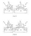
- FIG. 2illustrates SC transistor 16 and LC transistor 18 after the performance of conventional patterning and etching steps.
- SC transistor 16is etched to define a first gate stack 34 having a channel length (indicated in FIG. 2 by arrow 33 ) less than a predetermined length (L) and is consequently referred to herein as a short channel (SC) gate stack.
- LC transistor 18is etched to define a second gate stack 36 that has a channel length (indicated in FIG. 2 by arrow 35 ) equal to or greater than the predetermined length (L) and is consequently referred to herein as a long channel (LC) gate stack.
- the predetermined length (L)may have an exemplary value of approximately 0.1 ⁇ m.
- SC gate stack 34comprises a polycrystalline silicon layer 38 formed from polycrystalline silicon layer 32 ( FIG. 1 ), a metal gate 40 formed from metal gate layer 30 ( FIG. 1 ), and a gate insulator 42 formed from gate insulator layer 28 ( FIG. 1 ).
- LC gate stack 36likewise comprises a polycrystalline silicon layer 44 formed from polycrystalline silicon layer 32 ( FIG. 1 ), a metal gate 46 formed from metal gate layer 30 ( FIG. 1 ), and a gate insulator 48 formed from gate insulator layer 28 ( FIG. 1 ).
- SC gate stack 34serves as a permanent gate stack within SC transistor 16.
- a portion of LC gate stack 36, namely polycrystalline silicon layer 44 and metal gate 46is replaced during processing. For this reason, polycrystalline silicon layer 44 and metal gate 46 may be collectively referred to as the "LC dummy gate" herein below.
- SC transistor 16is separated from LC transistor 18 by a non-illustrated portion of the integrated circuit.
- an electrically-isolating elementis formed within this non-illustrated portion between SC transistor 16 and LC transistor 18.
- Any suitable processcan be utilized to form the electrically-isolating element; e.g., a conventional shallow trench isolation process can be employed wherein a shallow trench is etched into substrate 20, a thermal oxide liner is grown in the shallow trench, and an oxide is deposited into the trench and over the thermal oxide liner.
- FIG. 3illustrates SC transistor 16 and LC transistor 18 after the formation of source drain regions 54, 56 and sidewall spacers 62 near SC gate stack 34 and source drain regions 58, 60 and sidewall spacers 64 near LC gate stack 36.
- source 54 and drain 56selected ions are implanted into substrate 20 proximate SC gate stack 34, which serves as an ion implantation mask.
- source 58 and drain 60selected ions are implanted into substrates 20 proximate LC gate stack 36, which also serves as a mask.
- boron ionscan be implanted for a P-type MOS transistor; however, the particular ions selected for implantation will be dependent upon the type of device being constructed (e.g., for an N-type MOS transistor arsenic or phosphorus ions may be implanted).
- an activation annealis performed to electrically activate the implanted ions and to repair any imperfections in the silicon lattice caused by the ion implantation process.
- Spacers 62 and sidewall spacers 64are formed adjacent opposing sidewalls of SC gate stack 34 and LC gate stack 36, respectively.
- a spacer-forming materiale.g., SiO 2
- the spacer-forming materialcan be deposited to an exemplary thickness of approximately 15 nm utilizing LPCVD.
- the spacer-forming materialis then anisotropically etched utilizing, for example, a reactive ion etching (RIE) technique employing a CHF 3 , CF 4 , or SF 6 chemistry.
- RIEreactive ion etching
- the sidewall spacersmay be formed to include an underlying, relatively thin thermally grown oxide layer commonly referred to as a "zero spacer.”
- FIG. 3illustrates SC transistor 16 and LC transistor 18 as each including only a single set of sidewall spacers and a single source drain implantation.
- multiple spacers and multiple implantscan, and typically will, be utilized in the manufacture of SC transistor 16 and/or LC transistor 18.
- a second sidewall spacer formation step and a deeper implantation stepcan be performed.
- silicide layersare formed within the upper surfaces of the integrated circuit.
- a silicide layer 66is formed within source drain regions 54, 56, 58, 60;
- a silicide layer 68is formed within polycrystalline silicon layer 38 of SC gate stack 34; and, perhaps, a silicide layer 70 is formed within polycrystalline silicon layer 44 of LC gate stack 36.
- these layers of silicideare formed by depositing a layer of silicide-forming metal onto the surface of substrate 20 proximate source drain regions 54, 56, 58, and 60 and subsequently heating the silicide-forming metal utilizing, for example, rapid thermal annealing (RTA).
- RTArapid thermal annealing
- Preferred silicide-forming metalsinclude cobalt and nickel, although other silicide-forming metals may be employed (e.g., rhenium, ruthenium, palladium, etc.).
- the silicide-forming metalcan be deposited, for example, by sputtering to a thickness of approximately 5-30 nm. Any silicide-forming metal that is not in contact with exposed silicon (e.g., the silicide-forming metal that is deposited on sidewall spacers 62, 64 ) does not react during the RTA to form a silicide and can subsequently be removed via wet etching in a H 2 O 2 /H 2 SO 4 or HNO 3 /HCl solution.
- Silicide layers 66 and 68serve to increase conductivity and provide a convenient contact point. Silicide layer 70, if formed, is ultimately removed along with polycrystalline silicon layer 44 and metal gate 46 (i.e., dummy gate 50 labeled in FIG. 2 ) as described below in conjunction with FIGs. 11 and 12 .
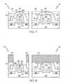
- FIG. 5illustrates the exemplary integrated circuit after a layer of etch stop material 72 has been deposited over substrate 20, SC transistor 16, and LC transistor 18.
- the layer of etch stop material 72comprises silicon nitride deposited to a thickness of approximately 50 nanometers utilizing, for example, CVD.
- the deposition of etch stop material 72 over SC gate stack 34 and sidewall spacers 62results in the production of a first raised etch stop feature 74 above SC transistor 16, and the deposition of etch stop material 72 over LC gate stack 36 and sidewall spacers 64 results in the production of a second raised etch stop feature 76 above LC transistor 18.
- an interlayer dielectric (ILD) 75is next deposited (e.g., via CVD) over the layer of etch stop material 72 (source drain regions 54, 56, 58, 60 are not shown in FIG. 6 , or any of the subsequent figures, for clarity).
- ILD 75can be deposited from, for example, a TEOS (tetra-ethyl orthosilicate) source.
- ILD 75is preferably deposited to a thickness sufficient to completely cover raised features 74 and 76 of etch stop layer 72.
- the upper surface of ILD 75is preferably planarized utilizing, for example, a chemical mechanical polishing or planarization (CMP) process. For example, and as shown in FIG.
- CMPchemical mechanical polishing or planarization
- the upper surface of ILD 75may be planarized beyond the apexes of raised etch stop features 74 and 76 to expose an upper portion of raised etch stop feature 74 and an upper portion of raised etch stop feature 76.
- the planarizationmay be discontinued prior to exposing raised etch stop features 74 and 76.
- the upper surface of ILD 75may reside at a level slightly above raised etch stop features 74 and 76 after planarization as indicated in FIG. 7 by dashed line 82. Etching can then be performed to expose the upper portions of raised etch stop features 74 and 76.
- a photoresist mask 84is placed over the upper surface of the integrated circuit and subsequently patterned. After patterning, photoresist mask 84 covers LC transistor 18 and any N-type devices included in the integrated circuit. Areas of the integrated circuit exposed through patterned mask 84 are then etched to produce an opening 86 in ILD 75 through which SC gate stack 34 and sidewall spacers 62 are exposed. The depth of the etch is preferably controlled such that the lower extremity of opening 86 is located below the upper surface of polycrystalline silicon layer 38. Stated differently, the etch is preferably performed to a depth sufficient to expose an upper portion of a sidewall 88 of polycrystalline silicon layer 38. In one specific exemplary embodiment, the etch depth is between approximately 200 to approximately 300 Angstrom.
- FIG. 9illustrates an optional oxidizing step that can be performed after removing photoresist mask 84 ( FIG. 8 ).
- the oxidizing stepassumes the form of an oxygen annealing process wherein the exposed portions of sidewall spacers 62 are introduced to an oxygen ambient (e.g., approximately 5-10 parts per million O 2 ) at a predetermined temperature (e.g., approximately 400-600 degrees Celsius) for a predetermined time period (e.g., up to 30 minutes or more).
- oxygen ambiente.g., approximately 5-10 parts per million O 2
- a predetermined temperaturee.g., approximately 400-600 degrees Celsius
- a predetermined time periode.g., up to 30 minutes or more.
- oxygen moleculesdiffuse downward through sidewall spacers 62 and into gate insulator 42 to fill oxygen vacancies within insulator 42 as described in more detail below.
- the oxygen moleculescannot easily diffuse through etch stop layer 72; thus, oxygen annealing has little to no effect on gate insulator 48 of
- a pre-oxidizing function 92 and a post-oxidizing function 90As may be appreciated by comparing function 92 to function 90, the oxidation of the gate insulator shifts the drain current-versus-gate voltage function to the left thus permitting a band edge voltage threshold to be achieved for a given drain current. This, in turn, permits SC transistor 16 to conduct more current at the same gate voltage.
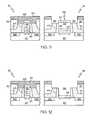
- a damascene processis utilized to replace silicide layer 70, polycrystalline silicon layer 44, and metal gate 46 (again, collectively referred to as the dummy gate) with a permanent metal gate.
- a photoresist mask 94is first placed over the integrated circuit to cover SC transistor 16 and any N-channel devices that may be included in the integrated circuit.
- An etching processis then performed to remove the exposed upper portion of raised etch stop feature 76 (labeled in FIGs. 5-7 ), an upper portion of sidewall spacers 64, and a surrounding portion of ILD 75.
- This etching stepcan be substantially identical to the etching step performed to expose SC gate stack 34 as described above in conjunction with FIG. 8 .
- the etching processforms an opening 95 within the upper surface of the integrated circuit over LC transistor 18 thus exposing an upper portion of LC gate stack 36 and sidewall spacers 64.
- a second etching stepis performed to remove silicide layer 70 and polycrystalline silicon layer 44 of LC gate stack 36. While photoresist mask 94 remains over SC transistor 16, an etchant selective to polycrystalline silicon (e.g., tetra-methyl ammonium hydroxide or TMAH) is applied to at least the exposed portion of LC gate stack 36. After polycrystalline silicon layer 44 has been adequately removed, a third etching step may be performed to remove metal gate 46 or a treatment step (e.g., alloying, oxygen annealing, fluorine implanting, etc.) may be used to modify the work function of LC gate stack 36.
- a treatment stepe.g., alloying, oxygen annealing, fluorine implanting, etc.
- metal gate 46comprises titanium nitride
- an ammonium hydroxide or peroxide-based chemistrycan be utilized to remove gate 46.
- FIG. 13illustrates SC transistor 16 and LC transistor 18 after the deposition of a metal film layer 98 over the integrated circuit and into LC device trench 96.
- photoresist mask 94is removed and, in a preferred embodiment, a relatively thin layer of a work function-setting metal (e.g., iridium, platinum, aluminum, ruthenium, etc.) is deposited (not shown).
- a work function-setting metale.g., iridium, platinum, aluminum, ruthenium, etc.
- Deposition of the work function-setting metal and metal film layer 98can be accomplished utilizing, for example, either a conventional electroless or a electrolytic deposition plating process.
- metal film layer 98comprises a metal having an effective work function of approximately 4.7 to approximately 5.1 electron volts.
- thermally unstable metalsexamples include iridium, platinum, palladium, and ruthenium.
- film material layer 98is then polished (e.g., via CMP) to produce a substantially planar surface.
- FIG. 14illustrates the integrated circuit after polishing. As shown in FIG. 14 , polishing results in the production of a cap 100 surrounding and contacting SC gate state 34 and in the production of a permanent LC gate 102 filling trench 96 (labeled in FIGs. 12 and 13 ) and contacting gate insulator 48.
- Additional stepsare performed to complete processing of the integrated circuit (e.g., the deposition of a second interlayer dielectric, further etching steps to provide vias to the source and drain regions, deposition of metal plugs, etc); however, such steps are well-known in the industry and are not described herein in the interests of concision.
- dummy gate replacementis described as being performed solely for a PFET long channel device (and not for a NFET long channel device); this example notwithstanding, it should be appreciated that dummy gate replacement may be performed for both PFET long channel devices and NFET long channel devices in alternative embodiments.
Landscapes
- Engineering & Computer Science (AREA)
- Physics & Mathematics (AREA)
- Condensed Matter Physics & Semiconductors (AREA)
- General Physics & Mathematics (AREA)
- Manufacturing & Machinery (AREA)
- Computer Hardware Design (AREA)
- Microelectronics & Electronic Packaging (AREA)
- Power Engineering (AREA)
- Insulated Gate Type Field-Effect Transistor (AREA)
- Metal-Oxide And Bipolar Metal-Oxide Semiconductor Integrated Circuits (AREA)
- Electrodes Of Semiconductors (AREA)
- Thin Film Transistor (AREA)
Abstract
Description
- The present invention relates generally to an integrated circuit and, more particularly, to a method for making an integrated circuit having both long and short channel metal gate devices.
- The majority of present day integrated circuits (ICs) are implemented utilizing a plurality of interconnected field effect transistors (FETs), also referred to as metal oxide semiconductor field effect transistors (MOSFETs) or simply MOS transistors. A MOS transistor includes a gate electrode, which serves as a control electrode, and source and drain electrodes. A channel extends between the source and drain electrodes. Current flows through this channel upon application of a voltage (referred to as the "threshold voltage" or Vt) to the gate electrode sufficient to form an inversion region in the transistor substrate.
- The document
US2006/0102962 discloses a method for manufacturing an integrated circuit comprising a first gate electrode and a second gate electrode, the area of the second gate electrode being larger than that of the first gate electrode. - The document
US2005/0186747 discloses CMOS silicide metal gate integration comprising an etch back process such that a dielectric layer and a dielectric cap are selectively removed. - For MOS transistors employing metal gate stacks and high-k dielectrics, it is desirable that the target Vt (referred to herein as the "bandedge Vt") corresponds to within 100 millivolts of the conduction band or valence band edge whether the device is NMOS or PMOS. It has, however, proven difficult to construct a metal gate MOS transistor having a bandedge Vt for several reasons. Fixed positive charges due to oxygen vacancies present in the high-k material may shift the transistor's threshold voltage away from the desired bandedge Vt. Furthermore, metals having work functions that yield bandedge threshold voltages (e.g., work functions of approximately 4.7-5.1 electron volts) are typically thermally unstable at temperatures exceeding 400 degrees Celsius. Such thermally unstable metals are generally unable to withstand the high temperatures experienced during source-drain activation annealing. For this reason, a gate-last approach is typically employed to construct MOS transistors including metal gates formed from thermally unstable metals. For example, a damascene process may be employed wherein a dummy gate is initially installed and subsequently removed via etching to produce a trench. A thermally unstable metal may then be deposited into the trench and polished to define a permanent metal gate.
- While being generally well-suited for use in conjunction with long channel (LC) transistors (e.g., devices wherein the channel length exceeds a predetermined value, which may be, for example, approximately 0.1 µm), the above-described damascene process has certain disadvantages when utilized in conjunction with short channel (SC) transistors (e.g., devices wherein the channel length is equal to or less than the predetermined value). For example, due to the small size of the device, the entire dummy gate may not be removed during the etching process. Furthermore, when deposited over the open trench of an SC transistor, the metal gate material may pinch-off near the mouth of the trench before the trench is completely filled. Voiding can consequently occur within the body of the trench. Thus, for an IC including SC transistors and LC transistors, the damascene process is generally unacceptable and an etching process is generally utilized to construct the metal gates for both types of transistors thus generally preventing the use of thermally unstable metals in LC transistors to achieve bandedge voltage thresholds.
- Accordingly, it would be desirable to provide a method for manufacturing a MOS transistor having short channel devices and long channel devices that permits bandedge voltage thresholds to be achieved for both the short and long channel devices. In particular, it would be desirable for such a method to permit thermally unstable metals to be utilized in the fabrication of the long channel devices, while also permitting oxygen vacancies present in the short channel devices to be repaired. Furthermore, other desirable features and characteristics of the present invention will become apparent from the subsequent detailed description and the appended claims, taken in conjunction with the accompanying drawings and the foregoing technical field and background.
- A method for manufacturing an integrated circuit is provided as recited in claim 1.
- A method is provided for manufacturing an integrated circuit including a short channel (SC) device and a long channel (LC) device each overlaid by an interlayer dielectric. The SC device has an SC gate stack and the LC device initially has a dummy gate. In one embodiment, the method includes the steps of removing the dummy gate to form an LC device trench, and depositing metal gate material over the SC device and the LC device. The metal gate material contacts the SC gate stack and substantially fills the LC device trench.
- In accordance with another embodiment, an integrated circuit is provided that includes a substrate, a short channel (SC) device, a long channel (LC) device, an etch stop layer deposited over an upper surface of the substrate, and an interlayer dielectric deposited over an upper surface of the etch stop layer. The SC device and the LC device each include a source formed in the substrate, a drain formed in the substrate and spaced apart from the source, and a channel formed in the substrate between the source and drain. The SC device further includes an SC gate stack, which, in turn, includes an SC gate insulator disposed above the channel, an SC metal gate disposed above the gate insulator, a polycrystalline silicon layer disposed above the metal gate, and a silicide layer disposed above the polycrystalline silicon layer. The LC device further includes an LC gate insulator disposed above the channel, and an LC metal gate contacting the gate insulator. An SC cap is disposed in the interlayer dielectric and contacts the SC gate stack. The SC gate stack and the LC metal gate extend through the etch stop layer, and the SC cap and the LC metal gate are exposed through the upper surface of the interlayer dielectric.
- In accordance with another embodiment not forming part of the invention, an integrated circuit is provided that includes a substrate, a short channel (SC) device, a long channel (LC) device, an etch stop deposited over an upper surface of the substrate, and an interlayer dielectric deposited over an upper surface of the etch stop layer. The SC device includes an SC gate insulator disposed above a first portion of the substrate, an SC metal gate disposed above the gate insulator, a polycrystalline silicon layer disposed above the metal gate, and a silicide layer formed on the polycrystalline silicon layer. The LC device includes an LC gate insulator disposed above a second portion of the substrate, and an LC metal gate overlying the gate insulator. An SC cap is disposed in the interlayer dielectric, contacts the SC gate stack, and is substantially formed from the same metal as is the LC metal gate.
- The present invention will hereinafter be described in conjunction with the following drawing figures, wherein like numerals denote like elements, and wherein:
FIGs. 1-9 are simplified cross-sectional views illustrating a first group of steps performed during an exemplary device manufacturing process;FIG. 10 is a graph illustrating the effect of the exemplary annealing step illustrated inFIG. 9 on the short channel device threshold voltage; andFIGs. 11-14 are simplified cross-sectional views illustrating a second group of steps performed during the exemplary device manufacturing process.- The following detailed description is merely exemplary in nature and is not intended to limit the invention or the application and uses of the invention. Furthermore, there is no intention to be bound by any expressed or implied theory presented in the preceding technical field, background, brief summary or the following detailed description. Although the term "MOS device" properly refers to a device having a metal gate electrode and an oxide gate insulator, that term will be used throughout to refer to any semiconductor device that includes a conductive gate electrode that is positioned over a gate insulator (whether oxide or other insulator) which, in turn, is positioned over a semiconductor substrate.
- An exemplary method for the manufacture of an integrated circuit having a P-type short channel (SC) transistor and a P-type long channel (LC) transistor will be described below in conjunction with
FIGs. 1-14 . However, it is emphasized that alternative embodiments of the inventive method can be utilized to construct an integrated circuit including other types of SC and LC devices. For example, similar method steps are suitable for use in the manufacture of an N-type MOS device with appropriate changes in dopant types. Likewise, similar method steps can used to manufacture complementary MOS transistors (CMOS). Furthermore, various steps in the manufacture of MOS transistors are well-known and, in the interests of brevity, will only be mentioned briefly herein or will be omitted entirely without providing the well-known process details. FIGs. 1-9 and11-14 are simplified cross-sectional views illustrating various steps of an exemplary method for manufacturing an integrated circuit including a short channel (SC) device and a long channel (LC) device. For the purposes of the present description, a "short channel device" is defined as a device having a channel length less than a predetermined length (L). Conversely, a "long channel device" is defined as a device having a channel length equal to or greater than the predetermined length (L). The value of the predetermined length (L) will inevitably vary amongst different embodiments; however, as a non-limiting example, the predetermined length (L) may have a value of approximately 0.1 micrometer (µm).- Referring initially to
FIG. 1 , the exemplary method of manufacture commences with the step of providing asemiconductor substrate 20 on which anLC transistor 16 and aSC transistor 18 will be constructed.Semiconductor substrate 20 is preferably a silicon substrate (the term "silicon substrate" is used herein to encompass the relatively pure silicon materials typically used in the semiconductor industry as well as silicon admixed with other elements, such as germanium and the like).Silicon substrate 20 can be a bulk silicon wafer. Alternatively, and as shown inFIG. 1 ,silicon substrate 20 can comprise a thin layer ofsilicon 22 on an insulating layer24 (commonly know as a "silicon-on-insulator wafer" or "SOI wafer") that is, in turn, supported by asilicon carrier wafer 26. - A
gate insulator layer 28 is formed on the upper surface ofsilicon substrate 22.Gate insulator layer 28 may be a thermally grown silicon dioxide formed by heating the silicon substrate in an oxidizing ambient; however, it is preferred thatgate insulator layer 28 is formed by the deposition of a high-k dielectric material, such as HfSiO, HfO2, ZrO2, or any other standard high-k dielectric. Any suitable deposition technique may be utilized to formgate insulator layer 28, such as chemical vapor deposition (CVD), low pressure chemical vapor deposition (LPCVD), and plasma enhanced chemical vapor deposition (PECVD).Gate insulator layer 28 is preferably deposited to a thickness less than approximately 5 nanometers (nm) and ideally to a thickness less than approximately 3 nm. - Referring still to
FIG. 1 , ametal gate layer 30 is deposited ongate insulator layer 28 utilizing a conventional deposition technique. The metal deposited to formmetal gate layer 30 will be chosen, in part, to yield a desired threshold voltage (Vt) forSC transistor 16, although it will be appreciated that other factors (e.g., the oxidation process described below) will also affect the final Vt ofSC transistor 16. A non-exhaustive list of metals suitable for use in the formation ofmetal gate layer 30 includes TiN, TaN, HfSi, and TaC.Metal gate layer 30 is preferably deposited to a thickness of approximately 2-10 nm. - In the illustrated exemplary embodiment, a layer of
polycrystalline silicon 32 is deposited onto the upper surface ofmetal gate layer 30.Polycrystalline silicon layer 32 is preferably deposited as undoped polycrystalline silicon that is subsequently impurity doped by ion implantation, although the polycrystalline silicon may also be doped in situ. In one implementation,polycrystalline silicon layer 32 is deposited utilizing LPCVD and the hydrogen reduction of silane.Polycrystalline silicon layer 32 is preferably deposited to a thickness of approximately 50-100 nm. FIG. 2 illustratesSC transistor 16 andLC transistor 18 after the performance of conventional patterning and etching steps.SC transistor 16 is etched to define afirst gate stack 34 having a channel length (indicated inFIG. 2 by arrow33) less than a predetermined length (L) and is consequently referred to herein as a short channel (SC) gate stack. Similarly,LC transistor 18 is etched to define asecond gate stack 36 that has a channel length (indicated inFIG. 2 by arrow35) equal to or greater than the predetermined length (L) and is consequently referred to herein as a long channel (LC) gate stack. As previously stated, the predetermined length (L) may have an exemplary value of approximately 0.1 µm.SC gate stack 34 comprises apolycrystalline silicon layer 38 formed from polycrystalline silicon layer 32 (FIG. 1 ), ametal gate 40 formed from metal gate layer30 (FIG. 1 ), and agate insulator 42 formed from gate insulator layer28 (FIG. 1 ).LC gate stack 36 likewise comprises apolycrystalline silicon layer 44 formed from polycrystalline silicon layer32 (FIG. 1 ), ametal gate 46 formed from metal gate layer30 (FIG. 1 ), and agate insulator 48 formed from gate insulator layer28 (FIG. 1 ). As will be described in detail below,SC gate stack 34 serves as a permanent gate stack withinSC transistor 16. In contrast, a portion ofLC gate stack 36, namelypolycrystalline silicon layer 44 andmetal gate 46, is replaced during processing. For this reason,polycrystalline silicon layer 44 andmetal gate 46 may be collectively referred to as the "LC dummy gate" herein below.- As indicated in
FIG. 2 byarrow 52,SC transistor 16 is separated fromLC transistor 18 by a non-illustrated portion of the integrated circuit. Although not shown inFIG. 2 , it will be appreciated by one of ordinary skill in the art that an electrically-isolating element is formed within this non-illustrated portion betweenSC transistor 16 andLC transistor 18. Any suitable process can be utilized to form the electrically-isolating element; e.g., a conventional shallow trench isolation process can be employed wherein a shallow trench is etched intosubstrate 20, a thermal oxide liner is grown in the shallow trench, and an oxide is deposited into the trench and over the thermal oxide liner. FIG. 3 illustratesSC transistor 16 andLC transistor 18 after the formation ofsource drain regions sidewall spacers 62 nearSC gate stack 34 andsource drain regions sidewall spacers 64 nearLC gate stack 36. To createsource 54 anddrain 56, selected ions are implanted intosubstrate 20 proximateSC gate stack 34, which serves as an ion implantation mask. Similarly, to formsource 58 anddrain 60, selected ions are implanted intosubstrates 20 proximateLC gate stack 36, which also serves as a mask. By way of example, boron ions can be implanted for a P-type MOS transistor; however, the particular ions selected for implantation will be dependent upon the type of device being constructed (e.g., for an N-type MOS transistor arsenic or phosphorus ions may be implanted). After ion implantation, an activation anneal is performed to electrically activate the implanted ions and to repair any imperfections in the silicon lattice caused by the ion implantation process.Sidewall spacers 62 andsidewall spacers 64 are formed adjacent opposing sidewalls ofSC gate stack 34 andLC gate stack 36, respectively. In accordance with one exemplary technique, a spacer-forming material (e.g., SiO2) is deposited oversubstrate 20,SC gate stack 34, andLC gate stack 36. The spacer-forming material can be deposited to an exemplary thickness of approximately 15 nm utilizing LPCVD. The spacer-forming material is then anisotropically etched utilizing, for example, a reactive ion etching (RIE) technique employing a CHF3, CF4, or SF6 chemistry. This results in the formation ofsidewall spacers 62 on opposing sidewalls ofSC gate stack 34 andsidewall spacers 64 on opposing sidewalls ofLC gate stack 36. Although not shown inFIG. 3 , the sidewall spacers may be formed to include an underlying, relatively thin thermally grown oxide layer commonly referred to as a "zero spacer."- For the purposes of clarity,
FIG. 3 illustratesSC transistor 16 andLC transistor 18 as each including only a single set of sidewall spacers and a single source drain implantation. This notwithstanding, it will be readily appreciated that multiple spacers and multiple implants can, and typically will, be utilized in the manufacture ofSC transistor 16 and/orLC transistor 18. For example, after the performance of the above-described sidewall spacer formation step and shallow implantation step, a second sidewall spacer formation step and a deeper implantation step can be performed. - Next, as shown in
FIG. 4 , silicide layers are formed within the upper surfaces of the integrated circuit. In particular, asilicide layer 66 is formed withinsource drain regions silicide layer 68 is formed withinpolycrystalline silicon layer 38 ofSC gate stack 34; and, perhaps, asilicide layer 70 is formed withinpolycrystalline silicon layer 44 ofLC gate stack 36. In one option, these layers of silicide are formed by depositing a layer of silicide-forming metal onto the surface ofsubstrate 20 proximatesource drain regions sidewall spacers 62, 64) does not react during the RTA to form a silicide and can subsequently be removed via wet etching in a H2O2/H2SO4 or HNO3/HCl solution. Silicide layers66 and68 serve to increase conductivity and provide a convenient contact point.Silicide layer 70, if formed, is ultimately removed along withpolycrystalline silicon layer 44 and metal gate46 (i.e.,dummy gate 50 labeled inFIG. 2 ) as described below in conjunction withFIGs. 11 and 12 . FIG. 5 illustrates the exemplary integrated circuit after a layer ofetch stop material 72 has been deposited oversubstrate 20,SC transistor 16, andLC transistor 18. In a preferred embodiment, the layer ofetch stop material 72 comprises silicon nitride deposited to a thickness of approximately 50 nanometers utilizing, for example, CVD. The deposition ofetch stop material 72 overSC gate stack 34 andsidewall spacers 62 results in the production of a first raisedetch stop feature 74 aboveSC transistor 16, and the deposition ofetch stop material 72 overLC gate stack 36 andsidewall spacers 64 results in the production of a second raisedetch stop feature 76 aboveLC transistor 18.- With reference to
FIG. 6 , an interlayer dielectric (ILD)75 is next deposited (e.g., via CVD) over the layer of etch stop material72 (source drain regions FIG. 6 , or any of the subsequent figures, for clarity).ILD 75 can be deposited from, for example, a TEOS (tetra-ethyl orthosilicate) source.ILD 75 is preferably deposited to a thickness sufficient to completely cover raised features74 and76 ofetch stop layer 72. The upper surface ofILD 75 is preferably planarized utilizing, for example, a chemical mechanical polishing or planarization (CMP) process. For example, and as shown inFIG. 7 , the upper surface ofILD 75 may be planarized beyond the apexes of raised etch stop features74 and76 to expose an upper portion of raisedetch stop feature 74 and an upper portion of raisedetch stop feature 76. Alternatively, the planarization may be discontinued prior to exposing raised etch stop features74 and76. In this latter case, the upper surface ofILD 75 may reside at a level slightly above raised etch stop features74 and76 after planarization as indicated inFIG. 7 by dashedline 82. Etching can then be performed to expose the upper portions of raised etch stop features74 and76. - Turning now to
FIG. 8 , aphotoresist mask 84 is placed over the upper surface of the integrated circuit and subsequently patterned. After patterning,photoresist mask 84 coversLC transistor 18 and any N-type devices included in the integrated circuit. Areas of the integrated circuit exposed through patternedmask 84 are then etched to produce anopening 86 inILD 75 through whichSC gate stack 34 andsidewall spacers 62 are exposed. The depth of the etch is preferably controlled such that the lower extremity of opening86 is located below the upper surface ofpolycrystalline silicon layer 38. Stated differently, the etch is preferably performed to a depth sufficient to expose an upper portion of asidewall 88 ofpolycrystalline silicon layer 38. In one specific exemplary embodiment, the etch depth is between approximately 200 to approximately 300 Angstrom. FIG. 9 illustrates an optional oxidizing step that can be performed after removing photoresist mask84 (FIG. 8 ). In a preferred embodiment, the oxidizing step assumes the form of an oxygen annealing process wherein the exposed portions ofsidewall spacers 62 are introduced to an oxygen ambient (e.g., approximately 5-10 parts per million O2) at a predetermined temperature (e.g., approximately 400-600 degrees Celsius) for a predetermined time period (e.g., up to 30 minutes or more). During this oxygen annealing process, oxygen molecules diffuse downward throughsidewall spacers 62 and intogate insulator 42 to fill oxygen vacancies withininsulator 42 as described in more detail below. Notably, the oxygen molecules cannot easily diffuse throughetch stop layer 72; thus, oxygen annealing has little to no effect ongate insulator 48 ofLC transistor 18.- As previously explained, it has been discovered that positive fixed charges produced by oxygen vacancies within the gate insulator (e.g., gate insulator42) may shift the threshold voltage (Vt) of a SC device away from the desired bandedge (BE) V1. The oxidizing step illustrated in
FIG. 9 significantly reduces or entirely eliminates these fixed charges by filling the oxygen vacancies ingate insulator 42, which permits the actual threshold voltage ofSC transistor 16 to approach the desired BE Vt. This concept is graphically illustrated inFIG. 10 wherein drain current (Id) is plotted along the horizontal axis and gate voltage (Vg) is plotted along the vertical axis. Two functions are illustrated inFIG. 10 , namely, apre-oxidizing function 92 and apost-oxidizing function 90. As may be appreciated by comparingfunction 92 to function90, the oxidation of the gate insulator shifts the drain current-versus-gate voltage function to the left thus permitting a band edge voltage threshold to be achieved for a given drain current. This, in turn, permitsSC transistor 16 to conduct more current at the same gate voltage.. - After the performance of the above-described oxidization process, a damascene process is utilized to replace
silicide layer 70,polycrystalline silicon layer 44, and metal gate46 (again, collectively referred to as the dummy gate) with a permanent metal gate. With reference toFIG. 11 , aphotoresist mask 94 is first placed over the integrated circuit to coverSC transistor 16 and any N-channel devices that may be included in the integrated circuit. An etching process is then performed to remove the exposed upper portion of raised etch stop feature76 (labeled inFIGs. 5-7 ), an upper portion ofsidewall spacers 64, and a surrounding portion ofILD 75. This etching step can be substantially identical to the etching step performed to exposeSC gate stack 34 as described above in conjunction withFIG. 8 . The etching process forms anopening 95 within the upper surface of the integrated circuit overLC transistor 18 thus exposing an upper portion ofLC gate stack 36 andsidewall spacers 64. - Next, and as shown in
FIG. 12 , a second etching step is performed to removesilicide layer 70 andpolycrystalline silicon layer 44 ofLC gate stack 36. Whilephotoresist mask 94 remains overSC transistor 16, an etchant selective to polycrystalline silicon (e.g., tetra-methyl ammonium hydroxide or TMAH) is applied to at least the exposed portion ofLC gate stack 36. Afterpolycrystalline silicon layer 44 has been adequately removed, a third etching step may be performed to removemetal gate 46 or a treatment step (e.g., alloying, oxygen annealing, fluorine implanting, etc.) may be used to modify the work function ofLC gate stack 36. The particular etchant employed will, of course, depend upon the metal used to formmetal gate 46. If, for example,metal gate 46 comprises titanium nitride, an ammonium hydroxide or peroxide-based chemistry can be utilized to removegate 46. Thus, through the series of etching steps illustrated inFIG. 12 , the components of dummy gate50 (i.e.,polycrystalline silicon layer 44 andmetal gate 46 as labeled inFIG. 2 ) are removed to form anLC device trench 96 betweensidewall spacers 64. FIG. 13 illustratesSC transistor 16 andLC transistor 18 after the deposition of ametal film layer 98 over the integrated circuit and intoLC device trench 96. Before the deposition ofmetal film layer 98,photoresist mask 94 is removed and, in a preferred embodiment, a relatively thin layer of a work function-setting metal (e.g., iridium, platinum, aluminum, ruthenium, etc.) is deposited (not shown). Deposition of the work function-setting metal andmetal film layer 98 can be accomplished utilizing, for example, either a conventional electroless or a electrolytic deposition plating process. In a preferred embodiment,metal film layer 98 comprises a metal having an effective work function of approximately 4.7 to approximately 5.1 electron volts. As explained above, metals having work functions falling within this idealized range tend to be unstable at temperatures exceeding 400 degrees Celsius and are consequently referred to herein as thermally unstable metals. Examples of suitable thermally unstable metals include iridium, platinum, palladium, and ruthenium. After being deposited to a sufficient thickness and substantially fillingtrench 96,film material layer 98 is then polished (e.g., via CMP) to produce a substantially planar surface.FIG. 14 illustrates the integrated circuit after polishing. As shown inFIG. 14 , polishing results in the production of acap 100 surrounding and contactingSC gate state 34 and in the production of apermanent LC gate 102 filling trench96 (labeled inFIGs. 12 and13 ) and contactinggate insulator 48. Additional steps are performed to complete processing of the integrated circuit (e.g., the deposition of a second interlayer dielectric, further etching steps to provide vias to the source and drain regions, deposition of metal plugs, etc); however, such steps are well-known in the industry and are not described herein in the interests of concision.- It should thus be appreciated that there has been provided an example of a method suitable for manufacturing an integrated circuit having both short and long channel devices. The damascene-type replacement gate process described above enables thermally unstable metals to be employed in the construction of long channel devices thus enabling bandedge threshold voltages to be achieved for long channel devices. In addition, the exemplary method repairs oxygen vacancies that may occur within the short channel PFET devices thereby further permitting bandedge threshold voltages to be achieved for short channel devices. In the above-described exemplary embodiment, dummy gate replacement is described as being performed solely for a PFET long channel device (and not for a NFET long channel device); this example notwithstanding, it should be appreciated that dummy gate replacement may be performed for both PFET long channel devices and NFET long channel devices in alternative embodiments.
- While at least one exemplary embodiment has been presented in the foregoing detailed description, it should be appreciated that a vast number of variations exist. It should also be appreciated that the exemplary embodiment or exemplary embodiments are only examples, and are not intended to limit the scope, applicability, or configuration of the invention in any way. Rather, the foregoing detailed description will provide those skilled in the art with a convenient road map for implementing the exemplary embodiment or exemplary embodiments. Although certain embodiments of the method described above include a thin seed layer and a deposited metal layer, after subsequent heating steps that may take place during further processing the seed layer and the deposited metal layer may merge together so that a separate and distinct seed layer is not discernable. It should be understood that various changes can be made in the function and arrangement of elements without departing from the scope of the invention as set forth in the appended claims.
Claims (9)
- A method tor manufacturing an integrated circuit including a short channel (SC) device (16) having a channel length less than a predetermined length and a long channel (LC) device (18) having a channel length greater than or equal to the predetermined length, the SC device (16) and the LC device (18) each overlaid by an interlayer dielectric (75), the SC device (16) having an SC gate stack (34) and the LC device (18) initially having a dummy gate (50), the method comprising:removing the dummy gate (50) to form an LC device trench (96),depositing metal gate material (98) over the SC device (16) and the LC device (18), the metal gate material (98) contacting the SC gate stack (34) and substantially filling the LC device trench (96);characterized by:covering the LC device (16) with a photoresist mask (84); andetching a selected portion of the interlayer dielectric (75) such that the SC gate stack (34) is exposed through the interlayer dielectric (75) while the dummy gate (50) remains covered by the interlayer dielectric (75).
- A method according to Claim 1 further comprising the step of oxidizing the SC gate stack (34) after etching the selected portion of the interlayer dielectric (75).
- A method according to Claim 2 wherein the SC device (16) includes a sidewall spacer (62) adjacent the SC gate stack (34), wherein the SC gate stack (34) includes a gate insulator (42), and wherein the step of oxidizing comprises annealing the gate insulator (42) white exposing the sidewall spacer (62) to an oxygen ambient.
- A method according to Claim 1 wherein the SC device (16) and the LC device (18) are each devices, wherein the integrated circuit further includes an N-typc device, and wherein the step of covering comprises placing a photoresist mask (84) on the integrated circuit covering the LC device (18) and the N-type device.
- A method according to Claim 1 wherein the SC device (16) and the LC device (18) are each P-type devices, wherein the integrated circuit further includes an N-type device, and wherein the step of removing comprises: covering the SC device (16) and the device with a photoresist mask (84); and etching the dummy gate (50).
- A method according to Claim Further comprising: forming an etch stop layer (72) over a portion of the integrated circuit including the SC gate stack (34) and the dummy gate (50) such that the etch stop layer (72) includes a first raised etch stop feature (74) above the SC gate stack (34) and a second raised etch stop feature (76) above the dummy gate (50): and depositing the interlayer dielectric (75) over the etch stop layer (72) to cover the first raised etch stop feature (74) and the second raised etch stop feature (76).
- A method according to Claim 1 wherein the SC gate stack (34) includes a polycrystalline silicon layer (38) having a sidewall (88), and wherein the step of etching comprises creating an opening (86) surrounding SC gate stack (34) and exposing at least a portion of the sidewall (88).
- A method according to Claim 7 wherein the step of depositing comprises substantially filling the opening (86) with the metal gate material (98).
- A method according to Claim 1 wherein the metal gate material (98) comprises a metal having an effective work function of approximately 4.7 to approximately 5.1 electron volts.
Applications Claiming Priority (2)
| Application Number | Priority Date | Filing Date | Title |
|---|---|---|---|
| US12/048,414US7723192B2 (en) | 2008-03-14 | 2008-03-14 | Integrated circuit long and short channel metal gate devices and method of manufacture |
| PCT/US2009/001617WO2009114187A1 (en) | 2008-03-14 | 2009-03-13 | Integrated circuit having long and short channel metal gate devices and method of manufacture |
Publications (2)
| Publication Number | Publication Date |
|---|---|
| EP2257977A1 EP2257977A1 (en) | 2010-12-08 |
| EP2257977B1true EP2257977B1 (en) | 2012-08-08 |
Family
ID=40756373
Family Applications (1)
| Application Number | Title | Priority Date | Filing Date |
|---|---|---|---|
| EP09718840AActiveEP2257977B1 (en) | 2008-03-14 | 2009-03-13 | Method for manufacturing an integrated circuit having long and short channel metal gate devices |
Country Status (7)
| Country | Link |
|---|---|
| US (2) | US7723192B2 (en) |
| EP (1) | EP2257977B1 (en) |
| JP (2) | JP5466181B2 (en) |
| KR (1) | KR101454457B1 (en) |
| CN (1) | CN101971323B (en) |
| TW (1) | TWI474440B (en) |
| WO (1) | WO2009114187A1 (en) |
Families Citing this family (35)
| Publication number | Priority date | Publication date | Assignee | Title |
|---|---|---|---|---|
| US8860174B2 (en) | 2006-05-11 | 2014-10-14 | Micron Technology, Inc. | Recessed antifuse structures and methods of making the same |
| US20070262395A1 (en) | 2006-05-11 | 2007-11-15 | Gibbons Jasper S | Memory cell access devices and methods of making the same |
| US8008144B2 (en) | 2006-05-11 | 2011-08-30 | Micron Technology, Inc. | Dual work function recessed access device and methods of forming |
| US8097500B2 (en)* | 2008-01-14 | 2012-01-17 | International Business Machines Corporation | Method and apparatus for fabricating a high-performance band-edge complementary metal-oxide-semiconductor device |
| US7790553B2 (en)* | 2008-07-10 | 2010-09-07 | International Business Machines Corporation | Methods for forming high performance gates and structures thereof |
| US8105931B2 (en)* | 2008-08-27 | 2012-01-31 | Taiwan Semiconductor Manufacturing Company, Ltd. | Method of fabricating dual high-k metal gates for MOS devices |
| US7824986B2 (en)* | 2008-11-05 | 2010-11-02 | Micron Technology, Inc. | Methods of forming a plurality of transistor gates, and methods of forming a plurality of transistor gates having at least two different work functions |
| US8298882B2 (en)* | 2009-09-18 | 2012-10-30 | International Business Machines Corporation | Metal gate and high-K dielectric devices with PFET channel SiGe |
| US8093117B2 (en)* | 2010-01-14 | 2012-01-10 | Taiwan Semiconductor Manufacturing Company, Ltd. | Method of forming a metal gate |
| US8354313B2 (en)* | 2010-04-30 | 2013-01-15 | International Business Machines Corporation | Method to optimize work function in complementary metal oxide semiconductor (CMOS) structures |
| KR101815527B1 (en) | 2010-10-07 | 2018-01-05 | 삼성전자주식회사 | Semiconductor device and method for manufacturing the same |
| CN102456621A (en)* | 2010-10-29 | 2012-05-16 | 中芯国际集成电路制造(上海)有限公司 | Semiconductor device structure and method for manufacturing the same |
| CN102479693B (en)* | 2010-11-30 | 2013-11-06 | 中芯国际集成电路制造(北京)有限公司 | Gate forming method |
| CN102646589B (en)* | 2011-02-17 | 2015-01-07 | 中芯国际集成电路制造(上海)有限公司 | Manufacturing method of MOSFET (metal-oxide-semiconductor field effect transistor) |
| US8432002B2 (en)* | 2011-06-28 | 2013-04-30 | International Business Machines Corporation | Method and structure for low resistive source and drain regions in a replacement metal gate process flow |
| CN102983097B (en)* | 2011-09-05 | 2015-02-18 | 中芯国际集成电路制造(上海)有限公司 | Method for producing metal plug for metal gate |
| CN103094110B (en)* | 2011-10-31 | 2016-02-03 | 中芯国际集成电路制造(上海)有限公司 | Make the method for semiconductor device |
| US8936979B2 (en)* | 2012-06-11 | 2015-01-20 | GlobalFoundries, Inc. | Semiconductor devices having improved gate height uniformity and methods for fabricating same |
| US8946035B2 (en)* | 2012-09-27 | 2015-02-03 | Taiwan Semiconductor Manufacturing Co., Ltd. | Replacement channels for semiconductor devices and methods for forming the same using dopant concentration boost |
| US9059206B2 (en)* | 2012-12-10 | 2015-06-16 | International Business Machines Corporation | Epitaxial grown extremely shallow extension region |
| JP6026914B2 (en)* | 2013-02-12 | 2016-11-16 | ルネサスエレクトロニクス株式会社 | Manufacturing method of semiconductor device |
| US10038063B2 (en)* | 2014-06-10 | 2018-07-31 | International Business Machines Corporation | Tunable breakdown voltage RF FET devices |
| KR102230198B1 (en) | 2014-09-23 | 2021-03-19 | 삼성전자주식회사 | Semiconductor device and method for manufacturing the same |
| US9412667B2 (en) | 2014-11-25 | 2016-08-09 | International Business Machines Corporation | Asymmetric high-k dielectric for reducing gate induced drain leakage |
| US9425213B1 (en) | 2015-06-30 | 2016-08-23 | Stmicroelectronics, Inc. | Stacked short and long channel FinFETs |
| CN106531776B (en)* | 2015-09-11 | 2021-06-29 | 联华电子股份有限公司 | Semiconductor structure |
| US9779997B2 (en)* | 2015-12-31 | 2017-10-03 | Taiwan Semiconductor Manufacturing Co., Ltd. | Semiconductor device and a method for fabricating the same |
| US9716093B1 (en)* | 2016-03-07 | 2017-07-25 | Taiwan Semiconductor Manufacturing Co., Ltd. | Semiconductor device |
| US10043584B2 (en)* | 2016-10-28 | 2018-08-07 | International Business Machines Corporation | Three terminal fuse structure created by oxygen vacancy traps in hafnium-based oxides |
| US10043713B1 (en)* | 2017-05-10 | 2018-08-07 | Globalfoundries Inc. | Method to reduce FinFET short channel gate height |
| US10811528B2 (en) | 2018-03-21 | 2020-10-20 | International Business Machines Corporation | Two step fin etch and reveal for VTFETs and high breakdown LDVTFETs |
| US11152510B2 (en)* | 2018-07-25 | 2021-10-19 | International Business Machines Corporation | Long channel optimization for gate-all-around transistors |
| US12046475B2 (en)* | 2021-01-14 | 2024-07-23 | Taiwan Semiconductor Manufacturing Co., Ltd. | Surface oxidation control of metal gates using capping layer |
| EP4281822A4 (en) | 2021-01-19 | 2024-05-01 | O-Net Communications (USA) Inc. | Wavelength selective switch |
| US12349445B2 (en)* | 2022-01-25 | 2025-07-01 | International Business Machines Corporation | Vertically integrated semiconductor device |
Family Cites Families (22)
| Publication number | Priority date | Publication date | Assignee | Title |
|---|---|---|---|---|
| JPS6045053A (en)* | 1983-08-22 | 1985-03-11 | Mitsubishi Electric Corp | Semiconductor device |
| JPH11260934A (en)* | 1998-03-10 | 1999-09-24 | Matsushita Electric Ind Co Ltd | Semiconductor device and manufacturing method thereof |
| JP3023355B1 (en)* | 1998-12-25 | 2000-03-21 | 松下電器産業株式会社 | Semiconductor device and manufacturing method thereof |
| US6255698B1 (en)* | 1999-04-28 | 2001-07-03 | Advanced Micro Devices, Inc. | Separately optimized gate structures for n-channel and p-channel transistors in an integrated circuit |
| US6248675B1 (en)* | 1999-08-05 | 2001-06-19 | Advanced Micro Devices, Inc. | Fabrication of field effect transistors having dual gates with gate dielectrics of high dielectric constant using lowered temperatures |
| JP2001085677A (en)* | 1999-09-09 | 2001-03-30 | Mitsubishi Electric Corp | Method for manufacturing semiconductor device |
| KR100350056B1 (en)* | 2000-03-09 | 2002-08-24 | 삼성전자 주식회사 | Method of forming a self-aligned contact pad in a damascene gate process |
| US6607950B2 (en)* | 2000-03-30 | 2003-08-19 | Interuniversitair Microelektronic Centrum (Imec) | MIS transistors with a metal gate and high-k dielectric and method of forming |
| JP2002151666A (en)* | 2000-11-15 | 2002-05-24 | Mitsubishi Electric Corp | Method of manufacturing semiconductor device and semiconductor device |
| US6468851B1 (en) | 2002-01-02 | 2002-10-22 | Chartered Semiconductor Manufacturing Ltd. | Method of fabricating CMOS device with dual gate electrode |
| JP3793190B2 (en)* | 2003-09-19 | 2006-07-05 | 株式会社東芝 | Manufacturing method of semiconductor device |
| US6875680B1 (en)* | 2003-12-30 | 2005-04-05 | Dongbu Electronics Co. Ltd. | Methods of manufacturing transistors using dummy gate patterns |
| US7056782B2 (en) | 2004-02-25 | 2006-06-06 | International Business Machines Corporation | CMOS silicide metal gate integration |
| JP4546201B2 (en)* | 2004-03-17 | 2010-09-15 | ルネサスエレクトロニクス株式会社 | Manufacturing method of semiconductor device |
| JP2006060173A (en)* | 2004-08-24 | 2006-03-02 | Matsushita Electric Ind Co Ltd | Semiconductor device and manufacturing method thereof |
| JP4440080B2 (en) | 2004-11-12 | 2010-03-24 | 株式会社東芝 | Semiconductor device and manufacturing method thereof |
| US7488656B2 (en)* | 2005-04-29 | 2009-02-10 | International Business Machines Corporation | Removal of charged defects from metal oxide-gate stacks |
| US7326609B2 (en)* | 2005-05-06 | 2008-02-05 | Chartered Semiconductor Manufacturing, Ltd. | Semiconductor device and fabrication method |
| US7151023B1 (en)* | 2005-08-01 | 2006-12-19 | International Business Machines Corporation | Metal gate MOSFET by full semiconductor metal alloy conversion |
| JP2007081249A (en)* | 2005-09-15 | 2007-03-29 | Matsushita Electric Ind Co Ltd | Semiconductor device and manufacturing method thereof |
| JP2008078403A (en)* | 2006-09-21 | 2008-04-03 | Matsushita Electric Ind Co Ltd | Semiconductor device and manufacturing method thereof |
| JP5151303B2 (en)* | 2007-08-07 | 2013-02-27 | ソニー株式会社 | Manufacturing method of semiconductor device |
- 2008
- 2008-03-14USUS12/048,414patent/US7723192B2/enactiveActive
- 2009
- 2009-03-13JPJP2010550700Apatent/JP5466181B2/enactiveActive
- 2009-03-13CNCN200980108933.XApatent/CN101971323B/enactiveActive
- 2009-03-13EPEP09718840Apatent/EP2257977B1/enactiveActive
- 2009-03-13WOPCT/US2009/001617patent/WO2009114187A1/enactiveApplication Filing
- 2009-03-13KRKR1020107022617Apatent/KR101454457B1/enactiveActive
- 2009-03-16TWTW98108375Apatent/TWI474440B/enactive
- 2009-10-28USUS12/607,710patent/US7902599B2/enactiveActive
- 2014
- 2014-01-23JPJP2014010604Apatent/JP2014116623A/enactivePending
Also Published As
| Publication number | Publication date |
|---|---|
| KR101454457B1 (en) | 2014-10-27 |
| WO2009114187A1 (en) | 2009-09-17 |
| CN101971323B (en) | 2014-07-30 |
| JP2014116623A (en) | 2014-06-26 |
| CN101971323A (en) | 2011-02-09 |
| TW200950000A (en) | 2009-12-01 |
| JP5466181B2 (en) | 2014-04-09 |
| EP2257977A1 (en) | 2010-12-08 |
| US20100044782A1 (en) | 2010-02-25 |
| US7723192B2 (en) | 2010-05-25 |
| TWI474440B (en) | 2015-02-21 |
| JP2011515840A (en) | 2011-05-19 |
| US20090230463A1 (en) | 2009-09-17 |
| KR20110005802A (en) | 2011-01-19 |
| US7902599B2 (en) | 2011-03-08 |
Similar Documents
| Publication | Publication Date | Title |
|---|---|---|
| EP2257977B1 (en) | Method for manufacturing an integrated circuit having long and short channel metal gate devices | |
| US9391075B2 (en) | Integrated circuit and method for fabricating the same having a replacement gate structure | |
| US9455203B2 (en) | Low threshold voltage CMOS device | |
| US8093116B2 (en) | Method for N/P patterning in a gate last process | |
| US8466502B2 (en) | Metal-gate CMOS device | |
| US7795097B2 (en) | Semiconductor device manufactured by removing sidewalls during replacement gate integration scheme | |
| CN101714508B (en) | Method for manufacturing semiconductor device | |
| US8629009B2 (en) | Programmable high-k/metal gate memory device | |
| US7754593B2 (en) | Semiconductor device and manufacturing method therefor | |
| US20080076216A1 (en) | Method to fabricate high-k/metal gate transistors using a double capping layer process | |
| US9431508B2 (en) | Simplified gate-first HKMG manufacturing flow | |
| CN101677086A (en) | Semiconductor device and method for manufacturing the same | |
| CN109994472B (en) | Semiconductor device and method for fabricating the same | |
| US9218976B2 (en) | Fully silicided gate formed according to the gate-first HKMG approach | |
| US8420519B1 (en) | Methods for fabricating integrated circuits with controlled P-channel threshold voltage | |
| WO2012167508A1 (en) | Semiconductor structure and method for manufacturing same | |
| US9337296B2 (en) | Integrated circuits having a metal gate structure and methods for fabricating the same | |
| JP2006066757A (en) | Semiconductor device |
Legal Events
| Date | Code | Title | Description |
|---|---|---|---|
| PUAI | Public reference made under article 153(3) epc to a published international application that has entered the european phase | Free format text:ORIGINAL CODE: 0009012 | |
| 17P | Request for examination filed | Effective date:20100921 | |
| AK | Designated contracting states | Kind code of ref document:A1 Designated state(s):AT BE BG CH CY CZ DE DK EE ES FI FR GB GR HR HU IE IS IT LI LT LU LV MC MK MT NL NO PL PT RO SE SI SK TR | |
| AX | Request for extension of the european patent | Extension state:AL BA RS | |
| DAX | Request for extension of the european patent (deleted) | ||
| RIC1 | Information provided on ipc code assigned before grant | Ipc:H01L 21/28 20060101ALI20120202BHEP Ipc:H01L 21/336 20060101ALI20120202BHEP Ipc:H01L 21/8234 20060101AFI20120202BHEP | |
| RTI1 | Title (correction) | Free format text:METHOD FOR MANUFACTURING AN INTEGRATED CIRCUIT HAVING LONG AND SHORT CHANNEL METAL GATE DEVICES | |
| GRAJ | Information related to disapproval of communication of intention to grant by the applicant or resumption of examination proceedings by the epo deleted | Free format text:ORIGINAL CODE: EPIDOSDIGR1 | |
| GRAP | Despatch of communication of intention to grant a patent | Free format text:ORIGINAL CODE: EPIDOSNIGR1 | |
| GRAS | Grant fee paid | Free format text:ORIGINAL CODE: EPIDOSNIGR3 | |
| GRAA | (expected) grant | Free format text:ORIGINAL CODE: 0009210 | |
| AK | Designated contracting states | Kind code of ref document:B1 Designated state(s):AT BE BG CH CY CZ DE DK EE ES FI FR GB GR HR HU IE IS IT LI LT LU LV MC MK MT NL NO PL PT RO SE SI SK TR | |
| REG | Reference to a national code | Ref country code:GB Ref legal event code:FG4D | |
| REG | Reference to a national code | Ref country code:AT Ref legal event code:REF Ref document number:570158 Country of ref document:AT Kind code of ref document:T Effective date:20120815 Ref country code:CH Ref legal event code:EP | |
| REG | Reference to a national code | Ref country code:IE Ref legal event code:FG4D | |
| REG | Reference to a national code | Ref country code:DE Ref legal event code:R096 Ref document number:602009008830 Country of ref document:DE Effective date:20121206 | |
| REG | Reference to a national code | Ref country code:NL Ref legal event code:VDEP Effective date:20120808 | |
| REG | Reference to a national code | Ref country code:AT Ref legal event code:MK05 Ref document number:570158 Country of ref document:AT Kind code of ref document:T Effective date:20120808 | |
| REG | Reference to a national code | Ref country code:LT Ref legal event code:MG4D Effective date:20120808 | |
| PG25 | Lapsed in a contracting state [announced via postgrant information from national office to epo] | Ref country code:CY Free format text:LAPSE BECAUSE OF FAILURE TO SUBMIT A TRANSLATION OF THE DESCRIPTION OR TO PAY THE FEE WITHIN THE PRESCRIBED TIME-LIMIT Effective date:20120808 Ref country code:LT Free format text:LAPSE BECAUSE OF FAILURE TO SUBMIT A TRANSLATION OF THE DESCRIPTION OR TO PAY THE FEE WITHIN THE PRESCRIBED TIME-LIMIT Effective date:20120808 Ref country code:IS Free format text:LAPSE BECAUSE OF FAILURE TO SUBMIT A TRANSLATION OF THE DESCRIPTION OR TO PAY THE FEE WITHIN THE PRESCRIBED TIME-LIMIT Effective date:20121208 Ref country code:AT Free format text:LAPSE BECAUSE OF FAILURE TO SUBMIT A TRANSLATION OF THE DESCRIPTION OR TO PAY THE FEE WITHIN THE PRESCRIBED TIME-LIMIT Effective date:20120808 Ref country code:FI Free format text:LAPSE BECAUSE OF FAILURE TO SUBMIT A TRANSLATION OF THE DESCRIPTION OR TO PAY THE FEE WITHIN THE PRESCRIBED TIME-LIMIT Effective date:20120808 Ref country code:NO Free format text:LAPSE BECAUSE OF FAILURE TO SUBMIT A TRANSLATION OF THE DESCRIPTION OR TO PAY THE FEE WITHIN THE PRESCRIBED TIME-LIMIT Effective date:20121108 Ref country code:HR Free format text:LAPSE BECAUSE OF FAILURE TO SUBMIT A TRANSLATION OF THE DESCRIPTION OR TO PAY THE FEE WITHIN THE PRESCRIBED TIME-LIMIT Effective date:20120808 | |
| PG25 | Lapsed in a contracting state [announced via postgrant information from national office to epo] | Ref country code:BE Free format text:LAPSE BECAUSE OF FAILURE TO SUBMIT A TRANSLATION OF THE DESCRIPTION OR TO PAY THE FEE WITHIN THE PRESCRIBED TIME-LIMIT Effective date:20120808 Ref country code:SI Free format text:LAPSE BECAUSE OF FAILURE TO SUBMIT A TRANSLATION OF THE DESCRIPTION OR TO PAY THE FEE WITHIN THE PRESCRIBED TIME-LIMIT Effective date:20120808 Ref country code:PT Free format text:LAPSE BECAUSE OF FAILURE TO SUBMIT A TRANSLATION OF THE DESCRIPTION OR TO PAY THE FEE WITHIN THE PRESCRIBED TIME-LIMIT Effective date:20121210 Ref country code:GR Free format text:LAPSE BECAUSE OF FAILURE TO SUBMIT A TRANSLATION OF THE DESCRIPTION OR TO PAY THE FEE WITHIN THE PRESCRIBED TIME-LIMIT Effective date:20121109 Ref country code:LV Free format text:LAPSE BECAUSE OF FAILURE TO SUBMIT A TRANSLATION OF THE DESCRIPTION OR TO PAY THE FEE WITHIN THE PRESCRIBED TIME-LIMIT Effective date:20120808 Ref country code:PL Free format text:LAPSE BECAUSE OF FAILURE TO SUBMIT A TRANSLATION OF THE DESCRIPTION OR TO PAY THE FEE WITHIN THE PRESCRIBED TIME-LIMIT Effective date:20120808 Ref country code:SE Free format text:LAPSE BECAUSE OF FAILURE TO SUBMIT A TRANSLATION OF THE DESCRIPTION OR TO PAY THE FEE WITHIN THE PRESCRIBED TIME-LIMIT Effective date:20120808 | |
| PG25 | Lapsed in a contracting state [announced via postgrant information from national office to epo] | Ref country code:NL Free format text:LAPSE BECAUSE OF FAILURE TO SUBMIT A TRANSLATION OF THE DESCRIPTION OR TO PAY THE FEE WITHIN THE PRESCRIBED TIME-LIMIT Effective date:20120808 | |
| PG25 | Lapsed in a contracting state [announced via postgrant information from national office to epo] | Ref country code:CZ Free format text:LAPSE BECAUSE OF FAILURE TO SUBMIT A TRANSLATION OF THE DESCRIPTION OR TO PAY THE FEE WITHIN THE PRESCRIBED TIME-LIMIT Effective date:20120808 Ref country code:EE Free format text:LAPSE BECAUSE OF FAILURE TO SUBMIT A TRANSLATION OF THE DESCRIPTION OR TO PAY THE FEE WITHIN THE PRESCRIBED TIME-LIMIT Effective date:20120808 Ref country code:DK Free format text:LAPSE BECAUSE OF FAILURE TO SUBMIT A TRANSLATION OF THE DESCRIPTION OR TO PAY THE FEE WITHIN THE PRESCRIBED TIME-LIMIT Effective date:20120808 Ref country code:ES Free format text:LAPSE BECAUSE OF FAILURE TO SUBMIT A TRANSLATION OF THE DESCRIPTION OR TO PAY THE FEE WITHIN THE PRESCRIBED TIME-LIMIT Effective date:20121119 Ref country code:RO Free format text:LAPSE BECAUSE OF FAILURE TO SUBMIT A TRANSLATION OF THE DESCRIPTION OR TO PAY THE FEE WITHIN THE PRESCRIBED TIME-LIMIT Effective date:20120808 | |
| PG25 | Lapsed in a contracting state [announced via postgrant information from national office to epo] | Ref country code:SK Free format text:LAPSE BECAUSE OF FAILURE TO SUBMIT A TRANSLATION OF THE DESCRIPTION OR TO PAY THE FEE WITHIN THE PRESCRIBED TIME-LIMIT Effective date:20120808 Ref country code:IT Free format text:LAPSE BECAUSE OF FAILURE TO SUBMIT A TRANSLATION OF THE DESCRIPTION OR TO PAY THE FEE WITHIN THE PRESCRIBED TIME-LIMIT Effective date:20120808 | |
| PLBE | No opposition filed within time limit | Free format text:ORIGINAL CODE: 0009261 | |
| STAA | Information on the status of an ep patent application or granted ep patent | Free format text:STATUS: NO OPPOSITION FILED WITHIN TIME LIMIT | |
| 26N | No opposition filed | Effective date:20130510 | |
| PG25 | Lapsed in a contracting state [announced via postgrant information from national office to epo] | Ref country code:BG Free format text:LAPSE BECAUSE OF FAILURE TO SUBMIT A TRANSLATION OF THE DESCRIPTION OR TO PAY THE FEE WITHIN THE PRESCRIBED TIME-LIMIT Effective date:20121108 | |
| REG | Reference to a national code | Ref country code:DE Ref legal event code:R097 Ref document number:602009008830 Country of ref document:DE Effective date:20130510 | |
| PG25 | Lapsed in a contracting state [announced via postgrant information from national office to epo] | Ref country code:MC Free format text:LAPSE BECAUSE OF NON-PAYMENT OF DUE FEES Effective date:20130331 | |
| REG | Reference to a national code | Ref country code:CH Ref legal event code:PL | |
| REG | Reference to a national code | Ref country code:FR Ref legal event code:ST Effective date:20131129 | |
| REG | Reference to a national code | Ref country code:IE Ref legal event code:MM4A | |
| PG25 | Lapsed in a contracting state [announced via postgrant information from national office to epo] | Ref country code:LI Free format text:LAPSE BECAUSE OF NON-PAYMENT OF DUE FEES Effective date:20130331 Ref country code:FR Free format text:LAPSE BECAUSE OF NON-PAYMENT OF DUE FEES Effective date:20130402 Ref country code:CH Free format text:LAPSE BECAUSE OF NON-PAYMENT OF DUE FEES Effective date:20130331 Ref country code:IE Free format text:LAPSE BECAUSE OF NON-PAYMENT OF DUE FEES Effective date:20130313 | |
| PG25 | Lapsed in a contracting state [announced via postgrant information from national office to epo] | Ref country code:MT Free format text:LAPSE BECAUSE OF FAILURE TO SUBMIT A TRANSLATION OF THE DESCRIPTION OR TO PAY THE FEE WITHIN THE PRESCRIBED TIME-LIMIT Effective date:20120808 | |
| PG25 | Lapsed in a contracting state [announced via postgrant information from national office to epo] | Ref country code:TR Free format text:LAPSE BECAUSE OF FAILURE TO SUBMIT A TRANSLATION OF THE DESCRIPTION OR TO PAY THE FEE WITHIN THE PRESCRIBED TIME-LIMIT Effective date:20120808 | |
| PG25 | Lapsed in a contracting state [announced via postgrant information from national office to epo] | Ref country code:HU Free format text:LAPSE BECAUSE OF FAILURE TO SUBMIT A TRANSLATION OF THE DESCRIPTION OR TO PAY THE FEE WITHIN THE PRESCRIBED TIME-LIMIT; INVALID AB INITIO Effective date:20090313 Ref country code:LU Free format text:LAPSE BECAUSE OF NON-PAYMENT OF DUE FEES Effective date:20130313 Ref country code:MK Free format text:LAPSE BECAUSE OF FAILURE TO SUBMIT A TRANSLATION OF THE DESCRIPTION OR TO PAY THE FEE WITHIN THE PRESCRIBED TIME-LIMIT Effective date:20120808 | |
| P01 | Opt-out of the competence of the unified patent court (upc) registered | Effective date:20230530 | |
| REG | Reference to a national code | Ref country code:DE Ref legal event code:R079 Ref document number:602009008830 Country of ref document:DE Free format text:PREVIOUS MAIN CLASS: H01L0021823400 Ipc:H10D0084830000 | |
| PGFP | Annual fee paid to national office [announced via postgrant information from national office to epo] | Ref country code:DE Payment date:20250220 Year of fee payment:17 | |
| PGFP | Annual fee paid to national office [announced via postgrant information from national office to epo] | Ref country code:GB Payment date:20250311 Year of fee payment:17 |