EP2251901A1 - Semiconductor device - Google Patents
Semiconductor deviceDownload PDFInfo
- Publication number
- EP2251901A1 EP2251901A1EP07859821AEP07859821AEP2251901A1EP 2251901 A1EP2251901 A1EP 2251901A1EP 07859821 AEP07859821 AEP 07859821AEP 07859821 AEP07859821 AEP 07859821AEP 2251901 A1EP2251901 A1EP 2251901A1
- Authority
- EP
- European Patent Office
- Prior art keywords
- transistors
- transistor
- circuit
- semiconductor device
- diffusion region
- Prior art date
- Legal status (The legal status is an assumption and is not a legal conclusion. Google has not performed a legal analysis and makes no representation as to the accuracy of the status listed.)
- Withdrawn
Links
Images


Classifications
- H—ELECTRICITY
- H10—SEMICONDUCTOR DEVICES; ELECTRIC SOLID-STATE DEVICES NOT OTHERWISE PROVIDED FOR
- H10D—INORGANIC ELECTRIC SEMICONDUCTOR DEVICES
- H10D84/00—Integrated devices formed in or on semiconductor substrates that comprise only semiconducting layers, e.g. on Si wafers or on GaAs-on-Si wafers
- H10D84/80—Integrated devices formed in or on semiconductor substrates that comprise only semiconducting layers, e.g. on Si wafers or on GaAs-on-Si wafers characterised by the integration of at least one component covered by groups H10D12/00 or H10D30/00, e.g. integration of IGFETs
- H10D84/82—Integrated devices formed in or on semiconductor substrates that comprise only semiconducting layers, e.g. on Si wafers or on GaAs-on-Si wafers characterised by the integration of at least one component covered by groups H10D12/00 or H10D30/00, e.g. integration of IGFETs of only field-effect components
- H10D84/83—Integrated devices formed in or on semiconductor substrates that comprise only semiconducting layers, e.g. on Si wafers or on GaAs-on-Si wafers characterised by the integration of at least one component covered by groups H10D12/00 or H10D30/00, e.g. integration of IGFETs of only field-effect components of only insulated-gate FETs [IGFET]
- H10D84/85—Complementary IGFETs, e.g. CMOS
- H—ELECTRICITY
- H10—SEMICONDUCTOR DEVICES; ELECTRIC SOLID-STATE DEVICES NOT OTHERWISE PROVIDED FOR
- H10D—INORGANIC ELECTRIC SEMICONDUCTOR DEVICES
- H10D84/00—Integrated devices formed in or on semiconductor substrates that comprise only semiconducting layers, e.g. on Si wafers or on GaAs-on-Si wafers
- H10D84/40—Integrated devices formed in or on semiconductor substrates that comprise only semiconducting layers, e.g. on Si wafers or on GaAs-on-Si wafers characterised by the integration of at least one component covered by groups H10D12/00 or H10D30/00 with at least one component covered by groups H10D10/00 or H10D18/00, e.g. integration of IGFETs with BJTs
- H10D84/401—Combinations of FETs or IGBTs with BJTs
- H—ELECTRICITY
- H10—SEMICONDUCTOR DEVICES; ELECTRIC SOLID-STATE DEVICES NOT OTHERWISE PROVIDED FOR
- H10D—INORGANIC ELECTRIC SEMICONDUCTOR DEVICES
- H10D84/00—Integrated devices formed in or on semiconductor substrates that comprise only semiconducting layers, e.g. on Si wafers or on GaAs-on-Si wafers
- H10D84/80—Integrated devices formed in or on semiconductor substrates that comprise only semiconducting layers, e.g. on Si wafers or on GaAs-on-Si wafers characterised by the integration of at least one component covered by groups H10D12/00 or H10D30/00, e.g. integration of IGFETs
- H10D84/82—Integrated devices formed in or on semiconductor substrates that comprise only semiconducting layers, e.g. on Si wafers or on GaAs-on-Si wafers characterised by the integration of at least one component covered by groups H10D12/00 or H10D30/00, e.g. integration of IGFETs of only field-effect components
- H10D84/83—Integrated devices formed in or on semiconductor substrates that comprise only semiconducting layers, e.g. on Si wafers or on GaAs-on-Si wafers characterised by the integration of at least one component covered by groups H10D12/00 or H10D30/00, e.g. integration of IGFETs of only field-effect components of only insulated-gate FETs [IGFET]
- H—ELECTRICITY
- H10—SEMICONDUCTOR DEVICES; ELECTRIC SOLID-STATE DEVICES NOT OTHERWISE PROVIDED FOR
- H10D—INORGANIC ELECTRIC SEMICONDUCTOR DEVICES
- H10D89/00—Aspects of integrated devices not covered by groups H10D84/00 - H10D88/00
- H10D89/10—Integrated device layouts
Definitions
- the present inventionrelates to a semiconductor device formed on a semiconductor substrate.
- STIShallow Trench Isolation
- CMOSComplementary Metal Oxide Semiconductor
- NMOSNegative channel Metal Oxide Semiconductor
- PMOSPositive channel Metal Oxide Semiconductor
- the present inventionhas been made to solve the above problem, and an object thereof is to provide a semiconductor device capable of improving the performance of a circuit in the case where a plurality of circuits are arranged in a continuous diffusion layer.
- a semiconductor device in a continuous diffusion region formed on a semiconductor substrate and having either a P-type or N-type polarityincludes: a first transistor formed within the continuous diffusion region; a second transistor formed within the continuous diffusion region and in an area that is different from an area where the first transistor is formed; a third transistor formed within the continuous diffusion region and in an area between the first and second transistors, and having a gate electrode to which a fixed potential is applied; and a fourth transistor formed within the continuous diffusion region and in an area between the second and third transistors, and having a gate electrode to which a fixed potential is applied.
- the first circuitincludes a 2-NAND (2-input negative logical multiplication) circuit and an INV (Inverter: negative) circuit.
- FIG. 1is a circuit diagram illustrating the outline of a configuration of the first circuit.
- the 2-NAND circuitreceives as inputs IN1 and IN2 and outputs A.
- the INV circuitreceives as an input A and outputs OUT.
- FIG. 2is a circuit diagram illustrating the details of the configuration of the first circuit.
- the 2-NAND circuitis constituted by PMOS transistors TP1, TP2 and NMOS transistors TN1, TN2.
- the INV circuitis constituted by a PMOS transistor TP3 and a NMOS transistor TN3.
- Comparative Example 1is a case where an STI is used for device isolation.
- FIG. 3is a plan view illustrating a layout example of the first circuit according to Comparative Example 1.
- the same reference marks as those in FIG. 2denote the same or corresponding parts as those in FIG. 2 , and the descriptions thereof will be omitted here.
- a region surrounded by a bold linedenotes a diffusion layer.
- a diffusion layer LPaconstitutes the diffusion layer of the PMOS transistors TP1 and TP2
- a diffusion layer LNaconstitutes the diffusion layer of the NMOS transistors TN1 and TN2.
- a diffusion layer LPbconstitutes the diffusion layer of the PMOS transistor TP3
- a diffusion layer LN2constitutes the diffusion layer of the NMOS transistor TN3.
- a region shaded by diagonal linesdenotes a metal
- a region shaded by horizontal linesdenotes a gate polysilicon which is a gate electrode formed by polycrystalline silicon
- a blackened regiondenotes a contact serving as a contact point for upper layer wiring.
- a power supply wiring VDD(high potential) is disposed at the uppermost portion in FIG. 3
- a power supply wiring VSS(low potential) is disposed at the lowermost portion.
- the PMOS transistorsare arranged on the VDD side
- the NMOS transistorsare arranged on the VSS side.
- the PMOS transistorsthe PMOS transistors TP2, TP1, and TP3 are arranged in this order from the left.
- the NMOS transistorsthe NMOS transistors TN2, TN1, and TN3 are arranged in this order from the left.
- IN1is a gate electrode of the transistors TP1 and TN1
- IN2is a gate electrode of the transistors TP2 and TN2.
- a (SN1)is a drain electrode of the transistors TP1, TN1, and TP2 and a gate electrode of the transistors TP3 and TN3.
- OUTis a drain electrode of the transistors TP3 and TN3.
- SP2is a source electrode of the transistor TP2
- SP1is a source electrode of the transistor TP1
- SN2is a source electrode of the transistor TN2.
- SP3is a source electrode of the transistor TP3, and SN3 is a source electrode of the transistor TN3.
- FIG. 4is a cross-sectional view illustrating a layout example of the first circuit according to Comparative Example 1.
- the same reference marks as those in FIG. 3denote the same or corresponding parts as those in FIG. 3 , and the descriptions thereof will be omitted here.
- FIG. 4is a cross-sectional view taken along X-X' line of FIG. 3 .
- STIsare provided on the left side of the transistors TP2 and TN2, on the right side of the transistors TP3 and TN3, and between the transistors TP1, TN1 and transistors TP3, TN3, respectively.
- a diffusion layer LPa of the transistors TP1 and TP2a diffusion layer LNa of the transistors TN1 and TN2, a diffusion layer LPb of the transistor TP3, and a diffusion layer LNb of the transistor TN3 are provided. That is, the diffusion layer of the 2-NAND circuit and diffusion layer of the INV circuit are isolated from each other by the STI.
- the diffusion layers of the 2-NAND circuit and INV circuitare isolated from each other by the STI and, correspondingly, the size of the diffusion layers is reduced, so that the effect of a strained silicon is small. Further, the transistor performance deteriorates due to a compression stress from the STI.
- FIG. 5is a plan view illustrating a layout example of the first circuit according to Comparative Example 2.
- the same reference marks as those in FIG. 3denote the same or corresponding parts as those in FIG. 3 , and the descriptions thereof will be omitted here.
- FIG. 6is a cross-sectional view illustrating a layout example of the first circuit according to Comparative Example 2.
- the same reference marks as those in FIG. 5denote the same or corresponding parts as those in FIG. 5 , and the descriptions thereof will be omitted here.
- FIG. 6is a cross-sectional view taken along X-X' line of FIG. 5 .
- the PMOS transistors TP1 and TP3are isolated from each other by a dummy transistor XP, and the NMOS transistors TN1 and TN3 are isolated from each other by a dummy transistor XN.
- a gate electrode EP0 of the dummy transistor XPis provided between the source electrodes SP1 and SP3, and a gate electrode EN0 is provided as an enable terminal of the dummy transistor XN between the source electrodes SN1 and SN3.
- all the PMOS transistors TP1, TP2, XP, and TP3are formed on one continuous diffusion layer LP0
- all the NMOS transistors TN1, TN2, XN, and TN3are formed on one continuous diffusion layer LN0.
- the dummy transistor XPWhen the gate electrode EP0 is connected to the VDD, the dummy transistor XP is kept in an OFF state. Further, when the gate electrode EN0 serving as the enable terminal is connected to the VSS, the dummy transistor XN is kept in an OFF state.
- Comparative Example 2the problem of Comparative Example 1 can be solved. However, since only transistors having the same characteristics can be constructed in one diffusion layer, the performance of the transistor is constrained.
- FIG. 7is a circuit diagram illustrating the details of a configuration of the first circuit according to the first embodiment.
- the same reference marks as those in FIG. 2denote the same or corresponding parts as those in FIG. 2 , and the descriptions thereof will be omitted here.
- the circuit of FIG. 7is obtained by adding the dummy PMOS transistors XP1 and XP2 and dummy NMOS transistors XN1 and XN2 to the circuit of FIG. 2 .
- FIG. 8is a plan view illustrating a layout example of the first circuit according to the first embodiment.
- the same reference marks as those in FIG. 5denote the same or corresponding parts as those in FIG. 5 , and the descriptions thereof will be omitted here.
- FIG. 8illustrates the layout of the circuit of FIG. 7 .
- FIG. 9is a cross-sectional view illustrating a layout example of the first circuit according to the first embodiment.
- the same reference marks as those in FIG. 8denote the same or corresponding parts as those in FIG. 8 , and the descriptions thereof will be omitted here.
- FIG. 9is a cross-sectional view taken along X-X' line of FIG. 8 .
- PMOS transistors TP1 (first transistor) and TP3 (second transistor)are isolated from each other by dummy transistors XP1 (third transistor) and XP2 (fourth transistor), and NMOS transistors TN1 (first transistor) and TN3 (second transistor) are isolated from each other by dummy transistors XN1 (third transistor) and XN2 (fourth transistor).
- a gate electrode EP1 of the dummy transistor XP1is provided between the source electrodes SP1 and SP3, a gate electrode EP2 of the dummy transistor XP2 is provided between the gate electrode EP1 and source electrode SP3, and a drain electrode FP of the dummy transistors XP1 and XP2 is provided between the gate electrodes EP1 and EP2.
- a gate electrode EN1is provided as an enable terminal of the dummy transistor XN1 between the source electrodes SN1 and SN3
- a gate electrode EN2is provided as an enable terminal of the dummy transistor XN2 between the gate electrode EN1 and source electrode SN3
- a drain electrode FN of the dummy transistors XN1 and XN2is provided between the gate electrodes EN1 and EN2.
- the drain electrode FPwhich is connected to the VDD so as to make the potentials of the drains of the dummy transistors XP1 and XP2 constant and the drain electrode FN which is connected to the VSS so as to make the potentials of the drains of the dummy transistors XN1 and XN2 constant
- the drain electrodes FP and FNneed not always be provided.
- all the PMOS transistors TP1, TP2, XP1, XP2, and TP3are formed on one continuous diffusion layer LP1, and all the NMOS transistors TN1, TN2, XN1, XN2, and TN3 are formed on one continuous diffusion layer LN1.
- the dummy transistors XP1 and XP2are kept in an OFF state.
- the gate electrodes EN1 and EN2 serving as the enable terminalsare connected to the VSS, the dummy transistors XN1 and XN2 are kept in an OFF state. That is, existence of the dummy transistors XP1, XP2, XN1, and XN2 does not affect the function of the first circuit.
- the channel width W of the diffusion layer LP1is changed between the dummy transistors XP1 and XP2. That is, in the diffusion layer LP1, the channel width W of a region LPa (first diffusion region) where the transistors TP1, TP2, and XP1 are formed is set to W1, and the channel width W of a region LPb (second diffusion region) where the transistors XP2 and TP3 are formed is set to W2. Similarly, the channel width W of the diffusion layer LN1 is changed between the XN1 and XN2.
- the channel width W of a region LNa (first diffusion region) where the transistors TN1, TN2, and XN1 are formedis set to W3
- the channel width W of a region LNb (second diffusion region) where the transistors XN2 and TN3 are formedis set to W4.
- a fixed channel widthcan be set for the left side region of the one diffusion layer LP1 starting from the dummy transistor XP1 and extending to the left and another fixed channel width can be set for the right side region of the one diffusion layer LP1 starting from the dummy transistor XP2 and extending to the right.
- a fixed channel widthcan be set for the left side region of the one diffusion layer LN1 starting from the dummy transistor XN1 and extending to the left and another fixed channel width can be set for the right side region of the one diffusion layer LN1 starting from the dummy transistor XN2 and extending to the right.
- the diffusion layerin a continuous manner across a plurality of circuits, it is possible to eliminate the need to provide the STI which may cause the deterioration of the transistor performance and to enhance the effect of the strained silicon. Further, by providing the two dummy transistors between two devices, it is possible to set different channel widths W for the two devices. Thus, the value of the channel width can be made different region by region in one continuous diffusion layer, allowing design of a transistor having appropriate channel widths for respective circuits.
- a transistor having optimum channel widthcan be obtained by forming the dummy transistors in the region at which the channel width is changed.
- FIG. 10is a plan view illustrating a layout example of the first circuit according to the second embodiment.
- the same reference marks as those in FIG. 8denote the same or corresponding parts as those in FIG. 8 , and the descriptions thereof will be omitted here.
- FIG. 10illustrates the layout of the circuit of FIG. 7 .
- FIG. 11is a cross-sectional view illustrating a layout example of the first circuit according to the second embodiment.
- the same reference marks as those in FIG. 10denote the same or corresponding parts as those in FIG. 10 , and the descriptions thereof will be omitted here.
- FIG. 11is a cross-sectional view taken along X-X' line of FIG. 10 .
- all the PMOS transistors TP1, TP2, XP1, XP2, and TP3are formed on one continuous diffusion layer LP1, and all the NMOS transistors TN1, TN2, XN1, XN2, and TN3 are formed on one continuous diffusion layer LN1.
- the dose amount of a region (first diffusion region) where the transistors TP1, TP2, and XP1 are formed and does amount of a region (second diffusion region) where the transistors XP2 and TP3 are formedare made different to thereby set the value of the threshold voltage Vth of the PMOS transistors TP1 and TP2 to Vthp1 and the value of the threshold voltage Vth of the PMOS transistors TP3 to Vthp2.
- the dose amountdenotes an electron or ion injection amount per unit area of the silicon substrate.
- the dose amount of a region (first diffusion region) where the NMOS transistors TN1, TN2, and XN1 are formed and does amount of a region (second diffusion region) where the transistors XN2 and TN3 are formedare made different to thereby set the value of the threshold voltage of the transistors TN1 and TN2 to Vthn1 and the value of the threshold voltage of the transistors TN3 to Vthn2.
- an ion injection mask for normal threshold voltageis used to conduct ion injection to the region where the transistors XP2 and TP3 are formed and region where the transistors XN2 and TN3 are formed
- an ion injection mask for high threshold voltageis used to conduct ion injection to the region where the transistors TP1, TP2, and XP1 are formed and region where the transistors TN1, TN2, and XN1 are formed.
- the threshold voltages Vthp1 and Vthn1 of the transistors TP1, TP2, TN1, and TN2can be made higher than the threshold voltages Vthp2 and Vthn2 of the transistors TP3 and TN3.
- the channel width W of the region where the transistors TP1, TP2, and XP1 are formedis set to W1
- the channel width W of the region where the transistors XP2 and TP3 are formedis set to W2.
- the channel width W of the region where the transistors TN1, TN2, and XN1 are formedis set to W3
- the channel width W of the region where the transistors XN2 and TN3 are formedis set to W4.
- a fixed threshold voltagecan be set for the left side region of the one diffusion layer LP1 starting from the dummy transistor XP1 and extending to the left and another fixed threshold voltage can be set for the right side region of the one diffusion layer LP1 starting from the dummy transistor XP2 and extending to the right.
- a fixed threshold voltagecan be set for the left side region of the one diffusion layer LN1 starting from the dummy transistor XN1 and extending to the left and another threshold voltage width can be set for the right side region of the one diffusion layer LN1 starting from the dummy transistor XN2 and extending to the right.
- the diffusion layerin a continuous manner across a plurality of circuits, it is possible to eliminate the need to provide the STI which may cause the deterioration of the transistor performance and to enhance the effect of the strained silicon. Further, the value of the threshold voltage can be made different region by region in one continuous diffusion layer, allowing design of a transistor having appropriate threshold voltage values for respective circuits.
- both the channel width and threshold voltageare made different between the regions which are isolated from each other by the dummy transistors in the present embodiment, only the threshold voltage may be made different between the regions.
- the second circuithas a first 2-NAND (2-input negative logical multiplication) circuit and a second 2-NAND circuit.
- FIG. 12is a circuit diagram illustrating the outline of a configuration of the second circuit.
- the first 2-NAND circuitreceives as inputs IN1a and IN2a and outputs OUTa.
- the first 2-NAND circuitreceives as inputs IN1b and IN2b and outputs OUTb.
- FIG. 13is a circuit diagram illustrating the details of the configuration of the second circuit.
- the first 2-NAND circuitis constituted by PMOS transistors TP1a, TP2a and NMOS transistors TN1a, TN2a.
- the second 2-NAND circuitis constituted by PMOS transistors TP1b, TP2b and NMOS transistors TN1b, TN2b.
- FIG. 14is a circuit diagram illustrating the details of a configuration of the second circuit according to the third embodiment.
- the same reference marks as those in FIG. 13denote the same or corresponding parts as those in FIG. 13 , and the descriptions thereof will be omitted here.
- the circuit of FIG. 14is obtained by adding the dummy PMOS transistors XP3 and dummy NMOS transistor XN3 to the circuit of FIG. 13 .
- FIG. 15is a plan view illustrating a layout example of the second circuit according to the third embodiment.
- FIG. 15illustrates the layout of the circuit of FIG. 14 .
- a power supply wiring VDDhigh potential
- VSSlow potential
- the PMOS transistorsare arranged on the VDD side
- the NMOS transistorsare arranged on the VSS side.
- the transistors TP2a, TP1a, XP3, TP1b, and TP2bare arranged in this order from the left.
- the transistors TN2a, TN 1 a, XN3, TN1 b, and TN2bare arranged in this order from the left.
- PMOS transistors TP1a (fifth transistor) and TP1 b (sixth transistor)are isolated from each other by dummy transistors XP3 (seventh transistor), and NMOS transistors TN1a (fifth transistor) and TN1b (sixth transistor) are isolated from each other by dummy transistors XN3 (seventh transistor).
- IN1ais a gate electrode of the transistors TP1a and TN1a
- IN2ais a gate electrode of the TP2a and TN2a
- IN1bis a gate electrode of the TP1b and TN1b
- IN2bis a gate electrode of the TP2b and TN2b
- OUTais a drain electrode of the TP1 a, TP2a, and TN2a
- OUTbis a drain electrode of the TP1 b, TP2b, and TN2b.
- SP1ais a source electrode of the TP1a
- SN1ais a source electrode of the TN1a.
- SP2ais a source electrode of the TP2a.
- SP1bis a source electrode of the TP1b
- SN1bis a source electrode of the TN1b
- SP2bis a source electrode of the TP2b.
- the TP1a and TP1bare isolated from each other by a dummy transistor XP3 and the TN1a and TN1b are isolated from each other by a dummy transistor XN3.
- a gate electrode EP3 of the XP3is provided between the SP1a and SP1b, and a gate electrode EN3 is provided as an enable terminal of the XN3 between the SN1a and SN1b.
- the dummy transistor XP3When the gate electrode EP3 is connected to the VSS, the dummy transistor XP3 is kept in an ON state. Further, the gate electrode EP3 is connected to the VDD, the dummy transistor XN3 is kept in an ON state. That is, existence of the dummy transistors XP3 and XN3 does not affect the function of the second circuit.
- the dummy transistor XP3is provided between the source electrodes SP1a and SP1b, thereby reducing power supply noise in the power supply wiring VDD by an electrostatic capacitance of the dummy transistor XP3 connecting the power supply wirings.
- the dummy transistor XN3is provided between the source electrodes SN1a and SN1b, thereby reducing power supply noise in the power supply wiring VDD by an electrostatic capacitance of the dummy transistor XN3 connecting the power supply wirings.
- the diffusion layerin a continuous manner across a plurality of circuits, it is possible to eliminate the need to provide the STI which may cause the deterioration of the transistor performance and to enhance the effect of the strained silicon. Further, by providing the dummy transistors, it is possible to reduce the power supply noise to thereby make the circuit operation stable.
Landscapes
- Metal-Oxide And Bipolar Metal-Oxide Semiconductor Integrated Circuits (AREA)
- Semiconductor Integrated Circuits (AREA)
- Design And Manufacture Of Integrated Circuits (AREA)
- Element Separation (AREA)
Abstract
Description
- The present invention relates to a semiconductor device formed on a semiconductor substrate.
- In post-65 nm generation microscopic technology for a large-scale integrated circuit designed by a gate array method or a standard cell method used in an information processing device, there is known a technique for increasing the mobility of electron and holes by using a dual-stress called strained silicon in the drain-source portion. Further, in the case where a plurality of circuits are arranged close to one another, an STI (Shallow Trench Isolation) is used for device isolation, in which a trench is formed in a silicon surface by anisotropic etching, and the trench is buried with an insulating film such as an oxide film, followed by flattening.
- As a prior art relating to the present invention, there is known a CMOS (Complementary Metal Oxide Semiconductor) in which a shield gate is provided between NMOS (Negative channel Metal Oxide Semiconductor) transistors and an active region provided for each PMOS (Positive channel Metal Oxide Semiconductor) transistor (refer to, e.g., Patent Document 1).
- [Patent Document 1] Japanese Laid-Open Patent Publication No.
2006-210453 - There is a case where, when a plurality of circuits are arranged close to one another in a continuous diffusion layer, the performance of a transistor deteriorates due to constraint on the shape thereof or device isolation, or the transistor is subject to noise.
- The present invention has been made to solve the above problem, and an object thereof is to provide a semiconductor device capable of improving the performance of a circuit in the case where a plurality of circuits are arranged in a continuous diffusion layer.
- According to an aspect of the invention, a semiconductor device in a continuous diffusion region formed on a semiconductor substrate and having either a P-type or N-type polarity is provided the device includes: a first transistor formed within the continuous diffusion region; a second transistor formed within the continuous diffusion region and in an area that is different from an area where the first transistor is formed; a third transistor formed within the continuous diffusion region and in an area between the first and second transistors, and having a gate electrode to which a fixed potential is applied; and a fourth transistor formed within the continuous diffusion region and in an area between the second and third transistors, and having a gate electrode to which a fixed potential is applied.
FIG. 1 is a circuit diagram illustrating the outline of a configuration of a first circuit;FIG. 2 is a circuit diagram illustrating the details of the configuration of the first circuit;FIG. 3 is a plan view illustrating a layout example of a first circuit according to Comparative Example 1;FIG. 4 is a cross-sectional view illustrating a layout example of the first circuit according to Comparative Example 1;FIG. 5 is a plan view illustrating a layout example of the first circuit according to Comparative Example 2;FIG. 6 is a cross-sectional view illustrating a layout example of the first circuit according to Comparative Example 1;FIG. 7 is a circuit diagram illustrating the details of a configuration of the first circuit according to a first embodiment;FIG. 8 is a plan view illustrating a layout example of the first circuit according to the first embodiment;FIG. 9 is a cross-sectional view illustrating a layout example of the first circuit according to the first embodiment;FIG. 10 is a plan view illustrating a layout example of the first circuit according to a second embodiment;FIG. 11 is a cross-sectional view illustrating a layout example of the first circuit according to the second embodiment;FIG. 12 is a circuit diagram illustrating the outline of a configuration of a second circuit;FIG. 13 is a circuit diagram illustrating the details of the configuration of the second circuit;FIG. 14 is a circuit diagram illustrating the details of a configuration of the second circuit according to a third embodiment; andFIG. 15 is a plan view illustrating a layout example of the second circuit according to the third embodiment.- First, a first circuit exemplified as a circuit for explaining an embodiment of the present invention will be described. The first circuit includes a 2-NAND (2-input negative logical multiplication) circuit and an INV (Inverter: negative) circuit.
FIG. 1 is a circuit diagram illustrating the outline of a configuration of the first circuit. The 2-NAND circuit receives as inputs IN1 and IN2 and outputs A. The INV circuit receives as an input A and outputs OUT.FIG. 2 is a circuit diagram illustrating the details of the configuration of the first circuit. The 2-NAND circuit is constituted by PMOS transistors TP1, TP2 and NMOS transistors TN1, TN2. The INV circuit is constituted by a PMOS transistor TP3 and a NMOS transistor TN3.- Next, Comparative Examples 1 and 2 exemplified as layout examples of the first circuit will be described.
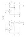
- Comparative Example 1 is a case where an STI is used for device isolation.
FIG. 3 is a plan view illustrating a layout example of the first circuit according to Comparative Example 1. InFIG. 3 , the same reference marks as those inFIG. 2 denote the same or corresponding parts as those inFIG. 2 , and the descriptions thereof will be omitted here. Hereinafter, in the plan view of the layout, a region surrounded by a bold line denotes a diffusion layer. A diffusion layer LPa constitutes the diffusion layer of the PMOS transistors TP1 and TP2, and a diffusion layer LNa constitutes the diffusion layer of the NMOS transistors TN1 and TN2. Further, a diffusion layer LPb constitutes the diffusion layer of the PMOS transistor TP3, and a diffusion layer LN2 constitutes the diffusion layer of the NMOS transistor TN3. Hereinafter, in the layout view, a region shaded by diagonal lines denotes a metal, a region shaded by horizontal lines denotes a gate polysilicon which is a gate electrode formed by polycrystalline silicon, and a blackened region denotes a contact serving as a contact point for upper layer wiring. - A power supply wiring VDD (high potential) is disposed at the uppermost portion in
FIG. 3 , and a power supply wiring VSS (low potential) is disposed at the lowermost portion. The PMOS transistors are arranged on the VDD side, and the NMOS transistors are arranged on the VSS side. As the PMOS transistors, the PMOS transistors TP2, TP1, and TP3 are arranged in this order from the left. As the NMOS transistors, the NMOS transistors TN2, TN1, and TN3 are arranged in this order from the left. - IN1 is a gate electrode of the transistors TP1 and TN1, and IN2 is a gate electrode of the transistors TP2 and TN2. A (SN1) is a drain electrode of the transistors TP1, TN1, and TP2 and a gate electrode of the transistors TP3 and TN3. OUT is a drain electrode of the transistors TP3 and TN3. SP2 is a source electrode of the transistor TP2, SP1 is a source electrode of the transistor TP1, and SN2 is a source electrode of the transistor TN2. SP3 is a source electrode of the transistor TP3, and SN3 is a source electrode of the transistor TN3.
FIG. 4 is a cross-sectional view illustrating a layout example of the first circuit according to Comparative Example 1. InFIG. 4 , the same reference marks as those inFIG. 3 denote the same or corresponding parts as those inFIG. 3 , and the descriptions thereof will be omitted here.FIG. 4 is a cross-sectional view taken along X-X' line ofFIG. 3 .- STIs are provided on the left side of the transistors TP2 and TN2, on the right side of the transistors TP3 and TN3, and between the transistors TP1, TN1 and transistors TP3, TN3, respectively. As diffusion layers, a diffusion layer LPa of the transistors TP1 and TP2, a diffusion layer LNa of the transistors TN1 and TN2, a diffusion layer LPb of the transistor TP3, and a diffusion layer LNb of the transistor TN3 are provided. That is, the diffusion layer of the 2-NAND circuit and diffusion layer of the INV circuit are isolated from each other by the STI.
- According to Comparative Example 1, the diffusion layers of the 2-NAND circuit and INV circuit are isolated from each other by the STI and, correspondingly, the size of the diffusion layers is reduced, so that the effect of a strained silicon is small. Further, the transistor performance deteriorates due to a compression stress from the STI.
- Comparative Example 2 is a case where a dummy transistor is used for device isolation in place of the STI.
FIG. 5 is a plan view illustrating a layout example of the first circuit according to Comparative Example 2. InFIG. 5 , the same reference marks as those inFIG. 3 denote the same or corresponding parts as those inFIG. 3 , and the descriptions thereof will be omitted here.FIG. 6 is a cross-sectional view illustrating a layout example of the first circuit according to Comparative Example 2. InFIG. 6 , the same reference marks as those inFIG. 5 denote the same or corresponding parts as those inFIG. 5 , and the descriptions thereof will be omitted here.FIG. 6 is a cross-sectional view taken along X-X' line ofFIG. 5 . - In Comparative Example 2, the PMOS transistors TP1 and TP3 are isolated from each other by a dummy transistor XP, and the NMOS transistors TN1 and TN3 are isolated from each other by a dummy transistor XN. A gate electrode EP0 of the dummy transistor XP is provided between the source electrodes SP1 and SP3, and a gate electrode EN0 is provided as an enable terminal of the dummy transistor XN between the source electrodes SN1 and SN3. As a result, all the PMOS transistors TP1, TP2, XP, and TP3 are formed on one continuous diffusion layer LP0, and all the NMOS transistors TN1, TN2, XN, and TN3 are formed on one continuous diffusion layer LN0.
- When the gate electrode EP0 is connected to the VDD, the dummy transistor XP is kept in an OFF state. Further, when the gate electrode EN0 serving as the enable terminal is connected to the VSS, the dummy transistor XN is kept in an OFF state.
- According to Comparative Example 2, the problem of Comparative Example 1 can be solved. However, since only transistors having the same characteristics can be constructed in one diffusion layer, the performance of the transistor is constrained.
- In the present embodiment, a semiconductor device in which two dummy transistors are provided between two devices and thereby different channel widths W can be set for the two devices will be described.
FIG. 7 is a circuit diagram illustrating the details of a configuration of the first circuit according to the first embodiment. InFIG. 7 , the same reference marks as those inFIG. 2 denote the same or corresponding parts as those inFIG. 2 , and the descriptions thereof will be omitted here. The circuit ofFIG. 7 is obtained by adding the dummy PMOS transistors XP1 and XP2 and dummy NMOS transistors XN1 and XN2 to the circuit ofFIG. 2 .FIG. 8 is a plan view illustrating a layout example of the first circuit according to the first embodiment. InFIG. 8 , the same reference marks as those inFIG. 5 denote the same or corresponding parts as those inFIG. 5 , and the descriptions thereof will be omitted here. Further,FIG. 8 illustrates the layout of the circuit ofFIG. 7 .FIG. 9 is a cross-sectional view illustrating a layout example of the first circuit according to the first embodiment. InFIG. 9 , the same reference marks as those inFIG. 8 denote the same or corresponding parts as those inFIG. 8 , and the descriptions thereof will be omitted here.FIG. 9 is a cross-sectional view taken along X-X' line ofFIG. 8 .- In the present embodiment, PMOS transistors TP1 (first transistor) and TP3 (second transistor) are isolated from each other by dummy transistors XP1 (third transistor) and XP2 (fourth transistor), and NMOS transistors TN1 (first transistor) and TN3 (second transistor) are isolated from each other by dummy transistors XN1 (third transistor) and XN2 (fourth transistor).
- A gate electrode EP1 of the dummy transistor XP1 is provided between the source electrodes SP1 and SP3, a gate electrode EP2 of the dummy transistor XP2 is provided between the gate electrode EP1 and source electrode SP3, and a drain electrode FP of the dummy transistors XP1 and XP2 is provided between the gate electrodes EP1 and EP2. Similarly, a gate electrode EN1 is provided as an enable terminal of the dummy transistor XN1 between the source electrodes SN1 and SN3, a gate electrode EN2 is provided as an enable terminal of the dummy transistor XN2 between the gate electrode EN1 and source electrode SN3, and a drain electrode FN of the dummy transistors XN1 and XN2 is provided between the gate electrodes EN1 and EN2. Although there are provided in this example the drain electrode FP which is connected to the VDD so as to make the potentials of the drains of the dummy transistors XP1 and XP2 constant and the drain electrode FN which is connected to the VSS so as to make the potentials of the drains of the dummy transistors XN1 and XN2 constant, the drain electrodes FP and FN need not always be provided.
- Thus, all the PMOS transistors TP1, TP2, XP1, XP2, and TP3 are formed on one continuous diffusion layer LP1, and all the NMOS transistors TN1, TN2, XN1, XN2, and TN3 are formed on one continuous diffusion layer LN1.
- When the gate electrodes EP1 and EP2 are connected to the VDD, the dummy transistors XP1 and XP2 are kept in an OFF state. Similarly, when the gate electrodes EN1 and EN2 serving as the enable terminals are connected to the VSS, the dummy transistors XN1 and XN2 are kept in an OFF state. That is, existence of the dummy transistors XP1, XP2, XN1, and XN2 does not affect the function of the first circuit.
- In the present embodiment, the channel width W of the diffusion layer LP1 is changed between the dummy transistors XP1 and XP2. That is, in the diffusion layer LP1, the channel width W of a region LPa (first diffusion region) where the transistors TP1, TP2, and XP1 are formed is set to W1, and the channel width W of a region LPb (second diffusion region) where the transistors XP2 and TP3 are formed is set to W2. Similarly, the channel width W of the diffusion layer LN1 is changed between the XN1 and XN2. That is, in the diffusion layer LN1, the channel width W of a region LNa (first diffusion region) where the transistors TN1, TN2, and XN1 are formed is set to W3, and the channel width W of a region LNb (second diffusion region) where the transistors XN2 and TN3 are formed is set to W4.
- By providing the two dummy transistors in one diffusion layer, it is possible to define the boundary of the channel width between the two dummy transistors. Therefore, a fixed channel width can be set for the left side region of the one diffusion layer LP1 starting from the dummy transistor XP1 and extending to the left and another fixed channel width can be set for the right side region of the one diffusion layer LP1 starting from the dummy transistor XP2 and extending to the right. Similarly, a fixed channel width can be set for the left side region of the one diffusion layer LN1 starting from the dummy transistor XN1 and extending to the left and another fixed channel width can be set for the right side region of the one diffusion layer LN1 starting from the dummy transistor XN2 and extending to the right.
- According to the present embodiment, by forming the diffusion layer in a continuous manner across a plurality of circuits, it is possible to eliminate the need to provide the STI which may cause the deterioration of the transistor performance and to enhance the effect of the strained silicon. Further, by providing the two dummy transistors between two devices, it is possible to set different channel widths W for the two devices. Thus, the value of the channel width can be made different region by region in one continuous diffusion layer, allowing design of a transistor having appropriate channel widths for respective circuits. That is, even in the case where there occurs a need to change the value of the channel width in order to optimize transistor characteristics for each region in the continuous diffusion layer, a transistor having optimum channel width can be obtained by forming the dummy transistors in the region at which the channel width is changed.
- In the present embodiment, a semiconductor device in which two dummy transistors are provided between two devices and thereby different threshold voltages Vth can be set for the two devices will be described.
FIG. 10 is a plan view illustrating a layout example of the first circuit according to the second embodiment. InFIG. 10 , the same reference marks as those inFIG. 8 denote the same or corresponding parts as those inFIG. 8 , and the descriptions thereof will be omitted here. As withFIG. 8 ,FIG. 10 illustrates the layout of the circuit ofFIG. 7 .FIG. 11 is a cross-sectional view illustrating a layout example of the first circuit according to the second embodiment. InFIG. 11 , the same reference marks as those inFIG. 10 denote the same or corresponding parts as those inFIG. 10 , and the descriptions thereof will be omitted here.FIG. 11 is a cross-sectional view taken along X-X' line ofFIG. 10 .- As in the case of the first embodiment, all the PMOS transistors TP1, TP2, XP1, XP2, and TP3 are formed on one continuous diffusion layer LP1, and all the NMOS transistors TN1, TN2, XN1, XN2, and TN3 are formed on one continuous diffusion layer LN1.
- In the present embodiment, the dose amount of a region (first diffusion region) where the transistors TP1, TP2, and XP1 are formed and does amount of a region (second diffusion region) where the transistors XP2 and TP3 are formed are made different to thereby set the value of the threshold voltage Vth of the PMOS transistors TP1 and TP2 to Vthp1 and the value of the threshold voltage Vth of the PMOS transistors TP3 to Vthp2. The dose amount denotes an electron or ion injection amount per unit area of the silicon substrate. Similarly, the dose amount of a region (first diffusion region) where the NMOS transistors TN1, TN2, and XN1 are formed and does amount of a region (second diffusion region) where the transistors XN2 and TN3 are formed are made different to thereby set the value of the threshold voltage of the transistors TN1 and TN2 to Vthn1 and the value of the threshold voltage of the transistors TN3 to Vthn2.
- For example, an ion injection mask for normal threshold voltage is used to conduct ion injection to the region where the transistors XP2 and TP3 are formed and region where the transistors XN2 and TN3 are formed, while an ion injection mask for high threshold voltage is used to conduct ion injection to the region where the transistors TP1, TP2, and XP1 are formed and region where the transistors TN1, TN2, and XN1 are formed. As a result, the threshold voltages Vthp1 and Vthn1 of the transistors TP1, TP2, TN1, and TN2 can be made higher than the threshold voltages Vthp2 and Vthn2 of the transistors TP3 and TN3.
- Further, as in the case of the first embodiment, in the diffusion layer LP1, the channel width W of the region where the transistors TP1, TP2, and XP1 are formed is set to W1, and the channel width W of the region where the transistors XP2 and TP3 are formed is set to W2. Similarly, in the diffusion layer LN1, the channel width W of the region where the transistors TN1, TN2, and XN1 are formed is set to W3, and the channel width W of the region where the transistors XN2 and TN3 are formed is set to W4.
- By providing the two dummy transistors in one diffusion layer LP1, it is possible to define the boundary of the threshold voltage between the two dummy transistors. Therefore, a fixed threshold voltage can be set for the left side region of the one diffusion layer LP1 starting from the dummy transistor XP1 and extending to the left and another fixed threshold voltage can be set for the right side region of the one diffusion layer LP1 starting from the dummy transistor XP2 and extending to the right. Similarly, a fixed threshold voltage can be set for the left side region of the one diffusion layer LN1 starting from the dummy transistor XN1 and extending to the left and another threshold voltage width can be set for the right side region of the one diffusion layer LN1 starting from the dummy transistor XN2 and extending to the right.
- According to the present embodiment, by forming the diffusion layer in a continuous manner across a plurality of circuits, it is possible to eliminate the need to provide the STI which may cause the deterioration of the transistor performance and to enhance the effect of the strained silicon. Further, the value of the threshold voltage can be made different region by region in one continuous diffusion layer, allowing design of a transistor having appropriate threshold voltage values for respective circuits.
- Although both the channel width and threshold voltage are made different between the regions which are isolated from each other by the dummy transistors in the present embodiment, only the threshold voltage may be made different between the regions.
- In the present embodiment, a semiconductor device in which two dummy transistors are provided between two devices and thereby stable power supply to the two devices can be achieved will be described.
- First, a second circuit exemplified as a circuit will be described. The second circuit has a first 2-NAND (2-input negative logical multiplication) circuit and a second 2-NAND circuit.
FIG. 12 is a circuit diagram illustrating the outline of a configuration of the second circuit. The first 2-NAND circuit receives as inputs IN1a and IN2a and outputs OUTa. The first 2-NAND circuit receives as inputs IN1b and IN2b and outputs OUTb.FIG. 13 is a circuit diagram illustrating the details of the configuration of the second circuit. The first 2-NAND circuit is constituted by PMOS transistors TP1a, TP2a and NMOS transistors TN1a, TN2a. The second 2-NAND circuit is constituted by PMOS transistors TP1b, TP2b and NMOS transistors TN1b, TN2b.FIG. 14 is a circuit diagram illustrating the details of a configuration of the second circuit according to the third embodiment. InFIG. 14 , the same reference marks as those inFIG. 13 denote the same or corresponding parts as those inFIG. 13 , and the descriptions thereof will be omitted here. The circuit ofFIG. 14 is obtained by adding the dummy PMOS transistors XP3 and dummy NMOS transistor XN3 to the circuit ofFIG. 13 .FIG. 15 is a plan view illustrating a layout example of the second circuit according to the third embodiment.FIG. 15 illustrates the layout of the circuit ofFIG. 14 . As in the case of the first embodiment, a power supply wiring VDD (high potential) is disposed at the uppermost portion inFIG. 15 , and a power supply wiring VSS (low potential) is disposed at the lowermost portion. The PMOS transistors are arranged on the VDD side, and the NMOS transistors are arranged on the VSS side. As the PMOS transistors, the transistors TP2a, TP1a, XP3, TP1b, and TP2b are arranged in this order from the left. As the NMOS transistors, the transistors TN2a, TN 1 a, XN3, TN1 b, and TN2b are arranged in this order from the left.- In the present embodiment, PMOS transistors TP1a (fifth transistor) and TP1 b (sixth transistor) are isolated from each other by dummy transistors XP3 (seventh transistor), and NMOS transistors TN1a (fifth transistor) and TN1b (sixth transistor) are isolated from each other by dummy transistors XN3 (seventh transistor).
- IN1a is a gate electrode of the transistors TP1a and TN1a, and IN2a is a gate electrode of the TP2a and TN2a. IN1b is a gate electrode of the TP1b and TN1b, and IN2b is a gate electrode of the TP2b and TN2b. OUTa is a drain electrode of the TP1 a, TP2a, and TN2a. OUTb is a drain electrode of the TP1 b, TP2b, and TN2b. SP1a is a source electrode of the TP1a, and SN1a is a source electrode of the TN1a. SP2a is a source electrode of the TP2a. SP1b is a source electrode of the TP1b, and SN1b is a source electrode of the TN1b, and SP2b is a source electrode of the TP2b.
- In the present embodiment, the TP1a and TP1b are isolated from each other by a dummy transistor XP3 and the TN1a and TN1b are isolated from each other by a dummy transistor XN3. A gate electrode EP3 of the XP3 is provided between the SP1a and SP1b, and a gate electrode EN3 is provided as an enable terminal of the XN3 between the SN1a and SN1b. As a result, all the PMOS transistors TP2a, TP1a, XP3, TP1b, and TP2b are formed on one continuous diffusion layer LP3 (diffusion region), and all the NMOS transistors TN2a, TN1a, XN3, TN1b, and TN2b are formed on one continuous diffusion layer LN3 (diffusion region).
- When the gate electrode EP3 is connected to the VSS, the dummy transistor XP3 is kept in an ON state. Further, the gate electrode EP3 is connected to the VDD, the dummy transistor XN3 is kept in an ON state. That is, existence of the dummy transistors XP3 and XN3 does not affect the function of the second circuit.
- In the case where the source electrodes SP1a and SP1b connected to the power supply wiring are disposed close to each other, the dummy transistor XP3 is provided between the source electrodes SP1a and SP1b, thereby reducing power supply noise in the power supply wiring VDD by an electrostatic capacitance of the dummy transistor XP3 connecting the power supply wirings. Similarly, in the case where the source electrodes SP1a and SP1b connected to the power supply wiring are disposed close to each other, the dummy transistor XN3 is provided between the source electrodes SN1a and SN1b, thereby reducing power supply noise in the power supply wiring VDD by an electrostatic capacitance of the dummy transistor XN3 connecting the power supply wirings.
- According to the present embodiment, by forming the diffusion layer in a continuous manner across a plurality of circuits, it is possible to eliminate the need to provide the STI which may cause the deterioration of the transistor performance and to enhance the effect of the strained silicon. Further, by providing the dummy transistors, it is possible to reduce the power supply noise to thereby make the circuit operation stable.
- According to the embodiments of the present invention, it is possible to improve the performance of a circuit in the case where a plurality of circuits are arranged in a continuous diffusion layer.
Claims (13)
- A semiconductor device in a continuous diffusion region formed on a semiconductor substrate and having either a P-type or N-type polarity, the device comprising:a first transistor formed within the continuous diffusion region;a second transistor formed within the continuous diffusion region and in an area that is different from an area where the first transistor is formed;a third transistor formed within the continuous diffusion region and in an area between the first and second transistors, and having a gate electrode to which a fixed potential is applied; anda fourth transistor formed within the continuous diffusion region and in an area between the second and third transistors, and having a gate electrode to which a fixed potential is applied.
- The semiconductor device according to claim 1, comprising:two sets of the first, second, third, and fourth transistors, whereinin one of the two sets, the first, second, third, and fourth transistors are PMOS transistors, andin other one of the two sets, the first, second, third, and fourth transistors are NMOS transistors.
- The semiconductor device according to claim 1, wherein
the third and fourth transistors are kept in an OFF state. - The semiconductor device according to claim 1, wherein
the gate electrodes of the third and fourth transistors are connected to a power supply. - The semiconductor device according to claim 4, wherein
the gate electrodes of the third and fourth transistors are connected to the power supply connected to the first and second transistors. - The semiconductor device according to claim 1, further comprising, between the gate electrodes of the third and fourth transistors, an electrode connected to a power supply.
- The semiconductor device according to claim 1, wherein
the electrode connected to the power supply is a drain electrode of the third and fourth transistors. - The semiconductor device further comprising:a second continuous diffusion region formed on the semiconductor substrate and having a different type polarity from the continuous diffusion region;a fifth transistor formed within the second continuous diffusion region;a sixth transistor formed within the second continuous diffusion region and in an area that is different from the area where the fifth transistor is formed;a seventh transistor formed within the second continuous diffusion region and in an area between the fifth and sixth transistors, and having a gate electrode to which a fixed potential is applied; andan eighth transistor formed within the second continuous diffusion region and in an area between the sixth and seventh transistors, and having a gate electrode to which a fixed potential is applied.
- The semiconductor device according to claim 8, comprising:two sets of the fifth, sixth, and seventh transistors, whereinin one of the two sets, the fifth, sixth and seventh transistors are PMOS transistors, andin other one of the two sets, the fifth, sixth and seventh transistors are NMOS transistors.
- The semiconductor device according to claim 8, wherein
a fixed potential is applied to the gate electrode of the seventh transistor. - The semiconductor device according to claim 8, wherein
the gate electrode of the seventh transistor is connected to a power supply. - The semiconductor device according to claim 11, wherein
an electrode of the fifth transistor and an electrode of the sixth transistor are connected to a power supply, and the gate electrode of the seventh transistor adjoins the electrode of the fifth transistor and the electrode of the sixth transistor. - The semiconductor device according to claim 11, wherein
the gate electrode of the seventh transistor is connected to the power supply different from a power supply connected to the fifth and sixth transistors.
Applications Claiming Priority (1)
| Application Number | Priority Date | Filing Date | Title |
|---|---|---|---|
| PCT/JP2007/074091WO2009078069A1 (en) | 2007-12-14 | 2007-12-14 | Semiconductor device |
Publications (2)
| Publication Number | Publication Date |
|---|---|
| EP2251901A1true EP2251901A1 (en) | 2010-11-17 |
| EP2251901A4 EP2251901A4 (en) | 2012-08-29 |
Family
ID=40795196
Family Applications (1)
| Application Number | Title | Priority Date | Filing Date |
|---|---|---|---|
| EP07859821AWithdrawnEP2251901A4 (en) | 2007-12-14 | 2007-12-14 | SEMICONDUCTOR COMPONENT |
Country Status (4)
| Country | Link |
|---|---|
| US (1) | US8338864B2 (en) |
| EP (1) | EP2251901A4 (en) |
| JP (1) | JPWO2009078069A1 (en) |
| WO (1) | WO2009078069A1 (en) |
Cited By (20)
| Publication number | Priority date | Publication date | Assignee | Title |
|---|---|---|---|---|
| US8541879B2 (en) | 2007-12-13 | 2013-09-24 | Tela Innovations, Inc. | Super-self-aligned contacts and method for making the same |
| US8549455B2 (en) | 2007-08-02 | 2013-10-01 | Tela Innovations, Inc. | Methods for cell phasing and placement in dynamic array architecture and implementation of the same |
| US8552508B2 (en) | 2008-03-13 | 2013-10-08 | Tela Innovations, Inc. | Integrated circuit including cross-coupled transistors having gate electrodes formed within gate level feature layout channels with shared diffusion regions on opposite sides of two-transistor-forming gate level feature and electrical connection of transistor gates through linear interconnect conductors in single interconnect layer |
| US8653857B2 (en) | 2006-03-09 | 2014-02-18 | Tela Innovations, Inc. | Circuitry and layouts for XOR and XNOR logic |
| US8658542B2 (en) | 2006-03-09 | 2014-02-25 | Tela Innovations, Inc. | Coarse grid design methods and structures |
| US8661392B2 (en) | 2009-10-13 | 2014-02-25 | Tela Innovations, Inc. | Methods for cell boundary encroachment and layouts implementing the Same |
| US8667443B2 (en) | 2007-03-05 | 2014-03-04 | Tela Innovations, Inc. | Integrated circuit cell library for multiple patterning |
| US8680626B2 (en) | 2007-10-26 | 2014-03-25 | Tela Innovations, Inc. | Methods, structures, and designs for self-aligning local interconnects used in integrated circuits |
| US8701071B2 (en) | 2008-01-31 | 2014-04-15 | Tela Innovations, Inc. | Enforcement of semiconductor structure regularity for localized transistors and interconnect |
| US8756551B2 (en) | 2007-08-02 | 2014-06-17 | Tela Innovations, Inc. | Methods for designing semiconductor device with dynamic array section |
| US8759985B2 (en) | 2008-03-27 | 2014-06-24 | Tela Innovations, Inc. | Methods for multi-wire routing and apparatus implementing same |
| US8823062B2 (en) | 2006-03-09 | 2014-09-02 | Tela Innovations, Inc. | Integrated circuit with offset line end spacings in linear gate electrode level |
| US8839175B2 (en) | 2006-03-09 | 2014-09-16 | Tela Innovations, Inc. | Scalable meta-data objects |
| US8863063B2 (en) | 2009-05-06 | 2014-10-14 | Tela Innovations, Inc. | Finfet transistor circuit |
| US9035359B2 (en) | 2006-03-09 | 2015-05-19 | Tela Innovations, Inc. | Semiconductor chip including region including linear-shaped conductive structures forming gate electrodes and having electrical connection areas arranged relative to inner region between transistors of different types and associated methods |
| US9122832B2 (en) | 2008-08-01 | 2015-09-01 | Tela Innovations, Inc. | Methods for controlling microloading variation in semiconductor wafer layout and fabrication |
| US9159627B2 (en) | 2010-11-12 | 2015-10-13 | Tela Innovations, Inc. | Methods for linewidth modification and apparatus implementing the same |
| US9230910B2 (en) | 2006-03-09 | 2016-01-05 | Tela Innovations, Inc. | Oversized contacts and vias in layout defined by linearly constrained topology |
| US9563733B2 (en) | 2009-05-06 | 2017-02-07 | Tela Innovations, Inc. | Cell circuit and layout with linear finfet structures |
| US9754878B2 (en) | 2006-03-09 | 2017-09-05 | Tela Innovations, Inc. | Semiconductor chip including a chip level based on a layout that includes both regular and irregular wires |
Families Citing this family (12)
| Publication number | Priority date | Publication date | Assignee | Title |
|---|---|---|---|---|
| US8332794B2 (en)* | 2009-01-22 | 2012-12-11 | Taiwan Semiconductor Manufacturing Company, Ltd. | Circuits and methods for programmable transistor array |
| JP2011242541A (en)* | 2010-05-17 | 2011-12-01 | Panasonic Corp | Semiconductor integrated circuit device, and terminal structure of standard cell |
| JP5531848B2 (en)* | 2010-08-06 | 2014-06-25 | 富士通セミコンダクター株式会社 | Semiconductor device, semiconductor integrated circuit device, SRAM, and method for manufacturing Dt-MOS transistor |
| JP5695734B2 (en)* | 2011-03-04 | 2015-04-08 | ルネサスエレクトロニクス株式会社 | Semiconductor device |
| US9767058B2 (en)* | 2011-11-17 | 2017-09-19 | Futurewei Technologies, Inc. | Method and apparatus for scalable low latency solid state drive interface |
| US8836040B2 (en)* | 2012-11-07 | 2014-09-16 | Qualcomm Incorporated | Shared-diffusion standard cell architecture |
| US20140246725A1 (en)* | 2013-03-04 | 2014-09-04 | Samsung Electronics Co., Ltd. | Integrated Circuit Memory Devices Including Parallel Patterns in Adjacent Regions |
| US9190405B2 (en) | 2014-01-31 | 2015-11-17 | Qualcomm Incorporated | Digital circuit design with semi-continuous diffusion standard cell |
| US9318476B2 (en)* | 2014-03-03 | 2016-04-19 | Qualcomm Incorporated | High performance standard cell with continuous oxide definition and characterized leakage current |
| US10361195B2 (en) | 2014-09-04 | 2019-07-23 | Samsung Electronics Co., Ltd. | Semiconductor device with an isolation gate and method of forming |
| US10692808B2 (en) | 2017-09-18 | 2020-06-23 | Qualcomm Incorporated | High performance cell design in a technology with high density metal routing |
| WO2019116883A1 (en)* | 2017-12-12 | 2019-06-20 | 株式会社ソシオネクスト | Semiconductor integrated circuit device |
Family Cites Families (14)
| Publication number | Priority date | Publication date | Assignee | Title |
|---|---|---|---|---|
| US5847429A (en)* | 1995-07-31 | 1998-12-08 | Integrated Device Technology, Inc. | Multiple node ESD devices |
| JPH09289251A (en)* | 1996-04-23 | 1997-11-04 | Matsushita Electric Ind Co Ltd | Layout structure of semiconductor integrated circuit and its verification method |
| DE19907921C1 (en)* | 1999-02-24 | 2000-09-28 | Siemens Ag | Semiconductor memory arrangement with dummy components in continuous diffusion areas |
| JP5028714B2 (en)* | 2001-03-30 | 2012-09-19 | 富士通セミコンダクター株式会社 | Semiconductor integrated circuit device and wiring method |
| JP4398195B2 (en) | 2003-08-08 | 2010-01-13 | パナソニック株式会社 | Semiconductor memory device |
| JP2005268610A (en)* | 2004-03-19 | 2005-09-29 | Matsushita Electric Ind Co Ltd | Standard cell design method and semiconductor integrated circuit |
| JP4778689B2 (en)* | 2004-06-16 | 2011-09-21 | パナソニック株式会社 | Standard cells, standard cell libraries, and semiconductor integrated circuits |
| JP2006210453A (en) | 2005-01-26 | 2006-08-10 | Sony Corp | Semiconductor device |
| JP4564469B2 (en) | 2005-07-07 | 2010-10-20 | パナソニック株式会社 | Semiconductor device |
| CN1893085A (en) | 2005-07-07 | 2007-01-10 | 松下电器产业株式会社 | Semiconductor device and method for fabricating the same |
| JP2007027272A (en) | 2005-07-13 | 2007-02-01 | Toshiba Corp | Semiconductor integrated circuit |
| KR100665850B1 (en)* | 2005-07-22 | 2007-01-09 | 삼성전자주식회사 | Arrangement Structure and Arrangement Method of Morse Transistors for Highly Integrated Semiconductor Memory Devices |
| US7259393B2 (en)* | 2005-07-26 | 2007-08-21 | Taiwan Semiconductor Manufacturing Co. | Device structures for reducing device mismatch due to shallow trench isolation induced oxides stresses |
| JP2007311491A (en)* | 2006-05-17 | 2007-11-29 | Toshiba Corp | Semiconductor integrated circuit |
- 2007
- 2007-12-14WOPCT/JP2007/074091patent/WO2009078069A1/ennot_activeCeased
- 2007-12-14EPEP07859821Apatent/EP2251901A4/ennot_activeWithdrawn
- 2007-12-14JPJP2009546084Apatent/JPWO2009078069A1/enactivePending
- 2010
- 2010-06-07USUS12/794,966patent/US8338864B2/ennot_activeExpired - Fee Related
Cited By (104)
| Publication number | Priority date | Publication date | Assignee | Title |
|---|---|---|---|---|
| US8823062B2 (en) | 2006-03-09 | 2014-09-02 | Tela Innovations, Inc. | Integrated circuit with offset line end spacings in linear gate electrode level |
| US10230377B2 (en) | 2006-03-09 | 2019-03-12 | Tela Innovations, Inc. | Circuitry and layouts for XOR and XNOR logic |
| US10217763B2 (en) | 2006-03-09 | 2019-02-26 | Tela Innovations, Inc. | Semiconductor chip having region including gate electrode features of rectangular shape on gate horizontal grid and first-metal structures of rectangular shape on at least eight first-metal gridlines of first-metal vertical grid |
| US10186523B2 (en) | 2006-03-09 | 2019-01-22 | Tela Innovations, Inc. | Semiconductor chip having region including gate electrode features formed in part from rectangular layout shapes on gate horizontal grid and first-metal structures formed in part from rectangular layout shapes on at least eight first-metal gridlines of first-metal vertical grid |
| US10141334B2 (en) | 2006-03-09 | 2018-11-27 | Tela Innovations, Inc. | Semiconductor chip including region having rectangular-shaped gate structures and first-metal structures |
| US10141335B2 (en) | 2006-03-09 | 2018-11-27 | Tela Innovations, Inc. | Semiconductor CIP including region having rectangular-shaped gate structures and first metal structures |
| US9917056B2 (en) | 2006-03-09 | 2018-03-13 | Tela Innovations, Inc. | Coarse grid design methods and structures |
| US9905576B2 (en) | 2006-03-09 | 2018-02-27 | Tela Innovations, Inc. | Semiconductor chip including region having rectangular-shaped gate structures and first metal structures |
| US9859277B2 (en) | 2006-03-09 | 2018-01-02 | Tela Innovations, Inc. | Methods, structures, and designs for self-aligning local interconnects used in integrated circuits |
| US9754878B2 (en) | 2006-03-09 | 2017-09-05 | Tela Innovations, Inc. | Semiconductor chip including a chip level based on a layout that includes both regular and irregular wires |
| US9741719B2 (en) | 2006-03-09 | 2017-08-22 | Tela Innovations, Inc. | Methods, structures, and designs for self-aligning local interconnects used in integrated circuits |
| US9711495B2 (en) | 2006-03-09 | 2017-07-18 | Tela Innovations, Inc. | Oversized contacts and vias in layout defined by linearly constrained topology |
| US8653857B2 (en) | 2006-03-09 | 2014-02-18 | Tela Innovations, Inc. | Circuitry and layouts for XOR and XNOR logic |
| US8658542B2 (en) | 2006-03-09 | 2014-02-25 | Tela Innovations, Inc. | Coarse grid design methods and structures |
| US9673825B2 (en) | 2006-03-09 | 2017-06-06 | Tela Innovations, Inc. | Circuitry and layouts for XOR and XNOR logic |
| US9589091B2 (en) | 2006-03-09 | 2017-03-07 | Tela Innovations, Inc. | Scalable meta-data objects |
| US9443947B2 (en) | 2006-03-09 | 2016-09-13 | Tela Innovations, Inc. | Semiconductor chip including region having integrated circuit transistor gate electrodes formed by various conductive structures of specified shape and position and method for manufacturing the same |
| US9425145B2 (en) | 2006-03-09 | 2016-08-23 | Tela Innovations, Inc. | Oversized contacts and vias in layout defined by linearly constrained topology |
| US9425272B2 (en) | 2006-03-09 | 2016-08-23 | Tela Innovations, Inc. | Semiconductor chip including integrated circuit including four transistors of first transistor type and four transistors of second transistor type with electrical connections between various transistors and methods for manufacturing the same |
| US9425273B2 (en) | 2006-03-09 | 2016-08-23 | Tela Innovations, Inc. | Semiconductor chip including integrated circuit including at least five gate level conductive structures having particular spatial and electrical relationship and method for manufacturing the same |
| US9336344B2 (en) | 2006-03-09 | 2016-05-10 | Tela Innovations, Inc. | Coarse grid design methods and structures |
| US9240413B2 (en) | 2006-03-09 | 2016-01-19 | Tela Innovations, Inc. | Methods, structures, and designs for self-aligning local interconnects used in integrated circuits |
| US9230910B2 (en) | 2006-03-09 | 2016-01-05 | Tela Innovations, Inc. | Oversized contacts and vias in layout defined by linearly constrained topology |
| US9035359B2 (en) | 2006-03-09 | 2015-05-19 | Tela Innovations, Inc. | Semiconductor chip including region including linear-shaped conductive structures forming gate electrodes and having electrical connection areas arranged relative to inner region between transistors of different types and associated methods |
| US9009641B2 (en) | 2006-03-09 | 2015-04-14 | Tela Innovations, Inc. | Circuits with linear finfet structures |
| US8952425B2 (en) | 2006-03-09 | 2015-02-10 | Tela Innovations, Inc. | Integrated circuit including at least four linear-shaped conductive structures having extending portions of different length |
| US8946781B2 (en) | 2006-03-09 | 2015-02-03 | Tela Innovations, Inc. | Integrated circuit including gate electrode conductive structures with different extension distances beyond contact |
| US8921896B2 (en) | 2006-03-09 | 2014-12-30 | Tela Innovations, Inc. | Integrated circuit including linear gate electrode structures having different extension distances beyond contact |
| US8921897B2 (en) | 2006-03-09 | 2014-12-30 | Tela Innovations, Inc. | Integrated circuit with gate electrode conductive structures having offset ends |
| US8839175B2 (en) | 2006-03-09 | 2014-09-16 | Tela Innovations, Inc. | Scalable meta-data objects |
| US9633987B2 (en) | 2007-03-05 | 2017-04-25 | Tela Innovations, Inc. | Integrated circuit cell library for multiple patterning |
| US10074640B2 (en) | 2007-03-05 | 2018-09-11 | Tela Innovations, Inc. | Integrated circuit cell library for multiple patterning |
| US8667443B2 (en) | 2007-03-05 | 2014-03-04 | Tela Innovations, Inc. | Integrated circuit cell library for multiple patterning |
| US9424387B2 (en) | 2007-03-07 | 2016-08-23 | Tela Innovations, Inc. | Methods for cell phasing and placement in dynamic array architecture and implementation of the same |
| US8966424B2 (en) | 2007-03-07 | 2015-02-24 | Tela Innovations, Inc. | Methods for cell phasing and placement in dynamic array architecture and implementation of the same |
| US9910950B2 (en) | 2007-03-07 | 2018-03-06 | Tela Innovations, Inc. | Methods for cell phasing and placement in dynamic array architecture and implementation of the same |
| US9595515B2 (en) | 2007-03-07 | 2017-03-14 | Tela Innovations, Inc. | Semiconductor chip including integrated circuit defined within dynamic array section |
| US8756551B2 (en) | 2007-08-02 | 2014-06-17 | Tela Innovations, Inc. | Methods for designing semiconductor device with dynamic array section |
| US8759882B2 (en) | 2007-08-02 | 2014-06-24 | Tela Innovations, Inc. | Semiconductor device with dynamic array sections defined and placed according to manufacturing assurance halos |
| US8549455B2 (en) | 2007-08-02 | 2013-10-01 | Tela Innovations, Inc. | Methods for cell phasing and placement in dynamic array architecture and implementation of the same |
| US8680626B2 (en) | 2007-10-26 | 2014-03-25 | Tela Innovations, Inc. | Methods, structures, and designs for self-aligning local interconnects used in integrated circuits |
| US10734383B2 (en) | 2007-10-26 | 2020-08-04 | Tela Innovations, Inc. | Methods, structures, and designs for self-aligning local interconnects used in integrated circuits |
| US9818747B2 (en) | 2007-12-13 | 2017-11-14 | Tela Innovations, Inc. | Super-self-aligned contacts and method for making the same |
| US8541879B2 (en) | 2007-12-13 | 2013-09-24 | Tela Innovations, Inc. | Super-self-aligned contacts and method for making the same |
| US10461081B2 (en) | 2007-12-13 | 2019-10-29 | Tel Innovations, Inc. | Super-self-aligned contacts and method for making the same |
| US9281371B2 (en) | 2007-12-13 | 2016-03-08 | Tela Innovations, Inc. | Super-self-aligned contacts and method for making the same |
| US8951916B2 (en) | 2007-12-13 | 2015-02-10 | Tela Innovations, Inc. | Super-self-aligned contacts and method for making the same |
| US9530734B2 (en) | 2008-01-31 | 2016-12-27 | Tela Innovations, Inc. | Enforcement of semiconductor structure regularity for localized transistors and interconnect |
| US8701071B2 (en) | 2008-01-31 | 2014-04-15 | Tela Innovations, Inc. | Enforcement of semiconductor structure regularity for localized transistors and interconnect |
| US9202779B2 (en) | 2008-01-31 | 2015-12-01 | Tela Innovations, Inc. | Enforcement of semiconductor structure regularity for localized transistors and interconnect |
| US8680583B2 (en) | 2008-03-13 | 2014-03-25 | Tela Innovations, Inc. | Integrated circuit including cross-coupled transistors having gate electrodes formed within at least nine gate level feature layout channels |
| US8569841B2 (en) | 2008-03-13 | 2013-10-29 | Tela Innovations, Inc. | Integrated circuit including cross-coupled transistors having gate electrodes formed within gate level feature layout channels with at least one gate level feature extending into adjacent gate level feature layout channel |
| US8735995B2 (en) | 2008-03-13 | 2014-05-27 | Tela Innovations, Inc. | Cross-coupled transistor circuit defined on three gate electrode tracks with diffusion regions of common node on opposing sides of same gate electrode track |
| US9081931B2 (en) | 2008-03-13 | 2015-07-14 | Tela Innovations, Inc. | Cross-coupled transistor circuit having diffusion regions of common node on opposing sides of same gate electrode track and gate node connection through single interconnect layer |
| US9117050B2 (en) | 2008-03-13 | 2015-08-25 | Tela Innovations, Inc. | Integrated circuit including cross-coupled transistors having gate electrodes formed within gate level feature layout channels with gate contact position and offset specifications |
| US8785978B2 (en) | 2008-03-13 | 2014-07-22 | Tela Innovations, Inc. | Integrated circuit including cross-coupled transistors having gate electrodes formed within gate level feature layout channels with electrical connection of cross-coupled transistors through same interconnect layer |
| US10727252B2 (en) | 2008-03-13 | 2020-07-28 | Tela Innovations, Inc. | Semiconductor chip including integrated circuit having cross-coupled transistor configuration and method for manufacturing the same |
| US8742462B2 (en) | 2008-03-13 | 2014-06-03 | Tela Innovations, Inc. | Integrated circuit including cross-coupled transistors having gate electrodes formed within gate level feature layout channels with gate contact position specifications |
| US9208279B2 (en) | 2008-03-13 | 2015-12-08 | Tela Innovations, Inc. | Semiconductor chip including digital logic circuit including linear-shaped conductive structures having electrical connection areas located within inner region between transistors of different type and associated methods |
| US9213792B2 (en) | 2008-03-13 | 2015-12-15 | Tela Innovations, Inc. | Semiconductor chip including digital logic circuit including at least six transistors with some transistors forming cross-coupled transistor configuration and associated methods |
| US8729643B2 (en) | 2008-03-13 | 2014-05-20 | Tela Innovations, Inc. | Cross-coupled transistor circuit including offset inner gate contacts |
| US8729606B2 (en) | 2008-03-13 | 2014-05-20 | Tela Innovations, Inc. | Integrated circuit including cross-coupled transistors having gate electrodes formed within gate level feature layout channels |
| US9245081B2 (en) | 2008-03-13 | 2016-01-26 | Tela Innovations, Inc. | Semiconductor chip including digital logic circuit including at least nine linear-shaped conductive structures collectively forming gate electrodes of at least six transistors with some transistors forming cross-coupled transistor configuration and associated methods |
| US10658385B2 (en) | 2008-03-13 | 2020-05-19 | Tela Innovations, Inc. | Cross-coupled transistor circuit defined on four gate electrode tracks |
| US8742463B2 (en) | 2008-03-13 | 2014-06-03 | Tela Innovations, Inc. | Integrated circuit including cross-coupled transistors having gate electrodes formed within gate level feature layout channels with outer positioned gate contacts |
| US10651200B2 (en) | 2008-03-13 | 2020-05-12 | Tela Innovations, Inc. | Cross-coupled transistor circuit defined on three gate electrode tracks |
| US8816402B2 (en) | 2008-03-13 | 2014-08-26 | Tela Innovations, Inc. | Integrated circuit including cross-coupled transistors having gate electrodes formed within gate level feature layout channels with gate level feature layout channel including single transistor |
| US8785979B2 (en) | 2008-03-13 | 2014-07-22 | Tela Innovations, Inc. | Integrated circuit including cross-coupled transistors having gate electrodes formed within gate level feature layout channels with two inside positioned gate contacts and two outside positioned gate contacts and electrical connection of cross-coupled transistors through same interconnect layer |
| US8872283B2 (en) | 2008-03-13 | 2014-10-28 | Tela Innovations, Inc. | Integrated circuit including cross-coupled transistors having gate electrodes formed within gate level feature layout channels with shared diffusion regions on opposite sides of two-transistor-forming gate level feature |
| US8669594B2 (en) | 2008-03-13 | 2014-03-11 | Tela Innovations, Inc. | Integrated circuit including cross-coupled transistors having gate electrodes formed within at least twelve gate level feature layout channels |
| US8866197B2 (en) | 2008-03-13 | 2014-10-21 | Tela Innovations, Inc. | Integrated circuit including cross-coupled transistors having gate electrodes formed within gate level feature layout channels with at least two gate electrodes electrically connected to each other through another transistor forming gate level feature |
| US8669595B2 (en) | 2008-03-13 | 2014-03-11 | Tela Innovations, Inc. | Integrated circuit including cross-coupled transistors having gate electrodes formed within gate level feature layout channels with gate contact position, alignment, and offset specifications |
| US8772839B2 (en) | 2008-03-13 | 2014-07-08 | Tela Innovations, Inc. | Integrated circuit including cross-coupled transistors having gate electrodes formed within gate level feature layout channels with four inside positioned gate contacts having offset and aligned relationships and electrical connection of transistor gates through linear interconnect conductors in single interconnect layer |
| US8552508B2 (en) | 2008-03-13 | 2013-10-08 | Tela Innovations, Inc. | Integrated circuit including cross-coupled transistors having gate electrodes formed within gate level feature layout channels with shared diffusion regions on opposite sides of two-transistor-forming gate level feature and electrical connection of transistor gates through linear interconnect conductors in single interconnect layer |
| US9536899B2 (en) | 2008-03-13 | 2017-01-03 | Tela Innovations, Inc. | Semiconductor chip including integrated circuit having cross-coupled transistor configuration and method for manufacturing the same |
| US8552509B2 (en) | 2008-03-13 | 2013-10-08 | Tela Innovations, Inc. | Integrated circuit including cross-coupled transistors having gate electrodes formed within gate level feature layout channels with other transistors positioned between cross-coupled transistors |
| US8853794B2 (en) | 2008-03-13 | 2014-10-07 | Tela Innovations, Inc. | Integrated circuit within semiconductor chip including cross-coupled transistor configuration |
| US8853793B2 (en) | 2008-03-13 | 2014-10-07 | Tela Innovations, Inc. | Integrated circuit including gate electrode level region including cross-coupled transistors having gate contacts located over inner portion of gate electrode level region and offset gate level feature line ends |
| US8847331B2 (en) | 2008-03-13 | 2014-09-30 | Tela Innovations, Inc. | Semiconductor chip including region having cross-coupled transistor configuration with offset electrical connection areas on gate electrode forming conductive structures and at least two different inner extension distances of gate electrode forming conductive structures |
| US8558322B2 (en) | 2008-03-13 | 2013-10-15 | Tela Innovations, Inc. | Integrated circuit including cross-coupled transistors having gate electrodes formed within gate level feature layout channels with at least two gate electrodes electrically connected to each other through gate level feature |
| US8564071B2 (en) | 2008-03-13 | 2013-10-22 | Tela Innovations, Inc. | Integrated circuit including cross-coupled transistors having gate electrodes formed within gate level feature layout channels with at least two different gate level feature extensions beyond contact |
| US8592872B2 (en) | 2008-03-13 | 2013-11-26 | Tela Innovations, Inc. | Integrated circuit including cross-coupled transistors with two transistors of different type having gate electrodes formed by common gate level feature with shared diffusion regions on opposite sides of common gate level feature |
| US8587034B2 (en) | 2008-03-13 | 2013-11-19 | Tela Innovations, Inc. | Integrated circuit including cross-coupled transistors having gate electrodes formed within gate level feature layout channels with four inside positioned gate contacts and electrical connection of transistor gates through linear interconnect conductors in single interconnect layer |
| US8581304B2 (en) | 2008-03-13 | 2013-11-12 | Tela Innovations, Inc. | Integrated circuit including cross-coupled transistors having gate electrodes formed within gate level feature layout channels with four inside positioned gate contacts having offset and aligned relationships |
| US8835989B2 (en) | 2008-03-13 | 2014-09-16 | Tela Innovations, Inc. | Integrated circuit including cross-coupled transistors having gate electrodes formed within gate level feature layout channels with gate electrode placement specifications |
| US8847329B2 (en) | 2008-03-13 | 2014-09-30 | Tela Innovations, Inc. | Cross-coupled transistor circuit defined having diffusion regions of common node on opposing sides of same gate electrode track with at least two non-inner positioned gate contacts |
| US8581303B2 (en) | 2008-03-13 | 2013-11-12 | Tela Innovations, Inc. | Integrated circuit including cross-coupled trasistors having gate electrodes formed within gate level feature layout channels with four inside positioned gate contacts having offset relationships and electrical connection of cross-coupled transistors through same interconnect layer |
| US9871056B2 (en) | 2008-03-13 | 2018-01-16 | Tela Innovations, Inc. | Semiconductor chip including integrated circuit having cross-coupled transistor configuration and method for manufacturing the same |
| US8575706B2 (en) | 2008-03-13 | 2013-11-05 | Tela Innovations, Inc. | Integrated circuit including cross-coupled transistors having gate electrodes formed within gate level feature layout channels with at least two different gate level features inner extensions beyond gate electrode |
| US8836045B2 (en) | 2008-03-13 | 2014-09-16 | Tela Innovations, Inc. | Cross-coupled transistor circuit having diffusion regions of common node on opposing sides of same gate electrode track |
| US8735944B2 (en) | 2008-03-13 | 2014-05-27 | Tela Innovations, Inc. | Integrated circuit including cross-coupled transistors having gate electrodes formed within gate level feature layout channels with serially connected transistors |
| US10020321B2 (en) | 2008-03-13 | 2018-07-10 | Tela Innovations, Inc. | Cross-coupled transistor circuit defined on two gate electrode tracks |
| US9779200B2 (en) | 2008-03-27 | 2017-10-03 | Tela Innovations, Inc. | Methods for multi-wire routing and apparatus implementing same |
| US9390215B2 (en) | 2008-03-27 | 2016-07-12 | Tela Innovations, Inc. | Methods for multi-wire routing and apparatus implementing same |
| US8759985B2 (en) | 2008-03-27 | 2014-06-24 | Tela Innovations, Inc. | Methods for multi-wire routing and apparatus implementing same |
| US9122832B2 (en) | 2008-08-01 | 2015-09-01 | Tela Innovations, Inc. | Methods for controlling microloading variation in semiconductor wafer layout and fabrication |
| US9563733B2 (en) | 2009-05-06 | 2017-02-07 | Tela Innovations, Inc. | Cell circuit and layout with linear finfet structures |
| US8863063B2 (en) | 2009-05-06 | 2014-10-14 | Tela Innovations, Inc. | Finfet transistor circuit |
| US10446536B2 (en) | 2009-05-06 | 2019-10-15 | Tela Innovations, Inc. | Cell circuit and layout with linear finfet structures |
| US8661392B2 (en) | 2009-10-13 | 2014-02-25 | Tela Innovations, Inc. | Methods for cell boundary encroachment and layouts implementing the Same |
| US9530795B2 (en) | 2009-10-13 | 2016-12-27 | Tela Innovations, Inc. | Methods for cell boundary encroachment and semiconductor devices implementing the same |
| US9269702B2 (en) | 2009-10-13 | 2016-02-23 | Tela Innovations, Inc. | Methods for cell boundary encroachment and layouts implementing the same |
| US9704845B2 (en) | 2010-11-12 | 2017-07-11 | Tela Innovations, Inc. | Methods for linewidth modification and apparatus implementing the same |
| US9159627B2 (en) | 2010-11-12 | 2015-10-13 | Tela Innovations, Inc. | Methods for linewidth modification and apparatus implementing the same |
Also Published As
| Publication number | Publication date |
|---|---|
| US8338864B2 (en) | 2012-12-25 |
| US20100244142A1 (en) | 2010-09-30 |
| EP2251901A4 (en) | 2012-08-29 |
| JPWO2009078069A1 (en) | 2011-04-28 |
| WO2009078069A1 (en) | 2009-06-25 |
Similar Documents
| Publication | Publication Date | Title |
|---|---|---|
| EP2251901A1 (en) | Semiconductor device | |
| US7808017B2 (en) | Semiconductor integrated circuit | |
| CN108807367B (en) | semiconductor device | |
| TWI392059B (en) | Planar back gate CMOS high performance capacitor | |
| US7834377B2 (en) | Semiconductor integrated circuit device | |
| US20050029556A1 (en) | Compact SRAM cell with FinFET | |
| JP2001352077A (en) | SOI field effect transistor | |
| US7703062B2 (en) | Semiconductor integrated circuit and method of designing layout of the same | |
| US7906800B2 (en) | Semiconductor integrated circuit | |
| SG173946A1 (en) | DATA PATH CELL ON AN SeOI SUBSTRATE WITH A BURIED BACK CONTROL GATE BENEATH THE INSULATING LAYER | |
| US20110049631A1 (en) | Semiconductor integrated circuit having insulated gate field effect transistors | |
| US7602019B2 (en) | Drive circuit and drain extended transistor for use therein | |
| US6635518B2 (en) | SOI FET and method for creating FET body connections with high-quality matching characteristics and no area penalty for partially depleted SOI technologies | |
| US7816212B2 (en) | Method of high voltage operation of a field effect transistor | |
| US6060748A (en) | Semiconductor integrated circuit device using a silicon-on-insulator substrate | |
| US7208798B2 (en) | Semiconductor device with an enhancement type field effect transistor in which threshold voltage is dependent upon substrate bias voltage | |
| US7728386B2 (en) | Semiconductor integrated circuit device | |
| US6420774B1 (en) | Low junction capacitance semiconductor structure and I/O buffer | |
| EP3782194B1 (en) | Body connection for a silicon-on-insulator device | |
| US20010050398A1 (en) | Ratio circuit | |
| JP3316425B2 (en) | Semiconductor integrated circuit and manufacturing method thereof | |
| JP4787554B2 (en) | Input/Output Circuit Device | |
| JP2671808B2 (en) | Interface circuit | |
| JP2007157803A (en) | Semiconductor device | |
| JPH06151741A (en) | Integrated circuit |
Legal Events
| Date | Code | Title | Description |
|---|---|---|---|
| PUAI | Public reference made under article 153(3) epc to a published international application that has entered the european phase | Free format text:ORIGINAL CODE: 0009012 | |
| 17P | Request for examination filed | Effective date:20100712 | |
| AK | Designated contracting states | Kind code of ref document:A1 Designated state(s):AT BE BG CH CY CZ DE DK EE ES FI FR GB GR HU IE IS IT LI LT LU LV MC MT NL PL PT RO SE SI SK TR | |
| AX | Request for extension of the european patent | Extension state:AL BA HR MK RS | |
| DAX | Request for extension of the european patent (deleted) | ||
| A4 | Supplementary search report drawn up and despatched | Effective date:20120727 | |
| RIC1 | Information provided on ipc code assigned before grant | Ipc:H01L 21/8234 20060101AFI20120723BHEP Ipc:H01L 27/07 20060101ALI20120723BHEP Ipc:H01L 27/092 20060101ALI20120723BHEP Ipc:H01L 27/088 20060101ALI20120723BHEP Ipc:H01L 21/765 20060101ALI20120723BHEP | |
| 17Q | First examination report despatched | Effective date:20130417 | |
| STAA | Information on the status of an ep patent application or granted ep patent | Free format text:STATUS: THE APPLICATION IS DEEMED TO BE WITHDRAWN | |
| 18D | Application deemed to be withdrawn | Effective date:20130828 |