EP2235773B1 - High current thin electrochemical cell and methods of making the same - Google Patents
High current thin electrochemical cell and methods of making the sameDownload PDFInfo
- Publication number
- EP2235773B1 EP2235773B1EP08868145.7AEP08868145AEP2235773B1EP 2235773 B1EP2235773 B1EP 2235773B1EP 08868145 AEP08868145 AEP 08868145AEP 2235773 B1EP2235773 B1EP 2235773B1
- Authority
- EP
- European Patent Office
- Prior art keywords
- layer
- cathode
- substrate
- cell
- layers
- Prior art date
- Legal status (The legal status is an assumption and is not a legal conclusion. Google has not performed a legal analysis and makes no representation as to the accuracy of the status listed.)
- Active
Links
Images


Classifications
- H—ELECTRICITY
- H01—ELECTRIC ELEMENTS
- H01M—PROCESSES OR MEANS, e.g. BATTERIES, FOR THE DIRECT CONVERSION OF CHEMICAL ENERGY INTO ELECTRICAL ENERGY
- H01M6/00—Primary cells; Manufacture thereof
- H01M6/40—Printed batteries, e.g. thin film batteries
- H—ELECTRICITY
- H01—ELECTRIC ELEMENTS
- H01M—PROCESSES OR MEANS, e.g. BATTERIES, FOR THE DIRECT CONVERSION OF CHEMICAL ENERGY INTO ELECTRICAL ENERGY
- H01M4/00—Electrodes
- H01M4/02—Electrodes composed of, or comprising, active material
- H01M4/04—Processes of manufacture in general
- H01M4/0402—Methods of deposition of the material
- H01M4/0404—Methods of deposition of the material by coating on electrode collectors
- H—ELECTRICITY
- H01—ELECTRIC ELEMENTS
- H01M—PROCESSES OR MEANS, e.g. BATTERIES, FOR THE DIRECT CONVERSION OF CHEMICAL ENERGY INTO ELECTRICAL ENERGY
- H01M4/00—Electrodes
- H01M4/02—Electrodes composed of, or comprising, active material
- H01M4/04—Processes of manufacture in general
- H01M4/0402—Methods of deposition of the material
- H01M4/0414—Methods of deposition of the material by screen printing
- H—ELECTRICITY
- H01—ELECTRIC ELEMENTS
- H01M—PROCESSES OR MEANS, e.g. BATTERIES, FOR THE DIRECT CONVERSION OF CHEMICAL ENERGY INTO ELECTRICAL ENERGY
- H01M50/00—Constructional details or processes of manufacture of the non-active parts of electrochemical cells other than fuel cells, e.g. hybrid cells
- H01M50/10—Primary casings; Jackets or wrappings
- H01M50/183—Sealing members
- H01M50/186—Sealing members characterised by the disposition of the sealing members
- H—ELECTRICITY
- H01—ELECTRIC ELEMENTS
- H01M—PROCESSES OR MEANS, e.g. BATTERIES, FOR THE DIRECT CONVERSION OF CHEMICAL ENERGY INTO ELECTRICAL ENERGY
- H01M50/00—Constructional details or processes of manufacture of the non-active parts of electrochemical cells other than fuel cells, e.g. hybrid cells
- H01M50/10—Primary casings; Jackets or wrappings
- H01M50/183—Sealing members
- H01M50/19—Sealing members characterised by the material
- H01M50/198—Sealing members characterised by the material characterised by physical properties, e.g. adhesiveness or hardness
- H—ELECTRICITY
- H01—ELECTRIC ELEMENTS
- H01M—PROCESSES OR MEANS, e.g. BATTERIES, FOR THE DIRECT CONVERSION OF CHEMICAL ENERGY INTO ELECTRICAL ENERGY
- H01M6/00—Primary cells; Manufacture thereof
- H01M6/005—Devices for making primary cells
- H—ELECTRICITY
- H01—ELECTRIC ELEMENTS
- H01M—PROCESSES OR MEANS, e.g. BATTERIES, FOR THE DIRECT CONVERSION OF CHEMICAL ENERGY INTO ELECTRICAL ENERGY
- H01M6/00—Primary cells; Manufacture thereof
- H01M6/04—Cells with aqueous electrolyte
- H01M6/06—Dry cells, i.e. cells wherein the electrolyte is rendered non-fluid
- H01M6/12—Dry cells, i.e. cells wherein the electrolyte is rendered non-fluid with flat electrodes
- Y—GENERAL TAGGING OF NEW TECHNOLOGICAL DEVELOPMENTS; GENERAL TAGGING OF CROSS-SECTIONAL TECHNOLOGIES SPANNING OVER SEVERAL SECTIONS OF THE IPC; TECHNICAL SUBJECTS COVERED BY FORMER USPC CROSS-REFERENCE ART COLLECTIONS [XRACs] AND DIGESTS
- Y02—TECHNOLOGIES OR APPLICATIONS FOR MITIGATION OR ADAPTATION AGAINST CLIMATE CHANGE
- Y02E—REDUCTION OF GREENHOUSE GAS [GHG] EMISSIONS, RELATED TO ENERGY GENERATION, TRANSMISSION OR DISTRIBUTION
- Y02E60/00—Enabling technologies; Technologies with a potential or indirect contribution to GHG emissions mitigation
- Y02E60/10—Energy storage using batteries
- Y—GENERAL TAGGING OF NEW TECHNOLOGICAL DEVELOPMENTS; GENERAL TAGGING OF CROSS-SECTIONAL TECHNOLOGIES SPANNING OVER SEVERAL SECTIONS OF THE IPC; TECHNICAL SUBJECTS COVERED BY FORMER USPC CROSS-REFERENCE ART COLLECTIONS [XRACs] AND DIGESTS
- Y02—TECHNOLOGIES OR APPLICATIONS FOR MITIGATION OR ADAPTATION AGAINST CLIMATE CHANGE
- Y02P—CLIMATE CHANGE MITIGATION TECHNOLOGIES IN THE PRODUCTION OR PROCESSING OF GOODS
- Y02P70/00—Climate change mitigation technologies in the production process for final industrial or consumer products
- Y02P70/50—Manufacturing or production processes characterised by the final manufactured product
- Y—GENERAL TAGGING OF NEW TECHNOLOGICAL DEVELOPMENTS; GENERAL TAGGING OF CROSS-SECTIONAL TECHNOLOGIES SPANNING OVER SEVERAL SECTIONS OF THE IPC; TECHNICAL SUBJECTS COVERED BY FORMER USPC CROSS-REFERENCE ART COLLECTIONS [XRACs] AND DIGESTS
- Y10—TECHNICAL SUBJECTS COVERED BY FORMER USPC
- Y10T—TECHNICAL SUBJECTS COVERED BY FORMER US CLASSIFICATION
- Y10T29/00—Metal working
- Y10T29/49—Method of mechanical manufacture
- Y10T29/49002—Electrical device making
- Y10T29/49108—Electric battery cell making
- Y10T29/49114—Electric battery cell making including adhesively bonding
Definitions
- This applicationrelates generally to an electrochemical cell or battery, and more specifically relates to a flat, thin, electrochemical cell utilizing a picture frame feature and its method of manufacture, including printing methods. Even more specifically, this invention relates to a thin printable cell comprising two or more electrodes, a separator, electrolyte, and a cell frame between two laminated film layers, and its method of manufacture.
- the thin flat power sourcescan be separately manufactured and later electrically coupled to various electronic devices.
- the Itis also known in the art (see W02005/101973 ) a battery comprising a first substrate, a cathode collector layer provided on said first substrate, a plurality of cathode layers provided on said cathode collector layer, an anode layer and also an electrolyte layer which is impregnated in the wall of the substrate and in contact with said plurality of cathode layers and said anode layer.
- manufacture of the thin flat power sourcescan be integrated with the manufacture of the desired circuitry of electrical components to power the components.
- a method of manufacturing a thin, printed battery including at least one electrochemical cell for generating an electrical currentis provided.
- the methodis defined by the subject-matter of claim 1.
- a thin, printed battery according to claim 7is provided.
- FIG. 1illustrates a plan view of prior art unit cell 600
- FIG. 2illustrates a cross section view of the prior art unit cell 600 taken through electrode areas along line 2-2 of FIG. 1 ;
- FIG. 3illustrates a cross section view of the prior art unit cell 600 taken through the entire length of the first electrode along line 3-3 of FIG. 1 ;
- FIG. 4illustrates a cross section view of the prior art unit cell 600 taken through the entire length of the second electrode along line 4-4 of FIG. 1 ;
- FIG. 5illustrates a top, partial detail view of an example high current thin electrochemical cell
- FIG. 6illustrates a cross section view of the electrochemical cell taken through line 6-6 of FIG. 5 ;
- FIG. 7illustrates a top, partial detail view of another example high current thin electrochemical cell
- FIG. 8illustrates an example continuous discharge curves relating cell voltage to discharge time for an example high current thin electrochemical cell and compared to a cell of the prior art
- FIG. 9is similar to FIG. 8 , but the cells are discharged on a different load
- FIG. 10is similar to FIG. 8 , but the cells are discharged on another different load;
- FIG. 11shows closed circuit voltages (CCV) for a two second pulse with a plurality of currents in milliamps
- FIG. 12illustrates a flow diagram of one example method of manufacturing the example high current thin electrochemical cell
- FIG. 13illustrates a plurality of example steps of the method of FIG. 12 ;
- FIG. 14illustrates another plurality of example steps of the method of FIG. 12 ;
- FIG. 15illustrates yet another plurality of example steps of the method of FIG. 12 ;
- FIG. 16illustrates a schematic view of an example manufacturing process utilizing a generally continuous web.
- the electrochemical cellsi.e., batteries
- the electrochemical cellsare typically printed and/or laminated on a continuous, flexible substrate web, and may be formed into a roll or the like.
- the individual batteriescan be removed from the roll, such as one at a time.
- the batteriescan be cut from the roll, and/or perforations of the flexible substrate roll can be provided for easy tear off.
- the batteriescan further include one or more electrical components, such as an antenna and/or a processor, for example.
- the multiple facets of this applicationcould be used in the total package described and/or they could be used individually or in any combination.
- the present applicationrelates to thin, printed electrochemical cells and/or batteries comprising a plurality of such cells.
- Such cellseach typically include at least a first electrode including a first electrochemical layer (e.g., a cathode), a second electrode including a second electrochemical layer (e.g., an anode), and an electrolyte that interacts with the electrodes to create an electrical current. All of the first and second electrodes and the electrolyte are typically contained within some structure which provides an external electrical access to the electrodes for providing an electrical current supply to some device.
- One method of mass-producing such cellsincludes depositing aqueous and/or non-aqueous solvent inks and/or other coatings in a pattern on a special substrate, such as a laminated polymeric film layer, for example.
- the depositingcan be by means of, for example, printing electrochemical inks and/or laminating a metallic foil, such as zinc foil, for example, on one or more high-speed web rotary screen printing presses, especially if the desired volumes are very high. If volumes are relatively lower, say in the quantities of only about several million or less, then relatively slower methods such as web printing with flat bed screens could be appropriate. If the volumes are even lower, such as hundreds or thousands, then a sheet-fed flat bed printing press may be utilized, for example. Still, various printing methods can be used for various desired quantities.
- the cellscan be completed (e.g., sealed, die cut, stacked and/or perforated and wound into a roll, or stacked if sheets are used on a printing press).
- This cell manufacturing processcan also be utilized for integrating one or more individual cells with an actual electronic application, or into batteries comprising multiple cells connected in series or parallel, or some combination of the two. Examples of such devices and corresponding processes will be described later, but many additional embodiments are also contemplated.
- the batterymay be described as a printed, flexible, and thin electrochemical cell.
- a cellcan include, for example, a lower film substrate that can utilize a special polymer laminate that has special features, possibly including, for example, a high moisture barrier layer in the center that is surrounded by polymer films on both sides.
- a special polymer laminatethat has special features, possibly including, for example, a high moisture barrier layer in the center that is surrounded by polymer films on both sides.
- one or both outside surfacescan be made to be print receptive for printing information, logos, instructions, identifications, serial numbers, graphics, or other information or images, as desired.
- the inner ply of the substratecould also feature a heat-sealing layer that might be co-extruded on the side opposite the barrier coating.
- a portion of the inner surface of a lower substrate layer of a cell of at least some embodimentscould utilize a cathode current collector, such as carbon, for example, printed or coated or otherwise applied on a portion of the film substrate.
- a cathode current collectorsuch as carbon, for example, printed or coated or otherwise applied on a portion of the film substrate.
- this collectorcan also be printed a layer of a relatively highly conductive ink, such as silver, nickel, or tin, for example, to improve the conductivity to the application connection, if desired.
- a relatively highly conductive inksuch as silver, nickel, or tin, for example
- a water-based ink electrochemical layeris printed as the cathode.
- a cathode layercan include, for example, manganese dioxide (MnO 2 ), carbon, and a polymer binder. Other formulations for the cathode layer can also be utilized with or without any of these materials. If a cathode collector layer is used, which may or may not form a portion of the cathode layer, the cathode electrochemical layer will be printed on at least a portion of the cathode current collector, which is printed or otherwise applied first to the substrate.
- a dry-film adhesive layerin an off-line operation, can be applied to the zinc foil.
- the zinc foilcan then be laminated to the base substrate.
- a starch ink or similar materialprinted over one or both the anode and cathode.
- the starch inkcan act as an electrolyte absorber to keep the electrodes "wet” after an aqueous electrolyte solution is added to the cell.
- This starch inkcould also include the electrolyte salts and the water used for the cell reaction.
- a paper layer over the anode and cathodecould be used in place of the printed starch.
- a cell "picture frame”can be added. This could be done using a number of different methods.
- One methodis to print this cell picture frame with a dielectric ink, for example.
- Another methodis to utilize a polymer sheet or a laminated polymer sheet that includes adhesive layers, that is stamped, die cut, laser cut or similar methods to form the appropriate "pockets" (inner space or spaces) to house materials of each unit cell as well as to expose the electrical contacts to connect the device.
- a sealing or caulking adhesivecould be printed on the substrate, such as in the same pattern as the cell frame, for example, prior to the frame being printed or prior to the polymer sheets being inserted, for example.
- This sealing or caulking materialcould be pressure sensitive, and/or heat sensitive, for example, such as Acheson Colloids' PM040, for example, or any other type of material that would facilitate sealing to both surfaces.
- a heat sensitive sealing adhesivecan be printed on top of the frame to allow good sealing of the top substrate to the cell frame.
- This cell picture framecould also comprise a polymer film or a laminated film of about 0.38 mm (0.015") thick (range of about 0.076 mm - 1.27 mm (0.003" - 0.050”)) that is pre-punched and then laminated in registration to match the preprinted caulking adhesive layer described above.
- Zinc chloridecan be chosen as the electrolyte, for at least some embodiments, in the concentration range of about 18% - 45% by weight, for example. In one example, about 27% may be preferred.
- the electrolytecan be added, for example, to the open cell. To facilitate processing on the line, this electrolyte, or a different electrolyte, could be thickened with, for example, CMC at about a level of about 0.6 wgt % (range of about 0.05 % - 1.0%).
- electrolyte formulationssuch as ammonium chloride (NH 4 Cl), mixtures of zinc chloride (ZnCl 2 ) and ammonium chloride (NH 4 Cl), zinc acetate (Zn(C 2 H 2 O 2 )), zinc bromide (ZnBr 2 ), zinc fluoride (ZnF 2 ), zinc tartrate (ZnC 4 H 4 O 6 .H 2 O), zinc per-chlorate Zn(ClO 4 ) 2 .6H 2 O), potassium hydroxide, sodium hydroxide, or organics, for example, could also be used.
- ammonium chlorideNH 4 Cl
- mixtures of zinc chlorideZnCl 2
- ammonium chlorideNH 4 Cl
- zinc acetateZn(C 2 H 2 O 2
- zinc bromideZnBr 2
- zinc fluorideZnF 2
- zinc tartrateZnC 4 H 4 O 6 .H 2 O
- Zinc chloridemay be the electrolyte of choice, providing excellent electrical performance for ordinary environmental conditions normally encountered.
- any of the above mentioned alternative electrolytes, among others,could be used in concentrations (by weight), for example, within the range of about 18% - 45%, with the range of about 25% - 35% used for at least some other embodiments.
- Such compositionscould also provide acceptable performance under ordinary environmental conditions.
- electrolytes other than of zinc chloridecan provide improved cell/battery electrical performance under some differing environmental conditions.
- about 32% by weight zinc acetate (F.P.--freezing point--about 28°C)exhibits a lower freezing point than about 32% by weight zinc chloride (F.P. about -23°C). Both of these solutions exhibit a lower freezing point than of about 27% zinc chloride (F.P. about -18°C).
- Other zinc acetate concentrationse.g. about 18-45 or about 25-35 weight percent, also exhibit reduced freezing points.
- electrolyte formulationsas substitutes for zinc chloride, or in various mixtures used in cells, can allow for improved performance at low temperatures.
- low temperaturei.e. below about -20°C
- This type of electrochemical cell performance improvement at low temperaturecan be utilized in the growing business of battery assisted RFID tags, for example, and/or other transient (transportable) electrically operated devices, such as smart active labels and temperature tags, for example, which may be used in cold environments.
- tags and/or labelsmight require electrochemical cells and/or batteries to operate effectively at temperatures at, or even below, -20°C, such as at about -23°C, about - 27°C, or even at about -30°C or less.
- the zinc acetate concentration in the range of about 31-33is often acceptable, although ranges of about 30-34, about 28-36, about 26-38, and even about 25-40, weight percent, could also be utilized.
- the construction of the printed starch layer with the addition of the aqueous electrolytecould be replaced, for example, by a printable viscous liquid (which could include a gel, or some other viscous material) that effectively covers at least a portion of each electrode.
- a printable viscous liquidwhich could include a gel, or some other viscous material
- These viscous formulationscould, for example, utilize the electrolyte formulas and concentrations previously discussed.
- the upper substrate of a cell packagecould utilize a special laminated polymeric film, which has an edge that extends beyond the internal cell/battery components onto the cell frame.
- the upper layeris sealed around the edges of the cell frame by means of a pressure sensitive adhesive (PSA), and/or with the heat sensitive sealing adhesive that was previously printed, thus confining the internal components within the cell frame.
- PSApressure sensitive adhesive
- the above-described constructionscan be wet cell constructions; however, using a similar cell construction, the battery could be also be made into a reserve cell construction, which has the benefit of providing extended shelf life prior to the application of a liquid.
- the printable, flexible, zinc chloride thin cellcan be made environmentally friendly. Such a construction could be utilized which does not require the use of harmful components, such as mercury or cadmium, for example. Old and/or depleted cells of this design could thus be disposed using regular waste removal procedures.
- the devices for which this technology can be usedare extensive. Devices that utilize relatively low power or a limited life of one to three years, and possibly longer, could function utilizing a thin cell/battery of the type described herein.
- the cellas explained in the above paragraphs and below, can often be inexpensively mass-produced so that it can be used in a disposable product, for example. The low cost allows for applications that previously were not cost effective.
- the electrochemical cell/battery according to the applicationmight have one or more of the following advantages:
- a first webcan be relatively thin, such as 0.05 mm - 0.254 mm ( ⁇ 0.002" - 0.010" ) and preferably about 0.0762 - 0.152 mm (0.003 - 0.006"), flexible base substrate including a multi-ply laminated structure or single ply material.
- the multi-ply structurecan include five layers.
- the single ply materialcan include various materials, such as Kapton or polyester.
- a second webcan be a relatively thick laminated structure including a PVC or Polyester film that is about 0.127 - 0.762 mm (0.005 - 0.030") thick, and preferably about 0.254 - 0.381 mm (0.010 - 0.015") thick.
- the second webcan have a layer of pressure sensitive adhesive at about 0.0254 - 0.127 mm (1 - 5 mils) thick on one side. After this laminated structure of the second web is completed, it can be applied to the first web.
- the second webcan be pattern cut using any type of mechanical means to allow for cavities for the cells active materials as well as an optional cavity for the cell/battery contacts.
- a third webcan be a relatively thin laminated structure the same and/or similar to the first web. The completed three web structure may have a pressure sensitive adhesive on either side to allow the individual device assembly to be applied as a label.
- the various conductive inks described hereincould be based on many types of conductive materials such as carbon, silver, nickel, silver coated copper, copper, silver chloride, zinc and/or mixtures of these.
- conductive materialssuch as carbon, silver, nickel, silver coated copper, copper, silver chloride, zinc and/or mixtures of these.
- one such material that shows useful properties in terms of conductivity and flexibilityis Acheson Colloids (Port Huron, MI) PM046.
- various circuits, electrical pathways, antennas, etc.that might be part of the printed circuitry can be made by etching aluminum, copper or similar type metallic foils that are laminated on a polymer such as Kapton substrate. This could be done with many types (sizes and frequencies) of pathways and/or antennas whether they are etched or printed.
- the prior artgenerally included a thin printed flexible electrochemical cell using a sealed "picture frame" structure, for example, that includes a printed cathode deposited on a printed cathode collector (e.g, a highly conductive carbon cathode collector) with a printed or foil strip anode placed adjacent to the cathode.
- the electrochemical cell/batteryalso includes a viscous or gelled electrolyte that is dispensed onto a separator that covers all or part of the anode and cathode, and a top laminate can then be sealed onto the picture frame.
- This type of electrochemical cellwas designed to be easily made by printing (e.g., through use of a printing press), and allows, for example, for the cell/battery to be directly integrated with an electronic application.
- FIGS. 1-4show an embodiment of a completed unit cell 600 in plan and sectional views.
- the cell 600includes a top laminated film substrate (layer) 112, a lower laminated film substrate (layer) 111, and an extended area 180 that has a silver printed positive contact 140 and negative contact 650. Additionally, the cell 600 includes a cathode layer 130 and an anode layer 116, each comprised of an electrochemical layer of a different composition that can interact through an electrolyte to create an electrical current. To provide greater clarity, cell 600 in FIG. 1 is shown without the top laminate 112.
- a cathode collector 131 of highly conductive carbonis printed on the lower laminated substrate 111.
- the cathode layer 130is printed using an ink comprising manganese dioxide, a conductor such as carbon (e.g., graphite) for example, a binder, and water.
- the anode layer 116can be printed as a conductive zinc ink, or be provided as a zinc foil (116) PSA (660) laminate as shown in the figures, either of which can be made about 5 mm (0.20") wide and about 0.05 mm (0.002") (0.0254 - 0.254 mm (0.001" - 0.010")) thick.
- a "picture frame” 113is placed around the electrodes.
- the picture frame 113can comprise a die cut polymer laminate sheet, such as a polyester or polyvinyl chloride (PVC) etc, and can be further provided with two layers of pressure sensitive adhesive (118 on the top surface and 117 on the bottom surface).
- the top pressure sensitive adhesive (PSA) layer 118seals the top laminate substrate 112 to the picture frame 113 and bottom PSA layer 117 can be used to seal the bottom laminate substrate 111 to the picture frame 113.
- the picture frame assemblyhas a total thickness (excluding the thickness of the liners) of about 0.015" (about 0.005"-0.50").
- the picture framecan be placed on the lower laminate substrate 111 after removing a bottom release liner so that the electrodes are centered within the frame.
- a sealing and/or caulking adhesive, a heat sensitive sealant, and/or double sided PSA tape 653can be placed and/or printed on top of the anode 116 and on top of cathode collector layer 131 in an area that falls under the picture frame 113.
- the sealing adhesive 653can also be provided underneath the remainder of the picture frame 113.
- a cell electrolyte 120is provided to an absorbent material such as a "paper separator" 126 (not shown in FIG. 1 for clarity, see FIG. 2 ) that covers or partially covers both electrodes.
- the electrolytecan be an aqueous solution of ZnCl 2 at weight percent of about 27% (about 23%-43%) that could also contain a thickener, such as carboxymethylcellulose (CMC) or other similar materials at about 0.6% level (about 0.1%-2%).
- CMCcarboxymethylcellulose
- a co-planar constructionprovided several advantages, in that they are easy to manufacture and provide consistent, reliable performance. However, they are designed primarily as a power sources that supply relatively low levels of current. Thus, there is an increasing need for a thin flat power source that can reliably deliver currents higher than those provided by the standard co-planar electrochemical cell construction.
- the HD designhas some significant performance advantages. These generally include one or more of the following; such as lower cathode collector resistance; lower cell internal resistance which results in higher pulse voltages on the same load; a pulse voltage improvement that is larger as the current becomes higher; and/or an increased operating time to high voltage cutoffs on higher drain tests.
- the HD design electrochemical cellwas also designed to be easily made by printing (e.g., through use of a printing press), and allows, for example, for the cell/battery to be directly integrated with an electronic application.
- the HD cell 1000generally includes a lower laminated film substrate (single or multi-layer) 1002, an upper laminated film substrate (single or multi-layer) 1004, and an extended area 1006 that has at least one positive contact 1008 and at least one negative contact 1010. Additionally, the HD cell 1000 includes a plurality of cathode layers 1012A, 1012B and at least one anode layer 1014.
- the cathode layerscan be comprised of an electrochemical layer of a different composition than the anode layer that can interact through an electrolyte to create an electrical current.
- Each of the cathode layers 1012A, 1012B and anode layer 1014can be provided on a first side of the lower substrate 1002. To provide greater clarity, HD cell 1000 in FIG. 5 is shown without the top laminate 1004.
- a cathode collector 1016 of highly conductive carboncan be printed on the lower laminated substrate 1002.
- each of the cathode layers 1012A, 1012Bis printed using an ink comprising manganese dioxide, a conductor such as carbon (e.g., graphite) for example, a binder, and water.
- a conductorsuch as carbon (e.g., graphite) for example, a binder, and water.
- Various numbers of cathode layerscan be utilized.
- the anode layer 1014can be printed as a conductive zinc ink, or as shown be provided as a zinc foil (1014) PSA (1019) laminate, either of which can be made about 5 mm (0.20") wide and about 0.05 mm (0.002") (0.0254 - 0.254 mm (0.001" - 0.010")) thick.
- An aqueous gelled coating layer(not shown) that may include ZnCl 2 electrolyte can be printed over the anode layer (not shown in FIGS. 1, and 2 ), as well as in the gaps that separates the anode layer 1014 from each of the cathode layers 1012A, 1012B.
- a dielectric layer 1018can be provided, such as printed or laminated, upon the cathode collector 1016 where the anode layer 1014 crosses thereover.
- the anode layer 1014can be insulated from said cathode collector layer 1016 by said dielectric layer 1018.
- the anode layer 1014can be printed or laminated upon the insulating dielectric layer 1018 that is provided on the cathode collector 1016.
- the insulating layer 1018can include various dielectric or electrically-neutral materials, such as polyvinyl chloride, polyester, and/or various adhesives, such as heat sensitive sealant, UV-cured sealant, and/or double sided PSA tape.
- the dielectric layer 1018 and the anode layer 1014can be disposed between at least an adjacent two of the plurality of cathode layers 1012A, 1012B.
- the dielectric layer 1018 and the anode layer 1014can be located generally equidistant between said two adjacent cathode layers 1012A, 1012B such that the electrically conductive path between the anode layer 1014 and one of the cathode layers 1012A is generally equal to the electrically conductive path between the anode layer 1014 and other of the cathode layers 1012B.
- the anode layer 1014could be disposed between an adjacent two of the plurality of cathode layers 1012A, 1012B in a non-equal fashion, such that the anode layer 1014 is closer to one of the cathode layers 1012A, 1012B.
- the anode layer 1014can be located between a pair of adjacent cathode layers 1012A, 1012B, and spaced a distance from a additional other cathode layers (not shown).
- a plurality of anode layers(not shown) can be provided and arranged variously between or near a plurality of cathode layers.
- a "picture frame" 1020can be placed around an area that will eventually bound the electrodes.
- the cathode layers 1012A, 1012Bcan be printed after the picture frame 1020 is provided if the picture frame is a printed, but before if the picture frame is a die cut polymer laminate.
- the picture frame 1020can generally be a spacer provided along the periphery of the HD electrochemical cell 1000, as viewed from the top.
- the picture frame 1020can comprise a die cut polymer laminate sheet, such as a polyester or polyvinyl chloride (PVC) etc, and can be further provided with two layers of pressure sensitive adhesive (i.e., 1022 on the top surface and 1024 on the bottom surface).
- the top pressure sensitive adhesive (PSA) layer 1022can be used to seal the top laminate substrate 1004 to the picture frame 1020
- bottom PSA layer 1024can be used to seal the bottom laminate substrate 1002 to the picture frame 1020.
- the picture frame assemblycan have a total thickness (excluding the thickness of the PSA release liners) of about 0.015" (about 0.005"-0.50").
- the picture framecan be placed on the lower laminate substrate 1002 after removing a bottom release liner so that the electrodes are centered within the frame.
- a sealing and/or caulking adhesive, a heat sensitive sealant, and/or double sided PSA tape(not shown) can be placed and/or printed on any of the dielectric layer 1018, the anode 1014, and/or cathode collector layer 1016 in an area that falls generally under the picture frame 1020.
- the sealing adhesive(not shown) can also be provided underneath the remainder of the picture frame 1020.
- the total thickness of the HD cell 1000can be generally uniform, or can vary depending upon the relative thicknesses of the various elements contained therein. If PVC is used as the spacer material, then it could be heat sealed without the use of the PSA layers on one or both sides.
- a cell electrolyte 1026can be provided to an absorbent material such as paper a paper separator 1028 or another type of soak-up material that covers or partially covers both electrodes.
- the electrolytecan be an aqueous solution of ZnCl 2 at weight percent of about 27% (about 23%-43%) that could also contain a thickener, such as carboxymethylcellulose (CMC) or other similar materials at about 0.6% level (about 0.1%-2%).
- CMCcarboxymethylcellulose
- a "starch ink" or the electrolytecould be flowed or printed over the anode and cathode that are inside the picture frame.
- the HD cell 1000is completed by applying and sealing the top laminate 1004 over the picture frame 1020 using the PSA and/or with a heat seal.
- one of the high current thin electrochemical cells described hereincan provide about 1.5 volts.
- a number of cellscan be electrically coupled together if higher voltages and/or high capacities are desired.
- a 3 volt batteryis obtained by connecting two 1.5 volt unit cells in series, although other voltages and/or currents can be obtained by using unit cells with different voltages and/or by combining different numbers of cells together either in series and/or in parallel.
- applications using greater voltagescan connect unit cells in series, whereas applications requiring greater currents and/or capacities, unit cells can be connected in parallel, and applications using both can utilize various groups of cells connected in series further connected in parallel.
- a variety of applications that use different voltages and currentscan be supported using a variety of unit cell and/or battery configuration.
- the HD design cell (2000) of FIG. 7can be constructed using non-rectilinear geometries such as circular, elliptical, triangular, square, rectangular, other polygonal shape, random, etc., as may be required for some unique applications such as medical applications.
- a generally circular shapesuch as that shown in FIG. 7 can be made more easily, and may provide a better utilization of the area inside of the picture frame between the anode and the cathodes.
- HD cell 2000 in FIG. 7is shown without the top laminate.
- the relatively increased performance characteristics of the HD cellcan be achieved with various geometries by placing the anode 2010 on top of dielectric (2016) and generally between two adjacent cathodes 2012A, 2012B.
- Similar reference numbers in the 2000 seriesi.e., 2000, 2002, etc. are used to indicate elements that are similar to, such as identical to, elements in FIG. 5 . Still, more or less various other elements can also be used.
- cells using a non-rectilinear design and including a continuous anode stripoften made for less efficient use of the anode strip and required more seal area over the anode strip. Because this area can be difficult to seal, the prior art standard construction has a greater chance for seal failure and poor electrical performance.
- the first and/or second substrates 1002, 1004can include various layers, such as five layers.
- the various layers of first substrate 1002can include three plies of film, and two layers of a UV cured urethane laminating adhesive which can be relatively thin, such as about 0.2 mils thick, with a range of about 0.1 - 0.5 mils.
- this laminated structurecan be supplied by Curwood Inc., a Bemis Corporation Company of Oshkosh, WI.
- the top film layercan be a heat sealable layer, such as provided by DuPont (OL series), which is on the inside of the cell and can have an example thickness of about 0.122 mm (0.00048") thick (e.g., about 0.0051 - 0.051 mm (0.0002" - 0.002”)).
- the middle film layercan be a high moisture barrier polymer layer such as the GL films supplied by Toppan of Japan.
- this polyester filmcan have an oxide or metalized coating on the inside of the laminated structure. This coating could have varying moisture transmission values depending on the type and the amount of vacuum deposited oxides, or metals.
- the third film layer which can be on the outside of the completed cellcan be a polyester layer that can act as a structural layer.
- This structural layer of the five ply layer structurecan be orientated polyester (OPET) and have a thickness of about 0.051 mm (0.002") (e.g., about 0.0127 - 0.0254 mm (0.0005" - 0.010")), which can also be laminated to the other layers by means of a urethane adhesive that is about 0.2 mil thick, for example.
- This "structural layer”can be a DuPont polyester orientated (OPET) film such as their Melinex brand, for example.
- Another material that can be usedis from Toyobo Co. Ltd. of Japan, which is polyester based synthetic paper, which is designated as white micro-voided orientated polyester (WMVOPET).
- the barrier layercan be chosen for each specific application and construction, as desired.
- the barrier layercan be chosen for each specific application and construction, as desired.
- Another examplewould be an application that is in a hot dry environment such as a desert or some special industrial application. In such cases, it may be desirable to have a barrier film with low transmission rates to prevent excessive moisture loss from the batteries.
- both the outside and the inside layerscould include the addition of a print-receptive surface for the inks.
- the inside layeris used for the functional inks (such as the collector and/or electrochemical layers) while the outside layer can be used for graphical inks, if desired.
- Flat cell constructions having a sealed systemmight utilize a laminated structure that includes metalized films and/or a very thin metal foil or foils as a moisture barrier. Although such structures using a metal layer might have better moisture barrier properties than the constructions used for some of the above described embodiments, it might also have some disadvantages. These may include one or more of the following:
- the various substrates described hereincan be comprised of numerous variations of polymeric film, with or without a barrier layer (including metal or other materials), and can utilize either mono-layer or multi-layer films, such as polyesters or polyolefin.
- Polyesteris a good material to utilize because it provides improved strength at the high temperature drying conditions, thus permitting use of a thinner gauge film and is typically not easily stretched when used on a multi-station printing press.
- Vinyl, cellophane, and even papercan also be used as the film layers or as one or more of the layers in the laminated constructions. If a very long shelf life is desired, and/or the environmental conditions are extreme, the multi-ply laminates could be modified to include a metalized layer such as obtained by vacuum deposition of aluminum in place of the oxide coating.
- a very thin aluminum foilcould be laminated within the structure of the film layer, or even in a different position. Such a modification could reduce already low water loss to practically nil.
- a more expensive barrier layercould be replaced with a less efficient one that would be of a lower cost and still allow the cell to function for the desired lifetime.
- the cell packagecould instead use a film layer of a low cost polymer substrate such as polyester or polyolefin.
- a heat sealing coating or the likecould be used, such as amorphous polyester (APET or PETG), semi crystalline polyester (CPET), polyvinyl chloride (PVC), or a polyolefin polymer etc. on polymer film such as polyester.
- OLOvenable Lidding
- the third substratecan be composed of various materials, such as PVC or PET film at about 0.0127 - 0.762 mm ( 0.0005" - 0.030") thick and preferably at about 0.127 - 0.381 mm (0.005" - 0.015") that is sandwiched between (i.e., interposed between) two layers of a pressure sensitive adhesive (PSA) that is about 0.0762 mm (0.003") thick (0.0254 - 0.127 mm (0.001"- 0.005")) and includes a release liner.
- PSApressure sensitive adhesive
- the spacercould be printed with a cured dielectric or some other curing and/or drying method.
- This materialsuch as Acheson Colloid's PM030, can also be a pressure sensitive adhesive, thus possibly eliminating the need to print an extra layer of adhesive.
- the anode 1014 assemblycan include various materials, such as zinc foil at about 0.0015" - 0.005" thick and preferably at about 0.0508 mm (0.002") that is laminated to a pressure sensitive adhesive (PSA) 1019 that is about 0.0508 mm (0.002") thick (0.0254 - 0.127 mm (0.001"- 0.005")) and includes release liner.
- PSApressure sensitive adhesive
- the PSA layer 1019would be disposed between the anode 1014 and the dielectric 1018.
- the HD design electrochemical cell 1000provides a generally central anode 1014 that is separated from a cathode collector 1016 by at least an insulator 1018, and also possibly by the PSA layer 1019.
- a cathode 1012A, 1012BOn each side of the anode 1014 is provided a cathode 1012A, 1012B, both of which rest on the cathode collector 1016.
- the HD electrochemical cell 1000is capable of producing a higher current due to its lower cell resistance as compared to the original construction. This is achieved by reducing the conductive length between the central anode 1014 and the two adjacent cathodes 1012A, 1012B, and/or reducing the resistance of the cathode collector 1016.
- generally symmetrical cell geometriescan be beneficial for placing the anode 1014 generally between two adjacent cathodes 1012A, 1012B to thereby reduce the distance therebetween, though various types of cell geometries can be utilized.
- the surface resistivityis the resistance between two opposite sides of a square and is independent of the size of the square or its dimensional units.
- Surface resistivitywhich is also known as "sheet resistance,” is expressed in ohms per square.
- the sheet resistanceis a measure of resistance of thin films that have a generally uniform thickness. Sheet resistance is applicable to two-dimensional systems where the thin film is considered to be a two dimensional entity. It is analogous to resistivity as used in three-dimensional systems. When the term sheet resistance is used, the current must be flowing along the plane of the sheet, and not perpendicular to it.
- the conductive lengthis the distance that current has to travel between regions of the cathode and the anode.
- the conductive lengthis substantially decreased, thus resulting in lower cell internal resistance.
- the currentscan be higher because the resistance of the cathode collector 1016 is relatively lower.
- the resistanceis lower because the number of squares is reduced.
- the resistance of the cathode collector 1016 from its bottom to its top, including the positive contact 1008,can be determined by calculating the number of squares in the cathode collector 1016. The number of squares is determined by dividing the collector length at its narrowest width by the narrowest width of the collector area.
- the number of squares using the HD designis about half of that present in a similarly sized cell using the standard construction.
- the number of squares of the instant applicationcan be generally equal to three or less.
- the number of squares of the instant applicationcan be generally equal to one, or it at least approaches one, due to an example cathode collector 1016 shape being square, or generally approaching that of a square.
- the standard construction cell of a given sizewould generally exhibit a collector resistance of about 50-70 ohms
- an HD cell of the same size using the new designwould exhibit a reduced collector resistance of about 20-40 ohms.
- the carbon inkhas a resistivity of ⁇ 20 ohms/square at one mil thick, then its theoretical resistance is about 66 ohms.
- the theoretical resistanceis about 30 ohms.
- the theoretical resistancecan be similarly determined by dividing the collector length at its narrowest width by the narrowest width of the collector area.
- the length and widthcan be determined by an effective length and an effective width, respectively.
- the effective length or widthcan be an average length or width, or other mathematically adjusted length and width that can approximate the length and width measurements of a generally rectilinear geometry.
- the theoretical resistance of the non-rectilinear collectorcan be reduced by adjusting the effective length and effective width such that the number of squares is in one example generally equal to or less than three, or in another example, generally equal to one or approaching one.
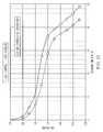
- FIGS. 8-11four graphs are provided herein that further demonstrate the performance advantages of thin electrochemical cells using the HD design.
- Three graphs of FIGS. 8-10show the average continuous discharge curves at room temperature based on the average of three cells per test of the prior art of thin electrochemical cell (i.e., "Control") as compared to the average of three cells per test with a thin electrochemical cell of the HD design (i.e., "HD Design").
- Each graphillustrates the average continuous discharge for various example loads (i.e., 475 ohm, 880 ohm, and 2,200 ohm).
- the HD designsprovide relatively higher initial closed circuit voltages (CCV) throughout the early part of the discharge curves that allows for more discharge time to the higher voltage cutoffs. This happens even though the standard co-planar cells can have about 15% - 20% more capacity than the HD cells due their larger cathode area (i.e., see FIGS. 8-9 ). This advantage is greater for the HD construction as discharge current becomes higher.
- the fourth graph in FIG. 11shows the average CCV of five cells per test (in volts on a two second long pulse) as compared to the average pulse current (in milliamps), and both demonstrates and confirms that the pulse voltage improvement is larger as the current becomes higher for the electrochemical cell of the HD design. It is to be understood that these graphs illustrate only example performances of the HD design, and that the HD design cells can have various other performance characteristics, values, etc.
- the HD co-planar designhas performance characteristics that can be better than that of the standard co-planar construction for high current applications.
- the HD designcan provide performance approaching the performance levels of a co-facial construction, while its manufacturability can be similar to that of standard co-planar construction. Furthermore, it can be made using existing methods and equipment.
- the cell/batterycan be manufactured using a generally continuous web in a reel-to-reel printing process to provide production at high speeds and low cost.
- An example manufacturing procedureis illustrated in the flow diagram of FIG. 12 and is described in the following paragraphs.
- the cell/batteryproceeds through numerous stations that are compatible with a high-speed printing press running a roll-to-roll setup.
- the processing and assemblycould be integrated with the manufacture of an electronic component (for example, one to be powered by the battery or cell).
- the cellscould be made with one pass, or multiple passes, on a given press, for example.
- the various drawingsillustrate, as an example, two rows of individual cells on the web; however, the number of rows is limited only to the size of the unit cells and the maximum web width that the press can process. Because there may be numerous steps, thereby likely utilizing a long and complicated press, some of these steps, as well as some of the materials, could be modified and/or multiple passes of a press or multiple presses could be used. Some modified process summaries will be shown after the initial discussion is completed. Moreover, any or all of the printing steps can be performed by screen printing, such as by flat bed screens or even rotary screen stations. Additionally, one skilled in the art would realize that one printing press with more than ten stations could be difficult to find and or to operate, and thus the following discussion of the process could occur on one or more presses or even multiple passes through one press.
- the optional operationscould include one or both of heat stabilization of the web and graphics printing (which could include logos, contact polarities, printing codes and the addition of registration marks on the outside surface of web). If these optional printing operations occur on the web, then the web can be turned over and the functional inks can be printed on the inside surface, (i.e., the heat seal layer).
- process 800can also be utilized for the manufacture of various other integrated electronic devices. Further, for the purposes of clarity only two columns of batteries will be described and illustrated with the understanding that such description can similarly apply to other columns. Moreover, it is to be understood that any or all of the following elements can include any of the various materials, chemical compositions, etc. described throughout this document. Additionally, the various steps as shown in the process 800 of FIG. 12 are intended to be merely example steps, and it is to be understood that the steps can include various other steps, alternatives, etc. as discussed herein, any or all of which may differ from those example steps shown in FIG. 12 .
- the integrated process 800can begin with a heat stabilized first substrate 1002 upon which the cells/batteries can be constructed according to the following example process shown in FIGS. 13 - 15 .
- the first substrate 1002can be bare or may have a plurality of completed or partially completed electric components thereon. While the following steps will be discussed with reference to various "stations" that the first substrate 1002 encounters, it is to be understood that these "stations" may or may not involve discrete stations and/or steps, and that any or all of the "stations" and/or steps may be performed by one or more machines, and/or even manually. Moreover, any or all of the various "stations" and/or steps may be combined, and/or even performed simultaneously.
- the process 800includes the first step 802 at the first print station 3001 where the cathode collector 1016 is printed onto the first side of the first substrate (heat seal surface) 1002 with a highly conductive carbon ink.
- the area in which the anode will eventually pass at the contact endmay not be printed, as shown.
- the cathode collector 1016can include various materials, such as a highly conductive carbon ink (e.g., PM024) such as manufactured by Acheson Colloids of Port Huron, MI.
- the cathode collector 1016can be printed on the lower laminate 1002 by commercial means such as screen printing, for example using a very coarse screen of about 61 mesh (about 20 - 100 mesh for some embodiments) to allow for a dry deposit of about 1 mil (about 0.8 - 1.2 mils respectively).
- a cell with a size of about 50.8 mm x 50.8 mm (2" x 2"would thus have a resistance of about 20-40 ohms as discussed previously herein.
- a silver battery contact 1008can be printed on a portion of the cathode collector 1016.
- the location of the contact 1008can be positioned in an extended area 1006 on either or both sides of the negative contact 1010 (see FIG. 5 ) so as to be outside of the spacer 1020 when eventually provided at a later step.
- the battery silver positive contact 1008may be utilized for high drain applications to electrically couple the completed HD cell 1000 to an electronic device to be powered.
- various other contacts(not shown) can also be provided onto the cathode collector 1016 to provide various other electrical connection points.
- the material used in this example constructionis a silver filled conductive ink (SS479) manufactured by Acheson Colloids of Port Huron, MI.
- conductive contact materialssuch as gold, tin, copper, nickel and/or mixtures of two or more conductive materials, along with other materials, could also be used for acceptable embodiments.
- Any of these conductive inksmight be applied by means of, for example, a printing method, such as rotary screen, flexography, and gravure, as well as with ink jet printing techniques, for example.
- manufactured foils of graphite and/or mixtures including one or more of conductive resins, electrochemical compatible metals, and graphitecould be inserted and used, instead of printing an ink cathode collector.
- a highly conductive positive contactmay not be utilized, and/or if somewhat higher currents are desired, the carbon circuit contact might instead be used as the high conductivity contact.
- a stripe of dielectric material 1018is printed onto the first side of the first substrate 1002, upon the cathode collector 1016 where the anode layer 1014 will eventually cross thereover.
- the dielectric material 1018should extend beyond the collector 1016 on both ends.
- the dielectric layer 1018can also be a laminated continuous strip with a suitable material.
- the insulating layer 1018can include various dielectric or electrically-neutral materials, such as polyvinyl chloride, polyester, and/or various adhesives, such as heat sensitive sealant, UV-cured sealant, and/or double sided PSA tape.
- a continuous strip of zinc foil/PSA laminate 1014is laminated onto the dielectric layer 1018.
- Various materialscan be used, such as an assembly comprised of the zinc foil at about 0.0508 mm (0.002") thick and PSA film at about 0.0508 mm (0.002") thick.
- a release linercan be removed just prior to laminating anode laminate 1014 to the dielectric layer 1018.
- the anode layer 1014can be insulated from said cathode collector layer 1016 by said dielectric layer 1018, as well as by the PSA layer.
- the PSA layermay not be used.
- the zinc anodecould printed on the dielectric.
- a precut anode strip foilwhich can be a laminate (and of possible dimensions of about: 44.45 mmx 5.08 mm x .508 mm (1.75"x0.20"x0.002”), for example), is inserted onto the lower substrate adjacent to the cathode collector/cathode assembly at a gap of about 1.27 mm (0.050") (about 0.254 - 2.54 mm (0.010" - 0.100")) from this assembly.
- the 2 mil thick battery grade zinc foilcan be laminated to a dry film adhesive with a release liner, such as #2180, IB1190 or IB2130 manufactured by Morgan Adhesive Co. of Stow, OH.
- this laminated structurecan be slit into narrow rolls with a width of about 5.08 mm (0.200") (about 4.32 mm - 5.84 mm (0.170" - 0.230”)) for an about 645 sq. mm (1 sq. inch) cathode cell.
- Cells with other sizes of cathodescan utilize different slit widths for the anode laminate.
- the laminationcould be done with a printed adhesive on the dielectric prior to applying the zinc foil strip, for example.
- the anodecan be provided by a printing process.
- the anodecan be printed about 5.08 mm (0.20") wide and about .508 mm (0.002”) (about 0.00762 - 0.127 mm (0.0003 - 0.005")) thick, though various other widths and thicknesses are contemplated.
- an anode collector(not shown) can be printed under the anode, such as in a conductive pattern or the like.
- a frame sealantwhich can be an adhesive, such as Acheson Colloid's PM040 can be printed around the perimeter of the cell in the shape of a "picture frame 1090."
- the frame sealantcan be provided on top of the zinc anode 1014 and adjacent to or even over the cathode collector 1016 in the seal area.
- the frame sealantcan generally bound an inner space that will define an interior volume of the battery cell.
- the plurality of cathode layers 1012A, 1012Bcan be screen-printed over part of the cathode collector 1016.
- the cathode layers 1012A, 1012Bcan be printed on a portion of the previously printed and dried cathode collector layer 1016 with an aqueous based ink that has a wet composition, for example, of about 43.4% of battery grade Manganese Dioxide (about 20% - 60%), about 14.4% of KS-6 graphite (about 2% - 25%), about 29.5% of about 6.5% (about 0.5% - 15%) aqueous solution of polyvinylpyrrolidone (PVP) (about 20% - 60%); and about 9.65% of De-ionized or distilled water (about 0.1 % - 20%).
- PVPpolyvinylpyrrolidone
- Such an inkcan be printed with about a 46 mesh (about 10 - 65 mesh) fiberglass screen so as to allow a nominal dry lay down weight of about 0.10 grams per square inch (about 0.03 - 0.25 g/sq. in.).
- the amount of dry printwould typically be dictated by the desired cell capacity, using more material when a higher capacity is desired, for example.
- the cathode layer (1012A, 1012B) material used in this example constructionincludes, for example, an electrolytic manganese dioxide of high purity battery grade.
- the material particle size range for this embodimentis, for example, about 1 to 100 microns with an average size of about 40 microns. If additional fineness of the material is desired to facilitate the application to the collector, the material can be milled to achieve a particle size range of about 1 to 20 microns, with an average of about 4 microns, if desired.
- Electrode materialsthat may be used in conjunction with the zinc anode in the subject construction, are silver oxides Ag 2 O and/or AgO, mercuric oxide HgO, nickel oxide NiOOH, oxygen O 2 (as in the form of an air cell, for example), and Vanadium oxide VO 2 , for example.
- Cathodic materials that may be used with different anodic materialsinclude one or more of NiOOH with Cd, NiOOH with metal hydrides of the AB 2 and the AB 3 types, and NiOOH with Fe and FES 2 , for example.
- a binder used in the cathode layer of an example embodimentincludes a class of high molecular weight binders that exceed about 950,000-grams/mole.
- One such polymer that can be usedis polyvinylpyrrolidone, about K 85-95 or about K 120 (higher molecular weight).
- Other classes of materials that can be usedinclude one or more of the following: polyvinyl alcohol; classes of starches and modified starches, including rice, potato, corn, and bean varieties; ethyl and hydroxy-ethyl celluloses; methyl celluloses; polyethylene oxides; polyacryamides; as well as mixtures of these materials. Additional or alternative binding may be derived, if desired, from the use of Teflon solutions or Teflon fibrillated during the blending process, or even from hydroxy-ethyl cellulose (HEC) solutions, such as Dow QP100MH.
- HEChydroxy-ethyl cellulose
- the third substrate web 1020which can be slightly narrower than substrate 1002, is laminated in registration over the first substrate 1002 to provide the frame to form the inner space cavity for the battery cell, as well as the openings for the cell contacts.
- the third substrate 1020forms a "picture frame" placed around the electrodes that can generally be a spacer provided along the periphery of the HD electrochemical cell 1000 and the previously applied adhesive frame 1090.
- the third substrate web 1020can be laminated over the first substrate 1020 with the picture frame cutout 1021 around the active ingredients of the cell and cutout 1032 for the cells contacts.
- An adhesive layer 1024 of the third substrate web 1020can be applied onto the first side of the first substrate 1020 after a release liner (not shown) is removed. Further, though illustrated as a web, the third substrate 1020 can also be provided as discrete elements, such as discrete sheets or the like.
- the frame sealantcould be an adhesive layer, such as a PSA layer or the like.
- the third substrate web 1020can be used together with, or independent of, the aforedescribed frame sealant.
- the adhesive frame 1090 and/or the third substrate web 1020can be used to form separate, or even the same, "picture frame" around the electrodes.
- either or both of the adhesive frame 1090 and/or the third substrate web 1020can form an intermediate spacer layer.
- the third substrate web 1020can be utilized as the spacer as it is generally relatively thicker than the frame sealant.
- a "paper separator” 1028 or another type of soak-up materialcan be inserted on top of the anode and the cathode.
- a "starch ink” or the electrolytecould be flowed or printed over the anode and cathode that are inside the picture frame.
- an electrolytesuch as an aqueous ZnCl2 electrolyte 1026, is added to the top of the paper separator 1028 which was placed over the cathodes 1012A, 1012B and zinc anode 1014.
- an alternative ninth stationcan provide an alternative electrolyte configuration when a paper separator is not used.
- the electrolytecan be provided in the form of a viscous liquid (such as a flowable-gel) is added on the inside area of each unit cell. Due to its flow-ability, the electrolyte will generally spread out to uniformly to cover the anode and cathode.
- a printed electrolytee.g., using an ink or flowable gel
- the second substrate 1004is added as a "top cover" to the top of the picture frame (i.e., the third substrate 1020).
- the spacer 1020 and top cover 1004are shown with a partial cutaways so that all three webs can be seen at the same time.
- openings 1041 for the cells contactscan be die cut, thus, when laminating this layer it is done in registration to the printed cell/battery on substrate 1002 and with the spacer 1020 to allow the cells contacts to be visible and available for the circuit connection.
- This second substrate 1004seals each cell.
- the seal of the second substrate 1004can be provided by a layer of pressure sensitive adhesive (i.e., layer 1022) on the spacer web 1020 and/or a heat seal layer on the bottom side of second substrate 1004, such as a double-sided adhesive configuration previously discussed herein.
- layer 1022a layer of pressure sensitive adhesive
- the cellsare completely sealed around their perimeter after pressure and/or heat is applied. This sealing forms the battery seal.
- the completed laminated assembly consisting of webs 1002, 1020 and 1004can be perforated in the transverse direction along a lines 500 the trailing edge of one battery and 501 the top edge of the battery contacts 1008, 1010. Either or both perforations can be performed using various methods, such as a rotary die or the like.
- the three web assembly (1002, 1020, and 1004)is slit 502 on the two outside edges of each cell thus forming rolls 400 of completed HD batteries 1000. It is to be understood that the number of rolls 400 can vary depending on various factors, such as on the web width and the width of each device, etc. Due the perforations done in step 3011, cells of the proper size can be easily removed for the roll when they are attached to their respective circuits.
- the completed HD batteries 1000can be rolled onto a roll 400 for storage, transport, etc. Still, the HD batteries 1000 can be stored in various other manners. Another option available (not shown) to the end user of HD cells 1000 is to have cells die cut from the roll of completed cells from station 3010, and packed for assembly such as in the much used magazine format.
- any or all of the substrates 1002, 1004, 1020can be provided as generally continuous webs that can be processed through a "reel-to-reel" style manufacturing process.
- the first substrate 1002can be provided as a generally continuous web 5004 from a source station 5002, which can be a source roll or the like.
- Some or all of the various processing steps, such as, for example, the steps of providing said cathode layer, providing said anode layer, etc.,can then be performed by passing the generally continuous web 5004 through a printing station 5008.
- the process 5000can be adapted to pass the web 5004 through the printing station 5008 in multiple passes.
- the completed HD batteries 1000 on the generally continuous web 5004can be collected at a take-up station 5010, which can include a collection roll, such as the roll 400 previously described herein.
- the manufacturing process 5000can include various other stages, steps, etc.
- the web 5004can pass through an auxiliary station 5006 wherein various electronic components be provided.
- any or all of the various layers, substrates, etc.can be provided by supplemental rolls along the process.
- the third substrate 1020i.e., spacer layer
- the third substrate 1020can similarly be provided by a second supplemental roll 5016 via another supplemental web 5018.
- any or all of the supplemental webs 5014, 5018can be provided at various locations along the manufacturing process 5000.
- waste materialsuch as release layers or the like
- waste materialcan be removed from as a waste web 5020 and taken-up by a waste roll 5022 or the like.
- Various other pre-processing and/or post-processing stations, steps, etc.can also be included. It is to be understood that the various stations, rolls, etc. of the described process 5000 can be utilized in various orders, and additional equipment may even be provided (e.g., idler rollers, tension rollers, turn-bars, slit or perforators, etc.) to facilitate the "reel-to-reel" process.
- an outer portion of the device 1000such as the second substrate 1004 "top cover” can be provided with a method of attaching the HD battery cells 1000 to another object, surface, etc.
- the second substrate 1004can include a pressure sensitive adhesive, another adhesive layer, a hook-and-loop style fastener, a liquid or hotmelt adhesive, etc.
- an outer portion of the HD battery cells 1000 1000, such as the second substrate 1004 "top cover”can be provided with printed indicia or even a label or the like.
- Thin printed flexible batteriescan have many potential applications, which can include one or more of the following generally categories as examples:
Landscapes
- Chemical & Material Sciences (AREA)
- Chemical Kinetics & Catalysis (AREA)
- Electrochemistry (AREA)
- General Chemical & Material Sciences (AREA)
- Engineering & Computer Science (AREA)
- Manufacturing & Machinery (AREA)
- Primary Cells (AREA)
- Battery Electrode And Active Subsutance (AREA)
- Sealing Battery Cases Or Jackets (AREA)
- Secondary Cells (AREA)
Description
- This application relates generally to an electrochemical cell or battery, and more specifically relates to a flat, thin, electrochemical cell utilizing a picture frame feature and its method of manufacture, including printing methods. Even more specifically, this invention relates to a thin printable cell comprising two or more electrodes, a separator, electrolyte, and a cell frame between two laminated film layers, and its method of manufacture.
- For the past one hundred years or so, scientists have been making Carbon/Zinc portable power sources for various applications. In the early days of portable power, these power sources were very large compared to today's standards. For example, the very popular "Igniter Cell" made by Eveready was about 76 mm (3") diameter and about 229 mm (9") tall and was used in many applications such as radios, buzzers, Xmas lighting, etc. These large cells, as well as some smaller versions, such as the famous Eveready #6 (about 50.8 mm (2") dia. x 152.5 mm (6") tall) and the smallest unit cell of the day, the #950 (D size), were commonly made into battery packs with voltages exceeding 40 volts in some applications. These were similar in size, and even larger, than today's car batteries, for uses in lighting devices, radios and car ignition systems. In the mid 1900's, with the advent of advanced electronics such as the transistor, the electrical requirements for portable power sources were drastically reduced. Consequently, cell sizes could also be reduced to include C's, AA's, and AAA's, and even small button cells. This power reduction has continued into the twenty-first century, where applications such as smart labels, smart credit cards, sensors, data loggers, novelty devices such as greeting cards and badges, etc., now require a maximum current of several milliamperes, with many applications requiring as little as a few microamperes at about 1.5 - 3.0 volts. These applications also have the requirement that the power sources be flat and very thin to maintain their low profiles and portability.
- In the past twenty-five years, various approaches for making thin, flat cells and batteries were attempted by numerous scientists and corporations. These include the widely known instant film battery pack developed by Polaroid. This battery pack was used in each package of Polaroid instant film. This allowed Polaroid to have a fresh battery in the camera each time the user placed a new pack of film in the camera. This high cost battery with multiple layers and a metal foil laminate package is a high voltage, high current battery, capable of igniting flash bulbs and powering motors, for example, and is not a realistic competitor of the new thin low cost batteries that are needed. In addition to Polaroid, others have tried to develop thin batteries in various electrochemical systems.
- With the growing market needs for low cost, low capacity thin flat cells, it would be beneficial to produce a thin, flat, printable flexible cell that is versatile and inexpensive to mass-produce. Printable, disposable thin cells that are well suited for low-power and high-production volume applications would be useful, especially if they offer adequate voltage, sufficient capacity, and low-cost solutions. Conventional low-profile batteries typically have few of these attributes, if any.
- Furthermore, in recent years there has been a growing need for various electronic devices, such as active RFID tags, sensors with RFID tags, skin patches that deliver iontophoretic or other electrical functionality, etc. These various electronic devices can have various electrical loading characteristics. Thus, it can be beneficial to provide thin flat power sources that can reliably deliver relatively higher currents. In one example, the thin flat power sources can be separately manufactured and later electrically coupled to various electronic devices. In another example, the It is also known in the art (see
W02005/101973 ) a battery comprising a first substrate, a cathode collector layer provided on said first substrate, a plurality of cathode layers provided on said cathode collector layer, an anode layer and also an electrolyte layer which is impregnated in the wall of the substrate and in contact with said plurality of cathode layers and said anode layer. manufacture of the thin flat power sources can be integrated with the manufacture of the desired circuitry of electrical components to power the components. - The following presents a simplified summary of the invention in order to provide a basic understanding of some aspects of the invention. This summary is not an extensive overview of the invention. It is intended to identify neither key nor critical elements of the invention nor delineate the scope of the invention. Its sole purpose is to present some concepts of the invention in a simplified form as a prelude to the more detailed description that is presented later.
- In accordance with one aspect of the present invention, a method of manufacturing a thin, printed battery including at least one electrochemical cell for generating an electrical current is provided. The method is defined by the subject-matter of
claim 1. - In accordance with yet another aspect of the present invention, a thin, printed battery according to claim 7 is provided.
- The foregoing and other features and advantages of the present invention will become apparent to those skilled in the art to which the present invention relates upon reading the following description with reference to the accompanying drawings, in which:
FIG. 1 illustrates a plan view of priorart unit cell 600;FIG. 2 illustrates a cross section view of the priorart unit cell 600 taken through electrode areas along line 2-2 ofFIG. 1 ;FIG. 3 illustrates a cross section view of the priorart unit cell 600 taken through the entire length of the first electrode along line 3-3 ofFIG. 1 ;FIG. 4 illustrates a cross section view of the priorart unit cell 600 taken through the entire length of the second electrode along line 4-4 ofFIG. 1 ;FIG. 5 illustrates a top, partial detail view of an example high current thin electrochemical cell;FIG. 6 illustrates a cross section view of the electrochemical cell taken through line 6-6 ofFIG. 5 ;FIG. 7 illustrates a top, partial detail view of another example high current thin electrochemical cell;FIG. 8 illustrates an example continuous discharge curves relating cell voltage to discharge time for an example high current thin electrochemical cell and compared to a cell of the prior art;FIG. 9 is similar toFIG. 8 , but the cells are discharged on a different load;FIG. 10 is similar toFIG. 8 , but the cells are discharged on another different load;FIG. 11 shows closed circuit voltages (CCV) for a two second pulse with a plurality of currents in milliamps;FIG. 12 illustrates a flow diagram of one example method of manufacturing the example high current thin electrochemical cell;FIG. 13 illustrates a plurality of example steps of the method ofFIG. 12 ;FIG. 14 illustrates another plurality of example steps of the method ofFIG. 12 ;FIG. 15 illustrates yet another plurality of example steps of the method ofFIG. 12 ; andFIG. 16 illustrates a schematic view of an example manufacturing process utilizing a generally continuous web.- Generally, this application relates to a high current thin electrochemical cell in a co-planar construction and method of manufacturing said electrochemical cell. In one example, the electrochemical cells (i.e., batteries) are typically printed and/or laminated on a continuous, flexible substrate web, and may be formed into a roll or the like. The individual batteries can be removed from the roll, such as one at a time. For example, the batteries can be cut from the roll, and/or perforations of the flexible substrate roll can be provided for easy tear off. In addition, the batteries can further include one or more electrical components, such as an antenna and/or a processor, for example. The multiple facets of this application could be used in the total package described and/or they could be used individually or in any combination.
- As used herein, unless otherwise explicitly indicated, all percentages are percentages by weight. Also, as used herein, when a range such as "5-25" (or "about 5-25") is given, this means, for at least one embodiment, at least about 5 and, separately and independently, not more than about 25, and unless otherwise indicated, ranges are not to be strictly construed, but are given as acceptable examples. Also herein, a parenthetical range following a listed or preferred value indicates a broader range for that value according to additional embodiments of the application.
- The present application relates to thin, printed electrochemical cells and/or batteries comprising a plurality of such cells. Such cells each typically include at least a first electrode including a first electrochemical layer (e.g., a cathode), a second electrode including a second electrochemical layer (e.g., an anode), and an electrolyte that interacts with the electrodes to create an electrical current. All of the first and second electrodes and the electrolyte are typically contained within some structure which provides an external electrical access to the electrodes for providing an electrical current supply to some device.
- One method of mass-producing such cells includes depositing aqueous and/or non-aqueous solvent inks and/or other coatings in a pattern on a special substrate, such as a laminated polymeric film layer, for example. The depositing can be by means of, for example, printing electrochemical inks and/or laminating a metallic foil, such as zinc foil, for example, on one or more high-speed web rotary screen printing presses, especially if the desired volumes are very high. If volumes are relatively lower, say in the quantities of only about several million or less, then relatively slower methods such as web printing with flat bed screens could be appropriate. If the volumes are even lower, such as hundreds or thousands, then a sheet-fed flat bed printing press may be utilized, for example. Still, various printing methods can be used for various desired quantities.
- After the inks are printed and/or the solids have been properly placed, the cells can be completed (e.g., sealed, die cut, stacked and/or perforated and wound into a roll, or stacked if sheets are used on a printing press). This cell manufacturing process can also be utilized for integrating one or more individual cells with an actual electronic application, or into batteries comprising multiple cells connected in series or parallel, or some combination of the two. Examples of such devices and corresponding processes will be described later, but many additional embodiments are also contemplated.
- As discussed above, the battery may be described as a printed, flexible, and thin electrochemical cell. Such a cell can include, for example, a lower film substrate that can utilize a special polymer laminate that has special features, possibly including, for example, a high moisture barrier layer in the center that is surrounded by polymer films on both sides. Furthermore, one or both outside surfaces can be made to be print receptive for printing information, logos, instructions, identifications, serial numbers, graphics, or other information or images, as desired.
- Depending on which construction of this battery is used, the inner ply of the substrate could also feature a heat-sealing layer that might be co-extruded on the side opposite the barrier coating.
- In addition, a portion of the inner surface of a lower substrate layer of a cell of at least some embodiments could utilize a cathode current collector, such as carbon, for example, printed or coated or otherwise applied on a portion of the film substrate. At an outside contact area of this collector can also be printed a layer of a relatively highly conductive ink, such as silver, nickel, or tin, for example, to improve the conductivity to the application connection, if desired. However, if the battery application is used for relatively low current requirements, then the higher conductive layer material, or even the current collector, may not be utilized for one or both electrodes.
- For at least some embodiments, a water-based ink electrochemical layer is printed as the cathode. Such a cathode layer can include, for example, manganese dioxide (MnO2), carbon, and a polymer binder. Other formulations for the cathode layer can also be utilized with or without any of these materials. If a cathode collector layer is used, which may or may not form a portion of the cathode layer, the cathode electrochemical layer will be printed on at least a portion of the cathode current collector, which is printed or otherwise applied first to the substrate.
- Regarding the anode, in an off-line operation, a dry-film adhesive layer, possibly using a release liner, can be applied to the zinc foil. The zinc foil can then be laminated to the base substrate.
- Optionally, printed over one or both the anode and cathode, is a starch ink or similar material. The starch ink can act as an electrolyte absorber to keep the electrodes "wet" after an aqueous electrolyte solution is added to the cell. This starch ink could also include the electrolyte salts and the water used for the cell reaction. A paper layer over the anode and cathode could be used in place of the printed starch.
- For some embodiments, after the two electrodes are in place, with or without the starch layer(s), a cell "picture frame" can be added. This could be done using a number of different methods. One method is to print this cell picture frame with a dielectric ink, for example. Another method is to utilize a polymer sheet or a laminated polymer sheet that includes adhesive layers, that is stamped, die cut, laser cut or similar methods to form the appropriate "pockets" (inner space or spaces) to house materials of each unit cell as well as to expose the electrical contacts to connect the device.
- To ensure good sealing of the picture frame to the substrates, and to provide good sealing of the contact feed-throughs (providing an electrical pathway from the cell inside to the cell exterior), a sealing or caulking adhesive could be printed on the substrate, such as in the same pattern as the cell frame, for example, prior to the frame being printed or prior to the polymer sheets being inserted, for example.
- This sealing or caulking material could be pressure sensitive, and/or heat sensitive, for example, such as Acheson Colloids' PM040, for example, or any other type of material that would facilitate sealing to both surfaces.
- After the dielectric picture frame is printed and dried and/or cured, a heat sensitive sealing adhesive can be printed on top of the frame to allow good sealing of the top substrate to the cell frame. This cell picture frame could also comprise a polymer film or a laminated film of about 0.38 mm (0.015") thick (range of about 0.076 mm - 1.27 mm (0.003" - 0.050")) that is pre-punched and then laminated in registration to match the preprinted caulking adhesive layer described above.
- Zinc chloride (ZnCl2) can be chosen as the electrolyte, for at least some embodiments, in the concentration range of about 18% - 45% by weight, for example. In one example, about 27% may be preferred. The electrolyte can be added, for example, to the open cell. To facilitate processing on the line, this electrolyte, or a different electrolyte, could be thickened with, for example, CMC at about a level of about 0.6 wgt % (range of about 0.05 % - 1.0%).
- Other useful electrolyte formulations, such as ammonium chloride (NH4Cl), mixtures of zinc chloride (ZnCl2) and ammonium chloride (NH4Cl), zinc acetate (Zn(C2H2O2)), zinc bromide (ZnBr2), zinc fluoride (ZnF2), zinc tartrate (ZnC4H4O6.H2O), zinc per-chlorate Zn(ClO4)2.6H2O), potassium hydroxide, sodium hydroxide, or organics, for example, could also be used.
- Zinc chloride may be the electrolyte of choice, providing excellent electrical performance for ordinary environmental conditions normally encountered. Likewise, any of the above mentioned alternative electrolytes, among others, could be used in concentrations (by weight), for example, within the range of about 18% - 45%, with the range of about 25% - 35% used for at least some other embodiments. Such compositions could also provide acceptable performance under ordinary environmental conditions.
- The use of electrolytes other than of zinc chloride can provide improved cell/battery electrical performance under some differing environmental conditions. For example, about 32% by weight zinc acetate (F.P.--freezing point--about 28°C) exhibits a lower freezing point than about 32% by weight zinc chloride (F.P. about -23°C). Both of these solutions exhibit a lower freezing point than of about 27% zinc chloride (F.P. about -18°C). Other zinc acetate concentrations, e.g. about 18-45 or about 25-35 weight percent, also exhibit reduced freezing points.
- Use of such electrolyte formulations as substitutes for zinc chloride, or in various mixtures used in cells, can allow for improved performance at low temperatures. For example, it has been found that the use of an about 32% zinc acetate electrolyte substantially improves low temperature (i.e. below about -20°C) performance of a voltaic cell. This type of electrochemical cell performance improvement at low temperature can be utilized in the growing business of battery assisted RFID tags, for example, and/or other transient (transportable) electrically operated devices, such as smart active labels and temperature tags, for example, which may be used in cold environments.
- For example, many products that are shipped today, such as food products pharmaceuticals, blood, etc, may require low temperature storage and shipping conditions, or even low temperature operation. To ensure safe shipment of such goods, these items can be tracked with active RFID tags and/or sensors. These tags and/or labels might require electrochemical cells and/or batteries to operate effectively at temperatures at, or even below, -20°C, such as at about -23°C, about - 27°C, or even at about -30°C or less.
- When zinc acetate is used to achieve improved low temperature performance for low temperature applications, the zinc acetate concentration in the range of about 31-33, is often acceptable, although ranges of about 30-34, about 28-36, about 26-38, and even about 25-40, weight percent, could also be utilized.
- In at least one embodiment, the construction of the printed starch layer with the addition of the aqueous electrolyte could be replaced, for example, by a printable viscous liquid (which could include a gel, or some other viscous material) that effectively covers at least a portion of each electrode. These viscous formulations could, for example, utilize the electrolyte formulas and concentrations previously discussed.
- The upper substrate of a cell package could utilize a special laminated polymeric film, which has an edge that extends beyond the internal cell/battery components onto the cell frame. The upper layer is sealed around the edges of the cell frame by means of a pressure sensitive adhesive (PSA), and/or with the heat sensitive sealing adhesive that was previously printed, thus confining the internal components within the cell frame.
- The above-described constructions can be wet cell constructions; however, using a similar cell construction, the battery could be also be made into a reserve cell construction, which has the benefit of providing extended shelf life prior to the application of a liquid. The printable, flexible, zinc chloride thin cell can be made environmentally friendly. Such a construction could be utilized which does not require the use of harmful components, such as mercury or cadmium, for example. Old and/or depleted cells of this design could thus be disposed using regular waste removal procedures.
- The devices for which this technology can be used are extensive. Devices that utilize relatively low power or a limited life of one to three years, and possibly longer, could function utilizing a thin cell/battery of the type described herein. The cell, as explained in the above paragraphs and below, can often be inexpensively mass-produced so that it can be used in a disposable product, for example. The low cost allows for applications that previously were not cost effective.
- The electrochemical cell/battery according to the application might have one or more of the following advantages:
- Relatively thin;
- Flat, and of relatively uniform thickness, where the edges are of about the same thickness as the center;
- Flexible;
- Many geometric shapes are possible;
- Sealed container;
- Simple construction;
- Designed for high speed and high volume production;
- Low cost;
- Reliable performance at many temperatures;
- Good low temperature performance;
- Disposable and environmentally friendly;
- Both cell contacts provided on the same surface;
- Ease of assembly into an application; and
- Capable of being easily integrated in a continuous process at the same time that the electronic application is being made.
- The above was a general description of various cell constructions according to some embodiments of this application, and further details utilizing drawings follow below. Cell and battery production processes for cell printing and assembly also will be described as well.
- In one example, such as where relatively high speed, high output manufacturing is contemplated, such as 50 linear feet per minute or another relatively high speed, multiple webs can be used. It is to be understood that the multiple webs can be generally continuous, and can be utilized with known web manufacturing equipment. A first web can be relatively thin, such as 0.05 mm - 0.254 mm (∼0.002" - 0.010") and preferably about 0.0762 - 0.152 mm (0.003 - 0.006"), flexible base substrate including a multi-ply laminated structure or single ply material. In one example, the multi-ply structure can include five layers. Alternatively, the single ply material can include various materials, such as Kapton or polyester. A second web can be a relatively thick laminated structure including a PVC or Polyester film that is about 0.127 - 0.762 mm (0.005 - 0.030") thick, and preferably about 0.254 - 0.381 mm (0.010 - 0.015") thick. The second web can have a layer of pressure sensitive adhesive at about 0.0254 - 0.127 mm (1 - 5 mils) thick on one side. After this laminated structure of the second web is completed, it can be applied to the first web. In addition or alternatively, the second web can be pattern cut using any type of mechanical means to allow for cavities for the cells active materials as well as an optional cavity for the cell/battery contacts. A third web can be a relatively thin laminated structure the same and/or similar to the first web. The completed three web structure may have a pressure sensitive adhesive on either side to allow the individual device assembly to be applied as a label.
- The various conductive inks described herein could be based on many types of conductive materials such as carbon, silver, nickel, silver coated copper, copper, silver chloride, zinc and/or mixtures of these. For example, one such material that shows useful properties in terms of conductivity and flexibility is Acheson Colloids (Port Huron, MI) PM046. Furthermore, various circuits, electrical pathways, antennas, etc. that might be part of the printed circuitry can be made by etching aluminum, copper or similar type metallic foils that are laminated on a polymer such as Kapton substrate. This could be done with many types (sizes and frequencies) of pathways and/or antennas whether they are etched or printed.
- Turning now to
FIGS. 1-4 , the prior art generally included a thin printed flexible electrochemical cell using a sealed "picture frame" structure, for example, that includes a printed cathode deposited on a printed cathode collector (e.g, a highly conductive carbon cathode collector) with a printed or foil strip anode placed adjacent to the cathode. The electrochemical cell/battery also includes a viscous or gelled electrolyte that is dispensed onto a separator that covers all or part of the anode and cathode, and a top laminate can then be sealed onto the picture frame. This type of electrochemical cell was designed to be easily made by printing (e.g., through use of a printing press), and allows, for example, for the cell/battery to be directly integrated with an electronic application. - The prior art electrochemical cell, also referred to herein as the standard construction, is further described by
FIGS. 1-4 which show an embodiment of a completedunit cell 600 in plan and sectional views. Thecell 600 includes a top laminated film substrate (layer) 112, a lower laminated film substrate (layer) 111, and anextended area 180 that has a silver printedpositive contact 140 andnegative contact 650. Additionally, thecell 600 includes acathode layer 130 and ananode layer 116, each comprised of an electrochemical layer of a different composition that can interact through an electrolyte to create an electrical current. To provide greater clarity,cell 600 inFIG. 1 is shown without thetop laminate 112. - Prior to applying the
cathode layer 130, acathode collector 131 of highly conductive carbon is printed on the lowerlaminated substrate 111. In at least one embodiment, on the large area part of thecathode collector 131, thecathode layer 130 is printed using an ink comprising manganese dioxide, a conductor such as carbon (e.g., graphite) for example, a binder, and water. Theanode layer 116 can be printed as a conductive zinc ink, or be provided as a zinc foil (116) PSA (660) laminate as shown in the figures, either of which can be made about 5 mm (0.20") wide and about 0.05 mm (0.002") (0.0254 - 0.254 mm (0.001" - 0.010")) thick. After the electrode layers (anode layer 116 and cathode layer 130) are in place, a "picture frame" 113 is placed around the electrodes. Thepicture frame 113 can comprise a die cut polymer laminate sheet, such as a polyester or polyvinyl chloride (PVC) etc, and can be further provided with two layers of pressure sensitive adhesive (118 on the top surface and 117 on the bottom surface). The top pressure sensitive adhesive (PSA)layer 118 seals thetop laminate substrate 112 to thepicture frame 113 andbottom PSA layer 117 can be used to seal thebottom laminate substrate 111 to thepicture frame 113. - The picture frame assembly has a total thickness (excluding the thickness of the liners) of about 0.015" (about 0.005"-0.50"). The picture frame can be placed on the
lower laminate substrate 111 after removing a bottom release liner so that the electrodes are centered within the frame. In some cases, to ensure a leak-free construction, a sealing and/or caulking adhesive, a heat sensitive sealant, and/or doublesided PSA tape 653 can be placed and/or printed on top of theanode 116 and on top ofcathode collector layer 131 in an area that falls under thepicture frame 113. The sealing adhesive 653 can also be provided underneath the remainder of thepicture frame 113. - If the electrolyte is not part of the gelled coating, a
cell electrolyte 120 is provided to an absorbent material such as a "paper separator" 126 (not shown inFIG. 1 for clarity, seeFIG. 2 ) that covers or partially covers both electrodes. The electrolyte can be an aqueous solution of ZnCl2 at weight percent of about 27% (about 23%-43%) that could also contain a thickener, such as carboxymethylcellulose (CMC) or other similar materials at about 0.6% level (about 0.1%-2%). The cell is completed by applying and sealing thetop laminate 112 over the picture frame using the PSA and/or with a heat seal. - The prior art batteries described above have a co-planar construction. A co-planar construction provided several advantages, in that they are easy to manufacture and provide consistent, reliable performance. However, they are designed primarily as a power sources that supply relatively low levels of current. Thus, there is an increasing need for a thin flat power source that can reliably deliver currents higher than those provided by the standard co-planar electrochemical cell construction.
- Due to the need for thin flat power sources that can reliably deliver higher currents, constructions were sought that had the same advantages as the earlier co-planar cells/batteries, but could also deliver higher currents. As shown in
FIGS. 5-6 , a top view and cross section of the new co-planar construction is illustrated, referred to herein as the High Drain ("HD") design, that is capable of delivering higher currents. The HD design has some significant performance advantages. These generally include one or more of the following; such as lower cathode collector resistance; lower cell internal resistance which results in higher pulse voltages on the same load; a pulse voltage improvement that is larger as the current becomes higher; and/or an increased operating time to high voltage cutoffs on higher drain tests. The HD design electrochemical cell was also designed to be easily made by printing (e.g., through use of a printing press), and allows, for example, for the cell/battery to be directly integrated with an electronic application. - Turning now to
FIGS. 5-6 , a completed HD unit cell/battery 1000 is illustrated in plan and sectional views. TheHD cell 1000 generally includes a lower laminated film substrate (single or multi-layer) 1002, an upper laminated film substrate (single or multi-layer) 1004, and anextended area 1006 that has at least onepositive contact 1008 and at least onenegative contact 1010. Additionally, theHD cell 1000 includes a plurality ofcathode layers anode layer 1014. The cathode layers can be comprised of an electrochemical layer of a different composition than the anode layer that can interact through an electrolyte to create an electrical current. Each of the cathode layers 1012A, 1012B andanode layer 1014 can be provided on a first side of thelower substrate 1002. To provide greater clarity,HD cell 1000 inFIG. 5 is shown without thetop laminate 1004. - Prior to applying the plurality of
cathode layers cathode collector 1016 of highly conductive carbon can be printed on the lowerlaminated substrate 1002. In at least one embodiment, on the large area part of thecathode collector 1016, each of the cathode layers 1012A, 1012B is printed using an ink comprising manganese dioxide, a conductor such as carbon (e.g., graphite) for example, a binder, and water. Various numbers of cathode layers can be utilized. Theanode layer 1014 can be printed as a conductive zinc ink, or as shown be provided as a zinc foil (1014) PSA (1019) laminate, either of which can be made about 5 mm (0.20") wide and about 0.05 mm (0.002") (0.0254 - 0.254 mm (0.001" - 0.010")) thick. An aqueous gelled coating layer (not shown) that may include ZnCl2 electrolyte can be printed over the anode layer (not shown inFIGS. 1, and 2 ), as well as in the gaps that separates theanode layer 1014 from each of the cathode layers 1012A, 1012B. To avoid electrical shorting within thecell 1000, adielectric layer 1018 can be provided, such as printed or laminated, upon thecathode collector 1016 where theanode layer 1014 crosses thereover. Thus, theanode layer 1014 can be insulated from saidcathode collector layer 1016 by saiddielectric layer 1018. Theanode layer 1014 can be printed or laminated upon the insulatingdielectric layer 1018 that is provided on thecathode collector 1016. The insulatinglayer 1018 can include various dielectric or electrically-neutral materials, such as polyvinyl chloride, polyester, and/or various adhesives, such as heat sensitive sealant, UV-cured sealant, and/or double sided PSA tape. - As shown in
FIG. 5 , thedielectric layer 1018 and theanode layer 1014 can be disposed between at least an adjacent two of the plurality ofcathode layers dielectric layer 1018 and theanode layer 1014 can be located generally equidistant between said twoadjacent cathode layers anode layer 1014 and one of thecathode layers 1012A is generally equal to the electrically conductive path between theanode layer 1014 and other of the cathode layers 1012B. Still, theanode layer 1014 could be disposed between an adjacent two of the plurality ofcathode layers anode layer 1014 is closer to one of the cathode layers 1012A, 1012B. In other examples, theanode layer 1014 can be located between a pair ofadjacent cathode layers - After the
anode layer 1014 is in place a "picture frame" 1020 can be placed around an area that will eventually bound the electrodes. As described herein, the cathode layers 1012A, 1012B can be printed after thepicture frame 1020 is provided if the picture frame is a printed, but before if the picture frame is a die cut polymer laminate. Thepicture frame 1020 can generally be a spacer provided along the periphery of the HDelectrochemical cell 1000, as viewed from the top. Thepicture frame 1020 can comprise a die cut polymer laminate sheet, such as a polyester or polyvinyl chloride (PVC) etc, and can be further provided with two layers of pressure sensitive adhesive (i.e., 1022 on the top surface and 1024 on the bottom surface). The top pressure sensitive adhesive (PSA)layer 1022 can be used to seal thetop laminate substrate 1004 to thepicture frame 1020, andbottom PSA layer 1024 can be used to seal thebottom laminate substrate 1002 to thepicture frame 1020. - The picture frame assembly can have a total thickness (excluding the thickness of the PSA release liners) of about 0.015" (about 0.005"-0.50"). The picture frame can be placed on the
lower laminate substrate 1002 after removing a bottom release liner so that the electrodes are centered within the frame. In some cases, to ensure a leak-free construction, a sealing and/or caulking adhesive, a heat sensitive sealant, and/or double sided PSA tape (not shown) can be placed and/or printed on any of thedielectric layer 1018, theanode 1014, and/orcathode collector layer 1016 in an area that falls generally under thepicture frame 1020. The sealing adhesive (not shown) can also be provided underneath the remainder of thepicture frame 1020. The total thickness of theHD cell 1000 can be generally uniform, or can vary depending upon the relative thicknesses of the various elements contained therein. If PVC is used as the spacer material, then it could be heat sealed without the use of the PSA layers on one or both sides. - If the electrolyte is not part of the gelled coating on top of the anode and/or cathode, a
cell electrolyte 1026 can be provided to an absorbent material such as paper apaper separator 1028 or another type of soak-up material that covers or partially covers both electrodes. The electrolyte can be an aqueous solution of ZnCl2 at weight percent of about 27% (about 23%-43%) that could also contain a thickener, such as carboxymethylcellulose (CMC) or other similar materials at about 0.6% level (about 0.1%-2%). Alternatively, a "starch ink" or the electrolyte could be flowed or printed over the anode and cathode that are inside the picture frame. TheHD cell 1000 is completed by applying and sealing thetop laminate 1004 over thepicture frame 1020 using the PSA and/or with a heat seal. - Generally, one of the high current thin electrochemical cells described herein can provide about 1.5 volts. However, a number of cells can be electrically coupled together if higher voltages and/or high capacities are desired. For example, a 3 volt battery is obtained by connecting two 1.5 volt unit cells in series, although other voltages and/or currents can be obtained by using unit cells with different voltages and/or by combining different numbers of cells together either in series and/or in parallel. Thus, applications using greater voltages can connect unit cells in series, whereas applications requiring greater currents and/or capacities, unit cells can be connected in parallel, and applications using both can utilize various groups of cells connected in series further connected in parallel. Thus, a variety of applications that use different voltages and currents can be supported using a variety of unit cell and/or battery configuration.
- Additionally, the HD design cell (2000) of
FIG. 7 can be constructed using non-rectilinear geometries such as circular, elliptical, triangular, square, rectangular, other polygonal shape, random, etc., as may be required for some unique applications such as medical applications. In one example, a generally circular shape such as that shown inFIG. 7 can be made more easily, and may provide a better utilization of the area inside of the picture frame between the anode and the cathodes. To provide greater clarity,HD cell 2000 inFIG. 7 is shown without the top laminate. As can be understood, the relatively increased performance characteristics of the HD cell can be achieved with various geometries by placing theanode 2010 on top of dielectric (2018) and generally between twoadjacent cathodes FIG. 5 . Still, more or less various other elements can also be used. In the prior art standard construction, cells using a non-rectilinear design and including a continuous anode strip often made for less efficient use of the anode strip and required more seal area over the anode strip. Because this area can be difficult to seal, the prior art standard construction has a greater chance for seal failure and poor electrical performance. - Additional detail of the various elements will now be described. The first and/or
second substrates first substrate 1002 can include three plies of film, and two layers of a UV cured urethane laminating adhesive which can be relatively thin, such as about 0.2 mils thick, with a range of about 0.1 - 0.5 mils. In one example, this laminated structure can be supplied by Curwood Inc., a Bemis Corporation Company of Oshkosh, WI. The top film layer can be a heat sealable layer, such as provided by DuPont (OL series), which is on the inside of the cell and can have an example thickness of about 0.122 mm (0.00048") thick (e.g., about 0.0051 - 0.051 mm (0.0002" - 0.002")). The middle film layer can be a high moisture barrier polymer layer such as the GL films supplied by Toppan of Japan. Typically, this polyester film can have an oxide or metalized coating on the inside of the laminated structure. This coating could have varying moisture transmission values depending on the type and the amount of vacuum deposited oxides, or metals. The third film layer which can be on the outside of the completed cell can be a polyester layer that can act as a structural layer. This structural layer of the five ply layer structure can be orientated polyester (OPET) and have a thickness of about 0.051 mm (0.002") (e.g., about 0.0127 - 0.0254 mm (0.0005" - 0.010")), which can also be laminated to the other layers by means of a urethane adhesive that is about 0.2 mil thick, for example. This "structural layer" can be a DuPont polyester orientated (OPET) film such as their Melinex brand, for example. Another material that can be used is from Toyobo Co. Ltd. of Japan, which is polyester based synthetic paper, which is designated as white micro-voided orientated polyester (WMVOPET). - Depending on the cell construction, the cell application, and/or the cell environment, it may be advantageous to have different barrier properties for the substrate. Due to the wide range of available vapor transmission rates available, the barrier layer can be chosen for each specific application and construction, as desired. In some cases, for example where the cell by design has a higher gassing rate and a short life cycle, it may be appropriate and desirable to use a film with a higher transmission rate to allow for a larger amount of gas to escape, so as to minimize cell bulging. Another example would be an application that is in a hot dry environment such as a desert or some special industrial application. In such cases, it may be desirable to have a barrier film with low transmission rates to prevent excessive moisture loss from the batteries.
- The use of a thicker substrate, by increasing any or all of the polymer thicknesses, may have some advantages: These may include one or both of the following:
- The cells process better on printing press due to the thicker substrate being less temperature sensitive; and
- The cell package is stiffer and stronger.
- In addition to the above specifications, both the outside and the inside layers could include the addition of a print-receptive surface for the inks. The inside layer is used for the functional inks (such as the collector and/or electrochemical layers) while the outside layer can be used for graphical inks, if desired. Flat cell constructions having a sealed system might utilize a laminated structure that includes metalized films and/or a very thin metal foil or foils as a moisture barrier. Although such structures using a metal layer might have better moisture barrier properties than the constructions used for some of the above described embodiments, it might also have some disadvantages. These may include one or more of the following:
- Laminated structures with metal barriers (thin metal foil or a vacuum metalized layer) are likely more expensive;
- Laminated structures with metal layers have the possibility of causing internal shorts; and
- Laminated structures that include a metal barrier could interfere with the electronics of an application, such as the functionality of a RFID antenna, for example.
- The various substrates described herein can be comprised of numerous variations of polymeric film, with or without a barrier layer (including metal or other materials), and can utilize either mono-layer or multi-layer films, such as polyesters or polyolefin. Polyester is a good material to utilize because it provides improved strength at the high temperature drying conditions, thus permitting use of a thinner gauge film and is typically not easily stretched when used on a multi-station printing press. Vinyl, cellophane, and even paper can also be used as the film layers or as one or more of the layers in the laminated constructions. If a very long shelf life is desired, and/or the environmental conditions are extreme, the multi-ply laminates could be modified to include a metalized layer such as obtained by vacuum deposition of aluminum in place of the oxide coating.
- Alternately, a very thin aluminum foil could be laminated within the structure of the film layer, or even in a different position. Such a modification could reduce already low water loss to practically nil. On the other hand, if the application is for a relatively short shelf life and/or a short operating life, a more expensive barrier layer could be replaced with a less efficient one that would be of a lower cost and still allow the cell to function for the desired lifetime.
- In applications where only an extremely short life is desired, the cell package could instead use a film layer of a low cost polymer substrate such as polyester or polyolefin. It is possible that the pressure sensitive adhesives for coupling and/or sealing the various substrates together could be replaced with a heat sealing system on the laminates. For example, a heat sealing coating or the like could be used, such as amorphous polyester (APET or PETG), semi crystalline polyester (CPET), polyvinyl chloride (PVC), or a polyolefin polymer etc. on polymer film such as polyester. One such example material is the Ovenable Lidding (OL) films made by Dupont and designated as their OL series such as OL, OL2 or OL13.
- Various other substrates can be utilized as a spacer frame. For example, the third substrate can be composed of various materials, such as PVC or PET film at about 0.0127 - 0.762 mm(0.0005" - 0.030") thick and preferably at about 0.127 - 0.381 mm (0.005" - 0.015") that is sandwiched between (i.e., interposed between) two layers of a pressure sensitive adhesive (PSA) that is about 0.0762 mm (0.003") thick (0.0254 - 0.127 mm (0.001"- 0.005")) and includes a release liner. Additionally the spacer could be printed with a cured dielectric or some other curing and/or drying method. This material, such as Acheson Colloid's PM030, can also be a pressure sensitive adhesive, thus possibly eliminating the need to print an extra layer of adhesive.
- The
anode 1014 assembly can include various materials, such as zinc foil at about 0.0015" - 0.005" thick and preferably at about 0.0508 mm (0.002") that is laminated to a pressure sensitive adhesive (PSA) 1019 that is about 0.0508 mm (0.002") thick (0.0254 - 0.127 mm (0.001"- 0.005")) and includes release liner. ThePSA layer 1019 would be disposed between theanode 1014 and the dielectric 1018. - Thus, as shown in
FIGS. 5-6 , the HD designelectrochemical cell 1000 provides a generallycentral anode 1014 that is separated from acathode collector 1016 by at least aninsulator 1018, and also possibly by thePSA layer 1019. On each side of theanode 1014 is provided acathode cathode collector 1016. The HDelectrochemical cell 1000 is capable of producing a higher current due to its lower cell resistance as compared to the original construction. This is achieved by reducing the conductive length between thecentral anode 1014 and the twoadjacent cathodes cathode collector 1016. As will be appreciated, generally symmetrical cell geometries can be beneficial for placing theanode 1014 generally between twoadjacent cathodes - For an electric current flowing across a surface, the ratio of DC voltage drop per unit length to the surface current per width. In effect, the surface resistivity is the resistance between two opposite sides of a square and is independent of the size of the square or its dimensional units. Surface resistivity, which is also known as "sheet resistance," is expressed in ohms per square. The sheet resistance is a measure of resistance of thin films that have a generally uniform thickness. Sheet resistance is applicable to two-dimensional systems where the thin film is considered to be a two dimensional entity. It is analogous to resistivity as used in three-dimensional systems. When the term sheet resistance is used, the current must be flowing along the plane of the sheet, and not perpendicular to it.
- The conductive length is the distance that current has to travel between regions of the cathode and the anode. By essentially placing the
anode 1014 in the middle of thecathodes cathode collector 1016 is relatively lower. The resistance is lower because the number of squares is reduced. The resistance of thecathode collector 1016 from its bottom to its top, including thepositive contact 1008, can be determined by calculating the number of squares in thecathode collector 1016. The number of squares is determined by dividing the collector length at its narrowest width by the narrowest width of the collector area. The number of squares using the HD design is about half of that present in a similarly sized cell using the standard construction. For example, the number of squares of the instant application can be generally equal to three or less. In another example, the number of squares of the instant application can be generally equal to one, or it at least approaches one, due to anexample cathode collector 1016 shape being square, or generally approaching that of a square. Thus, for example, whereas the standard construction cell of a given size would generally exhibit a collector resistance of about 50-70 ohms, an HD cell of the same size using the new design would exhibit a reduced collector resistance of about 20-40 ohms. - To further explain the operation of the HD design, a sample calculation of resistance is provided. In the original design (see
FIGS. 1-4 ) thecathode collector 131 is ∼0.0254 mm (0.001") thick and is about 45.75 mm (1.8") high and its narrowest width is 13.7 mm (0.54"), thus the number of squares is 1.8/0.54 = 3.3. Assuming that the carbon ink has a resistivity of ∼20 ohms/square at one mil thick, then its theoretical resistance is about 66 ohms. In the HD design, the ∼0.0254 mm (0.001")thick collector 1016 is 45.75mm (1.8") in length and its width is 30.5 mm (1.2"), thus the number squares equals 1.5 (i.e., 1.8/1.2 = 1.5). Multiplying these squares by the ink resistivity of ∼20 ohms/square at one mil, the theoretical resistance is about 30 ohms. Thus, as can be appreciated, the theoretical resistance can be further reduced by increasing the width of thecollector 1016 to be substantially equal to the length. For example, increasing the width of thecollector 1016 from 30.5 mm (1.2") to about 45.75 mm (1.8") yields a number of squares generally equal to 1 (i.e., 1.8/1.8=1). Multiplying this square by the ink resistivity of ∼20 ohms/square at one mil, the theoretical resistance would then be about 20 ohms. - In another example, such as where the
cathode collector 1016 has a generally non-rectilinear geometry, the theoretical resistance can be similarly determined by dividing the collector length at its narrowest width by the narrowest width of the collector area. However, where a generally non-rectilinear geometry is used, the length and width can be determined by an effective length and an effective width, respectively. For example, the effective length or width can be an average length or width, or other mathematically adjusted length and width that can approximate the length and width measurements of a generally rectilinear geometry. Thus, the theoretical resistance of the non-rectilinear collector can be reduced by adjusting the effective length and effective width such that the number of squares is in one example generally equal to or less than three, or in another example, generally equal to one or approaching one. - Turning now to
FIGS. 8-11 , four graphs are provided herein that further demonstrate the performance advantages of thin electrochemical cells using the HD design. Three graphs ofFIGS. 8-10 show the average continuous discharge curves at room temperature based on the average of three cells per test of the prior art of thin electrochemical cell (i.e., "Control") as compared to the average of three cells per test with a thin electrochemical cell of the HD design (i.e., "HD Design"). Each graph illustrates the average continuous discharge for various example loads (i.e., 475 ohm, 880 ohm, and 2,200 ohm). As demonstrated by the graphs, the HD designs provide relatively higher initial closed circuit voltages (CCV) throughout the early part of the discharge curves that allows for more discharge time to the higher voltage cutoffs. This happens even though the standard co-planar cells can have about 15% - 20% more capacity than the HD cells due their larger cathode area (i.e., seeFIGS. 8-9 ). This advantage is greater for the HD construction as discharge current becomes higher. The fourth graph inFIG. 11 shows the average CCV of five cells per test (in volts on a two second long pulse) as compared to the average pulse current (in milliamps), and both demonstrates and confirms that the pulse voltage improvement is larger as the current becomes higher for the electrochemical cell of the HD design. It is to be understood that these graphs illustrate only example performances of the HD design, and that the HD design cells can have various other performance characteristics, values, etc. - The HD co-planar design has performance characteristics that can be better than that of the standard co-planar construction for high current applications. In addition, the HD design can provide performance approaching the performance levels of a co-facial construction, while its manufacturability can be similar to that of standard co-planar construction. Furthermore, it can be made using existing methods and equipment.
- To make the manufacturing process of a cell/battery more efficient and/or achieve greater economies of scale, the cell/battery can be manufactured using a generally continuous web in a reel-to-reel printing process to provide production at high speeds and low cost. An example manufacturing procedure is illustrated in the flow diagram of
FIG. 12 and is described in the following paragraphs. In this example procedure, the cell/battery proceeds through numerous stations that are compatible with a high-speed printing press running a roll-to-roll setup. Though not further described herein, the processing and assembly could be integrated with the manufacture of an electronic component (for example, one to be powered by the battery or cell). - According to available printing presses, the cells could be made with one pass, or multiple passes, on a given press, for example. The various drawings illustrate, as an example, two rows of individual cells on the web; however, the number of rows is limited only to the size of the unit cells and the maximum web width that the press can process. Because there may be numerous steps, thereby likely utilizing a long and complicated press, some of these steps, as well as some of the materials, could be modified and/or multiple passes of a press or multiple presses could be used. Some modified process summaries will be shown after the initial discussion is completed. Moreover, any or all of the printing steps can be performed by screen printing, such as by flat bed screens or even rotary screen stations. Additionally, one skilled in the art would realize that one printing press with more than ten stations could be difficult to find and or to operate, and thus the following discussion of the process could occur on one or more presses or even multiple passes through one press.
- However, before the cell/battery is processed as shown in
FIG. 12 , various optional operations may or may not occur. For example, the optional operations could include one or both of heat stabilization of the web and graphics printing (which could include logos, contact polarities, printing codes and the addition of registration marks on the outside surface of web). If these optional printing operations occur on the web, then the web can be turned over and the functional inks can be printed on the inside surface, (i.e., the heat seal layer). - One skilled in the art would realize that there are many methods, materials, and sequences of operations that could be used, and that more or less, similar or different, numbers of stations could also be utilized. Still, it is to be understood that the following
process 800 can also be utilized for the manufacture of various other integrated electronic devices. Further, for the purposes of clarity only two columns of batteries will be described and illustrated with the understanding that such description can similarly apply to other columns. Moreover, it is to be understood that any or all of the following elements can include any of the various materials, chemical compositions, etc. described throughout this document. Additionally, the various steps as shown in theprocess 800 ofFIG. 12 are intended to be merely example steps, and it is to be understood that the steps can include various other steps, alternatives, etc. as discussed herein, any or all of which may differ from those example steps shown inFIG. 12 . - As shown in
FIG. 12 , theintegrated process 800 can begin with a heat stabilizedfirst substrate 1002 upon which the cells/batteries can be constructed according to the following example process shown inFIGS. 13 - 15 . Thefirst substrate 1002 can be bare or may have a plurality of completed or partially completed electric components thereon. While the following steps will be discussed with reference to various "stations" that thefirst substrate 1002 encounters, it is to be understood that these "stations" may or may not involve discrete stations and/or steps, and that any or all of the "stations" and/or steps may be performed by one or more machines, and/or even manually. Moreover, any or all of the various "stations" and/or steps may be combined, and/or even performed simultaneously. - Turning to
Figure 13 , theprocess 800 includes thefirst step 802 at the first print station 3001 where thecathode collector 1016 is printed onto the first side of the first substrate (heat seal surface) 1002 with a highly conductive carbon ink. The area in which the anode will eventually pass at the contact end may not be printed, as shown. - The
cathode collector 1016 can include various materials, such as a highly conductive carbon ink (e.g., PM024) such as manufactured by Acheson Colloids of Port Huron, MI. Thecathode collector 1016 can be printed on thelower laminate 1002 by commercial means such as screen printing, for example using a very coarse screen of about 61 mesh (about 20 - 100 mesh for some embodiments) to allow for a dry deposit of about 1 mil (about 0.8 - 1.2 mils respectively). A cell with a size of about 50.8 mm x 50.8 mm (2" x 2") would thus have a resistance of about 20-40 ohms as discussed previously herein. - Next, in
step 804 at the second station 3002, asilver battery contact 1008 can be printed on a portion of thecathode collector 1016. For example, the location of thecontact 1008 can be positioned in anextended area 1006 on either or both sides of the negative contact 1010 (seeFIG. 5 ) so as to be outside of thespacer 1020 when eventually provided at a later step. The battery silverpositive contact 1008 may be utilized for high drain applications to electrically couple the completedHD cell 1000 to an electronic device to be powered. In addition, various other contacts (not shown) can also be provided onto thecathode collector 1016 to provide various other electrical connection points. The material used in this example construction is a silver filled conductive ink (SS479) manufactured by Acheson Colloids of Port Huron, MI. which can be screen printed. Other useable conductive contact materials, such as gold, tin, copper, nickel and/or mixtures of two or more conductive materials, along with other materials, could also be used for acceptable embodiments. Any of these conductive inks might be applied by means of, for example, a printing method, such as rotary screen, flexography, and gravure, as well as with ink jet printing techniques, for example. Additionally, manufactured foils of graphite and/or mixtures including one or more of conductive resins, electrochemical compatible metals, and graphite could be inserted and used, instead of printing an ink cathode collector. In applications where only very low currents are used, a highly conductive positive contact may not be utilized, and/or if somewhat higher currents are desired, the carbon circuit contact might instead be used as the high conductivity contact. - Next, in
step 806 at the third station 3003, a stripe ofdielectric material 1018 is printed onto the first side of thefirst substrate 1002, upon thecathode collector 1016 where theanode layer 1014 will eventually cross thereover. To facilitate complete insulation of theanode 1014 from thecathode collector 1016, thedielectric material 1018 should extend beyond thecollector 1016 on both ends. Though described as being printed, thedielectric layer 1018 can also be a laminated continuous strip with a suitable material. The insulatinglayer 1018 can include various dielectric or electrically-neutral materials, such as polyvinyl chloride, polyester, and/or various adhesives, such as heat sensitive sealant, UV-cured sealant, and/or double sided PSA tape. - Next, in
step 808 at the fourth station 3004 shown inFIG. 13 a continuous strip of zinc foil/PSA laminate 1014 is laminated onto thedielectric layer 1018. Various materials can be used, such as an assembly comprised of the zinc foil at about 0.0508 mm (0.002") thick and PSA film at about 0.0508 mm (0.002") thick. A release liner can be removed just prior tolaminating anode laminate 1014 to thedielectric layer 1018. Thus, theanode layer 1014 can be insulated from saidcathode collector layer 1016 by saiddielectric layer 1018, as well as by the PSA layer. Still, it is to be understood that the PSA layer may not be used. Alternately, the zinc anode could printed on the dielectric. - In an example embodiment of the battery shown in
Figures 5 , a precut anode strip foil, which can be a laminate (and of possible dimensions of about: 44.45 mmx 5.08 mm x .508 mm (1.75"x0.20"x0.002"), for example), is inserted onto the lower substrate adjacent to the cathode collector/cathode assembly at a gap of about 1.27 mm (0.050") (about 0.254 - 2.54 mm (0.010" - 0.100")) from this assembly. Prior to insertion, the 2 mil thick battery grade zinc foil can be laminated to a dry film adhesive with a release liner, such as #2180, IB1190 or IB2130 manufactured by Morgan Adhesive Co. of Stow, OH. After this lamination is completed, for example on a wide roll of zinc (e.g., about 76 mm - 305 mm (3 - 12") wide), this laminated structure can be slit into narrow rolls with a width of about 5.08 mm (0.200") (about 4.32 mm - 5.84 mm (0.170" - 0.230")) for an about 645 sq. mm (1 sq. inch) cathode cell. Cells with other sizes of cathodes can utilize different slit widths for the anode laminate. In another construction, the lamination could be done with a printed adhesive on the dielectric prior to applying the zinc foil strip, for example. Still, in other examples, the anode can be provided by a printing process. For example, the anode can be printed about 5.08 mm (0.20") wide and about .508 mm (0.002") (about 0.00762 - 0.127 mm (0.0003 - 0.005")) thick, though various other widths and thicknesses are contemplated. Moreover, to make the printed anode even more conductive, an anode collector (not shown) can be printed under the anode, such as in a conductive pattern or the like. - Next, at
step 810 at thefifth station 3005, a frame sealant, which can be an adhesive, such as Acheson Colloid's PM040 can be printed around the perimeter of the cell in the shape of a "picture frame 1090." The frame sealant can be provided on top of thezinc anode 1014 and adjacent to or even over thecathode collector 1016 in the seal area. The frame sealant can generally bound an inner space that will define an interior volume of the battery cell. - Next, in
step 812 at thesixth station 3006, the plurality ofcathode layers cathode collector 1016. In an example embodiment, the cathode layers 1012A, 1012B can be printed on a portion of the previously printed and driedcathode collector layer 1016 with an aqueous based ink that has a wet composition, for example, of about 43.4% of battery grade Manganese Dioxide (about 20% - 60%), about 14.4% of KS-6 graphite (about 2% - 25%), about 29.5% of about 6.5% (about 0.5% - 15%) aqueous solution of polyvinylpyrrolidone (PVP) (about 20% - 60%); and about 9.65% of De-ionized or distilled water (about 0.1 % - 20%). Such an ink can be printed with about a 46 mesh (about 10 - 65 mesh) fiberglass screen so as to allow a nominal dry lay down weight of about 0.10 grams per square inch (about 0.03 - 0.25 g/sq. in.). The amount of dry print would typically be dictated by the desired cell capacity, using more material when a higher capacity is desired, for example. By using this unconventional printing method utilizing a very coarse mesh screen instead of multiple hits of a finer mesh screen, the number of printing stations can be reduced and the cell performance can be increased. - The cathode layer (1012A, 1012B) material used in this example construction includes, for example, an electrolytic manganese dioxide of high purity battery grade. The material particle size range for this embodiment is, for example, about 1 to 100 microns with an average size of about 40 microns. If additional fineness of the material is desired to facilitate the application to the collector, the material can be milled to achieve a particle size range of about 1 to 20 microns, with an average of about 4 microns, if desired. Other usable electro-active cathode materials that may be used in conjunction with the zinc anode in the subject construction, are silver oxides Ag2O and/or AgO, mercuric oxide HgO, nickel oxide NiOOH, oxygen O2 (as in the form of an air cell, for example), and Vanadium oxide VO2, for example. Cathodic materials that may be used with different anodic materials include one or more of NiOOH with Cd, NiOOH with metal hydrides of the AB2 and the AB3 types, and NiOOH with Fe and FES2, for example.
- A binder used in the cathode layer of an example embodiment includes a class of high molecular weight binders that exceed about 950,000-grams/mole. One such polymer that can be used is polyvinylpyrrolidone, about K 85-95 or about K 120 (higher molecular weight). Other classes of materials that can be used include one or more of the following: polyvinyl alcohol; classes of starches and modified starches, including rice, potato, corn, and bean varieties; ethyl and hydroxy-ethyl celluloses; methyl celluloses; polyethylene oxides; polyacryamides; as well as mixtures of these materials. Additional or alternative binding may be derived, if desired, from the use of Teflon solutions or Teflon fibrillated during the blending process, or even from hydroxy-ethyl cellulose (HEC) solutions, such as Dow QP100MH.
- Next, at
step 814 at the seventh station 3007 thethird substrate web 1020 which can be slightly narrower thansubstrate 1002, is laminated in registration over thefirst substrate 1002 to provide the frame to form the inner space cavity for the battery cell, as well as the openings for the cell contacts. Thethird substrate 1020 forms a "picture frame" placed around the electrodes that can generally be a spacer provided along the periphery of the HDelectrochemical cell 1000 and the previously appliedadhesive frame 1090. Thethird substrate web 1020 can be laminated over thefirst substrate 1020 with thepicture frame cutout 1021 around the active ingredients of the cell andcutout 1032 for the cells contacts. Anadhesive layer 1024 of thethird substrate web 1020 can be applied onto the first side of thefirst substrate 1020 after a release liner (not shown) is removed. Further, though illustrated as a web, thethird substrate 1020 can also be provided as discrete elements, such as discrete sheets or the like. - In addition or alternatively, the frame sealant could be an adhesive layer, such as a PSA layer or the like. It is to be understood that the
third substrate web 1020 can be used together with, or independent of, the aforedescribed frame sealant. Thus, it is to be understood that either, or both, of theadhesive frame 1090 and/or thethird substrate web 1020 can be used to form separate, or even the same, "picture frame" around the electrodes. Indeed, either or both of theadhesive frame 1090 and/or thethird substrate web 1020 can form an intermediate spacer layer. Generally, thethird substrate web 1020 can be utilized as the spacer as it is generally relatively thicker than the frame sealant. - Next, at
step 816 at theeighth station 3008, a "paper separator" 1028 or another type of soak-up material can be inserted on top of the anode and the cathode. Alternatively, a "starch ink" or the electrolyte could be flowed or printed over the anode and cathode that are inside the picture frame. Although the seventh andeighth stations 3007, 3008 are shown at the same station inFIG. 14 , it is to be understood that thesteps - Next, at
step 818 at the ninth station 3009, when a paper separator is used, an electrolyte, such as anaqueous ZnCl2 electrolyte 1026, is added to the top of thepaper separator 1028 which was placed over thecathodes zinc anode 1014. - Remaining with
step 818, an alternative ninth station (not shown) can provide an alternative electrolyte configuration when a paper separator is not used. For example, the electrolyte can be provided in the form of a viscous liquid (such as a flowable-gel) is added on the inside area of each unit cell. Due to its flow-ability, the electrolyte will generally spread out to uniformly to cover the anode and cathode. A printed electrolyte (e.g., using an ink or flowable gel) could be substituted for the liquid electrolyte and paper separator of the above referenced application. - Turning now to
FIG. 15 atstep 820 at thetenth station 3010, thesecond substrate 1004 is added as a "top cover" to the top of the picture frame (i.e., the third substrate 1020). In this station, better clarity of the cells' construction, thespacer 1020 andtop cover 1004 are shown with a partial cutaways so that all three webs can be seen at the same time. Before thetop cover 1004 is applied,openings 1041 for the cells contacts can be die cut, thus, when laminating this layer it is done in registration to the printed cell/battery onsubstrate 1002 and with thespacer 1020 to allow the cells contacts to be visible and available for the circuit connection. Thissecond substrate 1004 seals each cell. The seal of thesecond substrate 1004 can be provided by a layer of pressure sensitive adhesive (i.e., layer 1022) on thespacer web 1020 and/or a heat seal layer on the bottom side ofsecond substrate 1004, such as a double-sided adhesive configuration previously discussed herein. The cells are completely sealed around their perimeter after pressure and/or heat is applied. This sealing forms the battery seal. - Next, at
step 822 also at the eleventh station 3011, the completed laminated assembly consisting ofwebs lines 500 the trailing edge of one battery and 501 the top edge of thebattery contacts - Next, at
step 824 at the twelve station 3012, the three web assembly (1002, 1020, and 1004) is slit 502 on the two outside edges of each cell thus formingrolls 400 of completedHD batteries 1000. It is to be understood that the number ofrolls 400 can vary depending on various factors, such as on the web width and the width of each device, etc. Due the perforations done in step 3011, cells of the proper size can be easily removed for the roll when they are attached to their respective circuits. - Next, at the final step 826 (which can be a twelfth station, not shown), the completed
HD batteries 1000 can be rolled onto aroll 400 for storage, transport, etc. Still, theHD batteries 1000 can be stored in various other manners. Another option available (not shown) to the end user ofHD cells 1000 is to have cells die cut from the roll of completed cells fromstation 3010, and packed for assembly such as in the much used magazine format. - Turning now to
Figure 16 , a schematic view of anexample manufacturing process 5000 of the various steps shown inFigures 12-15 , is illustrated utilizing a generallycontinuous web 5004. As discussed herein, any or all of thesubstrates first substrate 1002 can be provided as a generallycontinuous web 5004 from asource station 5002, which can be a source roll or the like. Some or all of the various processing steps, such as, for example, the steps of providing said cathode layer, providing said anode layer, etc., can then be performed by passing the generallycontinuous web 5004 through aprinting station 5008. Though only asingle printing station 5008 is illustrated, it is to be understood that multiple printing stations can be utilized. In addition or alternatively, though not illustrated, theprocess 5000 can be adapted to pass theweb 5004 through theprinting station 5008 in multiple passes. Finally, the completedHD batteries 1000 on the generallycontinuous web 5004 can be collected at a take-up station 5010, which can include a collection roll, such as theroll 400 previously described herein. - The
manufacturing process 5000 can include various other stages, steps, etc. For example, prior to theprinting station 5008, theweb 5004 can pass through anauxiliary station 5006 wherein various electronic components be provided. Moreover, any or all of the various layers, substrates, etc. can be provided by supplemental rolls along the process. For example, the third substrate 1020 (i.e., spacer layer) can be provided by a firstsupplemental roll 5012 via asupplemental web 5014. In another example, thethird substrate 1020 can similarly be provided by a secondsupplemental roll 5016 via anothersupplemental web 5018. Though illustrated near the beginning of theprinting station 5008, it is to be understood that any or all of thesupplemental webs manufacturing process 5000. In addition or alternatively, waste material, such as release layers or the like, can be removed from as awaste web 5020 and taken-up by awaste roll 5022 or the like. Various other pre-processing and/or post-processing stations, steps, etc. can also be included. It is to be understood that the various stations, rolls, etc. of the describedprocess 5000 can be utilized in various orders, and additional equipment may even be provided (e.g., idler rollers, tension rollers, turn-bars, slit or perforators, etc.) to facilitate the "reel-to-reel" process. - Various other additional steps (not shown) can be utilized to provide additional structure, features, etc. to the completed
HD battery cells 1000. In one example, an outer portion of thedevice 1000, such as thesecond substrate 1004 "top cover", can be provided with a method of attaching theHD battery cells 1000 to another object, surface, etc. For example, thesecond substrate 1004 can include a pressure sensitive adhesive, another adhesive layer, a hook-and-loop style fastener, a liquid or hotmelt adhesive, etc. In another example, an outer portion of theHD battery cells 1000 1000, such as thesecond substrate 1004 "top cover", can be provided with printed indicia or even a label or the like. - Thin printed flexible batteries can have many potential applications, which can include one or more of the following generally categories as examples:
- 1. RFID assemblies
- 2. Advertising and promotion;
- 3. Toys, novelties, books, greeting cards, and games;
- 4. Inventory tracking and control such as (smart RFID tags);
- 5. Security tags;
- 6. Condition indicators such as temperature, humidity, etc.;
- 7. Skin patches that apply iontophoresis or other electrical function for the purpose of drug delivery, wound care, pain management and/or cosmetics; and
- 8. Healthcare products such as smart diapers, incontinence products, etc.
Claims (10)
- A method of manufacturing a thin, printed battery including at least one electrochemical cell (1000) for generating an electrical current, said method including the steps of:providing a first substrate (1002) and a second substrate (1004), said first substrate (1002) including a first side;printing a cathode collector layer (1016) on said first side of said first substrate (1002);providing a dielectric layer (1018) on said cathode collector layer (1016);printing a plurality of cathode layers (1012A, 1012B) on said cathode collector layer (1016);laminating an anode layer (1014) on said dielectric layer (1018);providing an electrolyte layer (1022) in contact (1008) with said plurality of cathode layers (1012A, 1012B) and also in contact (1008) with said anode layer (1014);characterized in that the method further comprises the steps of:providing a frame (1020) on said first side of said first substrate (1002) to form an inner space containing said electrolyte (1022), and also containing at least a major portion of said plurality of cathode layers (1012A, 1012B) and at least a major portion of said anode layer (1014) within said inner space; and connecting said second substrate (1004) to said first substrate (1002) via said frame (1020) to seal said inner space containing said plurality of cathode layers (1012A, 1012B), said anode layer (1014), and said electrolyte layer(1022).
- The method of claim 1, wherein the dielectric layer (1018) is provided on said cathode collector layer (1016) between at least an adjacent two of the plurality of cathode layers (1012A, 1012B).
- The method of claim 2, wherein the dielectric layer (1018) is located equidistant between said two adjacent cathode layers (1012A, 1012B).
- The method of claim 1, wherein the cathode collector layer (1016) includes a geometry having a length and a width such that the number of squares is 3 or less and wherein the number of squares is determined by dividing the length of the cathode collector layer at its narrowest width by the narrowest width of the cathode collector layer area.
- The method of claim 1, further including the step (3011) of providing the frame as a third substrate (1020) including a plurality of laminated layers, wherein at least one of said laminated layers is a pressure-sensitive adhesive.
- The method of claim 1, wherein the cathode layers (1012A, 1012B) include a binder that includes hydroxy-ethyl cellulose.
- A thin, printed battery including at least one electrochemical cell (1000) for generating an electrical current, said battery including:a first substrate (1002);a second substrate (1004);a cathode collector layer (1016) provided on said first substrate (1002);a plurality of cathode layers (1012A, 1012B) provided on said cathode collector layer (1016);a dielectric layer (1018) provided on said cathode collector layer (1016) between at least an adjacent two of the plurality of cathode layers (1012A, 1012B);an anode layer (1014) provided on said dielectric layer (1018), said anode layer (1014) being insulated from said cathode collector layer (1016) by said dielectric layer (1018);an electrolyte layer (1022) in contact (1008) with said plurality of cathode layers (1012A, 1012B) and said anode layer (1014);characterized in that the battery comprises a frame interposed between said first and said second substrates (1002, 1004) to connect and seal said first substrate (1002) to said second substrate (1004) to form an inner space containing said electrolyte (1022), and also containing at least a major portion of said plurality of cathode layers (1012A, 1012B) and at least a major portion of said anode layer (1014) within said inner space.
- The battery of claim 7, wherein the dielectric layer (1018) is located equidistant between said two adjacent cathode layers (1012A, 1012B).
- The battery of claim 7, wherein the cathode collector layer (1016) includes a geometry having a length and a width such that the number of squares is 3 or less, and wherein the number of squares is determined by dividing the length of the cathode collector layer at its narrowest width by the narrowest width of the cathode collector layer area.
- The battery of claim 7, wherein only one of said plurality of cathode layers (1012A, 1012B) and said anode layer (1014) is comprised of a dried or cured ink, and wherein the other of said plurality of cathode layers (1012A, 1012B) and said anode layer (1014) is comprised of a strip of material.
Applications Claiming Priority (2)
| Application Number | Priority Date | Filing Date | Title |
|---|---|---|---|
| US1482607P | 2007-12-19 | 2007-12-19 | |
| PCT/US2008/087424WO2009085950A2 (en) | 2007-12-19 | 2008-12-18 | High current thin electrochemical cell and methods of making the same |
Publications (3)
| Publication Number | Publication Date |
|---|---|
| EP2235773A2 EP2235773A2 (en) | 2010-10-06 |
| EP2235773A4 EP2235773A4 (en) | 2011-12-28 |
| EP2235773B1true EP2235773B1 (en) | 2013-05-08 |
Family
ID=40825012
Family Applications (1)
| Application Number | Title | Priority Date | Filing Date |
|---|---|---|---|
| EP08868145.7AActiveEP2235773B1 (en) | 2007-12-19 | 2008-12-18 | High current thin electrochemical cell and methods of making the same |
Country Status (6)
| Country | Link |
|---|---|
| US (1) | US8574754B2 (en) |
| EP (1) | EP2235773B1 (en) |
| JP (1) | JP5466175B2 (en) |
| KR (1) | KR20100097217A (en) |
| CN (1) | CN101946347A (en) |
| WO (1) | WO2009085950A2 (en) |
Cited By (3)
| Publication number | Priority date | Publication date | Assignee | Title |
|---|---|---|---|---|
| US9472789B2 (en) | 2014-04-08 | 2016-10-18 | International Business Machines Corporation | Thin, flexible microsystem with integrated energy source |
| US9508566B2 (en) | 2014-08-15 | 2016-11-29 | International Business Machines Corporation | Wafer level overmold for three dimensional surfaces |
| US10105082B2 (en) | 2014-08-15 | 2018-10-23 | International Business Machines Corporation | Metal-oxide-semiconductor capacitor based sensor |
Families Citing this family (40)
| Publication number | Priority date | Publication date | Assignee | Title |
|---|---|---|---|---|
| EP1962498B1 (en)* | 2005-12-06 | 2014-01-08 | Panasonic Corporation | Digital camera |
| KR20120093894A (en)* | 2009-10-08 | 2012-08-23 | 바르타 미크로바테리 게엠베하 | Thin battery with improved internal resistance |
| AT509408B1 (en)* | 2010-02-03 | 2012-03-15 | Univ Linz | GALVANIC CELL |
| US10451897B2 (en) | 2011-03-18 | 2019-10-22 | Johnson & Johnson Vision Care, Inc. | Components with multiple energization elements for biomedical devices |
| WO2013044224A2 (en) | 2011-09-22 | 2013-03-28 | Blue Spark Technologies, Inc. | Cell attachment method |
| US8857983B2 (en) | 2012-01-26 | 2014-10-14 | Johnson & Johnson Vision Care, Inc. | Ophthalmic lens assembly having an integrated antenna structure |
| WO2013145876A1 (en)* | 2012-03-27 | 2013-10-03 | Necエナジーデバイス株式会社 | Battery electrode source material |
| WO2013177202A1 (en) | 2012-05-21 | 2013-11-28 | Blue Spark Technologies, Inc. | Multi-cell battery |
| KR101759806B1 (en) | 2012-11-01 | 2017-07-19 | 블루 스파크 테크놀러지스, 인크. | Body temperature logging patch |
| WO2014085604A1 (en) | 2012-11-27 | 2014-06-05 | Blue Spark Technologies, Inc. | Battery cell construction |
| US9406969B2 (en)* | 2013-03-15 | 2016-08-02 | Johnson & Johnson Vision Care, Inc. | Methods and apparatus to form three-dimensional biocompatible energization elements |
| WO2014206352A1 (en) | 2013-06-28 | 2014-12-31 | 苏州宝时得电动工具有限公司 | Electrolytic solution and battery |
| US9528033B2 (en) | 2013-11-13 | 2016-12-27 | R.R. Donnelley & Sons Company | Electrolyte material composition and method |
| KR102256294B1 (en)* | 2014-07-14 | 2021-05-26 | 삼성에스디아이 주식회사 | Flexible secondary battery |
| KR102222118B1 (en)* | 2014-07-14 | 2021-03-03 | 삼성에스디아이 주식회사 | Flexible secondary battery |
| US10361404B2 (en)* | 2014-08-21 | 2019-07-23 | Johnson & Johnson Vision Care, Inc. | Anodes for use in biocompatible energization elements |
| US9941547B2 (en) | 2014-08-21 | 2018-04-10 | Johnson & Johnson Vision Care, Inc. | Biomedical energization elements with polymer electrolytes and cavity structures |
| US9923177B2 (en) | 2014-08-21 | 2018-03-20 | Johnson & Johnson Vision Care, Inc. | Biocompatibility of biomedical energization elements |
| US10381687B2 (en) | 2014-08-21 | 2019-08-13 | Johnson & Johnson Vision Care, Inc. | Methods of forming biocompatible rechargable energization elements for biomedical devices |
| US9899700B2 (en) | 2014-08-21 | 2018-02-20 | Johnson & Johnson Vision Care, Inc. | Methods to form biocompatible energization elements for biomedical devices comprising laminates and deposited separators |
| US9383593B2 (en) | 2014-08-21 | 2016-07-05 | Johnson & Johnson Vision Care, Inc. | Methods to form biocompatible energization elements for biomedical devices comprising laminates and placed separators |
| US9577259B2 (en) | 2014-08-21 | 2017-02-21 | Johnson & Johnson Vision Care, Inc. | Cathode mixture for use in a biocompatible battery |
| US9599842B2 (en) | 2014-08-21 | 2017-03-21 | Johnson & Johnson Vision Care, Inc. | Device and methods for sealing and encapsulation for biocompatible energization elements |
| US10627651B2 (en) | 2014-08-21 | 2020-04-21 | Johnson & Johnson Vision Care, Inc. | Methods and apparatus to form biocompatible energization primary elements for biomedical devices with electroless sealing layers |
| US9715130B2 (en) | 2014-08-21 | 2017-07-25 | Johnson & Johnson Vision Care, Inc. | Methods and apparatus to form separators for biocompatible energization elements for biomedical devices |
| US20160056508A1 (en)* | 2014-08-21 | 2016-02-25 | Johnson & Johnson Vision Care, Inc. | Electrolyte formulations for use in biocompatible energization elements |
| US10361405B2 (en) | 2014-08-21 | 2019-07-23 | Johnson & Johnson Vision Care, Inc. | Biomedical energization elements with polymer electrolytes |
| US9793536B2 (en) | 2014-08-21 | 2017-10-17 | Johnson & Johnson Vision Care, Inc. | Pellet form cathode for use in a biocompatible battery |
| WO2016045622A1 (en)* | 2014-09-26 | 2016-03-31 | 苏州宝时得电动工具有限公司 | Battery, battery pack and continuous power supply |
| EP3071097B1 (en) | 2014-12-31 | 2023-06-07 | Blue Spark Technologies, Inc. | Body temperature logging patch |
| US9693689B2 (en) | 2014-12-31 | 2017-07-04 | Blue Spark Technologies, Inc. | Body temperature logging patch |
| IL248861A0 (en)* | 2015-11-24 | 2017-03-30 | Johnson & Johnson Vision Care | Biomedical energization elements with polymer electrolytes |
| US10345620B2 (en) | 2016-02-18 | 2019-07-09 | Johnson & Johnson Vision Care, Inc. | Methods and apparatus to form biocompatible energization elements incorporating fuel cells for biomedical devices |
| SG11201907301RA (en)* | 2017-02-09 | 2019-09-27 | Agency Science Tech & Res | A liquid sensor for a diaper and method of manufacturing the same |
| US10849501B2 (en) | 2017-08-09 | 2020-12-01 | Blue Spark Technologies, Inc. | Body temperature logging patch |
| US11276885B2 (en) | 2018-01-16 | 2022-03-15 | Printed Energy Pty Ltd | Thin film-based energy storage devices |
| US11171328B2 (en)* | 2019-03-01 | 2021-11-09 | Imprint Energy, Inc. | Solvent-free electrochemical cells with conductive pressure sensitive adhesives attaching current collectors |
| US11961972B1 (en)* | 2019-06-25 | 2024-04-16 | Ccl Label, Inc. | Flexible multi-battery assemblies, flexible electrochemical cells forming such assemblies, and methods of fabricating thereof |
| JP2023127005A (en)* | 2020-08-07 | 2023-09-13 | パナソニックIpマネジメント株式会社 | Alkaline dry cell |
| US20220069356A1 (en)* | 2020-08-28 | 2022-03-03 | City University Of Hong Kong | Battery and a method for fitting a electrolyte-containing solid medium to an electrode in the battery |
Family Cites Families (250)
| Publication number | Priority date | Publication date | Assignee | Title |
|---|---|---|---|---|
| US629325A (en)* | 1897-07-29 | 1899-07-25 | Electric Power Dev Co | Secondary battery. |
| US629372A (en)* | 1898-08-29 | 1899-07-25 | Electric Power Dev Co | Storage battery. |
| FR806723A (en)* | 1934-08-25 | 1936-12-23 | Maxolite Holdings Ltd | Development of dry batteries |
| US2480531A (en)* | 1946-04-03 | 1949-08-30 | Burgess Battery Co | Flat type dry cell |
| US2637757A (en)* | 1951-09-05 | 1953-05-05 | Burgess Battery Co | Deferred action battery |
| US2688649A (en)* | 1951-12-14 | 1954-09-07 | Bjorksten Res Lab For Electroc | Printed battery and method for making |
| US2905738A (en)* | 1955-12-14 | 1959-09-22 | Yardney International Corp | Battery electrode structure |
| US2903498A (en)* | 1957-11-25 | 1959-09-08 | Pertrix Union Gmbh | Primary dry cell |
| US3006980A (en)* | 1959-08-21 | 1961-10-31 | Ethyl Corp | Printed battery |
| US3230115A (en)* | 1962-11-16 | 1966-01-18 | Tamminen Pentti Juuse | Printed battery and method of making the same |
| US3375136A (en)* | 1965-05-24 | 1968-03-26 | Army Usa | Laminated thin film flexible alkaline battery |
| JPS5018932B1 (en)* | 1968-10-28 | 1975-07-03 | ||
| US3980497A (en)* | 1970-08-03 | 1976-09-14 | The Gates Rubber Company | Separators for alkaline batteries |
| CA962326A (en)* | 1970-11-05 | 1975-02-04 | Sherritt Gordon Mines Limited | Process for making porous electrode plates |
| US3770504A (en)* | 1970-12-21 | 1973-11-06 | Esb Inc | High discharge rate multicell battery |
| US3847669A (en)* | 1971-10-01 | 1974-11-12 | Union Carbide Corp | Reduced mercury containing zinc alkaline cells |
| US3954506A (en)* | 1971-11-16 | 1976-05-04 | Polaroid Corporation | Zinc anode and composition and method for producing same |
| US4427748A (en)* | 1973-10-03 | 1984-01-24 | Polaroid Corporation | Planar battery comprising a terminal plate having gas venting orifice covered with a layer of gas permeable material |
| US4001467A (en)* | 1973-10-23 | 1977-01-04 | Polaroid Corporation | Method for producing zinc anode |
| US4181778A (en)* | 1974-02-15 | 1980-01-01 | Polaroid Corporation | Novel battery anode |
| US4152825A (en)* | 1974-06-10 | 1979-05-08 | Polaroid Corporation | Method of making a flat battery |
| US3988168A (en)* | 1974-06-10 | 1976-10-26 | Polaroid Corporation | Flat battery and manufacture thereof |
| FR2278167A1 (en)* | 1974-07-12 | 1976-02-06 | Accumulateurs Fixes | BOX FOR LOW-SIZE ELECTROCHEMICAL GENERATOR |
| US3901732A (en)* | 1974-07-18 | 1975-08-26 | Union Carbide Corp | Thin flat cell construction having a gas-permeable coated perforated anode |
| US4105815A (en)* | 1974-08-08 | 1978-08-08 | Polaroid Corporation | Flat battery with electrodes in slurry form |
| US4007472A (en)* | 1974-08-08 | 1977-02-08 | Polaroid Corporation | Flat battery with dry cathode strata and slurry cathode strata |
| US4047289A (en)* | 1974-10-15 | 1977-09-13 | Polaroid Corporation | Method for forming a slurry battery cell |
| US4150200A (en)* | 1974-12-16 | 1979-04-17 | Polaroid Corporation | Flat battery with novel slurry form electrode |
| US3967292A (en)* | 1974-12-23 | 1976-06-29 | Polaroid Corporation | Film assembly including a hermetically sealed battery |
| US4028479A (en)* | 1974-12-26 | 1977-06-07 | Polaroid Corporation | Flat battery |
| US4006036A (en)* | 1974-12-26 | 1977-02-01 | Polaroid Corporation | Method for reducing zinc oxide content of zinc particles |
| US4112205A (en)* | 1974-12-26 | 1978-09-05 | Polaroid Corporation | Battery electrolyte corrosion inhibitor |
| US4042760A (en)* | 1975-04-02 | 1977-08-16 | Polaroid Corporation | Flat battery |
| US4070528A (en)* | 1975-04-30 | 1978-01-24 | Esb Incorporated | Battery having porous inherently sealable separator |
| US3993508A (en)* | 1975-06-20 | 1976-11-23 | Polaroid Corporation | Method for manufacturing flat batteries |
| US4060669A (en)* | 1975-09-10 | 1977-11-29 | Polaroid Corporation | Flat battery |
| US4232099A (en)* | 1976-02-06 | 1980-11-04 | Polaroid Corporation | Novel battery assembly |
| CH607343A5 (en)* | 1976-04-30 | 1978-12-15 | Leclanche Sa | |
| US4119770A (en)* | 1976-05-07 | 1978-10-10 | Polaroid Corporation | Electrical cells and batteries |
| US4254191A (en)* | 1977-01-24 | 1981-03-03 | Polaroid Corporation | Method for manufacturing battery vents and vented batteries |
| US4098965A (en)* | 1977-01-24 | 1978-07-04 | Polaroid Corporation | Flat batteries and method of making the same |
| US4069578A (en)* | 1977-01-24 | 1978-01-24 | Polaroid Corporation | Method for sealing battery |
| US4256813A (en)* | 1977-01-24 | 1981-03-17 | Polaroid Corporation | Method and apparatus for manufacturing battery vents and vented batteries |
| US4105831A (en)* | 1977-01-24 | 1978-08-08 | Polaroid Corporation | Vented flat battery |
| US4532193A (en)* | 1977-11-18 | 1985-07-30 | Polaroid Corporation | Vented frame for laminar batteries and methods of making the same |
| US4118860A (en)* | 1977-01-27 | 1978-10-10 | Polaroid Corporation | Method of making a flat battery |
| US4086400A (en)* | 1977-03-30 | 1978-04-25 | Polaroid Corporation | Carrier web for laminar batteries |
| US4086399A (en)* | 1977-03-30 | 1978-04-25 | Polaroid Corporation | Laminar batteries |
| US4124742A (en)* | 1977-06-30 | 1978-11-07 | Polaroid Corporation | Electrical cells and batteries and methods and apparatus for making the same |
| US4125685A (en)* | 1977-06-30 | 1978-11-14 | Polaroid Corporation | Electrical cells and batteries and methods of making the same |
| US4125684A (en)* | 1977-06-30 | 1978-11-14 | Polaroid Corporation | Electrical cells and batteries |
| US4125686A (en)* | 1977-06-30 | 1978-11-14 | Polaroid Corporation | Laminar cells and methods for making the same |
| US4172319A (en)* | 1977-06-30 | 1979-10-30 | Polaroid Corporation | Electrical cells and batteries and methods of making the same |
| US4177552A (en)* | 1977-11-18 | 1979-12-11 | Polaroid Corporation | Method of making laminar batteries |
| US4177330A (en)* | 1977-11-18 | 1979-12-04 | Polaroid Corporation | Laminar batteries and methods of making the same |
| US4195121A (en)* | 1978-03-28 | 1980-03-25 | Union Carbide Corporation | Thin flexible electrodes and the method for producing them |
| US4175052A (en)* | 1978-03-31 | 1979-11-20 | Union Carbide Corporation | Alkaline-MnO2 cell having a zinc powder-gel anode containing P-N-V-P or PMA |
| US4242424A (en)* | 1978-04-07 | 1980-12-30 | Polaroid Corporation | Flat battery |
| US4172184A (en)* | 1978-09-05 | 1979-10-23 | Polaroid Corporation | Laminar batteries |
| US4185144A (en)* | 1978-09-05 | 1980-01-22 | Polaroid Corporation | Electrochemical cell with a cadmium patch electrode |
| GB2030473B (en)* | 1978-10-03 | 1982-07-14 | Pakcel Converters Ltd | Coated laminate |
| US4194061A (en)* | 1979-03-23 | 1980-03-18 | Polaroid Corporation | Compact high voltage battery |
| US4345954A (en)* | 1979-03-23 | 1982-08-24 | Polaroid Corporation | Method of making laminates |
| US4204036A (en)* | 1979-03-29 | 1980-05-20 | Polaroid Corporation | Multiple duty battery |
| JPS55133770A (en) | 1979-04-06 | 1980-10-17 | Matsushita Electric Ind Co Ltd | Grid for lead-acid battery and production thereof |
| US4455358A (en)* | 1979-12-26 | 1984-06-19 | Duracell Inc. | Electrochemical cells having a gelled anode-electrolyte mixture |
| US4664993A (en)* | 1981-08-24 | 1987-05-12 | Polaroid Corporation | Laminar batteries and methods of making the same |
| US4609597A (en)* | 1981-08-24 | 1986-09-02 | Polaroid Corporation | Laminar batteries and methods of making the same |
| US4539275A (en)* | 1981-08-24 | 1985-09-03 | Polaroid Corporation | Laminar batteries and methods of making the same |
| US4361633A (en)* | 1981-08-24 | 1982-11-30 | Polaroid Corporation | Laminar electrical cells and batteries |
| US4756717A (en)* | 1981-08-24 | 1988-07-12 | Polaroid Corporation | Laminar batteries and methods of making the same |
| US4389470A (en)* | 1981-08-24 | 1983-06-21 | Polaroid Corporation | Laminar cells and batteries |
| US4400452A (en)* | 1981-12-24 | 1983-08-23 | Polaroid Corporation | Laminar electrical cells and batteries |
| US4477544A (en)* | 1982-01-20 | 1984-10-16 | Polaroid Corporation | Intercell connector for lithium batteries |
| US4429026A (en)* | 1982-01-20 | 1984-01-31 | Polaroid Corporation | Laminar multicell lithium batteries |
| US4621035A (en)* | 1982-01-20 | 1986-11-04 | Polaroid Corporation | Lithium batteries with laminar anodes |
| US4502903A (en)* | 1982-01-20 | 1985-03-05 | Polaroid Corporation | Method of making lithium batteries with laminar anodes |
| US4466470A (en)* | 1982-01-20 | 1984-08-21 | Polaroid Corporation | Lithium batteries with organic slurry cathodes |
| US4977046A (en)* | 1982-04-26 | 1990-12-11 | Polaroid Corporation | Lithium batteries |
| JPS59228353A (en) | 1983-06-08 | 1984-12-21 | Matsushita Electric Ind Co Ltd | flat battery |
| DE3373748D1 (en)* | 1983-06-23 | 1987-10-22 | Matsushita Electric Industrial Co Ltd | Flat battery |
| US4525439A (en)* | 1983-10-07 | 1985-06-25 | Simonton Robert D | Connector aperture seal for a galvanic cell |
| US4505996A (en)* | 1983-10-07 | 1985-03-19 | Simonton Robert D | Primary flat cell |
| US4554226A (en)* | 1983-10-07 | 1985-11-19 | Simonton Robert D | Flat cell battery connector seal |
| JPS6155866A (en) | 1984-08-25 | 1986-03-20 | Toppan Printing Co Ltd | Thin type cell |
| US4608279A (en)* | 1984-12-27 | 1986-08-26 | Union Carbide Corporation | Galvanic cells having ion exchange resin in their cathode mix |
| US4604334A (en)* | 1985-10-30 | 1986-08-05 | Bell Communications Research, Inc. | Mo6 Se6 solid state electrode for secondary lithium batteries |
| JPS62165876A (en) | 1986-01-17 | 1987-07-22 | Japan Storage Battery Co Ltd | Storage battery |
| JPS62165875A (en) | 1986-01-17 | 1987-07-22 | Japan Storage Battery Co Ltd | Storage battery |
| JPS6424364A (en) | 1987-07-20 | 1989-01-26 | Sanyo Electric Co | Electrode plate for alkaline storage battery |
| US4916035A (en)* | 1987-08-06 | 1990-04-10 | Matsushita Electric Industrial Co., Ltd. | Photoelectrochemical cells having functions as a solar cell and a secondary cell |
| JPH0690934B2 (en)* | 1987-08-07 | 1994-11-14 | 日本電信電話株式会社 | Secondary battery and manufacturing method thereof |
| AU626013B2 (en)* | 1988-07-04 | 1992-07-23 | Sony Corporation | A thin electronic device having an integrated circuit chip and a power battery and a method for producing same |
| US5120785A (en)* | 1988-10-28 | 1992-06-09 | National Starch And Chemical Investment Holding Corporation | Ethylene vinyl acetate polymers for latex caulks |
| US4997732A (en)* | 1989-03-30 | 1991-03-05 | Mhb Joint Venture | Battery in a vacuum sealed enveloping material and a process for making the same |
| JP2770396B2 (en) | 1989-04-12 | 1998-07-02 | 松下電器産業株式会社 | Zinc alkaline battery |
| US5217828A (en)* | 1989-05-01 | 1993-06-08 | Brother Kogyo Kabushiki Kaisha | Flexible thin film cell including packaging material |
| JP2808660B2 (en)* | 1989-05-01 | 1998-10-08 | ブラザー工業株式会社 | Method of manufacturing printed circuit board with built-in thin film battery |
| US5110696A (en)* | 1990-11-09 | 1992-05-05 | Bell Communications Research | Rechargeable lithiated thin film intercalation electrode battery |
| US5116701A (en)* | 1991-02-22 | 1992-05-26 | Eveready Battery Company, Inc. | Microporous separator composed of microspheres secured to an electrode strip |
| JPH04276665A (en) | 1991-03-04 | 1992-10-01 | Canon Inc | integrated solar cells |
| US5326652A (en)* | 1993-01-25 | 1994-07-05 | Micron Semiconductor, Inc. | Battery package and method using flexible polymer films having a deposited layer of an inorganic material |
| US5779839A (en) | 1992-06-17 | 1998-07-14 | Micron Communications, Inc. | Method of manufacturing an enclosed transceiver |
| US5338625A (en) | 1992-07-29 | 1994-08-16 | Martin Marietta Energy Systems, Inc. | Thin film battery and method for making same |
| US5401590A (en) | 1992-12-07 | 1995-03-28 | Duracell Inc. | Additives for electrochemical cells having zinc anodes |
| US5470357A (en) | 1993-03-05 | 1995-11-28 | Bell Communications Research, Inc. | Method of making a laminated lithium-ion rechargeable battery cell |
| US5330860A (en) | 1993-04-26 | 1994-07-19 | E. I. Du Pont De Nemours And Company | Membrane and electrode structure |
| US5415888A (en) | 1993-04-26 | 1995-05-16 | E. I. Du Pont De Nemours And Company | Method of imprinting catalytically active particles on membrane |
| US5735912A (en) | 1993-06-02 | 1998-04-07 | Micron Communications, Inc. | Methods of forming battery electrodes |
| US5624468A (en) | 1993-06-02 | 1997-04-29 | Micron Technology, Inc. | Method for fabricating a leadless battery employing an alkali metal anode and polymer film inks |
| US5350645A (en) | 1993-06-21 | 1994-09-27 | Micron Semiconductor, Inc. | Polymer-lithium batteries and improved methods for manufacturing batteries |
| CA2126487C (en) | 1993-06-23 | 2001-05-29 | Keiichiro Okabe | Iontophoresis device |
| US5340368A (en) | 1993-08-04 | 1994-08-23 | Valence Technology, Inc. | Method for in situ preparation of an electrode composition |
| US7043297B2 (en) | 1993-09-30 | 2006-05-09 | Vyteris, Inc. | Iontophoretic drug delivery device and reservoir and method of making same |
| US5445856A (en) | 1993-11-10 | 1995-08-29 | Chaloner-Gill; Benjamin | Protective multilayer laminate for covering an electrochemical device |
| US5455127A (en) | 1994-03-31 | 1995-10-03 | Olsen; Ib I. | Fire resistant curable solid electrolytes and electrolytic cells produced therefrom |
| JP3371532B2 (en) | 1994-04-21 | 2003-01-27 | 松下電器産業株式会社 | Alkaline battery |
| US5578390A (en) | 1994-09-29 | 1996-11-26 | Duracell Inc. | Electrochemical cell label with integrated tester |
| US5547911A (en) | 1994-10-11 | 1996-08-20 | E. I. Du Pont De Nemours And Company | Process of imprinting catalytically active particles on membrane |
| US5565143A (en) | 1995-05-05 | 1996-10-15 | E. I. Du Pont De Nemours And Company | Water-based silver-silver chloride compositions |
| US5514492A (en) | 1995-06-02 | 1996-05-07 | Pacesetter, Inc. | Cathode material for use in an electrochemical cell and method for preparation thereof |
| GB9511205D0 (en) | 1995-06-02 | 1995-07-26 | Ever Ready Ltd | Additives and separators for electrochemical cells |
| US5758575A (en) | 1995-06-07 | 1998-06-02 | Bemis Company Inc. | Apparatus for printing an electrical circuit component with print cells in liquid communication |
| US7438896B2 (en) | 1995-09-20 | 2008-10-21 | N.V. Perricone Llc | Method of skin care using lipoic and ascorbic acids |
| NZ321643A (en) | 1995-11-08 | 1999-01-28 | Ever Ready Ltd | A paper separator for an electrochemical cell |
| US5759215A (en) | 1995-11-17 | 1998-06-02 | Masuda; William | Method of preparing electrochemical cells |
| US5897522A (en) | 1995-12-20 | 1999-04-27 | Power Paper Ltd. | Flexible thin layer open electrochemical cell and applications of same |
| US5652043A (en) | 1995-12-20 | 1997-07-29 | Baruch Levanon | Flexible thin layer open electrochemical cell |
| US5637418A (en) | 1996-02-08 | 1997-06-10 | Motorola, Inc. | Package for a flat electrochemical device |
| US5728181A (en) | 1996-11-04 | 1998-03-17 | Motorola, Inc. | Electrodes for electrochemical cells and method of making same |
| US6157858A (en) | 1996-12-26 | 2000-12-05 | Elan Pharma International Limited | Device for the delivery of a substance to a subject and improved electrode assembly |
| JP3767151B2 (en) | 1997-02-26 | 2006-04-19 | ソニー株式会社 | Thin battery |
| US6078842A (en) | 1997-04-08 | 2000-06-20 | Elan Corporation, Plc | Electrode and iontophoretic device and method |
| US5964903A (en) | 1997-04-23 | 1999-10-12 | Valence Technology, Inc. | Method of preparing electrochemical cells |
| US5930023A (en)* | 1997-04-28 | 1999-07-27 | Wisconsin Label Corporation | Electrochemical display and timing mechanism with migrating electrolyte |
| US6243192B1 (en) | 1997-04-28 | 2001-06-05 | Timer Technologies, Llc | Electrochemical display and timing mechanism with migrating electrolyte |
| US6186982B1 (en) | 1998-05-05 | 2001-02-13 | Elan Corporation, Plc | Subcutaneous drug delivery device with improved filling system |
| US5972152A (en) | 1997-05-16 | 1999-10-26 | Micron Communications, Inc. | Methods of fixturing flexible circuit substrates and a processing carrier, processing a flexible circuit and processing a flexible circuit substrate relative to a processing carrier |
| US5941844A (en) | 1997-11-17 | 1999-08-24 | Alza Corporation | Method and device for controlling mammalian reproductive cycle |
| US6045942A (en) | 1997-12-15 | 2000-04-04 | Avery Dennison Corporation | Low profile battery and method of making same |
| US6030423A (en) | 1998-02-12 | 2000-02-29 | Micron Technology, Inc. | Thin profile battery bonding method and method of conductively interconnecting electronic components |
| US6610440B1 (en)* | 1998-03-10 | 2003-08-26 | Bipolar Technologies, Inc | Microscopic batteries for MEMS systems |
| US6369793B1 (en) | 1998-03-30 | 2002-04-09 | David C. Zimman | Printed display and battery |
| US6757560B1 (en) | 1999-04-09 | 2004-06-29 | Novosis Pharma Ag | Transdermal delivery system (TDS) with electrode network |
| US8480580B2 (en) | 1998-04-30 | 2013-07-09 | Abbott Diabetes Care Inc. | Analyte monitoring device and methods of use |
| US6175752B1 (en) | 1998-04-30 | 2001-01-16 | Therasense, Inc. | Analyte monitoring device and methods of use |
| US6208524B1 (en) | 1998-07-23 | 2001-03-27 | Micron Technology, Inc. | Electronic apparatus, battery powerable apparatus, and radio frequency communication device |
| JP4214615B2 (en) | 1999-05-10 | 2009-01-28 | 株式会社ジーエス・ユアサコーポレーション | Di (meth) acrylate for polymer solid electrolyte matrix and di (meth) acrylate polymer for polymer solid electrolyte matrix. |
| WO2000010213A1 (en) | 1998-08-11 | 2000-02-24 | Yuasa Corporation | Lithium battery, polymer electrolyte, electrolyte material, di(meth)acrylic ester, and di(meth)acrylate polymer |
| US6136468A (en) | 1998-08-25 | 2000-10-24 | Timer Technologies, Llc | Electrochemical cell with deferred assembly |
| US6697694B2 (en) | 1998-08-26 | 2004-02-24 | Electronic Materials, L.L.C. | Apparatus and method for creating flexible circuits |
| JP3980505B2 (en) | 1998-08-31 | 2007-09-26 | 株式会社東芝 | Thin lithium ion secondary battery |
| EP1115454B1 (en) | 1998-08-31 | 2006-10-25 | Travanti Pharma Inc | Controlled dosage drug delivery system |
| JP3173594B2 (en) | 1998-08-31 | 2001-06-04 | 株式会社ファインセル | Zinc sulfate aqueous solution secondary battery to which manganese salt (II) and carbon powder are added |
| US6200704B1 (en) | 1998-09-01 | 2001-03-13 | Polyplus Battery Company, Inc. | High capacity/high discharge rate rechargeable positive electrode |
| JP3896581B2 (en) | 1998-09-17 | 2007-03-22 | 株式会社ジーエス・ユアサコーポレーション | Thin battery |
| US6084380A (en) | 1998-11-02 | 2000-07-04 | Hewlett-Packard Company | Conforming intelligent battery label |
| JP2000164033A (en) | 1998-11-24 | 2000-06-16 | Sony Corp | Electrolyte and battery with the same |
| US6395043B1 (en) | 1998-11-25 | 2002-05-28 | Timer Technologies, Llc | Printing electrochemical cells with in-line cured electrolyte |
| US6203941B1 (en) | 1998-12-18 | 2001-03-20 | Eveready Battery Company, Inc. | Formed in situ separator for a battery |
| US6379835B1 (en) | 1999-01-12 | 2002-04-30 | Morgan Adhesives Company | Method of making a thin film battery |
| US6317630B1 (en) | 1999-01-29 | 2001-11-13 | Yossi Gross | Drug delivery device |
| JP4361153B2 (en) | 1999-02-10 | 2009-11-11 | Tti・エルビュー株式会社 | Iontophoresis device |
| US6273904B1 (en) | 1999-03-02 | 2001-08-14 | Light Sciences Corporation | Polymer battery for internal light device |
| US6277520B1 (en) | 1999-03-19 | 2001-08-21 | Ntk Powerdex, Inc. | Thin lithium battery with slurry cathode |
| CN1180506C (en) | 1999-03-26 | 2004-12-15 | 松下电器产业株式会社 | laminated sheet packaged battery |
| US6855441B1 (en) | 1999-04-14 | 2005-02-15 | Power Paper Ltd. | Functionally improved battery and method of making same |
| US6676021B1 (en) | 1999-04-14 | 2004-01-13 | Power Paper Ltd. | Authenticated cards |
| JP2000316991A (en) | 1999-05-13 | 2000-11-21 | Hisamitsu Pharmaceut Co Inc | Electrode structural body for iontophoresis device and its manufacture |
| KR100390971B1 (en) | 1999-05-14 | 2003-07-12 | 미쓰비시덴키 가부시키가이샤 | Flat battery and electronic device |
| US6235422B1 (en) | 1999-05-28 | 2001-05-22 | The Gillette Company | Battery |
| US6664006B1 (en) | 1999-09-02 | 2003-12-16 | Lithium Power Technologies, Inc. | All-solid-state electrochemical device and method of manufacturing |
| EP1137092A4 (en) | 1999-09-20 | 2009-03-18 | Sony Corp | Secondary cell |
| JP4529207B2 (en) | 1999-11-30 | 2010-08-25 | ソニー株式会社 | Non-aqueous electrolyte battery |
| US6421561B1 (en) | 1999-12-30 | 2002-07-16 | Birch Point Medical, Inc. | Rate adjustable drug delivery system |
| US20030014014A1 (en) | 2000-02-10 | 2003-01-16 | Zvi Nitzan | Drug delivery device and method |
| US6962613B2 (en) | 2000-03-24 | 2005-11-08 | Cymbet Corporation | Low-temperature fabrication of thin-film energy-storage devices |
| US6709778B2 (en) | 2000-04-10 | 2004-03-23 | Johnson Electro Mechanical Systems, Llc | Electrochemical conversion system |
| JP2002006784A (en) | 2000-06-20 | 2002-01-11 | Mitsubishi Electric Corp | Floating robot |
| US7049962B2 (en) | 2000-07-28 | 2006-05-23 | Micoh Corporation | Materials and construction for a tamper indicating radio frequency identification label |
| US20020110733A1 (en) | 2000-08-07 | 2002-08-15 | Johnson Lonnie G. | Systems and methods for producing multilayer thin film energy storage devices |
| US6418333B1 (en) | 2000-10-02 | 2002-07-09 | Axelgaard Manufacturing Co., Ltd. | Floating electrode |
| US6498951B1 (en) | 2000-10-13 | 2002-12-24 | Medtronic, Inc. | Implantable medical device employing integral housing for a formable flat battery |
| ATE494763T1 (en) | 2000-10-16 | 2011-01-15 | Foster Miller Inc | METHOD FOR PRODUCING A FABRIC ARTICLE WITH ELECTRONIC CIRCUIT AND FABRIC ARTICLE |
| KR100814572B1 (en) | 2000-10-17 | 2008-03-17 | 마쯔시다덴기산교 가부시키가이샤 | Power Generation Method and Battery |
| JP2002151056A (en) | 2000-11-14 | 2002-05-24 | Sanyo Electric Co Ltd | Electrode for lithium secondary battery and lithium secondary battery |
| US6560471B1 (en) | 2001-01-02 | 2003-05-06 | Therasense, Inc. | Analyte monitoring device and methods of use |
| US6676714B2 (en) | 2001-02-08 | 2004-01-13 | Eveready Battery Company, Inc. | Apparatus and method for assembling a flexible battery that is electrolyte-tight |
| US7017822B2 (en) | 2001-02-15 | 2006-03-28 | Integral Technologies, Inc. | Low cost RFID antenna manufactured from conductive loaded resin-based materials |
| US6653014B2 (en) | 2001-05-30 | 2003-11-25 | Birch Point Medical, Inc. | Power sources for iontophoretic drug delivery systems |
| US7501208B2 (en) | 2001-06-01 | 2009-03-10 | Eveready Battery Company, Inc. | Doped manganese dioxides |
| US6752842B2 (en) | 2001-06-18 | 2004-06-22 | Power Paper Ltd. | Manufacture of flexible thin layer electrochemical cell |
| US7652188B2 (en) | 2001-06-20 | 2010-01-26 | Power Paper Ltd. | Adhesive bandage with display |
| US6503658B1 (en) | 2001-07-11 | 2003-01-07 | Electro Energy, Inc. | Bipolar electrochemical battery of stacked wafer cells |
| WO2003009920A1 (en) | 2001-07-25 | 2003-02-06 | Biosource, Inc. | Electrode array for use in electrochemical cells |
| US7335441B2 (en) | 2001-08-20 | 2008-02-26 | Power Paper Ltd. | Thin layer electrochemical cell with self-formed separator |
| US7022431B2 (en) | 2001-08-20 | 2006-04-04 | Power Paper Ltd. | Thin layer electrochemical cell with self-formed separator |
| US7491465B2 (en) | 2004-03-23 | 2009-02-17 | Power Paper, Ltd. | Method of making a thin layer electrochemical cell with self-formed separator |
| US6838209B2 (en) | 2001-09-21 | 2005-01-04 | Eveready Battery Company, Inc. | Flexible thin battery and method of manufacturing same |
| US7643874B2 (en) | 2001-10-24 | 2010-01-05 | Power Paper Ltd. | Dermal patch |
| KR101028788B1 (en) | 2001-10-24 | 2011-04-14 | 파워 페이퍼 리미티드 | Controlled Delivery Device and Method of Active Material into Skin |
| JP2003151634A (en) | 2001-11-12 | 2003-05-23 | Asahi Kasei Corp | Non-aqueous secondary battery |
| US6740451B2 (en) | 2001-12-20 | 2004-05-25 | The Gillette Company | Gold additive for a cathode including nickel oxyhydroxide for an alkaline battery |
| US6836215B1 (en) | 2002-01-22 | 2004-12-28 | The Standard Register Company | Printable identification band with top strip for RFID chip attachment |
| US7348096B2 (en) | 2002-02-12 | 2008-03-25 | Eveready Battery Company, Inc. | Flexible thin printed battery and device and method of manufacturing same |
| GB2388744A (en) | 2002-03-01 | 2003-11-19 | Btg Int Ltd | An RFID tag |
| TW540185B (en) | 2002-03-05 | 2003-07-01 | Shang-Hua Wu | Paper-based battery and its manufacturing method |
| US6888502B2 (en) | 2002-03-05 | 2005-05-03 | Precision Dynamics Corporation | Microstrip antenna for an identification appliance |
| US6708050B2 (en) | 2002-03-28 | 2004-03-16 | 3M Innovative Properties Company | Wireless electrode having activatable power cell |
| US7320845B2 (en) | 2002-05-24 | 2008-01-22 | The Intertech Group, Inc. | Printed battery |
| JP4043296B2 (en) | 2002-06-13 | 2008-02-06 | 松下電器産業株式会社 | All solid battery |
| US6780208B2 (en) | 2002-06-28 | 2004-08-24 | Hewlett-Packard Development Company, L.P. | Method of making printed battery structures |
| US20040018422A1 (en) | 2002-07-24 | 2004-01-29 | Islam Quazi Towhidul | Device including flexible battery and method of producing same |
| US7364896B2 (en) | 2002-10-31 | 2008-04-29 | Agilent Technologies, Inc. | Test strips including flexible array substrates and method of hybridization |
| US7483738B2 (en) | 2002-11-29 | 2009-01-27 | Power Paper Ltd. | Combination stimulating and exothermic heating device and method of use thereof |
| US7224280B2 (en) | 2002-12-31 | 2007-05-29 | Avery Dennison Corporation | RFID device and method of forming |
| US7603144B2 (en) | 2003-01-02 | 2009-10-13 | Cymbet Corporation | Active wireless tagging system on peel and stick substrate |
| US7294209B2 (en) | 2003-01-02 | 2007-11-13 | Cymbet Corporation | Apparatus and method for depositing material onto a substrate using a roll-to-roll mask |
| JP3913691B2 (en) | 2003-02-28 | 2007-05-09 | 三洋電機株式会社 | Hydrogen storage alloy, hydrogen storage alloy electrode, and nickel metal hydride storage battery using the same |
| US6816125B2 (en) | 2003-03-01 | 2004-11-09 | 3M Innovative Properties Company | Forming electromagnetic communication circuit components using densified metal powder |
| US7244326B2 (en) | 2003-05-16 | 2007-07-17 | Alien Technology Corporation | Transfer assembly for manufacturing electronic devices |
| KR20050121277A (en) | 2003-06-02 | 2005-12-26 | 파워 페이퍼 리미티드 | Kit, device and method for controlled delivery of oxidizing agent into the skin |
| US20040267283A1 (en) | 2003-06-25 | 2004-12-30 | Daniela Mavor | Method, device and kit for body decoration |
| US8734421B2 (en) | 2003-06-30 | 2014-05-27 | Johnson & Johnson Consumer Companies, Inc. | Methods of treating pores on the skin with electricity |
| US20050038473A1 (en) | 2003-07-14 | 2005-02-17 | Dov Tamarkin | Device and method for the treatment of pilosebaceous disorders |
| EP1673139A2 (en) | 2003-09-10 | 2006-06-28 | Power Paper Ltd. | Disposable electric bandage |
| WO2005044141A2 (en) | 2003-10-31 | 2005-05-19 | Avery Dennison Corporation | Skin-contacting heatable dressing |
| JP2005191455A (en) | 2003-12-26 | 2005-07-14 | Tdk Corp | Electrochemical device |
| US20050194454A1 (en) | 2004-02-06 | 2005-09-08 | T-Ink, Llc | Personal card system featuring integrated circuit |
| US8722235B2 (en) | 2004-04-21 | 2014-05-13 | Blue Spark Technologies, Inc. | Thin printable flexible electrochemical cell and method of making the same |
| EP1769545A4 (en)* | 2004-04-27 | 2010-04-07 | Univ Tel Aviv Future Tech Dev | 3-d microbatteries based on interlaced micro-container structures |
| JP2005332782A (en)* | 2004-05-21 | 2005-12-02 | Ngk Spark Plug Co Ltd | Dye-sensitized photoelectric conversion element and dye-sensitized solar cell |
| EP1778340A1 (en) | 2004-06-28 | 2007-05-02 | Power Paper Ltd. | Novel electrodes and uses thereof |
| US20060012464A1 (en) | 2004-07-01 | 2006-01-19 | Zvi Nitzan | Battery-assisted backscatter RFID transponder |
| US20060131616A1 (en) | 2004-12-21 | 2006-06-22 | Devaney Douglas E | Copperless flexible circuit |
| WO2006076606A2 (en) | 2005-01-14 | 2006-07-20 | Cabot Corporation | Optimized multi-layer printing of electronics and displays |
| TWI250866B (en) | 2005-03-21 | 2006-03-11 | Ind Tech Res Inst | Flexible equipment for monitoring vital signals |
| US8029927B2 (en)* | 2005-03-22 | 2011-10-04 | Blue Spark Technologies, Inc. | Thin printable electrochemical cell utilizing a “picture frame” and methods of making the same |
| US20060264804A1 (en) | 2005-04-07 | 2006-11-23 | Yoram Karmon | Device and kit for delivery of encapsulated substances and methods of use thereof |
| US7856263B2 (en) | 2005-04-22 | 2010-12-21 | Travanti Pharma Inc. | Transdermal systems for the delivery of therapeutic agents including granisetron using iontophoresis |
| CA2611620A1 (en) | 2005-06-09 | 2006-12-21 | Lester E. Burgess | Hybrid conductive coating method for electrical bridging connection of rfid die chip to composite antenna |
| JP2006346368A (en) | 2005-06-20 | 2006-12-28 | Transcutaneous Technologies Inc | Iontophoresis apparatus and manufacturing method |
| US20080272890A1 (en) | 2005-06-30 | 2008-11-06 | Zvi Nitzan | Battery-assisted backscatter RFID transponder |
| US20070016277A1 (en) | 2005-07-05 | 2007-01-18 | Carol Karat | Lip augmentation device |
| US7562445B2 (en) | 2005-07-18 | 2009-07-21 | Bartronics America, Inc. | Method of manufacture of an identification wristband construction |
| AU2006274535A1 (en) | 2005-08-01 | 2007-02-08 | Powerid Ltd. | Intermediate attachment mechanism and use thereof in RFID transponder |
| CN101305387A (en) | 2005-08-01 | 2008-11-12 | 伯维雷德有限公司 | Intermediate attachment mechanism and use thereof in RFID transponder |
| WO2007149995A2 (en) | 2006-06-21 | 2007-12-27 | Velcro Industries B.V. | Making and securing identification tags |
| US20080174380A1 (en) | 2006-10-17 | 2008-07-24 | Powerid Ltd. | Method and circuit for providing rf isolation of a power source and an rf device employing such a circuit |
| JP5197965B2 (en)* | 2007-01-23 | 2013-05-15 | 株式会社フジクラ | Photoelectric conversion element |
- 2008
- 2008-12-18EPEP08868145.7Apatent/EP2235773B1/enactiveActive
- 2008-12-18JPJP2010539800Apatent/JP5466175B2/enactiveActive
- 2008-12-18KRKR1020107015828Apatent/KR20100097217A/ennot_activeWithdrawn
- 2008-12-18CNCN2008801270208Apatent/CN101946347A/enactivePending
- 2008-12-18WOPCT/US2008/087424patent/WO2009085950A2/ennot_activeCeased
- 2008-12-18USUS12/809,844patent/US8574754B2/enactiveActive
Cited By (8)
| Publication number | Priority date | Publication date | Assignee | Title |
|---|---|---|---|---|
| US9472789B2 (en) | 2014-04-08 | 2016-10-18 | International Business Machines Corporation | Thin, flexible microsystem with integrated energy source |
| US9806299B2 (en) | 2014-04-08 | 2017-10-31 | International Business Machines Corporation | Cathode for thin film microbattery |
| US10069116B2 (en) | 2014-04-08 | 2018-09-04 | International Business Machines Corporation | Cathode for thin film microbattery |
| US10096802B2 (en) | 2014-04-08 | 2018-10-09 | International Business Machines Corporation | Homogeneous solid metallic anode for thin film microbattery |
| US10622590B2 (en) | 2014-04-08 | 2020-04-14 | International Business Machines Corporation | Method of forming a homogeneous solid metallic anode for a thin film microbattery |
| US10686164B2 (en) | 2014-04-08 | 2020-06-16 | International Business Machines Corporation | Cathode for thin film microbattery |
| US9508566B2 (en) | 2014-08-15 | 2016-11-29 | International Business Machines Corporation | Wafer level overmold for three dimensional surfaces |
| US10105082B2 (en) | 2014-08-15 | 2018-10-23 | International Business Machines Corporation | Metal-oxide-semiconductor capacitor based sensor |
Also Published As
| Publication number | Publication date |
|---|---|
| EP2235773A2 (en) | 2010-10-06 |
| CN101946347A (en) | 2011-01-12 |
| US20100266895A1 (en) | 2010-10-21 |
| EP2235773A4 (en) | 2011-12-28 |
| US8574754B2 (en) | 2013-11-05 |
| JP2011508384A (en) | 2011-03-10 |
| WO2009085950A3 (en) | 2009-09-24 |
| WO2009085950A2 (en) | 2009-07-09 |
| KR20100097217A (en) | 2010-09-02 |
| JP5466175B2 (en) | 2014-04-09 |
Similar Documents
| Publication | Publication Date | Title |
|---|---|---|
| EP2235773B1 (en) | High current thin electrochemical cell and methods of making the same | |
| US8441411B2 (en) | Integrated electronic device and methods of making the same | |
| EP1866987B1 (en) | Thin printable electrochemical cell utilizing a picture frame and methods of making the same | |
| US20120118741A1 (en) | Integrated Electronic Device and Methods of Making the Same | |
| EP2926401B1 (en) | Battery cell construction | |
| US8765284B2 (en) | Multi-cell battery | |
| EP1749319B1 (en) | Thin printable flexible electrochemical cell | |
| US20110241446A1 (en) | Irreversible circuit activation switch | |
| US9027242B2 (en) | Cell attachment method | |
| HK1216053B (en) | Battery cell construction | |
| HK1102522B (en) | Thin printable flexible electrochemical cell |
Legal Events
| Date | Code | Title | Description |
|---|---|---|---|
| PUAI | Public reference made under article 153(3) epc to a published international application that has entered the european phase | Free format text:ORIGINAL CODE: 0009012 | |
| 17P | Request for examination filed | Effective date:20100716 | |
| AK | Designated contracting states | Kind code of ref document:A2 Designated state(s):AT BE BG CH CY CZ DE DK EE ES FI FR GB GR HR HU IE IS IT LI LT LU LV MC MT NL NO PL PT RO SE SI SK TR | |
| AX | Request for extension of the european patent | Extension state:AL BA MK RS | |
| DAX | Request for extension of the european patent (deleted) | ||
| A4 | Supplementary search report drawn up and despatched | Effective date:20111124 | |
| RIC1 | Information provided on ipc code assigned before grant | Ipc:H01M 6/02 20060101ALI20111118BHEP Ipc:H01M 6/04 20060101AFI20111118BHEP | |
| 17Q | First examination report despatched | Effective date:20120823 | |
| REG | Reference to a national code | Ref country code:DE Ref legal event code:R079 Ref document number:602008024488 Country of ref document:DE Free format text:PREVIOUS MAIN CLASS: H01M0006040000 Ipc:H01M0002080000 | |
| GRAP | Despatch of communication of intention to grant a patent | Free format text:ORIGINAL CODE: EPIDOSNIGR1 | |
| RIC1 | Information provided on ipc code assigned before grant | Ipc:H01M 6/40 20060101ALI20121025BHEP Ipc:H01M 4/04 20060101ALI20121025BHEP Ipc:H01M 6/04 20060101AFI20121025BHEP Ipc:H01M 6/00 20060101ALI20121025BHEP | |
| RIC1 | Information provided on ipc code assigned before grant | Ipc:H01M 6/00 20060101ALI20121114BHEP Ipc:H01M 6/04 20060101ALI20121114BHEP Ipc:H01M 6/40 20060101ALI20121114BHEP Ipc:H01M 2/08 20060101AFI20121114BHEP Ipc:H01M 4/04 20060101ALI20121114BHEP | |
| GRAS | Grant fee paid | Free format text:ORIGINAL CODE: EPIDOSNIGR3 | |
| GRAA | (expected) grant | Free format text:ORIGINAL CODE: 0009210 | |
| AK | Designated contracting states | Kind code of ref document:B1 Designated state(s):AT BE BG CH CY CZ DE DK EE ES FI FR GB GR HR HU IE IS IT LI LT LU LV MC MT NL NO PL PT RO SE SI SK TR | |
| REG | Reference to a national code | Ref country code:GB Ref legal event code:FG4D | |
| REG | Reference to a national code | Ref country code:CH Ref legal event code:EP Ref country code:AT Ref legal event code:REF Ref document number:611460 Country of ref document:AT Kind code of ref document:T Effective date:20130515 | |
| REG | Reference to a national code | Ref country code:IE Ref legal event code:FG4D | |
| REG | Reference to a national code | Ref country code:DE Ref legal event code:R096 Ref document number:602008024488 Country of ref document:DE Effective date:20130704 | |
| REG | Reference to a national code | Ref country code:AT Ref legal event code:MK05 Ref document number:611460 Country of ref document:AT Kind code of ref document:T Effective date:20130508 | |
| REG | Reference to a national code | Ref country code:LT Ref legal event code:MG4D | |
| REG | Reference to a national code | Ref country code:NL Ref legal event code:VDEP Effective date:20130508 | |
| PG25 | Lapsed in a contracting state [announced via postgrant information from national office to epo] | Ref country code:NO Free format text:LAPSE BECAUSE OF FAILURE TO SUBMIT A TRANSLATION OF THE DESCRIPTION OR TO PAY THE FEE WITHIN THE PRESCRIBED TIME-LIMIT Effective date:20130808 Ref country code:PT Free format text:LAPSE BECAUSE OF FAILURE TO SUBMIT A TRANSLATION OF THE DESCRIPTION OR TO PAY THE FEE WITHIN THE PRESCRIBED TIME-LIMIT Effective date:20130909 Ref country code:SI Free format text:LAPSE BECAUSE OF FAILURE TO SUBMIT A TRANSLATION OF THE DESCRIPTION OR TO PAY THE FEE WITHIN THE PRESCRIBED TIME-LIMIT Effective date:20130508 Ref country code:IS Free format text:LAPSE BECAUSE OF FAILURE TO SUBMIT A TRANSLATION OF THE DESCRIPTION OR TO PAY THE FEE WITHIN THE PRESCRIBED TIME-LIMIT Effective date:20130908 Ref country code:AT Free format text:LAPSE BECAUSE OF FAILURE TO SUBMIT A TRANSLATION OF THE DESCRIPTION OR TO PAY THE FEE WITHIN THE PRESCRIBED TIME-LIMIT Effective date:20130508 Ref country code:GR Free format text:LAPSE BECAUSE OF FAILURE TO SUBMIT A TRANSLATION OF THE DESCRIPTION OR TO PAY THE FEE WITHIN THE PRESCRIBED TIME-LIMIT Effective date:20130809 Ref country code:SE Free format text:LAPSE BECAUSE OF FAILURE TO SUBMIT A TRANSLATION OF THE DESCRIPTION OR TO PAY THE FEE WITHIN THE PRESCRIBED TIME-LIMIT Effective date:20130508 Ref country code:LT Free format text:LAPSE BECAUSE OF FAILURE TO SUBMIT A TRANSLATION OF THE DESCRIPTION OR TO PAY THE FEE WITHIN THE PRESCRIBED TIME-LIMIT Effective date:20130508 Ref country code:ES Free format text:LAPSE BECAUSE OF FAILURE TO SUBMIT A TRANSLATION OF THE DESCRIPTION OR TO PAY THE FEE WITHIN THE PRESCRIBED TIME-LIMIT Effective date:20130819 | |
| PG25 | Lapsed in a contracting state [announced via postgrant information from national office to epo] | Ref country code:PL Free format text:LAPSE BECAUSE OF FAILURE TO SUBMIT A TRANSLATION OF THE DESCRIPTION OR TO PAY THE FEE WITHIN THE PRESCRIBED TIME-LIMIT Effective date:20130508 Ref country code:CY Free format text:LAPSE BECAUSE OF FAILURE TO SUBMIT A TRANSLATION OF THE DESCRIPTION OR TO PAY THE FEE WITHIN THE PRESCRIBED TIME-LIMIT Effective date:20130508 Ref country code:HR Free format text:LAPSE BECAUSE OF FAILURE TO SUBMIT A TRANSLATION OF THE DESCRIPTION OR TO PAY THE FEE WITHIN THE PRESCRIBED TIME-LIMIT Effective date:20130508 Ref country code:BG Free format text:LAPSE BECAUSE OF FAILURE TO SUBMIT A TRANSLATION OF THE DESCRIPTION OR TO PAY THE FEE WITHIN THE PRESCRIBED TIME-LIMIT Effective date:20130808 | |
| PG25 | Lapsed in a contracting state [announced via postgrant information from national office to epo] | Ref country code:LV Free format text:LAPSE BECAUSE OF FAILURE TO SUBMIT A TRANSLATION OF THE DESCRIPTION OR TO PAY THE FEE WITHIN THE PRESCRIBED TIME-LIMIT Effective date:20130508 | |
| PG25 | Lapsed in a contracting state [announced via postgrant information from national office to epo] | Ref country code:CZ Free format text:LAPSE BECAUSE OF FAILURE TO SUBMIT A TRANSLATION OF THE DESCRIPTION OR TO PAY THE FEE WITHIN THE PRESCRIBED TIME-LIMIT Effective date:20130508 Ref country code:EE Free format text:LAPSE BECAUSE OF FAILURE TO SUBMIT A TRANSLATION OF THE DESCRIPTION OR TO PAY THE FEE WITHIN THE PRESCRIBED TIME-LIMIT Effective date:20130508 Ref country code:SK Free format text:LAPSE BECAUSE OF FAILURE TO SUBMIT A TRANSLATION OF THE DESCRIPTION OR TO PAY THE FEE WITHIN THE PRESCRIBED TIME-LIMIT Effective date:20130508 Ref country code:BE Free format text:LAPSE BECAUSE OF FAILURE TO SUBMIT A TRANSLATION OF THE DESCRIPTION OR TO PAY THE FEE WITHIN THE PRESCRIBED TIME-LIMIT Effective date:20130508 Ref country code:DK Free format text:LAPSE BECAUSE OF FAILURE TO SUBMIT A TRANSLATION OF THE DESCRIPTION OR TO PAY THE FEE WITHIN THE PRESCRIBED TIME-LIMIT Effective date:20130508 | |
| PG25 | Lapsed in a contracting state [announced via postgrant information from national office to epo] | Ref country code:NL Free format text:LAPSE BECAUSE OF FAILURE TO SUBMIT A TRANSLATION OF THE DESCRIPTION OR TO PAY THE FEE WITHIN THE PRESCRIBED TIME-LIMIT Effective date:20130508 Ref country code:IT Free format text:LAPSE BECAUSE OF FAILURE TO SUBMIT A TRANSLATION OF THE DESCRIPTION OR TO PAY THE FEE WITHIN THE PRESCRIBED TIME-LIMIT Effective date:20130508 Ref country code:RO Free format text:LAPSE BECAUSE OF FAILURE TO SUBMIT A TRANSLATION OF THE DESCRIPTION OR TO PAY THE FEE WITHIN THE PRESCRIBED TIME-LIMIT Effective date:20130508 | |
| PLBE | No opposition filed within time limit | Free format text:ORIGINAL CODE: 0009261 | |
| STAA | Information on the status of an ep patent application or granted ep patent | Free format text:STATUS: NO OPPOSITION FILED WITHIN TIME LIMIT | |
| 26N | No opposition filed | Effective date:20140211 | |
| REG | Reference to a national code | Ref country code:DE Ref legal event code:R097 Ref document number:602008024488 Country of ref document:DE Effective date:20140211 | |
| REG | Reference to a national code | Ref country code:CH Ref legal event code:PL | |
| PG25 | Lapsed in a contracting state [announced via postgrant information from national office to epo] | Ref country code:LU Free format text:LAPSE BECAUSE OF FAILURE TO SUBMIT A TRANSLATION OF THE DESCRIPTION OR TO PAY THE FEE WITHIN THE PRESCRIBED TIME-LIMIT Effective date:20131218 Ref country code:MC Free format text:LAPSE BECAUSE OF FAILURE TO SUBMIT A TRANSLATION OF THE DESCRIPTION OR TO PAY THE FEE WITHIN THE PRESCRIBED TIME-LIMIT Effective date:20130508 | |
| REG | Reference to a national code | Ref country code:IE Ref legal event code:MM4A | |
| REG | Reference to a national code | Ref country code:FR Ref legal event code:ST Effective date:20140829 | |
| PG25 | Lapsed in a contracting state [announced via postgrant information from national office to epo] | Ref country code:IE Free format text:LAPSE BECAUSE OF NON-PAYMENT OF DUE FEES Effective date:20131218 Ref country code:CH Free format text:LAPSE BECAUSE OF NON-PAYMENT OF DUE FEES Effective date:20131231 Ref country code:LI Free format text:LAPSE BECAUSE OF NON-PAYMENT OF DUE FEES Effective date:20131231 | |
| PG25 | Lapsed in a contracting state [announced via postgrant information from national office to epo] | Ref country code:FR Free format text:LAPSE BECAUSE OF NON-PAYMENT OF DUE FEES Effective date:20131231 | |
| PG25 | Lapsed in a contracting state [announced via postgrant information from national office to epo] | Ref country code:TR Free format text:LAPSE BECAUSE OF FAILURE TO SUBMIT A TRANSLATION OF THE DESCRIPTION OR TO PAY THE FEE WITHIN THE PRESCRIBED TIME-LIMIT Effective date:20130508 | |
| PG25 | Lapsed in a contracting state [announced via postgrant information from national office to epo] | Ref country code:HU Free format text:LAPSE BECAUSE OF FAILURE TO SUBMIT A TRANSLATION OF THE DESCRIPTION OR TO PAY THE FEE WITHIN THE PRESCRIBED TIME-LIMIT; INVALID AB INITIO Effective date:20081218 | |
| PG25 | Lapsed in a contracting state [announced via postgrant information from national office to epo] | Ref country code:MT Free format text:LAPSE BECAUSE OF FAILURE TO SUBMIT A TRANSLATION OF THE DESCRIPTION OR TO PAY THE FEE WITHIN THE PRESCRIBED TIME-LIMIT Effective date:20130508 | |
| REG | Reference to a national code | Ref country code:DE Ref legal event code:R079 Ref document number:602008024488 Country of ref document:DE Free format text:PREVIOUS MAIN CLASS: H01M0002080000 Ipc:H01M0050183000 | |
| P01 | Opt-out of the competence of the unified patent court (upc) registered | Effective date:20230516 | |
| PGFP | Annual fee paid to national office [announced via postgrant information from national office to epo] | Ref country code:DE Payment date:20241218 Year of fee payment:17 | |
| PGFP | Annual fee paid to national office [announced via postgrant information from national office to epo] | Ref country code:FI Payment date:20241209 Year of fee payment:17 | |
| PGFP | Annual fee paid to national office [announced via postgrant information from national office to epo] | Ref country code:GB Payment date:20241205 Year of fee payment:17 |