EP2227896B1 - Fast computational camera based on two arrays of lenses - Google Patents
Fast computational camera based on two arrays of lensesDownload PDFInfo
- Publication number
- EP2227896B1 EP2227896B1EP08840464.5AEP08840464AEP2227896B1EP 2227896 B1EP2227896 B1EP 2227896B1EP 08840464 AEP08840464 AEP 08840464AEP 2227896 B1EP2227896 B1EP 2227896B1
- Authority
- EP
- European Patent Office
- Prior art keywords
- camera
- photosensor
- array
- lenses
- objective lens
- Prior art date
- Legal status (The legal status is an assumption and is not a legal conclusion. Google has not performed a legal analysis and makes no representation as to the accuracy of the status listed.)
- Active
Links
- 238000003491arrayMethods0.000titledescription24
- 238000000034methodMethods0.000claimsdescription13
- 238000009826distributionMethods0.000claimsdescription9
- 238000012545processingMethods0.000description20
- 230000003287optical effectEffects0.000description16
- 238000004891communicationMethods0.000description6
- 230000000694effectsEffects0.000description6
- 230000006870functionEffects0.000description6
- 238000003860storageMethods0.000description6
- 238000012986modificationMethods0.000description4
- 230000004048modificationEffects0.000description4
- 230000002093peripheral effectEffects0.000description4
- 230000005540biological transmissionEffects0.000description3
- 238000013500data storageMethods0.000description3
- 230000007246mechanismEffects0.000description3
- 230000010287polarizationEffects0.000description3
- 230000004075alterationEffects0.000description2
- 238000012937correctionMethods0.000description2
- 239000000835fiberSubstances0.000description2
- 238000004519manufacturing processMethods0.000description2
- 238000012805post-processingMethods0.000description2
- 239000000126substanceSubstances0.000description2
- 230000009471actionEffects0.000description1
- 239000000956alloySubstances0.000description1
- 229910045601alloyInorganic materials0.000description1
- 238000013459approachMethods0.000description1
- 239000011324beadSubstances0.000description1
- 230000008901benefitEffects0.000description1
- 239000002131composite materialSubstances0.000description1
- 238000013501data transformationMethods0.000description1
- 238000013461designMethods0.000description1
- 238000005516engineering processMethods0.000description1
- 238000003384imaging methodMethods0.000description1
- 230000001788irregularEffects0.000description1
- 238000007726management methodMethods0.000description1
- 230000005055memory storageEffects0.000description1
- 239000002184metalSubstances0.000description1
- 229920003023plasticPolymers0.000description1
- 239000004033plasticSubstances0.000description1
- 229920001690polydopaminePolymers0.000description1
- 230000008569processEffects0.000description1
- 230000003068static effectEffects0.000description1
- 229920000638styrene acrylonitrilePolymers0.000description1
- 230000001360synchronised effectEffects0.000description1
- 238000012546transferMethods0.000description1
Images


Classifications
- G—PHYSICS
- G02—OPTICS
- G02B—OPTICAL ELEMENTS, SYSTEMS OR APPARATUS
- G02B7/00—Mountings, adjusting means, or light-tight connections, for optical elements
- G02B7/28—Systems for automatic generation of focusing signals
- G02B7/34—Systems for automatic generation of focusing signals using different areas in a pupil plane
- G02B7/343—Systems for automatic generation of focusing signals using different areas in a pupil plane using light beam separating prisms
Definitions
- This inventionrelates to cameras, and more specifically to digital cameras and light-field cameras.
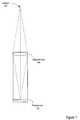
- Figure 1illustrates an exemplary conventional digital camera that employs a single objective lens 104 and a photosensor 108.
- a camera lens 104is considered "fast” if the lens collects lots of light, thus making fast shutter speed possible.
- Quality fast objective lensesare desirable because they make photography in low lighting conditions possible, and also action photography possible.
- Fast general-purpose lensesare lenses with an F/number of F/1.8 or less.
- Telephoto lensesfor example for use in sports and wildlife photography, are considered fast even at F/2.8 because they are much harder to build at lower F/numbers.
- Even point-and-shoot camerasneed relatively fast lenses if they are to be used in low light conditions in places where flash is inappropriate.
- quality fast lensesare hard to design and to build, and thus tend to be expensive.
- high precision lens elementsare needed. Also, those lens elements are bulky, making high-quality fast lenses big and heavy. The fact that high-quality objective lenses are typically actually a series of two or more individual lenses in series to provide correction for aberrations in individual lenses adds to both the bulk and the expense of the objective lenses.
- a conventional cameradoes not capture information about the location on the aperture where different light rays enter the camera.
- a conventional digital cameracaptures a two-dimensional (2D) image representing a total amount of light that strikes each point on a photosensor 108 within the camera.
- this 2D imagecontains no information about the directional distribution of the light that strikes the photosensor 108.
- Directional information at the pixelscorresponds to locational information at the aperture.
- light-field camerassample the four-dimensional (4D) optical phase space or light-field and in doing so capture information about the directional distribution of the light rays.
- This information captured by light-field camerasmay be referred to as the light-field, the plenoptic function, or radiance.
- Radiancedescribes both spatial and angular information, and is defined as density of energy per unit of area per unit of stereo angle (in radians).
- a light-field cameracaptures radiance; therefore, images originally taken out-of-focus may be refocused, noise may be reduced, viewpoints may be changed, and other light-field effects may be achieved.
- Light-field camerashave been designed based on modifications to conventional digital cameras.
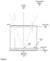
- Figure 2illustrates an exemplary prior art light-field camera, or camera array, which employs an array of two or more objective lenses 110. Each objective lens focuses on a particular region of photosensor 108, or alternatively on a separate photosensor 108.
- This light-field cameramay be viewed as a combination of two or more conventional cameras that each simultaneously records an image of subject 102 on a particular region of photosensor 108 or alternatively on a particular photosensor 108. The captured images may then be combined to form one image.
- Figure 3illustrates an exemplary prior art plenoptic camera, another type of light-field camera, that employs a single objective lens and a microlens or lenslet array 106 that includes, for example, about 100,000 lenslets that is placed a small distance ( ⁇ 0.5 mm) from a photosensor 108, e.g. a charge-coupled device (CCD).
- the raw image captured with a plenoptic camera 100is made up of an array of smal images, typically circular, of the main camera lens 108. These small images may be referred to as microimages.
- the lenslet array 106enables the plenoptic camera 100 to capture the light-field, i.e. to record not only image intensity, but also the distribution of intensity in different directions at each point.
- Each lensletsplits a beam coming to it from the main lens 104 into rays coming from different "pinhole" locations on the aperture of the main lens 108. Each of these rays is recorded as a pixel on photosensor 108, and the pixels under each lenslet collectively form an n-pixel image.
- This n-pixel area under each lensletmay be referred to as a macropixel, and the camera 100 generates a microimage at each macropixel.
- the plenoptic photograph captured by a camera 100 with, for example, 100,000 lensletswill contain 100,000 macropixels, and thus generate 100,000 microimages of subject 102.
- a conventional picture of subject 102may be created from the microimages of subject 102 captured at the macropixels.
- images originally taken out-of-focusmay be refocused, noise may be reduced, and other light-field effects may be achieved.
- Document US5946077describes a method and apparatus for the production of three dimensional images utilizing a multi-lens camera and a multi-lens enlarger configured according to a standard of arrangements.
- the number of lenses used in the camera and the enlargeris selected to be greater than the resolution capabilities of the human eye and the lenticular print system.
- the width of a zone of the lineiform imageis determined by the distance between two adjacent images on the focal plane of the lenticular screen of a point projected from a distance at or beyond the distance limit through adjacent projecting apertures of the enlarger.
- the projecting apertures of the enlargerare linearly arrayed and equally spaced within the accepting angle corresponding to the distance limit to construct a lineiform image without gaps between zones and without gaps between lines. Accordingly, a three dimensional image having orthoscopic effect, without stroboscopic effect, is produced in a one-step imaging and one-step composing process.
- lenticularefers to a single optical lens of a lenticular screen and that it is important to recognize that each lenticula is, in effect, a bead or ridge extending the entire length of the lenticular screen.
- Document WO2007115281describes a plenoptic camera which captures information about the direction distribution of light rays entering the camera.
- This plenoptic cameraincludes a main lens, which receives light from objects in an object field, and directs the received light onto an image plane of the camera. It also includes a photodetector array at the image plane of the camera, which captures the received light to produce an image.
- the plenoptic cameraincludes an array of optical elements located between the object field and the main lens. Each optical element in this array receives light from the object field from a different angle than the other optical elements in the array, and directs a different view of the object field into the main lens.
- the photodetector arrayreceives a different view of the object field from each optical element in the array.
- Document WO02/078324describes a digital stereo camera using a single sensor array to take both left and right images for stereo (three-dimensional) image capture.
- a micro-lens arrayis used to focus, at a first instant in time, light ("left light") from a left lens system onto a sensor array for left image capture. Then, the micro-lens array is moved to focus light (“right light”) from a right lens system onto the sensor array for right image capture.
- a portion of the left light (the portion having a first polarized direction) and a portion of the right light (the portion having a second polarized direction)are directed to a sensor array; the second polarized direction being orthogonal to the first polarized direction.;
- a polarization filteris used to allow the left light (having the first polarized direction) to pass toward the sensor array while preventing the right light (having the second polarized direction) from reaching the sensor array.
- polarization direction of the polarization filteris switched to allow only the right light (having the second polarized direction) to reach the sensor array.
- the two lens arraysinclude a lenslet array in front of the photosensor, and a second array of two or more separate lenses or microlenses that perform as the objective lens.
- the lens array that replaces the conventional camera objective lensis much thinner and lighter when compared to conventional camera objective lenses, and in addition may be produced and provided at less expense than conventional fast objective lenses while producing, via post-processing of the raw captured image information, final images that are similar to or better in quality to those produced by fast, expensive conventional objective lenses.
- the final image that is produced after appropriate processing of raw image data captured with embodiments of the computational cameramay, for example, be equivalent to an image captured with a lens with an F/number of F/1 or even lower.
- embodiments of the computational cameraare true light-field cameras that capture the light-field (radiance), recording not only image intensity, but also the distribution of intensity in different directions at each point.
- each of N objective lenses in an objective lens arraycaptures light from a subject, where N ⁇ 2.
- Each of M lenslets in a lenslet arraycaptures light from each objective lens, where M ⁇ 2.
- Mwill also be ⁇ N, typically > N.
- Each lenslet in the lenslet arrayseparates the captured light to generate N microimages corresponding to the N obj ective lenses on the region of the photosensor under the lenslet.
- N * Mmicroimages projected onto and captured by the photosensor.
- the (N * M) microimagesmay then be processed by an algorithm implemented in hardware, software, or a combination thereof in accordance with the geometry of the objective lenses to align the (N * M) microimages to generate a final image.
- the algorithm for processing the raw image datamay be implemented within the computational camera itself or alternatively in a separate device or computer system to which captured image information may be transferred from the computational camera.
- embodimentsmay also incorporate one or more algorithms implemented in hardware and/or software that perform various functions on the image data in accordance with radiance information captured by the computational camera, such as automatic refocusing of an out-of-focus image.
- Embodimentsmay provide a fast, light, and relatively inexpensive camera, when compared to conventional cameras, that is based on an optical system that incorporates two arrays of lenses.
- the two lens arraysinclude a lenslet array in front of a photosensor such as a Charge-Coupled Device (CCD), and a second array of two or more separate lenses or microlenses that perform as the objective lens.
- CCDCharge-Coupled Device
- the lens array that replaces the conventional camera objective lensis much thinner and lighter when compared to conventional camera objective lenses, particularly fast objective lenses (lenses with low F/numbers), and in addition may be produced and provided at less expense than conventional fast objective lenses while producing, via post-processing of the raw captured image information, final images that are similar to or better in quality to those produced by cameras employing fast, expensive conventional objective lenses.
- the final image that is produced after appropriate processing of raw image data captured with embodiments of the computational cameramay be equivalent to an image captured with an objective lens at F/1 or even lower.
- embodiments of the computational cameraare true light-field cameras that capture the light-field (radiance), recording not only image intensity, but also the distribution of intensity in different directions at each point.
- embodiments of the computational cameramay be configured to be faster (have lower F/numbers) and to provide higher resolution than conventional light-field cameras, including conventional plenoptic cameras, such as the exemplary conventional light-field cameras illustrated in Figures 2 and 3 .
- a method to make a faster camerais to make the main lens aperture larger in order to capture more light.
- a method to increase resolution in a digital camerais to use more pixels in the photosensor (e.g., more pixels in a CCD).
- Both of these objectivesmay be achieved by using an objective lens array that includes more than two objective lenses and a second array of lenslets between the objective lens array and the photosensor, as is described herein for various embodiments of a computational camera.
- Figure 4illustrates an exemplary computational camera including three lenses as objective lenses in an objective lens array and a lenslet array between the objective lens array and a photosensor, according to one embodiment. The embodiment illustrated in Figure 4 uses three objective lenses arranged linearly.
- each lenslet 222 in lenslet array 220have an F/number of 4 (F/4).
- Each lenslet 222 in exemplary lenslet array 220receives light from each objective lens 232 in objective lens array 230.
- lenslet 222nis shown receiving light from subject 250 from each objective lens 232.
- Lenslet 222nrefracts and focuses the light from each objective lens 232 onto one or more pixels in a region, or macropixel, of photosensor 210 under the lenslet 222n.
- microimages 224each corresponding to one of the objective lenses 232, being captured at photosensor 210 in a region or macropixel under lenslet 222n.
- the three objective lenses 232create, under each lenslet 222, three microimages 224.
- These microimages 224generally match the shape of the objective lenses 232; for example, these microimages 224 are circular if the objective lenses 232 are circular.
- the microimages 224are positioned relative to one another according to the positioning of the objective lenses 232.
- Each objective lens 232creates its own image centered under the lens.
- multiple objective lenses 232create, on lenslet array 220, multiple images that may overlap one another, creating what may be referred to as a "ghosting" artifact.
- the ghosting artifactmay be corrected according to an algorithm implemented in hardware, software, or a combination thereof.
- the algorithmmay correct for the ghosting artifact created by the exemplary computational camera 200 of Figure 4 by shifting the left and right microimages 224 under each lenslet 222 to the right and left, respectively, in accordance with the geometry of the objective lens array, for example in accordance with the distance between the objective lenses 232.
- lenslets 222 in lenslet array 220 of the exemplary computational camera 200 illustrated in Figure 4may have an F/number of F/4.
- the conventional plenoptic camera 100 illustrated in Figure 3has a single main (objective) lens 104 at the same F/number as for the lenslets in lenslet array 106 (e.g., F/4)
- the computational camera 200 illustrated in Figure 4uses three smaller objective lenses 232 each with an F/number of F/20.
- the individual microimages 224 of the objective lenses 232 created on photosensor 210 of computational camera 200are smaller than the single microimage 112 created by plenoptic camera 100 of Figure 3 .
- microimages 224 created by computational camera 200collect all the light that falls on each lenslet 222, the microimages 224 are brighter than microimage 112 created by plenoptic camera 100 since the light is focused on a smaller area.
- the diameter of the microimage 224 area in computational camera 200is smaller by a factor that is the ratio of the F/numbers of lenslets 222 and main lenses 232 of the computational camera 200.
- a very fast camera that operates at the F/number of the lenslets 222may be effectively created.
- each region under each lenslet 222includes three microimages 224 coming from the three objective lenses 232.
- each individual microimage 224is similar in size to the single microimage 112 of a plenoptic camera 100 as illustrated in Figure 3 with lenses of similar F/numbers to those in exemplary computational camera 200 of Figure 4 , collectively the three microimages 224 combine to form a microimage that is greater in area (i.e., covers more pixels) than does the single microimage 112 of plenoptic camera 100.
- computational camera 200achieves the objective of better utilization of the resolution of the digital camera by using more of the pixels in the photosensor 210.
- embodimentsmay include arrays of more than three objective lenses 232.
- other embodimentsmay use a 2x2 array 230 of objective lenses 232 for a total of four objective lenses 232, a 3x2 array 230 of objective lenses 232 for a total of six objective lenses 232, a 3x3 array 230 of objective lenses 232 for a total of nine objective lenses 232, and so on, thus using even more, or even virtually all, of the pixels on the photosensor 210.
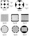
- Figures 8A and 8B and Figures 9A through 9Fillustrate several exemplary embodiments of objective lens array 230 with varying numbers and configurations of objective lenses 232.
- Figures 6A and 6Billustrate an exemplary embodiment that uses a 20x20 array 230 of objective lenses 232, for a total of 400 objective lenses 232.
- An embodiment that uses two objective lenses 232is also possible. While embodiments are generally described herein as using more or less square or rectangular arrays 230 of objective lenses 232, it is to be noted that embodiments that use other arrangements of objective lenses, for example circular, triangular, pentagonal, hexagonal, and octagonal arrays 230 are also possible, as well as arrays of other regular or irregular geometric shapes.
- one embodimentmay use a circular array 230 that includes, for example, seven objective lenses 232 with one lens in the middle and the other six arranged around the middle lens.
- each of N objective lenses 232 in an objective lens array 230refracts light from a subject, where N >2.
- Each of M lenslets 222 in a lenslet array 220refracts light from each objective lens 232, M>2.
- Mwill also be >N.
- Each lenslet 222separates the light to generate N microimages corresponding to the N objective lenses 232 on a region of the photosensor 210 under the lenslet 222.
- An algorithm for the alignment of microimages 224 by shifting the microimages according to the distance between objective lenses 232is made possible by the lenslets 222 in lenslet array 220 which each separate rays coming from different objective lenses 232 according to their direction to thus create separate microimages 224 corresponding to each objective lens on photosensor 210.
- the "ghosting" artifact due to the multiple objective lenses of the computational camera 200may be corrected according to an algorithm implemented in hardware, software, or a combination thereof.
- the algorithmmay correct the ghosting effect by shifting the left and right microimages 224 to the right and left, respectively, in accordance with the distance between the objective lenses 232.
- the right microimage 224 under lenslet 222nis shifted 38 lenslets 222 to the left and replaces the right microimage 224 created under that lenslet 222
- the left microimage 224 under lenslet 222nis shifted 38 lenslets 222 to the right and replaces the left microimage 224 created under that lenslet 222.
- Variations of this algorithmmay be used to fix or align the microimages 224 created with other configurations of objective lenses 232, for example the microimages created in an embodiment that uses a 3x3 array 230 of nine objective lenses 232.
- the above-described algorithm for aligning the microimages 224 created in computational camera 200, and/or other image processing algorithms for application to image date captured by embodiments of computational camera 200may be implemented in hardware, software, or a combination thereof.
- the algorithm, and/or other image processing algorithms for application to image date captured by embodiments of computational camera 200may be implemented in hardware, software, or a combination thereof in embodiments of computational camera 200, in a computer system or other device to which raw image date from computational camera 200 may be downloaded or otherwise transferred, or in both.
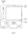
- Figure 5illustrates an exemplary embodiment of computational camera 200 with various other elements integrated in the camera 200.
- the objective lens array 230, the lenslet array 220, and the photosensor 210may be configured to fit within a volume that is no less than 10x10x10 millimeters and no more than 200x200x200 millimeters.
- an algorithm for aligning the microimages 224 created in computational camera 200, and/or other image processing algorithms for application to image date captured by embodiments of computational camera 200may be implemented in captured data processing module 260.
- Captured data processing module 260may be implemented in hardware, software, or a combination thereof.
- Embodiments of computational camera 200may include other elements.
- a computational camera 200may include a shutter 314.
- Shutter 314may be located in front of or behind objective lens array 230.
- a computational camera 200may include one or more processors 300.
- a computational camera 200may include a power supply or power source 304, such as one or more batteries.
- a computational camera 200may include a memory storage device or system 302 for storing captured image date and/or captured final images or other information such as software.
- the memory 302may be a removable storage device such as a memory stick.
- a computational camera 200may include a screen 306 (e.g., an LCD screen) for viewing scenes in front of the camera prior to capture and/or for viewing previously captured images. The screen 306 may also be used to display one or more menus or other information to the user.
- a computational camera 200may include one or more I/O interfaces 312, such as FireWire or Universal Serial Bus (USB) interfaces, for transferring information, e.g.
- I/O interfaces 312such as FireWire or Universal Serial Bus (USB) interfaces
- a computational camera 200may include one or more controls 310, for example controls for controlling optical aspects of the camera 200 such as shutter speed, one or more controls for viewing and otherwise managing and manipulating captured images stored in a memory on the camera, etc.
- a computational camera 200may include a shutter release 308 that is activated to capture an image of a subject.
- embodiments of a computational camera 200 as described hereinmay include, in addition to the two arrays of lenses 220 and 230 and photosensor 210, any other type of elements and features commonly found in digital cameras or other cameras including light-field and plenoptic cameras, and may also include additional elements and features.
- Figures 6A and 6Billustrate an exemplary computational camera including a 20 x 20 array of objective lenses and a lenslet array according to one embodiment.
- the embodiment of computational camera 200 illustrated in Figures 6A and 6Buses a 20 x 20 objective lens array 230 that includes a total of 400 objective lenses 232 arranged, for example, in a square or rectangle.
- computational camera 200 of Figures 6A and 6Bmay be implemented as a camera that is more or less cubical, with dimensions of, or approximately of, 40x40x40 millimeters (mm). Other embodiments may use other dimensions and/or configurations than the exemplary cubic or approximately cubic configuration.
- the computational camera 200may include a shutter similar to shutters used in conventional cameras, which may be located in front of or behind objective lens array 230, that may be used to capture timed exposures on photosensor 210.
- the lenslets 212 in lenslet array 210are of the diameter 20 microns (20 ⁇ m).
- the lenslet array 210includes 2000 x 2000 lenslets 212, or four million lenslets.
- the final imagewill have a resolution of 20 microns (20 ⁇ m), or 50 lines per mm. This resolution is better than that of conventional camera lenses at low F/number.
- the lenslets 212 in lenslet array 210have a focal length of 20 microns (20 ⁇ m).
- the lenslets 212have an F/number of F/1.
- essentially any lensletsis diffraction limited.
- (1.22 * ⁇ * F)yields a diffraction spot of 0.6 microns.
- the objective lens array 230 that replaces the single main camera (objective) lens, for example the main (objective) lens in a conventional SLR camera,is much lighter, and may be as thin as, for example, 1 mm, while the image is of equal or even better quality. Furthermore, the manufacturing cost of the objective lens array 230 may be less than that of conventional high-quality single-lens-type objective lenses. High performance conventional camera objective lenses that may cost several thousand dollars have reached their optimal solution and are not likely to become any less expensive.
- embodiments of the computational camera 200 as described hereinmaybe less expensive to produce than conventional single objective lens cameras while producing images of equal or better quality, and in addition may provide very fast camera speeds (i.e., with low F/numbers, F/1 or even lower) at much lower cost and size/weight than is possible with conventional single-lens solutions.
- embodiments of the computational camera 200 described hereinare true light-field cameras that capture the light-field, recording not only image intensity, but also the distribution of intensity in different directions at each point.
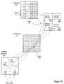
- Figures 7A and 7Billustrate the capturing and processing of a digital image exemplary computational camera including a 2 x 2 array of objective lenses and a lenslet array according to one embodiment.
- the configuration of the embodiment of computational camera 200 illustrated in Figures 7A and 7Bis relatively simple to aid in illustrating and describing the capturing and processing of a digital image using camera 200.
- Camera 200 in this exampleuses a 2 x 2 objective lens array 230 that provides a total of four objective lenses 232 that may be arranged, for example, in a square or rectangle.
- the exemplary lenslet array 220 in Figure 7Aincludes 10 x 10, or 100, lenslets 222.
- the distance between the objective lenses 232would be five lenslets.
- each objective lens 232In capturing an image of subject 250, light from subject 250 is collected by each objective lens 232. Light from each objective lens 232 is collected by each lenslet 222 in lenslet array 220. The lenslets 222 in lenslet array 220 each separate rays coming from the objective lenses 232 according to their direction to thus create separate microimages corresponding to each objective lens 232 on photosensor 210.
- a region 216n of photosensor 210 which corresponds to lenslet 222nis expanded to show that light from the four objective lenses 232 is separated into four microimages on the region 216n.
- each objective lens 232corresponds to one subregion of region 216n. Each subregion may include one or more pixels. Thus, region 216n includes at least four pixels.
- the raw image data captured by photosensor 210may be processed by captured data processing module 260 to generate a digital image 270 of subject 250.
- This processingmay include, but is not limited to, shifting at least some of the data captured at the subregions of regions 216 in accordance with the geometry of, e.g. the distance between, the objective lenses 232 to correct for "ghosting," as previously described.
- the distance between the objective lenses 232is five lenslets; therefore, the captured image data for a subregion may be shifted five regions to the right or left, or five regions up or down.
- image data for a subregion of a region 216may be replaced by data shifted from another subregion of a different region.
- the algorithmmay match and combine image data captured on different pixels on different regions under different lenslets 220.
- FIGs 8A and 8Billustrate exemplary objective lens arrays 230.
- four objective lenses 232are shown mounted in a square housing 234.
- four objective lenses 232are shown mounted in a circular housing 234.
- housing 234may be opaque to light so that light from a subject only reaches the lenslet array 220 through objective lenses 232.
- Housing 234may be made of a metal, alloy, plastic, composite material, or in general of any suitable substance or combination of substances. Housing 234 may be integrated with a computational camera 200 or may be a removable and replaceable/interchangeable component or module. Further, lenses 232 may be integrated with housing 234 or may be removable and replaceable.
- Housing 234, if a removable and replaceable/interchangeable component or module,may include one or more mechanisms for mounting the objective lens array 232 to a compatible camera housing.
- housing 234may be threaded, and/or may have one or more holes, screws, bolts, or other mechanism or mechanisms for mounting the objective lens array 232 to a compatible camera housing.
- objective lens array 230may have an integrated shutter. In other embodiments, the shutter may be a separate component or may be integrated with the camera housing.
- Figures 9A-9Fillustrate various exemplary configurations for objective lens array 230.
- Figure 9Aillustrates a square objective lens array 230 housing that holds a 10 x 10 array of objective lenses 232.
- Figure 9Billustrates an objective lens array 232 housing that is configured as a square with rounded corners. The array of lenses 232 consists of 45 lenses that are "packed" into a roughly rectangular geometry in the housing 234 to minimize space between the lenses 232, with four rows of six lenses and three rows of seven lenses.
- Figure 9Cillustrates a square objective lens array 230 housing with an 8 x 10 rectangular array of objective lenses 232.
- Figures 9D-9Fillustrate circular objective lens array 230 housings with various configurations of lens arrays mounted in the housings 234.
- the objective lenses 232may be arranged in the objective lens array 230 in different shapes.
- the shapesmay generally be, but are not necessarily, regular geometric shapes.
- the regular geometric shapein at least some embodiments may be a polygon.
- the number of objective lenses 232may be less than or equal to 10,000, although embodiments that use more than 10,000 objective lenses 232 are possible.
- the objective lens arrays 230 illustrated in Figures 8A-8B, and 9A-9Fare exemplary, and are not intended to be limiting. Objective lens arrays 230 of various dimensions and configurations are possible and contemplated. Furthermore, various dimensions and configurations of lenslet arrays 220 are possible and contemplated. Note that at least part of the above illustrations and discussions of exemplary objective lens arrays 230 in regard to Figures 8A-8B, and 9A-9F may be applied to the configuration of lenslet arrays 220, although lenslet arrays 220 may tend to have smaller and more numerous lenslets 222 than there are lenses 232 in objective lens arrays 230 used with the lenslet arrays 220.
- lenslet array 220may be integrated with the computational camera 200, may be a removable and replaceable/interchangeable component or module, or may be integrated with the photosensor 210. In embodiments that include a lenslet array 220 integrated with the photosensor 210, the lenslet array/photosensor component may be integrated with the computational camera 200 or may be a removable and replaceable/interchangeable module.
- the objective lens array 230, the lenslet array 220, and the photosensor 210may be configured to fit within a volume that is no less than 10x10x10 millimeters and no more than 200x200x200 millimeters.
- the objective lenses 232 in objective lens array 230may have an F/number between F/10 and F/100, inclusive, and the lenslets 220 in lenslet array 220 may have an F/number between F/0.7 and F/2, inclusive.
- Exemplary physical characteristics for objective lens arrays 230, lenslet arrays 220, and photosensors 210have been described herein. Furthermore, exemplary physical and optical characteristics (e.g., focal length, F/numbers, dimensions, etc.) for both objective lenses 232 and lenslets 222, alone and in combination, have been described herein. It is to be understood that these physical and optical characteristics are exemplary, and are not intended to be limiting.
- Figures 6B, 7A, 8A-8B, and 9A-9Fshow the lenses 232 in objective lens array 230 and the lenslets 222 in lenslet array 220 as circular lenses, other shapes of lenses 232 and/or lenslets 222 than circular may be used.
- square lenses and/or lensletsmay be used in embodiments, or square lenses with rounded corners may be used.
- triangular, rectangular, hexagonal, octagonal, etc. lensesmay be used.
- the lenses 232 and lenslets 222are generally illustrated in the drawings as conventional lenses with two convex surfaces, other configurations of lenses may be used, for example lenses with one convex surface and one flat surface, or lenses with one convex surface and one concave surface.
- FIG 10is a flowchart describing the operation of a computational camera according to one embodiment.
- each of N objective lenses in an objective lens arrayrefracts light from a subject, where N ⁇ 2.
- each of M lenslets in a lenslet arrayrefracts light from each objective lens, where M ⁇ 2.
- Mwill also be ⁇ N, typically > N.
- each lensletseparates the light to generate N microimages corresponding to the N objective lenses on the region of the photosensor under the lenslet.
- the (N * M) microimagesare processed by an algorithm implemented in hardware, software, or a combination thereof in accordance with the geometry of the objective lenses to generate a final image.
- the algorithm for processing the raw image datamay be implemented within the computational camera itself or alternatively in a separate device or computer system to which captured image information may be transferred from the computational camera, for example via an I/O interface such as FireWire or USB or via memory transfer, e.g. via a memory stick or other removable memory device.
- embodimentsmay also incorporate one or more algorithms implemented in hardware and/or software that perform various functions on the image data in accordance with radiance information captured by the computational camera, such as automatic refocusing of an out-of-focus image.
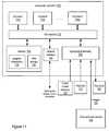
- Computer system 700includes one or more processors 710 coupled to a system memory 720 via an input/output (I/O) interface 730.
- Computer system 700further includes a network interface 740 coupled to I/O interface 730, and one or more input/output devices 750, such as cursor control device 760, keyboard 770, audio device 790, and display(s) 780.
- embodimentsmay be implemented using a single instance of computer system 700, while in other embodiments multiple such systems, or multiple nodes making up computer system 700, may be configured to host different portions or instances of embodiments.
- some elementsmay be implemented via one or more nodes of computer system 700 that are distinct from those nodes implementing other elements.
- computer system 700may be a uniprocessor system including one processor 710, or a multiprocessor system including several processors 710 (e.g., two, four, eight, or another suitable number).
- processors 710may be any suitable processor capable of executing instructions.
- processors 710may be general-purpose or embedded processors implementing any of a variety of instruction set architectures (ISAs), such as the x86, PowerPC, SPARC, or MIPS ISAs, or any other suitable ISA.
- ISAsinstruction set architectures
- each of processors 710may commonly, but not necessarily, implement the same ISA.
- System memory 720may be configured to store program instructions and/or data accessible by processor 710.
- system memory 720may be implemented using any suitable memory technology, such as static random access memory (SRAM), synchronous dynamic RAM (SDRAM), nonvolatile/Flash-type memory, or any other type of memory.
- SRAMstatic random access memory
- SDRAMsynchronous dynamic RAM
- program instructions and data implementing desired functionssuch as those described above for software for processing image data captured by various embodiments of a computational camera 200 as described herein, are shown stored within system memory 720 as program instructions 725 and data storage 735, respectively.
- program instructions and/or datamay be received, sent or stored upon different types of computer-accessible media or on similar media separate from system memory 720 or computer system 700.
- a computer-accessible mediummay include storage media or memory media such as magnetic or optical media, e.g., disk or CD/DVD-ROM coupled to computer system 700 via I/O interface 730.
- Program instructions and data stored via a computer-accessible mediummay be transmitted by transmission media or signals such as electrical, electromagnetic, or digital signals, which may be conveyed via a communication medium such as a network and/or a wireless link, such as may be implemented via network interface 740.
- I/O interface 730may be configured to coordinate I/O traffic between processor 710, system memory 720, and any peripheral devices in the device, including network interface 740 or other peripheral interfaces, such as input/output devices 750.
- I/O interface 730may perform any necessary protocol, timing or other data transformations to convert data signals from one component (e.g., system memory 720) into a format suitable for use by another component (e.g., processor 710).
- I/O interface 730may include support for devices attached through various types of peripheral buses, such as a variant of the Peripheral Component Interconnect (PCI) bus standard or the Universal Serial Bus (USB) standard, for example.
- PCIPeripheral Component Interconnect
- USBUniversal Serial Bus
- I/O interface 730may be split into two or more separate components, such as a north bridge and a south bridge, for example.
- some or all of the functionality of I/O interface 730, such as an interface to system memory 720,may be incorporated directly into processor 710.
- Network interface 740may be configured to allow data to be exchanged between computer system 700 and other devices attached to a network, such as other computer systems, or between nodes of computer system 700.
- network interface 740may support communication via wired or wireless general data networks, such as any suitable type of Ethernet network, for example; via telecommunications/telephony networks such as analog voice networks or digital fiber communications networks; via storage area networks such as Fibre Channel SANs, or via any other suitable type of network and/or protocol.
- Input/output devices 750may include input from a computational camera 200 for receiving image data captured by embodiments the computational camera 200 as described herein.
- Input/output devices 750may, in some embodiments, include one or more display terminals, keyboards, keypads, touchpads, scanning devices, voice or optical recognition devices, or any other devices suitable for entering or retrieving data by one or more computer system 700.
- Multiple input/output devices 750may be present in computer system 700 or may be distributed on various nodes of computer system 700.
- similar input/output devicesmay be separate from computer system 700 and may interact with one or more nodes of computer system 700 through a wired or wireless connection, such as over network interface 740.
- memory 720may include program instructions 725, configured to implement software, including but not limited to software for processing image data captured by various embodiments of a computational camera as described herein, and data storage 735, comprising various data accessible by program instructions 725.
- Data storage 735may include data that may be used in some embodiments. In other embodiments, different software elements and data may be included.
- computer system 700is merely illustrative and is not intended to limit the scope of the computational camera 200 as described herein.
- the computer system and devicesmay include any combination of hardware or software that can perform the indicated functions, including but not limited to computers, network devices, internet appliances, PDAs, etc.
- Computer system 700may also be connected to other devices that are not illustrated, or instead may operate as a stand-alone system.
- the functionality provided by the illustrated componentsmay in some embodiments be combined in fewer components or distributed in additional components.
- the functionality of some of the illustrated componentsmay not be provided and/or other additional functionality may be available.
- instructions stored on a computer-accessible medium separate from computer system 700may be transmitted to computer system 700 via transmission media or signals such as electrical, electromagnetic, or digital signals, conveyed via a communication medium such as a network and/or a wireless link.
- Various embodimentsmay further include receiving, sending or storing instructions and/or data implemented in accordance with the foregoing description upon a computer-accessible medium. Accordingly, the present invention may be practiced with other computer system configurations.
- a computer-accessible mediummay include storage media or memory media such as magnetic or optical media, e.g., disk or DVD/CD-ROM, volatile or non-volatile media such as RAM (e.g. SDRAM, DDR, RDRAM, SRAM, etc.), ROM, etc.
- storage media or memory mediasuch as magnetic or optical media, e.g., disk or DVD/CD-ROM, volatile or non-volatile media such as RAM (e.g. SDRAM, DDR, RDRAM, SRAM, etc.), ROM, etc.
- transmission media or signalssuch as electrical, electromagnetic, or digital signals, conveyed via a communication medium such as network and/or a wireless link.
Landscapes
- Physics & Mathematics (AREA)
- General Physics & Mathematics (AREA)
- Optics & Photonics (AREA)
- Studio Devices (AREA)
- Image Processing (AREA)
Description
- This invention relates to cameras, and more specifically to digital cameras and light-field cameras.
Figure 1 illustrates an exemplary conventional digital camera that employs a singleobjective lens 104 and aphotosensor 108. Acamera lens 104 is considered "fast" if the lens collects lots of light, thus making fast shutter speed possible. The F/number of a lens is a measure of how much light can be collected by the lens, where:
- Quality fast objective lenses are desirable because they make photography in low lighting conditions possible, and also action photography possible. Fast general-purpose lenses are lenses with an F/number of F/1.8 or less. Telephoto lenses, for example for use in sports and wildlife photography, are considered fast even at F/2.8 because they are much harder to build at lower F/numbers. Even point-and-shoot cameras need relatively fast lenses if they are to be used in low light conditions in places where flash is inappropriate. However, quality fast lenses are hard to design and to build, and thus tend to be expensive. There are optical solutions to the problem of building fast lenses. However, those solutions get very expensive at low F/numbers due to the large angle of refraction far from optical axis at low F/numbers, which means correction for aberrations becomes difficult. Multiple high precision lens elements are needed. Also, those lens elements are bulky, making high-quality fast lenses big and heavy. The fact that high-quality objective lenses are typically actually a series of two or more individual lenses in series to provide correction for aberrations in individual lenses adds to both the bulk and the expense of the objective lenses.
- Another approach is to increase photon efficiency of the photosensor (e.g., a charge-coupled device (CCD)). However, the industry has already reached near-optimal efficiency at acceptable prices. Also, at current efficiencies of 50% or more, achieving significant improvements is difficult. Even in theory efficiency of photosensors cannot improve more than two times better, as efficiency above 100% obviously cannot be reached.
- Conventional cameras, as illustrated in
Figure 1 , fail to capture a large amount of optical information. In particular, a conventional camera does not capture information about the location on the aperture where different light rays enter the camera. During operation, a conventional digital camera captures a two-dimensional (2D) image representing a total amount of light that strikes each point on aphotosensor 108 within the camera. However, this 2D image contains no information about the directional distribution of the light that strikes thephotosensor 108. Directional information at the pixels corresponds to locational information at the aperture. - In contrast, light-field cameras sample the four-dimensional (4D) optical phase space or light-field and in doing so capture information about the directional distribution of the light rays. This information captured by light-field cameras may be referred to as the light-field, the plenoptic function, or radiance. Radiance describes both spatial and angular information, and is defined as density of energy per unit of area per unit of stereo angle (in radians). A light-field camera captures radiance; therefore, images originally taken out-of-focus may be refocused, noise may be reduced, viewpoints may be changed, and other light-field effects may be achieved. Light-field cameras have been designed based on modifications to conventional digital cameras.
Figure 2 illustrates an exemplary prior art light-field camera, or camera array, which employs an array of two or moreobjective lenses 110. Each objective lens focuses on a particular region ofphotosensor 108, or alternatively on aseparate photosensor 108. This light-field camera may be viewed as a combination of two or more conventional cameras that each simultaneously records an image ofsubject 102 on a particular region ofphotosensor 108 or alternatively on aparticular photosensor 108. The captured images may then be combined to form one image.Figure 3 illustrates an exemplary prior art plenoptic camera, another type of light-field camera, that employs a single objective lens and a microlens orlenslet array 106 that includes, for example, about 100,000 lenslets that is placed a small distance (∼0.5 mm) from aphotosensor 108, e.g. a charge-coupled device (CCD). The raw image captured with aplenoptic camera 100 is made up of an array of smal images, typically circular, of themain camera lens 108. These small images may be referred to as microimages. Thelenslet array 106 enables theplenoptic camera 100 to capture the light-field, i.e. to record not only image intensity, but also the distribution of intensity in different directions at each point. Each lenslet splits a beam coming to it from themain lens 104 into rays coming from different "pinhole" locations on the aperture of themain lens 108. Each of these rays is recorded as a pixel onphotosensor 108, and the pixels under each lenslet collectively form an n-pixel image. This n-pixel area under each lenslet may be referred to as a macropixel, and thecamera 100 generates a microimage at each macropixel. The plenoptic photograph captured by acamera 100 with, for example, 100,000 lenslets will contain 100,000 macropixels, and thus generate 100,000 microimages ofsubject 102. By appropriately selecting a pixel from each macropixel, a conventional picture ofsubject 102 may be created from the microimages ofsubject 102 captured at the macropixels. Moreover, by mixing such images appropriately, images originally taken out-of-focus may be refocused, noise may be reduced, and other light-field effects may be achieved.- Document
US5946077 describes a method and apparatus for the production of three dimensional images utilizing a multi-lens camera and a multi-lens enlarger configured according to a standard of arrangements. The number of lenses used in the camera and the enlarger is selected to be greater than the resolution capabilities of the human eye and the lenticular print system. The width of a zone of the lineiform image is determined by the distance between two adjacent images on the focal plane of the lenticular screen of a point projected from a distance at or beyond the distance limit through adjacent projecting apertures of the enlarger. The projecting apertures of the enlarger are linearly arrayed and equally spaced within the accepting angle corresponding to the distance limit to construct a lineiform image without gaps between zones and without gaps between lines. Accordingly, a three dimensional image having orthoscopic effect, without stroboscopic effect, is produced in a one-step imaging and one-step composing process. This document clearly states that the term "lenticula" refers to a single optical lens of a lenticular screen and that it is important to recognize that each lenticula is, in effect, a bead or ridge extending the entire length of the lenticular screen. - Document
WO2007115281 describes a plenoptic camera which captures information about the direction distribution of light rays entering the camera. This plenoptic camera includes a main lens, which receives light from objects in an object field, and directs the received light onto an image plane of the camera. It also includes a photodetector array at the image plane of the camera, which captures the received light to produce an image. The plenoptic camera includes an array of optical elements located between the object field and the main lens. Each optical element in this array receives light from the object field from a different angle than the other optical elements in the array, and directs a different view of the object field into the main lens. Thus, the photodetector array receives a different view of the object field from each optical element in the array. - Document
WO02/078324 - Particular aspects of the invention are set out in the appended claims.
- Various embodiments of a method and apparatus for a computational camera that incorporates two arrays of lenses are described. The two lens arrays include a lenslet array in front of the photosensor, and a second array of two or more separate lenses or microlenses that perform as the objective lens. The lens array that replaces the conventional camera objective lens is much thinner and lighter when compared to conventional camera objective lenses, and in addition may be produced and provided at less expense than conventional fast objective lenses while producing, via post-processing of the raw captured image information, final images that are similar to or better in quality to those produced by fast, expensive conventional objective lenses. The final image that is produced after appropriate processing of raw image data captured with embodiments of the computational camera may, for example, be equivalent to an image captured with a lens with an F/number of F/1 or even lower. Furthermore, embodiments of the computational camera are true light-field cameras that capture the light-field (radiance), recording not only image intensity, but also the distribution of intensity in different directions at each point.
- In embodiments of the computational camera, each of N objective lenses in an objective lens array captures light from a subject, where N ≥ 2. Each of M lenslets in a lenslet array captures light from each objective lens, where M ≥ 2. Note that, in practice, M will also be ≥ N, typically > N. Each lenslet in the lenslet array separates the captured light to generate N microimages corresponding to the N obj ective lenses on the region of the photosensor under the lenslet. Thus, there are a total of (N * M) microimages projected onto and captured by the photosensor. The (N * M) microimages may then be processed by an algorithm implemented in hardware, software, or a combination thereof in accordance with the geometry of the objective lenses to align the (N * M) microimages to generate a final image. The algorithm for processing the raw image data may be implemented within the computational camera itself or alternatively in a separate device or computer system to which captured image information may be transferred from the computational camera. In addition to an algorithm for processing the raw image data to produce a final digital image, embodiments may also incorporate one or more algorithms implemented in hardware and/or software that perform various functions on the image data in accordance with radiance information captured by the computational camera, such as automatic refocusing of an out-of-focus image.
Figure 1 illustrates an exemplary prior art digital camera that employs a single objective lens and a photosensor.Figure 2 illustrates an exemplary prior art light-field camera, or camera array, which employs an array of two or more objective lenses.Figure 3 illustrates an exemplary prior art plenoptic camera that employs a single objective lens and a microlens or lenslet array placed a small distance from a photosensor.Figure 4 illustrates an exemplary computational camera including three lenses as objective lenses and a lenslet array according to one embodiment.Figure 5 illustrates an exemplary embodiment of a computational camera with various other elements integrated in the camera.Figures 6A and6B illustrate an exemplary computational camera including a 20 x 20 array of objective lenses and a lenslet array according to one embodiment.Figures 7A and7B illustrate the capturing and processing of a digital image exemplary computational camera according to one embodiment.Figures 8A and 8B illustrate exemplaryobjective lens arrays 230.Figures 9A-9F illustrate various exemplary configurations forobjective lens array 230.Figure 10 is a flowchart describing the operation of a computational camera according to one embodiment.Figure 11 illustrates an exemplary computer system that may be used in embodiments.- While the invention is described herein by way of example for several embodiments and illustrative drawings, those skilled in the art will recognize that the invention is not limited to the embodiments or drawings described. It should be understood, that the drawings and detailed description thereto are not intended to limit the invention to the particular form disclosed, but on the contrary, the intention is to cover all modifications, equivalents and alternatives falling within the spirit and scope of the present invention as defined by the appended claims. The headings used herein are for organizational purposes only and are not meant to be used to limit the scope of the description or the claims. As used throughout this application, the word "may" is used in a permissive sense (i.e., meaning having the potential to), rather than the mandatory sense (i.e., meaning must). Similarly, the words "include", "including", and "includes" mean including, but not limited to.
- Various embodiments of a method and apparatus for a computational camera that incorporates two arrays of lenses are described. Embodiments may provide a fast, light, and relatively inexpensive camera, when compared to conventional cameras, that is based on an optical system that incorporates two arrays of lenses. The two lens arrays include a lenslet array in front of a photosensor such as a Charge-Coupled Device (CCD), and a second array of two or more separate lenses or microlenses that perform as the objective lens. The lens array that replaces the conventional camera objective lens is much thinner and lighter when compared to conventional camera objective lenses, particularly fast objective lenses (lenses with low F/numbers), and in addition may be produced and provided at less expense than conventional fast objective lenses while producing, via post-processing of the raw captured image information, final images that are similar to or better in quality to those produced by cameras employing fast, expensive conventional objective lenses. The final image that is produced after appropriate processing of raw image data captured with embodiments of the computational camera may be equivalent to an image captured with an objective lens at F/1 or even lower. Furthermore, embodiments of the computational camera are true light-field cameras that capture the light-field (radiance), recording not only image intensity, but also the distribution of intensity in different directions at each point. However, embodiments of the computational camera may be configured to be faster (have lower F/numbers) and to provide higher resolution than conventional light-field cameras, including conventional plenoptic cameras, such as the exemplary conventional light-field cameras illustrated in
Figures 2 and3 . - A method to make a faster camera is to make the main lens aperture larger in order to capture more light. A method to increase resolution in a digital camera is to use more pixels in the photosensor (e.g., more pixels in a CCD). Both of these objectives may be achieved by using an objective lens array that includes more than two objective lenses and a second array of lenslets between the objective lens array and the photosensor, as is described herein for various embodiments of a computational camera.
Figure 4 illustrates an exemplary computational camera including three lenses as objective lenses in an objective lens array and a lenslet array between the objective lens array and a photosensor, according to one embodiment. The embodiment illustrated inFigure 4 uses three objective lenses arranged linearly. In this exemplary embodiment, eachlenslet 222 inlenslet array 220 have an F/number of 4 (F/4). There are threelenses 232 in the exemplaryobjective lens array 230, each with an F/number of 20 (F/20). Eachlenslet 222 inexemplary lenslet array 220 receives light from eachobjective lens 232 inobjective lens array 230. In this example,lenslet 222n is shown receiving light from subject 250 from eachobjective lens 232.Lenslet 222n refracts and focuses the light from eachobjective lens 232 onto one or more pixels in a region, or macropixel, ofphotosensor 210 under thelenslet 222n. This results in threemicroimages 224, each corresponding to one of theobjective lenses 232, being captured atphotosensor 210 in a region or macropixel underlenslet 222n. Thus, the threeobjective lenses 232 create, under eachlenslet 222, threemicroimages 224. Thesemicroimages 224 generally match the shape of theobjective lenses 232; for example, thesemicroimages 224 are circular if theobjective lenses 232 are circular. Themicroimages 224 are positioned relative to one another according to the positioning of theobjective lenses 232. - Each
objective lens 232 creates its own image centered under the lens. Thus, multipleobjective lenses 232 create, onlenslet array 220, multiple images that may overlap one another, creating what may be referred to as a "ghosting" artifact. The ghosting artifact may be corrected according to an algorithm implemented in hardware, software, or a combination thereof. The algorithm may correct for the ghosting artifact created by the exemplarycomputational camera 200 ofFigure 4 by shifting the left andright microimages 224 under each lenslet 222 to the right and left, respectively, in accordance with the geometry of the objective lens array, for example in accordance with the distance between theobjective lenses 232. - As described above,
lenslets 222 inlenslet array 220 of the exemplarycomputational camera 200 illustrated inFigure 4 may have an F/number of F/4. However, while the conventionalplenoptic camera 100 illustrated inFigure 3 has a single main (objective)lens 104 at the same F/number as for the lenslets in lenslet array 106 (e.g., F/4), thecomputational camera 200 illustrated inFigure 4 uses three smallerobjective lenses 232 each with an F/number of F/20. As a result, theindividual microimages 224 of theobjective lenses 232 created onphotosensor 210 ofcomputational camera 200 are smaller than thesingle microimage 112 created byplenoptic camera 100 ofFigure 3 . However, since themicroimages 224 created bycomputational camera 200 collect all the light that falls on eachlenslet 222, themicroimages 224 are brighter thanmicroimage 112 created byplenoptic camera 100 since the light is focused on a smaller area. The diameter of themicroimage 224 area incomputational camera 200 is smaller by a factor that is the ratio of the F/numbers oflenslets 222 andmain lenses 232 of thecomputational camera 200. Thus, for themicroimages 224, a very fast camera that operates at the F/number of thelenslets 222 may be effectively created. - By using more than one
objective lens 232, more of the pixels in the region ofphotosensor 210 under each lenslet 222 inlenslet array 220 may be used than in a conventional plenoptic camera operating at similar F/numbers. In the exemplarycomputational camera 200 ofFigure 4 that uses threeobjective lenses 232, each region under eachlenslet 222 includes threemicroimages 224 coming from the threeobjective lenses 232. While eachindividual microimage 224 is similar in size to thesingle microimage 112 of aplenoptic camera 100 as illustrated inFigure 3 with lenses of similar F/numbers to those in exemplarycomputational camera 200 ofFigure 4 , collectively the threemicroimages 224 combine to form a microimage that is greater in area (i.e., covers more pixels) than does thesingle microimage 112 ofplenoptic camera 100. Thus,computational camera 200 achieves the objective of better utilization of the resolution of the digital camera by using more of the pixels in thephotosensor 210. - While the
exemplary camera 200 ofFigure 4 employs threeobjective lenses 232, embodiments may include arrays of more than threeobjective lenses 232. For example, other embodiments may use a2x2 array 230 ofobjective lenses 232 for a total of fourobjective lenses 232, a3x2 array 230 ofobjective lenses 232 for a total of sixobjective lenses 232, a3x3 array 230 ofobjective lenses 232 for a total of nineobjective lenses 232, and so on, thus using even more, or even virtually all, of the pixels on thephotosensor 210.Figures 8A and 8B and Figures 9A through 9F illustrate several exemplary embodiments ofobjective lens array 230 with varying numbers and configurations ofobjective lenses 232.Figures 6A and6B illustrate an exemplary embodiment that uses a20x20 array 230 ofobjective lenses 232, for a total of 400objective lenses 232. An embodiment that uses twoobjective lenses 232 is also possible. While embodiments are generally described herein as using more or less square orrectangular arrays 230 ofobjective lenses 232, it is to be noted that embodiments that use other arrangements of objective lenses, for example circular, triangular, pentagonal, hexagonal, andoctagonal arrays 230 are also possible, as well as arrays of other regular or irregular geometric shapes. For example, one embodiment may use acircular array 230 that includes, for example, sevenobjective lenses 232 with one lens in the middle and the other six arranged around the middle lens. - In embodiments of
computational camera 200, each of Nobjective lenses 232 in anobjective lens array 230 refracts light from a subject, where N >2. Each of M lenslets 222 in alenslet array 220 refracts light from eachobjective lens 232, M>2. In practice, M will also be >N. Eachlenslet 222 separates the light to generate N microimages corresponding to the Nobjective lenses 232 on a region of thephotosensor 210 under thelenslet 222. Thus, there are a total of (N * M) microimages captured on thephotosensor 210. Thephotosensor 210 includes at least P discrete pixels, where P = (N * M). - An algorithm for the alignment of
microimages 224 by shifting the microimages according to the distance betweenobjective lenses 232 is made possible by thelenslets 222 inlenslet array 220 which each separate rays coming from differentobjective lenses 232 according to their direction to thus createseparate microimages 224 corresponding to each objective lens onphotosensor 210. As mentioned above, the "ghosting" artifact due to the multiple objective lenses of thecomputational camera 200 may be corrected according to an algorithm implemented in hardware, software, or a combination thereof. In the exemplarycomputational camera 200 ofFigure 4 , the algorithm may correct the ghosting effect by shifting the left andright microimages 224 to the right and left, respectively, in accordance with the distance between theobjective lenses 232. For example, if the distance between theobjective lenses 232 is equivalent to 38lenslets 222 inlenslet array 220, theright microimage 224 underlenslet 222n is shifted 38lenslets 222 to the left and replaces theright microimage 224 created under thatlenslet 222, and theleft microimage 224 underlenslet 222n is shifted 38lenslets 222 to the right and replaces theleft microimage 224 created under thatlenslet 222. Variations of this algorithm may be used to fix or align themicroimages 224 created with other configurations ofobjective lenses 232, for example the microimages created in an embodiment that uses a3x3 array 230 of nineobjective lenses 232. - The above-described algorithm for aligning the
microimages 224 created incomputational camera 200, and/or other image processing algorithms for application to image date captured by embodiments ofcomputational camera 200, may be implemented in hardware, software, or a combination thereof. Furthermore, the algorithm, and/or other image processing algorithms for application to image date captured by embodiments ofcomputational camera 200, may be implemented in hardware, software, or a combination thereof in embodiments ofcomputational camera 200, in a computer system or other device to which raw image date fromcomputational camera 200 may be downloaded or otherwise transferred, or in both. An exemplary system in which embodiments of the algorithm, and/or other image processing algorithms for application to image date captured by embodiments ofcomputational camera 200, for example algorithms that use the captured radiance information to refocus or otherwise manipulate the captured image, may be implemented is illustrated inFigure 11 . Figure 5 illustrates an exemplary embodiment ofcomputational camera 200 with various other elements integrated in thecamera 200. In various embodiments ofcomputational camera 200, theobjective lens array 230, thelenslet array 220, and thephotosensor 210 may be configured to fit within a volume that is no less than 10x10x10 millimeters and no more than 200x200x200 millimeters.- In one embodiment, an algorithm for aligning the
microimages 224 created incomputational camera 200, and/or other image processing algorithms for application to image date captured by embodiments ofcomputational camera 200, may be implemented in captureddata processing module 260. Captureddata processing module 260 may be implemented in hardware, software, or a combination thereof. Embodiments ofcomputational camera 200 may include other elements. For example, acomputational camera 200 may include ashutter 314. Shutter 314 may be located in front of or behindobjective lens array 230. As another example, acomputational camera 200 may include one ormore processors 300. As another example, acomputational camera 200 may include a power supply orpower source 304, such as one or more batteries. As another example, acomputational camera 200 may include a memory storage device orsystem 302 for storing captured image date and/or captured final images or other information such as software. In one embodiment, thememory 302 may be a removable storage device such as a memory stick. As another example, acomputational camera 200 may include a screen 306 (e.g., an LCD screen) for viewing scenes in front of the camera prior to capture and/or for viewing previously captured images. Thescreen 306 may also be used to display one or more menus or other information to the user. As another example, acomputational camera 200 may include one or more I/O interfaces 312, such as FireWire or Universal Serial Bus (USB) interfaces, for transferring information, e.g. captured images, software updates, and so on, to and from external devices such as computer systems or even other cameras. As another example, acomputational camera 200 may include one ormore controls 310, for example controls for controlling optical aspects of thecamera 200 such as shutter speed, one or more controls for viewing and otherwise managing and manipulating captured images stored in a memory on the camera, etc. Acomputational camera 200 may include a shutter release 308 that is activated to capture an image of a subject. In general, embodiments of acomputational camera 200 as described herein may include, in addition to the two arrays oflenses photosensor 210, any other type of elements and features commonly found in digital cameras or other cameras including light-field and plenoptic cameras, and may also include additional elements and features. Figures 6A and6B illustrate an exemplary computational camera including a 20 x 20 array of objective lenses and a lenslet array according to one embodiment. The embodiment ofcomputational camera 200 illustrated inFigures 6A and6B uses a 20 x 20objective lens array 230 that includes a total of 400objective lenses 232 arranged, for example, in a square or rectangle. In one embodiment,computational camera 200 ofFigures 6A and6B may be implemented as a camera that is more or less cubical, with dimensions of, or approximately of, 40x40x40 millimeters (mm). Other embodiments may use other dimensions and/or configurations than the exemplary cubic or approximately cubic configuration. Thecomputational camera 200 may include a shutter similar to shutters used in conventional cameras, which may be located in front of or behindobjective lens array 230, that may be used to capture timed exposures onphotosensor 210.- In this embodiment of
computational camera 200, light is refracted through the20x20 array 230 of objective lenses 232 (for a total of 400 objective lenses 232). Eachobjective lens 232 has a diameter of ∼2 mm and a focal length of ∼40 mm, which corresponds to F/20. At that F/number,lenses 232 may be easily manufactured diffraction limited. Essentially, any lens is diffraction limited at high F/numbers. Furthermore, the diffraction blur circle in the case of a circular lens has a diameter (1.22 * X * F), where λ is the wavelength of light, and F is the F/number. In this exemplary case, λ = 500 nanometers (nm), and F = 20, resulting in a blur radius of 12 microns (12µm). - In this exemplary embodiment, the lenslets 212 in
lenslet array 210 are of the diameter 20 microns (20µm). Thus, thelenslet array 210 includes 2000 x 2000 lenslets 212, or four million lenslets. As a result, the final image will have a resolution of 20 microns (20µm), or 50 lines per mm. This resolution is better than that of conventional camera lenses at low F/number. - In this exemplary embodiment, the lenslets 212 in
lenslet array 210 have a focal length of 20 microns (20µm). Thus, the lenslets 212 have an F/number of F/1. At this small size, essentially any lenslets is diffraction limited. Using the above formula again (1.22 * λ * F) yields a diffraction spot of 0.6 microns. - In this exemplary embodiment, the pixel 212 size of
photosensor 210 is assumed to be 1 micron (1µm), which is achievable by the industry: With aphotosensor 210 of dimensions 40 x 40 mm, the raw image would be 40,000 x 40,000 = 1.6 gigapixels. Each macropixel/microimage is 20 x 20 = 400 pixels 212, with one pixel 212 corresponding to eachobjective lens 232. An algorithm, similar to the one described above, that shifts the pixels according to the distances between theobjective lenses 232 may be used to correct for the ghosting artifact. Note that, with this manyobjective lenses 232, ghosting would make the raw image appear like a blur. - The
objective lens array 230 that replaces the single main camera (objective) lens, for example the main (objective) lens in a conventional SLR camera, is much lighter, and may be as thin as, for example, 1 mm, while the image is of equal or even better quality. Furthermore, the manufacturing cost of theobjective lens array 230 may be less than that of conventional high-quality single-lens-type objective lenses. High performance conventional camera objective lenses that may cost several thousand dollars have reached their optimal solution and are not likely to become any less expensive. Thus, embodiments of thecomputational camera 200 as described herein maybe less expensive to produce than conventional single objective lens cameras while producing images of equal or better quality, and in addition may provide very fast camera speeds (i.e., with low F/numbers, F/1 or even lower) at much lower cost and size/weight than is possible with conventional single-lens solutions. Furthermore, embodiments of thecomputational camera 200 described herein are true light-field cameras that capture the light-field, recording not only image intensity, but also the distribution of intensity in different directions at each point. Figures 7A and7B illustrate the capturing and processing of a digital image exemplary computational camera including a 2 x 2 array of objective lenses and a lenslet array according to one embodiment. The configuration of the embodiment ofcomputational camera 200 illustrated inFigures 7A and7B is relatively simple to aid in illustrating and describing the capturing and processing of a digitalimage using camera 200.Camera 200 in this example uses a 2 x 2objective lens array 230 that provides a total of fourobjective lenses 232 that may be arranged, for example, in a square or rectangle. Theexemplary lenslet array 220 inFigure 7A includes 10 x 10, or 100,lenslets 222. Thus, in this example, the distance between theobjective lenses 232 would be five lenslets.- In capturing an image of
subject 250, light fromsubject 250 is collected by eachobjective lens 232. Light from eachobjective lens 232 is collected by eachlenslet 222 inlenslet array 220. Thelenslets 222 inlenslet array 220 each separate rays coming from theobjective lenses 232 according to their direction to thus create separate microimages corresponding to eachobjective lens 232 onphotosensor 210. InFigure 7A , aregion 216n ofphotosensor 210 which corresponds tolenslet 222n is expanded to show that light from the fourobjective lenses 232 is separated into four microimages on theregion 216n. Thus, eachobjective lens 232 corresponds to one subregion ofregion 216n. Each subregion may include one or more pixels. Thus,region 216n includes at least four pixels. - In
Figure 7B , the raw image data captured byphotosensor 210 may be processed by captureddata processing module 260 to generate adigital image 270 ofsubject 250. This processing may include, but is not limited to, shifting at least some of the data captured at the subregions ofregions 216 in accordance with the geometry of, e.g. the distance between, theobjective lenses 232 to correct for "ghosting," as previously described. In this example, the distance between theobjective lenses 232 is five lenslets; therefore, the captured image data for a subregion may be shifted five regions to the right or left, or five regions up or down. Likewise, image data for a subregion of aregion 216 may be replaced by data shifted from another subregion of a different region. In addition, the algorithm may match and combine image data captured on different pixels on different regions underdifferent lenslets 220. Figures 8A and 8B illustrate exemplaryobjective lens arrays 230. InFigure 8A , fourobjective lenses 232 are shown mounted in a square housing 234. InFigure 8B , fourobjective lenses 232 are shown mounted in a circular housing 234. Note that housing 234 may be opaque to light so that light from a subject only reaches thelenslet array 220 throughobjective lenses 232. Housing 234 may be made of a metal, alloy, plastic, composite material, or in general of any suitable substance or combination of substances. Housing 234 may be integrated with acomputational camera 200 or may be a removable and replaceable/interchangeable component or module. Further,lenses 232 may be integrated with housing 234 or may be removable and replaceable. Housing 234, if a removable and replaceable/interchangeable component or module, may include one or more mechanisms for mounting theobjective lens array 232 to a compatible camera housing. For example, housing 234 may be threaded, and/or may have one or more holes, screws, bolts, or other mechanism or mechanisms for mounting theobjective lens array 232 to a compatible camera housing. In one embodiment,objective lens array 230 may have an integrated shutter. In other embodiments, the shutter may be a separate component or may be integrated with the camera housing.Figures 9A-9F illustrate various exemplary configurations forobjective lens array 230.Figure 9A illustrates a squareobjective lens array 230 housing that holds a 10 x 10 array ofobjective lenses 232.Figure 9B illustrates anobjective lens array 232 housing that is configured as a square with rounded corners. The array oflenses 232 consists of 45 lenses that are "packed" into a roughly rectangular geometry in the housing 234 to minimize space between thelenses 232, with four rows of six lenses and three rows of seven lenses.Figure 9C illustrates a squareobjective lens array 230 housing with an 8 x 10 rectangular array ofobjective lenses 232.Figures 9D-9F illustrate circularobjective lens array 230 housings with various configurations of lens arrays mounted in the housings 234.- As is illustrated in
Figures 8A and 8B and Figures 9A-9F , in various embodiments of thecomputational camera 200, theobjective lenses 232 may be arranged in theobjective lens array 230 in different shapes. The shapes may generally be, but are not necessarily, regular geometric shapes. The regular geometric shape in at least some embodiments may be a polygon. In various embodiments, the number ofobjective lenses 232 may be less than or equal to 10,000, although embodiments that use more than 10,000objective lenses 232 are possible. - The
objective lens arrays 230 illustrated inFigures 8A-8B, and 9A-9F are exemplary, and are not intended to be limiting.Objective lens arrays 230 of various dimensions and configurations are possible and contemplated. Furthermore, various dimensions and configurations oflenslet arrays 220 are possible and contemplated. Note that at least part of the above illustrations and discussions of exemplaryobjective lens arrays 230 in regard toFigures 8A-8B, and 9A-9F may be applied to the configuration oflenslet arrays 220, althoughlenslet arrays 220 may tend to have smaller and morenumerous lenslets 222 than there arelenses 232 inobjective lens arrays 230 used with thelenslet arrays 220. - In various embodiments,
lenslet array 220 may be integrated with thecomputational camera 200, may be a removable and replaceable/interchangeable component or module, or may be integrated with thephotosensor 210. In embodiments that include alenslet array 220 integrated with thephotosensor 210, the lenslet array/photosensor component may be integrated with thecomputational camera 200 or may be a removable and replaceable/interchangeable module. - In various embodiments of
computational camera 200, theobjective lens array 230, thelenslet array 220, and thephotosensor 210 may be configured to fit within a volume that is no less than 10x10x10 millimeters and no more than 200x200x200 millimeters. In various embodiments ofcomputational camera 200, theobjective lenses 232 inobjective lens array 230 may have an F/number between F/10 and F/100, inclusive, and thelenslets 220 inlenslet array 220 may have an F/number between F/0.7 and F/2, inclusive. - Exemplary physical characteristics for
objective lens arrays 230,lenslet arrays 220, andphotosensors 210 have been described herein. Furthermore, exemplary physical and optical characteristics (e.g., focal length, F/numbers, dimensions, etc.) for bothobjective lenses 232 andlenslets 222, alone and in combination, have been described herein. It is to be understood that these physical and optical characteristics are exemplary, and are not intended to be limiting. - While
Figures 6B, 7A, 8A-8B, and 9A-9F show thelenses 232 inobjective lens array 230 and thelenslets 222 inlenslet array 220 as circular lenses, other shapes oflenses 232 and/orlenslets 222 than circular may be used. For example, square lenses and/or lenslets may be used in embodiments, or square lenses with rounded corners may be used. As other examples, triangular, rectangular, hexagonal, octagonal, etc. lenses may be used. Furthermore, while thelenses 232 andlenslets 222 are generally illustrated in the drawings as conventional lenses with two convex surfaces, other configurations of lenses may be used, for example lenses with one convex surface and one flat surface, or lenses with one convex surface and one concave surface. Figure 10 is a flowchart describing the operation of a computational camera according to one embodiment. As indicated at 500, each of N objective lenses in an objective lens array refracts light from a subject, where N ≥ 2. As indicated at 502, each of M lenslets in a lenslet array refracts light from each objective lens, where M ≥ 2. Note that, in practice, M will also be ≥ N, typically > N. As indicated at 504, each lenslet separates the light to generate N microimages corresponding to the N objective lenses on the region of the photosensor under the lenslet. Thus, there are a total of (N * M) microimages captured on the photosensor. The photosensor includes at least P discrete pixels, where P = (N * M).- As indicated at 506, the (N * M) microimages are processed by an algorithm implemented in hardware, software, or a combination thereof in accordance with the geometry of the objective lenses to generate a final image. The algorithm for processing the raw image data may be implemented within the computational camera itself or alternatively in a separate device or computer system to which captured image information may be transferred from the computational camera, for example via an I/O interface such as FireWire or USB or via memory transfer, e.g. via a memory stick or other removable memory device. In addition to an algorithm for processing the raw image data to produce a final digital image, embodiments may also incorporate one or more algorithms implemented in hardware and/or software that perform various functions on the image data in accordance with radiance information captured by the computational camera, such as automatic refocusing of an out-of-focus image.
- Various embodiments of software, including but not limited to software for processing image data captured by various embodiments of a
computational camera 200 as described herein, may be executed on one or more computer systems, which may interact with various other devices. One such computer system is illustrated byFigure 11 . In the illustrated embodiment,computer system 700 includes one or more processors 710 coupled to asystem memory 720 via an input/output (I/O)interface 730.Computer system 700 further includes anetwork interface 740 coupled to I/O interface 730, and one or more input/output devices 750, such ascursor control device 760,keyboard 770, audio device 790, and display(s) 780. In some embodiments, it is contemplated that embodiments may be implemented using a single instance ofcomputer system 700, while in other embodiments multiple such systems, or multiple nodes making upcomputer system 700, may be configured to host different portions or instances of embodiments. For example, in one embodiment some elements may be implemented via one or more nodes ofcomputer system 700 that are distinct from those nodes implementing other elements. - In various embodiments,
computer system 700 may be a uniprocessor system including one processor 710, or a multiprocessor system including several processors 710 (e.g., two, four, eight, or another suitable number). Processors 710 may be any suitable processor capable of executing instructions. For example, in various embodiments, processors 710 may be general-purpose or embedded processors implementing any of a variety of instruction set architectures (ISAs), such as the x86, PowerPC, SPARC, or MIPS ISAs, or any other suitable ISA. In multiprocessor systems, each of processors 710 may commonly, but not necessarily, implement the same ISA. System memory 720 may be configured to store program instructions and/or data accessible by processor 710. In various embodiments,system memory 720 may be implemented using any suitable memory technology, such as static random access memory (SRAM), synchronous dynamic RAM (SDRAM), nonvolatile/Flash-type memory, or any other type of memory. In the illustrated embodiment, program instructions and data implementing desired functions, such as those described above for software for processing image data captured by various embodiments of acomputational camera 200 as described herein, are shown stored withinsystem memory 720 asprogram instructions 725 anddata storage 735, respectively. In other embodiments, program instructions and/or data may be received, sent or stored upon different types of computer-accessible media or on similar media separate fromsystem memory 720 orcomputer system 700. Generally speaking, a computer-accessible medium may include storage media or memory media such as magnetic or optical media, e.g., disk or CD/DVD-ROM coupled tocomputer system 700 via I/O interface 730. Program instructions and data stored via a computer-accessible medium may be transmitted by transmission media or signals such as electrical, electromagnetic, or digital signals, which may be conveyed via a communication medium such as a network and/or a wireless link, such as may be implemented vianetwork interface 740.- In one embodiment, I/
O interface 730 may be configured to coordinate I/O traffic between processor 710,system memory 720, and any peripheral devices in the device, includingnetwork interface 740 or other peripheral interfaces, such as input/output devices 750. In some embodiments, I/O interface 730 may perform any necessary protocol, timing or other data transformations to convert data signals from one component (e.g., system memory 720) into a format suitable for use by another component (e.g., processor 710). In some embodiments, I/O interface 730 may include support for devices attached through various types of peripheral buses, such as a variant of the Peripheral Component Interconnect (PCI) bus standard or the Universal Serial Bus (USB) standard, for example. In some embodiments, the function of I/O interface 730 may be split into two or more separate components, such as a north bridge and a south bridge, for example. In addition, in some embodiments some or all of the functionality of I/O interface 730, such as an interface tosystem memory 720, may be incorporated directly into processor 710. Network interface 740 may be configured to allow data to be exchanged betweencomputer system 700 and other devices attached to a network, such as other computer systems, or between nodes ofcomputer system 700. In various embodiments,network interface 740 may support communication via wired or wireless general data networks, such as any suitable type of Ethernet network, for example; via telecommunications/telephony networks such as analog voice networks or digital fiber communications networks; via storage area networks such as Fibre Channel SANs, or via any other suitable type of network and/or protocol.- Input/
output devices 750 may include input from acomputational camera 200 for receiving image data captured by embodiments thecomputational camera 200 as described herein. Input/output devices 750 may, in some embodiments, include one or more display terminals, keyboards, keypads, touchpads, scanning devices, voice or optical recognition devices, or any other devices suitable for entering or retrieving data by one ormore computer system 700. Multiple input/output devices 750 may be present incomputer system 700 or may be distributed on various nodes ofcomputer system 700. In some embodiments, similar input/output devices may be separate fromcomputer system 700 and may interact with one or more nodes ofcomputer system 700 through a wired or wireless connection, such as overnetwork interface 740. - As shown in
Figure 11 ,memory 720 may includeprogram instructions 725, configured to implement software, including but not limited to software for processing image data captured by various embodiments of a computational camera as described herein, anddata storage 735, comprising various data accessible byprogram instructions 725.Data storage 735 may include data that may be used in some embodiments. In other embodiments, different software elements and data may be included. - Those skilled in the art will appreciate that
computer system 700 is merely illustrative and is not intended to limit the scope of thecomputational camera 200 as described herein. In particular, the computer system and devices may include any combination of hardware or software that can perform the indicated functions, including but not limited to computers, network devices, internet appliances, PDAs, etc.Computer system 700 may also be connected to other devices that are not illustrated, or instead may operate as a stand-alone system. In addition, the functionality provided by the illustrated components may in some embodiments be combined in fewer components or distributed in additional components. Similarly, in some embodiments, the functionality of some of the illustrated components may not be provided and/or other additional functionality may be available. - Those skilled in the art will also appreciate that, while various items are illustrated as being stored in memory or on storage while being used, these items or portions of them may be transferred between memory and other storage devices for purposes of memory management and data integrity. Alternatively, in other embodiments some or all of the software components may execute in memory on another device and communicate with the illustrated computer system via inter-computer communication. Some or all of the system components or data structures may also be stored (e.g., as instructions or structured data) on a computer-accessible medium or a portable article to be read by an appropriate drive, various examples of which are described above. In some embodiments, instructions stored on a computer-accessible medium separate from
computer system 700 may be transmitted tocomputer system 700 via transmission media or signals such as electrical, electromagnetic, or digital signals, conveyed via a communication medium such as a network and/or a wireless link. Various embodiments may further include receiving, sending or storing instructions and/or data implemented in accordance with the foregoing description upon a computer-accessible medium. Accordingly, the present invention may be practiced with other computer system configurations. - Various embodiments may further include receiving, sending or storing instructions and/or data implemented in accordance with the foregoing description upon a computer-accessible medium. Generally speaking, a computer-accessible medium may include storage media or memory media such as magnetic or optical media, e.g., disk or DVD/CD-ROM, volatile or non-volatile media such as RAM (e.g. SDRAM, DDR, RDRAM, SRAM, etc.), ROM, etc. As well as transmission media or signals such as electrical, electromagnetic, or digital signals, conveyed via a communication medium such as network and/or a wireless link.
- The various methods as illustrated in the Figures and described herein represent exemplary embodiments of methods. The methods may be implemented in software, hardware, or a combination thereof. The order of method may be changed, and various elements may be added, reordered, combined, omitted, modified, etc.
- Various modifications and changes may be made as would be obvious to a person skilled in the art having the benefit of this disclosure. It is intended that the invention embrace all such modifications and changes and, accordingly, the above description to be regarded in an illustrative rather than a restrictive sense.

Claims (15)
- A camera, comprising:a photosensor configured to capture images projected onto the photosensor;a two-dimensional objective lens array comprising N discrete objective lenses and having at least two discrete lenses in each dimension, wherein each objective lens is configured to refract light from a subject located in front of an aperture of the camera; anda two-dimensional lenslet array located between the objective lens array and the photosensor, wherein the lenslet array comprises M lenslets and has at least two discrete lenslets in each direction, wherein each lenslet in the lenslet array is configured to:wherein the separate images of the subject projected onto the photosensor by the lenslet array form an array of the separate images that includes radiance information, wherein the radiance information indicates distribution of intensity of the light in multiple directions at multiple points.refract light from each of the N objective lenses in the objective lens array; andseparate the light refracted from the N objective lenses and project the separated light onto N separate subregions of a region of the photosensor corresponding to the lenslet to thus project N separate images of the subject onto the region of the photosensor;
- The camera as recited in claim 1, wherein the photosensor is configured to capture the (N * M) separate images projected onto the photosensor by the plurality of lenslets.
- The camera as recited in claim 2, wherein the camera is configured to provide the captured (N * M) separate images projected onto the photosensor by the plurality of lenslets to a module, wherein the module is configured to align and combine the (N * M) separate images to generate a final image of the subject in accordance with an algorithm for aligning and combining the (N * M) separate images according to geometry of the N objective lenses in the objective lens array.
- The camera as recited in claim 3, wherein the module is further configured to determine radiance information for the image of the subject from the captured (N * M) separate images of the subject.
- The camera as recited in claim 3 or 4, wherein the module is a component of the camera.
- The camera as recited in claim 3 or 4, wherein the module is implemented in a computing device separate from the camera.
- The camera as recited in any of claims 1-6, wherein the objective lens array, the lenslet array, and the photosensor are configured to fit within a volume that is no less than 10x10x10 millimeters and no more than 200x200x200 millimeters.
- The camera as recited in any of claims 1-7, wherein each objective lens has an F/number of F/10 to F/100 and each lenslet has an F/number of F/0.7 to F/2.
- The camera as recited in any of claims 1-8, wherein the objective lenses are arranged in the objective lens array in a regular geometric shape.
- The camera as recited in claim 9, wherein the regular geometric shape is a polygon, and wherein the number of objective lenses is less than or equal to 10,000.
- The camera as recited in any of claims 1-10, wherein the photosensor comprises at least P discrete pixels, where P = (N * M).
- The camera as recited in any of claims 1-11, wherein the camera has an P/number of F/0.7 to F/2.
- A method for capturing a digital image of a subject, comprising:refracting light from the subject at a two-dimensional objective lens array of a camera, wherein the objective lens array comprises a plurality of objective lenses and has at least two discrete lenses in each dimension, wherein each objective lens is configured to refract light from the subject located in front of an aperture of the camera;refracting light from each of the plurality of objective lenses in the objective lens array at each of a plurality of lenslets of a two-dimensional lenslet array located between the objective lens array and a photosensor configured to capture images projected onto the photosensor, wherein the lenslets array has at least two discrete lenslets in each direction;separating, at each lenslet in the lenslet array, the light refracted from the plurality of objective lenses and projecting the separated light onto a plurality of separate subregions of a region of the photosensor corresponding to the lenslet to thus project a plurality of separate images of the subject onto the region of the photosensor; andcapturing, at the photosensor, the plurality of separate images projected onto the photosensor by the plurality of lenslets;wherein the separate images of the subject projected onto the photosensor by the lenslet array form an array of the separate images that includes radiance information, wherein the radiance information indicates distribution of intensity of the light in multiple directions at multiple points.
- The method as recited in claim 13, further comprising aligning and combining the plurality of separate images to generate a final digital image of the subject in accordance with an algorithm for aligning and combining the plurality of separate images according to geometry of the plurality of objective lenses in the objective lens array.
- The method as recited in claim 13 or 14, further comprising determining radiance information for the image of the subject from the captured plurality of separate images of the subject.
Applications Claiming Priority (2)
| Application Number | Priority Date | Filing Date | Title |
|---|---|---|---|
| US11/874,611US7956924B2 (en) | 2007-10-18 | 2007-10-18 | Fast computational camera based on two arrays of lenses |
| PCT/US2008/080238WO2009052333A1 (en) | 2007-10-18 | 2008-10-16 | Fast computational camera based with two arrays of lenses |
Publications (2)
| Publication Number | Publication Date |
|---|---|
| EP2227896A1 EP2227896A1 (en) | 2010-09-15 |
| EP2227896B1true EP2227896B1 (en) | 2016-11-23 |
Family
ID=40174810
Family Applications (1)
| Application Number | Title | Priority Date | Filing Date |
|---|---|---|---|
| EP08840464.5AActiveEP2227896B1 (en) | 2007-10-18 | 2008-10-16 | Fast computational camera based on two arrays of lenses |
Country Status (4)
| Country | Link |
|---|---|
| US (1) | US7956924B2 (en) |
| EP (1) | EP2227896B1 (en) |
| CN (1) | CN101874400B (en) |
| WO (1) | WO2009052333A1 (en) |
Families Citing this family (163)
| Publication number | Priority date | Publication date | Assignee | Title |
|---|---|---|---|---|
| EP2398224B1 (en) | 2004-10-01 | 2016-01-13 | The Board of Trustees of The Leland Stanford Junior University | Imaging arrangements and methods therefor |
| JP4826152B2 (en)* | 2005-06-23 | 2011-11-30 | 株式会社ニコン | Image composition method and imaging apparatus |
| US8358354B2 (en) | 2009-01-26 | 2013-01-22 | The Board Of Trustees Of The Leland Stanford Junior University | Correction of optical abberations |
| US10298834B2 (en) | 2006-12-01 | 2019-05-21 | Google Llc | Video refocusing |
| US20100265385A1 (en)* | 2009-04-18 | 2010-10-21 | Knight Timothy J | Light Field Camera Image, File and Configuration Data, and Methods of Using, Storing and Communicating Same |
| US8559705B2 (en) | 2006-12-01 | 2013-10-15 | Lytro, Inc. | Interactive refocusing of electronic images |
| US9018561B2 (en)* | 2007-05-23 | 2015-04-28 | Cymer, Llc | High power seed/amplifier laser system with beam shaping intermediate the seed and amplifier |
| US8019215B2 (en) | 2007-08-06 | 2011-09-13 | Adobe Systems Incorporated | Method and apparatus for radiance capture by multiplexing in the frequency domain |
| US20090160985A1 (en)* | 2007-12-10 | 2009-06-25 | The University Of Connecticut | Method and system for recognition of a target in a three dimensional scene |
| DK3876510T3 (en) | 2008-05-20 | 2024-11-11 | Adeia Imaging Llc | CAPTURE AND PROCESSING OF IMAGES USING MONOLITHIC CAMERA ARRAY WITH HETEROGENEOUS IMAGES |
| US11792538B2 (en) | 2008-05-20 | 2023-10-17 | Adeia Imaging Llc | Capturing and processing of images including occlusions focused on an image sensor by a lens stack array |
| US8866920B2 (en) | 2008-05-20 | 2014-10-21 | Pelican Imaging Corporation | Capturing and processing of images using monolithic camera array with heterogeneous imagers |
| US8244058B1 (en) | 2008-05-30 | 2012-08-14 | Adobe Systems Incorporated | Method and apparatus for managing artifacts in frequency domain processing of light-field images |
| EP2133726B1 (en)* | 2008-06-10 | 2011-06-01 | Thomson Licensing | Multi-image capture system with improved depth image resolution |
| US8178846B2 (en)* | 2008-07-24 | 2012-05-15 | Shimadzu Corporation | Light or radiation image pickup apparatus |
| JP4538766B2 (en)* | 2008-08-21 | 2010-09-08 | ソニー株式会社 | Imaging device, display device, and image processing device |
| KR101441586B1 (en)* | 2008-10-06 | 2014-09-23 | 삼성전자 주식회사 | Apparatus and method for capturing image |
| US8279325B2 (en) | 2008-11-25 | 2012-10-02 | Lytro, Inc. | System and method for acquiring, editing, generating and outputting video data |
| US8289440B2 (en)* | 2008-12-08 | 2012-10-16 | Lytro, Inc. | Light field data acquisition devices, and methods of using and manufacturing same |
| US8189089B1 (en) | 2009-01-20 | 2012-05-29 | Adobe Systems Incorporated | Methods and apparatus for reducing plenoptic camera artifacts |
| US8908058B2 (en)* | 2009-04-18 | 2014-12-09 | Lytro, Inc. | Storage and transmission of pictures including multiple frames |
| US8228417B1 (en) | 2009-07-15 | 2012-07-24 | Adobe Systems Incorporated | Focused plenoptic camera employing different apertures or filtering at different microlenses |
| DE102009049387B4 (en)* | 2009-10-14 | 2016-05-25 | Fraunhofer-Gesellschaft zur Förderung der angewandten Forschung e.V. | Apparatus, image processing apparatus and method for optical imaging |
| US9063345B2 (en) | 2009-10-19 | 2015-06-23 | Pixar | Super light-field lens with doublet lenslet array element |
| US9197799B2 (en) | 2009-10-19 | 2015-11-24 | Pixar | Super light field lens with focus control and non spherical lenslet arrays |
| WO2012138324A1 (en)* | 2011-04-04 | 2012-10-11 | Pixar | Super light-field lens with focus control and non- spherical lenslet arrays |
| US9063323B2 (en) | 2009-10-19 | 2015-06-23 | Pixar | Super light-field lens and image processing methods |
| EP2502115A4 (en) | 2009-11-20 | 2013-11-06 | Pelican Imaging Corp | CAPTURE AND IMAGE PROCESSING USING A MONOLITHIC CAMERAS NETWORK EQUIPPED WITH HETEROGENEOUS IMAGERS |
| US9495751B2 (en)* | 2010-02-19 | 2016-11-15 | Dual Aperture International Co. Ltd. | Processing multi-aperture image data |
| US8749620B1 (en) | 2010-02-20 | 2014-06-10 | Lytro, Inc. | 3D light field cameras, images and files, and methods of using, operating, processing and viewing same |
| US8817015B2 (en) | 2010-03-03 | 2014-08-26 | Adobe Systems Incorporated | Methods, apparatus, and computer-readable storage media for depth-based rendering of focused plenoptic camera data |
| US8928793B2 (en) | 2010-05-12 | 2015-01-06 | Pelican Imaging Corporation | Imager array interfaces |
| US8749694B2 (en) | 2010-08-27 | 2014-06-10 | Adobe Systems Incorporated | Methods and apparatus for rendering focused plenoptic camera data using super-resolved demosaicing |
| US8803918B2 (en) | 2010-08-27 | 2014-08-12 | Adobe Systems Incorporated | Methods and apparatus for calibrating focused plenoptic camera data |
| US8665341B2 (en) | 2010-08-27 | 2014-03-04 | Adobe Systems Incorporated | Methods and apparatus for rendering output images with simulated artistic effects from focused plenoptic camera data |
| US8724000B2 (en) | 2010-08-27 | 2014-05-13 | Adobe Systems Incorporated | Methods and apparatus for super-resolution in integral photography |
| US8675993B2 (en) | 2010-09-03 | 2014-03-18 | Adobe Systems Incorporated | Methods and apparatus for patch-based shape from shading |
| WO2012061571A1 (en)* | 2010-11-03 | 2012-05-10 | The Trustees Of Columbia University In The City Of New York | Camera systems and methods for gigapixel computational imaging |
| US9167138B2 (en)* | 2010-12-06 | 2015-10-20 | Apple Inc. | Pattern projection and imaging using lens arrays |
| US8878950B2 (en) | 2010-12-14 | 2014-11-04 | Pelican Imaging Corporation | Systems and methods for synthesizing high resolution images using super-resolution processes |
| US20120200749A1 (en)* | 2011-02-03 | 2012-08-09 | Ulrich Boettiger | Imagers with structures for near field imaging |
| US8768102B1 (en) | 2011-02-09 | 2014-07-01 | Lytro, Inc. | Downsampling light field images |
| US9197798B2 (en) | 2011-03-25 | 2015-11-24 | Adobe Systems Incorporated | Thin plenoptic cameras using microspheres |
| EP2708019B1 (en) | 2011-05-11 | 2019-10-16 | FotoNation Limited | Systems and methods for transmitting and receiving array camera image data |
| US8531581B2 (en) | 2011-05-23 | 2013-09-10 | Ricoh Co., Ltd. | Focusing and focus metrics for a plenoptic imaging system |
| US20130265459A1 (en) | 2011-06-28 | 2013-10-10 | Pelican Imaging Corporation | Optical arrangements for use with an array camera |
| KR20140045458A (en) | 2011-06-28 | 2014-04-16 | 펠리칸 이매징 코포레이션 | Optical arrangements for use with an array camera |
| US9184199B2 (en)* | 2011-08-01 | 2015-11-10 | Lytro, Inc. | Optical assembly including plenoptic microlens array |
| US20130070060A1 (en) | 2011-09-19 | 2013-03-21 | Pelican Imaging Corporation | Systems and methods for determining depth from multiple views of a scene that include aliasing using hypothesized fusion |
| CN104081414B (en) | 2011-09-28 | 2017-08-01 | Fotonation开曼有限公司 | Systems and methods for encoding and decoding light field image files |
| US8854724B2 (en) | 2012-03-27 | 2014-10-07 | Ostendo Technologies, Inc. | Spatio-temporal directional light modulator |
| US8928969B2 (en) | 2011-12-06 | 2015-01-06 | Ostendo Technologies, Inc. | Spatio-optical directional light modulator |
| US9137441B2 (en)* | 2012-02-16 | 2015-09-15 | Ricoh Co., Ltd. | Spatial reconstruction of plenoptic images |
| EP2817955B1 (en) | 2012-02-21 | 2018-04-11 | FotoNation Cayman Limited | Systems and methods for the manipulation of captured light field image data |
| US9420276B2 (en) | 2012-02-28 | 2016-08-16 | Lytro, Inc. | Calibration of light-field camera geometry via robust fitting |
| US8811769B1 (en) | 2012-02-28 | 2014-08-19 | Lytro, Inc. | Extended depth of field and variable center of perspective in light-field processing |
| US8831377B2 (en) | 2012-02-28 | 2014-09-09 | Lytro, Inc. | Compensating for variation in microlens position during light-field image processing |
| US8948545B2 (en) | 2012-02-28 | 2015-02-03 | Lytro, Inc. | Compensating for sensor saturation and microlens modulation during light-field image processing |
| US8995785B2 (en) | 2012-02-28 | 2015-03-31 | Lytro, Inc. | Light-field processing and analysis, camera control, and user interfaces and interaction on light-field capture devices |
| US9210392B2 (en) | 2012-05-01 | 2015-12-08 | Pelican Imaging Coporation | Camera modules patterned with pi filter groups |
| KR20130128226A (en)* | 2012-05-16 | 2013-11-26 | 엘지전자 주식회사 | An optical means and image photographing apparatus |
| CN104350732B (en) | 2012-05-28 | 2018-04-06 | 株式会社尼康 | Camera device |
| US9179126B2 (en) | 2012-06-01 | 2015-11-03 | Ostendo Technologies, Inc. | Spatio-temporal light field cameras |
| US9607424B2 (en) | 2012-06-26 | 2017-03-28 | Lytro, Inc. | Depth-assigned content for depth-enhanced pictures |
| US9858649B2 (en) | 2015-09-30 | 2018-01-02 | Lytro, Inc. | Depth-based image blurring |
| US10129524B2 (en) | 2012-06-26 | 2018-11-13 | Google Llc | Depth-assigned content for depth-enhanced virtual reality images |
| JP2015534734A (en) | 2012-06-28 | 2015-12-03 | ペリカン イメージング コーポレイション | System and method for detecting defective camera arrays, optical arrays, and sensors |
| US20140002674A1 (en) | 2012-06-30 | 2014-01-02 | Pelican Imaging Corporation | Systems and Methods for Manufacturing Camera Modules Using Active Alignment of Lens Stack Arrays and Sensors |
| US9420158B2 (en)* | 2012-07-16 | 2016-08-16 | Sony Corporation | System and method for effectively implementing a lens array in an electronic device |
| PL4296963T3 (en) | 2012-08-21 | 2025-04-28 | Adeia Imaging Llc | Method for depth detection in images captured using array cameras |
| WO2014032020A2 (en) | 2012-08-23 | 2014-02-27 | Pelican Imaging Corporation | Feature based high resolution motion estimation from low resolution images captured using an array source |
| US9214013B2 (en) | 2012-09-14 | 2015-12-15 | Pelican Imaging Corporation | Systems and methods for correcting user identified artifacts in light field images |
| EP4307659A1 (en) | 2012-09-28 | 2024-01-17 | Adeia Imaging LLC | Generating images from light fields utilizing virtual viewpoints |
| US8997021B2 (en) | 2012-11-06 | 2015-03-31 | Lytro, Inc. | Parallax and/or three-dimensional effects for thumbnail image displays |
| WO2014078443A1 (en) | 2012-11-13 | 2014-05-22 | Pelican Imaging Corporation | Systems and methods for array camera focal plane control |
| US9001226B1 (en) | 2012-12-04 | 2015-04-07 | Lytro, Inc. | Capturing and relighting images using multiple devices |
| US9733122B2 (en)* | 2012-12-20 | 2017-08-15 | Alpha Corporation | Photosensor lens including a purality of convex lens surfaces |
| KR20140094395A (en)* | 2013-01-22 | 2014-07-30 | 삼성전자주식회사 | photographing device for taking a picture by a plurality of microlenses and method thereof |
| US9462164B2 (en) | 2013-02-21 | 2016-10-04 | Pelican Imaging Corporation | Systems and methods for generating compressed light field representation data using captured light fields, array geometry, and parallax information |
| US9374512B2 (en) | 2013-02-24 | 2016-06-21 | Pelican Imaging Corporation | Thin form factor computational array cameras and modular array cameras |
| US9638883B1 (en) | 2013-03-04 | 2017-05-02 | Fotonation Cayman Limited | Passive alignment of array camera modules constructed from lens stack arrays and sensors based upon alignment information obtained during manufacture of array camera modules using an active alignment process |
| US9774789B2 (en) | 2013-03-08 | 2017-09-26 | Fotonation Cayman Limited | Systems and methods for high dynamic range imaging using array cameras |
| US8866912B2 (en) | 2013-03-10 | 2014-10-21 | Pelican Imaging Corporation | System and methods for calibration of an array camera using a single captured image |
| US9521416B1 (en) | 2013-03-11 | 2016-12-13 | Kip Peli P1 Lp | Systems and methods for image data compression |
| WO2014165244A1 (en) | 2013-03-13 | 2014-10-09 | Pelican Imaging Corporation | Systems and methods for synthesizing images from image data captured by an array camera using restricted depth of field depth maps in which depth estimation precision varies |
| US9106784B2 (en) | 2013-03-13 | 2015-08-11 | Pelican Imaging Corporation | Systems and methods for controlling aliasing in images captured by an array camera for use in super-resolution processing |
| US9124831B2 (en) | 2013-03-13 | 2015-09-01 | Pelican Imaging Corporation | System and methods for calibration of an array camera |
| US9888194B2 (en) | 2013-03-13 | 2018-02-06 | Fotonation Cayman Limited | Array camera architecture implementing quantum film image sensors |
| WO2014153098A1 (en) | 2013-03-14 | 2014-09-25 | Pelican Imaging Corporation | Photmetric normalization in array cameras |
| US9578259B2 (en) | 2013-03-14 | 2017-02-21 | Fotonation Cayman Limited | Systems and methods for reducing motion blur in images or video in ultra low light with array cameras |
| US10122993B2 (en) | 2013-03-15 | 2018-11-06 | Fotonation Limited | Autofocus system for a conventional camera that uses depth information from an array camera |
| US9445003B1 (en) | 2013-03-15 | 2016-09-13 | Pelican Imaging Corporation | Systems and methods for synthesizing high resolution images using image deconvolution based on motion and depth information |
| US9497429B2 (en) | 2013-03-15 | 2016-11-15 | Pelican Imaging Corporation | Extended color processing on pelican array cameras |
| US9438888B2 (en) | 2013-03-15 | 2016-09-06 | Pelican Imaging Corporation | Systems and methods for stereo imaging with camera arrays |
| WO2014150856A1 (en) | 2013-03-15 | 2014-09-25 | Pelican Imaging Corporation | Array camera implementing quantum dot color filters |
| US9633442B2 (en) | 2013-03-15 | 2017-04-25 | Fotonation Cayman Limited | Array cameras including an array camera module augmented with a separate camera |
| US10334151B2 (en) | 2013-04-22 | 2019-06-25 | Google Llc | Phase detection autofocus using subaperture images |
| US9097878B2 (en)* | 2013-05-03 | 2015-08-04 | Himax Technologies Limited | Image capture module |
| CN105900238B (en)* | 2013-05-21 | 2019-06-11 | 弗托斯传感与算法公司 | Monolithic Integration of Plenoptic Lenses on Light Sensor Substrates |
| JP5953270B2 (en)* | 2013-07-04 | 2016-07-20 | オリンパス株式会社 | Imaging device |
| US9392187B2 (en)* | 2013-07-09 | 2016-07-12 | Samsung Electronics Co., Ltd. | Image generating apparatus including digital iris and method and non-transitory recordable medium |
| US9898856B2 (en) | 2013-09-27 | 2018-02-20 | Fotonation Cayman Limited | Systems and methods for depth-assisted perspective distortion correction |
| CN104580869B (en)* | 2013-10-10 | 2018-06-05 | 华为技术有限公司 | A kind of light-field camera |
| US9264592B2 (en) | 2013-11-07 | 2016-02-16 | Pelican Imaging Corporation | Array camera modules incorporating independently aligned lens stacks |
| US10119808B2 (en) | 2013-11-18 | 2018-11-06 | Fotonation Limited | Systems and methods for estimating depth from projected texture using camera arrays |
| WO2015081279A1 (en) | 2013-11-26 | 2015-06-04 | Pelican Imaging Corporation | Array camera configurations incorporating multiple constituent array cameras |
| EP3084721A4 (en)* | 2013-12-17 | 2017-08-09 | Intel Corporation | Camera array analysis mechanism |
| KR20150081093A (en)* | 2014-01-03 | 2015-07-13 | 삼성전자주식회사 | An image sensor, and an image processing system including the same |
| US10089740B2 (en) | 2014-03-07 | 2018-10-02 | Fotonation Limited | System and methods for depth regularization and semiautomatic interactive matting using RGB-D images |
| EP3123226B1 (en)* | 2014-03-27 | 2019-02-20 | Intel Corporation | Apparatus and method for capturing multiple sub-images to generate an image |
| US9247117B2 (en) | 2014-04-07 | 2016-01-26 | Pelican Imaging Corporation | Systems and methods for correcting for warpage of a sensor array in an array camera module by introducing warpage into a focal plane of a lens stack array |
| US9521319B2 (en) | 2014-06-18 | 2016-12-13 | Pelican Imaging Corporation | Array cameras and array camera modules including spectral filters disposed outside of a constituent image sensor |
| GB2544946B (en) | 2014-08-31 | 2021-03-10 | Berestka John | Systems and methods for analyzing the eye |
| US9635332B2 (en) | 2014-09-08 | 2017-04-25 | Lytro, Inc. | Saturated pixel recovery in light-field images |
| JP2017531976A (en) | 2014-09-29 | 2017-10-26 | フォトネイション ケイマン リミテッド | System and method for dynamically calibrating an array camera |
| US20160255323A1 (en) | 2015-02-26 | 2016-09-01 | Dual Aperture International Co. Ltd. | Multi-Aperture Depth Map Using Blur Kernels and Down-Sampling |
| US10275898B1 (en) | 2015-04-15 | 2019-04-30 | Google Llc | Wedge-based light-field video capture |
| US11328446B2 (en) | 2015-04-15 | 2022-05-10 | Google Llc | Combining light-field data with active depth data for depth map generation |
| US10341632B2 (en) | 2015-04-15 | 2019-07-02 | Google Llc. | Spatial random access enabled video system with a three-dimensional viewing volume |
| US10085005B2 (en)* | 2015-04-15 | 2018-09-25 | Lytro, Inc. | Capturing light-field volume image and video data using tiled light-field cameras |
| US10546424B2 (en) | 2015-04-15 | 2020-01-28 | Google Llc | Layered content delivery for virtual and augmented reality experiences |
| US10567464B2 (en) | 2015-04-15 | 2020-02-18 | Google Llc | Video compression with adaptive view-dependent lighting removal |
| US10565734B2 (en) | 2015-04-15 | 2020-02-18 | Google Llc | Video capture, processing, calibration, computational fiber artifact removal, and light-field pipeline |
| US10412373B2 (en) | 2015-04-15 | 2019-09-10 | Google Llc | Image capture for virtual reality displays |
| US10440407B2 (en) | 2017-05-09 | 2019-10-08 | Google Llc | Adaptive control for immersive experience delivery |
| US10444931B2 (en) | 2017-05-09 | 2019-10-15 | Google Llc | Vantage generation and interactive playback |
| US10469873B2 (en) | 2015-04-15 | 2019-11-05 | Google Llc | Encoding and decoding virtual reality video |
| US10419737B2 (en) | 2015-04-15 | 2019-09-17 | Google Llc | Data structures and delivery methods for expediting virtual reality playback |
| US10540818B2 (en) | 2015-04-15 | 2020-01-21 | Google Llc | Stereo image generation and interactive playback |
| US9942474B2 (en) | 2015-04-17 | 2018-04-10 | Fotonation Cayman Limited | Systems and methods for performing high speed video capture and depth estimation using array cameras |
| US9979909B2 (en) | 2015-07-24 | 2018-05-22 | Lytro, Inc. | Automatic lens flare detection and correction for light-field images |
| CN105093472B (en) | 2015-08-25 | 2017-11-28 | 华为技术有限公司 | Imaging device and imaging method |
| US10191188B2 (en) | 2016-03-08 | 2019-01-29 | Microsoft Technology Licensing, Llc | Array-based imaging relay |
| US10012834B2 (en) | 2016-03-08 | 2018-07-03 | Microsoft Technology Licensing, Llc | Exit pupil-forming display with reconvergent sheet |
| US9945988B2 (en) | 2016-03-08 | 2018-04-17 | Microsoft Technology Licensing, Llc | Array-based camera lens system |
| US10275892B2 (en) | 2016-06-09 | 2019-04-30 | Google Llc | Multi-view scene segmentation and propagation |
| KR20230131497A (en)* | 2016-07-15 | 2023-09-13 | 라이트 필드 랩 인코포레이티드 | Energy Propagation and Transverse Anderson Localization with Two-Dimensional, Light Field and Holographic Relays |
| US10679361B2 (en) | 2016-12-05 | 2020-06-09 | Google Llc | Multi-view rotoscope contour propagation |
| US10594945B2 (en) | 2017-04-03 | 2020-03-17 | Google Llc | Generating dolly zoom effect using light field image data |
| US10474227B2 (en) | 2017-05-09 | 2019-11-12 | Google Llc | Generation of virtual reality with 6 degrees of freedom from limited viewer data |
| US10354399B2 (en) | 2017-05-25 | 2019-07-16 | Google Llc | Multi-view back-projection to a light-field |
| US10482618B2 (en) | 2017-08-21 | 2019-11-19 | Fotonation Limited | Systems and methods for hybrid depth regularization |
| US10545215B2 (en) | 2017-09-13 | 2020-01-28 | Google Llc | 4D camera tracking and optical stabilization |
| CN107991838B (en)* | 2017-11-06 | 2020-10-23 | 万维科研有限公司 | Adaptive 3D Stereo Imaging System |
| US10965862B2 (en) | 2018-01-18 | 2021-03-30 | Google Llc | Multi-camera navigation interface |
| CN110225329A (en)* | 2019-07-16 | 2019-09-10 | 中国人民解放军陆军装甲兵学院 | A kind of artifact free cell picture synthetic method and system |
| US11270110B2 (en) | 2019-09-17 | 2022-03-08 | Boston Polarimetrics, Inc. | Systems and methods for surface modeling using polarization cues |
| WO2021071992A1 (en) | 2019-10-07 | 2021-04-15 | Boston Polarimetrics, Inc. | Systems and methods for augmentation of sensor systems and imaging systems with polarization |
| DE112020005932T5 (en) | 2019-11-30 | 2023-01-05 | Boston Polarimetrics, Inc. | SYSTEMS AND METHODS FOR SEGMENTATION OF TRANSPARENT OBJECTS USING POLARIZATION CHARACTERISTICS |
| KR102813299B1 (en)* | 2019-12-24 | 2025-05-28 | 삼성전자주식회사 | Imaging device and image sensing method |
| EP4081933A4 (en) | 2020-01-29 | 2024-03-20 | Intrinsic Innovation LLC | Systems and methods for characterizing object pose detection and measurement systems |
| US11797863B2 (en) | 2020-01-30 | 2023-10-24 | Intrinsic Innovation Llc | Systems and methods for synthesizing data for training statistical models on different imaging modalities including polarized images |
| US11953700B2 (en) | 2020-05-27 | 2024-04-09 | Intrinsic Innovation Llc | Multi-aperture polarization optical systems using beam splitters |
| US12069227B2 (en) | 2021-03-10 | 2024-08-20 | Intrinsic Innovation Llc | Multi-modal and multi-spectral stereo camera arrays |
| US12020455B2 (en) | 2021-03-10 | 2024-06-25 | Intrinsic Innovation Llc | Systems and methods for high dynamic range image reconstruction |
| US11954886B2 (en) | 2021-04-15 | 2024-04-09 | Intrinsic Innovation Llc | Systems and methods for six-degree of freedom pose estimation of deformable objects |
| US11290658B1 (en) | 2021-04-15 | 2022-03-29 | Boston Polarimetrics, Inc. | Systems and methods for camera exposure control |
| US12067746B2 (en) | 2021-05-07 | 2024-08-20 | Intrinsic Innovation Llc | Systems and methods for using computer vision to pick up small objects |
| US12175741B2 (en) | 2021-06-22 | 2024-12-24 | Intrinsic Innovation Llc | Systems and methods for a vision guided end effector |
| US12340538B2 (en) | 2021-06-25 | 2025-06-24 | Intrinsic Innovation Llc | Systems and methods for generating and using visual datasets for training computer vision models |
| US12172310B2 (en) | 2021-06-29 | 2024-12-24 | Intrinsic Innovation Llc | Systems and methods for picking objects using 3-D geometry and segmentation |
| US11689813B2 (en) | 2021-07-01 | 2023-06-27 | Intrinsic Innovation Llc | Systems and methods for high dynamic range imaging using crossed polarizers |
| US12293535B2 (en) | 2021-08-03 | 2025-05-06 | Intrinsic Innovation Llc | Systems and methods for training pose estimators in computer vision |
Citations (1)
| Publication number | Priority date | Publication date | Assignee | Title |
|---|---|---|---|---|
| WO2002078324A2 (en)* | 2001-03-27 | 2002-10-03 | Hewlett-Packard Company | Stereoscopic camera with only one digital image sensor |
Family Cites Families (38)
| Publication number | Priority date | Publication date | Assignee | Title |
|---|---|---|---|---|
| US725567A (en)* | 1902-09-25 | 1903-04-14 | Frederic E Ives | Parallax stereogram and process of making same. |
| US2039648A (en)* | 1933-05-06 | 1936-05-05 | Perser Corp | Camera for making parallax panoramagrams |
| US3985419A (en)* | 1970-10-05 | 1976-10-12 | Canon Kabushiki Kaisha | Method of making a synthetic focused image hologram |
| JPS5946376B2 (en)* | 1977-03-11 | 1984-11-12 | 富士写真フイルム株式会社 | stereoscopic photography device |
| US4193093A (en)* | 1978-08-03 | 1980-03-11 | The United States Of America As Represented By The Secretary Of The Navy | CCD camera interface circuit |
| US4849782A (en)* | 1985-06-28 | 1989-07-18 | Canon Kabushiki Kaisha | Focus detecting device |
| US5076687A (en)* | 1990-08-28 | 1991-12-31 | Massachusetts Institute Of Technology | Optical ranging apparatus |
| US5361127A (en)* | 1992-08-07 | 1994-11-01 | Hughes Aircraft Company | Multi-image single sensor depth recovery system |
| US5400093A (en)* | 1992-12-28 | 1995-03-21 | U.S. Philips Corporation | Image projection system with autofocusing |
| EP0679864A4 (en)* | 1993-09-30 | 1997-12-17 | Komatsu Mfg Co Ltd | Confocal optical apparatus. |
| JPH08233658A (en)* | 1995-02-24 | 1996-09-13 | Olympus Optical Co Ltd | Spectroscope and spectral image recorder |
| FR2748579B1 (en)* | 1996-05-09 | 1998-08-21 | Allio Pierre | AUTOSTEREOSCOPIC IMAGE FORMING DEVICE AND SYSTEM COMPRISING SAME |
| NZ333543A (en)* | 1996-06-03 | 2000-01-28 | Herman D Mims | ographs using multilens enlarger and lenticular screen |
| GB9702006D0 (en)* | 1997-01-31 | 1997-03-19 | Univ Montfort | Lens arrangements |
| US7532372B2 (en)* | 1997-07-08 | 2009-05-12 | Kremen Stanley H | Method for creating a holographic screen that reconstructs uniformly magnified three-dimensional images from projected integral photographs |
| US7002749B2 (en) | 1997-07-08 | 2006-02-21 | Kremen Stanley H | Modular integral magnifier |
| US20010012149A1 (en)* | 1997-10-30 | 2001-08-09 | Shawn-Yu Lin | Optical elements comprising photonic crystals and applications thereof |
| NO305728B1 (en)* | 1997-11-14 | 1999-07-12 | Reidar E Tangen | Optoelectronic camera and method of image formatting in the same |
| US6351269B1 (en)* | 1998-04-17 | 2002-02-26 | Adobe Systems Incorporated | Multiple image morphing |
| JP3869116B2 (en)* | 1998-04-27 | 2007-01-17 | 日本放送協会 | Stereoscopic image device |
| US6268846B1 (en)* | 1998-06-22 | 2001-07-31 | Adobe Systems Incorporated | 3D graphics based on images and morphing |
| JP3790371B2 (en)* | 1998-10-09 | 2006-06-28 | 日本放送協会 | Stereoscopic image device |
| US6339506B1 (en)* | 1998-11-06 | 2002-01-15 | Oni Systems Corp. | Microlens array with spatially varying optical property |
| WO2001037025A1 (en) | 1999-11-16 | 2001-05-25 | Agilent Technologies, Inc. | Confocal imaging |
| US6476805B1 (en)* | 1999-12-23 | 2002-11-05 | Microsoft Corporation | Techniques for spatial displacement estimation and multi-resolution operations on light fields |
| US6738533B1 (en)* | 2000-03-29 | 2004-05-18 | Microsoft Corporation | Minimum sampling rate and minimum sampling curve for image-based rendering |
| US7260323B2 (en)* | 2002-06-12 | 2007-08-21 | Eastman Kodak Company | Imaging using silver halide films with micro-lens capture, scanning and digital reconstruction |
| CN1692296A (en) | 2002-09-30 | 2005-11-02 | 独立行政法人科学技术振兴机构 | Confocal Microscope and Its Fluorescence Measurement Method and Polarized Light Measurement Method |
| US20040114807A1 (en)* | 2002-12-13 | 2004-06-17 | Dan Lelescu | Statistical representation and coding of light field data |
| US7057806B2 (en)* | 2003-05-09 | 2006-06-06 | 3M Innovative Properties Company | Scanning laser microscope with wavefront sensor |
| US7054067B2 (en)* | 2003-05-27 | 2006-05-30 | Nippon Hoso Kyokai | Three-dimensional image optical system |
| JP4826152B2 (en)* | 2005-06-23 | 2011-11-30 | 株式会社ニコン | Image composition method and imaging apparatus |
| US8243157B2 (en)* | 2006-02-07 | 2012-08-14 | The Board Of Trustees Of The Leland Stanford Junior University | Correction of optical aberrations |
| US7620309B2 (en)* | 2006-04-04 | 2009-11-17 | Adobe Systems, Incorporated | Plenoptic camera |
| US8103111B2 (en)* | 2006-12-26 | 2012-01-24 | Olympus Imaging Corp. | Coding method, electronic camera, recording medium storing coded program, and decoding method |
| JP4264569B2 (en)* | 2007-01-09 | 2009-05-20 | ソニー株式会社 | Imaging device |
| JP4969474B2 (en)* | 2007-02-09 | 2012-07-04 | オリンパスイメージング株式会社 | Decoding method, decoding device, and decoding program |
| US8019215B2 (en)* | 2007-08-06 | 2011-09-13 | Adobe Systems Incorporated | Method and apparatus for radiance capture by multiplexing in the frequency domain |
- 2007
- 2007-10-18USUS11/874,611patent/US7956924B2/enactiveActive
- 2008
- 2008-10-16CNCN2008801178324Apatent/CN101874400B/enactiveActive
- 2008-10-16WOPCT/US2008/080238patent/WO2009052333A1/enactiveApplication Filing
- 2008-10-16EPEP08840464.5Apatent/EP2227896B1/enactiveActive
Patent Citations (1)
| Publication number | Priority date | Publication date | Assignee | Title |
|---|---|---|---|---|
| WO2002078324A2 (en)* | 2001-03-27 | 2002-10-03 | Hewlett-Packard Company | Stereoscopic camera with only one digital image sensor |
Also Published As
| Publication number | Publication date |
|---|---|
| WO2009052333A1 (en) | 2009-04-23 |
| CN101874400A (en) | 2010-10-27 |
| EP2227896A1 (en) | 2010-09-15 |
| US7956924B2 (en) | 2011-06-07 |
| CN101874400B (en) | 2012-09-26 |
| US20090102956A1 (en) | 2009-04-23 |
Similar Documents
| Publication | Publication Date | Title |
|---|---|---|
| EP2227896B1 (en) | Fast computational camera based on two arrays of lenses | |
| EP2008445B1 (en) | Improved plenoptic camera | |
| US8400555B1 (en) | Focused plenoptic camera employing microlenses with different focal lengths | |
| US7962033B2 (en) | Methods and apparatus for full-resolution light-field capture and rendering | |
| US8265478B1 (en) | Plenoptic camera with large depth of field | |
| CN103167239B (en) | Image processing device, image processing method, imaging device, and display device | |
| US10044919B2 (en) | Structures and methods for capturing images by a portable electronic device | |
| US8345144B1 (en) | Methods and apparatus for rich image capture with focused plenoptic cameras | |
| US8315476B1 (en) | Super-resolution with the focused plenoptic camera | |
| US9826139B2 (en) | Image processing apparatus, image processing method, program, and image pickup apparatus having the image processing apparatus | |
| CN104041006B (en) | Image generating method and image forming apparatus | |
| US20130135515A1 (en) | Digital imaging system | |
| US8908054B1 (en) | Optics apparatus for hands-free focus | |
| CN103037180A (en) | Image sensor and image pickup apparatus | |
| CN107431755B (en) | Image processing apparatus, image capturing apparatus, image processing method, and storage medium | |
| CN103348668B (en) | Light field imaging device and imaging element | |
| KR20140061234A (en) | Image generating apparatus and method for generating imgae | |
| JP2020171050A (en) | Image processing apparatus, imaging apparatus, image processing method, and storage medium |
Legal Events
| Date | Code | Title | Description |
|---|---|---|---|
| PUAI | Public reference made under article 153(3) epc to a published international application that has entered the european phase | Free format text:ORIGINAL CODE: 0009012 | |
| 17P | Request for examination filed | Effective date:20100517 | |
| AK | Designated contracting states | Kind code of ref document:A1 Designated state(s):AT BE BG CH CY CZ DE DK EE ES FI FR GB GR HR HU IE IS IT LI LT LU LV MC MT NL NO PL PT RO SE SI SK TR | |
| AX | Request for extension of the european patent | Extension state:AL BA MK RS | |
| DAX | Request for extension of the european patent (deleted) | ||
| 17Q | First examination report despatched | Effective date:20150305 | |
| GRAP | Despatch of communication of intention to grant a patent | Free format text:ORIGINAL CODE: EPIDOSNIGR1 | |
| INTG | Intention to grant announced | Effective date:20151112 | |
| GRAP | Despatch of communication of intention to grant a patent | Free format text:ORIGINAL CODE: EPIDOSNIGR1 | |
| INTG | Intention to grant announced | Effective date:20160506 | |
| RIN1 | Information on inventor provided before grant (corrected) | Inventor name:GEORGIEV, TODOR G. | |
| GRAS | Grant fee paid | Free format text:ORIGINAL CODE: EPIDOSNIGR3 | |
| GRAA | (expected) grant | Free format text:ORIGINAL CODE: 0009210 | |
| AK | Designated contracting states | Kind code of ref document:B1 Designated state(s):AT BE BG CH CY CZ DE DK EE ES FI FR GB GR HR HU IE IS IT LI LT LU LV MC MT NL NO PL PT RO SE SI SK TR | |
| REG | Reference to a national code | Ref country code:GB Ref legal event code:FG4D | |
| REG | Reference to a national code | Ref country code:CH Ref legal event code:EP | |
| REG | Reference to a national code | Ref country code:IE Ref legal event code:FG4D | |
| REG | Reference to a national code | Ref country code:AT Ref legal event code:REF Ref document number:848809 Country of ref document:AT Kind code of ref document:T Effective date:20161215 | |
| REG | Reference to a national code | Ref country code:DE Ref legal event code:R096 Ref document number:602008047560 Country of ref document:DE | |
| PG25 | Lapsed in a contracting state [announced via postgrant information from national office to epo] | Ref country code:LV Free format text:LAPSE BECAUSE OF FAILURE TO SUBMIT A TRANSLATION OF THE DESCRIPTION OR TO PAY THE FEE WITHIN THE PRESCRIBED TIME-LIMIT Effective date:20161123 | |
| REG | Reference to a national code | Ref country code:LT Ref legal event code:MG4D | |
| REG | Reference to a national code | Ref country code:NL Ref legal event code:MP Effective date:20161123 | |
| REG | Reference to a national code | Ref country code:AT Ref legal event code:MK05 Ref document number:848809 Country of ref document:AT Kind code of ref document:T Effective date:20161123 | |
| PG25 | Lapsed in a contracting state [announced via postgrant information from national office to epo] | Ref country code:LT Free format text:LAPSE BECAUSE OF FAILURE TO SUBMIT A TRANSLATION OF THE DESCRIPTION OR TO PAY THE FEE WITHIN THE PRESCRIBED TIME-LIMIT Effective date:20161123 Ref country code:NO Free format text:LAPSE BECAUSE OF FAILURE TO SUBMIT A TRANSLATION OF THE DESCRIPTION OR TO PAY THE FEE WITHIN THE PRESCRIBED TIME-LIMIT Effective date:20170223 Ref country code:SE Free format text:LAPSE BECAUSE OF FAILURE TO SUBMIT A TRANSLATION OF THE DESCRIPTION OR TO PAY THE FEE WITHIN THE PRESCRIBED TIME-LIMIT Effective date:20161123 Ref country code:GR Free format text:LAPSE BECAUSE OF FAILURE TO SUBMIT A TRANSLATION OF THE DESCRIPTION OR TO PAY THE FEE WITHIN THE PRESCRIBED TIME-LIMIT Effective date:20170224 Ref country code:NL Free format text:LAPSE BECAUSE OF FAILURE TO SUBMIT A TRANSLATION OF THE DESCRIPTION OR TO PAY THE FEE WITHIN THE PRESCRIBED TIME-LIMIT Effective date:20161123 | |
| PG25 | Lapsed in a contracting state [announced via postgrant information from national office to epo] | Ref country code:HR Free format text:LAPSE BECAUSE OF FAILURE TO SUBMIT A TRANSLATION OF THE DESCRIPTION OR TO PAY THE FEE WITHIN THE PRESCRIBED TIME-LIMIT Effective date:20161123 Ref country code:ES Free format text:LAPSE BECAUSE OF FAILURE TO SUBMIT A TRANSLATION OF THE DESCRIPTION OR TO PAY THE FEE WITHIN THE PRESCRIBED TIME-LIMIT Effective date:20161123 Ref country code:FI Free format text:LAPSE BECAUSE OF FAILURE TO SUBMIT A TRANSLATION OF THE DESCRIPTION OR TO PAY THE FEE WITHIN THE PRESCRIBED TIME-LIMIT Effective date:20161123 Ref country code:PL Free format text:LAPSE BECAUSE OF FAILURE TO SUBMIT A TRANSLATION OF THE DESCRIPTION OR TO PAY THE FEE WITHIN THE PRESCRIBED TIME-LIMIT Effective date:20161123 Ref country code:AT Free format text:LAPSE BECAUSE OF FAILURE TO SUBMIT A TRANSLATION OF THE DESCRIPTION OR TO PAY THE FEE WITHIN THE PRESCRIBED TIME-LIMIT Effective date:20161123 Ref country code:PT Free format text:LAPSE BECAUSE OF FAILURE TO SUBMIT A TRANSLATION OF THE DESCRIPTION OR TO PAY THE FEE WITHIN THE PRESCRIBED TIME-LIMIT Effective date:20170323 | |
| PG25 | Lapsed in a contracting state [announced via postgrant information from national office to epo] | Ref country code:CZ Free format text:LAPSE BECAUSE OF FAILURE TO SUBMIT A TRANSLATION OF THE DESCRIPTION OR TO PAY THE FEE WITHIN THE PRESCRIBED TIME-LIMIT Effective date:20161123 Ref country code:SK Free format text:LAPSE BECAUSE OF FAILURE TO SUBMIT A TRANSLATION OF THE DESCRIPTION OR TO PAY THE FEE WITHIN THE PRESCRIBED TIME-LIMIT Effective date:20161123 Ref country code:RO Free format text:LAPSE BECAUSE OF FAILURE TO SUBMIT A TRANSLATION OF THE DESCRIPTION OR TO PAY THE FEE WITHIN THE PRESCRIBED TIME-LIMIT Effective date:20161123 Ref country code:DK Free format text:LAPSE BECAUSE OF FAILURE TO SUBMIT A TRANSLATION OF THE DESCRIPTION OR TO PAY THE FEE WITHIN THE PRESCRIBED TIME-LIMIT Effective date:20161123 Ref country code:EE Free format text:LAPSE BECAUSE OF FAILURE TO SUBMIT A TRANSLATION OF THE DESCRIPTION OR TO PAY THE FEE WITHIN THE PRESCRIBED TIME-LIMIT Effective date:20161123 | |
| REG | Reference to a national code | Ref country code:DE Ref legal event code:R097 Ref document number:602008047560 Country of ref document:DE | |
| PG25 | Lapsed in a contracting state [announced via postgrant information from national office to epo] | Ref country code:BG Free format text:LAPSE BECAUSE OF FAILURE TO SUBMIT A TRANSLATION OF THE DESCRIPTION OR TO PAY THE FEE WITHIN THE PRESCRIBED TIME-LIMIT Effective date:20170223 Ref country code:IT Free format text:LAPSE BECAUSE OF FAILURE TO SUBMIT A TRANSLATION OF THE DESCRIPTION OR TO PAY THE FEE WITHIN THE PRESCRIBED TIME-LIMIT Effective date:20161123 Ref country code:BE Free format text:LAPSE BECAUSE OF FAILURE TO SUBMIT A TRANSLATION OF THE DESCRIPTION OR TO PAY THE FEE WITHIN THE PRESCRIBED TIME-LIMIT Effective date:20161123 | |
| PLBE | No opposition filed within time limit | Free format text:ORIGINAL CODE: 0009261 | |
| STAA | Information on the status of an ep patent application or granted ep patent | Free format text:STATUS: NO OPPOSITION FILED WITHIN TIME LIMIT | |
| 26N | No opposition filed | Effective date:20170824 | |
| PG25 | Lapsed in a contracting state [announced via postgrant information from national office to epo] | Ref country code:SI Free format text:LAPSE BECAUSE OF FAILURE TO SUBMIT A TRANSLATION OF THE DESCRIPTION OR TO PAY THE FEE WITHIN THE PRESCRIBED TIME-LIMIT Effective date:20161123 | |
| PG25 | Lapsed in a contracting state [announced via postgrant information from national office to epo] | Ref country code:MC Free format text:LAPSE BECAUSE OF FAILURE TO SUBMIT A TRANSLATION OF THE DESCRIPTION OR TO PAY THE FEE WITHIN THE PRESCRIBED TIME-LIMIT Effective date:20161123 | |
| REG | Reference to a national code | Ref country code:CH Ref legal event code:PL | |
| REG | Reference to a national code | Ref country code:IE Ref legal event code:MM4A | |
| REG | Reference to a national code | Ref country code:FR Ref legal event code:ST Effective date:20180629 | |
| PG25 | Lapsed in a contracting state [announced via postgrant information from national office to epo] | Ref country code:LI Free format text:LAPSE BECAUSE OF NON-PAYMENT OF DUE FEES Effective date:20171031 Ref country code:CH Free format text:LAPSE BECAUSE OF NON-PAYMENT OF DUE FEES Effective date:20171031 Ref country code:LU Free format text:LAPSE BECAUSE OF NON-PAYMENT OF DUE FEES Effective date:20171016 | |
| PG25 | Lapsed in a contracting state [announced via postgrant information from national office to epo] | Ref country code:FR Free format text:LAPSE BECAUSE OF NON-PAYMENT OF DUE FEES Effective date:20171031 | |
| PG25 | Lapsed in a contracting state [announced via postgrant information from national office to epo] | Ref country code:MT Free format text:LAPSE BECAUSE OF NON-PAYMENT OF DUE FEES Effective date:20171016 | |
| PG25 | Lapsed in a contracting state [announced via postgrant information from national office to epo] | Ref country code:IE Free format text:LAPSE BECAUSE OF NON-PAYMENT OF DUE FEES Effective date:20171016 | |
| PG25 | Lapsed in a contracting state [announced via postgrant information from national office to epo] | Ref country code:HU Free format text:LAPSE BECAUSE OF FAILURE TO SUBMIT A TRANSLATION OF THE DESCRIPTION OR TO PAY THE FEE WITHIN THE PRESCRIBED TIME-LIMIT; INVALID AB INITIO Effective date:20081016 | |
| REG | Reference to a national code | Ref country code:DE Ref legal event code:R082 Ref document number:602008047560 Country of ref document:DE Representative=s name:D YOUNG & CO LLP, DE Ref country code:DE Ref legal event code:R081 Ref document number:602008047560 Country of ref document:DE Owner name:ADOBE INC., SAN JOSE, US Free format text:FORMER OWNER: ADOBE SYSTEMS INCORPORATED, SAN JOSE, CALIF., US | |
| PG25 | Lapsed in a contracting state [announced via postgrant information from national office to epo] | Ref country code:CY Free format text:LAPSE BECAUSE OF NON-PAYMENT OF DUE FEES Effective date:20161123 | |
| PG25 | Lapsed in a contracting state [announced via postgrant information from national office to epo] | Ref country code:TR Free format text:LAPSE BECAUSE OF FAILURE TO SUBMIT A TRANSLATION OF THE DESCRIPTION OR TO PAY THE FEE WITHIN THE PRESCRIBED TIME-LIMIT Effective date:20161123 | |
| PG25 | Lapsed in a contracting state [announced via postgrant information from national office to epo] | Ref country code:IS Free format text:LAPSE BECAUSE OF FAILURE TO SUBMIT A TRANSLATION OF THE DESCRIPTION OR TO PAY THE FEE WITHIN THE PRESCRIBED TIME-LIMIT Effective date:20170323 | |
| REG | Reference to a national code | Ref country code:DE Ref legal event code:R079 Ref document number:602008047560 Country of ref document:DE Free format text:PREVIOUS MAIN CLASS: H04N0005225000 Ipc:H04N0023000000 | |
| P01 | Opt-out of the competence of the unified patent court (upc) registered | Effective date:20230525 | |
| PGFP | Annual fee paid to national office [announced via postgrant information from national office to epo] | Ref country code:DE Payment date:20241029 Year of fee payment:17 | |
| PGFP | Annual fee paid to national office [announced via postgrant information from national office to epo] | Ref country code:GB Payment date:20241028 Year of fee payment:17 |