EP2227849B1 - Wireless energy transfer - Google Patents
Wireless energy transferDownload PDFInfo
- Publication number
- EP2227849B1 EP2227849B1EP08862145.3AEP08862145AEP2227849B1EP 2227849 B1EP2227849 B1EP 2227849B1EP 08862145 AEP08862145 AEP 08862145AEP 2227849 B1EP2227849 B1EP 2227849B1
- Authority
- EP
- European Patent Office
- Prior art keywords
- resonant frequency
- supply source
- receiving component
- energy
- inductor
- Prior art date
- Legal status (The legal status is an assumption and is not a legal conclusion. Google has not performed a legal analysis and makes no representation as to the accuracy of the status listed.)
- Active
Links
- 238000012546transferMethods0.000titledescription61
- 230000008878couplingEffects0.000claimsdescription59
- 238000010168coupling processMethods0.000claimsdescription59
- 238000005859coupling reactionMethods0.000claimsdescription59
- 230000001939inductive effectEffects0.000claimsdescription54
- 238000012544monitoring processMethods0.000claimsdescription28
- 238000005259measurementMethods0.000claimsdescription18
- 238000000034methodMethods0.000claimsdescription13
- 238000004590computer programMethods0.000claimsdescription3
- 230000001419dependent effectEffects0.000claims1
- 230000003044adaptive effectEffects0.000description19
- 239000003990capacitorSubstances0.000description13
- 239000000126substanceSubstances0.000description13
- 238000010586diagramMethods0.000description10
- 238000004519manufacturing processMethods0.000description9
- 230000007423decreaseEffects0.000description4
- 230000000977initiatory effectEffects0.000description4
- 230000000694effectsEffects0.000description2
- 230000004044responseEffects0.000description2
- 230000036962time dependentEffects0.000description2
- 238000001514detection methodMethods0.000description1
- 238000004146energy storageMethods0.000description1
- 230000007613environmental effectEffects0.000description1
- 230000001771impaired effectEffects0.000description1
- 238000009434installationMethods0.000description1
- 230000003993interactionEffects0.000description1
- 230000007246mechanismEffects0.000description1
- 230000003071parasitic effectEffects0.000description1
- 238000012545processingMethods0.000description1
- 230000008707rearrangementEffects0.000description1
- 238000012360testing methodMethods0.000description1
Images


Classifications
- H—ELECTRICITY
- H02—GENERATION; CONVERSION OR DISTRIBUTION OF ELECTRIC POWER
- H02J—CIRCUIT ARRANGEMENTS OR SYSTEMS FOR SUPPLYING OR DISTRIBUTING ELECTRIC POWER; SYSTEMS FOR STORING ELECTRIC ENERGY
- H02J50/00—Circuit arrangements or systems for wireless supply or distribution of electric power
- H02J50/10—Circuit arrangements or systems for wireless supply or distribution of electric power using inductive coupling
- H02J50/12—Circuit arrangements or systems for wireless supply or distribution of electric power using inductive coupling of the resonant type
- H—ELECTRICITY
- H02—GENERATION; CONVERSION OR DISTRIBUTION OF ELECTRIC POWER
- H02J—CIRCUIT ARRANGEMENTS OR SYSTEMS FOR SUPPLYING OR DISTRIBUTING ELECTRIC POWER; SYSTEMS FOR STORING ELECTRIC ENERGY
- H02J50/00—Circuit arrangements or systems for wireless supply or distribution of electric power
- H02J50/90—Circuit arrangements or systems for wireless supply or distribution of electric power involving detection or optimisation of position, e.g. alignment
- H—ELECTRICITY
- H01—ELECTRIC ELEMENTS
- H01F—MAGNETS; INDUCTANCES; TRANSFORMERS; SELECTION OF MATERIALS FOR THEIR MAGNETIC PROPERTIES
- H01F38/00—Adaptations of transformers or inductances for specific applications or functions
- H01F38/14—Inductive couplings
- H—ELECTRICITY
- H02—GENERATION; CONVERSION OR DISTRIBUTION OF ELECTRIC POWER
- H02J—CIRCUIT ARRANGEMENTS OR SYSTEMS FOR SUPPLYING OR DISTRIBUTING ELECTRIC POWER; SYSTEMS FOR STORING ELECTRIC ENERGY
- H02J2310/00—The network for supplying or distributing electric power characterised by its spatial reach or by the load
- H02J2310/10—The network having a local or delimited stationary reach
- H02J2310/20—The network being internal to a load
- H02J2310/22—The load being a portable electronic device
Definitions
- the present inventionrelates to wireless energy transfer, particularly, but not exclusively, to wireless energy transfer between a supply source and a receiving component.
- a portable electronic devicefor example a mobile telephone or a laptop computer
- a rechargeable chemical batteryis common practice for a portable electronic device, for example a mobile telephone or a laptop computer.
- a batteryis releasably connected to the body of a portable device.
- the portable deviceis normally supplied with a charger unit to allow electrical energy to flow from a mains power supply to the rechargeable battery.
- the charger unitconventionally comprises an electrical plug for connecting to a mains power supply socket and an electrical cable for connecting the electrical plug to the portable device.
- Such a charger unitis further disadvantageous in that it requires a physical connection between the portable device and a mains power supply socket. This severely restricts the movement of the portable device during charging, thereby negating the portability of the device.
- charger unitmakes use of the principle of conventional, short-range inductive coupling, which involves the transfer of energy from a primary inductor in a charger unit to a secondary inductor in the portable device.
- charger unitsare commonly used, for example, for charging rechargeable batteries in electric toothbrushes.
- Chargers utilising this type of conventional inductive couplingare able to transfer power wirelessly and hence do not require a physical connection between the mains supply and the portable device.
- the maximum distance over which effective power transfer can be achievedis limited to distances of the same order of magnitude as the physical dimensions of the inductors.
- the dimensions of the inductorare limited by the size of the portable electronic device. Accordingly, in general, at distances of anything greater than a few centimetres, the efficiency of energy transfer between primary and secondary inductors is too small for this type of power transfer to be viable.
- US 7208912discloses inductive battery charging with peak voltage detection.
- US 2007/0145830discloses a system and method for inductive transfer of electrical power between a substantially flat primary surface and a multitude of secondary devices in such a way that power transfer is localized to the vicinities of the individual device coils.
- This specificationdescribes an apparatus comprising monitoring circuitry configured to monitor a resonant frequency of a supply source, a receiving component, and a control unit configured to vary a resonant frequency of said receiving component, wherein the apparatus is configured to vary the resonant frequency of said receiving component in dependence upon the resonant frequency of said supply source
- the receiving componentis adapted to receive energy wirelessly from the supply source by resonant inductive coupling.
- the receiving componentmay comprise an adaptive receiving component having a variable resonant frequency.
- the apparatusis configured to match the resonant frequency of said receiving component with the resonant frequency of said supply source.
- a voltageis induced in the receiving component by a magnetic field generated by the supply source, and the control unit is configured to vary the resonant frequency of the receiving component to match the resonant frequency of the supply source.
- the apparatusmay further comprise a plurality of electrical components, and the apparatus may be configured to supply electrical energy to at least one of these electrical components.
- the apparatusmay further comprise a battery for supplying electrical energy to at least one of the electrical components when energy is not being received from the supply source.
- the apparatusmay comprise a portable electronic device.
- the apparatusmay comprise a mobile telephone, personal digital assistant (PDA) or laptop computer.
- PDApersonal digital assistant
- the apparatuscomprises a phase locked loop circuit configured to output a control signal for varying the resonant frequency of the receiving component in dependence upon the resonant frequency of the supply source.
- This specificationfurther describes an apparatus comprising means for detecting a presence of a supply source, means for monitoring a resonant frequency of said supply source, and means for varying a resonant frequency of a receiving component in dependence upon the resonant frequency of said supply source.
- the receiving componentmay be configured to receive electrical energy by wireless non-radiative energy transfer from the supply source and may be configured to supply the received electrical energy to a rechargeable battery.
- This specificationfurther describes an apparatus comprising a receiving component having variable resonance characteristics for receiving energy wirelessly from a supply source, wherein the resonance characteristics of the receiving component may be varied to match resonance characteristics of the supply source to increase the efficiency at which energy is received from the supply source.
- the apparatusmay further comprise monitoring circuitry for detecting and monitoring the resonance characteristics of the supply source.
- the receiving component of the apparatusmay comprise an adaptive receiving component having variable resonance characteristics and the apparatus may further comprise a control unit configured to automatically vary the resonance characteristics of the adaptive receiving component to match the resonance characteristics of the supply source.
- the apparatusmay further comprise one or more electrical components and the receiving component may be coupled to power supply circuitry to supply power to at least one of these electrical components.
- the apparatusmay further comprise a battery for supplying electrical energy to at least one of the electrical components when energy is not being received from the supply source.
- the apparatusmay comprise a portable electronic device.
- the apparatusmay comprise a mobile telephone, personal digital assistant (PDA) or laptop computer.
- PDApersonal digital assistant
- the apparatuscomprise a phase locked loop circuit configured to output a control signal for varying the resonant frequency of the receiving component in dependence of the resonant frequency of the supply source.
- This specificationfurther describes a system comprising a supply source, and an apparatus comprising monitoring circuitry configured to monitor a resonant frequency of the supply source, a receiving component, and a control unit configured to vary a resonant frequency of said receiving component, wherein the apparatus is configured to vary the resonant frequency of said receiving component in dependence upon the resonant frequency of said supply source.
- This specificationfurther describes a method comprising detecting a presence of a supply source, monitoring a resonant frequency of said supply source, and varying a resonant frequency of a receiving component in dependence upon the resonant frequency of said supply source.
- the methodmay further comprise outputting a control signal from a phase locked loop circuit for varying the resonant frequency of the receiving component in dependence upon the resonant frequency of the supply source, and matching the resonant frequency of said receiving component with the resonant frequency of said supply source.
- the methodmay further comprise receiving energy wirelessly at the receiving component from the supply source by resonant inductive coupling.
- the receiving componentmay comprise an adaptive receiving component having a variable resonant frequency and the method may further comprise inducing a voltage in the adaptive receiving component using a magnetic field generated by the supply source, and varying the resonant frequency of the adaptive receiving component to match the resonant frequency of the supply source.
- the methodmay further comprise supplying electrical energy to an electrical apparatus.
- the methodmay further comprise supplying energy to at least one component of an electrical device from a battery when energy is not being received at the receiving component from the supply source.
- the methodmay further comprise receiving energy at the receiving component from the supply source by resonant inductive coupling, and supplying energy received by resonant inductive coupling to at least one component of an electrical device.
- This specificationfurther describes a computer program stored on a storage-medium which, when executed by a processor, is arranged to perform a method comprising detecting a presence of a supply source, monitoring a resonant frequency of said supply source, and varying a resonant frequency of a receiving component in dependence of the resonant frequency of said supply source.
- a feeding device 100comprises a supply source 110 for supplying power wirelessly to a portable electronic device 200.
- the supply source 110comprises a primary reactance, for example comprising a primary inductor 111, coupled to an electrical circuit 112.
- the electrical circuit 112may be optionally connected to a power supply, for example comprising a mains power supply 300, for supplying electrical current to the electrical circuit 112.
- the primary inductor 111has an inductance L 111 , Q-factor Q 111 and resonant frequency f 0(111) .
- a flow of electrical current through the primary inductor 111causes a magnetic field 400 to be created around the primary inductor 111.
- the evanescent magnetic field 400 created around the inductor 111penetrates the exterior of the feeding device 100, meaning that the effects of the magnetic field 400 may be experienced in the surrounding environment.
- the magnetic field 400may be used to induce a voltage in a receiving component comprising a secondary reactance, such as a secondary inductor in an electrical device.
- the portable electronic device 200is adapted to receive energy wirelessly by an alternative type of inductive coupling.
- This alternative type of inductive couplingwill be referred to as resonant inductive coupling.
- resonant inductive couplingis based on inductive coupling between a supply source and a receiving component that contain inductors critically tuned to the same frequency.
- the inductor at the receiving componentmay tuned so as to resonate at the frequency of the supply source inductor.
- the resonant frequency f 0 of a supply source and the resonant frequency f 0 of a receiving componentmay be equal to one another.
- the resonant frequency f 0 associated with a primary reactancefor example the resonant frequency f 0(111) associated with the inductor 111 in the feeding device 100
- a secondary reactancefor example a receiving component comprising a secondary inductor in a portable electronic device 200
- efficient wireless non-radiative energy transfercan be achieved between the primary and secondary reactances at longer ranges than is possible with conventional inductive coupling if the primary reactance is placed in a magnetic field generated around the primary reactance.
- wireless energy transfer with an efficiency of tens of percentmay be achieved by resonant inductive coupling over distances at least one order of magnitude greater than the physical dimensions of the inductors being used for the transfer.
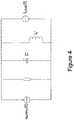
- the primary RLC circuit 500comprises a first inductor (L 1 ) 510, a first capacitor (C 1 ) 520 and a first resistor (R 1 ) 530.
- the secondary RLC circuit 600comprises a second inductor (L 2 ) 610, a second capacitor (C 2 ) 620 and a second resistor (R 2 ) 630.
- the primary RLC circuit 500is connected to a power source, comprising a time-dependent current source (i SUPPLY (t)) 540.
- the second RLC circuit 600is connected to a load, represented in Figure 2 as a DC current source (i LOAD ) 640.
- the current from the DC current source 640is zero when energy is not being transferred between the first and second RLC circuits 500, 600.
- the Q-values associated with the first and second resonator circuits 500, 600are represented by the first and second resistors 530, 630. As is explained in more detail below, the magnitude of the Q-values of the resonator circuits 500, 600 is proportional to the efficiency of energy transfer between the circuits 500, 600.
- the inductors 510, 610are separated by a distance approximately one order of magnitude greater than the physical dimensions of the inductors 510, 610 themselves.
- the coupling coefficient K between the inductors 510, 610is small, for example 0.001 or less, meaning that any attempt to transfer energy between the resonator circuits 500, 600 by conventional inductive coupling would be extremely inefficient.
- the coupling coefficient Khas a minimum value of zero and a maximum value of one.
- Figure 3shows an equivalent transformer circuit for the first and second RLC resonator circuits 500, 600.
- the frequency of the time-dependent current source 540is not equal to the resonant frequency f 0 of the second RLC resonator circuit 600, the second resonator circuit is bypassed due to negligible inductance LK. As such, very little or no power is transferred to the load. However, when the conditions for resonant inductive coupling are met, this situation is reversed as is explained in the example given below.
- the resonant frequencies f 0 of the resonator circuits 500, 600are equal to one another and the magnitudes of the Q-values (represented by the resistors 530, 630) of the resonator circuits 500, 600 are very high, for example one hundred or more or one thousand or more.
- current in the first inductor 510causes an evanescent magnetic field to be generated in the near field around the first inductor 510. This magnetic field is experienced by the second inductor 610 and causes a current to be induced.
- the impedances of the individual components of the equivalent transformer circuit shown in Figure 3are shown in Figure 5 .
- a secondary resonator circuitmay therefore be tuned so as to receive energy by resonant inductive coupling from any primary resonator circuit.
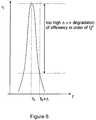
- Figure 6illustrates a general relationship between the efficiency of wireless energy transfer ⁇ through inductive coupling between primary and secondary reactances separated by a distance one order of magnitude larger than the physical dimensions of the reactances.
- the efficiency of wireless energy transfer ⁇is plotted on the vertical axis using a logarithmic scale, and the difference in resonant frequency f 0 between the reactances is plotted on the horizontal axis.
- This relationshipis applicable to, for example, non-radiative wireless energy transfer between the primary inductor 111 of the feeding device 100 and a secondary inductor 211 of a portable device 200 shown in Figure 7 .
- the efficiency of non-radiative wireless energy transfer ⁇ between the reactancesis at a maximum when the resonant frequencies f 0 associated with the reactances are equal to one another. Moreover, the efficiency of wireless energy transfer ⁇ between the reactances decreases markedly as the difference between the resonant frequencies f 0 associated with the reactances increases. Accordingly, as discussed above, in order to transfer energy at the maximum possible efficiency it is preferable for the reactances to have resonant frequencies f 0 which are as close to each other as possible. Ideally, the resonant frequencies f 0 should be identical.
- An optimal regime for efficient energy transfer by resonant inductive couplingmay be when the condition K 12 ⁇ 1 ⁇ 2 > > 1 is satisfied.
- ⁇represents the linewidth of the resonance associated with each of the first and second reactances due to intrinsic losses.
- the linewidthis inversely proportional to the Q factor, which is a measure of the sharpness of the resonance.
- the efficiency of energy transfer between primary and secondary reactancesis proportional to the magnitude of the Q-values associated with the reactances; for a high efficiency of energy transfer, the magnitude of the Q-values should be large.
- efficient energy transfermay be achieved with Q-values Q 111 , Q 211 in the order of 100 or more.
- the relative difference between the resonant frequencies f 0(111) , f 0(211) associated with the inductors 111, 211should be less that the reciprocal of their associated Q-values. At relative differences greater than the reciprocal of the Q-values, the efficiency of energy transfer decreases by 1/Q 2 .
- Figures 7 and 8illustrate the difference between conventional inductive coupling and resonant inductive coupling when the distance between reactances, for example the primary and secondary inductors 111, 211, is one order of magnitude greater than the reactances' physical dimensions.
- conventional inductive couplingi.e. when the difference between the resonant frequencies associated with the inductors 111, 211 is outside of the limits discussed above, only a negligible amount of energy in the magnetic field 400 is passed from the primary inductor 111 to the secondary inductor 211 in the portable device 200.
- the above examplediscusses the transfer of energy from a primary inductor 111 to a single secondary inductor 211.
- energycan be transferred from the primary inductor 111 to a plurality of secondary inductors 211 all being associated with the same resonant frequency f 0 , potentially enabling multiple portable devices 200 to receive energy wirelessly from a single feeding device 100.
- feeding devices 100are able to supply energy to portable electronic devices 200 over mid-ranges, for example several metres, in environments in which it is not convenient to install mains power sockets.
- a network 700 of feeding devices 100could be installed throughout a public space to provide members of the public with a power supply for their portable electronic devices 200.
- a public spacecould be, for example, a cafe, restaurant, bar, shopping mall or library.
- feeding devicesmay be installed in private spaces such as, for example, the interior of a person's car or home.
- the feeding devices 100have the capacity to supply energy to as many portable devices 200 as possible.
- One way in which this could be achievedis to implement a degree of standardization in the properties of the reactances, for example the primary and secondary inductors 111, 211, used in the feeding devices 100 and portable electronic devices 200.
- the resonant frequency f 0 associated with the primary reactance in each feeding device 100 of the network 700was the same. This would enable manufacturers of portable devices 200 and other electrical devices to equip their devices with secondary reactances associated with the same standardized resonant frequency f 0 .
- One way to alleviate this problemis to provide portable electronic devices 200 with a wireless energy transfer apparatus 210 for altering the resonant frequency f 0 associated with their secondary inductors 211 post-manufacture in dependence of the properties of a nearby feeding device 100.
- Thisprovides portable electronic devices 200 with the ability to tune their inductor's resonant frequency f 0 to match the frequency of an evanescent magnetic field generated around a primary inductor 111 in a nearby feeding device 100 and thus receive energy wirelessly by resonant inductive coupling.
- the portable electronic device 200comprises a wireless energy transfer apparatus 210, comprising a power supply unit (PSU), for receiving energy from a magnetic field and supplying electrical energy to electrical components 240 of the portable device 200.
- PSUpower supply unit
- electrical energymay be supplied to a rechargeable chemical battery 250 of the portable electronic device 200.
- the magnetic fieldwill be referred to in the context of the magnetic field 400 created by current flowing through the primary inductor 111 in a feeding device 100.
- the magnetic fieldcould alternatively correspond to a magnetic field created by another feeding device, or any other suitable magnetic field source.
- the wireless energy transfer apparatus 210may be controlled by a microcontroller 220 integrated into the energy transfer apparatus 210 and may comprise a receiving component 211a, comprising at least one reactance, for receiving energy wirelessly by non-radiative energy transfer from the magnetic field 400 by resonant inductive coupling. More specifically, as discussed above, a voltage may be induced in the receiving component 211a by the magnetic field 400 generated around the primary inductor 111 by an AC voltage applied across the primary inductor 111 at the supply source 110. When the receiving component 211a is coupled to a load in the portable electronic device, electrical power is transmitted from the supply source to the load. Such a load may comprise at least one switch mode power supply, as described with reference to Figure 10 .
- the receiving component 211acomprises a secondary inductor 211.
- the secondary inductor 211is associated with an inductance L 211 , Q-factor Q 211 and resonant frequency f 0(211) .
- the wireless energy transfer apparatus 210may further comprise monitoring circuitry 230 configured to detect a magnetic field 400 created around the primary inductor 111 in the feeding device 100, as is described in more detail below. Upon detecting the magnetic field 400, the monitoring circuitry 230 and microcontroller 220 may be further configured to detect and monitor the resonant frequency f 0(111) associated with the primary inductor 111.
- the features of the monitoring circuitry 230allow the portable device 200 to wirelessly receive energy over mid-range distances, for example distances at least one order of magnitude greater than the physical dimensions of the primary and secondary inductors 111, 211.
- the receiving component 211a of the wireless energy transfer apparatus 210has a parasitic capacitance C and is connected to a plurality of switched-mode power supplies (SMPSs) 212 via a diode-bridge 213 and LC filter 214.
- SMPSsswitched-mode power supplies
- the receiving componentis shown in Figure 10 as comprising a single secondary inductor 211, the receiving component 211a is adaptive and may be coupled to or comprise additional components for varying the resonant frequency. Examples of such components are shown in Figures 11 and 13 .
- the purpose of the LC filter 214is to ensure that a constant reactive load is introduced to the secondary inductor 211. If the inductor 211 were to be loaded resistively, there would be a significant decrease in the Q-value Q (211) associated with the inductor 211, which would in turn significantly reduce the efficiency of the transfer of energy from the feeding device 100, as previously discussed.
- the diode-bridge 213 and LC filter 214also protect the inductor 211 from direct exposure to the strongly time-varying load presented by the SMPSs 212, which are configured to supply power received by resonant inductive coupling from the magnetic field 400 to various circuits of the portable electronic device 200.
- the SMPSs 212may be configured, for example, to supply power to a rechargeable chemical battery 250 of the portable electronic device 200, as shown in Figure 9 , for recharging.
- the SMPSs 212may be configured to supply power directly to electrical components 240 of the portable electronic device 200, with the chemical battery 250 acting as a reserve power source.
- the chemical battery 250may be configured only to supply power to electrical components 240 of the portable electronic device 200 when the wireless energy transfer apparatus 210 is not receiving power by resonant inductive coupling. If feeding devices 100 were to become widespread, the inclusion of the rechargeable battery 250 in the portable device 200 could become unnecessary.
- FIG 11shows an example of an adaptive receiving component 211a.
- the resonance characteristics of the adaptive receiving component 211acan be tuned to match the resonance characteristics associated with the primary inductor 111 in the feeding device 100.
- An adaptive receiving component of this typeprovides the degree of tuneability necessary for the resonant frequency f 0(211) of the receiving component 211a to be varied, should the resonant frequency f 0(211) not be identical to that associated with the primary inductor 111 in the feeding device 100.
- the receiving component 211acomprises at least one secondary inductor 211 optionally coupled to an array of capacitors 215.
- Each capacitor 215may have a different capacitance to each of the others.
- the capacitors 215may comprise N capacitors with capacitances C 0 , C 0 /2,...C 0 /2 N-1 .
- Each of the capacitors 215may be optionally coupled to the secondary inductor 211 to affect the capacitance C 211 of the receiving component 211a, thereby varying the resonant frequency f 0(211) associated with the inductor 211.
- connection and disconnection of the capacitors 215 to the secondary inductor 211provides a mechanism by which the resonant frequency of the receiving component 211a can be varied to match the frequency of the transmitting primary inductor and thus receive energy by resonant inductive coupling.
- the portable device 200can therefore match the resonant frequency f 0(211) associated with the secondary inductor 211 with the resonant frequency f 0(111) associated with the primary inductor 111 in the feeding device 100. It will be appreciated that the resonant frequency f 0(111) associated with the secondary inductor 211 could alternatively be varied by altering the inductance of the receiving component 211a.
- the array of capacitors 215is coupled to a control unit 216 in the microcontroller 220 for automatically controlling the capacitance C 211 of the receiving component 211a in dependence of a control signal from the monitoring circuitry 230.
- the microcontroller 220may comprise a memory and signal processing means 217, for example including a microprocessor 218, configured to implement a computer program for detecting and monitoring the resonant frequency associated with the primary inductor 111 through the monitoring circuitry 230 and analysing the control signal from the monitoring circuitry 230 to cause the resonant frequency the resonant frequency associated with the secondary inductor 211 to be varied by connection and disconnection of the individual capacitors in the capacitor array 215.
- control unit 216is able to adapt the resonant frequency f 0(211) of the receiving component 211a to make it equal to the resonant frequency f 0(111) associated with the primary inductor 111, thereby initiating resonant inductive coupling between the primary inductor 111 and the secondary inductor 211.
- the monitoring circuitry 230may be coupled to an output from the LC filter 214 to detect when a voltage is being induced in the secondary inductor 211 and thus to detect when the portable electronic device 200 is in the presence of a magnetic field 400.
- the output of the LC filter 214may be coupled to an input of an AD converter 231, which may be integrated into the monitoring circuitry 230, for sensing a voltage induced in the secondary inductor 211 and for supplying a representative signal to the microcontroller 220 for calculating the resonant frequency associated with the primary inductor 111.
- the resonant frequency associated with the secondary inductor 211may then be varied by varying the resonant frequency of the adaptive receiving component 211a to match the calculated resonant frequency of the primary inductor 111.
- the monitoring circuitry 230may comprise a separate coil 232 for supplying induced voltage signals to the AD converter 231.
- the monitoring circuitry 230may be sensitive to very small voltages induced in the secondary inductor 211, for example of the order of microvolts, and may be configured such that it is able to detect a magnetic field 400 even when the receiving component 211a is in a detuned state.
- the monitoring circuitry 230is thus able to detect the presence of a primary inductor 111 even when then the resonant frequency f 0(111) associated with the primary inductor 111 is not equal to the resonant frequency f 0(211) set for the secondary inductor 211 in the portable electronic device 200.
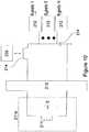
- the monitoring circuitry 230is comprised in an application specific integrated circuit (ASIC) 3000 for varying the resonant frequency f 0(211) of an adaptive receiving component 211a in dependence of the resonant frequency f 0(111) of a supply source 110 comprising a primary inductor 111.
- ASICapplication specific integrated circuit
- the receiving component 211amay comprise at least one secondary inductor 211
- the monitoring circuitrymay comprise a measurement coil 211b.
- the measurement coil 211bmay be external to the ASIC 3000.
- the measurement coil 211bmay have a high impedance value, such that current in the measurement coil 211b is negligible even when the measurement coil 211b is in the presence of a field 400 from a supply source 110.
- the inductance values L 211 and L 211b of the secondary inductor 211 and measurement coil 211bmay be measured at the time of manufacture of the portable device 200.
- the phase of the time varying voltage signal u 111 at the supply source 110may be calculated at the portable device 200 despite there being no physical connection between the portable device 200 and the supply source 110.
- the phase of the voltage signal u' 111may then be used to adjust the resonant frequency of the receiving component 211a as described in more detail below.
- the coupling coefficient K 211b-211 between the secondary inductor 211 and the measurement coil 211bmay be stored, for example, in non-volatile memory in the portable device 200 and may be recalled when the portable device 200 is in use.
- the voltage signals induced at the secondary inductor 211 and measurement coil 211b due to interaction with the magnetic field 400may be input to a phase comparator in the portable device 200, which is configured to compare the phase of the voltage u' 111 (equivalent to the phase of the voltage at the supply source 110) with the phase of the voltage u 211 at the secondary inductor 211.
- the phase difference between the voltage signalsmay be used to adjust the resonant frequency of the receiving component 211a in dependence of the resonant frequency associated with a primary inductor 111 in a supply source 110. This is described in more detail below.
- the portable device 200may comprise a phase comparator which is part of a phase locked loop (PLL) circuit 2000.
- the PLL circuit 2000may be part of the monitoring circuitry 230.
- the PLL circuit 2000may be implemented in the application specific integrated circuit 3000, and may be coupled to the control unit 216 for supplying a control signal to the control unit 216 to cause the resonant frequency f 0(211) of the receiving component 211a to be varied in dependence of the resonant frequency of the supply source 110.
- the PLL circuit 2000allows the resonant frequency of the receiving component 211a to be tuned to match the resonant frequency of the supply source 110 and to be varied in response to any variation in the resonant frequency of the supply source 110.
- the control unit 216is implemented in the ASIC 3000.
- the ASIC 3000comprises five functional blocks 3100, 3200, 3300, 3400, 3500.
- the first block 3100comprises first and second differential amplifiers 3110, 3120 configured to measure the voltages u 211 , u 211b induced at the secondary inductor 211 and the measurement coil 211b respectively by a magnetic field 400 generated around the primary inductor 111.
- the second block 3200comprises third and fourth differential amplifiers 3210, 3220, which are connected to receive the outputs from the first and second differential amplifiers 3110, 3120.
- the third and fourth differential amplifiers 3210, 3220are configured to output the time varying voltage u 211 at the secondary inductor 211 and the time varying voltage u' 111 respectively.
- the voltage u' 111is equivalent in phase to the voltage u 111 at the supply source 110.
- the signals from the third and fourth differential amplifiers 3210, 3220are fed to first and second analogue to digital converters (ADC) 3310, 3320, followed by first and second high pass filters 3330, 3340. This strips the DC component from the signal.
- ADCanalogue to digital converters
- the fourth block 3400comprises the phase comparator 3410, which in this example comprises an exclusive OR gate connected to receive at its inputs the most significant bit (MSB) from each of the high pass filters 3330, 3340.
- the phase difference between the voltage u 211 at the secondary inductor 211 and the voltage u 111 at the supply source 110may be ⁇ /2. Therefore, at resonance, the output of the exclusive OR gate 3410 may be high for half of each cycle (i.e. the duty cycle is 50%). This is a convenient equilibrium condition.
- the fifth block 3500comprises a low pass filter 3510, which is connected to receive the output from the phase comparator 3410 at its input and to output a control signal to the control unit 216 for controlling the value of the capacitance of the receiving component 211a, thereby varying the resonant frequency f 0(211) of the receiving component 211a in dependence of the resonant frequency of the supply source 110.
- Figure 12shows the adaptive receiving component as comprising a single inductor and capacitor.
- the structure of the adaptive receiving component 211amay include or correspond to the receiving components shown in Figures 11 and 13 .
- the receiving componentmay comprise or be coupled to additional components for varying the resonant frequency. Examples of such components are shown in Figures 11 and 13 .
- the couplings between the receiving components 211a and the switched mode power supplies 212have been omitted.
- the receiving components 211a shown in Figures 11 to 13may be coupled to one or more switched mode power supplies 212 for supplying power to electrical components of the portable electronic device, for example as shown in Figure 10 .
- the input impedance of the second block 3200is adjusted such that the output of the differential amplifiers 3210, 3220 in the second block 3200 is negligible in the absence of a field 400 from a supply source 110.
- Thismay be achieved, for example, by integrating a variable impedance component 3230 as shown in Figure 12 and setting the value of the variable impedance component 3230 to ensure that the output of the differential amplifier 3210 is negligible in the absence of a field 400.
- the value of the variable impedance component 3230may be set during manufacture or testing of the portable device 200, for example using conductive mode stimulus.
- the optimal input impedance value for the variable impedance component 3230may be stored in non volatile memory for later use.
- phase differenceThe component of the phase difference arising due to this factor (described below as an "apparent” component in the phase difference) varies due to manufacturing tolerances etc. in the components of the relevant circuits. Eliminating this "apparent" component of the phase difference prevents synchronisation of the PLL from being impaired and thus also prevents the PLL circuit from being driven towards a false equilibrium.
- the receiving component 211amay comprise a pair of secondary inductors 211 coupled to a fixed value capacitor 4000 and first and second varactor diodes 5000, 6000.
- the pair of secondary inductors 211may be replaced by a single inductor 211 having two symmetrical portions and a centre tap between the portions.
- the first and second varactor diodes 5000, 6000are coupled to receive a control signal from the PLL circuit 2000 (e.g. via the control unit 216) and are configured such that the capacitance of the varactor diodes 5000, 6000 varies in response to the output of the PLL circuit 2000.
- varactor diodes 5000, 6000provides a means of introducing a continuous range of potential capacitance values for the receiving component 211a, and thus a means of varying the resonant frequency of the receiving component 211a in dependence of the resonant frequency of the supply source 110. Furthermore, the use of varactor diodes 5000, 600 provides an inexpensive and compact means for varying the capacitance of the receiving component 211a. As shown in Figure 13 , this implementation of the receiving component 211a is symmetrical with respect to ground, or a reference potential.
- the wireless energy transfer apparatus 210may include a memory 219 for storing frequency values corresponding to resonant frequencies fo in different environments, such that the resonant frequency associated with the secondary inductor 211 can be automatically adjusted upon the portable electronic device 200 entering a particular environment. For example, such automatic adjustment could be prompted by a control signal, received through an aerial of the portable device 200, indicating that the device 200 has entered a familiar environment.
- the memory 219may also be suitable for storing tuning values between various life cycle states.
- the memory 219may comprise non-volatile memory in order that the various resonant frequency values fo stored in the memory 219 are not lost when the device 200 is switched-off.
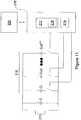
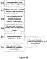
- Steps associated with the initiation of a wireless energy transfer between a supply source 110, for example comprising a primary inductor 111, and the portable electronic device 200 in the manner described aboveare shown in Figure 12 .
- the first step S1is to detect the presence of the supply source 110 by detecting the presence of its associated magnetic field 400 from an induced voltage at the monitoring circuitry 230.
- the supply source 110may comprise a primary inductor 111 in a feeding device 100.
- the second step S2is to calculate and monitor the resonant frequency of the supply source 110, and the third step S3 is vary the resonant frequency of the receiving component 211a, comprising the secondary inductor 211, in dependence of the resonant frequency of the supply source 110.
- the third step S3involves matching the resonant frequency of the receiving component 211a with the resonant frequency of the supply source 110.
- the fourth step S4is to receive energy wirelessly from the supply source 110 at the receiving component 211a by resonant inductive coupling
- the fifth step S5is to supply the energy to one or more components 240 of the portable device 200.
- the chemical battery 250may be configured to supply electrical energy to the components 240 of the portable device 200 in step S6. As shown by Figure 12 , in step S7, the supply of electrical energy from the battery 250 is ceased when wireless energy transfer by resonant inductive coupling is reinitiated.
- an adaptive receiving component 211ato vary the resonant frequency associated with the secondary inductor 211 in a portable electronic device 200 so as to match the resonant frequency associated with the secondary inductor 211 to a detected resonant frequency associated with a primary inductor 111 in a feeding device 100.
- an adaptive componentcould alternatively be employed in a feeding device 100 so as match the resonant frequency associated with a primary inductor in the feeding device 100 to that of a secondary inductor in a portable electronic device.
- a portable electronic device 200may be configured to supply a control signal to a feeding device 100 in order to supply the feeding device 100 with the resonance characteristics of the secondary inductor in the portable electronic device.
- the feeding device 100would then be able to match the resonant frequency associated with its primary inductor to the resonant frequency associated with the secondary inductor in the portable device 200, thereby initiating wireless energy transfer by resonant inductive coupling.
- the supply source of a feeding devicemay comprise a primary inductor driven by an amplifier, and the microcontroller of the portable electronic device may be configured to match a resonant frequency of the adaptive receiving component to a detected frequency of a magnetic field associated with the supply source.
- the portable device 200comprises a mobile telephone or PDA.
- the portable devicemay alternatively comprise any number of other devices, for example a laptop computer or digital music player.
- the inventionis not limited to the supply of power to portable electronic devices, but may be used for powering a wide variety of other electrical devices.
- a network of feeding devicesmay be installed in the home for supplying power to electric lamps and other household appliances.
Landscapes
- Engineering & Computer Science (AREA)
- Computer Networks & Wireless Communication (AREA)
- Power Engineering (AREA)
- Charge And Discharge Circuits For Batteries Or The Like (AREA)
- Near-Field Transmission Systems (AREA)
- Burglar Alarm Systems (AREA)
- Measurement Of Resistance Or Impedance (AREA)
- Magnetic Resonance Imaging Apparatus (AREA)
Description
- The present invention relates to wireless energy transfer, particularly, but not exclusively, to wireless energy transfer between a supply source and a receiving component.
- It is common practice for a portable electronic device, for example a mobile telephone or a laptop computer, to be powered by a rechargeable chemical battery. Generally speaking, such a battery is releasably connected to the body of a portable device.
- The use of a battery for supplying power to a portable electronic device is not ideal because the energy storage capacity of a chemical battery is limited. As such, it is necessary for the chemical battery to be recharged at regular intervals.
- In order to provide a means for recharging the battery, the portable device is normally supplied with a charger unit to allow electrical energy to flow from a mains power supply to the rechargeable battery. The charger unit conventionally comprises an electrical plug for connecting to a mains power supply socket and an electrical cable for connecting the electrical plug to the portable device.
- This is disadvantageous because, if there is no convenient mains power supply socket, as is the case in most outdoor and public environments, the rechargeable battery will run out of power and the portable device will need to be switched off.
- The use of such a charger unit is further disadvantageous in that it requires a physical connection between the portable device and a mains power supply socket. This severely restricts the movement of the portable device during charging, thereby negating the portability of the device.
- Another type of charger unit makes use of the principle of conventional, short-range inductive coupling, which involves the transfer of energy from a primary inductor in a charger unit to a secondary inductor in the portable device. Such charger units are commonly used, for example, for charging rechargeable batteries in electric toothbrushes.
- Chargers utilising this type of conventional inductive coupling are able to transfer power wirelessly and hence do not require a physical connection between the mains supply and the portable device. However, the maximum distance over which effective power transfer can be achieved is limited to distances of the same order of magnitude as the physical dimensions of the inductors. For portable electronic devices, the dimensions of the inductor are limited by the size of the portable electronic device. Accordingly, in general, at distances of anything greater than a few centimetres, the efficiency of energy transfer between primary and secondary inductors is too small for this type of power transfer to be viable.
- Therefore, as with the electrical cable discussed above, power transfer using conventional inductive coupling requires the charger unit and the portable device to be in very close proximity, meaning that the movement of the portable device is severely restricted.
- In addition to the above problems associated with recharging, the use of a chemical battery as a power supply presents a number of further disadvantages. For example, rechargeable chemical batteries have a limited lifespan and tend to experience a decrease in their maximum storage capacity as they get older. Furthermore, chemical batteries are relatively heavy, meaning that the inclusion of a chemical battery in a portable device generally adds a significant percentage to the device's overall weight. If the device's reliance on the chemical battery could be reduced, then it would be possible for portable electronic devices such as mobile telephones to become significantly lighter.
US 7208912 discloses inductive battery charging with peak voltage detection.US 2007/0145830 discloses a system and method for inductive transfer of electrical power between a substantially flat primary surface and a multitude of secondary devices in such a way that power transfer is localized to the vicinities of the individual device coils.- The invention is set forth in the claims.
- This specification describes an apparatus comprising monitoring circuitry configured to monitor a resonant frequency of a supply source, a receiving component, and a control unit configured to vary a resonant frequency of said receiving component, wherein the apparatus is configured to vary the resonant frequency of said receiving component in dependence upon the resonant frequency of said supply source
- The receiving component is adapted to receive energy wirelessly from the supply source by resonant inductive coupling.
- The receiving component may comprise an adaptive receiving component having a variable resonant frequency.
- The apparatus is configured to match the resonant frequency of said receiving component with the resonant frequency of said supply source.
- A voltage is induced in the receiving component by a magnetic field generated by the supply source, and the control unit is configured to vary the resonant frequency of the receiving component to match the resonant frequency of the supply source.
- The apparatus may further comprise a plurality of electrical components, and the apparatus may be configured to supply electrical energy to at least one of these electrical components.
- The apparatus may further comprise a battery for supplying electrical energy to at least one of the electrical components when energy is not being received from the supply source.
- The apparatus may comprise a portable electronic device. The apparatus may comprise a mobile telephone, personal digital assistant (PDA) or laptop computer.
- The apparatus comprises a phase locked loop circuit configured to output a control signal for varying the resonant frequency of the receiving component in dependence upon the resonant frequency of the supply source.
- This specification further describes an apparatus comprising means for detecting a presence of a supply source, means for monitoring a resonant frequency of said supply source, and means for varying a resonant frequency of a receiving component in dependence upon the resonant frequency of said supply source.
- The receiving component may be configured to receive electrical energy by wireless non-radiative energy transfer from the supply source and may be configured to supply the received electrical energy to a rechargeable battery.
- This specification further describes an apparatus comprising a receiving component having variable resonance characteristics for receiving energy wirelessly from a supply source, wherein the resonance characteristics of the receiving component may be varied to match resonance characteristics of the supply source to increase the efficiency at which energy is received from the supply source.
- The apparatus may further comprise monitoring circuitry for detecting and monitoring the resonance characteristics of the supply source.
- The receiving component of the apparatus may comprise an adaptive receiving component having variable resonance characteristics and the apparatus may further comprise a control unit configured to automatically vary the resonance characteristics of the adaptive receiving component to match the resonance characteristics of the supply source.
- The apparatus may further comprise one or more electrical components and the receiving component may be coupled to power supply circuitry to supply power to at least one of these electrical components.
- The apparatus may further comprise a battery for supplying electrical energy to at least one of the electrical components when energy is not being received from the supply source.
- The apparatus may comprise a portable electronic device.
- The apparatus may comprise a mobile telephone, personal digital assistant (PDA) or laptop computer.
- The apparatus comprise a phase locked loop circuit configured to output a control signal for varying the resonant frequency of the receiving component in dependence of the resonant frequency of the supply source.
- This specification further describes a system comprising a supply source, and an apparatus comprising monitoring circuitry configured to monitor a resonant frequency of the supply source, a receiving component, and a control unit configured to vary a resonant frequency of said receiving component, wherein the apparatus is configured to vary the resonant frequency of said receiving component in dependence upon the resonant frequency of said supply source.
- This specification further describes a method comprising detecting a presence of a supply source, monitoring a resonant frequency of said supply source, and varying a resonant frequency of a receiving component in dependence upon the resonant frequency of said supply source.
- The method may further comprise outputting a control signal from a phase locked loop circuit for varying the resonant frequency of the receiving component in dependence upon the resonant frequency of the supply source, and matching the resonant frequency of said receiving component with the resonant frequency of said supply source.
- The method may further comprise receiving energy wirelessly at the receiving component from the supply source by resonant inductive coupling.
- The receiving component may comprise an adaptive receiving component having a variable resonant frequency and the method may further comprise inducing a voltage in the adaptive receiving component using a magnetic field generated by the supply source, and varying the resonant frequency of the adaptive receiving component to match the resonant frequency of the supply source.
- The method may further comprise supplying electrical energy to an electrical apparatus.
- The method may further comprise supplying energy to at least one component of an electrical device from a battery when energy is not being received at the receiving component from the supply source.
- The method may further comprise receiving energy at the receiving component from the supply source by resonant inductive coupling, and supplying energy received by resonant inductive coupling to at least one component of an electrical device.
- This specification further describes a computer program stored on a storage-medium which, when executed by a processor, is arranged to perform a method comprising detecting a presence of a supply source, monitoring a resonant frequency of said supply source, and varying a resonant frequency of a receiving component in dependence of the resonant frequency of said supply source.
- In order that the invention may be more fully understood, embodiments thereof will now be described by way of illustrative example with reference to the accompanying drawings in which:
Figure 1 is a diagram showing a flow of energy from a feeding device to a portable electronic device.Figure 2 is a circuit diagram of primary and secondary RLC resonator circuits with coupling coefficient K.Figure 3 is a circuit diagram of an equivalent transformer circuit for the first and second RLC resonator circuits shown inFigure 2 .Figure 4 is a circuit diagram of a reduced circuit of the equivalent transformer circuit shown inFigure 3 .Figure 5 shows the impedances of the individual components of the equivalent transformer circuit shown inFigure 3 .Figure 6 is a graphical illustration of the relationship between the efficiency of power transfer between two resonators and the difference between the resonators' resonant frequencies.Figure 7 is an illustration of a wireless transfer of energy from a feeding device to a portable electronic device at mid-range using conventional inductive coupling.Figure 8 is an illustration of a wireless transfer of energy from a feeding device to a portable electronic device at mid-range using resonant inductive coupling.Figure 9 is a schematic diagram of a portable electronic device, including a reactance and monitoring circuitry.Figure 10 is a schematic diagram showing components of a wireless power transfer apparatus in a portable electronic device.Figure 11 is a schematic diagram showing an adaptive receiving component in a wireless power transfer apparatus of a portable electronic device.Figure 12 is a circuit diagram showing an example set of components in a PLL ASIC comprised in a wireless power transfer apparatus of a portable device.Figure 13 is a circuit diagram showing an example of an adaptive receiving component and a measurement coil for feeding signals to the PLL ASIC.Figure 14 is a flow diagram showing steps associated with the initiation of wireless power transfer by resonant inductive coupling.- The invention is set out in the appended set of claims. The embodiments and/or examples of the following description which are not covered by the appended claims are considered as not being part of the present invention. Referring to
Figure 1 , afeeding device 100 comprises asupply source 110 for supplying power wirelessly to a portableelectronic device 200. Thesupply source 110 comprises a primary reactance, for example comprising aprimary inductor 111, coupled to anelectrical circuit 112. Theelectrical circuit 112 may be optionally connected to a power supply, for example comprising amains power supply 300, for supplying electrical current to theelectrical circuit 112. Theprimary inductor 111 has an inductance L111, Q-factor Q111 and resonant frequency f0(111). - As will be understood by a skilled person, a flow of electrical current through the
primary inductor 111 causes amagnetic field 400 to be created around theprimary inductor 111. As is shown byFigure 1 , the evanescentmagnetic field 400 created around theinductor 111 penetrates the exterior of thefeeding device 100, meaning that the effects of themagnetic field 400 may be experienced in the surrounding environment. For instance, themagnetic field 400 may be used to induce a voltage in a receiving component comprising a secondary reactance, such as a secondary inductor in an electrical device. This is the principle upon which wireless non-radiative energy transfer through conventional short-range inductive coupling is based. However, efficient wireless energy transfer by such conventional short-range inductive coupling is limited to distances of the same order of magnitude as the physical dimensions of the inductors involved in the energy transfer. - As is fully described below, the portable
electronic device 200 is adapted to receive energy wirelessly by an alternative type of inductive coupling. This alternative type of inductive coupling will be referred to as resonant inductive coupling. - Using resonant inductive coupling, it is possible to use non-radiative energy transfer to transfer energy efficiently over longer distances than over those possible with conventional inductive coupling. This means that resonant inductive coupling provides a greater degree of freedom and flexibility than conventional inductive coupling when used for the transfer of energy. As is described in more detail below, resonant inductive coupling is based on inductive coupling between a supply source and a receiving component that contain inductors critically tuned to the same frequency. The inductor at the receiving component may tuned so as to resonate at the frequency of the supply source inductor. For example, the resonant frequency f0 of a supply source and the resonant frequency f0 of a receiving component may be equal to one another.
- More specifically, if the resonant frequency f0 associated with a primary reactance, for example the resonant frequency f0(111) associated with the
inductor 111 in thefeeding device 100, may be equal to the resonant frequency f0 associated with a secondary reactance, for example a receiving component comprising a secondary inductor in a portableelectronic device 200, efficient wireless non-radiative energy transfer can be achieved between the primary and secondary reactances at longer ranges than is possible with conventional inductive coupling if the primary reactance is placed in a magnetic field generated around the primary reactance. - For example, wireless energy transfer with an efficiency of tens of percent may be achieved by resonant inductive coupling over distances at least one order of magnitude greater than the physical dimensions of the inductors being used for the transfer.
- A general example of non-radiative wireless energy transfer between two inductors by resonant inductive coupling is given below.
- Referring to
Figure 2 , there are shown primary and secondaryRLC resonator circuits primary RLC circuit 500 comprises a first inductor (L1) 510, a first capacitor (C1) 520 and a first resistor (R1) 530. Thesecondary RLC circuit 600 comprises a second inductor (L2) 610, a second capacitor (C2) 620 and a second resistor (R2) 630. In this example, L1= L2 and C1= C2. - The
primary RLC circuit 500 is connected to a power source, comprising a time-dependent current source (iSUPPLY(t)) 540. The time-dependency of thecurrent source 540 is such that the current may take the form of a sine wave, tuned to the resonant frequency f0 of both the first andsecond RLC circuits 
- The
second RLC circuit 600 is connected to a load, represented inFigure 2 as a DC current source (iLOAD) 640. The current from the DCcurrent source 640 is zero when energy is not being transferred between the first andsecond RLC circuits - The Q-values associated with the first and
second resonator circuits second resistors 530, 630. As is explained in more detail below, the magnitude of the Q-values of theresonator circuits circuits - In this general example, the
inductors inductors inductors resonator circuits 
resonator circuits Figure 3 shows an equivalent transformer circuit for the first and secondRLC resonator circuits current source 540 is not equal to the resonant frequency f0 of the secondRLC resonator circuit 600, the second resonator circuit is bypassed due to negligible inductance LK. As such, very little or no power is transferred to the load. However, when the conditions for resonant inductive coupling are met, this situation is reversed as is explained in the example given below.- In one example of energy transfer by resonant inductive coupling, the resonant frequencies f0 of the
resonator circuits resonator circuits current source 540 at the resonant frequency f0 of:
first inductor 510 causes an evanescent magnetic field to be generated in the near field around thefirst inductor 510. This magnetic field is experienced by thesecond inductor 610 and causes a current to be induced. In this way, current in thefirst inductor 510 is routed via thesecond inductor 610. Under these conditions, the inductance LK in the equivalent transformer circuit shown inFigure 3 is tuned with the secondary resonator circuit. As such, the equivalent transformer circuit shown inFigure 3 can be reduced to the circuit of a single electrical resonator, as shown byFigure 4 . There is no limit on the number of secondary resonator circuits which could receive current from a primary resonator circuit in this way. - The impedances of the individual components of the equivalent transformer circuit shown in
Figure 3 are shown inFigure 5 . The impedance Z of the reduced circuit can thus be calculated as follows:
- If the Q-value of the
secondary resonator circuit 600 is high, Zsecondary may be written as:

- A secondary resonator circuit may therefore be tuned so as to receive energy by resonant inductive coupling from any primary resonator circuit.
Figure 6 illustrates a general relationship between the efficiency of wireless energy transfer η through inductive coupling between primary and secondary reactances separated by a distance one order of magnitude larger than the physical dimensions of the reactances. The efficiency of wireless energy transfer η is plotted on the vertical axis using a logarithmic scale, and the difference in resonant frequency f0 between the reactances is plotted on the horizontal axis. This relationship is applicable to, for example, non-radiative wireless energy transfer between theprimary inductor 111 of thefeeding device 100 and asecondary inductor 211 of aportable device 200 shown inFigure 7 .- As can be seen, the efficiency of non-radiative wireless energy transfer η between the reactances is at a maximum when the resonant frequencies f0 associated with the reactances are equal to one another. Moreover, the efficiency of wireless energy transfer η between the reactances decreases markedly as the difference between the resonant frequencies f0 associated with the reactances increases. Accordingly, as discussed above, in order to transfer energy at the maximum possible efficiency it is preferable for the reactances to have resonant frequencies f0 which are as close to each other as possible. Ideally, the resonant frequencies f0 should be identical.
- An optimal regime for efficient energy transfer by resonant inductive coupling may be when the condition

- In addition, as previously discussed, the efficiency of energy transfer between primary and secondary reactances is proportional to the magnitude of the Q-values associated with the reactances; for a high efficiency of energy transfer, the magnitude of the Q-values should be large. For example, in the case of the primary and
secondary inductors feeding device 100 to theportable device 200, efficient energy transfer may be achieved with Q-values Q111, Q211 in the order of 100 or more. Furthermore, the relative difference between the resonant frequencies f0(111), f0(211) associated with theinductors Figures 7 and8 illustrate the difference between conventional inductive coupling and resonant inductive coupling when the distance between reactances, for example the primary andsecondary inductors Figure 7 , with conventional inductive coupling, i.e. when the difference between the resonant frequencies associated with theinductors magnetic field 400 is passed from theprimary inductor 111 to thesecondary inductor 211 in theportable device 200. In contrast, referring toFigure 8 , when the resonant frequencies f0 associated with theinductors primary inductor 111 in thefeeding device 100 to thesecondary inductor 211 in the portableelectronic device 200 via themagnetic field 400.- For the purposes of simplicity and clarity, the above example discusses the transfer of energy from a
primary inductor 111 to a singlesecondary inductor 211. However, alternatively, energy can be transferred from theprimary inductor 111 to a plurality ofsecondary inductors 211 all being associated with the same resonant frequency f0, potentially enabling multipleportable devices 200 to receive energy wirelessly from asingle feeding device 100. - In this way, feeding
devices 100 are able to supply energy to portableelectronic devices 200 over mid-ranges, for example several metres, in environments in which it is not convenient to install mains power sockets. As an example, in a similar manner to the installation of wireless LANS in cafés and restaurants, anetwork 700 of feedingdevices 100 could be installed throughout a public space to provide members of the public with a power supply for their portableelectronic devices 200. Such a public space could be, for example, a cafe, restaurant, bar, shopping mall or library. Alternatively, feeding devices may be installed in private spaces such as, for example, the interior of a person's car or home. - In order to maximise the potential of such a
network 700 of feedingdevices 100, it is preferable that thefeeding devices 100 have the capacity to supply energy to as manyportable devices 200 as possible. One way in which this could be achieved is to implement a degree of standardization in the properties of the reactances, for example the primary andsecondary inductors feeding devices 100 and portableelectronic devices 200. In particular, it would be preferable if the resonant frequency f0 associated with the primary reactance in eachfeeding device 100 of thenetwork 700 was the same. This would enable manufacturers ofportable devices 200 and other electrical devices to equip their devices with secondary reactances associated with the same standardized resonant frequency f0. - A skilled person will appreciate, however, that due to manufacturing tolerances, the mass production of inductors to a degree of accuracy in which all the inductors are associated with exactly the same resonant frequency f0 may be difficult to achieve. This will lead to variations in both the resonant frequencies f0 of feeding
devices 100, and to variations in the resonant frequencies f0 ofportable devices 200. Furthermore, even if feedingdevices 100 andportable devices 200 can be manufactured with identical resonant frequencies f0 in free space, the resonant frequencies f0 of each individual unit will be affected when in use by other inductors in the unit's surrounding environment. The amount by which the resonant frequency of each unit is altered will depend on the number and proximity of other inductors. - Thus, even when attempts have been made to standardize the resonant frequencies f0 of feeding devices and portable devices, manufacturing intolerances and environmental conditions still have the potential to cause problems for energy transfer by resonant inductive coupling.
- One way to alleviate this problem is to provide portable
electronic devices 200 with a wirelessenergy transfer apparatus 210 for altering the resonant frequency f0 associated with theirsecondary inductors 211 post-manufacture in dependence of the properties of anearby feeding device 100. This provides portableelectronic devices 200 with the ability to tune their inductor's resonant frequency f0 to match the frequency of an evanescent magnetic field generated around aprimary inductor 111 in anearby feeding device 100 and thus receive energy wirelessly by resonant inductive coupling. - An exemplary embodiment of a portable
electronic device 200 adapted to receive energy wirelessly by resonant inductive coupling is given below. Referring toFigure 9 , the portableelectronic device 200 comprises a wirelessenergy transfer apparatus 210, comprising a power supply unit (PSU), for receiving energy from a magnetic field and supplying electrical energy toelectrical components 240 of theportable device 200. Alternatively, as discussed below, electrical energy may be supplied to arechargeable chemical battery 250 of the portableelectronic device 200. - In the example discussed below, the magnetic field will be referred to in the context of the
magnetic field 400 created by current flowing through theprimary inductor 111 in afeeding device 100. However, a skilled person will appreciate that the magnetic field could alternatively correspond to a magnetic field created by another feeding device, or any other suitable magnetic field source. - The wireless
energy transfer apparatus 210 may be controlled by amicrocontroller 220 integrated into theenergy transfer apparatus 210 and may comprise areceiving component 211a, comprising at least one reactance, for receiving energy wirelessly by non-radiative energy transfer from themagnetic field 400 by resonant inductive coupling. More specifically, as discussed above, a voltage may be induced in thereceiving component 211a by themagnetic field 400 generated around theprimary inductor 111 by an AC voltage applied across theprimary inductor 111 at thesupply source 110. When thereceiving component 211a is coupled to a load in the portable electronic device, electrical power is transmitted from the supply source to the load. Such a load may comprise at least one switch mode power supply, as described with reference toFigure 10 . In this example, the receivingcomponent 211a comprises asecondary inductor 211. Thesecondary inductor 211 is associated with an inductance L211, Q-factor Q211 and resonant frequency f0(211). - The wireless
energy transfer apparatus 210 may further comprisemonitoring circuitry 230 configured to detect amagnetic field 400 created around theprimary inductor 111 in thefeeding device 100, as is described in more detail below. Upon detecting themagnetic field 400, themonitoring circuitry 230 andmicrocontroller 220 may be further configured to detect and monitor the resonant frequency f0(111) associated with theprimary inductor 111. - The features of the
monitoring circuitry 230 allow theportable device 200 to wirelessly receive energy over mid-range distances, for example distances at least one order of magnitude greater than the physical dimensions of the primary andsecondary inductors - Referring to
Figure 10 in combination withFigure 9 , in one example thereceiving component 211a of the wirelessenergy transfer apparatus 210 has a parasitic capacitance C and is connected to a plurality of switched-mode power supplies (SMPSs) 212 via a diode-bridge 213 andLC filter 214. Although the receiving component is shown inFigure 10 as comprising a singlesecondary inductor 211, the receivingcomponent 211a is adaptive and may be coupled to or comprise additional components for varying the resonant frequency. Examples of such components are shown inFigures 11 and13 . The purpose of theLC filter 214 is to ensure that a constant reactive load is introduced to thesecondary inductor 211. If theinductor 211 were to be loaded resistively, there would be a significant decrease in the Q-value Q(211) associated with theinductor 211, which would in turn significantly reduce the efficiency of the transfer of energy from thefeeding device 100, as previously discussed. - The diode-
bridge 213 andLC filter 214 also protect theinductor 211 from direct exposure to the strongly time-varying load presented by theSMPSs 212, which are configured to supply power received by resonant inductive coupling from themagnetic field 400 to various circuits of the portableelectronic device 200. TheSMPSs 212 may be configured, for example, to supply power to arechargeable chemical battery 250 of the portableelectronic device 200, as shown inFigure 9 , for recharging. - Alternatively the
SMPSs 212 may be configured to supply power directly toelectrical components 240 of the portableelectronic device 200, with thechemical battery 250 acting as a reserve power source. For example, thechemical battery 250 may be configured only to supply power toelectrical components 240 of the portableelectronic device 200 when the wirelessenergy transfer apparatus 210 is not receiving power by resonant inductive coupling. If feedingdevices 100 were to become widespread, the inclusion of therechargeable battery 250 in theportable device 200 could become unnecessary. Figure 11 shows an example of anadaptive receiving component 211a. The resonance characteristics of theadaptive receiving component 211a can be tuned to match the resonance characteristics associated with theprimary inductor 111 in thefeeding device 100. An adaptive receiving component of this type provides the degree of tuneability necessary for the resonant frequency f0(211) of thereceiving component 211a to be varied, should the resonant frequency f0(211) not be identical to that associated with theprimary inductor 111 in thefeeding device 100.- In one example, as is shown by
Figure 11 , the receivingcomponent 211a comprises at least onesecondary inductor 211 optionally coupled to an array ofcapacitors 215. Eachcapacitor 215 may have a different capacitance to each of the others. For example, as shown byFigure 11 , thecapacitors 215 may comprise N capacitors with capacitances C0, C0/2,...C0/2N-1. Each of thecapacitors 215 may be optionally coupled to thesecondary inductor 211 to affect the capacitance C211 of thereceiving component 211a, thereby varying the resonant frequency f0(211) associated with theinductor 211. The connection and disconnection of thecapacitors 215 to thesecondary inductor 211 provides a mechanism by which the resonant frequency of thereceiving component 211a can be varied to match the frequency of the transmitting primary inductor and thus receive energy by resonant inductive coupling. Theportable device 200 can therefore match the resonant frequency f0(211) associated with thesecondary inductor 211 with the resonant frequency f0(111) associated with theprimary inductor 111 in thefeeding device 100. It will be appreciated that the resonant frequency f0(111) associated with thesecondary inductor 211 could alternatively be varied by altering the inductance of thereceiving component 211a. - In this implementation, as is shown by
Figure 11 , the array ofcapacitors 215 is coupled to acontrol unit 216 in themicrocontroller 220 for automatically controlling the capacitance C211 of thereceiving component 211a in dependence of a control signal from themonitoring circuitry 230. Themicrocontroller 220 may comprise a memory and signal processing means 217, for example including amicroprocessor 218, configured to implement a computer program for detecting and monitoring the resonant frequency associated with theprimary inductor 111 through themonitoring circuitry 230 and analysing the control signal from themonitoring circuitry 230 to cause the resonant frequency the resonant frequency associated with thesecondary inductor 211 to be varied by connection and disconnection of the individual capacitors in thecapacitor array 215. - In this way, the
control unit 216 is able to adapt the resonant frequency f0(211) of thereceiving component 211a to make it equal to the resonant frequency f0(111) associated with theprimary inductor 111, thereby initiating resonant inductive coupling between theprimary inductor 111 and thesecondary inductor 211. - The
monitoring circuitry 230 may be coupled to an output from theLC filter 214 to detect when a voltage is being induced in thesecondary inductor 211 and thus to detect when the portableelectronic device 200 is in the presence of amagnetic field 400. For example, the output of theLC filter 214 may be coupled to an input of anAD converter 231, which may be integrated into themonitoring circuitry 230, for sensing a voltage induced in thesecondary inductor 211 and for supplying a representative signal to themicrocontroller 220 for calculating the resonant frequency associated with theprimary inductor 111. The resonant frequency associated with thesecondary inductor 211 may then be varied by varying the resonant frequency of theadaptive receiving component 211a to match the calculated resonant frequency of theprimary inductor 111. - Alternatively, as shown by
Figure 9 , themonitoring circuitry 230 may comprise aseparate coil 232 for supplying induced voltage signals to theAD converter 231. - The
monitoring circuitry 230 may be sensitive to very small voltages induced in thesecondary inductor 211, for example of the order of microvolts, and may be configured such that it is able to detect amagnetic field 400 even when thereceiving component 211a is in a detuned state. Themonitoring circuitry 230 is thus able to detect the presence of aprimary inductor 111 even when then the resonant frequency f0(111) associated with theprimary inductor 111 is not equal to the resonant frequency f0(211) set for thesecondary inductor 211 in the portableelectronic device 200. - Referring to
Figures 12 and13 , in one example, themonitoring circuitry 230 is comprised in an application specific integrated circuit (ASIC) 3000 for varying the resonant frequency f0(211) of anadaptive receiving component 211a in dependence of the resonant frequency f0(111) of asupply source 110 comprising aprimary inductor 111. In this example, the receivingcomponent 211a may comprise at least onesecondary inductor 211, and the monitoring circuitry may comprise ameasurement coil 211b. Themeasurement coil 211b may be external to theASIC 3000. Themeasurement coil 211b may have a high impedance value, such that current in themeasurement coil 211b is negligible even when themeasurement coil 211b is in the presence of afield 400 from asupply source 110. The time varying voltage u211b induced in themeasurement coil 211b by a magnetic field generated around aprimary inductor 111 in asupply source 110 may be written as follows:
- Rearrangement of this equation allows the time varying voltage u211b measured in the
measurement coil 211b to be used to calculate the unknown phase of the time varying voltage u111 at theprimary inductor 111 in thesupply source 110, as follows:
supply source 110. - The inductance values L211 and L211b of the
secondary inductor 211 andmeasurement coil 211b may be measured at the time of manufacture of theportable device 200. As such, by measuring the coupling coefficient K211b-211 between thesecondary inductor 211 and themeasurement coil 211b (e.g. during manufacture of the portable device 200), the phase of the time varying voltage signal u111 at thesupply source 110 may be calculated at theportable device 200 despite there being no physical connection between theportable device 200 and thesupply source 110. The phase of the voltage signal u'111 may then be used to adjust the resonant frequency of thereceiving component 211a as described in more detail below. Once measured, the coupling coefficient K211b-211 between thesecondary inductor 211 and themeasurement coil 211b may be stored, for example, in non-volatile memory in theportable device 200 and may be recalled when theportable device 200 is in use. - The voltage signals induced at the
secondary inductor 211 andmeasurement coil 211b due to interaction with themagnetic field 400 may be input to a phase comparator in theportable device 200, which is configured to compare the phase of the voltage u'111 (equivalent to the phase of the voltage at the supply source 110) with the phase of the voltage u211 at thesecondary inductor 211. The phase difference between the voltage signals may be used to adjust the resonant frequency of thereceiving component 211a in dependence of the resonant frequency associated with aprimary inductor 111 in asupply source 110. This is described in more detail below. - Referring to
Figures 12 and13 , theportable device 200 may comprise a phase comparator which is part of a phase locked loop (PLL)circuit 2000. ThePLL circuit 2000 may be part of themonitoring circuitry 230. ThePLL circuit 2000 may be implemented in the application specificintegrated circuit 3000, and may be coupled to thecontrol unit 216 for supplying a control signal to thecontrol unit 216 to cause the resonant frequency f0(211) of thereceiving component 211a to be varied in dependence of the resonant frequency of thesupply source 110. ThePLL circuit 2000 allows the resonant frequency of thereceiving component 211a to be tuned to match the resonant frequency of thesupply source 110 and to be varied in response to any variation in the resonant frequency of thesupply source 110. In one example, thecontrol unit 216 is implemented in theASIC 3000. - As shown in
Figure 12 , theASIC 3000 comprises fivefunctional blocks first block 3100 comprises first and seconddifferential amplifiers secondary inductor 211 and themeasurement coil 211b respectively by amagnetic field 400 generated around theprimary inductor 111. Thesecond block 3200 comprises third and fourthdifferential amplifiers differential amplifiers differential amplifiers secondary inductor 211 and the time varying voltage u'111 respectively. The voltage u'111 is equivalent in phase to the voltage u111 at thesupply source 110. - At the
third block 3300, the signals from the third and fourthdifferential amplifiers high pass filters - The
fourth block 3400 comprises thephase comparator 3410, which in this example comprises an exclusive OR gate connected to receive at its inputs the most significant bit (MSB) from each of thehigh pass filters receiving component 211a is equal to the resonant frequency f0(111) of asupply source 110, the phase difference between the voltage u211 at thesecondary inductor 211 and the voltage u111 at thesupply source 110 may be π/2. Therefore, at resonance, the output of the exclusive ORgate 3410 may be high for half of each cycle (i.e. the duty cycle is 50%). This is a convenient equilibrium condition. - The
fifth block 3500 comprises alow pass filter 3510, which is connected to receive the output from thephase comparator 3410 at its input and to output a control signal to thecontrol unit 216 for controlling the value of the capacitance of thereceiving component 211a, thereby varying the resonant frequency f0(211) of thereceiving component 211a in dependence of the resonant frequency of thesupply source 110. - For the purposes of clearly showing the components of the
PLL circuit 3000,Figure 12 shows the adaptive receiving component as comprising a single inductor and capacitor. However, the structure of theadaptive receiving component 211a may include or correspond to the receiving components shown inFigures 11 and13 . The receiving component may comprise or be coupled to additional components for varying the resonant frequency. Examples of such components are shown inFigures 11 and13 . Furthermore, for the purposes of clarity inFigures 11 to 13 , the couplings between the receivingcomponents 211a and the switchedmode power supplies 212 have been omitted. However, it will be appreciated that the receivingcomponents 211a shown inFigures 11 to 13 may be coupled to one or more switchedmode power supplies 212 for supplying power to electrical components of the portable electronic device, for example as shown inFigure 10 . - In one example, during manufacture of the
portable device 200, the input impedance of thesecond block 3200 is adjusted such that the output of thedifferential amplifiers second block 3200 is negligible in the absence of afield 400 from asupply source 110. This may be achieved, for example, by integrating avariable impedance component 3230 as shown inFigure 12 and setting the value of thevariable impedance component 3230 to ensure that the output of thedifferential amplifier 3210 is negligible in the absence of afield 400. The value of thevariable impedance component 3230 may be set during manufacture or testing of theportable device 200, for example using conductive mode stimulus. The optimal input impedance value for thevariable impedance component 3230 may be stored in non volatile memory for later use. - The inclusion of the variable impedance component eliminates the component of the phase difference between u'111 and u211 which is due to the factor:


- The component of the phase difference arising due to this factor (described below as an "apparent" component in the phase difference) varies due to manufacturing tolerances etc. in the components of the relevant circuits. Eliminating this "apparent" component of the phase difference prevents synchronisation of the PLL from being impaired and thus also prevents the PLL circuit from being driven towards a false equilibrium.
- Referring to
Figure 13 , the receivingcomponent 211a may comprise a pair ofsecondary inductors 211 coupled to a fixedvalue capacitor 4000 and first andsecond varactor diodes secondary inductors 211 may be replaced by asingle inductor 211 having two symmetrical portions and a centre tap between the portions. The first andsecond varactor diodes varactor diodes PLL circuit 2000. The use ofvaractor diodes receiving component 211a, and thus a means of varying the resonant frequency of thereceiving component 211a in dependence of the resonant frequency of thesupply source 110. Furthermore, the use ofvaractor diodes receiving component 211a. As shown inFigure 13 , this implementation of thereceiving component 211a is symmetrical with respect to ground, or a reference potential. - As shown by
Figure 14 , the wirelessenergy transfer apparatus 210 may include amemory 219 for storing frequency values corresponding to resonant frequencies fo in different environments, such that the resonant frequency associated with thesecondary inductor 211 can be automatically adjusted upon the portableelectronic device 200 entering a particular environment. For example, such automatic adjustment could be prompted by a control signal, received through an aerial of theportable device 200, indicating that thedevice 200 has entered a familiar environment. Thememory 219 may also be suitable for storing tuning values between various life cycle states. Thememory 219 may comprise non-volatile memory in order that the various resonant frequency values fo stored in thememory 219 are not lost when thedevice 200 is switched-off. - Steps associated with the initiation of a wireless energy transfer between a
supply source 110, for example comprising aprimary inductor 111, and the portableelectronic device 200 in the manner described above are shown inFigure 12 . - Referring to
Figure 14 , as described above, the first step S1 is to detect the presence of thesupply source 110 by detecting the presence of its associatedmagnetic field 400 from an induced voltage at themonitoring circuitry 230. Thesupply source 110 may comprise aprimary inductor 111 in afeeding device 100. The second step S2 is to calculate and monitor the resonant frequency of thesupply source 110, and the third step S3 is vary the resonant frequency of thereceiving component 211a, comprising thesecondary inductor 211, in dependence of the resonant frequency of thesupply source 110. In order to initiate wireless energy transfer with the highest possible efficiency, the third step S3 involves matching the resonant frequency of thereceiving component 211a with the resonant frequency of thesupply source 110. Upon completing these steps, the fourth step S4 is to receive energy wirelessly from thesupply source 110 at thereceiving component 211a by resonant inductive coupling, and the fifth step S5 is to supply the energy to one ormore components 240 of theportable device 200. - If wireless energy transfer between the
supply source 110 andportable device 200 stops, for example because theportable device 200 moves out of range, then, as described above, thechemical battery 250 may be configured to supply electrical energy to thecomponents 240 of theportable device 200 in step S6. As shown byFigure 12 , in step S7, the supply of electrical energy from thebattery 250 is ceased when wireless energy transfer by resonant inductive coupling is reinitiated. - The above example discusses the use of an
adaptive receiving component 211a to vary the resonant frequency associated with thesecondary inductor 211 in a portableelectronic device 200 so as to match the resonant frequency associated with thesecondary inductor 211 to a detected resonant frequency associated with aprimary inductor 111 in afeeding device 100. However, it will be appreciated that an adaptive component could alternatively be employed in afeeding device 100 so as match the resonant frequency associated with a primary inductor in thefeeding device 100 to that of a secondary inductor in a portable electronic device. - For example, a portable
electronic device 200 may be configured to supply a control signal to afeeding device 100 in order to supply thefeeding device 100 with the resonance characteristics of the secondary inductor in the portable electronic device. Thefeeding device 100 would then be able to match the resonant frequency associated with its primary inductor to the resonant frequency associated with the secondary inductor in theportable device 200, thereby initiating wireless energy transfer by resonant inductive coupling. - In another alternative, the supply source of a feeding device may comprise a primary inductor driven by an amplifier, and the microcontroller of the portable electronic device may be configured to match a resonant frequency of the adaptive receiving component to a detected frequency of a magnetic field associated with the supply source.
- In the examples discussed above, the
portable device 200 comprises a mobile telephone or PDA. However, it will be appreciated that the portable device may alternatively comprise any number of other devices, for example a laptop computer or digital music player. It will further be appreciated that the invention is not limited to the supply of power to portable electronic devices, but may be used for powering a wide variety of other electrical devices. For example, a network of feeding devices may be installed in the home for supplying power to electric lamps and other household appliances. The above-described embodiments and alternatives may be used either singly or in combination to achieve the effects provided by the invention, the invention being defined by the appended claims.


Claims (9)
- An apparatus (200) for receiving energy wirelessly by resonant inductive coupling from a feeding device (100) comprising a supply source (110), the apparatus comprising:monitoring circuitry (230) configured to detect and monitor a resonant frequency of the supply source (110), the monitoring circuitry comprising a measurement coil (211b);a receiving component (211a) adapted to receive energy wirelessly from the supply source by resonant inductive coupling, the receiving component comprising at least one inductor; anda phase locked loop circuit (2000) configured to output a control signal based upon signals induced at the at least one inductor and the measurement coil;a control unit (216) configured to vary a resonant frequency of said receiving component, in dependence upon the control signal; andwherein the control unit is configured to match the resonant frequency of said receiving component with the resonant frequency of the supply source.
- The apparatus according to claim 1, wherein the apparatus comprises a portable electronic device such as a mobile telephone, personal digital assistant, PDA, or laptop computer.
- The apparatus according to claim 1 or claim 2, wherein the receiving component is configured to supply the received electrical energy to a rechargeable battery (250).
- The apparatus according to any preceding claim, wherein the apparatus further comprises one or more electrical components (240) and the receiving component is coupled to power supply circuitry (212) to supply power to at least one of these electrical components.
- The apparatus according to claim 4, when dependent on claim 1 or claim 2, further comprising a rechargeable battery (250) for supplying electrical energy to at least one of the electrical components when energy is not being received from the supply source.
- A system comprising:
the supply source (110); and
the apparatus according to any one of claims 1 to 5. - A method for receiving energy wirelessly by an electrical device (200) by resonant inductive coupling from a feeding device comprising a supply source, the method comprising:detecting a presence of the supply source (110);detecting and monitoring a resonant frequency of said supply source by a measurement coil of a monitoring circuitry of the electrical device;receiving energy wirelessly from the supply source by resonant inductive coupling, by at least one inductor of a receiving component of the electrical device;outputting a control signal from a phase locked loop circuit (2000) for varying a resonant frequency of the receiving component based upon signals induced at the at least one inductor and the measurement coil; andvarying the resonant frequency of the receiving component (211a) by a control unit of the electrical device, in dependence upon the control signal, to match the resonant frequency of the receiving component with the resonant frequency of the power supply.
- The method according to claim 7, further comprising:supplying energy received by resonant inductive coupling to at least one component (240) of the electrical device (200); andsupplying energy to at least one component of the electrical device (200) from a rechargeable battery (250) when energy is not being received at the receiving component from the supply source.
- A computer program stored on a storage-medium which, when executed by a processor, is arranged to perform the method according to claim 7.
Priority Applications (1)
| Application Number | Priority Date | Filing Date | Title |
|---|---|---|---|
| EP19181919.2AEP3588737A1 (en) | 2007-12-19 | 2008-12-18 | Wireless energy transfer |
Applications Claiming Priority (2)
| Application Number | Priority Date | Filing Date | Title |
|---|---|---|---|
| US11/960,072US20090160261A1 (en) | 2007-12-19 | 2007-12-19 | Wireless energy transfer |
| PCT/EP2008/010860WO2009077195A1 (en) | 2007-12-19 | 2008-12-18 | Wireless energy transfer |
Related Child Applications (1)
| Application Number | Title | Priority Date | Filing Date |
|---|---|---|---|
| EP19181919.2ADivisionEP3588737A1 (en) | 2007-12-19 | 2008-12-18 | Wireless energy transfer |
Publications (2)
| Publication Number | Publication Date |
|---|---|
| EP2227849A1 EP2227849A1 (en) | 2010-09-15 |
| EP2227849B1true EP2227849B1 (en) | 2019-06-26 |
Family
ID=40547460
Family Applications (2)
| Application Number | Title | Priority Date | Filing Date |
|---|---|---|---|
| EP08862145.3AActiveEP2227849B1 (en) | 2007-12-19 | 2008-12-18 | Wireless energy transfer |
| EP19181919.2APendingEP3588737A1 (en) | 2007-12-19 | 2008-12-18 | Wireless energy transfer |
Family Applications After (1)
| Application Number | Title | Priority Date | Filing Date |
|---|---|---|---|
| EP19181919.2APendingEP3588737A1 (en) | 2007-12-19 | 2008-12-18 | Wireless energy transfer |
Country Status (7)
| Country | Link |
|---|---|
| US (2) | US20090160261A1 (en) |
| EP (2) | EP2227849B1 (en) |
| KR (1) | KR101248779B1 (en) |
| CN (1) | CN101904074B (en) |
| RU (1) | RU2439765C1 (en) |
| TW (1) | TWI463759B (en) |
| WO (1) | WO2009077195A1 (en) |
Families Citing this family (184)
| Publication number | Priority date | Publication date | Assignee | Title |
|---|---|---|---|---|
| CN101860089B (en) | 2005-07-12 | 2013-02-06 | 麻省理工学院 | wireless non-radiative energy transfer |
| US7825543B2 (en)* | 2005-07-12 | 2010-11-02 | Massachusetts Institute Of Technology | Wireless energy transfer |
| US9130602B2 (en) | 2006-01-18 | 2015-09-08 | Qualcomm Incorporated | Method and apparatus for delivering energy to an electrical or electronic device via a wireless link |
| US8447234B2 (en) | 2006-01-18 | 2013-05-21 | Qualcomm Incorporated | Method and system for powering an electronic device via a wireless link |
| US9037257B2 (en)* | 2006-04-07 | 2015-05-19 | Medtronic, Inc. | Resonance tuning module for implantable devices and leads |
| US8378523B2 (en) | 2007-03-02 | 2013-02-19 | Qualcomm Incorporated | Transmitters and receivers for wireless energy transfer |
| US8482157B2 (en) | 2007-03-02 | 2013-07-09 | Qualcomm Incorporated | Increasing the Q factor of a resonator |
| US9774086B2 (en) | 2007-03-02 | 2017-09-26 | Qualcomm Incorporated | Wireless power apparatus and methods |
| US9421388B2 (en) | 2007-06-01 | 2016-08-23 | Witricity Corporation | Power generation for implantable devices |
| US8115448B2 (en) | 2007-06-01 | 2012-02-14 | Michael Sasha John | Systems and methods for wireless power |
| US9124120B2 (en) | 2007-06-11 | 2015-09-01 | Qualcomm Incorporated | Wireless power system and proximity effects |
| WO2009036405A1 (en) | 2007-09-13 | 2009-03-19 | Nigelpower, Llc | Maximizing power yield from wireless power magnetic resonators |
| JP5362733B2 (en) | 2007-10-11 | 2013-12-11 | クゥアルコム・インコーポレイテッド | Wireless power transfer using a magneto-mechanical system |
| US8294300B2 (en)* | 2008-01-14 | 2012-10-23 | Qualcomm Incorporated | Wireless powering and charging station |
| US8344552B2 (en)* | 2008-02-27 | 2013-01-01 | Qualcomm Incorporated | Antennas and their coupling characteristics for wireless power transfer via magnetic coupling |
| US8855554B2 (en) | 2008-03-05 | 2014-10-07 | Qualcomm Incorporated | Packaging and details of a wireless power device |
| US8629576B2 (en) | 2008-03-28 | 2014-01-14 | Qualcomm Incorporated | Tuning and gain control in electro-magnetic power systems |
| EP2277252A4 (en) | 2008-04-21 | 2017-04-26 | Qualcomm Incorporated | Short range efficient wireless power transfer |
| CN102099958B (en) | 2008-05-14 | 2013-12-25 | 麻省理工学院 | Wireless power transfer including interference enhancement |
| US8901880B2 (en)* | 2008-08-19 | 2014-12-02 | Qualcomm Incorporated | Wireless power transmission for portable wireless power charging |
| US8723366B2 (en) | 2008-09-27 | 2014-05-13 | Witricity Corporation | Wireless energy transfer resonator enclosures |
| US9601266B2 (en) | 2008-09-27 | 2017-03-21 | Witricity Corporation | Multiple connected resonators with a single electronic circuit |
| US8497601B2 (en) | 2008-09-27 | 2013-07-30 | Witricity Corporation | Wireless energy transfer converters |
| US8587153B2 (en) | 2008-09-27 | 2013-11-19 | Witricity Corporation | Wireless energy transfer using high Q resonators for lighting applications |
| US8410636B2 (en) | 2008-09-27 | 2013-04-02 | Witricity Corporation | Low AC resistance conductor designs |
| US9093853B2 (en) | 2008-09-27 | 2015-07-28 | Witricity Corporation | Flexible resonator attachment |
| US9318922B2 (en) | 2008-09-27 | 2016-04-19 | Witricity Corporation | Mechanically removable wireless power vehicle seat assembly |
| US8598743B2 (en) | 2008-09-27 | 2013-12-03 | Witricity Corporation | Resonator arrays for wireless energy transfer |
| US8686598B2 (en) | 2008-09-27 | 2014-04-01 | Witricity Corporation | Wireless energy transfer for supplying power and heat to a device |
| US8471410B2 (en) | 2008-09-27 | 2013-06-25 | Witricity Corporation | Wireless energy transfer over distance using field shaping to improve the coupling factor |
| US8569914B2 (en) | 2008-09-27 | 2013-10-29 | Witricity Corporation | Wireless energy transfer using object positioning for improved k |
| US8441154B2 (en) | 2008-09-27 | 2013-05-14 | Witricity Corporation | Multi-resonator wireless energy transfer for exterior lighting |
| US9184595B2 (en) | 2008-09-27 | 2015-11-10 | Witricity Corporation | Wireless energy transfer in lossy environments |
| US8772973B2 (en) | 2008-09-27 | 2014-07-08 | Witricity Corporation | Integrated resonator-shield structures |
| US8957549B2 (en) | 2008-09-27 | 2015-02-17 | Witricity Corporation | Tunable wireless energy transfer for in-vehicle applications |
| US9744858B2 (en) | 2008-09-27 | 2017-08-29 | Witricity Corporation | System for wireless energy distribution in a vehicle |
| US8461720B2 (en) | 2008-09-27 | 2013-06-11 | Witricity Corporation | Wireless energy transfer using conducting surfaces to shape fields and reduce loss |
| US8937408B2 (en) | 2008-09-27 | 2015-01-20 | Witricity Corporation | Wireless energy transfer for medical applications |
| US9160203B2 (en) | 2008-09-27 | 2015-10-13 | Witricity Corporation | Wireless powered television |
| US8304935B2 (en) | 2008-09-27 | 2012-11-06 | Witricity Corporation | Wireless energy transfer using field shaping to reduce loss |
| US8552592B2 (en) | 2008-09-27 | 2013-10-08 | Witricity Corporation | Wireless energy transfer with feedback control for lighting applications |
| US8629578B2 (en) | 2008-09-27 | 2014-01-14 | Witricity Corporation | Wireless energy transfer systems |
| US8461722B2 (en) | 2008-09-27 | 2013-06-11 | Witricity Corporation | Wireless energy transfer using conducting surfaces to shape field and improve K |
| US9515494B2 (en) | 2008-09-27 | 2016-12-06 | Witricity Corporation | Wireless power system including impedance matching network |
| US8466583B2 (en) | 2008-09-27 | 2013-06-18 | Witricity Corporation | Tunable wireless energy transfer for outdoor lighting applications |
| US8907531B2 (en) | 2008-09-27 | 2014-12-09 | Witricity Corporation | Wireless energy transfer with variable size resonators for medical applications |
| US8928276B2 (en) | 2008-09-27 | 2015-01-06 | Witricity Corporation | Integrated repeaters for cell phone applications |
| US9106203B2 (en) | 2008-09-27 | 2015-08-11 | Witricity Corporation | Secure wireless energy transfer in medical applications |
| US9105959B2 (en) | 2008-09-27 | 2015-08-11 | Witricity Corporation | Resonator enclosure |
| US8476788B2 (en) | 2008-09-27 | 2013-07-02 | Witricity Corporation | Wireless energy transfer with high-Q resonators using field shaping to improve K |
| US9246336B2 (en) | 2008-09-27 | 2016-01-26 | Witricity Corporation | Resonator optimizations for wireless energy transfer |
| US8643326B2 (en) | 2008-09-27 | 2014-02-04 | Witricity Corporation | Tunable wireless energy transfer systems |
| US8487480B1 (en) | 2008-09-27 | 2013-07-16 | Witricity Corporation | Wireless energy transfer resonator kit |
| US8947186B2 (en) | 2008-09-27 | 2015-02-03 | Witricity Corporation | Wireless energy transfer resonator thermal management |
| US9601270B2 (en) | 2008-09-27 | 2017-03-21 | Witricity Corporation | Low AC resistance conductor designs |
| US8922066B2 (en) | 2008-09-27 | 2014-12-30 | Witricity Corporation | Wireless energy transfer with multi resonator arrays for vehicle applications |
| US8901778B2 (en) | 2008-09-27 | 2014-12-02 | Witricity Corporation | Wireless energy transfer with variable size resonators for implanted medical devices |
| US8912687B2 (en) | 2008-09-27 | 2014-12-16 | Witricity Corporation | Secure wireless energy transfer for vehicle applications |
| US8324759B2 (en) | 2008-09-27 | 2012-12-04 | Witricity Corporation | Wireless energy transfer using magnetic materials to shape field and reduce loss |
| US8933594B2 (en) | 2008-09-27 | 2015-01-13 | Witricity Corporation | Wireless energy transfer for vehicles |
| US8963488B2 (en) | 2008-09-27 | 2015-02-24 | Witricity Corporation | Position insensitive wireless charging |
| EP3179640A1 (en) | 2008-09-27 | 2017-06-14 | WiTricity Corporation | Wireless energy transfer systems |
| US8400017B2 (en) | 2008-09-27 | 2013-03-19 | Witricity Corporation | Wireless energy transfer for computer peripheral applications |
| US8692410B2 (en) | 2008-09-27 | 2014-04-08 | Witricity Corporation | Wireless energy transfer with frequency hopping |
| US9577436B2 (en) | 2008-09-27 | 2017-02-21 | Witricity Corporation | Wireless energy transfer for implantable devices |
| US8669676B2 (en) | 2008-09-27 | 2014-03-11 | Witricity Corporation | Wireless energy transfer across variable distances using field shaping with magnetic materials to improve the coupling factor |
| US9065423B2 (en) | 2008-09-27 | 2015-06-23 | Witricity Corporation | Wireless energy distribution system |
| US9035499B2 (en) | 2008-09-27 | 2015-05-19 | Witricity Corporation | Wireless energy transfer for photovoltaic panels |
| US9544683B2 (en) | 2008-09-27 | 2017-01-10 | Witricity Corporation | Wirelessly powered audio devices |
| US9601261B2 (en) | 2008-09-27 | 2017-03-21 | Witricity Corporation | Wireless energy transfer using repeater resonators |
| US8692412B2 (en) | 2008-09-27 | 2014-04-08 | Witricity Corporation | Temperature compensation in a wireless transfer system |
| US9396867B2 (en) | 2008-09-27 | 2016-07-19 | Witricity Corporation | Integrated resonator-shield structures |
| US8901779B2 (en) | 2008-09-27 | 2014-12-02 | Witricity Corporation | Wireless energy transfer with resonator arrays for medical applications |
| US8587155B2 (en) | 2008-09-27 | 2013-11-19 | Witricity Corporation | Wireless energy transfer using repeater resonators |
| US8461721B2 (en) | 2008-09-27 | 2013-06-11 | Witricity Corporation | Wireless energy transfer using object positioning for low loss |
| US8946938B2 (en) | 2008-09-27 | 2015-02-03 | Witricity Corporation | Safety systems for wireless energy transfer in vehicle applications |
| US8482158B2 (en) | 2008-09-27 | 2013-07-09 | Witricity Corporation | Wireless energy transfer using variable size resonators and system monitoring |
| US8362651B2 (en) | 2008-10-01 | 2013-01-29 | Massachusetts Institute Of Technology | Efficient near-field wireless energy transfer using adiabatic system variations |
| US8497658B2 (en) | 2009-01-22 | 2013-07-30 | Qualcomm Incorporated | Adaptive power control for wireless charging of devices |
| AU2010213557A1 (en)* | 2009-02-13 | 2011-09-01 | Witricity Corporation | Wireless energy transfer in lossy environments |
| WO2011025212A2 (en)* | 2009-08-27 | 2011-03-03 | 엘지전자 주식회사 | Cooperative wireless power signal transmission method and device |
| KR101679580B1 (en) | 2009-10-16 | 2016-11-29 | 삼성전자주식회사 | Wireless Power Transmission Device, Wireless Power Transmission Controlling Device and Wireless Power Transmission Method |
| US9472939B1 (en) | 2010-01-05 | 2016-10-18 | Amazon Technologies, Inc. | Remote display |
| US8878394B2 (en) | 2010-02-25 | 2014-11-04 | Qualcomm Incorporated | Wireless power receiver |
| KR101623838B1 (en)* | 2010-03-29 | 2016-06-07 | 삼성전자주식회사 | Power reciveing apparatus and wireless power transiver |
| KR20110108596A (en)* | 2010-03-29 | 2011-10-06 | 삼성전자주식회사 | Power reciveing apparatus and wireless power transiver |
| DE112011102500T5 (en) | 2010-07-28 | 2013-06-20 | Semiconductor Energy Laboratory Co., Ltd. | Wireless power supply system and wireless power supply method |
| KR101394963B1 (en) | 2010-07-29 | 2014-05-16 | 한국전자통신연구원 | Wireless power transmitter, wireless power receiver, and method for wireless power transfer using them |
| JP5755066B2 (en) | 2010-07-30 | 2015-07-29 | 株式会社半導体エネルギー研究所 | Wireless power feeding system and wireless power feeding method |
| JP5755067B2 (en) | 2010-07-30 | 2015-07-29 | 株式会社半導体エネルギー研究所 | Wireless power feeding system and wireless power feeding method |
| KR101441453B1 (en)* | 2010-08-25 | 2014-09-18 | 한국전자통신연구원 | Apparatus and method for reducing electric field and radiation field in magnetic resonant coupling coils or magnetic induction device for wireless energy transfer |
| JP5659704B2 (en)* | 2010-08-30 | 2015-01-28 | ソニー株式会社 | Contactless power supply system |
| US9602168B2 (en) | 2010-08-31 | 2017-03-21 | Witricity Corporation | Communication in wireless energy transfer systems |
| US9391476B2 (en) | 2010-09-09 | 2016-07-12 | Semiconductor Energy Laboratory Co., Ltd. | Power feeding device, wireless power feeding system using the same and wireless power feeding method |
| WO2012044103A2 (en) | 2010-09-30 | 2012-04-05 | Lg Innotek Co., Ltd. | Energy transmission apparatus and method |
| KR101743777B1 (en)* | 2010-10-21 | 2017-06-05 | 삼성전자주식회사 | Method for wireless charging and apparatus for the same |
| KR101735558B1 (en) | 2010-11-10 | 2017-05-16 | 삼성전자주식회사 | Resonance Power Transmission System and Method to Control Resonance Power Transmitting and Receiving |
| WO2012070634A1 (en) | 2010-11-26 | 2012-05-31 | Semiconductor Energy Laboratory Co., Ltd. | Power transmission device and wireless power transmission system including the same |
| US9054544B2 (en) | 2010-12-22 | 2015-06-09 | Semiconductor Energy Laboratory Co., Ltd. | Power feeding device, power receiving device, and wireless power feed system |
| US9065302B2 (en) | 2010-12-24 | 2015-06-23 | Semiconductor Energy Laboratory Co., Ltd. | Wireless power feeding system |
| JP2012143092A (en)* | 2011-01-04 | 2012-07-26 | Kimitake Utsunomiya | Charging ac adapter |
| KR20120084659A (en) | 2011-01-20 | 2012-07-30 | 가부시키가이샤 한도오따이 에네루기 켄큐쇼 | Power feeding device and wireless power feeding system |
| JP2012165527A (en)* | 2011-02-04 | 2012-08-30 | Nitto Denko Corp | Wireless power supply system |
| US9325205B2 (en) | 2011-03-04 | 2016-04-26 | Semiconductor Energy Laboratory Co., Ltd. | Method for driving power supply system |
| US20120290470A1 (en)* | 2011-05-11 | 2012-11-15 | Samsung Electro-Mechanics Company, Ltd. | Payment systems and methods for providing wireless power transfer |
| JP5768878B2 (en)* | 2011-06-03 | 2015-08-26 | トヨタ自動車株式会社 | vehicle |
| NZ593946A (en)* | 2011-07-07 | 2014-05-30 | Powerbyproxi Ltd | An inductively coupled power transfer receiver |
| US9948145B2 (en) | 2011-07-08 | 2018-04-17 | Witricity Corporation | Wireless power transfer for a seat-vest-helmet system |
| KR101809470B1 (en) | 2011-07-28 | 2017-12-15 | 삼성전자주식회사 | Wireless power transmission system, method and apparatus for resonance frequency tracking in wireless power transmission system |
| CN108110907B (en) | 2011-08-04 | 2022-08-02 | 韦特里西提公司 | Tunable wireless power supply architecture |
| KR20130015786A (en)* | 2011-08-05 | 2013-02-14 | 삼성전자주식회사 | Communication apparatus and communication method in wireless power transfer system |
| WO2013022255A2 (en)* | 2011-08-09 | 2013-02-14 | 주식회사 케이더파워 | High efficiency wireless charger |
| EP2754222B1 (en) | 2011-09-09 | 2015-11-18 | Witricity Corporation | Foreign object detection in wireless energy transfer systems |
| US20130062966A1 (en) | 2011-09-12 | 2013-03-14 | Witricity Corporation | Reconfigurable control architectures and algorithms for electric vehicle wireless energy transfer systems |
| JP5780894B2 (en) | 2011-09-16 | 2015-09-16 | 株式会社半導体エネルギー研究所 | Contactless power supply system |
| JP2013078171A (en) | 2011-09-29 | 2013-04-25 | Semiconductor Energy Lab Co Ltd | Power receiving device and non-contact power supply system |
| US9796344B2 (en)* | 2011-10-13 | 2017-10-24 | SmartTray International, LLC | Electronic device support for vehicles |
| US11529910B2 (en)* | 2011-10-13 | 2022-12-20 | SmartTray International, LLC | Low-profile electronic device holding assembly for vehicles |
| US8667904B2 (en) | 2011-10-13 | 2014-03-11 | Nick Pajic | Aircraft tray table with electronic device support |
| US9067682B2 (en) | 2011-10-13 | 2015-06-30 | Nick Pajic | Electronic device support for vehicles |
| US9318257B2 (en) | 2011-10-18 | 2016-04-19 | Witricity Corporation | Wireless energy transfer for packaging |
| KR101933462B1 (en) | 2011-10-19 | 2019-01-02 | 삼성전자주식회사 | Wireless power receiver for controlling magnitude of wireless power |
| CA2853824A1 (en) | 2011-11-04 | 2013-05-10 | Witricity Corporation | Wireless energy transfer modeling tool |
| KR101802441B1 (en) | 2011-11-17 | 2017-11-29 | 삼성전자주식회사 | Wireless energy receiving device, wireless energy transmitting device, wireless energy transmitting system including the same, and wireless energy transmitting method |
| JP6016596B2 (en) | 2011-12-07 | 2016-10-26 | 株式会社半導体エネルギー研究所 | Contactless power supply system |
| TWI669895B (en) | 2011-12-16 | 2019-08-21 | 日商半導體能源研究所股份有限公司 | Portable information terminal |
| JP6088234B2 (en) | 2011-12-23 | 2017-03-01 | 株式会社半導体エネルギー研究所 | Power receiving device, wireless power feeding system |
| KR102065021B1 (en)* | 2012-01-24 | 2020-01-10 | 필립스 아이피 벤쳐스 비.브이. | Wireless power control system |
| JP2015508987A (en) | 2012-01-26 | 2015-03-23 | ワイトリシティ コーポレーションWitricity Corporation | Wireless energy transmission with reduced field |
| US8933589B2 (en) | 2012-02-07 | 2015-01-13 | The Gillette Company | Wireless power transfer using separately tunable resonators |
| EP3486691B1 (en)* | 2012-03-28 | 2021-11-10 | Sony Group Corporation | Power receiving device |
| US9391674B2 (en) | 2012-04-26 | 2016-07-12 | Semiconductor Energy Laboratory Co., Ltd. | Power feeding system and power feeding method |
| US9343922B2 (en) | 2012-06-27 | 2016-05-17 | Witricity Corporation | Wireless energy transfer for rechargeable batteries |
| US9390850B2 (en) | 2012-07-13 | 2016-07-12 | Semiconductor Energy Laboratory Co., Ltd. | Power transmitting device, power feeding system, and power feeding method |
| US9287607B2 (en) | 2012-07-31 | 2016-03-15 | Witricity Corporation | Resonator fine tuning |
| US9912197B2 (en)* | 2012-08-03 | 2018-03-06 | Mediatek Singapore Pte. Ltd. | Dual-mode wireless power receiver |
| US9859744B2 (en)* | 2012-08-03 | 2018-01-02 | Mediatek Singapore Pte. Ltd. | Dual-mode wireless power receiver |
| US10658869B2 (en) | 2012-08-03 | 2020-05-19 | Mediatek Inc. | Multi-mode, multi-standard wireless power transmitter coil assembly |
| US9595378B2 (en) | 2012-09-19 | 2017-03-14 | Witricity Corporation | Resonator enclosure |
| US20140083770A1 (en)* | 2012-09-24 | 2014-03-27 | Schlumberger Technology Corporation | System And Method For Wireless Drilling And Non-Rotating Mining Extenders In A Drilling Operation |
| EP2909917B1 (en)* | 2012-10-16 | 2020-11-11 | Koninklijke Philips N.V. | Wireless inductive power transfer |
| EP2909912B1 (en) | 2012-10-19 | 2022-08-10 | WiTricity Corporation | Foreign object detection in wireless energy transfer systems |
| KR101347052B1 (en)* | 2012-11-15 | 2014-01-16 | 한밭대학교 산학협력단 | Frequency measuring device |
| US9842684B2 (en) | 2012-11-16 | 2017-12-12 | Witricity Corporation | Systems and methods for wireless power system with improved performance and/or ease of use |
| KR102008808B1 (en)* | 2012-12-13 | 2019-10-21 | 엘지이노텍 주식회사 | Wireless power receiver and controlling method thereof |
| US9490651B2 (en)* | 2013-03-15 | 2016-11-08 | Flextronics Ap, Llc | Sweep frequency mode for magnetic resonant power transmission |
| US9601267B2 (en) | 2013-07-03 | 2017-03-21 | Qualcomm Incorporated | Wireless power transmitter with a plurality of magnetic oscillators |
| JP5639693B1 (en)* | 2013-07-09 | 2014-12-10 | 日東電工株式会社 | Wireless power transmission device and method for controlling power supply of wireless power transmission device |
| US9857821B2 (en) | 2013-08-14 | 2018-01-02 | Witricity Corporation | Wireless power transfer frequency adjustment |
| US20160308393A1 (en)* | 2013-11-11 | 2016-10-20 | Powerbyproxi Limited | Contactless power receiver and method for operating same |
| JP6278687B2 (en)* | 2013-12-18 | 2018-02-14 | キヤノン株式会社 | Electronic device, method and program |
| US9780573B2 (en) | 2014-02-03 | 2017-10-03 | Witricity Corporation | Wirelessly charged battery system |
| US9952266B2 (en) | 2014-02-14 | 2018-04-24 | Witricity Corporation | Object detection for wireless energy transfer systems |
| US9842687B2 (en) | 2014-04-17 | 2017-12-12 | Witricity Corporation | Wireless power transfer systems with shaped magnetic components |
| US9892849B2 (en) | 2014-04-17 | 2018-02-13 | Witricity Corporation | Wireless power transfer systems with shield openings |
| US9837860B2 (en) | 2014-05-05 | 2017-12-05 | Witricity Corporation | Wireless power transmission systems for elevators |
| JP2017518018A (en) | 2014-05-07 | 2017-06-29 | ワイトリシティ コーポレーションWitricity Corporation | Foreign object detection in wireless energy transmission systems |
| JP6028000B2 (en)* | 2014-05-07 | 2016-11-16 | 株式会社エクォス・リサーチ | Power transmission system |
| US10135305B2 (en) | 2014-06-10 | 2018-11-20 | Mediatek Singapore Pte. Ltd. | Multi-mode wireless power transmitter |
| US10084343B2 (en)* | 2014-06-13 | 2018-09-25 | Empire Technology Development Llc | Frequency changing encoded resonant power transfer |
| US9954375B2 (en) | 2014-06-20 | 2018-04-24 | Witricity Corporation | Wireless power transfer systems for surfaces |
| SG11201610806QA (en) | 2014-06-26 | 2017-01-27 | Solace Power Inc | Wireless electric field power transmission system, transmitter and receiver therefor and method of wirelessly transferring power |
| US10574091B2 (en) | 2014-07-08 | 2020-02-25 | Witricity Corporation | Enclosures for high power wireless power transfer systems |
| CN107258046B (en) | 2014-07-08 | 2020-07-17 | 无线电力公司 | Resonator equalization in wireless power transfer systems |
| CN104167829B (en)* | 2014-08-22 | 2017-07-28 | 天津三星电子有限公司 | A kind of wireless charging method, apparatus and system |
| EP3189581A4 (en) | 2014-09-05 | 2018-03-28 | Solace Power Inc. | Wireless electric field power transfer system, method, transmitter and receiver therefor |
| US9843217B2 (en) | 2015-01-05 | 2017-12-12 | Witricity Corporation | Wireless energy transfer for wearables |
| US10199869B2 (en)* | 2015-05-12 | 2019-02-05 | The Regents Of The University Of Michigan | Nonlinear resonance circuit for wireless power transmission and wireless power harvesting |
| US10784723B2 (en) | 2015-05-12 | 2020-09-22 | The Regents Of The University Of Michigan | Nonlinear resonance circuit for wireless power transmission and wireless power harvesting |
| US10820677B2 (en)* | 2015-06-05 | 2020-11-03 | Sherron M Thomas | Cordless hair dryer with ionizing solution |
| US10248899B2 (en) | 2015-10-06 | 2019-04-02 | Witricity Corporation | RFID tag and transponder detection in wireless energy transfer systems |
| US9929721B2 (en) | 2015-10-14 | 2018-03-27 | Witricity Corporation | Phase and amplitude detection in wireless energy transfer systems |
| WO2017070227A1 (en) | 2015-10-19 | 2017-04-27 | Witricity Corporation | Foreign object detection in wireless energy transfer systems |
| WO2017070009A1 (en) | 2015-10-22 | 2017-04-27 | Witricity Corporation | Dynamic tuning in wireless energy transfer systems |
| KR101792636B1 (en)* | 2015-11-10 | 2017-11-01 | 한국과학기술원 | System and Method for transmission Wireless Power without Data Communication Channel |
| US10075019B2 (en) | 2015-11-20 | 2018-09-11 | Witricity Corporation | Voltage source isolation in wireless power transfer systems |
| KR102522301B1 (en) | 2015-11-20 | 2023-04-17 | 삼성전자주식회사 | Resonator and method thereof |
| US10714960B2 (en)* | 2015-12-22 | 2020-07-14 | Intel Corporation | Uniform wireless charging device |
| WO2017136491A1 (en) | 2016-02-02 | 2017-08-10 | Witricity Corporation | Controlling wireless power transfer systems |
| CN114123540B (en) | 2016-02-08 | 2024-08-20 | 韦特里西提公司 | Variable capacitance device and high-power wireless energy transmission system |
| KR20180117394A (en)* | 2017-04-19 | 2018-10-29 | 재단법인 다차원 스마트 아이티 융합시스템 연구단 | Wireless charging system for using frequency control |
| WO2019006376A1 (en) | 2017-06-29 | 2019-01-03 | Witricity Corporation | Protection and control of wireless power systems |
| EP4050756A1 (en)* | 2021-02-26 | 2022-08-31 | Koninklijke Philips N.V. | Wireless power transfer |
| WO2024144424A1 (en)* | 2022-12-26 | 2024-07-04 | Федеральное государственное автономное образовательное учреждение высшего образования "Национальный исследовательский университет ИТМО" | Device for wireless power transmission |
Citations (1)
| Publication number | Priority date | Publication date | Assignee | Title |
|---|---|---|---|---|
| US7208912B2 (en)* | 2004-09-24 | 2007-04-24 | Lear Corporation | Inductive battery recharging system with peak voltage detection |
Family Cites Families (16)
| Publication number | Priority date | Publication date | Assignee | Title |
|---|---|---|---|---|
| ZA892468B (en) | 1988-04-11 | 1989-12-27 | Uniscan Ltd | Improvements in or relating to cutting elements foactuator and communication system r rotary drill bits |
| GB9310545D0 (en) | 1993-05-21 | 1993-07-07 | Era Patents Ltd | Power coupling |
| JP3456093B2 (en)* | 1996-06-25 | 2003-10-14 | 松下電工株式会社 | Non-contact power transmission device |
| JPH10174206A (en) | 1996-12-09 | 1998-06-26 | Yamaha Motor Co Ltd | Method and apparatus for adjustment of frequency in power-supply apparatus |
| JPH11273977A (en)* | 1998-03-20 | 1999-10-08 | Toyota Autom Loom Works Ltd | Electromagnetic induction type contactless power-feeding device for electric vehicle |
| DE19837675A1 (en)* | 1998-08-19 | 2000-02-24 | Nokia Technology Gmbh | Charging device for accumulators in a mobile electrical device with inductive energy transfer |
| US7522878B2 (en) | 1999-06-21 | 2009-04-21 | Access Business Group International Llc | Adaptive inductive power supply with communication |
| US6184651B1 (en)* | 2000-03-20 | 2001-02-06 | Motorola, Inc. | Contactless battery charger with wireless control link |
| RU2185040C1 (en)* | 2000-12-27 | 2002-07-10 | Невретдинов Андрей Юрьевич | Method, system, and regulator power unit for remote power control system of domestic appliances, primarily for luminosity control of lighting fixtures |
| KR100566220B1 (en)* | 2001-01-05 | 2006-03-29 | 삼성전자주식회사 | Solid state battery charger |
| GB2399228B (en) | 2002-05-13 | 2006-01-04 | Splashpower Ltd | Inductive power transfer system having uniform coupling |
| US6844702B2 (en)* | 2002-05-16 | 2005-01-18 | Koninklijke Philips Electronics N.V. | System, method and apparatus for contact-less battery charging with dynamic control |
| EP2479866B1 (en)* | 2002-06-10 | 2018-07-18 | City University of Hong Kong | Planar inductive battery charger |
| US8183827B2 (en)* | 2003-01-28 | 2012-05-22 | Hewlett-Packard Development Company, L.P. | Adaptive charger system and method |
| US7211986B1 (en)* | 2004-07-01 | 2007-05-01 | Plantronics, Inc. | Inductive charging system |
| US7521890B2 (en)* | 2005-12-27 | 2009-04-21 | Power Science Inc. | System and method for selective transfer of radio frequency power |
- 2007
- 2007-12-19USUS11/960,072patent/US20090160261A1/ennot_activeAbandoned
- 2008
- 2008-12-10USUS12/809,141patent/US8928275B2/enactiveActive
- 2008-12-10CNCN200880121673.5Apatent/CN101904074B/enactiveActive
- 2008-12-18EPEP08862145.3Apatent/EP2227849B1/enactiveActive
- 2008-12-18KRKR1020107013395Apatent/KR101248779B1/enactiveActive
- 2008-12-18RURU2010129220/07Apatent/RU2439765C1/enactive
- 2008-12-18EPEP19181919.2Apatent/EP3588737A1/enactivePending
- 2008-12-18WOPCT/EP2008/010860patent/WO2009077195A1/enactiveApplication Filing
- 2008-12-19TWTW097149773Apatent/TWI463759B/enactive
Patent Citations (1)
| Publication number | Priority date | Publication date | Assignee | Title |
|---|---|---|---|---|
| US7208912B2 (en)* | 2004-09-24 | 2007-04-24 | Lear Corporation | Inductive battery recharging system with peak voltage detection |
Also Published As
| Publication number | Publication date |
|---|---|
| CN101904074A (en) | 2010-12-01 |
| TWI463759B (en) | 2014-12-01 |
| US8928275B2 (en) | 2015-01-06 |
| EP3588737A1 (en) | 2020-01-01 |
| EP2227849A1 (en) | 2010-09-15 |
| KR20100082030A (en) | 2010-07-15 |
| CN101904074B (en) | 2014-08-06 |
| WO2009077195A8 (en) | 2010-07-15 |
| RU2439765C1 (en) | 2012-01-10 |
| WO2009077195A1 (en) | 2009-06-25 |
| US20090160261A1 (en) | 2009-06-25 |
| KR101248779B1 (en) | 2013-04-03 |
| TW200943666A (en) | 2009-10-16 |
| US20100289449A1 (en) | 2010-11-18 |
Similar Documents
| Publication | Publication Date | Title |
|---|---|---|
| EP2227849B1 (en) | Wireless energy transfer | |
| US9154189B2 (en) | Wireless power system with capacitive proximity sensing | |
| JP5728612B2 (en) | Adaptive impedance tuning in wireless power transfer | |
| US8704484B2 (en) | Temperature sensor interface for wireless and wired charging | |
| JP5647179B2 (en) | Inductive power supply apparatus having device identification function | |
| US9881733B2 (en) | Apparatus and method for transmitting and receiving wireless power | |
| EP2525461B1 (en) | Wireless power receiver and method for controlling the same | |
| EP3306781A1 (en) | Wireless power transmission system and method for driving same | |
| KR101237300B1 (en) | Non-contact power transmission apparatus and power transmission method therefor | |
| EP2381556A2 (en) | Power receiving apparatus and wireless power transceiving system | |
| US10037847B2 (en) | Apparatus and method for wirelessly receiving power | |
| US9355773B2 (en) | Apparatus and method for shielding leakage magnetic field in wireless power transmission system | |
| KR20150133281A (en) | Method for controlling receiving voltage for device to be powered by wireless power transmission, wireless power transmission device adjusted by method for controlling receiving voltage, and method for manufacturing wireless power transmission device | |
| KR20140120404A (en) | Wireless power transmission apparatus, wireless power transmission system, and wireless power transmission method | |
| EP2985861A1 (en) | Wireless power transmission apparatus, supply power control method for wireless power transmission apparatus, and manufacturing method for wireless power transmission apparatus | |
| US11962175B2 (en) | Electronic device to wirelessly receive power and operating method thereof | |
| HK1148108A (en) | Wireless energy transfer | |
| KR101905882B1 (en) | Apparatus for transmitting wireless power, apparatus for receiving wireless power, system for transmitting wireless power and method for transmitting wireless power | |
| JP2014121171A (en) | Power transmission apparatus and non-contact power transmission device | |
| Putra et al. | Measurement of wireless power transfer |
Legal Events
| Date | Code | Title | Description |
|---|---|---|---|
| PUAI | Public reference made under article 153(3) epc to a published international application that has entered the european phase | Free format text:ORIGINAL CODE: 0009012 | |
| 17P | Request for examination filed | Effective date:20100525 | |
| AK | Designated contracting states | Kind code of ref document:A1 Designated state(s):AT BE BG CH CY CZ DE DK EE ES FI FR GB GR HR HU IE IS IT LI LT LU LV MC MT NL NO PL PT RO SE SI SK TR | |
| AX | Request for extension of the european patent | Extension state:AL BA MK RS | |
| DAX | Request for extension of the european patent (deleted) | ||
| RAP1 | Party data changed (applicant data changed or rights of an application transferred) | Owner name:NOKIA CORPORATION | |
| RAP1 | Party data changed (applicant data changed or rights of an application transferred) | Owner name:NOKIA TECHNOLOGIES OY | |
| STAA | Information on the status of an ep patent application or granted ep patent | Free format text:STATUS: EXAMINATION IS IN PROGRESS | |
| 17Q | First examination report despatched | Effective date:20180615 | |
| REG | Reference to a national code | Ref country code:DE Ref legal event code:R079 Ref document number:602008060541 Country of ref document:DE Free format text:PREVIOUS MAIN CLASS: H02J0005000000 Ipc:H02J0050120000 | |
| GRAP | Despatch of communication of intention to grant a patent | Free format text:ORIGINAL CODE: EPIDOSNIGR1 | |
| STAA | Information on the status of an ep patent application or granted ep patent | Free format text:STATUS: GRANT OF PATENT IS INTENDED | |
| RIC1 | Information provided on ipc code assigned before grant | Ipc:H02J 7/02 20160101ALI20181211BHEP Ipc:H02J 50/12 20160101AFI20181211BHEP Ipc:H01F 38/14 20060101ALI20181211BHEP | |
| INTG | Intention to grant announced | Effective date:20190107 | |
| RIC1 | Information provided on ipc code assigned before grant | Ipc:H02J 7/02 20160101ALI20181211BHEP Ipc:H02J 50/12 20160101AFI20181211BHEP Ipc:H01F 38/14 20060101ALI20181211BHEP | |
| GRAJ | Information related to disapproval of communication of intention to grant by the applicant or resumption of examination proceedings by the epo deleted | Free format text:ORIGINAL CODE: EPIDOSDIGR1 | |
| STAA | Information on the status of an ep patent application or granted ep patent | Free format text:STATUS: EXAMINATION IS IN PROGRESS | |
| STAA | Information on the status of an ep patent application or granted ep patent | Free format text:STATUS: GRANT OF PATENT IS INTENDED | |
| GRAS | Grant fee paid | Free format text:ORIGINAL CODE: EPIDOSNIGR3 | |
| GRAA | (expected) grant | Free format text:ORIGINAL CODE: 0009210 | |
| STAA | Information on the status of an ep patent application or granted ep patent | Free format text:STATUS: THE PATENT HAS BEEN GRANTED | |
| INTC | Intention to grant announced (deleted) | ||
| AK | Designated contracting states | Kind code of ref document:B1 Designated state(s):AT BE BG CH CY CZ DE DK EE ES FI FR GB GR HR HU IE IS IT LI LT LU LV MC MT NL NO PL PT RO SE SI SK TR | |
| REG | Reference to a national code | Ref country code:GB Ref legal event code:FG4D | |
| REG | Reference to a national code | Ref country code:CH Ref legal event code:EP | |
| REG | Reference to a national code | Ref country code:AT Ref legal event code:REF Ref document number:1149426 Country of ref document:AT Kind code of ref document:T Effective date:20190715 | |
| REG | Reference to a national code | Ref country code:IE Ref legal event code:FG4D | |
| REG | Reference to a national code | Ref country code:DE Ref legal event code:R096 Ref document number:602008060541 Country of ref document:DE | |
| RAP2 | Party data changed (patent owner data changed or rights of a patent transferred) | Owner name:NOKIA TECHNOLOGIES OY | |
| REG | Reference to a national code | Ref country code:NL Ref legal event code:MP Effective date:20190626 | |
| PG25 | Lapsed in a contracting state [announced via postgrant information from national office to epo] | Ref country code:FI Free format text:LAPSE BECAUSE OF FAILURE TO SUBMIT A TRANSLATION OF THE DESCRIPTION OR TO PAY THE FEE WITHIN THE PRESCRIBED TIME-LIMIT Effective date:20190626 Ref country code:NO Free format text:LAPSE BECAUSE OF FAILURE TO SUBMIT A TRANSLATION OF THE DESCRIPTION OR TO PAY THE FEE WITHIN THE PRESCRIBED TIME-LIMIT Effective date:20190926 Ref country code:HR Free format text:LAPSE BECAUSE OF FAILURE TO SUBMIT A TRANSLATION OF THE DESCRIPTION OR TO PAY THE FEE WITHIN THE PRESCRIBED TIME-LIMIT Effective date:20190626 Ref country code:SE Free format text:LAPSE BECAUSE OF FAILURE TO SUBMIT A TRANSLATION OF THE DESCRIPTION OR TO PAY THE FEE WITHIN THE PRESCRIBED TIME-LIMIT Effective date:20190626 Ref country code:LT Free format text:LAPSE BECAUSE OF FAILURE TO SUBMIT A TRANSLATION OF THE DESCRIPTION OR TO PAY THE FEE WITHIN THE PRESCRIBED TIME-LIMIT Effective date:20190626 | |
| REG | Reference to a national code | Ref country code:LT Ref legal event code:MG4D | |
| PG25 | Lapsed in a contracting state [announced via postgrant information from national office to epo] | Ref country code:LV Free format text:LAPSE BECAUSE OF FAILURE TO SUBMIT A TRANSLATION OF THE DESCRIPTION OR TO PAY THE FEE WITHIN THE PRESCRIBED TIME-LIMIT Effective date:20190626 Ref country code:BG Free format text:LAPSE BECAUSE OF FAILURE TO SUBMIT A TRANSLATION OF THE DESCRIPTION OR TO PAY THE FEE WITHIN THE PRESCRIBED TIME-LIMIT Effective date:20190926 Ref country code:GR Free format text:LAPSE BECAUSE OF FAILURE TO SUBMIT A TRANSLATION OF THE DESCRIPTION OR TO PAY THE FEE WITHIN THE PRESCRIBED TIME-LIMIT Effective date:20190927 | |
| REG | Reference to a national code | Ref country code:AT Ref legal event code:MK05 Ref document number:1149426 Country of ref document:AT Kind code of ref document:T Effective date:20190626 | |
| PG25 | Lapsed in a contracting state [announced via postgrant information from national office to epo] | Ref country code:RO Free format text:LAPSE BECAUSE OF FAILURE TO SUBMIT A TRANSLATION OF THE DESCRIPTION OR TO PAY THE FEE WITHIN THE PRESCRIBED TIME-LIMIT Effective date:20190626 Ref country code:SK Free format text:LAPSE BECAUSE OF FAILURE TO SUBMIT A TRANSLATION OF THE DESCRIPTION OR TO PAY THE FEE WITHIN THE PRESCRIBED TIME-LIMIT Effective date:20190626 Ref country code:AT Free format text:LAPSE BECAUSE OF FAILURE TO SUBMIT A TRANSLATION OF THE DESCRIPTION OR TO PAY THE FEE WITHIN THE PRESCRIBED TIME-LIMIT Effective date:20190626 Ref country code:NL Free format text:LAPSE BECAUSE OF FAILURE TO SUBMIT A TRANSLATION OF THE DESCRIPTION OR TO PAY THE FEE WITHIN THE PRESCRIBED TIME-LIMIT Effective date:20190626 Ref country code:EE Free format text:LAPSE BECAUSE OF FAILURE TO SUBMIT A TRANSLATION OF THE DESCRIPTION OR TO PAY THE FEE WITHIN THE PRESCRIBED TIME-LIMIT Effective date:20190626 Ref country code:PT Free format text:LAPSE BECAUSE OF FAILURE TO SUBMIT A TRANSLATION OF THE DESCRIPTION OR TO PAY THE FEE WITHIN THE PRESCRIBED TIME-LIMIT Effective date:20191028 Ref country code:CZ Free format text:LAPSE BECAUSE OF FAILURE TO SUBMIT A TRANSLATION OF THE DESCRIPTION OR TO PAY THE FEE WITHIN THE PRESCRIBED TIME-LIMIT Effective date:20190626 | |
| PG25 | Lapsed in a contracting state [announced via postgrant information from national office to epo] | Ref country code:IT Free format text:LAPSE BECAUSE OF FAILURE TO SUBMIT A TRANSLATION OF THE DESCRIPTION OR TO PAY THE FEE WITHIN THE PRESCRIBED TIME-LIMIT Effective date:20190626 Ref country code:ES Free format text:LAPSE BECAUSE OF FAILURE TO SUBMIT A TRANSLATION OF THE DESCRIPTION OR TO PAY THE FEE WITHIN THE PRESCRIBED TIME-LIMIT Effective date:20190626 Ref country code:IS Free format text:LAPSE BECAUSE OF FAILURE TO SUBMIT A TRANSLATION OF THE DESCRIPTION OR TO PAY THE FEE WITHIN THE PRESCRIBED TIME-LIMIT Effective date:20191026 | |
| PG25 | Lapsed in a contracting state [announced via postgrant information from national office to epo] | Ref country code:TR Free format text:LAPSE BECAUSE OF FAILURE TO SUBMIT A TRANSLATION OF THE DESCRIPTION OR TO PAY THE FEE WITHIN THE PRESCRIBED TIME-LIMIT Effective date:20190626 | |
| PG25 | Lapsed in a contracting state [announced via postgrant information from national office to epo] | Ref country code:PL Free format text:LAPSE BECAUSE OF FAILURE TO SUBMIT A TRANSLATION OF THE DESCRIPTION OR TO PAY THE FEE WITHIN THE PRESCRIBED TIME-LIMIT Effective date:20190626 Ref country code:DK Free format text:LAPSE BECAUSE OF FAILURE TO SUBMIT A TRANSLATION OF THE DESCRIPTION OR TO PAY THE FEE WITHIN THE PRESCRIBED TIME-LIMIT Effective date:20190626 | |
| PG25 | Lapsed in a contracting state [announced via postgrant information from national office to epo] | Ref country code:IS Free format text:LAPSE BECAUSE OF FAILURE TO SUBMIT A TRANSLATION OF THE DESCRIPTION OR TO PAY THE FEE WITHIN THE PRESCRIBED TIME-LIMIT Effective date:20200224 | |
| REG | Reference to a national code | Ref country code:DE Ref legal event code:R097 Ref document number:602008060541 Country of ref document:DE | |
| PLBE | No opposition filed within time limit | Free format text:ORIGINAL CODE: 0009261 | |
| STAA | Information on the status of an ep patent application or granted ep patent | Free format text:STATUS: NO OPPOSITION FILED WITHIN TIME LIMIT | |
| PG2D | Information on lapse in contracting state deleted | Ref country code:IS | |
| REG | Reference to a national code | Ref country code:CH Ref legal event code:PL | |
| 26N | No opposition filed | Effective date:20200603 | |
| REG | Reference to a national code | Ref country code:BE Ref legal event code:MM Effective date:20191231 | |
| PG25 | Lapsed in a contracting state [announced via postgrant information from national office to epo] | Ref country code:MC Free format text:LAPSE BECAUSE OF FAILURE TO SUBMIT A TRANSLATION OF THE DESCRIPTION OR TO PAY THE FEE WITHIN THE PRESCRIBED TIME-LIMIT Effective date:20190626 Ref country code:SI Free format text:LAPSE BECAUSE OF FAILURE TO SUBMIT A TRANSLATION OF THE DESCRIPTION OR TO PAY THE FEE WITHIN THE PRESCRIBED TIME-LIMIT Effective date:20190626 | |
| PG25 | Lapsed in a contracting state [announced via postgrant information from national office to epo] | Ref country code:LU Free format text:LAPSE BECAUSE OF NON-PAYMENT OF DUE FEES Effective date:20191218 Ref country code:IE Free format text:LAPSE BECAUSE OF NON-PAYMENT OF DUE FEES Effective date:20191218 Ref country code:FR Free format text:LAPSE BECAUSE OF NON-PAYMENT OF DUE FEES Effective date:20191231 | |
| PG25 | Lapsed in a contracting state [announced via postgrant information from national office to epo] | Ref country code:LI Free format text:LAPSE BECAUSE OF NON-PAYMENT OF DUE FEES Effective date:20191231 Ref country code:CH Free format text:LAPSE BECAUSE OF NON-PAYMENT OF DUE FEES Effective date:20191231 Ref country code:BE Free format text:LAPSE BECAUSE OF NON-PAYMENT OF DUE FEES Effective date:20191231 | |
| PG25 | Lapsed in a contracting state [announced via postgrant information from national office to epo] | Ref country code:CY Free format text:LAPSE BECAUSE OF FAILURE TO SUBMIT A TRANSLATION OF THE DESCRIPTION OR TO PAY THE FEE WITHIN THE PRESCRIBED TIME-LIMIT Effective date:20190626 | |
| PG25 | Lapsed in a contracting state [announced via postgrant information from national office to epo] | Ref country code:HU Free format text:LAPSE BECAUSE OF FAILURE TO SUBMIT A TRANSLATION OF THE DESCRIPTION OR TO PAY THE FEE WITHIN THE PRESCRIBED TIME-LIMIT; INVALID AB INITIO Effective date:20081218 Ref country code:MT Free format text:LAPSE BECAUSE OF FAILURE TO SUBMIT A TRANSLATION OF THE DESCRIPTION OR TO PAY THE FEE WITHIN THE PRESCRIBED TIME-LIMIT Effective date:20190626 | |
| PGFP | Annual fee paid to national office [announced via postgrant information from national office to epo] | Ref country code:DE Payment date:20241029 Year of fee payment:17 | |
| PGFP | Annual fee paid to national office [announced via postgrant information from national office to epo] | Ref country code:GB Payment date:20241031 Year of fee payment:17 |