EP2225752B1 - Video rendering across a high speed peripheral interconnect bus - Google Patents
Video rendering across a high speed peripheral interconnect busDownload PDFInfo
- Publication number
- EP2225752B1 EP2225752B1EP08856301.0AEP08856301AEP2225752B1EP 2225752 B1EP2225752 B1EP 2225752B1EP 08856301 AEP08856301 AEP 08856301AEP 2225752 B1EP2225752 B1EP 2225752B1
- Authority
- EP
- European Patent Office
- Prior art keywords
- graphics
- computing device
- memory
- display
- graphics subsystem
- Prior art date
- Legal status (The legal status is an assumption and is not a legal conclusion. Google has not performed a legal analysis and makes no representation as to the accuracy of the status listed.)
- Active
Links
Images


Classifications
- G—PHYSICS
- G09—EDUCATION; CRYPTOGRAPHY; DISPLAY; ADVERTISING; SEALS
- G09G—ARRANGEMENTS OR CIRCUITS FOR CONTROL OF INDICATING DEVICES USING STATIC MEANS TO PRESENT VARIABLE INFORMATION
- G09G5/00—Control arrangements or circuits for visual indicators common to cathode-ray tube indicators and other visual indicators
- G09G5/36—Control arrangements or circuits for visual indicators common to cathode-ray tube indicators and other visual indicators characterised by the display of a graphic pattern, e.g. using an all-points-addressable [APA] memory
- G09G5/363—Graphics controllers
- G—PHYSICS
- G06—COMPUTING OR CALCULATING; COUNTING
- G06F—ELECTRIC DIGITAL DATA PROCESSING
- G06F3/00—Input arrangements for transferring data to be processed into a form capable of being handled by the computer; Output arrangements for transferring data from processing unit to output unit, e.g. interface arrangements
- G06F3/14—Digital output to display device ; Cooperation and interconnection of the display device with other functional units
- G—PHYSICS
- G06—COMPUTING OR CALCULATING; COUNTING
- G06T—IMAGE DATA PROCESSING OR GENERATION, IN GENERAL
- G06T1/00—General purpose image data processing
- G06T1/20—Processor architectures; Processor configuration, e.g. pipelining
- G—PHYSICS
- G09—EDUCATION; CRYPTOGRAPHY; DISPLAY; ADVERTISING; SEALS
- G09G—ARRANGEMENTS OR CIRCUITS FOR CONTROL OF INDICATING DEVICES USING STATIC MEANS TO PRESENT VARIABLE INFORMATION
- G09G5/00—Control arrangements or circuits for visual indicators common to cathode-ray tube indicators and other visual indicators
- G09G5/36—Control arrangements or circuits for visual indicators common to cathode-ray tube indicators and other visual indicators characterised by the display of a graphic pattern, e.g. using an all-points-addressable [APA] memory
- G09G5/39—Control of the bit-mapped memory
- G09G5/395—Arrangements specially adapted for transferring the contents of the bit-mapped memory to the screen
- G09G5/397—Arrangements specially adapted for transferring the contents of two or more bit-mapped memories to the screen simultaneously, e.g. for mixing or overlay
Definitions
- the present inventionrelates generally to computing devices, and more particularly to a computing device including graphics processors interconnected by a high speed peripheral bus.
- Computer peripheralsare often formed as part of an integrated chipset that cooperates with a central processor.
- Computer audio, graphics adapters and interfacesform part of the integrated chipsets. Such integration reduces costs and size of the computing devices.
- graphics processorsare steadily evolving to provide enhanced performance and features.
- Leading graphics processorsare nearly as complex as central processors.
- high performance graphics processorsare still typically formed on peripheral cards.
- Integrated graphics processorsare by comparison, relatively simple and do not provide the features or performance of the high performance, graphics processors formed on peripheral cards.
- integrated graphics componentsIn the presence of an add-on peripheral card, integrated graphics components when present, are typically redundant and therefore disabled.
- graphics adapterswhether integrated or external, are upgraded there is often no role for less powerful adapters, and these are disposed of or disabled.
- United States patent application publication no. 2006/0267987discloses a master/slave graphics adapter arrangement according to which a computing device includes first and second graphics adapters.
- a graphics processor of the first graphics adapteracts as a master graphics processor, while the second graphics adapter acts as a slave.
- the master graphics processorrenders graphics to be displayed on multiple separate displays within frame buffer memory of the first graphics adapter. Images to be displayed on one of the separate displays are transferred from frame buffer memory of the first graphics adapter to frame buffer memory of the second graphics adapter.
- Other documents in this technical fieldare US 2005/285863 and US 5 896 141 .
- graphics generated by one graphics processorare transferred across a high speed expansion/interconnect bus to a frame buffer.
- the rendered frames from the frame bufferare presented on a display by way of a display interface in communication with the frame buffer.
- the display interface of another existing (e.g. integrated) graphics adapter/subsystemmay be used to present the rendered frames on an interconnected display.
- the graphics processormay form part of a graphics adapter that need not include a display interface or possibly even a frame buffer. Likewise, the graphics processor may be replaced with a more current graphics processor.
- the graphics processormay form part of a graphics adapter contained on a peripheral expansion card.
- a graphics subsystemfor connection to a host computing device according to claim 6.
- a third aspect of the present inventionprovides a computing device comprising the graphics subsystem and the host device according to claim 8.
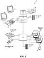
- FIG. 1is a simplified schematic block diagram of a computing device exemplary of an embodiment of the present invention.
- Computing device 10is based on a conventional Intel x 86 architecture. However, as will become apparent, the invention may easily be embodied in computing devices having a PowerPC, AMD x 86 or other architecture.
- Computing device 10includes a processor 12 , interconnected to system memory 16 and peripherals through integrated interface circuits 14 and 20 .
- Processor 12 in exemplary computing device 10is a conventional central processing unit and may for example be a microprocessor compatible with the INTEL.TM. x 86 family of microprocessors.
- Integrated interface circuits 14 and 20are often referred to as a north bridge and south bridge, respectively, and provide an interface for processor 12 to peripherals and memory.
- north bridge 14interconnects the processor 12 ; memory 16 ; a plurality of expansion slots 18 by way of a high speed interconnect bus 22 ; and south bridge 20 .
- South bridge 20in turn, interconnects lower speed peripherals and interconnects, such as disk drives by way of integrated IDE/SATA ports 24 , universal serial bus devices by way of integrated universal serial bus (USB) ports 26 ; and other peripherals by way of a lower speed interconnect bus 28 , compliant for example, with known PCI or ISA standards.
- South bridge 20may further include integrated audio components 30 , networking interfaces (not shown) and the like.
- An exemplary interconnect bus 22is the PCI express (PCIe) bus, that has a bandwidth in the gigabyte per second range, and allows data transfer reads and writes at this bandwidth.
- PCIePCI express
- current PCle bus speedsallow bi-directional data transfer at speeds of up to 266 MHz or 533 MHz, allowing data rates of up to 2.1 G bytes per second or 4.2 G bytes per second.
- north bridge 14further includes an integrated graphics adapter 34 suitable for interconnecting computing device 10 to a first display 32 in the form of a monitor, LCD panel, television or the like.
- an additional graphics adapter 52 interconnected by way of interconnect bus 22forming for example, part of peripheral expansion card 50 within expansion slots 18 on interconnect bus 22 may further be part of computing device 10 .
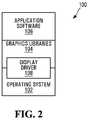
- computing device 10executes software stored within memory 16 .
- exemplary software 100includes an operation system 102 , graphics libraries 104 and application software 106 , stored within memory 16 .
- Exemplary operating systemsinclude Windows Vista, Windows XP; Windows NT 4.0 , Windows ME; Windows 98 , Windows 2000 , Windows 95 , or Linux operating systems.
- Exemplary graphics librariesinclude the Microsoft DirectX libraries and the OpenGL libraries.
- Computer memory 16 ( FIG. 1 ) and interconnected disk drivesinclude a suitable combination of random access memory, read-only memory and disk storage memory, used by device 10 to store and execute operating system and graphics adapter driver programs adapting device 10 in manners exemplary of the embodiments of the present invention.
- Exemplary software 100FIG.
- Computer readable medium 27may be an optical storage medium, a magnetic diskette, tape, ROM cartridge or the like.
- Graphics libraries 104 or operating system 102further include a graphics driver software 108 , used for low-level communication with graphics adapters 34 and 52 .
- the softwareis layered, with higher level layers using lower layers to provide certain functionality.
- Applicationsmay make use of the operating system 102 and graphics libraries 104 to render 2 D or 3 D graphics.
- Renderin this context, includes drawing, or otherwise creating a graphic image for presentation, and may for example include polygon rendering, ray-tracing, image decoding, line drawing or the like.
- software exemplary of embodiments of the present inventionmay form part of graphics libraries 104 and/or driver software 108 .
- exemplary softwaremay form part of the OpenGL library and associated drivers.
- OpenGLis more particularly detailed in The Official Guide to Learning OpenGL, Version 1.1 , the contents of which are hereby incorporated by reference.
- a person of ordinary skillwill, however, appreciate that methods exemplary of embodiments of the present invention may form part of Microsoft Direct 3 D libraries, applications (such as games) that do not use custom libraries or routine, or any other 3 D application or library.
- north bridge 14includes a high speed bus interface 36 , and memory controller 38 , interconnecting bridge 14 to interconnect bus 22 and system memory 16 .
- North bridge 14further includes integrated graphics adapter 34 , that in turn includes a graphics processor 40 , a command processor 42 and a display interface 44 .
- Graphics processor 40may take the form of a three dimensional (3D) graphics processor capable of rendering three dimensional images within a frame buffer 46 allocated within system memory 16 , and may include multiple pipelines and pipeline stages for accelerated rendering of graphics.
- 3Dthree dimensional
- command processor 42may include registers used to define a command queue 47 in memory 16 .
- Application software 106 or operating system 102uses libraries 104 to render graphics images.
- Driver software 108generates graphics processor specific commands, and places these in the command queue 47 , while also updating registers of command processor 42 to reflect the end of the queue.
- Graphics processor 42processes queued commands asynchronously, in a pipelined manner in order to, among other things, render images within frame buffer 46 .
- graphics processor 40is able to process the next command in the queue, it provides a signal to command processor 42 , which in turn fetches the next command in the queue 47 and advances the queue pointer in registers of command processor 42 .
- Display interface 44by way of memory controller 38 samples the frame buffer 46 and presents an image on one or more video output ports 48 in the form of VGA ports; composite video ports; DVI ports; HDMI; DisplayPort, or the like, for display of one or more video images on video devices such as display 32 ( FIG. 1 ), in the form of a television, monitor or the like. In this way, images rendered by graphics processor 40 in frame buffer 46 may be presented.
- display interface 44may be any suitable interface for converting data within buffer for display on a display device.
- display interface 44may take the form of a RAMDAC.
- Display interface 44is typically programmable, for example through a plurality of registers, allowing driver software 108 or similar software or graphics processor 40 to set the beginning address within memory 16 to present at its display output.
- interface 44 pixel depth (i.e. bits per pixel) and screen resolutionare typically programmable.
- two frame buffersmay be allocated.
- the buffersmay be used alternatively to more smoothly present rendered graphics.
- Display interface 44only displays contents of one of the two buffers at any time.
- the buffer being displayedis typically referred to as the front buffer.
- Graphics processor 40renders images for display to the so-called back buffer the frame buffer that is currently not being displayed by display interface 44 .
- front and back buffersare flipped: display interface 44 is programmed to present the former back buffer. In this way, transition between sequential frames rendered by graphics processor 40 may appear smooth.
- registers and frame buffer memory 46 used by adapter 34are all mapped to addresses within global memory space.
- computing device 10further includes a graphics adapter 52 formed on a peripheral expansion card 50 that may be inserted into device 10 by way of an expansion slot on high speed interconnect bus 22 , in communication with north bridge 14 , as illustrated in FIG. 1 .
- Graphics adapter 52as interconnected to north bridge 14 , is schematically illustrated in FIG. 4 .
- graphics adapter 52includes a graphics processor 54 , video memory 56 , a command processor 58 a memory controller 60 , and a display interface 62 .
- One or more ports 64 , 66allow interconnection of adapter 52 to one or more display devices, like display 68 ( FIG. 1 ).
- Command processor 58and display interface 62 function in much the same way as command processor 42 and display interface 44 , respectively.
- Graphics processor 54operates in much the same way as graphics processor 40 , in its normal mode of operation.
- Graphics adapter 52includes its own memory 56 , and a memory controller 60 to provide access to memory 56 and system memory 16 .
- Local memory 56is used to hold, among other things, one or more buffer(s) 70 for graphics adapter 52 used by graphics processor 54 , that may act as frame buffer(s).
- a command queue 57 for graphics processor 54is also established in system memory 16 .
- local memory 56is addressable at addresses within global system memory space, through memory controller 60 .
- registers used by command processor 54 and display interface 62are addressable at addresses within global address space.
- registers and frame buffer 46 used by adapter 34are mapped to global memory space.
- command processor 58 and graphics processor 54may write to frame buffer 46 and registers used by display interface 44 and command processor 42 .
- graphics processor 54in conjunction with memory controller 60 is operable to perform block transfer operations to transfer data from and to system and adapter memory 16 , 56 at memory addresses.
- integrated graphics adapter 34provides limited functionality. For example, resolution, 3 D graphics abilities, and the like of integrated graphics controller are relatively limited. Thus, integrated graphics adapter 34 typically has significantly less graphics processing ability than graphics adapter 52 . For example, adapter 34 may operate more slowly than adapter 52 , provide less features, and the like.
- integrated adapter 34 or adapter 52may, or may not, by itself allow the interconnection of multiple physical display devices, by way of multiple ports like port 48 .
- Each adaptermay be interconnected with at least one physical display.
- adapter driver software 108 loaded within memory 16causes graphics adapter 52 to act as a master (or first) graphics adapter rendering graphics for presentation at both displays 32 and 68 , and graphics adapter 34 , as a second or slave adapter.
- integrated graphics adapter 34is substantially disabled. However, components of on-board graphics adapter 34 (and in particular display interface 44 ) may still be used to drive interconnected monitors and other display devices. As such, card 50 need not include multiple display ports and display drivers. Instead, display interface 44 and its port(s) 48 may be used to drive at least one monitor or display 32 , in addition to the display 68 or displays driven by card 50 . If adapter 52 includes multiple ports (such as ports 64 , 66 ), processor 52 may additionally render images for presentation through these multiple ports. Of course, driver software 108 may also allow operation of adapter 34 in its conventional mode of operation, described above. Selection of the mode of operation of adapter 34 (and hence adapter 52 ) may be made by or through application software 106.
- driver software 108 within memory 16allocates an active frame buffer 70 and a secondary adapter buffer 72 within memory 56 of adapter 52 , as schematically depicted in FIG. 4 .
- the active frame buffer 70functions as a conventional frame buffer for adapter 52 , and thus stores frames for display on display 68 of adapter 52 .
- graphics processor 54renders 2 -D or 3 -D graphics in the active frame buffer 70 within memory 56 in a conventional manner.
- Display interface 62 of card 50converts contents of the active frame buffer 70 for display on an interconnected monitor or display device.
- active frame buffer 70may be replaced by front and rear buffers, as described above.
- Graphics processor 54further renders images for display on a display device 32 within secondary adapter frame buffer 72 .
- the contents of secondary adapter frame buffer 72are transferred to frame buffer 46 for presentation by display interface 44 of graphics adapter 34 , as detailed below.
- graphics adapter driver software 108 within memory 16performs steps S 500 depicted in FIG. 5A .
- driver software 108generates commands directing graphics processor 54 to render the secondary adapter buffer 72 of memory 56 , in steps S 502 . These commands are placed in the command queue 57 of adapter 52 and executed by graphics processor 54 , in much the same way as commands would be queued in queue 47 , as described above.
- driver software 108further generates a command (or commands) causing processor 54 to bit block transfer (BITBLT) the contents of secondary adapter frame buffer 72 within memory 56 in step S 504 , to that area of memory 16 allocated as frame buffer 46 for graphics adapter 34 .
- BITBLTbit block transfer
- Display interface 44 of graphics adapter 34has been preprogrammed to display the contents of its frame buffer 46 to an interconnected monitor or display at port 48 . Conveniently then, images displayed on displays 32 and 68 interconnected with ports 48 and port 64 are rendered or drawn by graphics processor 54 . The effects of step S 504 on buffer 72 and frame buffer 46 is illustrated in FIG. 5 B .
- steps S 600 depicted in FIG. 6 Aare performed.
- front and back frame buffersare allocated within memory 16 of adapter 52 .
- buffers 46 a and 46 bare designated as buffers 46 a and 46 b, and depicted in FIG. 6 B .
- Processor 54again renders any frame to presented by display interface 44 within secondary adapter frame buffer 72 of memory 56 as described above with reference to step S 502 , in step S 602 .
- driver software 108programs graphics processor 54 to bit block transfer (BITBLT) the contents of secondary adapter frame buffer 72 within memory 56 , to the then current back buffer within memory 16 for graphics adapter 34 in step S 604 .
- BITBLTbit block transfer
- Display interface 44 of graphics adapter 34presents the contents of it's the buffer to an interconnected monitor (i.e.
- step S 604Driver software 108 , of course, maintains the start location and status of each buffers 46 a and 46 b as front and back buffers.
- steps S 604 and S 606 on buffers 46 a and 46 bis schematically illustrated in FIG. 6 B .
- a single buffer 46 or direct programming of display interface 44 of adapter 34may cause visible tearing. That is, any time outside of the vertical blanking interval that registers of display interface 44 are reprogrammed, tearing may be visible, as display parameters are changed in the middle of the frame output by interface 44 .
- steps S 700 depicted in FIG. 7may be performed.
- front and rear buffers 46 a, 46 bare initially allocated within memory 16 used by adapter 34 .
- Processor 54again renders images for display at device 32 within buffer 72 of local memory 56 , as described above with reference to steps S 502 and S 602 .
- driver software 108within memory 16 programs graphics processor 54 to bit block transfer (BITBLT) the contents of secondary adapter frame buffer 72 within memory 56 , to the then current back buffer within memory 16 of graphics adapter 34 in step S 704 .
- Driver software 108further places a command in the command queue 47 of adapter 34 to flip front and back buffers, in step S 706 .
- registers of command processor 42are not updated by driver software 108 to reflect the pending command in command queue 47 . Instead, driver software 108 provides a command to graphics processor 54 in step S 708 to update command queue registers of command processor 42 upon completion of the bit block transfer initiated in step S 706 .
- command processor 42causes command processor 42 to provide instructions to processor 40 to flip its back to front buffer.
- Graphics processor 40executes the queued command to flip back and front buffers of adapter 34 (i.e. by reprogramming registers of display interface 44 to present the contents of its previous back buffer to an interconnected monitor or display at port 48 ).
- steps S 800 depicted in FIG. 8are performed. Again, front and back buffers are initially allocated within memory 16 of adapter 34 . Processor 54 again renders images for display 32 within buffer 72 of local memory 56 , as described above.
- Driver software 108further places a command in queue 47 of adapter 34 to cause graphics processor 40 to bit block transfer (BITBLT) the contents of the secondary frame buffer 72 within memory 56 , to that area of system memory 16 allocated as the current back frame buffer for graphics adapter 34 .
- Driver software 108also places a command in queue 47 to cause graphics processor 40 to flip front and back buffers of adapter 34 by programming display interface 44 to use the rear buffer as front buffer.
- registers of command processor 42 defining the queue pointerare not updated until a frame has been rendered in buffer 72 .
- graphics processor 54provides a command to update command registers defining the queue pointer for command processor 42 to reflect the two pending commands within the command queue of adapter 34 .
- Graphics processor 40executes the queued commands to bit block transfer the contents of buffer 72 to its back buffer and flip its back and front buffers (i.e. by reprogramming registers of display interface 44 to present the contents of its previous back buffer to an interconnected monitor or display at port 48 ).
- a slave graphics adaptermay be used to display images created in one frame buffer.
- Device electronics and ports required to drive additional displaysmay be provided by slave graphics adapter 34 .
- electronics included in the slave graphics controllermay be effectively utilized to allow driving of multiple displays.
- buffers 70 and 72may be used to define a single surface on which application software 106 may render single graphic images to be displayed across two or more displays 48 and 64 , interconnected with graphics adapters 52 and 34 .
- Driver software 108may accordingly report an available screen size to application software 106 , equal to the size of buffer 70 and buffer 72 .
- buffer 70has a resolution of m.sub. 1 xn
- buffer 72has a resolution of m.sub. 2 xn
- driver software 108may report an available screen size of (m.sub. 1 +m.sub. 2 )xn to an application of application software 106 .
- Rendering by driver software 108is simplified if buffers 70 and 72 occupy adjacent (m.sub. 1 +m.sub.
- Application software 106may, in turn use driver software 108 to cause graphics processor 40 to render larger images having a resolution of (m.sub. 1 +m.sub. 2 )xn pixels making up the surface defined by buffers 70 and 72 .
- Buffers 70 and 72thus store image pairs, with each image of the pair forming a portion of the larger image rendered by the application.
- driver software 108may transfer the image in buffer 72 to frame buffer 46 , for display on display 32 , in accordance with steps S 500 , S 600 , S 700 or S 800 described above.
- the image in buffer 70may be displayed on display 68 in normal fashion.
- An end user viewing displays 32 and 68 side by siderecognizes the larger image rendered by application 106 .
- application 106 in the form of a gamemay take advantage of multiple displays, without requiring modification.
- Steps S 602 , S 604 , S 702 , S 704 , or steps S 802 , S 704could accordingly be modified to bit block transfer the buffer holding the just completed image to the back buffer 46 a or 46 b.
- existing application software 106need not be modified. Instead, the application software may simply rely on the reported larger screen size.
- Driver software 108causes the rendering of surfaces across multiple displays.
- the slave graphics adaptercould easily be another graphics adapter in communication with graphics adapter 52 by way of a bus having sufficient bandwidth to allow transfer of graphics frames into the slave frame buffer(s).
- the slave graphics processorcould be formed as another PCle compliant expansion card. So, for example, as graphics cards are upgraded, older expansion cards may still be used for their ability to drive interconnected displays.
- the interconnect busneed not be a PCle interconnect bus, but could be any other suitable bus having a bandwidth allowing transfer of data between frame buffers at a rate equal to the refresh rate used by display interface 44 .
- frame buffers 46and front and back buffers 46 a and 46 b
- frame buffers 46have been described as being formed in system memory 16 , they could easily be formed as part of memory local to adapter 34 .
- rendering across bus 22may allow a graphics adapter (or subsystem) interconnected by high speed bus 22 to take the place of an integrated adapter/subsystem.
- FIG. 9is a simplified block diagrams exemplary of a portion of a computing device 10' exemplary of another embodiment.
- Computing device 10'is detailed in US Patent Application No. 11/421,005 .
- device 10'includes two graphics subsystem 30' and 40' .
- Graphics subsystem 30'includes a graphics engine/processor 32' , a memory controller 72' , a display interface 74' and a bus interface 78' .
- a second graphics subsystem 40'is in communication with graphics subsystem 30' , by way of high speed bus 22' , such as the PCle bus .
- Graphics subsystem 40'includes its own graphics engine/processor 42' ; memory controller 52' ; display interface 54' .
- Graphics subsystem 40'is further in communication with graphics memory 50' .
- subsystem 40'is adapted to render graphics to memory 14' , across bus 22' .
- Device 10'may conveniently be formed as a portable computing device in the form of a laptop or smaller computing device.
- a single housingmay contain a DC power source, display 26' and the above mentioned motherboard and components.
- the second graphics subsystem 40'may be added to a single housing that houses the remainder of the computing device, or may form part of a docking station that only forms part of device 10' , when device 10' is physically interconnected thereto.
- Device 10'may be operated in at least two power consumption modes: a higher power consumption mode and a lower power consumption mode.
- the higher power modemay be assumed when device 10' is powered by a power source connected to an AC(mains) supply; the lower power consumption mode may be assumed when device 10' is powered by a DC power source using one or more batteries, fuel cells, or the like.
- power consumption modesmay be user selected, software controlled, based on for example, user preferences, types of software applications being executed, battery levels, and the like, or otherwise chosen.
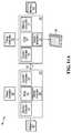
- FIG. 10depicts software blocks S800' , that may be performed by a central processor (like processor 12 - FIG. 1 ) under control of software within system memory of device 10' .
- Blocks S800'may be performed each time device 10' undergoes a state change, for which subsystems 30' and 40' should be configured accordingly.
- the softwaredetermines whether device 10' should assume its higher power consumption mode, or its lower power consumption mode.
- blocks S804'-S810'are executed.
- graphics subsystem 40'is placed in its full operational (high power consumption) mode, if it is not already in this mode. This may be performed by providing an appropriate signal to power controller 60' , through the driver controlling graphics subsystem 40' .
- graphics subsystem 40'is enabled in blocks S806 and S808 . Again, this may be performed by logically disabling any display interconnected associated with graphics subsystem 30' in block S804 , and logically enabling the display connected with graphics subsystem 40' , in block S808 .
- Blocks S806 and S808may again be performed, by appropriate operating system API calls, such as the EnumDisplayDevices() and ChangeDisplaySettingsEX() calls described in the 11/421,005 patent application, or through direct communication with hardware.
- graphics subsystem 40'no physical display is connected to graphics subsystem 40' .
- Driver software controlling operation of graphics subsystem 40'is configured to render images in buffer 14' of graphics subsystem 30' instead of within associated memory 50' in step S810' .
- high speed bus 22'embodied, for example, as the PCle bus
- renderingis possible across bus 22' , owing in part to transfer speeds enabled by the bus.
- the renderingmay be direct into the frame buffer across the bus, primitive by primitive, thus transferring the rendered image across bus 22' . This may be facilitated by allocating buffer 14' in memory accessible by subsystem 40' and providing the driver software for subsystem 40' with the address of buffer 14' . Alternatively, as will become apparent, the frames may be rendered in one buffer, and transferred by direct memory access or the like across bus 22' .
- the driver for graphics subsystem 30'is further configured to cause display interface 74' of graphics subsystem 30' to sample the frame buffer in memory 14' , so as to present the image rendered by graphics subsystem 40' in the frame buffer in memory 14' at interconnected display 26' .
- the driver for graphics subsystem 30'may direct graphics engine 32' of graphics subsystem 30' to remain substantially dormant or idle. This mode of operation is schematically depicted in FIG. 11A with only the active blocks of graphics subsystem 40' and graphics subsystem 30' , crosshatched.
- memory 50' and display interface 54'are not used. As such, these functional blocks could be eliminated from subsystem 40' allowing cost reduction.
- the resulting subsystem 40'need not include a display interface and would lack memory defining a frame buffer local to subsystem 40' .
- Producing such a graphics subsystemmay be beneficial, as subsystem 40' could be produced to complement the functionality provided by subsystem 30' .
- subsystemcould provide a graphics engine 42' that provides 3 D graphics or video decoding capabilities. Graphics engine 32' may not include these capabilities.
- 2 D graphics abilities offered by graphics engine 32'need not be included in subsystem 40' . Consumers, in turn could add graphics subsystem 30' only when additional functionality is needed.
- blocks S812' - S818'are executed.
- graphics subsystem 40'is partially or completely disabled and placed in its low power consumption mode, and rendering is again performed by graphics subsystem 30' .
- any display interconnected associated with graphics subsystem 30'may be enabled in block S812'
- any display physically connected with graphics subsystem 40'may be logically disabled in block S814' .
- driver software controlling operation of graphics subsystem 30'is again configured to cause graphics subsystem 30' to render images in memory 14' .
- Display interface 74'continues to sample memory 14' to present images on display 26' interconnected with port 78' .
- processor 12'first provides a suitable signal to power controller 60' in block S818' , placing graphics subsystem 40' in its low power state.
- a power controller(not shown) disconnects power to graphics subsystem 40' or places graphics subsystem 40' into a lower power sleep mode.
- voltagesare throttled, and/or all or parts of graphics subsystem 40' are powered down and/or selected clocks used by graphics subsystem 40' are slowed.
- the graphics engine 42' of graphics subsystem 40'remains idle or substantially idle (e.g. it may be slowed, disable or powered down).
- This mode of operationis schematically depicted in FIG. 9B with only the active functional blocks of adapter 40' and graphics subsystem 30' , crosshatched.
- the inactive/idle functional blocksmay be entirely disabled, or operated at reduced voltages or clock speeds.
- portions of graphics subsystem 30'could be disabled when graphics engine 32' is not in use. This could be facilitated by placing graphics engine 32' and other components on one or more voltage islands that may be disabled by way of a GPIO or similar circuit, any time graphics subsystem 40' is responsible for rendering images.
- both graphics subsystem 30' and graphics subsystem 40'could render to memory 14' or memory 50' .
- the two graphics subsystems 30' and 40'may operate in concert, each rendering an alternate frame in memory 14' or rendering an alternate portion (e.g. scan-line) of each frame in memory 14' .
- additional displaysmay be connected to graphics subsystems 30' and 40' allowing concurrent use of multiple displays in the high power consumption modes, as detailed above.
- display interface 54'could be used to drive a second display.
- device 10'Upon transition to a lower power consumption mode, device 10' could be configured to operate as depicted in FIG. 11B .
- device 10'could include multiple additional graphics subsystems connected to bus 22' (or 22 ), all of which could be active in the high power consumption mode, and render graphics through display interface 74' of graphics subsystem 30' . Upon transition to the lower power consumption mode, these could be disabled and rendering could be left to graphics engine 32' of graphics subsystem 30' .
- computing device 10'may include a direct memory access (DMA) controller 90 .
- DMA controller 90may transfer data from memory 50' to memory 14' .
- graphics subsystem 40'could render images to memory 50' . These rendered images could then be transferred by DMA controller 90 to a frame buffer in memory 14' .
- DMA controller 90'could form part of graphics subsystem 30' or 40' (for example as DMA engines of graphics engines 32' or 42' ), or be otherwise located in computing device 10' .
- Datamay be transferred across bus 20' or otherwise directly from memory 50' to memory 14' .
- Display interface 74'would continue operating as disclosed above, sampling the frame buffer in memory 14' to present the rendered image on display 26' .
- active blocks of device 10' of FIG. 10in its higher power consumption mode are illustrated in crosshatch in FIG. 12 .
Landscapes
- Engineering & Computer Science (AREA)
- Theoretical Computer Science (AREA)
- Physics & Mathematics (AREA)
- General Physics & Mathematics (AREA)
- Computer Hardware Design (AREA)
- Computer Graphics (AREA)
- Human Computer Interaction (AREA)
- General Engineering & Computer Science (AREA)
- Controls And Circuits For Display Device (AREA)
- Digital Computer Display Output (AREA)
- Information Transfer Systems (AREA)
Description
- The present invention relates generally to computing devices, and more particularly to a computing device including graphics processors interconnected by a high speed peripheral bus.
- In recent years, computer hardware has become increasingly integrated. Computer peripherals are often formed as part of an integrated chipset that cooperates with a central processor. Often, computer audio, graphics adapters and interfaces form part of the integrated chipsets. Such integration reduces costs and size of the computing devices.
- At the same time, graphics processors are steadily evolving to provide enhanced performance and features. Leading graphics processors are nearly as complex as central processors. Thus, despite trends in integration, high performance graphics processors are still typically formed on peripheral cards. Integrated graphics processors, are by comparison, relatively simple and do not provide the features or performance of the high performance, graphics processors formed on peripheral cards. In the presence of an add-on peripheral card, integrated graphics components when present, are typically redundant and therefore disabled.
- Similarly, as graphics adapters, whether integrated or external, are upgraded there is often no role for less powerful adapters, and these are disposed of or disabled.
- United States patent application publication no.
2006/0267987 discloses a master/slave graphics adapter arrangement according to which a computing device includes first and second graphics adapters. A graphics processor of the first graphics adapter acts as a master graphics processor, while the second graphics adapter acts as a slave. The master graphics processor renders graphics to be displayed on multiple separate displays within frame buffer memory of the first graphics adapter. Images to be displayed on one of the separate displays are transferred from frame buffer memory of the first graphics adapter to frame buffer memory of the second graphics adapter. Other documents in this technical field areUS 2005/285863 andUS 5 896 141 . - Accordingly, there remains a need to reduce component redundancy.
- In accordance with an aspect of the present invention, graphics generated by one graphics processor are transferred across a high speed expansion/interconnect bus to a frame buffer. The rendered frames from the frame buffer are presented on a display by way of a display interface in communication with the frame buffer.
- Conveniently, the display interface of another existing (e.g. integrated) graphics adapter/subsystem may be used to present the rendered frames on an interconnected display.
- In this way the graphics processor may form part of a graphics adapter that need not include a display interface or possibly even a frame buffer. Likewise, the graphics processor may be replaced with a more current graphics processor.
- The graphics processor may form part of a graphics adapter contained on a peripheral expansion card.
- In accordance with a first aspect there is provided a method of operating a computing device according to claim 1.
- In accordance with another aspect of the present invention, there is provided a graphics subsystem for connection to a host computing device according to claim 6.
- A third aspect of the present invention provides a computing device comprising the graphics subsystem and the host device according to claim 8.
- In the figures,
FIG. 1 is a simplified block diagram of a computing device, exemplary of an embodiment of the present invention;FIG. 2 is a simplified logical block diagram of software at the computing device ofFIG. 1 ;FIG. 3 is a simplified block diagram of a portion of the computing device ofFIG. 1 ;FIG. 4 is a further schematic block diagram of a portion of the computing device ofFIG. 1 FIG. 5A is a flow chart illustrating steps performed at the computing device ofFIG. 1 ,FIG. 5B schematically depicts the effects of steps ofFIG. 5A on components of the device ofFIG. 1 ;FIG. 6A is a flow chart illustrating steps performed at the computing device ofFIG. 1 FIG. 6B schematically depicts the effects of steps ofFIG. 6A on components of the device ofFIG. 1 ;FIGS. 7 and8 are flow charts illustrating steps performed at the computing device ofFIG. 1 FIG. 9 is a further partial simplified schematic block diagram of portions of a computing device,FIG. 10 , is a flow chart detailing steps performed by software at the device ofFIG. 9 , andFIG. 11A ,11B are simplified block diagrams illustrating operation of the device ofFIG. 9 ; andFIG. 12 is a further partial simplified schematic block diagram of portions of a computing device,FIG.1 is a simplified schematic block diagram of a computing device exemplary of an embodiment of the present invention.Computing device 10 is based on a conventional Intel x86 architecture. However, as will become apparent, the invention may easily be embodied in computing devices having a PowerPC, AMD x86 or other architecture.Computing device 10 includes aprocessor 12, interconnected tosystem memory 16 and peripherals through integratedinterface circuits Processor 12 inexemplary computing device 10 is a conventional central processing unit and may for example be a microprocessor compatible with the INTEL.TM. x86 family of microprocessors.Integrated interface circuits processor 12 to peripherals and memory. As illustrated,north bridge 14 interconnects theprocessor 12;memory 16; a plurality ofexpansion slots 18 by way of a highspeed interconnect bus 22; andsouth bridge 20. Southbridge 20 in turn, interconnects lower speed peripherals and interconnects, such as disk drives by way of integrated IDE/SATA ports 24, universal serial bus devices by way of integrated universal serial bus (USB)ports 26; and other peripherals by way of a lowerspeed interconnect bus 28, compliant for example, with known PCI or ISA standards. Southbridge 20 may further include integratedaudio components 30, networking interfaces (not shown) and the like.- An
exemplary interconnect bus 22 is the PCI express (PCIe) bus, that has a bandwidth in the gigabyte per second range, and allows data transfer reads and writes at this bandwidth. For example, current PCle bus speeds allow bi-directional data transfer at speeds of up to266 MHz or533 MHz, allowing data rates of up to2.1 G bytes per second or4.2 G bytes per second. - In the depicted
embodiment north bridge 14 further includes anintegrated graphics adapter 34 suitable for interconnectingcomputing device 10 to afirst display 32 in the form of a monitor, LCD panel, television or the like. - As detailed below, an
additional graphics adapter 52 interconnected by way ofinterconnect bus 22, forming for example, part ofperipheral expansion card 50 withinexpansion slots 18 oninterconnect bus 22 may further be part ofcomputing device 10. - In the depicted embodiment,
computing device 10 executes software stored withinmemory 16. As illustrated inFIG.2 ,exemplary software 100 includes anoperation system 102,graphics libraries 104 andapplication software 106, stored withinmemory 16. Exemplary operating systems include Windows Vista, Windows XP; Windows NT4.0, Windows ME; Windows98, Windows2000, Windows95, or Linux operating systems. Exemplary graphics libraries include the Microsoft DirectX libraries and the OpenGL libraries. Computer memory16 (FIG.1 ) and interconnected disk drives (not shown) include a suitable combination of random access memory, read-only memory and disk storage memory, used bydevice 10 to store and execute operating system and graphics adapter driverprograms adapting device 10 in manners exemplary of the embodiments of the present invention. Exemplary software100 (FIG.2 ) could, for example, be stored in read-only memory or loaded from an external peripheral such as a disk drive in communication with IDE/SATA ports 24. Computerreadable medium 27 may be an optical storage medium, a magnetic diskette, tape, ROM cartridge or the like. Graphics libraries 104 oroperating system 102 further include agraphics driver software 108, used for low-level communication withgraphics adapters operating system 102 andgraphics libraries 104 to render2D or3D graphics. Render, in this context, includes drawing, or otherwise creating a graphic image for presentation, and may for example include polygon rendering, ray-tracing, image decoding, line drawing or the like. As will become, apparent, software exemplary of embodiments of the present invention may form part ofgraphics libraries 104 and/ordriver software 108. In the exemplified embodiment, exemplary software may form part of the OpenGL library and associated drivers. OpenGL is more particularly detailed in The Official Guide to Learning OpenGL, Version1.1, the contents of which are hereby incorporated by reference. A person of ordinary skill will, however, appreciate that methods exemplary of embodiments of the present invention may form part of Microsoft Direct3D libraries, applications (such as games) that do not use custom libraries or routine, or any other3D application or library.- A further simplified block diagram of portions of exemplary computing device10 (and particularly north bridge14) depicting
integrated graphics adapter 34 is illustrated inFIG.3 . As illustrated,north bridge 14 includes a highspeed bus interface 36, andmemory controller 38, interconnectingbridge 14 to interconnectbus 22 andsystem memory 16.North bridge 14 further includesintegrated graphics adapter 34, that in turn includes agraphics processor 40, acommand processor 42 and adisplay interface 44. Graphics processor 40 may take the form of a three dimensional (3D) graphics processor capable of rendering three dimensional images within aframe buffer 46 allocated withinsystem memory 16, and may include multiple pipelines and pipeline stages for accelerated rendering of graphics.- In normal, single monitor operation, commands are passed to
graphics processor 40 bycommand processor 42, in a conventional manner. For example,command processor 42 may include registers used to define acommand queue 47 inmemory 16.Application software 106 oroperating system 102 useslibraries 104 to render graphics images.Driver software 108 generates graphics processor specific commands, and places these in thecommand queue 47, while also updating registers ofcommand processor 42 to reflect the end of the queue.Graphics processor 42 processes queued commands asynchronously, in a pipelined manner in order to, among other things, render images withinframe buffer 46. Asgraphics processor 40 is able to process the next command in the queue, it provides a signal to commandprocessor 42, which in turn fetches the next command in thequeue 47 and advances the queue pointer in registers ofcommand processor 42. Display interface 44, by way ofmemory controller 38 samples theframe buffer 46 and presents an image on one or morevideo output ports 48 in the form of VGA ports; composite video ports; DVI ports; HDMI; DisplayPort, or the like, for display of one or more video images on video devices such as display32 (FIG.1 ), in the form of a television, monitor or the like. In this way, images rendered bygraphics processor 40 inframe buffer 46 may be presented.- As will be appreciated
display interface 44 may be any suitable interface for converting data within buffer for display on a display device. For example,display interface 44 may take the form of a RAMDAC.Display interface 44 is typically programmable, for example through a plurality of registers, allowingdriver software 108 or similar software orgraphics processor 40 to set the beginning address withinmemory 16 to present at its display output. As well, interface44 pixel depth (i.e. bits per pixel) and screen resolution are typically programmable. - As will be appreciated, instead of allocating a
single frame buffer 46 withinmemory 16, two frame buffers may be allocated. The buffers may be used alternatively to more smoothly present rendered graphics.Display interface 44 only displays contents of one of the two buffers at any time. The buffer being displayed is typically referred to as the front buffer.Graphics processor 40 renders images for display to the so-called back buffer the frame buffer that is currently not being displayed bydisplay interface 44. At the completion of rendering a frame, front and back buffers are flipped:display interface 44 is programmed to present the former back buffer. In this way, transition between sequential frames rendered bygraphics processor 40 may appear smooth. - Notably, registers and
frame buffer memory 46 used byadapter 34 are all mapped to addresses within global memory space. - Exemplary of the present invention, however,
computing device 10 further includes agraphics adapter 52 formed on aperipheral expansion card 50 that may be inserted intodevice 10 by way of an expansion slot on highspeed interconnect bus 22, in communication withnorth bridge 14, as illustrated inFIG.1 .Graphics adapter 52, as interconnected tonorth bridge 14, is schematically illustrated inFIG.4 . As illustrated,graphics adapter 52 includes agraphics processor 54,video memory 56, a command processor58 amemory controller 60, and adisplay interface 62. One ormore ports adapter 52 to one or more display devices, like display68 (FIG.1 ). Command processor 58, anddisplay interface 62 function in much the same way ascommand processor 42 anddisplay interface 44, respectively.Graphics processor 54 operates in much the same way asgraphics processor 40, in its normal mode of operation.Graphics adapter 52 includes itsown memory 56, and amemory controller 60 to provide access tomemory 56 andsystem memory 16.Local memory 56 is used to hold, among other things, one or more buffer(s)70 forgraphics adapter 52 used bygraphics processor 54, that may act as frame buffer(s). Acommand queue 57 forgraphics processor 54 is also established insystem memory 16.- Again,
local memory 56 is addressable at addresses within global system memory space, throughmemory controller 60. As well, registers used bycommand processor 54 anddisplay interface 62 are addressable at addresses within global address space. As already noted, registers andframe buffer 46 used byadapter 34 are mapped to global memory space. Thus,command processor 58 andgraphics processor 54 may write to framebuffer 46 and registers used bydisplay interface 44 andcommand processor 42. - Additionally,
graphics processor 54, in conjunction withmemory controller 60 is operable to perform block transfer operations to transfer data from and to system andadapter memory - In an effort to provide economical integrated components,
integrated graphics adapter 34 provides limited functionality. For example, resolution,3D graphics abilities, and the like of integrated graphics controller are relatively limited. Thus,integrated graphics adapter 34 typically has significantly less graphics processing ability thangraphics adapter 52. For example,adapter 34 may operate more slowly thanadapter 52, provide less features, and the like. - Now, integrated
adapter 34 oradapter 52 may, or may not, by itself allow the interconnection of multiple physical display devices, by way of multiple ports likeport 48. Each adapter, however, may be interconnected with at least one physical display. So, exemplary of embodiments of the present invention,adapter driver software 108 loaded withinmemory 16causes graphics adapter 52 to act as a master (or first) graphics adapter rendering graphics for presentation at bothdisplays graphics adapter 34, as a second or slave adapter. - As will become apparent, in this master/slave mode of operation,
integrated graphics adapter 34 is substantially disabled. However, components of on-board graphics adapter34 (and in particular display interface44) may still be used to drive interconnected monitors and other display devices. As such,card 50 need not include multiple display ports and display drivers. Instead,display interface 44 and its port(s)48 may be used to drive at least one monitor ordisplay 32, in addition to thedisplay 68 or displays driven bycard 50. Ifadapter 52 includes multiple ports (such asports 64,66),processor 52 may additionally render images for presentation through these multiple ports. Of course,driver software 108 may also allow operation ofadapter 34 in its conventional mode of operation, described above. Selection of the mode of operation of adapter34 (and hence adapter52) may be made by or throughapplication software 106. - Specifically, in the master/slave mode of operation, exemplary of embodiments of the present invention,
driver software 108 withinmemory 16 allocates anactive frame buffer 70 and asecondary adapter buffer 72 withinmemory 56 ofadapter 52, as schematically depicted inFIG.4 . Theactive frame buffer 70 functions as a conventional frame buffer foradapter 52, and thus stores frames for display ondisplay 68 ofadapter 52. As such,graphics processor 54 renders2-D or3-D graphics in theactive frame buffer 70 withinmemory 56 in a conventional manner.Display interface 62 ofcard 50 converts contents of theactive frame buffer 70 for display on an interconnected monitor or display device. Optionally,active frame buffer 70 may be replaced by front and rear buffers, as described above. Graphics processor 54 further renders images for display on adisplay device 32 within secondaryadapter frame buffer 72. At the conclusion of rendering a frame within secondaryadapter frame buffer 72, the contents of secondaryadapter frame buffer 72 are transferred to framebuffer 46 for presentation bydisplay interface 44 ofgraphics adapter 34, as detailed below.- In a first embodiment, graphics
adapter driver software 108 withinmemory 16 performs steps S500 depicted inFIG. 5A . Specifically,driver software 108 generates commands directinggraphics processor 54 to render thesecondary adapter buffer 72 ofmemory 56, in steps S502. These commands are placed in thecommand queue 57 ofadapter 52 and executed bygraphics processor 54, in much the same way as commands would be queued inqueue 47, as described above. Once the frame is rendered,driver software 108 further generates a command (or commands) causingprocessor 54 to bit block transfer (BITBLT) the contents of secondaryadapter frame buffer 72 withinmemory 56 in step S504, to that area ofmemory 16 allocated asframe buffer 46 forgraphics adapter 34. Display interface 44 ofgraphics adapter 34, in turn, has been preprogrammed to display the contents of itsframe buffer 46 to an interconnected monitor or display atport 48. Conveniently then, images displayed ondisplays ports 48 andport 64 are rendered or drawn bygraphics processor 54. The effects of step S504 onbuffer 72 andframe buffer 46 is illustrated inFIG.5B .- In a second embodiment, steps S600 depicted in
FIG.6A are performed. Initially, front and back frame buffers are allocated withinmemory 16 ofadapter 52. For convenience these are designated as buffers46a and46b, and depicted inFIG.6B .Processor 54 again renders any frame to presented bydisplay interface 44 within secondaryadapter frame buffer 72 ofmemory 56 as described above with reference to step S502, in step S602. - At the conclusion of rendering a frame for display on
device 32,driver software 108programs graphics processor 54 to bit block transfer (BITBLT) the contents of secondaryadapter frame buffer 72 withinmemory 56, to the then current back buffer withinmemory 16 forgraphics adapter 34 in step S604. Upon completion of the BITBLT,driver programs processor 54 to program registers ofdisplay interface 44 to flip the back buffer and front buffer of adapter34 (i.e. use the back buffer as the front buffer), in step S606. This may be done by directly reprogramming the register ofdisplay interface 44 identifying the start address used bydisplay interface 44 for presentation of data.Display interface 44 ofgraphics adapter 34, in turn, presents the contents of it's the buffer to an interconnected monitor (i.e. display68) atport 48. The previous front buffer, in turn, is now used as back buffer foradapter 34, and the next frame rendered byprocessor 54 for display ondisplay 32 will initially be transferred to this back buffer in step S604.Driver software 108, of course, maintains the start location and status of each buffers46a and46b as front and back buffers. The effect of steps S604 and S606 on buffers46a and46b is schematically illustrated inFIG.6B . - Without synchronization, use of a
single buffer 46 or direct programming ofdisplay interface 44 ofadapter 34 may cause visible tearing. That is, any time outside of the vertical blanking interval that registers ofdisplay interface 44 are reprogrammed, tearing may be visible, as display parameters are changed in the middle of the frame output byinterface 44. - Thus, in yet a third embodiment, steps S700 depicted in
FIG.7 may be performed. Again, front and rear buffers46a,46b are initially allocated withinmemory 16 used byadapter 34.Processor 54 again renders images for display atdevice 32 withinbuffer 72 oflocal memory 56, as described above with reference to steps S502 and S602. - At the completion of rendering a frame for display on
display 32,driver software 108 withinmemory 16programs graphics processor 54 to bit block transfer (BITBLT) the contents of secondaryadapter frame buffer 72 withinmemory 56, to the then current back buffer withinmemory 16 ofgraphics adapter 34 in step S704.Driver software 108 further places a command in thecommand queue 47 ofadapter 34 to flip front and back buffers, in step S706. However, registers ofcommand processor 42 are not updated bydriver software 108 to reflect the pending command incommand queue 47. Instead,driver software 108 provides a command tographics processor 54 in step S708 to update command queue registers ofcommand processor 42 upon completion of the bit block transfer initiated in step S706. This, in turn causescommand processor 42 to provide instructions toprocessor 40 to flip its back to front buffer.Graphics processor 40, in turn executes the queued command to flip back and front buffers of adapter34 (i.e. by reprogramming registers ofdisplay interface 44 to present the contents of its previous back buffer to an interconnected monitor or display at port48). - In yet a fourth embodiment, steps S800 depicted in
FIG.8 are performed. Again, front and back buffers are initially allocated withinmemory 16 ofadapter 34.Processor 54 again renders images fordisplay 32 withinbuffer 72 oflocal memory 56, as described above. Driver software 108 further places a command inqueue 47 ofadapter 34 to causegraphics processor 40 to bit block transfer (BITBLT) the contents of thesecondary frame buffer 72 withinmemory 56, to that area ofsystem memory 16 allocated as the current back frame buffer forgraphics adapter 34.Driver software 108 also places a command inqueue 47 to causegraphics processor 40 to flip front and back buffers ofadapter 34 byprogramming display interface 44 to use the rear buffer as front buffer. However, registers ofcommand processor 42 defining the queue pointer are not updated until a frame has been rendered inbuffer 72.- So, at the conclusion of rendering a frame for
display 32,graphics processor 54 provides a command to update command registers defining the queue pointer forcommand processor 42 to reflect the two pending commands within the command queue ofadapter 34.Graphics processor 40, in turn executes the queued commands to bit block transfer the contents ofbuffer 72 to its back buffer and flip its back and front buffers (i.e. by reprogramming registers ofdisplay interface 44 to present the contents of its previous back buffer to an interconnected monitor or display at port48). - As will now be appreciated, the above described embodiments allow a master graphics processor to assume responsibility for drawing two or three dimensional graphics images on multiple independent frame buffers. A slave graphics adapter may be used to display images created in one frame buffer. Device electronics and ports required to drive additional displays may be provided by
slave graphics adapter 34. In this way, electronics included in the slave graphics controller may be effectively utilized to allow driving of multiple displays. - Conveniently, buffers70 and72 may be used to define a single surface on which
application software 106 may render single graphic images to be displayed across two ormore displays graphics adapters Driver software 108 may accordingly report an available screen size toapplication software 106, equal to the size ofbuffer 70 andbuffer 72. Thus, ifbuffer 70 has a resolution of m.sub.1xn andbuffer 72 has a resolution of m.sub.2xn,driver software 108 may report an available screen size of (m.sub.1+m.sub.2)xn to an application ofapplication software 106. Rendering bydriver software 108 is simplified ifbuffers memory 56.Application software 106 may, in turnuse driver software 108 to causegraphics processor 40 to render larger images having a resolution of (m.sub.1+m.sub.2)xn pixels making up the surface defined bybuffers Buffers driver software 108 may transfer the image inbuffer 72 to framebuffer 46, for display ondisplay 32, in accordance with steps S500, S600, S700 or S800 described above. The image inbuffer 70 may be displayed ondisplay 68 in normal fashion. An end user viewing displays32 and68 side by side recognizes the larger image rendered byapplication 106. As will be appreciated,application 106 in the form of a game may take advantage of multiple displays, without requiring modification. - If front and back buffers are used for
display 68, two different buffers may be allocated and used in place ofbuffer 72, to ensure that the buffer holding the surface portion to be displayed ondisplay 32 is adjacent inmemory 56 to the buffer in which the surface portion to be displayed ondisplay 68 is being rendered. Steps S602, S604, S702, S704, or steps S802, S704 could accordingly be modified to bit block transfer the buffer holding the just completed image to the back buffer46a or46b. Conveniently, existingapplication software 106 need not be modified. Instead, the application software may simply rely on the reported larger screen size.Driver software 108 causes the rendering of surfaces across multiple displays. - As will now also be appreciated, although the depicted embodiment utilizes an integrated graphics controller as a slave graphics adapter, the slave graphics adapter could easily be another graphics adapter in communication with
graphics adapter 52 by way of a bus having sufficient bandwidth to allow transfer of graphics frames into the slave frame buffer(s). As such, the slave graphics processor could be formed as another PCle compliant expansion card. So, for example, as graphics cards are upgraded, older expansion cards may still be used for their ability to drive interconnected displays. Similarly, the interconnect bus need not be a PCle interconnect bus, but could be any other suitable bus having a bandwidth allowing transfer of data between frame buffers at a rate equal to the refresh rate used bydisplay interface 44. Likewise, although frame buffers46 (and front and back buffers46a and46b) have been described as being formed insystem memory 16, they could easily be formed as part of memory local toadapter 34. - In yet another alternate embodiment rendering across
bus 22, may allow a graphics adapter (or subsystem) interconnected byhigh speed bus 22 to take the place of an integrated adapter/subsystem. - To this end,
FIG. 9 is a simplified block diagrams exemplary of a portion of acomputing device 10' exemplary of another embodiment.Computing device 10' is detailed inUS Patent Application No. 11/421,005 - Briefly, however,
device 10' includes two graphics subsystem30' and40'. Graphics subsystem30' includes a graphics engine/processor32', a memory controller72', a display interface74' and a bus interface78'. A second graphics subsystem40' is in communication with graphics subsystem30', by way of high speed bus22',such as the PCle bus. Graphics subsystem40' includes its own graphics engine/processor42'; memory controller52'; display interface54'. Graphics subsystem40' is further in communication with graphics memory50'. As will become apparent, subsystem40' is adapted to render graphics to memory14', across bus22'. Device 10' may conveniently be formed as a portable computing device in the form of a laptop or smaller computing device. As such, a single housing may contain a DC power source, display26' and the above mentioned motherboard and components. The second graphics subsystem40' may be added to a single housing that houses the remainder of the computing device, or may form part of a docking station that only forms part ofdevice 10', whendevice 10' is physically interconnected thereto.Device 10' may be operated in at least two power consumption modes: a higher power consumption mode and a lower power consumption mode. In the depicted embodiments,device 10' the higher power mode may be assumed whendevice 10' is powered by a power source connected to an AC(mains) supply; the lower power consumption mode may be assumed whendevice 10' is powered by a DC power source using one or more batteries, fuel cells, or the like. Alternatively, power consumption modes may be user selected, software controlled, based on for example, user preferences, types of software applications being executed, battery levels, and the like, or otherwise chosen.- The organization of software controlling operation of
device 10' is disclosed inU.S. Patent Application No. 11/421,005 , and shares similarity tosoftware 100, described above. - Portions of the software controlling operation of
device 10' asdevice 10' transitions between high and low power consumption states. SpecificallyFIG. 10 depicts software blocksS800', that may be performed by a central processor (like processor12 -FIG. 1 ) under control of software within system memory ofdevice 10'. BlocksS800' may be performed eachtime device 10' undergoes a state change, for which subsystems30' and40' should be configured accordingly. As illustrated, in blockS802' the software determines whetherdevice 10' should assume its higher power consumption mode, or its lower power consumption mode. - When
device 10' is to resume (or transition) to its high power consumption mode, blocksS804'-S810' are executed. In blockS804 graphics subsystem40' is placed in its full operational (high power consumption) mode, if it is not already in this mode. This may be performed by providing an appropriate signal to power controller60', through the driver controlling graphics subsystem40'. Next, graphics subsystem40' is enabled in blocksS806 andS808. Again, this may be performed by logically disabling any display interconnected associated with graphics subsystem30' in blockS804, and logically enabling the display connected with graphics subsystem40', in blockS808. BlocksS806 andS808 may again be performed, by appropriate operating system API calls, such as the EnumDisplayDevices() and ChangeDisplaySettingsEX() calls described in the 11/421,005 patent application, or through direct communication with hardware. - Notably, no physical display is connected to graphics subsystem40'. Driver software controlling operation of graphics subsystem40' is configured to render images in buffer14' of graphics subsystem30' instead of within associated memory50' in stepS810'. Conveniently, in the presence of high speed bus22' (embodied, for example, as the PCle bus), such rendering is possible across bus22', owing in part to transfer speeds enabled by the bus.
- The rendering may be direct into the frame buffer across the bus, primitive by primitive, thus transferring the rendered image across bus22'. This may be facilitated by allocating buffer14' in memory accessible by subsystem40' and providing the driver software for subsystem40' with the address of buffer14'. Alternatively, as will become apparent, the frames may be rendered in one buffer, and transferred by direct memory access or the like across bus22'.
- As well, the driver for graphics subsystem30' is further configured to cause display interface74' of graphics subsystem30' to sample the frame buffer in memory14', so as to present the image rendered by graphics subsystem40' in the frame buffer in memory14' at interconnected display26'. At the same time, the driver for graphics subsystem30' may direct graphics engine32' of graphics subsystem30' to remain substantially dormant or idle. This mode of operation is schematically depicted in
FIG. 11A with only the active blocks of graphics subsystem40' and graphics subsystem30', crosshatched. - As will be apparent, in the embodiment of
FIG. 11A memory50' and display interface54' are not used. As such, these functional blocks could be eliminated from subsystem40' allowing cost reduction. The resulting subsystem40' need not include a display interface and would lack memory defining a frame buffer local to subsystem40'. Producing such a graphics subsystem may be beneficial, as subsystem40' could be produced to complement the functionality provided by subsystem30'. For example, subsystem could provide a graphics engine42' that provides3D graphics or video decoding capabilities. Graphics engine32' may not include these capabilities. At the same time,2D graphics abilities offered by graphics engine32' need not be included in subsystem40'. Consumers, in turn could add graphics subsystem30' only when additional functionality is needed. - When
device 10' is to transition to, or resume its low power consumption mode, blocksS812' - S818' are executed. Broadly speaking, graphics subsystem40' is partially or completely disabled and placed in its low power consumption mode, and rendering is again performed by graphics subsystem30'. To do so, any display interconnected associated with graphics subsystem30' may be enabled in blockS812', and any display physically connected with graphics subsystem40' may be logically disabled in blockS814'. Next, driver software controlling operation of graphics subsystem30' is again configured to cause graphics subsystem30' to render images in memory14'. Display interface74' continues to sample memory14' to present images on display26' interconnected with port78'. As well, processor12' first provides a suitable signal to power controller60' in blockS818', placing graphics subsystem40' in its low power state. In its simplest form, a power controller (not shown) disconnects power to graphics subsystem40' or places graphics subsystem40' into a lower power sleep mode. Again, in this lower power consumption mode, voltages are throttled, and/or all or parts of graphics subsystem40' are powered down and/or selected clocks used by graphics subsystem40' are slowed. Specifically, the graphics engine42' of graphics subsystem40' remains idle or substantially idle (e.g. it may be slowed, disable or powered down). This mode of operation is schematically depicted inFIG. 9B with only the active functional blocks of adapter40' and graphics subsystem30', crosshatched. The inactive/idle functional blocks may be entirely disabled, or operated at reduced voltages or clock speeds. - Optionally, portions of graphics subsystem30' could be disabled when graphics engine32' is not in use. This could be facilitated by placing graphics engine32' and other components on one or more voltage islands that may be disabled by way of a GPIO or similar circuit, any time graphics subsystem40' is responsible for rendering images.
- Other variations should also be apparent. According to the invention in high power modes depicted in
FIGS. 11A , both graphics subsystem30' and graphics subsystem40' could render to memory14' or memory50'. In this way, the two graphics subsystems30' and40' may operate in concert, each rendering an alternate frame in memory14' or rendering an alternate portion (e.g. scan-line) of each frame in memory14'. - In yet other embodiments, additional displays may be connected to graphics subsystems30' and40' allowing concurrent use of multiple displays in the high power consumption modes, as detailed above. In this way, display interface54' could be used to drive a second display. Upon transition to a lower power consumption mode,
device 10' could be configured to operate as depicted inFIG. 11B . - Similarly,
device 10' (or10) could include multiple additional graphics subsystems connected to bus22' (or22), all of which could be active in the high power consumption mode, and render graphics through display interface74' of graphics subsystem30'. Upon transition to the lower power consumption mode, these could be disabled and rendering could be left to graphics engine32' of graphics subsystem30'. - In yet another embodiment depicted in
FIG. 12 ,computing device 10' may include a direct memory access (DMA)controller 90.DMA controller 90 may transfer data from memory50' to memory14'. In this way, in a higher power consumption mode ofdevice 10', graphics subsystem40' could render images to memory50'. These rendered images could then be transferred byDMA controller 90 to a frame buffer in memory14'. DMA controller90' could form part of graphics subsystem30' or40' (for example as DMA engines of graphics engines32' or42'), or be otherwise located in computingdevice 10'. Data may be transferred across bus20' or otherwise directly from memory50' to memory14'. Display interface74' would continue operating as disclosed above, sampling the frame buffer in memory14' to present the rendered image on display26'. Again, active blocks ofdevice 10' ofFIG. 10 , in its higher power consumption mode are illustrated in crosshatch inFIG. 12 . - Of course, the above described embodiments are intended to be illustrative only and in no way limiting. The described embodiments of carrying out the invention are susceptible to many modifications of form, arrangement of parts, details and order of operation.
Claims (12)
- A method of operating a computing device (10'), said computing device (10') comprising a memory (14'), a first graphics subsystem (30') comprising a first graphics processor (32'), and a display interface (74') for presenting video frames on a displaycharacterized in that:said first graphics processor (32') and said memory (14') are interconnected by an interface circuit (72'), said computing device further comprising a second graphics subsystem (40') comprising a second graphics processor (42');said second graphics subsystem lacks frame buffer memory and a display interface;a high speed bus connection (22) being terminated by said second graphics subsystem (40') so that all data provided to or from said second graphics subsystem is provided by way of said high speed bus connnection (22), said method comprising:establishing a frame buffer in said memory (14') interconnected with said display interface;providing instructions to said second graphics processor (42') by way of said high speed bus connection (22), to render video frames into said frame buffer, primitive by primitive, by way of said high speed bus connection (22), wherein all frames to be presented on said display are rendered by said second graphics processor (42'); andwherein said frames from said frame buffer are presented on a display by way of said display interface.
- The method of claim 1, wherein said display interface forms part of a peripheral expansion interface.
- The method of claim 2, wherein said second graphics subsystem (40') is formed on a peripheral expansion card (50) interconnected with said high speed bus connection (22).
- The method of claim 1, wherein said computing device (10') is a portable computing device, and said second graphics subsystem (40') forms part of a docking station.
- Computer readable medium, storing computing executable instructions that adapt said computing device (10') to perform the method of claim 1.
- A graphics subsystem (40') for connection to a host computing device, the host computing device comprising a graphics memory (14') defining a frame buffer, a high speed bus (22) and a display interface (74') interconnected with graphics memory (14') for presenting video frames on a display (26), said graphics subsystem comprising:a graphics processor (42'), and a peripheral interconnect bus interface (58'), for interconnecting said graphics subsystem to said high speed bus (22) of said host computing device (10') so that all data provided to or from said graphics subsystem is sent by way of said high speed bus,characterized in that:said graphics subsystem (40') lacks memory defining a frame buffer local to said graphics subsystem; andsaid graphics subsystem (40') is operable to receive rendering instructions and to render video frames directly into said frame buffer of the host computing device primitive by primitive by way of said high speed bus (22);wherein said graphics processor is arranged to render all video frames to be presented on said display and wherein all graphics commands are received from said host computing device over said peripheral interconnect bus interface.
- The graphics subsystem of claim 6, wherein said graphics subsytem (40') forms part of a docking station, and said host processor forms part of a portable computing device, which is connectable with said docking station.
- A computing device (10') comprising the graphics subsystem of claim 6 and said host computing device, the host computing device further comprising a first graphics processor (32'), which graphics processor (32') is arranged to be in communication with said graphics memory (14') and which graphics processor (32') is interconnected with said high speed bus (22)characterised by computer executable instructions stored in said memory (14'), adapting said computing device (10') to:establish said frame buffer in said memory (14');provide said graphics subsystem (40') with the address of said frame buffer;cause said graphics subsystem (40') to render video frames directly into said frame buffer primitive by primitive by way of said high speed bus (22);present said rendered frames from said frame buffer on a display by way of said display interface.
- The computing device of claim 8, wherein said display interface (74') forms part of a peripheral expansion interface.
- The computing device of claim 9, wherein said graphics subsystem (40') forms part of a peripheral expansion card (50), in a peripheral expansion slot (18) in communication with said peripheral interconnect bus (22).
- The computing device of claim 8, wherein said host computing device (30') is a portable computing device, and said graphics subsystem (40') forms part of a docking station, which is connected with the host computing device
- The computing device of claim 8, wherein said display interface forms part of a graphics adapter (34) on a peripheral expansion interface (14) interconnecting said first graphics processor (32') to said peripheral interconnect bus (22).
Applications Claiming Priority (2)
| Application Number | Priority Date | Filing Date | Title |
|---|---|---|---|
| US11/987,559US20080143731A1 (en) | 2005-05-24 | 2007-11-30 | Video rendering across a high speed peripheral interconnect bus |
| PCT/US2008/085160WO2009073617A1 (en) | 2007-11-30 | 2008-12-01 | Video rendering across a high speed peripheral interconnect bus |
Publications (2)
| Publication Number | Publication Date |
|---|---|
| EP2225752A1 EP2225752A1 (en) | 2010-09-08 |
| EP2225752B1true EP2225752B1 (en) | 2016-03-23 |
Family
ID=40383655
Family Applications (1)
| Application Number | Title | Priority Date | Filing Date |
|---|---|---|---|
| EP08856301.0AActiveEP2225752B1 (en) | 2007-11-30 | 2008-12-01 | Video rendering across a high speed peripheral interconnect bus |
Country Status (6)
| Country | Link |
|---|---|
| US (1) | US20080143731A1 (en) |
| EP (1) | EP2225752B1 (en) |
| JP (1) | JP5529748B2 (en) |
| KR (1) | KR101545682B1 (en) |
| CN (2) | CN101965610A (en) |
| WO (1) | WO2009073617A1 (en) |
Families Citing this family (27)
| Publication number | Priority date | Publication date | Assignee | Title |
|---|---|---|---|---|
| US7961194B2 (en) | 2003-11-19 | 2011-06-14 | Lucid Information Technology, Ltd. | Method of controlling in real time the switching of modes of parallel operation of a multi-mode parallel graphics processing subsystem embodied within a host computing system |
| US20090027383A1 (en) | 2003-11-19 | 2009-01-29 | Lucid Information Technology, Ltd. | Computing system parallelizing the operation of multiple graphics processing pipelines (GPPLs) and supporting depth-less based image recomposition |
| US20080094402A1 (en)* | 2003-11-19 | 2008-04-24 | Reuven Bakalash | Computing system having a parallel graphics rendering system employing multiple graphics processing pipelines (GPPLS) dynamically controlled according to time, image and object division modes of parallel operation during the run-time of graphics-based applications running on the computing system |
| US8085273B2 (en) | 2003-11-19 | 2011-12-27 | Lucid Information Technology, Ltd | Multi-mode parallel graphics rendering system employing real-time automatic scene profiling and mode control |
| US8497865B2 (en)* | 2006-12-31 | 2013-07-30 | Lucid Information Technology, Ltd. | Parallel graphics system employing multiple graphics processing pipelines with multiple graphics processing units (GPUS) and supporting an object division mode of parallel graphics processing using programmable pixel or vertex processing resources provided with the GPUS |
| EP1687732A4 (en) | 2003-11-19 | 2008-11-19 | Lucid Information Technology Ltd | Method and system for multiple 3-d graphic pipeline over a pc bus |
| CN101849227A (en) | 2005-01-25 | 2010-09-29 | 透明信息技术有限公司 | Graphics processing and display system employing multiple graphics cores on a silicon chip of monolithic construction |
| US7861013B2 (en)* | 2007-12-13 | 2010-12-28 | Ati Technologies Ulc | Display system with frame reuse using divided multi-connector element differential bus connector |
| US8890876B1 (en)* | 2007-12-21 | 2014-11-18 | Oracle America, Inc. | Microprocessor including a display interface in the microprocessor |
| US9336752B1 (en)* | 2007-12-21 | 2016-05-10 | Oracle America, Inc. | Microprocessor including a display interface in the microprocessor |
| CN101639930B (en)* | 2008-08-01 | 2012-07-04 | 辉达公司 | Method and system for processing graphical data by a series of graphical processors |
| US9324294B2 (en)* | 2009-04-07 | 2016-04-26 | Nvidia Corporation | Graphics system for supporting multiple digital display interface standards |
| US8316255B2 (en)* | 2009-09-09 | 2012-11-20 | Ati Technologies Ulc | Method and apparatus for responding to signals from a disabling device while in a disabled state |
| US8482574B2 (en)* | 2009-10-06 | 2013-07-09 | Nvidia Corporation | System, method, and computer program product for calculating statistics associated with a surface to be rendered utilizing a graphics processor |
| DE112010004601T5 (en)* | 2009-10-19 | 2013-01-24 | Barnes & Noble, Inc. | Apparatus and method for controlling multiple displays from a single virtual image store |
| US8760459B2 (en)* | 2009-12-30 | 2014-06-24 | Intel Corporation | Display data management techniques |
| US8963797B2 (en)* | 2010-01-06 | 2015-02-24 | Apple Inc. | Display driving architectures |
| JP2011141707A (en) | 2010-01-07 | 2011-07-21 | Sony Corp | Information processing apparatus, information processing method, and program |
| US8659616B2 (en)* | 2010-02-18 | 2014-02-25 | Nvidia Corporation | System, method, and computer program product for rendering pixels with at least one semi-transparent surface |
| JP2011188364A (en)* | 2010-03-10 | 2011-09-22 | Xgi Technology Inc | Multi-screen signal processing device and multi-screen system |
| US20110242115A1 (en)* | 2010-03-30 | 2011-10-06 | You-Ming Tsao | Method for performing image signal processing with aid of a graphics processing unit, and associated apparatus |
| US9164646B2 (en)* | 2010-08-31 | 2015-10-20 | Ati Technologies Ulc | Method and apparatus for accommodating display migration among a plurality of physical displays |
| US10817043B2 (en)* | 2011-07-26 | 2020-10-27 | Nvidia Corporation | System and method for entering and exiting sleep mode in a graphics subsystem |
| US9251552B2 (en)* | 2012-06-28 | 2016-02-02 | Intel Corporation | Method and apparatus for managing image data for presentation on a display |
| CN105389768B (en)* | 2015-10-21 | 2019-06-28 | 努比亚技术有限公司 | Image processing method and device |
| JP2017097066A (en)* | 2015-11-19 | 2017-06-01 | ルネサスエレクトロニクス株式会社 | Image processing apparatus and image processing method |
| US11074666B2 (en)* | 2019-01-30 | 2021-07-27 | Sony Interactive Entertainment LLC | Scalable game console CPU/GPU design for home console and cloud gaming |
Citations (3)
| Publication number | Priority date | Publication date | Assignee | Title |
|---|---|---|---|---|
| US5896141A (en)* | 1996-07-26 | 1999-04-20 | Hewlett-Packard Company | System and method for virtual device access in a computer system |
| US20050237327A1 (en)* | 2004-04-23 | 2005-10-27 | Nvidia Corporation | Point-to-point bus bridging without a bridge controller |
| US20050285863A1 (en)* | 2004-06-25 | 2005-12-29 | Diamond Michael B | Discrete graphics system unit for housing a GPU |
Family Cites Families (33)
| Publication number | Priority date | Publication date | Assignee | Title |
|---|---|---|---|---|
| JPH0727556B2 (en)* | 1990-02-09 | 1995-03-29 | 富士通株式会社 | Bus access method |
| US5485562A (en)* | 1993-09-14 | 1996-01-16 | International Business Machines Corporation | System and method for clipping pixels drawn in one of plurality of windows in a computer graphics system |
| US5712664A (en)* | 1993-10-14 | 1998-01-27 | Alliance Semiconductor Corporation | Shared memory graphics accelerator system |
| US5488385A (en)* | 1994-03-03 | 1996-01-30 | Trident Microsystems, Inc. | Multiple concurrent display system |
| JPH0922339A (en)* | 1995-07-05 | 1997-01-21 | Matsushita Electric Ind Co Ltd | Remote control device |
| EP0951670A1 (en)* | 1997-01-17 | 1999-10-27 | Intergraph Corporation | Multiple display synchronization apparatus and method |
| US6018340A (en)* | 1997-01-27 | 2000-01-25 | Microsoft Corporation | Robust display management in a multiple monitor environment |
| US5949437A (en)* | 1997-02-19 | 1999-09-07 | Appian Graphics Corp. | Dual video output board with a shared memory interface |
| US6104414A (en)* | 1997-03-12 | 2000-08-15 | Cybex Computer Products Corporation | Video distribution hub |
| JPH1165719A (en)* | 1997-08-21 | 1999-03-09 | Toshiba Corp | Computer and image display method |
| JPH11109937A (en)* | 1997-09-29 | 1999-04-23 | Casio Comput Co Ltd | Display control device |
| US6040845A (en)* | 1997-12-22 | 2000-03-21 | Compaq Computer Corp. | Device and method for reducing power consumption within an accelerated graphics port target |
| US6208361B1 (en)* | 1998-06-15 | 2001-03-27 | Silicon Graphics, Inc. | Method and system for efficient context switching in a computer graphics system |
| US6532019B1 (en)* | 1998-06-17 | 2003-03-11 | Advanced Micro Devices, Inc. | Input/output integrated circuit hub incorporating a RAMDAC |
| US6573905B1 (en)* | 1999-11-09 | 2003-06-03 | Broadcom Corporation | Video and graphics system with parallel processing of graphics windows |
| US6624816B1 (en)* | 1999-09-10 | 2003-09-23 | Intel Corporation | Method and apparatus for scalable image processing |
| US6760031B1 (en)* | 1999-12-31 | 2004-07-06 | Intel Corporation | Upgrading an integrated graphics subsystem |
| US20030158886A1 (en)* | 2001-10-09 | 2003-08-21 | Walls Jeffrey J. | System and method for configuring a plurality of computers that collectively render a display |
| US7079149B2 (en)* | 2001-10-09 | 2006-07-18 | Texas Instruments Incorporated | System, method, and device for accelerated graphics port linking |
| US6864891B2 (en)* | 2002-01-31 | 2005-03-08 | Hewlett-Packard Development Company L.P. | Switching between internal and external display adapters in a portable computer system |
| US6700580B2 (en)* | 2002-03-01 | 2004-03-02 | Hewlett-Packard Development Company, L.P. | System and method utilizing multiple pipelines to render graphical data |
| US6886057B2 (en)* | 2002-06-06 | 2005-04-26 | Dell Products L.P. | Method and system for supporting multiple bus protocols on a set of wirelines |
| US7102645B2 (en)* | 2003-12-15 | 2006-09-05 | Seiko Epson Corporation | Graphics display controller providing enhanced read/write efficiency for interfacing with a RAM-integrated graphics display device |
| US7289125B2 (en)* | 2004-02-27 | 2007-10-30 | Nvidia Corporation | Graphics device clustering with PCI-express |
| US7265759B2 (en)* | 2004-04-09 | 2007-09-04 | Nvidia Corporation | Field changeable rendering system for a computing device |
| US20050237329A1 (en)* | 2004-04-27 | 2005-10-27 | Nvidia Corporation | GPU rendering to system memory |
| JP2005316176A (en)* | 2004-04-28 | 2005-11-10 | Toshiba Corp | Electronic device and display control method |
| TWM261751U (en)* | 2004-07-09 | 2005-04-11 | Uniwill Comp Corp | Switching display processing architecture for information device |
| US7721118B1 (en)* | 2004-09-27 | 2010-05-18 | Nvidia Corporation | Optimizing power and performance for multi-processor graphics processing |
| US7545380B1 (en)* | 2004-12-16 | 2009-06-09 | Nvidia Corporation | Sequencing of displayed images for alternate frame rendering in a multi-processor graphics system |
| US7730336B2 (en)* | 2006-05-30 | 2010-06-01 | Ati Technologies Ulc | Device having multiple graphics subsystems and reduced power consumption mode, software and methods |
| US7817155B2 (en)* | 2005-05-24 | 2010-10-19 | Ati Technologies Inc. | Master/slave graphics adapter arrangement |
| US7698579B2 (en)* | 2006-08-03 | 2010-04-13 | Apple Inc. | Multiplexed graphics architecture for graphics power management |
- 2007
- 2007-11-30USUS11/987,559patent/US20080143731A1/ennot_activeAbandoned
- 2008
- 2008-12-01EPEP08856301.0Apatent/EP2225752B1/enactiveActive
- 2008-12-01JPJP2010536221Apatent/JP5529748B2/enactiveActive
- 2008-12-01WOPCT/US2008/085160patent/WO2009073617A1/enactiveApplication Filing
- 2008-12-01CNCN2008801258634Apatent/CN101965610A/enactivePending
- 2008-12-01CNCN201710860732.1Apatent/CN107845374B/enactiveActive
- 2008-12-01KRKR1020107014602Apatent/KR101545682B1/enactiveActive
Patent Citations (3)
| Publication number | Priority date | Publication date | Assignee | Title |
|---|---|---|---|---|
| US5896141A (en)* | 1996-07-26 | 1999-04-20 | Hewlett-Packard Company | System and method for virtual device access in a computer system |
| US20050237327A1 (en)* | 2004-04-23 | 2005-10-27 | Nvidia Corporation | Point-to-point bus bridging without a bridge controller |
| US20050285863A1 (en)* | 2004-06-25 | 2005-12-29 | Diamond Michael B | Discrete graphics system unit for housing a GPU |
Also Published As
| Publication number | Publication date |
|---|---|
| US20080143731A1 (en) | 2008-06-19 |
| WO2009073617A1 (en) | 2009-06-11 |
| CN107845374A (en) | 2018-03-27 |
| CN101965610A (en) | 2011-02-02 |
| JP5529748B2 (en) | 2014-06-25 |
| EP2225752A1 (en) | 2010-09-08 |
| JP2011509445A (en) | 2011-03-24 |
| KR101545682B1 (en) | 2015-08-19 |
| CN107845374B (en) | 2021-10-01 |
| KR20100114496A (en) | 2010-10-25 |
Similar Documents
| Publication | Publication Date | Title |
|---|---|---|
| EP2225752B1 (en) | Video rendering across a high speed peripheral interconnect bus | |
| US7817155B2 (en) | Master/slave graphics adapter arrangement | |
| US7730336B2 (en) | Device having multiple graphics subsystems and reduced power consumption mode, software and methods | |
| TWI466099B (en) | Method and apparatus to support a self-refreshing display device coupled to a graphics controller | |
| CN102841671B (en) | Support the method and apparatus being coupled to the self-refresh display device of graphics controller | |
| US20100321395A1 (en) | Display simulation system and method | |
| US20070091098A1 (en) | Transparent multi-buffering in multi-GPU graphics subsystem | |
| US20070115290A1 (en) | Integrating display controller into low power processor | |
| KR20100110824A (en) | Driver architecture for computing device having multiple graphics subsystems, reduced power consumption modes, software and methods | |
| US6734862B1 (en) | Memory controller hub | |
| US10228750B2 (en) | Reducing the power consumption of an information handling system capable of handling both dynamic and static display applications | |
| EP2426660A1 (en) | Method and apparatus for optimizing data flow in a graphics co-processor | |
| CN117078499B (en) | Dual-graphics-card rendering processing method and device, computing equipment and readable storage medium | |
| Perfetto | A Low Power Touch Screen Document Viewer |
Legal Events
| Date | Code | Title | Description |
|---|---|---|---|
| PUAI | Public reference made under article 153(3) epc to a published international application that has entered the european phase | Free format text:ORIGINAL CODE: 0009012 | |
| 17P | Request for examination filed | Effective date:20100629 | |
| AK | Designated contracting states | Kind code of ref document:A1 Designated state(s):AT BE BG CH CY CZ DE DK EE ES FI FR GB GR HR HU IE IS IT LI LT LU LV MC MT NL NO PL PT RO SE SI SK TR | |
| AX | Request for extension of the european patent | Extension state:AL BA MK RS | |
| DAX | Request for extension of the european patent (deleted) | ||
| 17Q | First examination report despatched | Effective date:20111116 | |
| RIC1 | Information provided on ipc code assigned before grant | Ipc:G09G 5/397 20060101ALI20150805BHEP Ipc:G06T 1/20 20060101ALI20150805BHEP Ipc:G09G 5/395 20060101ALI20150805BHEP Ipc:G09G 5/36 20060101AFI20150805BHEP | |
| GRAP | Despatch of communication of intention to grant a patent | Free format text:ORIGINAL CODE: EPIDOSNIGR1 | |
| INTG | Intention to grant announced | Effective date:20150923 | |
| GRAS | Grant fee paid | Free format text:ORIGINAL CODE: EPIDOSNIGR3 | |
| GRAA | (expected) grant | Free format text:ORIGINAL CODE: 0009210 | |
| AK | Designated contracting states | Kind code of ref document:B1 Designated state(s):AT BE BG CH CY CZ DE DK EE ES FI FR GB GR HR HU IE IS IT LI LT LU LV MC MT NL NO PL PT RO SE SI SK TR | |
| REG | Reference to a national code | Ref country code:GB Ref legal event code:FG4D | |
| REG | Reference to a national code | Ref country code:CH Ref legal event code:EP | |
| REG | Reference to a national code | Ref country code:AT Ref legal event code:REF Ref document number:783818 Country of ref document:AT Kind code of ref document:T Effective date:20160415 | |
| REG | Reference to a national code | Ref country code:IE Ref legal event code:FG4D | |
| REG | Reference to a national code | Ref country code:DE Ref legal event code:R096 Ref document number:602008043104 Country of ref document:DE | |
| REG | Reference to a national code | Ref country code:LT Ref legal event code:MG4D | |
| REG | Reference to a national code | Ref country code:NL Ref legal event code:MP Effective date:20160323 | |
| PG25 | Lapsed in a contracting state [announced via postgrant information from national office to epo] | Ref country code:GR Free format text:LAPSE BECAUSE OF FAILURE TO SUBMIT A TRANSLATION OF THE DESCRIPTION OR TO PAY THE FEE WITHIN THE PRESCRIBED TIME-LIMIT Effective date:20160624 Ref country code:NO Free format text:LAPSE BECAUSE OF FAILURE TO SUBMIT A TRANSLATION OF THE DESCRIPTION OR TO PAY THE FEE WITHIN THE PRESCRIBED TIME-LIMIT Effective date:20160623 Ref country code:FI Free format text:LAPSE BECAUSE OF FAILURE TO SUBMIT A TRANSLATION OF THE DESCRIPTION OR TO PAY THE FEE WITHIN THE PRESCRIBED TIME-LIMIT Effective date:20160323 | |
| REG | Reference to a national code | Ref country code:AT Ref legal event code:MK05 Ref document number:783818 Country of ref document:AT Kind code of ref document:T Effective date:20160323 | |
| PG25 | Lapsed in a contracting state [announced via postgrant information from national office to epo] | Ref country code:LT Free format text:LAPSE BECAUSE OF FAILURE TO SUBMIT A TRANSLATION OF THE DESCRIPTION OR TO PAY THE FEE WITHIN THE PRESCRIBED TIME-LIMIT Effective date:20160323 Ref country code:LV Free format text:LAPSE BECAUSE OF FAILURE TO SUBMIT A TRANSLATION OF THE DESCRIPTION OR TO PAY THE FEE WITHIN THE PRESCRIBED TIME-LIMIT Effective date:20160323 Ref country code:NL Free format text:LAPSE BECAUSE OF FAILURE TO SUBMIT A TRANSLATION OF THE DESCRIPTION OR TO PAY THE FEE WITHIN THE PRESCRIBED TIME-LIMIT Effective date:20160323 Ref country code:SE Free format text:LAPSE BECAUSE OF FAILURE TO SUBMIT A TRANSLATION OF THE DESCRIPTION OR TO PAY THE FEE WITHIN THE PRESCRIBED TIME-LIMIT Effective date:20160323 | |
| PG25 | Lapsed in a contracting state [announced via postgrant information from national office to epo] | Ref country code:IS Free format text:LAPSE BECAUSE OF FAILURE TO SUBMIT A TRANSLATION OF THE DESCRIPTION OR TO PAY THE FEE WITHIN THE PRESCRIBED TIME-LIMIT Effective date:20160723 Ref country code:PL Free format text:LAPSE BECAUSE OF FAILURE TO SUBMIT A TRANSLATION OF THE DESCRIPTION OR TO PAY THE FEE WITHIN THE PRESCRIBED TIME-LIMIT Effective date:20160323 Ref country code:EE Free format text:LAPSE BECAUSE OF FAILURE TO SUBMIT A TRANSLATION OF THE DESCRIPTION OR TO PAY THE FEE WITHIN THE PRESCRIBED TIME-LIMIT Effective date:20160323 | |
| PG25 | Lapsed in a contracting state [announced via postgrant information from national office to epo] | Ref country code:AT Free format text:LAPSE BECAUSE OF FAILURE TO SUBMIT A TRANSLATION OF THE DESCRIPTION OR TO PAY THE FEE WITHIN THE PRESCRIBED TIME-LIMIT Effective date:20160323 Ref country code:PT Free format text:LAPSE BECAUSE OF FAILURE TO SUBMIT A TRANSLATION OF THE DESCRIPTION OR TO PAY THE FEE WITHIN THE PRESCRIBED TIME-LIMIT Effective date:20160725 Ref country code:SK Free format text:LAPSE BECAUSE OF FAILURE TO SUBMIT A TRANSLATION OF THE DESCRIPTION OR TO PAY THE FEE WITHIN THE PRESCRIBED TIME-LIMIT Effective date:20160323 Ref country code:RO Free format text:LAPSE BECAUSE OF FAILURE TO SUBMIT A TRANSLATION OF THE DESCRIPTION OR TO PAY THE FEE WITHIN THE PRESCRIBED TIME-LIMIT Effective date:20160323 Ref country code:CZ Free format text:LAPSE BECAUSE OF FAILURE TO SUBMIT A TRANSLATION OF THE DESCRIPTION OR TO PAY THE FEE WITHIN THE PRESCRIBED TIME-LIMIT Effective date:20160323 Ref country code:ES Free format text:LAPSE BECAUSE OF FAILURE TO SUBMIT A TRANSLATION OF THE DESCRIPTION OR TO PAY THE FEE WITHIN THE PRESCRIBED TIME-LIMIT Effective date:20160323 | |
| PG25 | Lapsed in a contracting state [announced via postgrant information from national office to epo] | Ref country code:BE Free format text:LAPSE BECAUSE OF FAILURE TO SUBMIT A TRANSLATION OF THE DESCRIPTION OR TO PAY THE FEE WITHIN THE PRESCRIBED TIME-LIMIT Effective date:20160323 Ref country code:IT Free format text:LAPSE BECAUSE OF FAILURE TO SUBMIT A TRANSLATION OF THE DESCRIPTION OR TO PAY THE FEE WITHIN THE PRESCRIBED TIME-LIMIT Effective date:20160323 | |
| REG | Reference to a national code | Ref country code:DE Ref legal event code:R097 Ref document number:602008043104 Country of ref document:DE | |
| PLBE | No opposition filed within time limit | Free format text:ORIGINAL CODE: 0009261 | |
| STAA | Information on the status of an ep patent application or granted ep patent | Free format text:STATUS: NO OPPOSITION FILED WITHIN TIME LIMIT | |
| PG25 | Lapsed in a contracting state [announced via postgrant information from national office to epo] | Ref country code:DK Free format text:LAPSE BECAUSE OF FAILURE TO SUBMIT A TRANSLATION OF THE DESCRIPTION OR TO PAY THE FEE WITHIN THE PRESCRIBED TIME-LIMIT Effective date:20160323 | |
| PG25 | Lapsed in a contracting state [announced via postgrant information from national office to epo] | Ref country code:BG Free format text:LAPSE BECAUSE OF FAILURE TO SUBMIT A TRANSLATION OF THE DESCRIPTION OR TO PAY THE FEE WITHIN THE PRESCRIBED TIME-LIMIT Effective date:20160623 | |
| 26N | No opposition filed | Effective date:20170102 | |
| PG25 | Lapsed in a contracting state [announced via postgrant information from national office to epo] | Ref country code:SI Free format text:LAPSE BECAUSE OF FAILURE TO SUBMIT A TRANSLATION OF THE DESCRIPTION OR TO PAY THE FEE WITHIN THE PRESCRIBED TIME-LIMIT Effective date:20160323 | |
| REG | Reference to a national code | Ref country code:CH Ref legal event code:PL | |
| PG25 | Lapsed in a contracting state [announced via postgrant information from national office to epo] | Ref country code:MC Free format text:LAPSE BECAUSE OF FAILURE TO SUBMIT A TRANSLATION OF THE DESCRIPTION OR TO PAY THE FEE WITHIN THE PRESCRIBED TIME-LIMIT Effective date:20160323 | |
| REG | Reference to a national code | Ref country code:FR Ref legal event code:ST Effective date:20170831 | |
| REG | Reference to a national code | Ref country code:IE Ref legal event code:MM4A | |
| PG25 | Lapsed in a contracting state [announced via postgrant information from national office to epo] | Ref country code:LI Free format text:LAPSE BECAUSE OF NON-PAYMENT OF DUE FEES Effective date:20161231 Ref country code:LU Free format text:LAPSE BECAUSE OF NON-PAYMENT OF DUE FEES Effective date:20161201 Ref country code:CH Free format text:LAPSE BECAUSE OF NON-PAYMENT OF DUE FEES Effective date:20161231 Ref country code:FR Free format text:LAPSE BECAUSE OF NON-PAYMENT OF DUE FEES Effective date:20170102 | |
| PG25 | Lapsed in a contracting state [announced via postgrant information from national office to epo] | Ref country code:IE Free format text:LAPSE BECAUSE OF NON-PAYMENT OF DUE FEES Effective date:20161201 | |
| PG25 | Lapsed in a contracting state [announced via postgrant information from national office to epo] | Ref country code:CY Free format text:LAPSE BECAUSE OF FAILURE TO SUBMIT A TRANSLATION OF THE DESCRIPTION OR TO PAY THE FEE WITHIN THE PRESCRIBED TIME-LIMIT Effective date:20160323 Ref country code:HU Free format text:LAPSE BECAUSE OF FAILURE TO SUBMIT A TRANSLATION OF THE DESCRIPTION OR TO PAY THE FEE WITHIN THE PRESCRIBED TIME-LIMIT; INVALID AB INITIO Effective date:20081201 | |
| PG25 | Lapsed in a contracting state [announced via postgrant information from national office to epo] | Ref country code:HR Free format text:LAPSE BECAUSE OF FAILURE TO SUBMIT A TRANSLATION OF THE DESCRIPTION OR TO PAY THE FEE WITHIN THE PRESCRIBED TIME-LIMIT Effective date:20160323 Ref country code:TR Free format text:LAPSE BECAUSE OF FAILURE TO SUBMIT A TRANSLATION OF THE DESCRIPTION OR TO PAY THE FEE WITHIN THE PRESCRIBED TIME-LIMIT Effective date:20160323 | |
| PG25 | Lapsed in a contracting state [announced via postgrant information from national office to epo] | Ref country code:MT Free format text:LAPSE BECAUSE OF NON-PAYMENT OF DUE FEES Effective date:20161201 | |
| P01 | Opt-out of the competence of the unified patent court (upc) registered | Effective date:20230530 | |
| PGFP | Annual fee paid to national office [announced via postgrant information from national office to epo] | Ref country code:DE Payment date:20241107 Year of fee payment:17 | |
| PGFP | Annual fee paid to national office [announced via postgrant information from national office to epo] | Ref country code:GB Payment date:20241205 Year of fee payment:17 |