EP2223173B1 - Camera device and manufacturing methods therefor - Google Patents
Camera device and manufacturing methods thereforDownload PDFInfo
- Publication number
- EP2223173B1 EP2223173B1EP08862742.7AEP08862742AEP2223173B1EP 2223173 B1EP2223173 B1EP 2223173B1EP 08862742 AEP08862742 AEP 08862742AEP 2223173 B1EP2223173 B1EP 2223173B1
- Authority
- EP
- European Patent Office
- Prior art keywords
- baffle
- substrate portion
- lens
- opening
- camera device
- Prior art date
- Legal status (The legal status is an assumption and is not a legal conclusion. Google has not performed a legal analysis and makes no representation as to the accuracy of the status listed.)
- Active
Links
Images


Classifications
- G—PHYSICS
- G02—OPTICS
- G02B—OPTICAL ELEMENTS, SYSTEMS OR APPARATUS
- G02B27/00—Optical systems or apparatus not provided for by any of the groups G02B1/00 - G02B26/00, G02B30/00
- G02B27/0018—Optical systems or apparatus not provided for by any of the groups G02B1/00 - G02B26/00, G02B30/00 with means for preventing ghost images
- B—PERFORMING OPERATIONS; TRANSPORTING
- B29—WORKING OF PLASTICS; WORKING OF SUBSTANCES IN A PLASTIC STATE IN GENERAL
- B29D—PRODUCING PARTICULAR ARTICLES FROM PLASTICS OR FROM SUBSTANCES IN A PLASTIC STATE
- B29D11/00—Producing optical elements, e.g. lenses or prisms
- B29D11/00009—Production of simple or compound lenses
- B29D11/00278—Lenticular sheets
- B29D11/00307—Producing lens wafers
- B—PERFORMING OPERATIONS; TRANSPORTING
- B29—WORKING OF PLASTICS; WORKING OF SUBSTANCES IN A PLASTIC STATE IN GENERAL
- B29D—PRODUCING PARTICULAR ARTICLES FROM PLASTICS OR FROM SUBSTANCES IN A PLASTIC STATE
- B29D11/00—Producing optical elements, e.g. lenses or prisms
- B29D11/00865—Applying coatings; tinting; colouring
- G—PHYSICS
- G02—OPTICS
- G02B—OPTICAL ELEMENTS, SYSTEMS OR APPARATUS
- G02B13/00—Optical objectives specially designed for the purposes specified below
- G02B13/001—Miniaturised objectives for electronic devices, e.g. portable telephones, webcams, PDAs, small digital cameras
- G02B13/0055—Miniaturised objectives for electronic devices, e.g. portable telephones, webcams, PDAs, small digital cameras employing a special optical element
- G02B13/006—Miniaturised objectives for electronic devices, e.g. portable telephones, webcams, PDAs, small digital cameras employing a special optical element at least one element being a compound optical element, e.g. cemented elements
- G—PHYSICS
- G02—OPTICS
- G02B—OPTICAL ELEMENTS, SYSTEMS OR APPARATUS
- G02B13/00—Optical objectives specially designed for the purposes specified below
- G02B13/001—Miniaturised objectives for electronic devices, e.g. portable telephones, webcams, PDAs, small digital cameras
- G02B13/0085—Miniaturised objectives for electronic devices, e.g. portable telephones, webcams, PDAs, small digital cameras employing wafer level optics
- G—PHYSICS
- G02—OPTICS
- G02B—OPTICAL ELEMENTS, SYSTEMS OR APPARATUS
- G02B5/00—Optical elements other than lenses
- G02B5/005—Diaphragms
- G—PHYSICS
- G02—OPTICS
- G02B—OPTICAL ELEMENTS, SYSTEMS OR APPARATUS
- G02B7/00—Mountings, adjusting means, or light-tight connections, for optical elements
- G02B7/02—Mountings, adjusting means, or light-tight connections, for optical elements for lenses
- G02B7/021—Mountings, adjusting means, or light-tight connections, for optical elements for lenses for more than one lens
- H—ELECTRICITY
- H04—ELECTRIC COMMUNICATION TECHNIQUE
- H04N—PICTORIAL COMMUNICATION, e.g. TELEVISION
- H04N23/00—Cameras or camera modules comprising electronic image sensors; Control thereof
- H04N23/50—Constructional details
- H04N23/55—Optical parts specially adapted for electronic image sensors; Mounting thereof
- H—ELECTRICITY
- H04—ELECTRIC COMMUNICATION TECHNIQUE
- H04N—PICTORIAL COMMUNICATION, e.g. TELEVISION
- H04N23/00—Cameras or camera modules comprising electronic image sensors; Control thereof
- H04N23/57—Mechanical or electrical details of cameras or camera modules specially adapted for being embedded in other devices
- H—ELECTRICITY
- H10—SEMICONDUCTOR DEVICES; ELECTRIC SOLID-STATE DEVICES NOT OTHERWISE PROVIDED FOR
- H10F—INORGANIC SEMICONDUCTOR DEVICES SENSITIVE TO INFRARED RADIATION, LIGHT, ELECTROMAGNETIC RADIATION OF SHORTER WAVELENGTH OR CORPUSCULAR RADIATION
- H10F39/00—Integrated devices, or assemblies of multiple devices, comprising at least one element covered by group H10F30/00, e.g. radiation detectors comprising photodiode arrays
- H10F39/011—Manufacture or treatment of image sensors covered by group H10F39/12
- H10F39/024—Manufacture or treatment of image sensors covered by group H10F39/12 of coatings or optical elements
- H—ELECTRICITY
- H10—SEMICONDUCTOR DEVICES; ELECTRIC SOLID-STATE DEVICES NOT OTHERWISE PROVIDED FOR
- H10F—INORGANIC SEMICONDUCTOR DEVICES SENSITIVE TO INFRARED RADIATION, LIGHT, ELECTROMAGNETIC RADIATION OF SHORTER WAVELENGTH OR CORPUSCULAR RADIATION
- H10F39/00—Integrated devices, or assemblies of multiple devices, comprising at least one element covered by group H10F30/00, e.g. radiation detectors comprising photodiode arrays
- H10F39/011—Manufacture or treatment of image sensors covered by group H10F39/12
- H10F39/026—Wafer-level processing
- H—ELECTRICITY
- H10—SEMICONDUCTOR DEVICES; ELECTRIC SOLID-STATE DEVICES NOT OTHERWISE PROVIDED FOR
- H10F—INORGANIC SEMICONDUCTOR DEVICES SENSITIVE TO INFRARED RADIATION, LIGHT, ELECTROMAGNETIC RADIATION OF SHORTER WAVELENGTH OR CORPUSCULAR RADIATION
- H10F39/00—Integrated devices, or assemblies of multiple devices, comprising at least one element covered by group H10F30/00, e.g. radiation detectors comprising photodiode arrays
- H10F39/80—Constructional details of image sensors
- H10F39/804—Containers or encapsulations
- H—ELECTRICITY
- H10—SEMICONDUCTOR DEVICES; ELECTRIC SOLID-STATE DEVICES NOT OTHERWISE PROVIDED FOR
- H10F—INORGANIC SEMICONDUCTOR DEVICES SENSITIVE TO INFRARED RADIATION, LIGHT, ELECTROMAGNETIC RADIATION OF SHORTER WAVELENGTH OR CORPUSCULAR RADIATION
- H10F39/00—Integrated devices, or assemblies of multiple devices, comprising at least one element covered by group H10F30/00, e.g. radiation detectors comprising photodiode arrays
- H10F39/80—Constructional details of image sensors
- H10F39/806—Optical elements or arrangements associated with the image sensors
- G—PHYSICS
- G02—OPTICS
- G02B—OPTICAL ELEMENTS, SYSTEMS OR APPARATUS
- G02B13/00—Optical objectives specially designed for the purposes specified below
- G02B13/001—Miniaturised objectives for electronic devices, e.g. portable telephones, webcams, PDAs, small digital cameras
- G—PHYSICS
- G02—OPTICS
- G02B—OPTICAL ELEMENTS, SYSTEMS OR APPARATUS
- G02B3/00—Simple or compound lenses
- G02B3/0006—Arrays
- H—ELECTRICITY
- H01—ELECTRIC ELEMENTS
- H01L—SEMICONDUCTOR DEVICES NOT COVERED BY CLASS H10
- H01L2924/00—Indexing scheme for arrangements or methods for connecting or disconnecting semiconductor or solid-state bodies as covered by H01L24/00
- H01L2924/0001—Technical content checked by a classifier
- H01L2924/0002—Not covered by any one of groups H01L24/00, H01L24/00 and H01L2224/00
- Y—GENERAL TAGGING OF NEW TECHNOLOGICAL DEVELOPMENTS; GENERAL TAGGING OF CROSS-SECTIONAL TECHNOLOGIES SPANNING OVER SEVERAL SECTIONS OF THE IPC; TECHNICAL SUBJECTS COVERED BY FORMER USPC CROSS-REFERENCE ART COLLECTIONS [XRACs] AND DIGESTS
- Y10—TECHNICAL SUBJECTS COVERED BY FORMER USPC
- Y10T—TECHNICAL SUBJECTS COVERED BY FORMER US CLASSIFICATION
- Y10T29/00—Metal working
- Y10T29/49—Method of mechanical manufacture
- Y10T29/49826—Assembling or joining
Definitions
- the inventionis in the field of integrated optical modules, in particular integrated camera devices with an image capturing element, such as a CCD sensor, and at least one lens element for imaging an object on the image capturing element, e.g. a refractive and/or diffractive lens.
- integrated devicemeans that all components are arranged in a well defined spatial relationship.
- integrated camera devicesare, for example, cameras of mobile phones which are preferably manufactured in a mass production process at low cost.
- the inventionrelates to a camera device comprising a baffle that defines a predetermined field of view (FOV) of the image capturing element, while suppressing beam paths coming from points outside this FOV.
- the inventionfurther relates to methods for manufacturing a. plurality of camera devices.
- Such camera devicescomprise an image capturing element and at least one lens element arranged along a common axis and are known from WO 2004/027880 , for example.
- the known camera devicesare manufactured on a wafer scale by replicating a plurality of lens elements on a disk-like substrate (wafer), stacking and connecting the substrates to form a wafer scale package (wafer stack) and dicing the stack in order to separate the individual camera devices from one another.
- the camera devicesare integrated optical modules, which include functional elements such as the image capturing element and the at least one lens stacked together along the general direction of light propagation. These elements are arranged in a predetermined spatial relationship with respect to one another (integrated device) such that further alignment with each other is not needed, leaving only the integrated device as such to be aligned with other systems.
- Wafer-scale replication of lens elementsallows the fabrication of several hundreds of generally identical devices with a single step, e.g. a single or double-sided UV-embossing process.
- Replication techniquesinclude injection molding, roller hot embossing, flat-bed hot embossing, UV embossing.
- the surface topology of a master structureis replicated into a thin film of a UV-curable replication material such as an UV curable epoxy resin on top of a substrate.
- the replicated surface topologycan be a refractive or a diffractive optically effective structure, or a combination of both.
- a replication tool bearing a plurality of replication sections that are a negative copy of the optical structures to be manufacturedis prepared, e.g. from a master.
- the toolis then used to UV-emboss the epoxy resin.
- the mastercan be a lithographically fabricated structure in fused silica or silicon, a laser or e-beam written structure, a diamond turned structure or any other type of structure.
- the mastermay also be a submaster produced in a multi stage generation process by replication from a (super) master.
- a substrate or wafer in the meaning used in this textis a disc or a rectangular plate or a plate of any other shape of any dimensionally stable, often transparent material.
- the diameter of a wafer diskis typically between 5 cm and 40 cm, for example between 10 cm and 31 cm. Often it is cylindrical with a diameter of either 2, 4, 6, 8 or 12 inches, one inch being about 2,54 cm.
- the wafer thicknessis for example between 0,2 mm and 10 mm, typically between 0,4 mm and 6 mm.
- the substrateis at least partially transparent.
- at least one of the optical surfacescomprises a coating acting as IR cutoff filter. Otherwise, the substrate can be nontransparent as well.
- at least one substratebears electro-optical components, like the image capturing element, and may thus be a silicon or GaAs or other semiconductor based wafer; it may also be a CMOS wafer or a wafer carrying CCD arrays or an array of Position Sensitive Detectors.
- Such integrated optical modulescan be manufactured by stacking wafers along the axis corresponding to the direction of the smallest wafer dimension (axial direction).
- the waferscomprise functional elements, like lens elements or image capturing elements, in a well defined spatial arrangement on the wafer. By choosing this spatial arrangement in an adequate way, a wafer stack comprising a plurality of generally identical integrated optical modules can be formed, wherein the elements of the optical module have a well defined spatial relationship with respect to one another.
- spacerse.g. a plurality of separated spacers or an interconnected spacer matrix as disclosed in US 2003/0010431 or WO 2004/027880
- the waferscan be spaced from one another, and lens elements can also be arranged between the wafers on a wafer surface facing another wafer.
- a baffleis an element that defines a three-dimensional passage for light but is otherwise intransparent for light.
- a baffleserves to define a field of view (FOV) of the image capturing element and to suppress beam paths coming from points outside this FOV.
- Known bafflesconsist of a layer of non-transparent material having a given thickness in axial direction and a through-hole for light transmission with normally varying cross sectional areas.
- the through-holehas the shape of a truncated cone with a given extent in axial direction and given opening angle.
- the thickness as well as the angle of the side walls of the through holedetermines the FOV and the critical angle (collection angle) under which incident light can pass the baffle and enter the camera device. It is often desired that the collection angle does not exceed a predetermined value. This is because light entering the device under higher angles is stray light and/or may not directly fall onto the photosensitive part of the image capturing element but may hit the photosensitive part only after one or more reflections inside the camera device. This may lead to artifacts in the image generated by the image capturing element, and thus to a reduced image quality.
- baffleshave thus a thickness of several 100 ⁇ m (e.g. 100-300 ⁇ m) and side walls of the through hole which are tapered with respect to the normal direction of the front wall baffle such that an opening with a varying cross section having a diameter in the range of 1-3 mm is formed.
- Thisamong other parameters of the sensor and optical system, restricts the full angle of the field of view to about 40 to 80°.
- a disadvantage of such bafflesare reflections at the side walls of the through hole which also lead to artifacts in the image generated by the image capturing element, and thus to a reduced image quality. Reduction of the area of the side walls, however, is not possible, because this would lead to an increased collection of unwanted stray light.
- bafflesare normally injection molded parts. They are attached to the integrated camera device only after its complete manufacture, i.e. after the dicing step if a wafer scale manufacturing process is employed. This is not compatible with low cost wafer scale manufacture of the optical modules.
- the additional steps of attaching each individual baffle to each individual camera device associated therewithis time-consuming and complicated and thus another disadvantage of known modules and manufacturing processes.
- a further disadvantageis that the optical system, or at least the top lens element, is fully accessible via the through hole. This may lead to damage and contamination.
- WO 2005/041561discloses a camera module and manufacturing method thereof, where a semiconductor housing comprises a solid-state image sensor and a lens element located above the solid-state sensor.
- the housingforms a shield against laterally scattered radiation, by having at least one plate of transparent material of which two sides are covered with a radiation-opaque layer which is provided with an aperture.
- the aperture in the layer close to the sensorhas a smaller surface than the aperture in the layer located remote from the sensor.
- the lens elementis formed in a transparent substrate which is sandwiched in between the image sensor and the plate with the apertures.
- the optical module for the camera devicecomprises a top lens element and optionally further lens elements for imaging an object on the image capturing element. It further comprises a baffle which defines a field of view of the image capturing element in the assembled camera device by geometrically determining a critical angle under which incident light can enter the camera device and eventually fall onto a photosensitive part of the image capturing element.
- An image capturing element arranged on a base substrate portionis present in the completed camera device.
- the bafflecomprises a generally transparent baffle substrate portion having a front surface and a rear surface.
- Itfurther comprises a generally optically non-transparent first layer on the front surface which has a first opening in an inner region of the front surface, and a generally optically non-transparent second layer on the rear surface which has a second opening in an inner region of the rear surface.
- Thisgenerally corresponds to two planar apertures that are arranged at a distance from one another, as seen in a direction normal to their planes, with the transparent substrate sandwiched in between the layers.
- the layerscan be very thin (e.g. several hundred nm or few atom layers), because it only needs to have a thickness sufficient to achieve an optical density that is sufficient to completely or at least partially block light transmission through the layer. Light can then reach the image capturing element only by passing through the first opening and subsequently through the second opening.
- the field of viewis determined by the shape of the two openings, their axial distance and their lateral position with respect to one another.
- the first and second openingsare arranged at an axial distance from one another, said distance being defined by the thickness of the baffle substrate. This distance may correspond to the thickness of the non-transparent layer in conventional baffles, but may also be smaller.
- the shape of the openingsmay, for example, be circular, wherein the circles are preferably concentric.
- the first openinghas a larger diameter than the second opening.
- the top lens elementis arranged on the front or rear surface of the baffle substrate in the region of the first or second opening in the non-transparent layer.
- the spaced apart first and second openings with the lens element directly attached to the baffle substrate portionform a passage for light that has generally the same effect as a conventional baffle with a through-hole and a lens spaced therefrom, but the following advantages:
- the top lens elementis a convex semi-lens, wherein the lens is arched towards the image capturing element. It should be noted that, in conventional designs, the top lens element is always placed on top of a substrate, thus being arched towards the object to be imaged. According to the invention, the top lens element of the invention is "reversed” with respect to such known designs.
- the inventionenables a design where two lens elements are arranged on different substrates and face one another. Regarding the optical function, this generally corresponds to a classical double-sided lens or two lens elements on a common substrate.
- the "reverse" designprovides additional freedom of design, as parameters like the distance of the two curved surfaces is not limited by the thickness of the substrate but can be freely chosen.
- the baffle substratecan, over its entire area, rest against a support during replication of the top lens elements on its rear surface.
- the baffle substratesthus does not need to have the stability required for replication by itself; it can be made thinner than conventional substrates.
- the present descriptionalso describes a wafer scale package, comprising a baffle substrate a plurality of a top lens elements, optionally a base substrate with a plurality of image capturing elements, and optionally further lens elements for imaging an object on the image capturing elements.
- the generally transparent baffle substratehas a generally planar front surface and a generally planar rear surface, a generally non-transparent first layer with a plurality of second openings on the front surface and a generally non-transparent second layer with a plurality of second openings on the rear surface, wherein the first and second openings are shaped to define, among other parameters, a predetermined field of view of the image capturing element.
- the top lens elementsarc arranged on the front or rear surface of the baffle substrate.
- the packagehas the advantage that individual devices/camera devices already comprising baffles can be manufactured in a mass production process from said wafer scale package by means of dicing.
- the camera device as well as the packagemay also contain a spacer or a spacer layer, e.g. a spacer wafer or spacer plate with a plurality of openings or a plurality of individual spacers.
- the spacer or spacer layerensures a well defined distance between the substrates and consequently between the baffle, the lens elements and the image capturing element.
- the lens elementsare fully encapsulated by the substrates and the spacers, and are thus well protected.
- the inventionfurther relates to a method for manufacturing a plurality of camera devices on a wafer scale, comprising the following steps:
- the top lens elementsare formed on the baffle substrate by means of a replication process.
- the first and second layersare formed by depositing a material on the surfaces.
- openingsare formed by selectively removing this material in certain regions, e.g. by photolithography and etching.
- the top lens elementsare replicated in the regions of the openings, preferably covering a slightly larger area than the second openings.
- the openingscould also be formed by depositing material on selected regions of the front and rear surface, e.g. by protecting certain areas with a shield or an anti-adhesion coating.
- the baffle substrate with the lens elementscould also be manufactured in one piece, e.g. by injection molding or another replication process.
- the present descriptionalso describes a baffle substrate with a plurality of baffles, and to a corresponding manufacturing method.
- the baffle substratecomprises a generally transparent substrate having a front surface and a rear surface, a generally non-transparent first layer with a plurality of second openings on the front surface and a generally non-transparent second layer with a plurality of second openings on the rear surface, as well as a plurality of lens elements attached to the front or rear surface. It is manufactured by providing a generally transparent substrate having a front surface and a rear surface, e.g. a glass wafer; providing the front surface with a generally non-transparent first layer and providing the rear surface with a generally non-transparent second layer, e.g.
- a thin film or coatingfor example by means of PVD, sputtering, CVD or other material depositing processes; and providing the first layer with a plurality of first openings and providing the first layer with a plurality of second openings, preferably by photolithography.
- CMOS camerasincluding CMOS cameras for mobile phones.
- the front surface of the baffle substratewhich can be flat and unstructured with the exception of the (thin) first layer, could be directly used as the cover window of the camera, of a module within the camera, or even of the phone cover instead of a separate cover window. This leads to both simplified assembly and lower material cost.
- the inventionhas the advantages that the number of optical interfaces and losses in connection therewith can be reduced, smaller axial dimensions of the device can be achieved, unwanted light can be suppressed more efficiently, protection of functional elements of the module is ensured during manufacture and use, and the production process of the baffles as well as of the complete devices is fully compatible with a wafer scale manufacture, and can thus be realized in a mass production process at low costs.
- the camera device 1comprises an optical system with one bi-convex lens, which is here constituted by two half-lenses 3, 4 arranged on a front surface 6 and a rear surface 7 of a lens substrate portion 5.
- the lens elements 3, 4are replicated lens elements, for example.
- the camera device 1further comprises a base substrate portion 8 with an image capturing element 9, e.g. a CMOS substrate with an image sensor.
- the lens substrate portion 5 and the base substrate portion 8are stacked in an axial direction z (normal to their main surfaces) and are spaced from one another by means of spacers 10. Thereby, well defined axial distance between the lens elements 3, 4 and the image capturing element 9 is realized.
- the modules consisting of the lens substrate portion 5, spacers and base substrate portion 8are typically manufactured on wafer scale by means of providing a lens substrate having a plurality of lens elements 3, 4, providing a spacer layer, e.g. a spacer substrate having a plurality of through-holes, and providing a base substrate having a plurality of image capturing element 9; then stacking and connecting these substrates, and subsequent dicing.
- a spacer layere.g. a spacer substrate having a plurality of through-holes
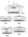
- FIG. 1A typical known baffle 2 is shown in Fig. 1 . It comprises a front wall 20 running parallel to the substrate portions 5, 8 and side walls 22, 24 running perpendicular thereto.
- the baffle 2encloses the module in the way of a housing.
- a typical thickness t of the front wallis 100-300 ⁇ m.
- the baffle 2is typically made of plastic, e.g. in an injection molding process.
- the front wall 20 of the baffle 2has a through-hole 26 with typically circular cross section which serves as an entry aperture for light.
- the viewing angle or field of view of the image capturing element 9is defined by the distance of the through-hole 26 to the image capturing element 9, as well as the diameter of the through-hole 26.
- the side wall 26a of the through-hole 26is tapered and defines a cone with an opening angle ⁇ .
- the front wall 20 with a thickness t of several 100 ⁇ mhas the effect that light incident on the device or the front wall 20 under small angles of incidence ⁇ is prevented from entering the camera device 1 via the through-hole 26 (for an infinitesimal small thickness t, also light impinging under ⁇ ⁇ 0° would enter the module).
- the baffle 2defines a collection angle ⁇ collect for incident light. It is desired that ⁇ collect is smaller than 90°, because rays entering under a very small angle of incidence generally correspond to stray light and/or lead to reflections/straying within the module.
- the non-infinitesimally small thickness t of the front wall 20leads to artifacts in the image generated by the image capturing element 9.
- Fig. 1there can be reflections/straying at the side wall 26a of the through hole 26.
- Such a reflected ray 28is schematically shown in bold dashed lines.
- top lens element 3is freely accessible through the through-hole 26. It can thus be contaminated or damaged during manufacture of the device or during use.
- Fig. 2shows a baffle 30.
- the baffle 30comprises a generally transparent baffle substrate portion 32, e.g. a portion of a glass wafer or any other generally planar piece of material, which is generally transparent in the optical range.
- the baffle substrate portion 32has a generally planar front surface 33 and a generally planar rear surface 34, i.e. without a cut-out like the prior art through hole 26.
- the substrate portion 32has a thickness t', e.g. in the range of 150-500 ⁇ m.
- t'e.g. in the range of 150-500 ⁇ m.
- the baffle substrate portioncould also be pre-shaped with, for example, integrated spacers.
- the layers 35, 36cover the whole area of the respective surface 33, 34 with the exception of a first and second opening 37, 38 in a middle region thereof.
- the openings 37, 38preferably have the shape of circles with diameters d1 and d2. They could have other shapes as well.
- the openings 37, 38are arranged concentrically with respect to one another, as seen in an axial direction.
- the center of the openings 37, 38preferably, but not necessarily corresponds to the optical axis of the completed module (as shown in Fig. 3 ).
- the diameter d1 of the first opening 37is greater than the diameter d2 of the second opening 38. Both diameters range from 0,5 to 1 mm, for example.
- This arrangement of the two spaced apart layers 35, 36 with their respective openings 37, 38has generally the same effect as the baffle 2 of the prior art with its through-hole 26.
- the openings 37, 38define the angles ⁇ and ⁇ collect as described above and thus enable definition of the field of view as well as suppression of light incident under small incidence angles. Light can enter the module via the openings 37, 38 and the transparent material of the baffle substrate portion 32.
- FIG. 2A ray 28 corresponding to an incidence on the side wall 26a in Fig. 1 . is shown in bold dashed lines. This ray 28 is not reflected, because there are no physical side walls. Instead, it enters the baffle substrate portion 32 and is reflected at the interface to the first and second layers 35, 36. Consequently, the light cannot pass the baffle 30.
- baffle 30can act as cover window for the optical module because of the continuous, but in parts transparent baffle substrate.
- the baffle 30has, by means of the two layers 35, 36 on both sides of a transparent substrate and the openings therein, an optically transparent, but mechanically impermeable window which has advanced performance compared to prior art baffles.
- a lens element 3is arranged on the rear surface 34 of the baffle substrate portion 32 in the region of the second opening 38.
- the lens elementcorresponds to the top lens element 3 in Fig. 1 . It covers the complete area of the second opening 38, and is even wider, such that all light passing through the opening 38 is affected by the lens element 3.
- the second layeris, at least in the bordering regions of the opening 28, sandwiched between the material of the lens element 3 and the baffle substrate portion 32.
- the lens 3could also be laterally smaller than the opening 38.
- Fig. 3-7show camera devices 1 with a baffle 30 as shown in Fig. 2 .
- These embodimentshave the advantage that the baffle substrate portion 30 is used to support the lens needed to image an object onto the image capturing element. This is not possible with prior art devices. It can thus be done without a separate lens substrate or lens substrate portion, and the camera device can have a smaller extent in axial direction.
- Fig. 3shows a stack comprising the baffle 30 (acting as top lens substrate 5) as shown in Fig. 2 , a further substrate portion 13 and two layers of spacers 10, 11 stacked in axial direction z and connected to one another to form an optical module 40.
- a camera device 1is formed by connecting a base substrate portion 8 (or a complete base substrate prior to dicing) with an image capturing element 9 to the stack.
- the further substrate portion 5comprises one lens elements 4 attached to is front surface.
- the top lens element 3 on the baffle substrate portion 32 and the upper lens element 4 on the further substrate portion 5correspond to the two halves of the conventional lens 3, 4 in Fig. 1 .
- the "reverse" arrangement of the lens elements with respect to Fig. 1is illustrated.
- the upper spacers 11 between the further substrate portion 13 and the baffle 30serve for keeping the lens elements 3, 4 at an axial distance from one another.
- the lower spacers 10 between the top lens substrate portion 5 and the base substrate portion 8serve for keeping the further substrate portion 13 at an axial distance from the front surface of the base substrate portion 8.
- the baffle 30limits the field of view of the image capturing element 9, reduces artifacts caused by rays incident through the first opening 37 in between the two layers 35, 36 and, as an additional effect, also serves as cover glass to protect the inside of the camera device 1 or the device 40, in particular the top lens element 3 from damage and contamination.
- Fig. 4shows a further example of the invention.
- the camera device 1comprises a baffle with a baffle substrate portion 32 as shown in Fig. 2 , a base substrate portion 8 with an image capturing clement 9 and spacers 10 between these two substrate portions 32, 8.
- the top lens element 3is directly attached to the rear surface 34 of the baffle substrate portion 32.
- the top lens element 3covers partly or completely the second opening 38 in the second layer 36. It may be replicated directly on the baffle substrate, or otherwise attached thereto.
- Fig. 5shows an unclaimed variant of the embodiment of Fig. 4 , where the top lens element 3 is arranged on the front surface 33 of the baffle substrate portion 30, where it covers the first opening 37.
- Fig. 6shows a further embodiment of the invention.
- the camera device 1comprise a baffle substrate portion 32 with the top lens 3 attached to its rear surface and a base substrate portion 8 with an image capturing element 9. It further comprises a further substrate portion 13 arranged between the baffle substrate portion 32 and the base substrate portion 8 and spaced with two layers of spacers 10, 11 therefrom.
- the further substrate portion 13comprises two lens elements 4, 4' on both of its surfaces.
- Fig. 7corresponds to an unclaimed combination of the embodiment of Fig. 4 and 5 : Lens elements 3, 4 arc arranged on both surfaces 33, 34 of the baffle substrate portion 30.
- Fig. 8a-dshows different steps of the process of manufacturing an optical module or camera device according to the invention on a wafer scale, e.g. a module as shown in Fig. 4 .
- an optically transparent substrate 320is provided and coated on both main surfaces in order to produce a thin, optically non-transparent layer 35, 36.
- the coating materialis preferably a mix of Chromium and Chromiumoxide, applied in a PVD process and having a total thickness in the range of some 100 nm (e.g. 500 nm), i.e. a few atom layers. This is generally sufficient to produce an optically dense structure that absorbs incoming light.
- the coatingcould as well be any other absorbing material, applied in a PVD, CVD, sputtering or other process.
- the coatingcould also be a thin plastic film or foil.
- first openings 37are produced in the first layer 35, and second openings 38 in the second layer 36.
- a photolithographic techniqueis used to form the openings 37, 38: A light-sensitive photoresist is applied to the respective layer and optically illuminated with a mask. A series of chemical treatments then engraves the exposure pattern into the material underneath the photoresist.
- the openings 37, 38can be produced at the same time as the layers 35, 36 by leaving certain areas blank. This could be achieved by covering these areas with a material to which the material of the layers 35, 36 does not adhere, such that it can be washed off.
- lens elements 3are formed on the rear surface of the baffle substrate 320 in the regions of the second openings 38. They are preferably formed by means of a replication technique on wafer scale. For example, a replication tool having replication sections with a surface structure corresponding to the negative of the shape of the lens elements 3 is provided, and then aligned and brought into contact with the substrate 320 with a replication material between the replication sections and the rear surface of the substrate 320. The replication material is then hardened.
- lens elementscould also be formed on an intermediate substrate ( Fig. 3 or Fig. 6 ).
- An additional substrate 50which could be a substrate carrying a plurality of lens elements or a base substrate carrying a plurality of image capturing elements, is aligned with and brought into contact with the substrate 320.
- the spacers and substratesare then connected, e.g. by means of a UV-curable adhesive, in order to form a wafer stack 100 (wafer scale package).
- Such a completed stack 100is shown in Fig. 7d .
- Individual optical modules 40, or, in case of a base substrate with image capturing elements as additional substrate 50, camera devices 1are formed by dicing the stack 100 along planes P running in axial direction, preferably through the spacers 10.
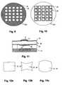
- Fig. 9 and 10show plan views of the baffle substrate 320, here by way of example of the rear surface.
- the substrate 320comprises a circular plate.
- An optically intransparent layer 36is formed thereon, here on the rear surface of the substrate 320.
- Openings 38arc formed in the layer by means of removing deposited material or by selectively depositing material only in the areas around the openings 38.
- the layer 36is formed only in regions around the openings 38, while leaving other areas uncovered. These free areas have improved surface properties, e.g. for bonding the spacer substrate to the baffle substrate by means of an UV curable adhesive.
- Fig. 11show an unclaimed embodiment where the first openings 37 in the first layer 35 on the front surface 33 are smaller than the second openings 38 in the second layer 36 on the rear surface 34. The effect is generally the same as illustrated in Fig. 2 .
- Lens elements 3, 4may be present on one or both surfaces 33, 34.
- Fig. 12a-cshow examples for non-circular shapes of the first and second openings 37, 38.
- Fig. 12ashows a rectangular opening 37, 38.
- Fig. 12bshows a cushion shape, and
- Fig. 12ca barrel shape.
- the contour of the openingpreferably corresponds to the image of the active area of the sensor in the plane of the opening, as generated by the lens elements.
- the spot of light passing through the openinghas thus the shape of the sensor, the sensor is illuminated homogeneously, and scattered light is reduced.
- Baffles with the described non-circular shapescan also be used in connection with other optical modules or camera devices, e.g. as shown in the other figures.
- conventional bafflesreal holes in a substrate that has a certain thickness in direction of the optical axis
- the contourpreferably has 2-fold or 4-fold symmetry. Rectangular, cushion-like or barrel-like shapes are preferred in connection with rectangular sensors.
- Fig. 13a-cshow that the invention is not limited to the case where a baffle is defined by two intransparent layers, wherein Fig. 13 shows an unclaimed embodiment.
- the three-dimensional passage for lightcan as well be defined by three or more layers 35, 36, 36', 36" with corresponding openings therein.
- the openingsmay 5 have an arbitrary shape, e.g. circular or like in Figs. 12a-c .
- the shapesare not necessarily the same.
- the diameterscan increase or decrease in direction of light propagation, or can first decrease, then increase or vice versa.
- lens elementsare arranged also between the first and last layer, as seen in direction of light propagation.
- the camera device of Fig. 13ahas two substrates or substrate portions. It generally corresponds to the embodiment of Fig. 6 with the exception that there arc three non-transparent layers 35, 36, 36', arranged on the top and rear surface of the first substrate and on the top surface of the second substrate.
- the device of Fig. 13bcorresponds to Fig. 13a , but has four non-transparent layers 15 35, 36, 36', 36" arranged on both surfaces of the two substrate portions.
- Fig. 13cthere are three non-transparent layers 35, 36, 36', 36", arranged on the surfaces of the two substrates, with the exception of the top surface of the first substrate.
- Figs 13a-cshow the versatility of the invention and the ability to create almost any shape of the three dimensional passage. There could be 20 even more substrates with corresponding non-transparent layers and with or without lens elements.
Landscapes
- Physics & Mathematics (AREA)
- Optics & Photonics (AREA)
- General Physics & Mathematics (AREA)
- Engineering & Computer Science (AREA)
- Multimedia (AREA)
- Signal Processing (AREA)
- Health & Medical Sciences (AREA)
- Mechanical Engineering (AREA)
- Ophthalmology & Optometry (AREA)
- Manufacturing & Machinery (AREA)
- Studio Devices (AREA)
- Transforming Light Signals Into Electric Signals (AREA)
- Solid State Image Pick-Up Elements (AREA)
- Optical Elements Other Than Lenses (AREA)
Description
- The invention is in the field of integrated optical modules, in particular integrated camera devices with an image capturing element, such as a CCD sensor, and at least one lens element for imaging an object on the image capturing element, e.g. a refractive and/or diffractive lens. Integrated device means that all components are arranged in a well defined spatial relationship. Such integrated camera devices are, for example, cameras of mobile phones which are preferably manufactured in a mass production process at low cost.
- More concretely, the invention relates to a camera device comprising a baffle that defines a predetermined field of view (FOV) of the image capturing element, while suppressing beam paths coming from points outside this FOV. The invention further relates to methods for manufacturing a. plurality of camera devices.
- Especially in the field of mobile phones with cameras, but also for other applications, it is desirable to have a camera device that can be mass produced at low cost in an as simple process as possible and still has a good image quality. Such camera devices comprise an image capturing element and at least one lens element arranged along a common axis and are known from
WO 2004/027880 , for example. The known camera devices are manufactured on a wafer scale by replicating a plurality of lens elements on a disk-like substrate (wafer), stacking and connecting the substrates to form a wafer scale package (wafer stack) and dicing the stack in order to separate the individual camera devices from one another. - The camera devices are integrated optical modules, which include functional elements such as the image capturing element and the at least one lens stacked together along the general direction of light propagation. These elements are arranged in a predetermined spatial relationship with respect to one another (integrated device) such that further alignment with each other is not needed, leaving only the integrated device as such to be aligned with other systems.
- Wafer-scale replication of lens elements allows the fabrication of several hundreds of generally identical devices with a single step, e.g. a single or double-sided UV-embossing process. Replication techniques include injection molding, roller hot embossing, flat-bed hot embossing, UV embossing. As an example, in the UV embossing process the surface topology of a master structure is replicated into a thin film of a UV-curable replication material such as an UV curable epoxy resin on top of a substrate. The replicated surface topology can be a refractive or a diffractive optically effective structure, or a combination of both. For replicating, a replication tool bearing a plurality of replication sections that are a negative copy of the optical structures to be manufactured is prepared, e.g. from a master. The tool is then used to UV-emboss the epoxy resin. The master can be a lithographically fabricated structure in fused silica or silicon, a laser or e-beam written structure, a diamond turned structure or any other type of structure. The master may also be a submaster produced in a multi stage generation process by replication from a (super) master.
- A substrate or wafer in the meaning used in this text is a disc or a rectangular plate or a plate of any other shape of any dimensionally stable, often transparent material. The diameter of a wafer disk is typically between 5 cm and 40 cm, for example between 10 cm and 31 cm. Often it is cylindrical with a diameter of either 2, 4, 6, 8 or 12 inches, one inch being about 2,54 cm. The wafer thickness is for example between 0,2 mm and 10 mm, typically between 0,4 mm and 6 mm.
- If light needs to travel through the substrate, the substrate is at least partially transparent. Preferably, especially if CMOS sensors are present, at least one of the optical surfaces comprises a coating acting as IR cutoff filter. Otherwise, the substrate can be nontransparent as well. In case of a camera device, at least one substrate bears electro-optical components, like the image capturing element, and may thus be a silicon or GaAs or other semiconductor based wafer; it may also be a CMOS wafer or a wafer carrying CCD arrays or an array of Position Sensitive Detectors.
- Such integrated optical modules can be manufactured by stacking wafers along the axis corresponding to the direction of the smallest wafer dimension (axial direction). The wafers comprise functional elements, like lens elements or image capturing elements, in a well defined spatial arrangement on the wafer. By choosing this spatial arrangement in an adequate way, a wafer stack comprising a plurality of generally identical integrated optical modules can be formed, wherein the elements of the optical module have a well defined spatial relationship with respect to one another.
- By spacers, e.g. a plurality of separated spacers or an interconnected spacer matrix as disclosed in
US 2003/0010431 orWO 2004/027880 , the wafers can be spaced from one another, and lens elements can also be arranged between the wafers on a wafer surface facing another wafer. - It is known to place a baffle in front of the top lens element of a camera device. A baffle is an element that defines a three-dimensional passage for light but is otherwise intransparent for light. In a camera device, a baffle serves to define a field of view (FOV) of the image capturing element and to suppress beam paths coming from points outside this FOV. Known baffles consist of a layer of non-transparent material having a given thickness in axial direction and a through-hole for light transmission with normally varying cross sectional areas. In known baffles, the through-hole has the shape of a truncated cone with a given extent in axial direction and given opening angle. The thickness as well as the angle of the side walls of the through hole determines the FOV and the critical angle (collection angle) under which incident light can pass the baffle and enter the camera device. It is often desired that the collection angle does not exceed a predetermined value. This is because light entering the device under higher angles is stray light and/or may not directly fall onto the photosensitive part of the image capturing element but may hit the photosensitive part only after one or more reflections inside the camera device. This may lead to artifacts in the image generated by the image capturing element, and thus to a reduced image quality.
- Known baffles have thus a thickness of several 100 µm (e.g. 100-300 µm) and side walls of the through hole which are tapered with respect to the normal direction of the front wall baffle such that an opening with a varying cross section having a diameter in the range of 1-3 mm is formed. This, among other parameters of the sensor and optical system, restricts the full angle of the field of view to about 40 to 80°. A disadvantage of such baffles are reflections at the side walls of the through hole which also lead to artifacts in the image generated by the image capturing element, and thus to a reduced image quality. Reduction of the area of the side walls, however, is not possible, because this would lead to an increased collection of unwanted stray light.
- Known baffles are normally injection molded parts. They are attached to the integrated camera device only after its complete manufacture, i.e. after the dicing step if a wafer scale manufacturing process is employed. This is not compatible with low cost wafer scale manufacture of the optical modules. The additional steps of attaching each individual baffle to each individual camera device associated therewith is time-consuming and complicated and thus another disadvantage of known modules and manufacturing processes.
- A further disadvantage is that the optical system, or at least the top lens element, is fully accessible via the through hole. This may lead to damage and contamination.
WO 2005/041561 discloses a camera module and manufacturing method thereof, where a semiconductor housing comprises a solid-state image sensor and a lens element located above the solid-state sensor. The housing forms a shield against laterally scattered radiation, by having at least one plate of transparent material of which two sides are covered with a radiation-opaque layer which is provided with an aperture. The aperture in the layer close to the sensor has a smaller surface than the aperture in the layer located remote from the sensor. The lens element is formed in a transparent substrate which is sandwiched in between the image sensor and the plate with the apertures. This construction has the disadvantage that the number of optical interfaces (e.g. air/glass) is increased, leading to losses due to reflections at these faces.- It is an object of the invention to provide a camera device with improved image quality.
- It is a further object of the invention to provide a camera device that can be manufactured in a mass production process at low cost, and a corresponding manufacturing process.
- These objects are achieved by a camera device having the features of
claim 1 and a method for manufacturing a plurality of camera devices having the features ofclaim 8. Preferred embodiments are described in the dependent claims and the description and are shown in the drawings. - The optical module for the camera device comprises a top lens element and optionally further lens elements for imaging an object on the image capturing element. It further comprises a baffle which defines a field of view of the image capturing element in the assembled camera device by geometrically determining a critical angle under which incident light can enter the camera device and eventually fall onto a photosensitive part of the image capturing element. An image capturing element arranged on a base substrate portion is present in the completed camera device. According to the invention, the baffle comprises a generally transparent baffle substrate portion having a front surface and a rear surface. It further comprises a generally optically non-transparent first layer on the front surface which has a first opening in an inner region of the front surface, and a generally optically non-transparent second layer on the rear surface which has a second opening in an inner region of the rear surface. This generally corresponds to two planar apertures that are arranged at a distance from one another, as seen in a direction normal to their planes, with the transparent substrate sandwiched in between the layers. The layers can be very thin (e.g. several hundred nm or few atom layers), because it only needs to have a thickness sufficient to achieve an optical density that is sufficient to completely or at least partially block light transmission through the layer. Light can then reach the image capturing element only by passing through the first opening and subsequently through the second opening. Among other parameters, the field of view is determined by the shape of the two openings, their axial distance and their lateral position with respect to one another.
- The first and second openings are arranged at an axial distance from one another, said distance being defined by the thickness of the baffle substrate. This distance may correspond to the thickness of the non-transparent layer in conventional baffles, but may also be smaller. The shape of the openings may, for example, be circular, wherein the circles are preferably concentric. Preferably, the first opening has a larger diameter than the second opening.
- The top lens element is arranged on the front or rear surface of the baffle substrate in the region of the first or second opening in the non-transparent layer.
- In combination, the spaced apart first and second openings with the lens element directly attached to the baffle substrate portion form a passage for light that has generally the same effect as a conventional baffle with a through-hole and a lens spaced therefrom, but the following advantages:
- Though the double layers with first and second openings have the same effect as a through hole with spaced front and rear surface, there are no physical side walls present. Consequently, there are no artifacts caused by reflection at such side walls. Light enters the camera device either without reflections, or not at all. Light rays that would hit the side walls of the through-hole in a conventional baffle here enter the transparent baffle substrate portion. They are trapped by total internal reflection and consequently suppressed.
- As there is no through-hole, all lens elements arranged inside the camera device are fully protected from damage or contamination. In particular, the baffle substrate ensures scratch protection of the top lens, as it is arranged on the rear surface. It can also ensure protection of further optical elements, including lens elements and the image capturing element, from contamination and damage during the dicing step in a wafer scale manufacturing process.
- The baffles can be manufactured on a wafer scale, e.g. by coating a transparent substrate (wafer) such that non-transparent layers are formed on both main surfaces, and by removing the coating in predetermined regions in order to form a plurality of first and second openings. This makes the attachment of the baffles fully compatible with a wafer scale manufacturing process of the camera device as such (without the baffle). It can be done without attaching individual baffles to individual integrated devices, and thus in a much more efficient way and at reduced cost.
- Forming the through-hole in conventional baffles is mechanically complicated. According to the invention, no through-hole is needed. The openings in the first and second layers, which are much thinner than the conventional baffle, can be formed by known techniques, e.g. by photolithography, on a wafer scale. Thus, manufacture of the baffle as such is easier.
- The baffle substrate serves as a substrate for the top lens. The top lens is arranged on the rear surface in close proximity of the second opening. As a consequence, the baffle substrate has a double function, and it can be done without a separate carrier substrate for the top lens. The whole module can thus be made thinner and with less components. Furthermore, the number of material interfaces (air-glass, air-plastic) within the module is reduced. Efforts for special treatment of the surfaces or other corrections in order to reduce reflections and to improve image quality can thus be reduced. If, as in a preferred embodiment, the front surface of the baffle substrate portion, is planar (with exception of the layer), all lens elements present are arranged in the interior of the module and thus protected from contamination and damage.
- The baffle can be manufactured by applying one or more non-transparent layers to one or more transparent substrates. This has the advantage that arbitrary shapes of the opening and of the three dimensional passage for light can be realized. The shape of the opening can for example be adapted to the shape of the active sensor area to achieve a more homogenous light distribution on the sensor. For rectangular sensors it is advantageous to use openings that have a generally rectangular base wherein the side lines are curved in a concave or convex manner (cushion shape, barrel shape). Any surface of any substrate may serve as carrier for a non-transparent layer, and also more than two layers, e.g. three or four, may be present with arbitrary shapes of the respective opening.
- The top lens element is a convex semi-lens, wherein the lens is arched towards the image capturing element. It should be noted that, in conventional designs, the top lens element is always placed on top of a substrate, thus being arched towards the object to be imaged. According to the invention, the top lens element of the invention is "reversed" with respect to such known designs. The invention enables a design where two lens elements are arranged on different substrates and face one another. Regarding the optical function, this generally corresponds to a classical double-sided lens or two lens elements on a common substrate. The "reverse" design, however, provides additional freedom of design, as parameters like the distance of the two curved surfaces is not limited by the thickness of the substrate but can be freely chosen.
- As the front surface of the baffle substrate portion is preferably planar, the baffle substrate can, over its entire area, rest against a support during replication of the top lens elements on its rear surface. The baffle substrates thus does not need to have the stability required for replication by itself; it can be made thinner than conventional substrates.
- The present description also describes a wafer scale package, comprising a baffle substrate a plurality of a top lens elements, optionally a base substrate with a plurality of image capturing elements, and optionally further lens elements for imaging an object on the image capturing elements. The generally transparent baffle substrate has a generally planar front surface and a generally planar rear surface, a generally non-transparent first layer with a plurality of second openings on the front surface and a generally non-transparent second layer with a plurality of second openings on the rear surface, wherein the first and second openings are shaped to define, among other parameters, a predetermined field of view of the image capturing element. The top lens elements arc arranged on the front or rear surface of the baffle substrate. In addition to the advantages of the optical module or the camera device itself, the package has the advantage that individual devices/camera devices already comprising baffles can be manufactured in a mass production process from said wafer scale package by means of dicing.
- The camera device as well as the package may also contain a spacer or a spacer layer, e.g. a spacer wafer or spacer plate with a plurality of openings or a plurality of individual spacers. The spacer or spacer layer ensures a well defined distance between the substrates and consequently between the baffle, the lens elements and the image capturing element. In a preferred embodiment, the lens elements are fully encapsulated by the substrates and the spacers, and are thus well protected.
- The invention further relates to a method for manufacturing a plurality of camera devices on a wafer scale, comprising the following steps:
- 1. Providing a generally transparent baffle substrate having a front surface and a rear surface, a generally non-transparent first layer with a plurality of first openings on the front surface and a generally non-transparent second layer with a plurality of second openings on the rear surface, and with a plurality of lens elements on the front or rear surface. The baffle substrate may be a glass wafer, or consist of any other transparent material. The non-transparent layers may be constituted by a thin film on the respective surfaces, e.g. formed by applying a non-transparent foil or a coating of suitable material and with suitable thickness (e.g. by PVC, sputtering, CVD, painting, spraying, immersing or other processes).
- 2. Optionally, also spacer layers and/or further lens elements arranged on further (intermediate) substrates are provided.
- 3. The substrates are then stacked and connected to one another in such a way that the top lens elements, and the first and second openings and optionally also the spacers and/or further lens elements are arranged in a predetermined spatial relationship. Usually, this step includes alignment of the elements present on the different substrates along common axes.
- 4. The package is then diced along predetermined planes, in order to separate the individual modules from one another.
Optionally, in case of wafer scale production of complete camera devices: - 5. Providing a base substrate having a plurality of image capturing elements prior to or after dicing. The base substrate may be a silicon or GaAs or other semiconductor based wafer; it may also be a CMOS wafer or a wafer carrying CCD arrays or an array of Position Sensitive Detectors.
- Preferably, the top lens elements are formed on the baffle substrate by means of a replication process. Preferably, at first the first and second layers are formed by depositing a material on the surfaces. Then, openings are formed by selectively removing this material in certain regions, e.g. by photolithography and etching. Then, the top lens elements are replicated in the regions of the openings, preferably covering a slightly larger area than the second openings. The openings could also be formed by depositing material on selected regions of the front and rear surface, e.g. by protecting certain areas with a shield or an anti-adhesion coating.
- The baffle substrate with the lens elements could also be manufactured in one piece, e.g. by injection molding or another replication process.
- The present description also describes a baffle substrate with a plurality of baffles, and to a corresponding manufacturing method. The baffle substrate comprises a generally transparent substrate having a front surface and a rear surface, a generally non-transparent first layer with a plurality of second openings on the front surface and a generally non-transparent second layer with a plurality of second openings on the rear surface, as well as a plurality of lens elements attached to the front or rear surface. It is manufactured by providing a generally transparent substrate having a front surface and a rear surface, e.g. a glass wafer; providing the front surface with a generally non-transparent first layer and providing the rear surface with a generally non-transparent second layer, e.g. by applying a thin film or coating, for example by means of PVD, sputtering, CVD or other material depositing processes; and providing the first layer with a plurality of first openings and providing the first layer with a plurality of second openings, preferably by photolithography.
- One preferred application of the camera device is for CMOS cameras, including CMOS cameras for mobile phones. Here, the front surface of the baffle substrate, which can be flat and unstructured with the exception of the (thin) first layer, could be directly used as the cover window of the camera, of a module within the camera, or even of the phone cover instead of a separate cover window. This leads to both simplified assembly and lower material cost.
- Among others, the invention has the advantages that the number of optical interfaces and losses in connection therewith can be reduced, smaller axial dimensions of the device can be achieved, unwanted light can be suppressed more efficiently, protection of functional elements of the module is ensured during manufacture and use, and the production process of the baffles as well as of the complete devices is fully compatible with a wafer scale manufacture, and can thus be realized in a mass production process at low costs.
Fig. 1 shows schematically a camera device according to the prior art;Fig. 2 show schematically a baffle according to the invention;Fig. 3, 4, 6 schematically camera devices according to the invention;Fig. 5, 7 show schematically unclaimed camera devices;Fig. 8a-d show schematically details of the manufacturing process;Fig. 9, 10 show baffle substrates;Fig. 11 shows an unclaimed camera device wherein the first openings as smaller than the second openings;Fig. 12a-c show examples for the shape of the first and second openings;Fig. 13a-c show further examples for camera devices with three or four non-transparent layers.- The
camera device 1 according to the prior art comprises an optical system with one bi-convex lens, which is here constituted by two half-lenses rear surface 7 of alens substrate portion 5. Thelens elements camera device 1 further comprises abase substrate portion 8 with animage capturing element 9, e.g. a CMOS substrate with an image sensor. Thelens substrate portion 5 and thebase substrate portion 8 are stacked in an axial direction z (normal to their main surfaces) and are spaced from one another by means ofspacers 10. Thereby, well defined axial distance between thelens elements image capturing element 9 is realized. The modules consisting of thelens substrate portion 5, spacers andbase substrate portion 8 are typically manufactured on wafer scale by means of providing a lens substrate having a plurality oflens elements image capturing element 9; then stacking and connecting these substrates, and subsequent dicing. - According to the prior art, these individual modules are provided with a
baffle 2 only after the dicing step. A typical knownbaffle 2 is shown inFig. 1 . It comprises afront wall 20 running parallel to thesubstrate portions baffle 2 encloses the module in the way of a housing. A typical thickness t of the front wall is 100-300 µm. Thebaffle 2 is typically made of plastic, e.g. in an injection molding process. - The
front wall 20 of thebaffle 2 has a through-hole 26 with typically circular cross section which serves as an entry aperture for light. The viewing angle or field of view of theimage capturing element 9 is defined by the distance of the through-hole 26 to theimage capturing element 9, as well as the diameter of the through-hole 26. The side wall 26a of the through-hole 26 is tapered and defines a cone with an opening angle Ω. Thefront wall 20 with a thickness t of several 100 µm has the effect that light incident on the device or thefront wall 20 under small angles of incidence α is prevented from entering thecamera device 1 via the through-hole 26 (for an infinitesimal small thickness t, also light impinging under α ≈0° would enter the module). Consequently, thebaffle 2 defines a collection angle θcollect for incident light. It is desired that θcollect is smaller than 90°, because rays entering under a very small angle of incidence generally correspond to stray light and/or lead to reflections/straying within the module. - On the other hand, the non-infinitesimally small thickness t of the
front wall 20 leads to artifacts in the image generated by theimage capturing element 9. As shown inFig. 1 , there can be reflections/straying at the side wall 26a of the throughhole 26. Such a reflectedray 28 is schematically shown in bold dashed lines. These reflections are an intrinsic problem of the prior art baffles. - Another problem is that the
top lens element 3 is freely accessible through the through-hole 26. It can thus be contaminated or damaged during manufacture of the device or during use. Fig. 2 shows abaffle 30. Thebaffle 30 comprises a generally transparentbaffle substrate portion 32, e.g. a portion of a glass wafer or any other generally planar piece of material, which is generally transparent in the optical range.- In this embodiment, the
baffle substrate portion 32 has a generally planarfront surface 33 and a generally planarrear surface 34, i.e. without a cut-out like the prior art throughhole 26. Thesubstrate portion 32 has a thickness t', e.g. in the range of 150-500 µm. As shown inFig. 4 or 6 , there could be a lens element attached to therear surface 34. The baffle substrate portion could also be pre-shaped with, for example, integrated spacers. - There is a
first layer 35 of generally non-transparent material on thefront surface 33 and asecond layer 36 of generally non-transparent material on therear surface 34. Thelayers respective surface second opening openings openings openings Fig. 3 ). The diameter d1 of thefirst opening 37 is greater than the diameter d2 of thesecond opening 38. Both diameters range from 0,5 to 1 mm, for example. - This arrangement of the two spaced apart layers 35, 36 with their
respective openings baffle 2 of the prior art with its through-hole 26. In particular, theopenings openings baffle substrate portion 32. - The advantage of the invention is also illustrated in
Fig. 2 : Aray 28 corresponding to an incidence on the side wall 26a inFig. 1 . is shown in bold dashed lines. Thisray 28 is not reflected, because there are no physical side walls. Instead, it enters thebaffle substrate portion 32 and is reflected at the interface to the first andsecond layers baffle 30. - Another advantage is that the
baffle 30 can act as cover window for the optical module because of the continuous, but in parts transparent baffle substrate. - The
baffle 30 has, by means of the twolayers - A
lens element 3 is arranged on therear surface 34 of thebaffle substrate portion 32 in the region of thesecond opening 38. The lens element corresponds to thetop lens element 3 inFig. 1 . It covers the complete area of thesecond opening 38, and is even wider, such that all light passing through theopening 38 is affected by thelens element 3. The second layer is, at least in the bordering regions of theopening 28, sandwiched between the material of thelens element 3 and thebaffle substrate portion 32. Thelens 3 could also be laterally smaller than theopening 38. Fig. 3-7 show camera devices 1 with abaffle 30 as shown inFig. 2 . These embodiments have the advantage that thebaffle substrate portion 30 is used to support the lens needed to image an object onto the image capturing element. This is not possible with prior art devices. It can thus be done without a separate lens substrate or lens substrate portion, and the camera device can have a smaller extent in axial direction.Fig. 3 shows a stack comprising the baffle 30 (acting as top lens substrate 5) as shown inFig. 2 , afurther substrate portion 13 and two layers ofspacers optical module 40. Acamera device 1 is formed by connecting a base substrate portion 8 (or a complete base substrate prior to dicing) with animage capturing element 9 to the stack. Thefurther substrate portion 5 comprises onelens elements 4 attached to is front surface. Thetop lens element 3 on thebaffle substrate portion 32 and theupper lens element 4 on thefurther substrate portion 5 correspond to the two halves of theconventional lens Fig. 1 . The "reverse" arrangement of the lens elements with respect toFig. 1 is illustrated.- The
upper spacers 11 between thefurther substrate portion 13 and thebaffle 30 serve for keeping thelens elements lower spacers 10 between the toplens substrate portion 5 and thebase substrate portion 8 serve for keeping thefurther substrate portion 13 at an axial distance from the front surface of thebase substrate portion 8. - The
baffle 30 limits the field of view of theimage capturing element 9, reduces artifacts caused by rays incident through thefirst opening 37 in between the twolayers camera device 1 or thedevice 40, in particular thetop lens element 3 from damage and contamination. Fig. 4 shows a further example of the invention. Thecamera device 1 comprises a baffle with abaffle substrate portion 32 as shown inFig. 2 , abase substrate portion 8 with animage capturing clement 9 andspacers 10 between these twosubstrate portions top lens element 3 is directly attached to therear surface 34 of thebaffle substrate portion 32. Thetop lens element 3 covers partly or completely thesecond opening 38 in thesecond layer 36. It may be replicated directly on the baffle substrate, or otherwise attached thereto.Fig. 5 shows an unclaimed variant of the embodiment ofFig. 4 , where thetop lens element 3 is arranged on thefront surface 33 of thebaffle substrate portion 30, where it covers thefirst opening 37.Fig. 6 shows a further embodiment of the invention. Thecamera device 1 comprise abaffle substrate portion 32 with thetop lens 3 attached to its rear surface and abase substrate portion 8 with animage capturing element 9. It further comprises afurther substrate portion 13 arranged between thebaffle substrate portion 32 and thebase substrate portion 8 and spaced with two layers ofspacers further substrate portion 13 comprises twolens elements 4, 4' on both of its surfaces.- It is also possible that there is more than one single or double sided intermediate substrate portion.
Fig. 7 corresponds to an unclaimed combination of the embodiment ofFig. 4 and 5 :Lens elements surfaces baffle substrate portion 30.Fig. 8a-d shows different steps of the process of manufacturing an optical module or camera device according to the invention on a wafer scale, e.g. a module as shown inFig. 4 . InFig. 8a , an opticallytransparent substrate 320 is provided and coated on both main surfaces in order to produce a thin, opticallynon-transparent layer - In the next step, which is shown in
Fig. 8b ,first openings 37 are produced in thefirst layer 35, andsecond openings 38 in thesecond layer 36. Preferably, a photolithographic technique is used to form theopenings 37, 38: A light-sensitive photoresist is applied to the respective layer and optically illuminated with a mask. A series of chemical treatments then engraves the exposure pattern into the material underneath the photoresist. - As an alternative, the
openings layers layers - In the next step, which is shown in
Fig. 8c ,lens elements 3 are formed on the rear surface of thebaffle substrate 320 in the regions of thesecond openings 38. They are preferably formed by means of a replication technique on wafer scale. For example, a replication tool having replication sections with a surface structure corresponding to the negative of the shape of thelens elements 3 is provided, and then aligned and brought into contact with thesubstrate 320 with a replication material between the replication sections and the rear surface of thesubstrate 320. The replication material is then hardened. - In addition, further lens elements could also be formed on an intermediate substrate (
Fig. 3 or Fig. 6 ). - An
additional substrate 50, which could be a substrate carrying a plurality of lens elements or a base substrate carrying a plurality of image capturing elements, is aligned with and brought into contact with thesubstrate 320. A layer ofspacers 10, e.g. a spacer matrix, is arranged in between thesubstrates - Such a completed
stack 100 is shown inFig. 7d . Individualoptical modules 40, or, in case of a base substrate with image capturing elements asadditional substrate 50,camera devices 1 are formed by dicing thestack 100 along planes P running in axial direction, preferably through thespacers 10. Fig. 9 and 10 show plan views of thebaffle substrate 320, here by way of example of the rear surface. Thesubstrate 320 comprises a circular plate. An opticallyintransparent layer 36 is formed thereon, here on the rear surface of thesubstrate 320.Openings 38 arc formed in the layer by means of removing deposited material or by selectively depositing material only in the areas around theopenings 38.- In
Fig. 10 , thelayer 36 is formed only in regions around theopenings 38, while leaving other areas uncovered. These free areas have improved surface properties, e.g. for bonding the spacer substrate to the baffle substrate by means of an UV curable adhesive. Fig. 11 show an unclaimed embodiment where thefirst openings 37 in thefirst layer 35 on thefront surface 33 are smaller than thesecond openings 38 in thesecond layer 36 on therear surface 34. The effect is generally the same as illustrated inFig. 2 .Lens elements surfaces Fig. 12a-c show examples for non-circular shapes of the first andsecond openings Fig. 12a shows arectangular opening Fig. 12b shows a cushion shape, andFig. 12c a barrel shape.- Generally, the contour of the opening preferably corresponds to the image of the active area of the sensor in the plane of the opening, as generated by the lens elements. The spot of light passing through the opening has thus the shape of the sensor, the sensor is illuminated homogeneously, and scattered light is reduced.
- Baffles with the described non-circular shapes can also be used in connection with other optical modules or camera devices, e.g. as shown in the other figures. In particular, also conventional baffles (real holes in a substrate that has a certain thickness in direction of the optical axis) could be shaped like that. The contour preferably has 2-fold or 4-fold symmetry. Rectangular, cushion-like or barrel-like shapes are preferred in connection with rectangular sensors.
Fig. 13a-c show that the invention is not limited to the case where a baffle is defined by two intransparent layers, whereinFig. 13 shows an unclaimed embodiment. The three-dimensional passage for light can as well be defined by three ormore layers Figs. 12a-c . The shapes are not necessarily the same. The diameters can increase or decrease in direction of light propagation, or can first decrease, then increase or vice versa. Preferably, lens elements are arranged also between the first and last layer, as seen in direction of light propagation. - 10 The camera device of
Fig. 13a has two substrates or substrate portions. It generally corresponds to the embodiment ofFig. 6 with the exception that there arc threenon-transparent layers - The device of
Fig. 13b corresponds toFig. 13a , but has four non-transparent layers 15 35, 36, 36', 36" arranged on both surfaces of the two substrate portions. - In the unclaimed embodiment of
Fig. 13c , there are threenon-transparent layers Figs 13a-c show the versatility of the invention and the ability to create almost any shape of the three dimensional passage. There could be 20 even more substrates with corresponding non-transparent layers and with or without lens elements.
Claims (10)
- A camera device comprising:- an image capturing element (9) arranged on a base substrate portion (8),- at least one lens element (3, 4) for imaging an object on the image capturing element (9),- a baffle (30) defining a predetermined field of view of the image capturing element (9), wherein the baffle (30) comprises a generally transparent baffle substrate portion. (32) having a front surface (33) facing the exterior and a rear surface (34) facing the base substrate portion (8), a generally non-transparent first layer (35) with a first opening (37) on the front surface and a generally non-transparent second layer (36) with a second opening (38) on the rear surface,
wherein at least one lens clement (3) is a convex semi-lens;
wherein an end face of the camera device is constituted by the front surface (33) of the baffle substrate portion (32);
wherein the camera device further comprises at least one spacer (11) between the baffle substrate portion (32) and the base substrate portion (8), wherein said at least one spacer (11) is not identical with said second layer (36);
wherein the front surface (37) of the baffle substrate portion (32) is planar with exception of the first layer (35);
wherein all lens elements (3, 4, 4') present are fully encapsulated by the substrate portions (8, 32) and the at least one spacer (11);
characterized in that:- the at least one lens element (3) being a convex semi-lens is arched towards the image capturing element and is arranged directly on the rear surface (36) of the baffle substrate portion (32) in the region of the opening (38) therein, wherein the baffle substrate portion (32) is a carrier substrate for this lens element (3, 4);- the second layer (36) is, at least in a bordering region of the second opening (38), arranged in between the lens element (3, 4), which is a convex semi-lens and on the baffle substrate portion (32), and the rear surface (36) of the baffle substrate portion (32). - Camera device according to claim 1, wherein the cross sectional area of the first opening (37) is larger than the cross sectional area or the second opening (38), or wherein the cross sectional area of the first opening (37) is smaller than the cross sectional area of the second opening (38).
- Camera device according to one of the preceding claims, wherein the first and second opening (37, 38) have the shape of circles, which are preferably arranged concentrically with respect to one another.
- Camera device according to one of the preceding claims, wherein the lens element (3, 4) on the baffle substrate portion (32) covers an area of the rear surface (34) that is larger than the cross sectional area of the second opening (38).
- Camera device according to one of the preceding claims, further comprising at least one generally transparent intermediate substrate portion (13) arranged between the baffle substrate portion (32) and the base substrate portion (8) and carrying at least one further lens element.
- Camera device according to one of the preceding claims, wherein the generally non-transparent first and second layers (35, 36) arc constituted by a thin film or a coating on the baffle substrate portion, preferably a coating containing chromium and/or chromium oxide, or a thin plastic foil.
- Camera device according to one of claims 1-6, wherein the contour of the first and/or second opening (37, 38) corresponds to the image of the active area of the image capturing element (9) in the plane of the opening, as generated by the at least one lens element (3, 4).
- Method for manufacturing a plurality of camera devices according to one of claims 1-6 on a wafer scale, comprising the following steps:- Providing a generally transparent baffle substrate (320) having a front surface (33) and a rear surface (34), a generally non-transparent first layer (35) with a plurality of first openings (37) on the front surface (33) and a generally non-transparent second layer (36) with a plurality of second openings (38) on the rear surface;- Directly attaching a plurality of lens elements (3, 4) to the rear surface of the baffle substrate in the regions of the second openings while leaving the front surface of the baffle substrate free of lens elements,;- providing a base substrate having a plurality of image capturing elements (8);- providing at least one spacer layer;- stacking and connecting the substrates and then spacer layer such that all lens elements (3, 4) present are fully encapsulated by the substrates and the spacer layer;- dicing the package formed in the step of stacking and connecting the substrates along predetermined planes (P).
- Method according to claim 8, wherein the step of attaching a plurality of lens elements (3, 4) comprises forming a plurality of lens elements (3, 4) on the rear surface (34) of the baffle substrate (320) by means of a replication process.
- Method according to claim 9, wherein a replication tool having replication sections with a surface structure corresponding to the negative of the shape of the lens elements (3, 4) is provided, and then aligned and brought into contact with the baffle substrate (320) with a replication material between the replication sections and the rear surface of the baffle substrate (320), while the planar front surface of the baffle substrate, over its entire area, rests against a support.
Applications Claiming Priority (2)
| Application Number | Priority Date | Filing Date | Title |
|---|---|---|---|
| US1480507P | 2007-12-19 | 2007-12-19 | |
| PCT/CH2008/000531WO2009076787A1 (en) | 2007-12-19 | 2008-12-16 | Optical module for a camera device, baffle substrate, wafer scale package, and manufacturing methods therefor |
Publications (2)
| Publication Number | Publication Date |
|---|---|
| EP2223173A1 EP2223173A1 (en) | 2010-09-01 |
| EP2223173B1true EP2223173B1 (en) | 2013-09-04 |
Family
ID=40377178
Family Applications (1)
| Application Number | Title | Priority Date | Filing Date |
|---|---|---|---|
| EP08862742.7AActiveEP2223173B1 (en) | 2007-12-19 | 2008-12-16 | Camera device and manufacturing methods therefor |
Country Status (4)
| Country | Link |
|---|---|
| US (1) | US8610823B2 (en) |
| EP (1) | EP2223173B1 (en) |
| TW (1) | TWI484237B (en) |
| WO (1) | WO2009076787A1 (en) |
Cited By (1)
| Publication number | Priority date | Publication date | Assignee | Title |
|---|---|---|---|---|
| EP4354186A1 (en)* | 2022-10-14 | 2024-04-17 | Viavi Solutions Inc. | Optical element |
Families Citing this family (82)
| Publication number | Priority date | Publication date | Assignee | Title |
|---|---|---|---|---|
| WO2010020062A1 (en) | 2008-08-20 | 2010-02-25 | Heptagon Oy | Method of manufacturing a pluralty of optical devices |
| JP5158720B2 (en)* | 2009-03-11 | 2013-03-06 | 富士フイルム株式会社 | Optical module, method for manufacturing the same, and imaging apparatus |
| CN101872033B (en)* | 2009-04-24 | 2014-04-30 | 鸿富锦精密工业(深圳)有限公司 | Shading sheet array, manufacturing method thereof and lens module array |
| US9419032B2 (en)* | 2009-08-14 | 2016-08-16 | Nanchang O-Film Optoelectronics Technology Ltd | Wafer level camera module with molded housing and method of manufacturing |
| US8351219B2 (en)* | 2009-09-03 | 2013-01-08 | Visera Technologies Company Limited | Electronic assembly for an image sensing device |
| JP2011128355A (en)* | 2009-12-17 | 2011-06-30 | Sony Corp | Imaging lens, camera module using imaging lens, manufacturing method of imaging lens, and manufacturing method of camera module |
| WO2011156928A2 (en) | 2010-06-14 | 2011-12-22 | Heptagon Oy | Camera, and method of manufacturing a plurality of cameras |
| CN103201838A (en)* | 2010-06-14 | 2013-07-10 | 赫普塔冈微光学有限公司 | Method of manufacturing a plurality of optical devices |
| JP5977745B2 (en) | 2010-08-17 | 2016-08-24 | ヘプタゴン・マイクロ・オプティクス・プライベート・リミテッドHeptagon Micro Optics Pte. Ltd. | Method for manufacturing a plurality of optical devices for a camera |
| TWI449959B (en)* | 2010-12-02 | 2014-08-21 | Himax Tech Ltd | Method of manufacturing dual-focus substrates |
| US20120154945A1 (en)* | 2010-12-16 | 2012-06-21 | William Mark Hiatt | Optical apertures and applications thereof |
| US8837060B2 (en)* | 2011-02-25 | 2014-09-16 | Visera Technologies Company Limited | Image capture lens module and wafer level packaged image capture devices |
| US20120257292A1 (en)* | 2011-04-08 | 2012-10-11 | Himax Technologies Limited | Wafer Level Lens Module and Method for Manufacturing the Wafer Level Lens Module |
| SG2014005805A (en)* | 2011-08-10 | 2014-06-27 | Heptagon Micro Optics Pte Ltd | Opto-electronic module and method for manufacturing the same |
| US10444477B2 (en) | 2011-08-25 | 2019-10-15 | Ams Sensors Singapore Pte. Ltd. | Wafer-level fabrication of optical devices with front focal length correction |
| TWI482271B (en)* | 2011-11-04 | 2015-04-21 | King Dragon Internat Inc | Image sensor package with dual substrates and the method of the same |
| US20130122247A1 (en)* | 2011-11-10 | 2013-05-16 | Omnivision Technologies, Inc. | Spacer Wafer For Wafer-Level Camera And Method For Manufacturing Same |
| TWI480961B (en)* | 2011-12-05 | 2015-04-11 | Himax Tech Ltd | Wafer-to-wafer bonding structure |
| CN104106138B (en)* | 2011-12-21 | 2017-08-15 | 新加坡恒立私人有限公司 | Optical device and optoelectronic module and method for manufacturing the optical device and optoelectronic module |
| CN103178052B (en)* | 2011-12-22 | 2015-11-18 | 奇景光电股份有限公司 | Wafer-to-Wafer Bonding Structure |
| US8804032B2 (en) | 2012-03-30 | 2014-08-12 | Omnivision Technologies, Inc. | Wafer level camera module with snap-in latch |
| US20130270426A1 (en)* | 2012-04-13 | 2013-10-17 | Global Microptics Company | Lens module |
| US8606057B1 (en) | 2012-11-02 | 2013-12-10 | Heptagon Micro Optics Pte. Ltd. | Opto-electronic modules including electrically conductive connections for integration with an electronic device |
| US9595553B2 (en)* | 2012-11-02 | 2017-03-14 | Heptagon Micro Optics Pte. Ltd. | Optical modules including focal length adjustment and fabrication of the optical modules |
| TWI565986B (en)* | 2012-11-13 | 2017-01-11 | 鴻海精密工業股份有限公司 | Optical fiber fixing device |
| EP2939053B1 (en)* | 2012-12-27 | 2019-03-20 | Heptagon Micro Optics Pte. Ltd. | Fabrication of optical elements |
| WO2014109711A1 (en) | 2013-01-10 | 2014-07-17 | Heptagon Micro Optics Pte. Ltd. | Opto-electronic modules including features to help reduce stray light and/or optical cross-talk |
| KR101634516B1 (en) | 2013-06-13 | 2016-06-28 | 코어포토닉스 리미티드 | Dual aperture zoom digital camera |
| US9857568B2 (en) | 2013-07-04 | 2018-01-02 | Corephotonics Ltd. | Miniature telephoto lens assembly |
| JP2016523389A (en) | 2013-07-04 | 2016-08-08 | コアフォトニクス リミテッド | Compact telephoto lens assembly |
| CN104347644B (en)* | 2013-07-25 | 2018-06-19 | 意法半导体研发(深圳)有限公司 | Visual detector and correlation technique with lens subassembly |
| US11036309B2 (en)* | 2013-07-31 | 2021-06-15 | Ams Sensors Singapore Pte. Ltd. | Micro-optical orientation sensor and related methods |
| US9746349B2 (en)* | 2013-09-02 | 2017-08-29 | Heptagon Micro Optics Pte. Ltd. | Opto-electronic module including a non-transparent separation member between a light emitting element and a light detecting element |
| US9880391B2 (en)* | 2013-10-01 | 2018-01-30 | Heptagon Micro Optics Pte. Ltd. | Lens array modules and wafer-level techniques for fabricating the same |
| EP3072155B1 (en)* | 2013-11-22 | 2019-05-08 | Heptagon Micro Optics Pte. Ltd. | Compact optoelectronic modules |
| CN103969714B (en)* | 2014-05-23 | 2016-08-31 | 豪威光电子科技(上海)有限公司 | Autoregistration metal-layer structure, eyeglass and preparation method thereof and eyeglass module |
| US9467606B2 (en)* | 2014-06-10 | 2016-10-11 | Omnivision Technologies, Inc. | Wafer level stepped sensor holder |
| US9392188B2 (en) | 2014-08-10 | 2016-07-12 | Corephotonics Ltd. | Zoom dual-aperture camera with folded lens |
| CN112433331B (en) | 2015-01-03 | 2022-07-08 | 核心光电有限公司 | Miniature telephoto lens module and camera using the same |
| US20160307881A1 (en)* | 2015-04-20 | 2016-10-20 | Advanced Semiconductor Engineering, Inc. | Optical sensor module and method for manufacturing the same |
| JPWO2016208403A1 (en)* | 2015-06-23 | 2018-04-12 | ソニー株式会社 | Image sensor and electronic device |
| US10901190B2 (en)* | 2015-06-23 | 2021-01-26 | The Charles Stark Draper Laboratory, Inc. | Hemispherical star camera |
| US9778443B2 (en)* | 2015-10-05 | 2017-10-03 | Omnivision Technologies, Inc. | Three-surface wide field-of-view lens system |
| WO2017069705A1 (en)* | 2015-10-22 | 2017-04-27 | Heptagon Micro Optics Pte. Ltd. | Athermal optical assembly |
| US10666841B2 (en) | 2015-11-11 | 2020-05-26 | Boston Scientific Scimed, Inc. | Visualization device and related systems and methods |
| US9915763B2 (en)* | 2015-11-13 | 2018-03-13 | Omnivision Technologies, Inc. | Stacked-lens assembly and fabrication method for same |
| US10394004B2 (en) | 2016-04-05 | 2019-08-27 | Qualcomm Incorporated | Systems and devices having single-sided wafer-level optics |
| CN109155258B (en)* | 2016-04-08 | 2022-04-26 | 赫普塔冈微光有限公司 | Thin optoelectronic modules with apertures and their fabrication |
| US10388684B2 (en) | 2016-10-04 | 2019-08-20 | Semiconductor Components Industries, Llc | Image sensor packages formed using temporary protection layers and related methods |
| KR102212611B1 (en) | 2017-02-23 | 2021-02-05 | 코어포토닉스 리미티드 | Folded camera lens designs |
| US10469718B2 (en)* | 2017-05-03 | 2019-11-05 | Omnivision Technologies, Inc. | Camera module having baffle between two glass substrates |
| US10677964B2 (en) | 2017-10-23 | 2020-06-09 | Omnivision Technologies, Inc. | Lens wafer assembly and associated method for manufacturing a stepped spacer wafer |
| EP3759538A4 (en)* | 2018-03-02 | 2021-05-05 | Corephotonics Ltd. | DESIGN OF SPACING ELEMENTS TO REDUCE PARASITIC LIGHT |
| TWI688271B (en)* | 2018-11-29 | 2020-03-11 | 香港商立景創新有限公司 | Camera device |
| CN109411549A (en)* | 2018-12-07 | 2019-03-01 | 苏州苏纳光电有限公司 | Opto chip encapsulating structure and packaging method |
| US11336830B2 (en) | 2019-01-03 | 2022-05-17 | Corephotonics Ltd. | Multi-aperture cameras with at least one two state zoom camera |
| DE102019107003A1 (en)* | 2019-03-19 | 2020-09-24 | OSRAM Opto Semiconductors Gesellschaft mit beschränkter Haftung | Cover for an optoelectronic component, optoelectronic component, use of an optoelectronic component and method for producing a cover for an optoelectronic component |
| CN113906319A (en)* | 2019-05-30 | 2022-01-07 | ams传感器新加坡私人有限公司 | Method of replicating an optical element and replicating optical element |
| WO2020256635A1 (en)* | 2019-06-19 | 2020-12-24 | Ams Sensors Singapore Pte. Ltd. | Replicating optical elements onto a substrate |
| CN113994494A (en) | 2019-07-12 | 2022-01-28 | 株式会社半导体能源研究所 | Function panel, display device, input and output device, data processing device |
| WO2021033047A1 (en) | 2019-08-21 | 2021-02-25 | Corephotonics Ltd. | Low total track length for large sensor format |
| US12072609B2 (en) | 2019-09-24 | 2024-08-27 | Corephotonics Ltd. | Slim pop-out cameras and lenses for such cameras |
| WO2021069999A1 (en) | 2019-10-11 | 2021-04-15 | 株式会社半導体エネルギー研究所 | Function panel, display device, i/o device, and information processing device |
| KR20210052936A (en) | 2019-11-01 | 2021-05-11 | 삼성전기주식회사 | Spacer and Camera Module |
| US11656538B2 (en) | 2019-11-25 | 2023-05-23 | Corephotonics Ltd. | Folded zoom camera module with adaptive aperture |
| US11689708B2 (en) | 2020-01-08 | 2023-06-27 | Corephotonics Ltd. | Multi-aperture zoom digital cameras and methods of using same |
| US11770609B2 (en) | 2020-05-30 | 2023-09-26 | Corephotonics Ltd. | Systems and methods for obtaining a super macro image |
| KR102765964B1 (en) | 2020-07-22 | 2025-02-07 | 코어포토닉스 리미티드 | Folded camera lens design |
| CN119414645A (en) | 2020-07-31 | 2025-02-11 | 核心光电有限公司 | camera |
| EP4127788A4 (en) | 2020-09-18 | 2024-06-19 | Corephotonics Ltd. | Pop-out zoom camera |
| US12271105B2 (en) | 2020-11-05 | 2025-04-08 | Corephotonics Ltd. | Scanning Tele camera based on two prism field of view scanning |
| KR20250008791A (en) | 2020-12-01 | 2025-01-15 | 코어포토닉스 리미티드 | Folded camera with continuously adaptive zoom factor |
| CN117425062A (en) | 2021-01-25 | 2024-01-19 | 核心光电有限公司 | Lens system for compact digital camera |
| WO2022200965A1 (en) | 2021-03-22 | 2022-09-29 | Corephotonics Ltd. | Folded cameras with continuously adaptive zoom factor |
| KR20240012438A (en) | 2021-06-23 | 2024-01-29 | 코어포토닉스 리미티드 | Compact folded tele camera |
| KR102685591B1 (en) | 2021-09-23 | 2024-07-15 | 코어포토닉스 리미티드 | Large aperture continuous zoom folded telecamera |
| WO2023052892A1 (en)* | 2021-09-29 | 2023-04-06 | 株式会社半導体エネルギー研究所 | Display apparatus and electronic equipment |
| CN119414565A (en) | 2021-11-02 | 2025-02-11 | 核心光电有限公司 | Camera module and mobile device |
| CN120315167A (en) | 2021-12-14 | 2025-07-15 | 核心光电有限公司 | Large aperture compact scan telephoto camera |
| TWI858467B (en)* | 2021-12-16 | 2024-10-11 | 昇佳電子股份有限公司 | Optical sensor module and packaging method thereof |
| US12348870B2 (en) | 2022-04-09 | 2025-07-01 | Corephotonics Ltd. | Spin-out 360-degree camera for smartphone |
| US12368960B2 (en) | 2022-08-05 | 2025-07-22 | Corephotonics Ltd. | Systems and methods for zoom digital camera with automatic adjustable zoom field of view |
Citations (1)
| Publication number | Priority date | Publication date | Assignee | Title |
|---|---|---|---|---|
| US20070126898A1 (en)* | 2004-09-27 | 2007-06-07 | Digital Optics Corporation | Thin camera and associated methods |
Family Cites Families (11)
| Publication number | Priority date | Publication date | Assignee | Title |
|---|---|---|---|---|
| NL7501931A (en)* | 1975-02-19 | 1976-08-23 | Philips Nv | TELEVISION ROOM WITH STAR HOUSE. |
| US5400072A (en)* | 1988-12-23 | 1995-03-21 | Hitachi, Ltd. | Video camera unit having an airtight mounting arrangement for an image sensor chip |
| JPH0927606A (en)* | 1995-07-12 | 1997-01-28 | Fuji Film Micro Device Kk | Solid-state image pick-up element of cog structure |
| JP4433519B2 (en)* | 1999-08-16 | 2010-03-17 | 株式会社ニコン | Electronic camera |
| US7564496B2 (en)* | 2002-09-17 | 2009-07-21 | Anteryon B.V. | Camera device, method of manufacturing a camera device, wafer scale package |
| EP1471730A1 (en)* | 2003-03-31 | 2004-10-27 | Dialog Semiconductor GmbH | Miniature camera module |
| EP1683344A1 (en)* | 2003-10-27 | 2006-07-26 | Koninklijke Philips Electronics N.V. | Camera module and manufacturing method for such a camera module |
| JP5252770B2 (en)* | 2004-06-10 | 2013-07-31 | 三星電子株式会社 | Image sensor package assembly method |
| KR100674833B1 (en)* | 2005-02-16 | 2007-01-26 | 삼성전기주식회사 | Camera module |
| CN100545689C (en)* | 2007-04-10 | 2009-09-30 | 鸿富锦精密工业(深圳)有限公司 | camera module |
| CN101349793A (en)* | 2007-07-20 | 2009-01-21 | 鸿富锦精密工业(深圳)有限公司 | camera module |
- 2008
- 2008-12-16EPEP08862742.7Apatent/EP2223173B1/enactiveActive
- 2008-12-16USUS12/809,390patent/US8610823B2/enactiveActive
- 2008-12-16WOPCT/CH2008/000531patent/WO2009076787A1/enactiveApplication Filing
- 2008-12-16TWTW097148986Apatent/TWI484237B/enactive
Patent Citations (1)
| Publication number | Priority date | Publication date | Assignee | Title |
|---|---|---|---|---|
| US20070126898A1 (en)* | 2004-09-27 | 2007-06-07 | Digital Optics Corporation | Thin camera and associated methods |
Cited By (1)
| Publication number | Priority date | Publication date | Assignee | Title |
|---|---|---|---|---|
| EP4354186A1 (en)* | 2022-10-14 | 2024-04-17 | Viavi Solutions Inc. | Optical element |
Also Published As
| Publication number | Publication date |
|---|---|
| TW200947007A (en) | 2009-11-16 |
| WO2009076787A1 (en) | 2009-06-25 |
| EP2223173A1 (en) | 2010-09-01 |
| US8610823B2 (en) | 2013-12-17 |
| US20110032409A1 (en) | 2011-02-10 |
| TWI484237B (en) | 2015-05-11 |
Similar Documents
| Publication | Publication Date | Title |
|---|---|---|
| EP2223173B1 (en) | Camera device and manufacturing methods therefor | |
| US8289635B2 (en) | Wafer stack, integrated optical device and method for fabricating the same | |
| US12389700B2 (en) | Aperture-metasurface and hybrid refractive-metasurface imaging systems | |
| US20110031510A1 (en) | Encapsulated lens stack | |
| TWI538178B (en) | Camera and method of manufacturing a plurality of cameras | |
| US20140049687A1 (en) | Optical module, wafer scale package, and method for manufacturing those | |
| EP2044629A2 (en) | Camera system and associated methods | |
| US20130162882A1 (en) | Method of Manufacturing Plurality of Optical Devices | |
| US20100321564A1 (en) | Camera system and associated methods | |
| JP2000507048A (en) | Image sensor | |
| CN101872033A (en) | Light-shielding sheet array, manufacturing method of light-shielding sheet array, and lens module array | |
| JP6740628B2 (en) | Solid-state image sensor and manufacturing method thereof | |
| CN112216707B (en) | Method for manufacturing optical fingerprint device | |
| JP3012500B2 (en) | Method for manufacturing flat lens array | |
| JP2025528341A (en) | Optical device including a protected lens | |
| TWI446082B (en) | Light blocking plate array, method for making same, and camera module array having same |
Legal Events
| Date | Code | Title | Description |
|---|---|---|---|
| PUAI | Public reference made under article 153(3) epc to a published international application that has entered the european phase | Free format text:ORIGINAL CODE: 0009012 | |
| 17P | Request for examination filed | Effective date:20100622 | |
| AK | Designated contracting states | Kind code of ref document:A1 Designated state(s):AT BE BG CH CY CZ DE DK EE ES FI FR GB GR HR HU IE IS IT LI LT LU LV MC MT NL NO PL PT RO SE SI SK TR | |
| AX | Request for extension of the european patent | Extension state:AL BA MK RS | |
| DAX | Request for extension of the european patent (deleted) | ||
| 17Q | First examination report despatched | Effective date:20110513 | |
| RAP1 | Party data changed (applicant data changed or rights of an application transferred) | Owner name:HEPTAGON MICRO OPTICS PTE. LTD. | |
| GRAP | Despatch of communication of intention to grant a patent | Free format text:ORIGINAL CODE: EPIDOSNIGR1 | |
| INTG | Intention to grant announced | Effective date:20130415 | |
| RIC1 | Information provided on ipc code assigned before grant | Ipc:G02B 13/00 20060101ALI20130425BHEP Ipc:G02B 3/00 20060101ALI20130425BHEP Ipc:G02B 7/02 20060101ALI20130425BHEP Ipc:H04N 5/225 20060101ALI20130425BHEP Ipc:G02B 27/00 20060101ALI20130425BHEP Ipc:H01L 27/146 20060101ALI20130425BHEP Ipc:G02B 5/00 20060101AFI20130425BHEP | |
| GRAS | Grant fee paid | Free format text:ORIGINAL CODE: EPIDOSNIGR3 | |
| GRAA | (expected) grant | Free format text:ORIGINAL CODE: 0009210 | |
| AK | Designated contracting states | Kind code of ref document:B1 Designated state(s):AT BE BG CH CY CZ DE DK EE ES FI FR GB GR HR HU IE IS IT LI LT LU LV MC MT NL NO PL PT RO SE SI SK TR | |
| REG | Reference to a national code | Ref country code:GB Ref legal event code:FG4D | |
| REG | Reference to a national code | Ref country code:CH Ref legal event code:EP | |
| REG | Reference to a national code | Ref country code:AT Ref legal event code:REF Ref document number:630804 Country of ref document:AT Kind code of ref document:T Effective date:20130915 | |
| REG | Reference to a national code | Ref country code:IE Ref legal event code:FG4D | |
| REG | Reference to a national code | Ref country code:DE Ref legal event code:R096 Ref document number:602008027386 Country of ref document:DE Effective date:20131031 | |
| REG | Reference to a national code | Ref country code:NL Ref legal event code:T3 | |
| REG | Reference to a national code | Ref country code:AT Ref legal event code:MK05 Ref document number:630804 Country of ref document:AT Kind code of ref document:T Effective date:20130904 | |
| PG25 | Lapsed in a contracting state [announced via postgrant information from national office to epo] | Ref country code:SE Free format text:LAPSE BECAUSE OF FAILURE TO SUBMIT A TRANSLATION OF THE DESCRIPTION OR TO PAY THE FEE WITHIN THE PRESCRIBED TIME-LIMIT Effective date:20130904 Ref country code:HR Free format text:LAPSE BECAUSE OF FAILURE TO SUBMIT A TRANSLATION OF THE DESCRIPTION OR TO PAY THE FEE WITHIN THE PRESCRIBED TIME-LIMIT Effective date:20130904 Ref country code:AT Free format text:LAPSE BECAUSE OF FAILURE TO SUBMIT A TRANSLATION OF THE DESCRIPTION OR TO PAY THE FEE WITHIN THE PRESCRIBED TIME-LIMIT Effective date:20130904 Ref country code:LT Free format text:LAPSE BECAUSE OF FAILURE TO SUBMIT A TRANSLATION OF THE DESCRIPTION OR TO PAY THE FEE WITHIN THE PRESCRIBED TIME-LIMIT Effective date:20130904 Ref country code:CY Free format text:LAPSE BECAUSE OF FAILURE TO SUBMIT A TRANSLATION OF THE DESCRIPTION OR TO PAY THE FEE WITHIN THE PRESCRIBED TIME-LIMIT Effective date:20130904 Ref country code:NO Free format text:LAPSE BECAUSE OF FAILURE TO SUBMIT A TRANSLATION OF THE DESCRIPTION OR TO PAY THE FEE WITHIN THE PRESCRIBED TIME-LIMIT Effective date:20131204 | |
| REG | Reference to a national code | Ref country code:LT Ref legal event code:MG4D | |
| PG25 | Lapsed in a contracting state [announced via postgrant information from national office to epo] | Ref country code:GR Free format text:LAPSE BECAUSE OF FAILURE TO SUBMIT A TRANSLATION OF THE DESCRIPTION OR TO PAY THE FEE WITHIN THE PRESCRIBED TIME-LIMIT Effective date:20131205 Ref country code:LV Free format text:LAPSE BECAUSE OF FAILURE TO SUBMIT A TRANSLATION OF THE DESCRIPTION OR TO PAY THE FEE WITHIN THE PRESCRIBED TIME-LIMIT Effective date:20130904 Ref country code:PL Free format text:LAPSE BECAUSE OF FAILURE TO SUBMIT A TRANSLATION OF THE DESCRIPTION OR TO PAY THE FEE WITHIN THE PRESCRIBED TIME-LIMIT Effective date:20130904 Ref country code:SI Free format text:LAPSE BECAUSE OF FAILURE TO SUBMIT A TRANSLATION OF THE DESCRIPTION OR TO PAY THE FEE WITHIN THE PRESCRIBED TIME-LIMIT Effective date:20130904 | |
| PG25 | Lapsed in a contracting state [announced via postgrant information from national office to epo] | Ref country code:BE Free format text:LAPSE BECAUSE OF FAILURE TO SUBMIT A TRANSLATION OF THE DESCRIPTION OR TO PAY THE FEE WITHIN THE PRESCRIBED TIME-LIMIT Effective date:20130904 | |
| PG25 | Lapsed in a contracting state [announced via postgrant information from national office to epo] | Ref country code:RO Free format text:LAPSE BECAUSE OF FAILURE TO SUBMIT A TRANSLATION OF THE DESCRIPTION OR TO PAY THE FEE WITHIN THE PRESCRIBED TIME-LIMIT Effective date:20130904 Ref country code:SK Free format text:LAPSE BECAUSE OF FAILURE TO SUBMIT A TRANSLATION OF THE DESCRIPTION OR TO PAY THE FEE WITHIN THE PRESCRIBED TIME-LIMIT Effective date:20130904 Ref country code:EE Free format text:LAPSE BECAUSE OF FAILURE TO SUBMIT A TRANSLATION OF THE DESCRIPTION OR TO PAY THE FEE WITHIN THE PRESCRIBED TIME-LIMIT Effective date:20130904 Ref country code:IS Free format text:LAPSE BECAUSE OF FAILURE TO SUBMIT A TRANSLATION OF THE DESCRIPTION OR TO PAY THE FEE WITHIN THE PRESCRIBED TIME-LIMIT Effective date:20140104 Ref country code:CZ Free format text:LAPSE BECAUSE OF FAILURE TO SUBMIT A TRANSLATION OF THE DESCRIPTION OR TO PAY THE FEE WITHIN THE PRESCRIBED TIME-LIMIT Effective date:20130904 | |
| PG25 | Lapsed in a contracting state [announced via postgrant information from national office to epo] | Ref country code:ES Free format text:LAPSE BECAUSE OF FAILURE TO SUBMIT A TRANSLATION OF THE DESCRIPTION OR TO PAY THE FEE WITHIN THE PRESCRIBED TIME-LIMIT Effective date:20130904 | |
| REG | Reference to a national code | Ref country code:DE Ref legal event code:R097 Ref document number:602008027386 Country of ref document:DE | |
| PG25 | Lapsed in a contracting state [announced via postgrant information from national office to epo] | Ref country code:PT Free format text:LAPSE BECAUSE OF FAILURE TO SUBMIT A TRANSLATION OF THE DESCRIPTION OR TO PAY THE FEE WITHIN THE PRESCRIBED TIME-LIMIT Effective date:20140106 | |
| PLBE | No opposition filed within time limit | Free format text:ORIGINAL CODE: 0009261 | |
| STAA | Information on the status of an ep patent application or granted ep patent | Free format text:STATUS: NO OPPOSITION FILED WITHIN TIME LIMIT | |
| REG | Reference to a national code | Ref country code:CH Ref legal event code:PL | |
| 26N | No opposition filed | Effective date:20140605 | |
| PG25 | Lapsed in a contracting state [announced via postgrant information from national office to epo] | Ref country code:LU Free format text:LAPSE BECAUSE OF FAILURE TO SUBMIT A TRANSLATION OF THE DESCRIPTION OR TO PAY THE FEE WITHIN THE PRESCRIBED TIME-LIMIT Effective date:20131216 Ref country code:IT Free format text:LAPSE BECAUSE OF FAILURE TO SUBMIT A TRANSLATION OF THE DESCRIPTION OR TO PAY THE FEE WITHIN THE PRESCRIBED TIME-LIMIT Effective date:20130904 Ref country code:MC Free format text:LAPSE BECAUSE OF FAILURE TO SUBMIT A TRANSLATION OF THE DESCRIPTION OR TO PAY THE FEE WITHIN THE PRESCRIBED TIME-LIMIT Effective date:20130904 | |
| REG | Reference to a national code | Ref country code:DE Ref legal event code:R097 Ref document number:602008027386 Country of ref document:DE Effective date:20140605 | |
| REG | Reference to a national code | Ref country code:IE Ref legal event code:MM4A | |
| PG25 | Lapsed in a contracting state [announced via postgrant information from national office to epo] | Ref country code:DK Free format text:LAPSE BECAUSE OF FAILURE TO SUBMIT A TRANSLATION OF THE DESCRIPTION OR TO PAY THE FEE WITHIN THE PRESCRIBED TIME-LIMIT Effective date:20130904 | |
| PG25 | Lapsed in a contracting state [announced via postgrant information from national office to epo] | Ref country code:IE Free format text:LAPSE BECAUSE OF NON-PAYMENT OF DUE FEES Effective date:20131216 Ref country code:CH Free format text:LAPSE BECAUSE OF NON-PAYMENT OF DUE FEES Effective date:20131231 Ref country code:LI Free format text:LAPSE BECAUSE OF NON-PAYMENT OF DUE FEES Effective date:20131231 | |
| PG25 | Lapsed in a contracting state [announced via postgrant information from national office to epo] | Ref country code:TR Free format text:LAPSE BECAUSE OF FAILURE TO SUBMIT A TRANSLATION OF THE DESCRIPTION OR TO PAY THE FEE WITHIN THE PRESCRIBED TIME-LIMIT Effective date:20130904 | |
| PG25 | Lapsed in a contracting state [announced via postgrant information from national office to epo] | Ref country code:BG Free format text:LAPSE BECAUSE OF FAILURE TO SUBMIT A TRANSLATION OF THE DESCRIPTION OR TO PAY THE FEE WITHIN THE PRESCRIBED TIME-LIMIT Effective date:20130904 Ref country code:HU Free format text:LAPSE BECAUSE OF FAILURE TO SUBMIT A TRANSLATION OF THE DESCRIPTION OR TO PAY THE FEE WITHIN THE PRESCRIBED TIME-LIMIT; INVALID AB INITIO Effective date:20081216 | |
| PG25 | Lapsed in a contracting state [announced via postgrant information from national office to epo] | Ref country code:MT Free format text:LAPSE BECAUSE OF FAILURE TO SUBMIT A TRANSLATION OF THE DESCRIPTION OR TO PAY THE FEE WITHIN THE PRESCRIBED TIME-LIMIT Effective date:20130904 | |
| REG | Reference to a national code | Ref country code:FR Ref legal event code:PLFP Year of fee payment:8 | |
| REG | Reference to a national code | Ref country code:FR Ref legal event code:PLFP Year of fee payment:9 | |
| REG | Reference to a national code | Ref country code:FR Ref legal event code:PLFP Year of fee payment:10 | |
| REG | Reference to a national code | Ref country code:DE Ref legal event code:R082 Ref document number:602008027386 Country of ref document:DE Representative=s name:LORENZ SEIDLER GOSSEL RECHTSANWAELTE PATENTANW, DE Ref country code:DE Ref legal event code:R082 Ref document number:602008027386 Country of ref document:DE Representative=s name:VIERING, JENTSCHURA & PARTNER MBB PATENT- UND , DE Ref country code:DE Ref legal event code:R082 Ref document number:602008027386 Country of ref document:DE Representative=s name:PROCK, THOMAS, DR., GB | |
| P01 | Opt-out of the competence of the unified patent court (upc) registered | Effective date:20230825 | |
| REG | Reference to a national code | Ref country code:DE Ref legal event code:R082 Ref document number:602008027386 Country of ref document:DE Representative=s name:LORENZ SEIDLER GOSSEL RECHTSANWAELTE PATENTANW, DE Ref country code:DE Ref legal event code:R082 Ref document number:602008027386 Country of ref document:DE Representative=s name:VIERING, JENTSCHURA & PARTNER MBB PATENT- UND , DE | |
| REG | Reference to a national code | Ref country code:FI Ref legal event code:PCE Owner name:FOCUSLIGHT SINGAPORE PTE. LTD. | |
| REG | Reference to a national code | Ref country code:NL Ref legal event code:PD Owner name:FOCUSLIGHT SINGAPORE PTE. LTD.; SG Free format text:DETAILS ASSIGNMENT: CHANGE OF OWNER(S), ASSIGNMENT; FORMER OWNER NAME: HEPTAGON MICRO OPTICS PTE. LTD. Effective date:20241113 Ref country code:NL Ref legal event code:HC Owner name:AMS-OSRAM ASIA PACIFIC PTE. LTD.; SG Free format text:DETAILS ASSIGNMENT: CHANGE OF OWNER(S), CHANGE OF OWNER(S) NAME; FORMER OWNER NAME: HEPTAGON MICRO OPTICS PTE. LTD. Effective date:20241113 | |
| REG | Reference to a national code | Ref country code:DE Ref legal event code:R082 Ref document number:602008027386 Country of ref document:DE Representative=s name:LORENZ SEIDLER GOSSEL RECHTSANWAELTE PATENTANW, DE Ref country code:DE Ref legal event code:R081 Ref document number:602008027386 Country of ref document:DE Owner name:FOCUSLIGHT SINGAPORE PTE. LTD., SG Free format text:FORMER OWNER: HEPTAGON MICRO OPTICS PTE. LTD., SINGAPORE, SG | |
| REG | Reference to a national code | Ref country code:GB Ref legal event code:732E Free format text:REGISTERED BETWEEN 20241107 AND 20241113 | |
| PGFP | Annual fee paid to national office [announced via postgrant information from national office to epo] | Ref country code:NL Payment date:20241127 Year of fee payment:17 | |
| PGFP | Annual fee paid to national office [announced via postgrant information from national office to epo] | Ref country code:DE Payment date:20241211 Year of fee payment:17 | |
| PGFP | Annual fee paid to national office [announced via postgrant information from national office to epo] | Ref country code:FI Payment date:20241120 Year of fee payment:17 | |
| PGFP | Annual fee paid to national office [announced via postgrant information from national office to epo] | Ref country code:GB Payment date:20241219 Year of fee payment:17 | |
| PGFP | Annual fee paid to national office [announced via postgrant information from national office to epo] | Ref country code:FR Payment date:20241224 Year of fee payment:17 |