EP2219096B1 - Multi-display apparatus - Google Patents
Multi-display apparatusDownload PDFInfo
- Publication number
- EP2219096B1 EP2219096B1EP09178536.0AEP09178536AEP2219096B1EP 2219096 B1EP2219096 B1EP 2219096B1EP 09178536 AEP09178536 AEP 09178536AEP 2219096 B1EP2219096 B1EP 2219096B1
- Authority
- EP
- European Patent Office
- Prior art keywords
- display panel
- display
- display apparatus
- unit
- disposed
- Prior art date
- Legal status (The legal status is an assumption and is not a legal conclusion. Google has not performed a legal analysis and makes no representation as to the accuracy of the status listed.)
- Active
Links
Images


Classifications
- G—PHYSICS
- G06—COMPUTING OR CALCULATING; COUNTING
- G06F—ELECTRIC DIGITAL DATA PROCESSING
- G06F1/00—Details not covered by groups G06F3/00 - G06F13/00 and G06F21/00
- G06F1/16—Constructional details or arrangements
- G06F1/1601—Constructional details related to the housing of computer displays, e.g. of CRT monitors, of flat displays
- H—ELECTRICITY
- H04—ELECTRIC COMMUNICATION TECHNIQUE
- H04N—PICTORIAL COMMUNICATION, e.g. TELEVISION
- H04N9/00—Details of colour television systems
- H04N9/12—Picture reproducers
Definitions
- One or more embodimentsrelate to a multi-display apparatus which realizes a screen by connecting a plurality of display panels, and more particularly, to a multi-display apparatus including the plurality of display panels connected in a folding method.
- a multi-display apparatusrealizes one large screen by connecting a plurality of display panels.
- a large screenis realized by connecting a plurality of cathode ray tubes ("CRTs”) such as large televisions (“TVs”), for display.
- CRTscathode ray tubes
- TVslarge televisions
- Such a multi-display apparatusis prepared by connecting unit display panels in a line.
- a multi-display screenis realized by connecting a plurality of unit display panels abreast of (e.g., directly adjacent to) each other.
- a protection member for protecting the display panels, without a screen gap existing between the display panelsis required.
- United States Patent Application Publication Number US 2008/0079656 A1presents a multi-display device having first and second display panels closely in contact with each other.
- An exemplary embodimentincludes a multi-display apparatus including a protection member for protecting display panels without a screen gap existing between the display panels.
- An exemplary embodimentmay include a multi-display apparatus including a first display panel, a second display panel disposed to overlap a portion of the first display panel, a transparent plate disposed overlapping a portion of both the first display panel and the second display panel, and a transparent window disposed on an area corresponding to the first display panel and the second display panel, wherein the transparent window defines an uppermost member of the combined structure including the first and the second display panels and the unitary indivisible transparent plate.
- the transparent windowis bent when the multi-display apparatus is folded.
- the transparent windowincludes a first hard (e.g., rigid) unit and a second hard unit, which are spaced apart from each other respectively on the areas corresponding to the first display panel and the second display panel, and a soft unit disposed between the first hard unit and the second hard unit.
- a first hard (e.g., rigid) unit and a second hard unitwhich are spaced apart from each other respectively on the areas corresponding to the first display panel and the second display panel, and a soft unit disposed between the first hard unit and the second hard unit.
- the soft unitmay surround at least a portion of the first hard unit and at least a portion of the second hard unit.
- the soft unitmay surround entire surfaces of the first hard unit and the second hard unit, and thus the first hard unit and the second hard unit are contained by the soft unit.
- the soft unitmay be about 0.002 millimeters (mm) to about 2 millimeters (mm thicker than the first and second hard units.
- a refractive index of the transparent windowmay be in a range of about 1.3 to about 1.7.
- the soft unitmay be formed of at least one of tefron, a silicon resin, polymethyl methacrylate (“PMMA”), and polydimethylsiloxane (“PDMS”).
- PMMApolymethyl methacrylate
- PDMSpolydimethylsiloxane
- the first and second hard unitsmay be formed of acryl or polycarbonate.
- the multi-display apparatusmay further include an optical film disposed on an upper part of the transparent window.
- the optical filmmay be any one of an anti-reflection (“AR”) film and an anti-glare (“AG”) film.
- ARanti-reflection
- AGanti-glare
- Each of the first and second display panelsmay include a substrate, a display device on the substrate, and a protection cover covering the display device.
- Refractive indexes of the protection cover, the transparent plate, and the transparent windowmay be in a range of about 1.3 to about 1.7.
- the display devicemay be any one of a liquid crystal display (“LCD”), a field emission display (“FED”), a plasma display panel (“PDP”), and an organic light-emitting diode (“OLED”).
- LCDliquid crystal display
- FEDfield emission display
- PDPplasma display panel
- OLEDorganic light-emitting diode
- a boundary area of the substrate of the first display panel overlapping with the second display panelmay be thinner than other areas of the substrate of the first display panel.
- the transparent platemay surround a lower part of the boundary area of the substrate of the first display panel.
- the multi-display apparatusmay be foldable around the soft unit.
- the transparent platemay be disposed on the second display panel to surround a lower surface and one side of the first display panel.
- the transparent platemay be disposed on the second display panel to surround a lower surface, an upper surface, and one side between the lower and upper surfaces of the first display panel.
- first, second, third, etc.may be used herein to describe various elements, components, regions, layers and/or sections, these elements, components, regions, layers and/or sections should not be limited by these terms. These terms are only used to distinguish one element, component, region, layer or section from another region, layer or section. Thus, a first element, component, region, layer or section discussed below could be termed a second element, component, region, layer or section without departing from the teachings of the exemplary embodiments.
- spatially relative termssuch as “lower,” “upper” and the like, may be used herein for ease of description to describe the relationship of one element or feature to another element(s) or feature(s) as illustrated in the figures. It will be understood that the spatially relative terms are intended to encompass different orientations of the device in use or operation, in addition to the orientation depicted in the figures. For example, if the device in the figures is turned over, elements described as “lower” relative to other elements or features would then be oriented “upper” relative to the other elements or features. Thus, the exemplary term “lower” can encompass both an orientation of above and below. The device may be otherwise oriented (rotated 90 degrees or at other orientations) and the spatially relative descriptors used herein interpreted accordingly.
- Embodiments of the inventionare described herein with reference to cross-section illustrations that are schematic illustrations of idealized embodiments (and intermediate structures) of the invention. As such, variations from the shapes of the illustrations as a result, for example, of manufacturing techniques and/or tolerances, are to be expected. Thus, embodiments of the invention should not be construed as limited to the particular shapes of regions illustrated herein but are to include deviations in shapes that result, for example, from manufacturing.
- FIGS. 1 and 2are diagrams illustrating a multi-display apparatus 100 according to an embodiment.
- the multi-display apparatus 100may be formed by connecting a plurality of display panels by using any of a variety of methods, but for convenience of description, a first display panel 110 and a second display panel 120 are connected in the illustrated embodiment.
- a first display device 112 and a second display device 122, which realize images,are illustrated in brief.
- FIGS. 1 and 2Two display panels are connected in FIGS. 1 and 2 , but the same principle may be applied when a screen is realized by connecting three or more display panels.
- the multi-display apparatus 100includes a body 180 which includes a first part 181, a second part 182, and a hinge unit 183 connecting the first and second parts 181 and 182 to each other.
- a hinge axis His formed in a center of the hinge unit 183.
- the first and second display panels 110 and 120respectively include the first and second display devices 112 and 122 disposed on first and second substrates 111 and 121.
- the first and second display panels 110 and 120respectively further include first and second protection covers 113 and 123 for protecting the first and second display devices 112 and 122, such as by covering (e.g., directly overlapping) all outer surfaces of the first and second display devices 112 and 122.
- the first and second protection covers 113 and 123may define uppermost elements of the first and second display panels 110 and 120, respectively.
- the multi-display apparatus 100when the multi-display apparatus 100 is an upward light emitting type, images prepared by the first and second display devices 112 and 122 are displayed through the first and second protection covers 113 and 123, and when the multi-display apparatus 100 is a downward light emitting type, the images are displayed through the first and second substrates 111 and 121.
- the multi-display apparatus 100 illustrated in FIGS. 1 and 2is an upward light emitting type.
- the first and second display devices 112 and 122 included in the first and second display panels 110 and 120may be, for example, a device for a flat panel display, such as a liquid crystal display (“LCD”), a field emission display (“FED”), a plasma display panel (“PDP”), and an organic light-emitting diode (“OLED").
- LCDliquid crystal display
- FEDfield emission display
- PDPplasma display panel
- OLEDorganic light-emitting diode
- the first and second display panels 110 and 120may be fixed (e.g., each including a separate screen), or together may effectively form one screen of the multi-display apparatus 100 by being connected to each other in a folding method, whereby the multi-display apparatus 100 is folded and unfolded centering around the hinge axis H, as illustrated in FIG. 1 .
- the first and second display panels 110 and 120may form a stepped shape in relation to each other, such as where the first and second display panels 110 and 120 partially overlap as illustrated in FIG. 2 , when the multi-display apparatus 100 is unfolded.
- boundary surfacese.g., edges
- the screen of the multi-display apparatus 100seems to be continuous when viewed from a perpendicular direction.
- the multi-display apparatus 100may include a transparent plate 150 disposed on an upper portion of the second display panel 120.
- the transparent plate 150may be extended to cover (e.g., overlap) an upper portion of the first display panel 110.
- the transparent plate 150may be disposed to overlap a side 126 and a lower surface 127 of the first display panel 110.
- the transparent plate 150is a unitary indivisible and continuous member of the multi-display apparatus 100.
- the transparent plate 150is disposed to cover an upper surface of the first display panel 110, where the upper surface of the first display panel 110 is separated from an upper surface of the transparent plate 150.
- the transparent plate 150may have a same height as the first display panel 110, such that the upper surfaces of the first display panel 110 and the transparent plate 150 are coplanar with each other.
- the upper surface and a lower surface of the transparent plate 150are continuous and planar.
- the multi-display apparatus 100may further include a transparent window 190 for shock prevention disposed on the upper parts of the first and second display panels 110 and 120.
- the transparent window 190may define an uppermost member of the combined structure including the first and second display panels 110 and 120, and the transparent plate 150, but the invention is not limited thereto.
- the transparent window 190includes hard (e.g. rigid) units 191 and 192, which protect the first and second display panels 110 and 120 and the transparent plate 150 from an external shock, and a transparent soft (e.g., flexible or deformable) unit 193 disposed between the hard units 191 and 192 in an area corresponding to the hinge axis H, so as to allow the multi-display apparatus 100 to fold such that the first and second display panels 110 and 120 face each other.
- An upper surface and a lower surface of the transparent window 190are continuous and planar.
- "corresponding"may refer to as being related in position, dimension and/or shape to another element.
- the transparent plate 150may include a soft material which is flexible and can be elastically restored after it is deformed, so that the multi-display apparatus 100 is foldable to dispose the first and second display panels 110 and 120 facing each other.
- the soft unit 193may include a polymer material which is flexible and can be elastically restored after it is deformed.
- the soft unit 193may include any one of polymethyl methacrylate (“PMMA”), polydimethylsiloxane (“PDMS”), a transparent silicon resin, and teflon.
- PMMApolymethyl methacrylate
- PDMSpolydimethylsiloxane
- teflonteflon
- the hard units 191 and 192are transparent plates, and may include a rigid, or essentially non-flexible, transparent plastic, such as acryl or polycarbonate.
- a thickness of the transparent plate 150may change according to a thickness of the first display panel 110.
- the thickness of the transparent plate 150is taken in a direction of the perpendicular line 170 shown in FIG. 2 .
- the thickness of the first display panel 110may be in a range of about 0.01 millimeters (mm) to about 3 mm, and the transparent plate 150 may be about 0.002 mm to about 2 mm thicker than the first display panel 110.
- a portion of the transparent plate 150 which surrounds the first display panel 110for example, a portion adjacent to the side 126, may have a thickness in a range of about 0.001 mm to about 1 mm further than the upper or lower surface 127 of the first display panel 110.
- a portion of the transparent plate 150 which extends over and overlaps an upper surface of the second display panel 120may have a thickness in a range of about 0.012 mm to about 5 mm.
- Refractive indexes of the first protection cover 113 of the first display panel 110 and the transparent plate 150may be substantially the same, so that light is not refracted on an interface between the first protection cover 113 and the transparent plate 150.
- the refractive indexes of the first protection cover 113 and the transparent plate 150may not be the same, but may be similar so that the light is barely refracted.
- the refractive index of the transparent plate 150may be in a range of about 1.3 to about 1.7.
- an optical film 195may be attached to the upper portion of the transparent plate 150, such as being disposed directly on and contacting an upper surface of the transparent window 190.
- a polarizing film, an anti-reflection ("AR") film, or an anti-glare (“AG”) filmmay be disposed on an entire of the upper surface of the transparent plate 150.
- the optical film 195may define an uppermost member of the combined structure including the first and second display panels 110 and 120, the transparent plate 150 and the transparent window 190 as illustrated in FIG. 2 .
- a thickness of the transparent window 190may be in a range of about 0.002 mm to about 2 mm. The thickness is taken in a direction of the perpendicular line 170, shown in FIG. 2 .
- FIGS. 3 and 4are respectively a perspective view and a cross-sectional view exemplarily illustrating a folded state of the multi-display apparatus 100 of FIGS. 1 and 2 .
- FIG. 3an internal folded state of the first and second display panels 110 and 120, and the transparent window 190 are not shown.
- the body 180 including the first part 181, the second part 182, and the hinge unit 183effectively forms an outermost member of the multi-display apparatus 100.
- the combined structure of the first and second display panels 110 and 120are disposed in the body 180, as illustrated in FIGS. 1 and 3 .
- the multi-display apparatus 100is easily folded to disposed the first and second display panels 110 and 120 to face each other.
- the transparent window 190 and the transparent plate 150are illustrated as being relatively very thick, but since the transparent window 190 and the transparent plate 150 are thin, the multi-display apparatus 100 can be folded.
- a suitable additivemay be further added to a material of the soft unit 193.
- FIG. 5is a cross-sectional view illustrating a multi-display apparatus 200 according to another embodiment.
- the same reference numeralsare used for elements which are identical to the elements shown in FIGS. 1 through 4 , and detailed descriptions thereof are omitted.
- a transparent window 290includes hard (e.g., rigid) units 291 and 292 respectively disposed on upper portions of the first and second display panels 110 and 120, and a soft (e.g., flexible or deformable) unit 293 surrounding an entire of all outer surfaces of both the hard units 291 and 292. Since the hard units 291 and 292 are essentially sealed inside the soft unit 293, an air gap does not exist in a boundary between the hard units 291 and 292 and the soft unit 293. Accordingly, a screen gap between the first and second display panels 110 and 120 is not generated since light is not diffused or refracted in the boundary between the hard units 291 and 292 and the soft unit 293.
- Thicknesses of the hard units 291 and 292may be in a range of about 0.002 mm to about 2 mm, and a thickness of the soft unit 293 may be about 0.002 mm to about 2 mm thicker than the hard units 291 and 292. The thicknesses are taken in a direction of the perpendicular line 170.
- FIG. 6is a cross-sectional view illustrating a folded state of the multi-display apparatus 200 of FIG. 5 . Since the soft unit 293 is disposed between the hard units 291 and 292, and in an area where the transparent plate 150 and the transparent window 290 are bent, the multi-display apparatus 200 is easily folded to dispose the first and second display panels 110 and 120 to face each other.
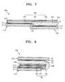
- FIG. 7is a cross-sectional view illustrating a multi-display apparatus 300 according to another embodiment.
- the same reference numeralsare used for elements which are identical to the elements shown in FIGS. 1 through 4 , and detailed descriptions thereof are omitted.
- a portion of a first substrate 311 of a first display panel 310, which overlaps with the second display panel 120is thinner than other areas of the first substrate 311.
- the first substrate 311includes two portions each having different thicknesses. As illustrated in FIG. 7 , a thickness of a portion of the first substrate 311 disposed above and overlapping a portion of the second display panel 120 is thinner than remaining portions of the first substrate 311. The portions of the first substrate 311 having the different thicknesses form a step portion at an area where the first substrate 311 overlaps the second display panel 120.
- a transparent plate 350is disposed directly adjacent to and surrounding a thin area of the first display panel 310, including a portion of a lower surface of the first display panel 310, and a side of the first display panel 310. As shown in FIG. 7 , the transparent plate 350 may extend to cover most of an upper surface of the first display panel 310, such as overlapping a whole of the first display devices 312. In a plan view, outer edges of the transparent plate 350 are spaced apart from the outer edges of the first and second display panels 310 and 120, respectively. The transparent plate 350 is not disposed adjacent to or overlapping with a lowermost surface of the first display panel 310 at thicker portions of the first substrate 311. In contrast, the transparent plate 150 in FIGS. 5 and 6 is disposed directly adjacent to and overlapping with a lowermost surface of the first display panel 110, which is effectively the lower surface of the first substrate 111.
- the transparent plate 350is disposed directly adjacent to an upper surface of a first protection cover 313 of the first display panel 310 so as to completely overlap a first display device 312, which is a light emitting area of the first display panel 310.
- first substrate 311 of the first display panel 310is thin in a boundary area between the first and second display panels 310 and 120, a stepped space formed by light emitting areas of the first and second display panels 310 and 120 may be decreased. Accordingly, a perpendicular stepped appearance resulting from the stepped space between the first and second display panels 310 and 120 may be reduced.
- FIG. 8is a cross-sectional view exemplarily illustrating a folded state of the multi-display apparatus 300 of FIG. 7 .
- the transparent plate 350 and the soft unit 193 of the transparent window 190include a flexible material, the multi-display apparatus 300 is foldable to dispose the first and second display panels 310 and 120 facing each other. Also, since the transparent plate 350 of FIG. 7 may be thinner than the transparent plate 150 of FIG. 2 , the multi-display apparatus 300 of FIG. 7 may be more easily folded.
- FIG. 9is a cross-sectional view illustrating a multi-display apparatus 400 according to another embodiment
- FIG. 10is a cross-sectional view exemplarily illustrating a folded state of the multi-display apparatus 400 of FIG. 9 .
- the same reference numeralsare used for elements which are identical to the elements shown in FIGS. 1 through 6 , and detailed descriptions thereof are omitted.
- the first substrate 411includes two portions each having different thicknesses. A thickness of a boundary portion of the first substrate 411 disposed overlapping with a portion of the second display panel 120 is thinner than in remaining areas of the first substrate 411.
- a transparent plate 450is disposed directly adjacent to and surrounds a thin area of the first display panel 410, including a portion of a lower surface and a side of the first display panel 410. As shown in FIG. 9 , the transparent plate 450 may extend to surround (e.g., overlap) most of an upper surface of the first display panel 410.
- the transparent plate 450is disposed directly adjacent to an upper surface of a first protection cover 413 of the first display panel 410 so as to completely overlap a first display device 412, which is a light emitting area of the first display panel 410.
- first substrate 411 of the first display panel 410is thin in the boundary area between the first display panel 410 and the second display panel 120, a stepped space formed by light emitting areas of the first and second display panels 410 and 120 is reduced. Accordingly, a perpendicular stepped appearance resulting from the stepped space between the first and second display panels 410 and 120 may be reduced.
- a transparent window 490includes hard (e.g., rigid) units 491 and 492, which are respectively disposed on the first and second display panels 410 and 120, and a soft (e.g., flexible or deformable) unit 493, which surrounds an entire of all outer surfaces of the hard units 491 and 492. Since the hard units 491 and 492 are essentially sealed inside the soft unit 493, an air gap does not exist in a boundary between the hard units 491 and 492 and the soft unit 493. Accordingly, a screen gap between the first and second display panels 410 and 120 is not generated since light is not diffused or refracted in the boundary between the hard units 491 and 492 and the soft unit 493.
- Thicknesses of the hard units 491 and 492 of the transparent window 490may be in a range of about 0.002 mm to about 2 mm, and a thickness of the soft unit 493 may be about 0.002 mm to about 2 mm thicker than the hard units 491 and 492. The thicknesses are taken in a direction of the perpendicular line 170.
- FIG. 11is a cross-sectional view illustrating a multi-display apparatus 500 according to another aspect of the invention.
- the same reference numeralsare used for elements which are identical to the elements shown in FIGS. 1 through 4 , and detailed descriptions thereof are omitted.
- the first substrate 111 of the first display panel 110is disposed to overlap with the second display panel 120.
- a transparent plate 550is disposed on the second display panel 120 to have the same height as an upper surface of the first display panel 110, and directly contacts one side of the first display panel 110. Unlike the embodiments in FIGS. 5-10 , no portion of the transparent plate 550 overlaps the first display panel 110 in a plan view.
- the transparent plate in FIG. 11is disposed overlapping only the second display panel 120 in the plan view.
- the transparent plate 550is disposed substantially coplanar with the upper surface of the first display panel 110, the upper surfaces form a continuous and planar surface.
- a thickness of the first display panel 110 and the transparent plate 550may be substantially the same, since both the first display panel and the transparent plate 550 are disposed on a same upper surface of the second display panel 120, while forming the continuous and planar upper surface.
- the transparent plate 550is a unitary indivisible and continuous member of the multi-display apparatus 500.
- first and second display panels 110 and 120are not separated by the transparent plate 550 and are disposed close together at a boundary area between the first and second display panels 110 and 120, a stepped space formed by light emitting areas of the first and second display panels 110 and 120 is reduced compared to the multi-display apparatus 100 of FIG. 2 . Accordingly, a perpendicular stepped appearance resulting from the stepped space between the first and second display panels 110 and 120 may be reduced.
- the transparent window 190includes the hard units 191 and 192, which protect the first and second display panels 110 and 120 and the transparent plate 150 from an external shock, and the soft unit 193, which is disposed between the hard units 191 and 192 on an area corresponding to the hinge axis H (refer to FIG. 1 ) in the plan view, so as to allow the first and second display panels 110 and 120 to fold.
- the structure and the operations of the multi-display apparatus 500may correspond to the structure and the operations of the multi-display apparatus 100 of FIGS. 1 through 4 , detailed descriptions thereof are omitted herein.
- a single, unitary and indivisible screen of a multi-display apparatus stretching over a plurality of display panelsis smoothly connected by reducing a perpendicular stepped appearance between the display panels, and the display panels are protected without hindering folding of the multi-display apparatus, by including a transparent window for shock prevention.
Landscapes
- Engineering & Computer Science (AREA)
- General Engineering & Computer Science (AREA)
- Theoretical Computer Science (AREA)
- Computer Hardware Design (AREA)
- Human Computer Interaction (AREA)
- Physics & Mathematics (AREA)
- General Physics & Mathematics (AREA)
- Multimedia (AREA)
- Signal Processing (AREA)
- Devices For Indicating Variable Information By Combining Individual Elements (AREA)
- Liquid Crystal (AREA)
Description
- One or more embodiments relate to a multi-display apparatus which realizes a screen by connecting a plurality of display panels, and more particularly, to a multi-display apparatus including the plurality of display panels connected in a folding method.
- A multi-display apparatus realizes one large screen by connecting a plurality of display panels. For example, a large screen is realized by connecting a plurality of cathode ray tubes ("CRTs") such as large televisions ("TVs"), for display.
- Such a multi-display apparatus is prepared by connecting unit display panels in a line. In other words, a multi-display screen is realized by connecting a plurality of unit display panels abreast of (e.g., directly adjacent to) each other. However, when the unit display panels are connected, an image at a joint between two display panels is not smoothly connected or displayed, and may appear badly broken. Also, a protection member for protecting the display panels, without a screen gap existing between the display panels, is required.
- United States Patent Application Publication Number
US 2008/0079656 A1 presents a multi-display device having first and second display panels closely in contact with each other. - An exemplary embodiment includes a multi-display apparatus including a protection member for protecting display panels without a screen gap existing between the display panels.
- An exemplary embodiment may include a multi-display apparatus including a first display panel, a second display panel disposed to overlap a portion of the first display panel, a transparent plate disposed overlapping a portion of both the first display panel and the second display panel, and a transparent window disposed on an area corresponding to the first display panel and the second display panel, wherein the transparent window defines an uppermost member of the combined structure including the first and the second display panels and the unitary indivisible transparent plate. The transparent window is bent when the multi-display apparatus is folded.
- The transparent window includes a first hard (e.g., rigid) unit and a second hard unit, which are spaced apart from each other respectively on the areas corresponding to the first display panel and the second display panel, and a soft unit disposed between the first hard unit and the second hard unit.
- The soft unit may surround at least a portion of the first hard unit and at least a portion of the second hard unit.
- The soft unit may surround entire surfaces of the first hard unit and the second hard unit, and thus the first hard unit and the second hard unit are contained by the soft unit.
- The soft unit may be about 0.002 millimeters (mm) to about 2 millimeters (mm thicker than the first and second hard units.
- A refractive index of the transparent window may be in a range of about 1.3 to about 1.7.
- The soft unit may be formed of at least one of tefron, a silicon resin, polymethyl methacrylate ("PMMA"), and polydimethylsiloxane ("PDMS").
- The first and second hard units may be formed of acryl or polycarbonate.
- The multi-display apparatus may further include an optical film disposed on an upper part of the transparent window.
- The optical film may be any one of an anti-reflection ("AR") film and an anti-glare ("AG") film.
- Each of the first and second display panels may include a substrate, a display device on the substrate, and a protection cover covering the display device.
- Refractive indexes of the protection cover, the transparent plate, and the transparent window may be in a range of about 1.3 to about 1.7.
- The display device may be any one of a liquid crystal display ("LCD"), a field emission display ("FED"), a plasma display panel ("PDP"), and an organic light-emitting diode ("OLED").
- A boundary area of the substrate of the first display panel overlapping with the second display panel may be thinner than other areas of the substrate of the first display panel.
- The transparent plate may surround a lower part of the boundary area of the substrate of the first display panel.
- The multi-display apparatus may be foldable around the soft unit.
- The transparent plate may be disposed on the second display panel to surround a lower surface and one side of the first display panel.
- The transparent plate may be disposed on the second display panel to surround a lower surface, an upper surface, and one side between the lower and upper surfaces of the first display panel.
- These and/or other aspects will become apparent and more readily appreciated from the following description of the embodiments, taken in conjunction with the accompanying drawings of which:
FIG. 1 is a perspective view illustrating a multi-display apparatus according to an embodiment;FIG. 2 is a cross-sectional view schematically illustrating the multi-display apparatus ofFIG. 1 ;FIGS. 3 and 4 are respectively a perspective view and a cross-sectional view exemplarily illustrating a folded state of the multi-display apparatus ofFIGS. 1 and 2 ;FIG. 5 is a cross-sectional view illustrating a multi-display apparatus according to another embodiment;FIG. 6 is a cross-sectional view illustrating a folded state of the multi-display apparatus ofFIG. 5 ;FIG. 7 is a cross-sectional view illustrating a multi-display apparatus according to another embodiment;FIG. 8 is a cross-sectional view exemplarily illustrating a folded state of the multi-display apparatus ofFIG. 7 ;FIG. 9 is a cross-sectional view illustrating a multi-display apparatus according to another embodiment;FIG. 10 is a cross-sectional view exemplarily illustrating a folded state of the multi-display apparatus ofFIG. 9 ; andFIG. 11 is a cross-sectional view illustrating a multi-display apparatus according to another aspect of the invention.- The invention is described more fully hereinafter with reference to the accompanying drawings, in which exemplary embodiments of the invention are shown. This invention may, however, be embodied in many different forms and should not be construed as limited to the exemplary embodiments set forth herein. Rather, these embodiments are provided so that this disclosure will be thorough and complete, and will fully convey the scope of the invention to those skilled in the art. In the drawings, the size and relative sizes of layers and regions may be exaggerated for clarity.
- It will be understood that when an element or layer is referred to as being "on" or "connected to" another element or layer, the element or layer can be directly on or connected to another element or layer or intervening elements or layers. In contrast, when an element is referred to as being "directly on" or "directly connected to" another element or layer, there are no intervening elements or layers present. As used herein, connected may refer to elements being physically and/or electrically connected to each other. Like numbers refer to like elements throughout. As used herein, the term "and/or" includes any and all combinations of one or more of the associated listed items.
- It will be understood that, although the terms first, second, third, etc., may be used herein to describe various elements, components, regions, layers and/or sections, these elements, components, regions, layers and/or sections should not be limited by these terms. These terms are only used to distinguish one element, component, region, layer or section from another region, layer or section. Thus, a first element, component, region, layer or section discussed below could be termed a second element, component, region, layer or section without departing from the teachings of the exemplary embodiments.
- Spatially relative terms, such as "lower," "upper" and the like, may be used herein for ease of description to describe the relationship of one element or feature to another element(s) or feature(s) as illustrated in the figures. It will be understood that the spatially relative terms are intended to encompass different orientations of the device in use or operation, in addition to the orientation depicted in the figures. For example, if the device in the figures is turned over, elements described as "lower" relative to other elements or features would then be oriented "upper" relative to the other elements or features. Thus, the exemplary term "lower" can encompass both an orientation of above and below. The device may be otherwise oriented (rotated 90 degrees or at other orientations) and the spatially relative descriptors used herein interpreted accordingly.
- The terminology used herein is for the purpose of describing particular embodiments only and is not intended to be limiting of the invention. As used herein, the singular forms "a", "an" and "the" are intended to include the plural forms as well, unless the context clearly indicates otherwise. It will be further understood that the terms "comprises" and/or "comprising," when used in this specification, specify the presence of stated features, integers, steps, operations, elements, and/or components, but do not preclude the presence or addition of one or more other features, integers, steps, operations, elements, components, and/or groups thereof.
- Embodiments of the invention are described herein with reference to cross-section illustrations that are schematic illustrations of idealized embodiments (and intermediate structures) of the invention. As such, variations from the shapes of the illustrations as a result, for example, of manufacturing techniques and/or tolerances, are to be expected. Thus, embodiments of the invention should not be construed as limited to the particular shapes of regions illustrated herein but are to include deviations in shapes that result, for example, from manufacturing.
- Unless otherwise defined, all terms (including technical and scientific terms) used herein have the same meaning as commonly understood by one of ordinary skill in the art to which this invention belongs. It will be further understood that terms, such as those defined in commonly used dictionaries, should be interpreted as having a meaning that is consistent with their meaning in the context of the relevant art and will not be interpreted in an idealized or overly formal sense unless expressly so defined herein.
- Reference will now be made in detail to embodiments, examples of which are illustrated in the accompanying drawings. In this regard, the exemplary embodiments may have different forms and should not be construed as being limited to the descriptions set forth herein. Accordingly, the embodiments are merely described below, by referring to the figures, to explain aspects of the detailed description.
FIGS. 1 and 2 are diagrams illustrating amulti-display apparatus 100 according to an embodiment. Themulti-display apparatus 100 may be formed by connecting a plurality of display panels by using any of a variety of methods, but for convenience of description, afirst display panel 110 and asecond display panel 120 are connected in the illustrated embodiment. Afirst display device 112 and asecond display device 122, which realize images, are illustrated in brief.- Two display panels are connected in
FIGS. 1 and 2 , but the same principle may be applied when a screen is realized by connecting three or more display panels. - The
multi-display apparatus 100 includes abody 180 which includes afirst part 181, asecond part 182, and ahinge unit 183 connecting the first andsecond parts hinge unit 183. In order to realize images, as illustrated inFIG. 2 , the first andsecond display panels second display devices second substrates second display panels second display devices second display devices second display panels - Accordingly, when the
multi-display apparatus 100 is an upward light emitting type, images prepared by the first andsecond display devices multi-display apparatus 100 is a downward light emitting type, the images are displayed through the first andsecond substrates multi-display apparatus 100 illustrated inFIGS. 1 and 2 is an upward light emitting type. The first andsecond display devices second display panels - The first and
second display panels multi-display apparatus 100 by being connected to each other in a folding method, whereby themulti-display apparatus 100 is folded and unfolded centering around the hinge axis H, as illustrated inFIG. 1 . When the first andsecond display panels second display panels second display panels FIG. 2 , when themulti-display apparatus 100 is unfolded. When boundary surfaces (e.g., edges) of the first andsecond display devices perpendicular line 170 by overlapping the first andsecond display panels multi-display apparatus 100 seems to be continuous when viewed from a perpendicular direction. - However, a perpendicular stepped appearance resulting from the stepped space between the first and
second display panels multi-display apparatus 100 may include atransparent plate 150 disposed on an upper portion of thesecond display panel 120. Thetransparent plate 150 may be extended to cover (e.g., overlap) an upper portion of thefirst display panel 110. In the illustrated embodiment, thetransparent plate 150 may be disposed to overlap aside 126 and alower surface 127 of thefirst display panel 110. Thetransparent plate 150 is a unitary indivisible and continuous member of themulti-display apparatus 100. - In
FIG. 2 , thetransparent plate 150 is disposed to cover an upper surface of thefirst display panel 110, where the upper surface of thefirst display panel 110 is separated from an upper surface of thetransparent plate 150. Alternatively, thetransparent plate 150 may have a same height as thefirst display panel 110, such that the upper surfaces of thefirst display panel 110 and thetransparent plate 150 are coplanar with each other. The upper surface and a lower surface of thetransparent plate 150 are continuous and planar. - In order to protect the first and
second display panels transparent plate 150 from an external shock, themulti-display apparatus 100 according to an embodiment may further include atransparent window 190 for shock prevention disposed on the upper parts of the first andsecond display panels transparent window 190 may define an uppermost member of the combined structure including the first andsecond display panels transparent plate 150, but the invention is not limited thereto. - The
transparent window 190 includes hard (e.g. rigid)units second display panels transparent plate 150 from an external shock, and a transparent soft (e.g., flexible or deformable)unit 193 disposed between thehard units multi-display apparatus 100 to fold such that the first andsecond display panels transparent window 190 are continuous and planar. As used herein, "corresponding" may refer to as being related in position, dimension and/or shape to another element. - The
transparent plate 150 may include a soft material which is flexible and can be elastically restored after it is deformed, so that themulti-display apparatus 100 is foldable to dispose the first andsecond display panels - The
soft unit 193 may include a polymer material which is flexible and can be elastically restored after it is deformed. For example, thesoft unit 193 may include any one of polymethyl methacrylate ("PMMA"), polydimethylsiloxane ("PDMS"), a transparent silicon resin, and teflon. - The
hard units - A thickness of the
transparent plate 150 may change according to a thickness of thefirst display panel 110. The thickness of thetransparent plate 150 is taken in a direction of theperpendicular line 170 shown inFIG. 2 . The thickness of thefirst display panel 110 may be in a range of about 0.01 millimeters (mm) to about 3 mm, and thetransparent plate 150 may be about 0.002 mm to about 2 mm thicker than thefirst display panel 110. In detail, a portion of thetransparent plate 150 which surrounds thefirst display panel 110, for example, a portion adjacent to theside 126, may have a thickness in a range of about 0.001 mm to about 1 mm further than the upper orlower surface 127 of thefirst display panel 110. A portion of thetransparent plate 150 which extends over and overlaps an upper surface of thesecond display panel 120 may have a thickness in a range of about 0.012 mm to about 5 mm. - Refractive indexes of the
first protection cover 113 of thefirst display panel 110 and thetransparent plate 150 may be substantially the same, so that light is not refracted on an interface between thefirst protection cover 113 and thetransparent plate 150. Alternatively, the refractive indexes of thefirst protection cover 113 and thetransparent plate 150 may not be the same, but may be similar so that the light is barely refracted. In an exemplary embodiment, the refractive index of thetransparent plate 150 may be in a range of about 1.3 to about 1.7. - In order to improve the performance of the
multi-display apparatus 100 according to the usage of themulti-display apparatus 100, anoptical film 195 may be attached to the upper portion of thetransparent plate 150, such as being disposed directly on and contacting an upper surface of thetransparent window 190. In one exemplary embodiment, a polarizing film, an anti-reflection ("AR") film, or an anti-glare ("AG") film may be disposed on an entire of the upper surface of thetransparent plate 150. Theoptical film 195 may define an uppermost member of the combined structure including the first andsecond display panels transparent plate 150 and thetransparent window 190 as illustrated inFIG. 2 . - A thickness of the
transparent window 190 may be in a range of about 0.002 mm to about 2 mm. The thickness is taken in a direction of theperpendicular line 170, shown inFIG. 2 . FIGS. 3 and 4 are respectively a perspective view and a cross-sectional view exemplarily illustrating a folded state of themulti-display apparatus 100 ofFIGS. 1 and 2 . InFIG. 3 , an internal folded state of the first andsecond display panels transparent window 190 are not shown. Thebody 180 including thefirst part 181, thesecond part 182, and thehinge unit 183 effectively forms an outermost member of themulti-display apparatus 100. The combined structure of the first andsecond display panels body 180, as illustrated inFIGS. 1 and3 .- Referring to
FIG. 4 , since thetransparent window 190 includes thesoft unit 193 in an area corresponding to the hinge axis H, and thetransparent plate 150 includes a flexible material, themulti-display apparatus 100 is easily folded to disposed the first andsecond display panels FIG. 4 , thetransparent window 190 and thetransparent plate 150 are illustrated as being relatively very thick, but since thetransparent window 190 and thetransparent plate 150 are thin, themulti-display apparatus 100 can be folded. - In an exemplary embodiment in order to adjust the refractive index of the
soft unit 193, a suitable additive may be further added to a material of thesoft unit 193. FIG. 5 is a cross-sectional view illustrating amulti-display apparatus 200 according to another embodiment. The same reference numerals are used for elements which are identical to the elements shown inFIGS. 1 through 4 , and detailed descriptions thereof are omitted.- Referring to
FIG. 5 , atransparent window 290 includes hard (e.g., rigid)units second display panels unit 293 surrounding an entire of all outer surfaces of both thehard units hard units soft unit 293, an air gap does not exist in a boundary between thehard units soft unit 293. Accordingly, a screen gap between the first andsecond display panels hard units soft unit 293. - Thicknesses of the
hard units soft unit 293 may be about 0.002 mm to about 2 mm thicker than thehard units perpendicular line 170. - Since the
multi-display apparatus 200 is substantially identical to themulti-display apparatus 100 except for a structure of thetransparent window 290, detailed descriptions thereof are omitted herein.FIG. 6 is a cross-sectional view illustrating a folded state of themulti-display apparatus 200 ofFIG. 5 . Since thesoft unit 293 is disposed between thehard units transparent plate 150 and thetransparent window 290 are bent, themulti-display apparatus 200 is easily folded to dispose the first andsecond display panels FIG. 7 is a cross-sectional view illustrating amulti-display apparatus 300 according to another embodiment. The same reference numerals are used for elements which are identical to the elements shown inFIGS. 1 through 4 , and detailed descriptions thereof are omitted.- Referring to
FIG. 7 , a portion of afirst substrate 311 of afirst display panel 310, which overlaps with thesecond display panel 120 is thinner than other areas of thefirst substrate 311. In other words, thefirst substrate 311 includes two portions each having different thicknesses. As illustrated inFIG. 7 , a thickness of a portion of thefirst substrate 311 disposed above and overlapping a portion of thesecond display panel 120 is thinner than remaining portions of thefirst substrate 311. The portions of thefirst substrate 311 having the different thicknesses form a step portion at an area where thefirst substrate 311 overlaps thesecond display panel 120. - A
transparent plate 350 is disposed directly adjacent to and surrounding a thin area of thefirst display panel 310, including a portion of a lower surface of thefirst display panel 310, and a side of thefirst display panel 310. As shown inFIG. 7 , thetransparent plate 350 may extend to cover most of an upper surface of thefirst display panel 310, such as overlapping a whole of thefirst display devices 312. In a plan view, outer edges of thetransparent plate 350 are spaced apart from the outer edges of the first andsecond display panels transparent plate 350 is not disposed adjacent to or overlapping with a lowermost surface of thefirst display panel 310 at thicker portions of thefirst substrate 311. In contrast, thetransparent plate 150 inFIGS. 5 and 6 is disposed directly adjacent to and overlapping with a lowermost surface of thefirst display panel 110, which is effectively the lower surface of thefirst substrate 111. - The
transparent plate 350 is disposed directly adjacent to an upper surface of afirst protection cover 313 of thefirst display panel 310 so as to completely overlap afirst display device 312, which is a light emitting area of thefirst display panel 310. - Since the
first substrate 311 of thefirst display panel 310 is thin in a boundary area between the first andsecond display panels second display panels second display panels FIG. 8 is a cross-sectional view exemplarily illustrating a folded state of themulti-display apparatus 300 ofFIG. 7 . Since thetransparent plate 350 and thesoft unit 193 of thetransparent window 190 include a flexible material, themulti-display apparatus 300 is foldable to dispose the first andsecond display panels transparent plate 350 ofFIG. 7 may be thinner than thetransparent plate 150 ofFIG. 2 , themulti-display apparatus 300 ofFIG. 7 may be more easily folded.FIG. 9 is a cross-sectional view illustrating amulti-display apparatus 400 according to another embodiment, andFIG. 10 is a cross-sectional view exemplarily illustrating a folded state of themulti-display apparatus 400 ofFIG. 9 . The same reference numerals are used for elements which are identical to the elements shown inFIGS. 1 through 6 , and detailed descriptions thereof are omitted.- Referring to
FIGS. 9 and 10 , a portion of afirst substrate 411 of afirst display panel 410, which overlaps with thesecond display panel 120, is thinner than other areas of thefirst substrate 411. In other words, thefirst substrate 411 includes two portions each having different thicknesses. A thickness of a boundary portion of thefirst substrate 411 disposed overlapping with a portion of thesecond display panel 120 is thinner than in remaining areas of thefirst substrate 411. - A
transparent plate 450 is disposed directly adjacent to and surrounds a thin area of thefirst display panel 410, including a portion of a lower surface and a side of thefirst display panel 410. As shown inFIG. 9 , thetransparent plate 450 may extend to surround (e.g., overlap) most of an upper surface of thefirst display panel 410. - The
transparent plate 450 is disposed directly adjacent to an upper surface of afirst protection cover 413 of thefirst display panel 410 so as to completely overlap afirst display device 412, which is a light emitting area of thefirst display panel 410. - Since the
first substrate 411 of thefirst display panel 410 is thin in the boundary area between thefirst display panel 410 and thesecond display panel 120, a stepped space formed by light emitting areas of the first andsecond display panels second display panels - A
transparent window 490 includes hard (e.g., rigid)units second display panels unit 493, which surrounds an entire of all outer surfaces of thehard units hard units soft unit 493, an air gap does not exist in a boundary between thehard units soft unit 493. Accordingly, a screen gap between the first andsecond display panels hard units soft unit 493. - Thicknesses of the
hard units transparent window 490 may be in a range of about 0.002 mm to about 2 mm, and a thickness of thesoft unit 493 may be about 0.002 mm to about 2 mm thicker than thehard units perpendicular line 170. FIG. 11 is a cross-sectional view illustrating amulti-display apparatus 500 according to another aspect of the invention. The same reference numerals are used for elements which are identical to the elements shown inFIGS. 1 through 4 , and detailed descriptions thereof are omitted.- Referring to
FIG. 11 , thefirst substrate 111 of thefirst display panel 110 is disposed to overlap with thesecond display panel 120. Atransparent plate 550 is disposed on thesecond display panel 120 to have the same height as an upper surface of thefirst display panel 110, and directly contacts one side of thefirst display panel 110. Unlike the embodiments inFIGS. 5-10 , no portion of thetransparent plate 550 overlaps thefirst display panel 110 in a plan view. The transparent plate inFIG. 11 is disposed overlapping only thesecond display panel 120 in the plan view. - Where an upper surface of the
transparent plate 550 is disposed substantially coplanar with the upper surface of thefirst display panel 110, the upper surfaces form a continuous and planar surface. A thickness of thefirst display panel 110 and thetransparent plate 550 may be substantially the same, since both the first display panel and thetransparent plate 550 are disposed on a same upper surface of thesecond display panel 120, while forming the continuous and planar upper surface. Thetransparent plate 550 is a unitary indivisible and continuous member of themulti-display apparatus 500. - Since the first and
second display panels transparent plate 550 and are disposed close together at a boundary area between the first andsecond display panels second display panels multi-display apparatus 100 ofFIG. 2 . Accordingly, a perpendicular stepped appearance resulting from the stepped space between the first andsecond display panels - The
transparent window 190 includes thehard units second display panels transparent plate 150 from an external shock, and thesoft unit 193, which is disposed between thehard units FIG. 1 ) in the plan view, so as to allow the first andsecond display panels - Since the structure and the operations of the
multi-display apparatus 500 may correspond to the structure and the operations of themulti-display apparatus 100 ofFIGS. 1 through 4 , detailed descriptions thereof are omitted herein. - As described above, according to the one or more of the above embodiments, a single, unitary and indivisible screen of a multi-display apparatus stretching over a plurality of display panels is smoothly connected by reducing a perpendicular stepped appearance between the display panels, and the display panels are protected without hindering folding of the multi-display apparatus, by including a transparent window for shock prevention.
- It should be understood that the exemplary embodiments described herein should be considered in a descriptive sense only and not for purposes of limitation. Descriptions of features or aspects within each embodiment should typically be considered as available for other similar features or aspects in other embodiments.
Claims (14)
- A multi-display apparatus (100) comprising:a first display panel (110);a second display panel (120) disposed to overlap a portion of the first display panel in a plan view of the multi-display apparatus;a unitary indivisible transparent plate (150) disposed overlapping a portion of both the first display panel and the second display panel, the unitary indivisible transparent plate (150) including a soft material which is flexible so that the multi-display apparatus (100) is foldable to dispose the first display panel (110) facing the second display panel (120); anda transparent window (190) disposed overlapping both the first display panel and the second display panel, wherein the transparent window (190) defines an uppermost member of the combined structure including the first and the second display panels (110, 120) and the unitary indivisible transparent plate (150), the transparent window comprising a first rigid unit (191) and a second rigid unit (192), which are spaced apart from each other in the plan view, the first rigid unit and the second rigid unit being respectively disposed on areas corresponding to the first display panel (110) and the second display panel (120), and a soft unit (193) disposed between the first rigid unit and the second rigid unit such that the transparent window is bendable when the multi-display apparatus is folded to dispose the first display panel facing the second display panel.
- The multi-display apparatus of claim 1, wherein the soft unit (193) surrounds at least a portion of the first rigid unit (191) and at least a portion of the second rigid unit (192), or wherein the soft unit (193) is disposed adjacent to an entire of all outer surfaces of the first rigid unit (191) and the second rigid unit (192), such that the first rigid unit and the second rigid unit are surrounded by the soft unit.
- The multi-display apparatus of claim 2, wherein a thickness of the soft unit (193) is about 0.002 millimeters to about 2 millimeters larger than thicknesses of both the first (191) and second (192) rigid units, the thicknesses taken perpendicular to an upper surface of the transparent window (190).
- The multi-display apparatus of claim 1, wherein a refractive index of the transparent window (190) is in a range of about 1.3 to about 1.7.
- The multi-display apparatus of claim 1, wherein the soft unit (193) includes at least one of teflon, a silicon resin, polymethyl methacrylate ("PMMA"), and polydimethylsiloxane ("PDMS").
- The multi-display apparatus of claim 1, wherein the first (191) and second (192) rigid units include acryl or polycarbonate.
- The multi-display apparatus of claim 1, further comprising an optical film (195) disposed directly on an upper surface of the transparent window (190)
- The multi-display apparatus of claim 7, wherein the optical film (195) is any one of an anti-reflection film and an anti-glare film.
- The multi-display apparatus of claim 1, wherein each of the first (110) and second (120) display panels comprises a substrate, a display device on the substrate, and a protection cover disposed overlapping an entire of the display device, and wherein refractive indexes of the protection cover, the transparent plate, and the transparent window are in a range of about 1.3 to about 1.7.
- The multi-display apparatus of claim 9, wherein the display device is any one of a liquid crystal display, a field emission display, a plasma display panel, and an organic light-emitting diode.
- The multi-display apparatus of claim 9, wherein a thickness of a portion of the substrate of the first display panel (110) overlapping with the second display panel (120) in the plan view, is smaller than a thickness of remaining portions of the substrate of the first display panel not overlapping with the second display panel, and wherein a portion of the transparent plate (150) is disposed between the thinner portion of the substrate of the first display panel overlapping with the second display panel, and the second display panel.
- The multi-display apparatus of claim 1, wherein the soft unit (193) is disposed directly adjacent to an entire of all outer surfaces of both the first and second rigid units, such that the first and second rigid units are surrounded by the soft unit.
- The multi-display apparatus of claim 1, wherein the multi-display apparatus is foldable around the soft unit (193) to dispose the first display panel (110) facing the second display panel (120).
- The multi-display apparatus of claim 1, wherein the transparent plate (150) is disposed on the second display panel (120), and directly adjacent to both a lower surface, and one side of the first display panel (110) connecting the lower and an upper surface of the first display panel, and wherein the transparent plate (150) is disposed directly adjacent to the upper surface of the first display panel (110).
Applications Claiming Priority (1)
| Application Number | Priority Date | Filing Date | Title |
|---|---|---|---|
| KR1020090011499AKR101563685B1 (en) | 2009-02-12 | 2009-02-12 | Multi-display apparatus |
Publications (3)
| Publication Number | Publication Date |
|---|---|
| EP2219096A2 EP2219096A2 (en) | 2010-08-18 |
| EP2219096A3 EP2219096A3 (en) | 2012-06-06 |
| EP2219096B1true EP2219096B1 (en) | 2015-02-25 |
Family
ID=41509808
Family Applications (1)
| Application Number | Title | Priority Date | Filing Date |
|---|---|---|---|
| EP09178536.0AActiveEP2219096B1 (en) | 2009-02-12 | 2009-12-09 | Multi-display apparatus |
Country Status (3)
| Country | Link |
|---|---|
| US (1) | US8659503B2 (en) |
| EP (1) | EP2219096B1 (en) |
| KR (1) | KR101563685B1 (en) |
Families Citing this family (36)
| Publication number | Priority date | Publication date | Assignee | Title |
|---|---|---|---|---|
| US20120081315A1 (en) | 2010-10-01 | 2012-04-05 | Imerj LLC | Keyboard spanning multiple screens |
| KR101457563B1 (en)* | 2008-11-11 | 2014-11-04 | 삼성전자주식회사 | Multi-display device |
| US20120236484A1 (en)* | 2009-12-01 | 2012-09-20 | Hideyuki Miyake | Foldable mobile terminal |
| KR101713277B1 (en)* | 2010-08-13 | 2017-03-08 | 삼성전자주식회사 | Anti-reflection film and foldable display apparatus employing the same |
| KR101720588B1 (en)* | 2010-12-07 | 2017-03-30 | 삼성전자주식회사 | Foldable organic light emitting diode display |
| KR101672345B1 (en) | 2010-12-08 | 2016-11-04 | 삼성전자주식회사 | Foldable display apparatus |
| KR101799520B1 (en)* | 2011-02-01 | 2017-11-21 | 삼성전자 주식회사 | Folderble display apparatus |
| US9927839B2 (en)* | 2011-05-03 | 2018-03-27 | DISH Technologies L.L.C. | Communications device with extendable screen |
| KR102127980B1 (en)* | 2013-05-10 | 2020-06-29 | 삼성전자주식회사 | Portable electrinic device having dual display |
| KR102039496B1 (en) | 2013-08-19 | 2019-11-04 | 삼성디스플레이 주식회사 | Foldable display device |
| KR102206376B1 (en)* | 2013-09-24 | 2021-01-22 | 삼성디스플레이 주식회사 | Cover window for display device, display device comprising the same |
| KR20150049838A (en)* | 2013-10-31 | 2015-05-08 | 삼성디스플레이 주식회사 | Composite film, method of manufacturing the composite film and apparatus for performing the method |
| KR102154833B1 (en) | 2014-01-28 | 2020-09-11 | 삼성디스플레이 주식회사 | Flexible display device |
| KR102251081B1 (en) | 2014-02-05 | 2021-05-13 | 삼성디스플레이 주식회사 | Flexible display apparatus |
| US9588549B2 (en) | 2014-02-28 | 2017-03-07 | Semiconductor Energy Laboratory Co., Ltd. | Electronic device |
| KR102384830B1 (en)* | 2014-03-12 | 2022-04-07 | 가부시키가이샤 한도오따이 에네루기 켄큐쇼 | Display device and data processing device |
| KR102243206B1 (en)* | 2014-03-18 | 2021-04-23 | 삼성디스플레이 주식회사 | Flexible display device |
| KR102155252B1 (en)* | 2014-07-01 | 2020-09-11 | 엘지디스플레이 주식회사 | Organic light emitting display device and method of manufacturing the same |
| KR101794872B1 (en)* | 2014-09-28 | 2017-11-09 | 주식회사 가난한동지들 | Flexible display apparatus with ability of over unfolding more than complete plane forming angle |
| KR102346955B1 (en) | 2015-01-30 | 2022-01-04 | 삼성디스플레이 주식회사 | Flexible window substrate and flexible display device having the same |
| KR102305462B1 (en) | 2015-04-30 | 2021-09-27 | 삼성디스플레이 주식회사 | Flexible window substrate and flexible display device having the same |
| KR101673862B1 (en)* | 2015-05-21 | 2016-11-08 | 한국생산기술연구원 | Transparent electrode film for OLED, transparent OLED device and method for manufacturing thereof |
| KR102405121B1 (en) | 2015-11-13 | 2022-06-08 | 삼성디스플레이 주식회사 | Foldable display apparatus |
| KR102431709B1 (en)* | 2015-12-21 | 2022-08-12 | 삼성디스플레이 주식회사 | Multi-display apparatus |
| KR102433269B1 (en)* | 2016-01-18 | 2022-08-17 | 삼성전자 주식회사 | Flexible Display Device and Display Control Method Thereof |
| KR102487920B1 (en)* | 2016-05-03 | 2023-01-13 | 삼성전자주식회사 | Foldable display device |
| CN105974632B (en)* | 2016-07-15 | 2019-04-30 | 武汉华星光电技术有限公司 | Folding liquid crystal display and preparation method thereof |
| KR102170496B1 (en)* | 2017-08-26 | 2020-10-28 | 주식회사 가난한동지들 | Flexible display apparatus with ability of over unfolding more than complete plane forming angle |
| KR102407767B1 (en)* | 2017-10-19 | 2022-06-10 | 엘지디스플레이 주식회사 | Foldable display apparatus |
| US10936343B2 (en) | 2018-04-18 | 2021-03-02 | Microsoft Technology Licensing, Llc | In-context event orchestration of physical and cyber resources |
| USD945993S1 (en)* | 2018-05-29 | 2022-03-15 | Intel Corporation | Hinged electronic device |
| WO2020044171A1 (en) | 2018-08-31 | 2020-03-05 | 株式会社半導体エネルギー研究所 | Display device |
| CN109979413B (en)* | 2019-03-18 | 2021-02-02 | Oppo广东移动通信有限公司 | Screen-lighting control method, screen-lighting control device, electronic equipment and readable storage medium |
| KR102668705B1 (en)* | 2019-03-21 | 2024-05-23 | 삼성디스플레이 주식회사 | Display device and method of fabricating the same |
| JP7572143B2 (en)* | 2019-03-29 | 2024-10-23 | 大日本印刷株式会社 | Optical film and image display device |
| KR20220075023A (en)* | 2020-11-26 | 2022-06-07 | 삼성디스플레이 주식회사 | Display device and method for manufacturing the same, tiled display device comprising the same |
Family Cites Families (23)
| Publication number | Priority date | Publication date | Assignee | Title |
|---|---|---|---|---|
| FR2632610B3 (en)* | 1988-06-10 | 1990-10-19 | Dupuy Eng Sa | METHOD FOR MANUFACTURING SHEETS FOR COVERING WINDOWS FROM FOLDABLE DISPLAY BOXES, WINDOWS MADE THEREOF AND PACKAGING BOXES PROVIDED WITH SUCH WINDOWS |
| GB8819647D0 (en)* | 1988-08-18 | 1988-09-21 | Alcatel Business Systems | Franking machine |
| US5734513A (en)* | 1996-04-03 | 1998-03-31 | Industrial Technology Research Institute | Electronic apparatus with a foldable display |
| DE19782261C2 (en)* | 1997-12-24 | 2002-12-12 | Mitsubishi Electric Corp | Attachment construction for a flexible liquid crystal display panel |
| WO2002025362A1 (en)* | 2000-09-19 | 2002-03-28 | Si Han Kim | Multi display device |
| KR100365311B1 (en) | 2000-11-22 | 2002-12-18 | 김시환 | Case of folder type multi display device |
| TW579019U (en)* | 2001-06-13 | 2004-03-01 | Eturbotouch Technology Inc | Flexible current type touch film |
| US20030026068A1 (en)* | 2001-07-31 | 2003-02-06 | Wen-Sung Tsai | Portable computing device with foldable display panels |
| JP2003208112A (en)* | 2002-01-11 | 2003-07-25 | Fuji Xerox Co Ltd | Image display device |
| CA2551595C (en)* | 2003-12-26 | 2011-02-08 | Nissha Printing Co., Ltd. | Electronic device with protection panel, protection panel, and method offabricating protection panels |
| CN100452113C (en)* | 2004-02-20 | 2009-01-14 | 日本写真印刷株式会社 | Protection panel for electronic apparatus display window and production method for protection panel |
| JP5005164B2 (en)* | 2004-03-03 | 2012-08-22 | 株式会社ジャパンディスプレイイースト | LIGHT EMITTING ELEMENT, LIGHT EMITTING DISPLAY DEVICE AND LIGHTING DEVICE |
| KR20060020317A (en) | 2004-08-31 | 2006-03-06 | 엘지.필립스 엘시디 주식회사 | LCD Display |
| KR100706676B1 (en) | 2004-12-13 | 2007-04-11 | 엘지.필립스 엘시디 주식회사 | Mobile terminal with folding liquid crystal display screen |
| KR20070003295A (en) | 2005-07-01 | 2007-01-05 | 삼성전자주식회사 | Indicator protective cover |
| US20070010303A1 (en)* | 2005-07-05 | 2007-01-11 | Nokia Corporation | High quality optical windows for mobile phones and cameras |
| WO2007043700A1 (en) | 2005-10-14 | 2007-04-19 | Fujifilm Corporation | Anti-reflection film, and polarizing plate and image display device using the same |
| KR101217554B1 (en) | 2006-05-09 | 2013-01-02 | 삼성전자주식회사 | seamless foldable display device |
| ITRM20060355A1 (en) | 2006-07-06 | 2008-01-07 | Keymat Ind S P A | SUPPORT AND PROTECTION DEVICE FOR A DISPLAY SCREEN DISPLAY DEVICE AS AN EXAMPLE OF LCD |
| KR101217558B1 (en)* | 2006-09-29 | 2013-01-02 | 삼성전자주식회사 | Multi-display apparatus |
| KR20080030262A (en) | 2006-09-29 | 2008-04-04 | 삼성전자주식회사 | Multi display device |
| TWI361919B (en)* | 2006-10-27 | 2012-04-11 | Ind Tech Res Inst | Driving method of liquid crystal display panel |
| WO2008069221A1 (en)* | 2006-12-05 | 2008-06-12 | Semiconductor Energy Laboratory Co., Ltd. | Plasma display panel and field emission display |
- 2009
- 2009-02-12KRKR1020090011499Apatent/KR101563685B1/enactiveActive
- 2009-08-27USUS12/548,503patent/US8659503B2/ennot_activeExpired - Fee Related
- 2009-12-09EPEP09178536.0Apatent/EP2219096B1/enactiveActive
Also Published As
| Publication number | Publication date |
|---|---|
| KR101563685B1 (en) | 2015-10-28 |
| EP2219096A3 (en) | 2012-06-06 |
| KR20100092220A (en) | 2010-08-20 |
| EP2219096A2 (en) | 2010-08-18 |
| US8659503B2 (en) | 2014-02-25 |
| US20100201603A1 (en) | 2010-08-12 |
Similar Documents
| Publication | Publication Date | Title |
|---|---|---|
| EP2219096B1 (en) | Multi-display apparatus | |
| US20100201604A1 (en) | Multi-foldable mobile display apparatus | |
| US8582049B2 (en) | Foldable display apparatus | |
| US11307613B2 (en) | Display device | |
| EP2184662B1 (en) | Multi-display apparatus | |
| US8593372B2 (en) | Foldable display device | |
| KR101217558B1 (en) | Multi-display apparatus | |
| US9442316B2 (en) | Display device comprising a light-transmitting cover having a lens portion | |
| US8760365B2 (en) | Multi-display apparatus and method thereof | |
| EP3671703B1 (en) | Foldable cover plate, foldable display module, and foldable terminal device | |
| US11886243B2 (en) | Display device | |
| US20210234107A1 (en) | Foldable display device | |
| US11726527B2 (en) | Display device | |
| US11526196B2 (en) | Display device | |
| US20220059795A1 (en) | Display device | |
| KR102854996B1 (en) | Foldable display device | |
| CN114078379A (en) | Display device and method for manufacturing display device | |
| KR101810049B1 (en) | Flexible display panel and the display apparatus comprising the flexible display panel | |
| US11626565B2 (en) | Display device | |
| KR20080079089A (en) | Multi display device | |
| US20080144173A1 (en) | Multi-display apparatus and method of manufacturing thereof | |
| CN117437850A (en) | Flexible display device and metal plate | |
| US20240107858A1 (en) | Display device | |
| US20240306353A1 (en) | Display device |
Legal Events
| Date | Code | Title | Description |
|---|---|---|---|
| PUAI | Public reference made under article 153(3) epc to a published international application that has entered the european phase | Free format text:ORIGINAL CODE: 0009012 | |
| AK | Designated contracting states | Kind code of ref document:A2 Designated state(s):AT BE BG CH CY CZ DE DK EE ES FI FR GB GR HR HU IE IS IT LI LT LU LV MC MK MT NL NO PL PT RO SE SI SK SM TR | |
| AX | Request for extension of the european patent | Extension state:AL BA RS | |
| PUAL | Search report despatched | Free format text:ORIGINAL CODE: 0009013 | |
| AK | Designated contracting states | Kind code of ref document:A3 Designated state(s):AT BE BG CH CY CZ DE DK EE ES FI FR GB GR HR HU IE IS IT LI LT LU LV MC MK MT NL NO PL PT RO SE SI SK SM TR | |
| AX | Request for extension of the european patent | Extension state:AL BA RS | |
| RIC1 | Information provided on ipc code assigned before grant | Ipc:H04N 5/64 20060101ALI20120427BHEP Ipc:G06F 1/16 20060101AFI20120427BHEP | |
| RAP1 | Party data changed (applicant data changed or rights of an application transferred) | Owner name:SAMSUNG MOBILE DISPLAY CO., LTD. Owner name:SAMSUNG ELECTRONICS CO., LTD. | |
| RAP1 | Party data changed (applicant data changed or rights of an application transferred) | Owner name:SAMSUNG DISPLAY CO., LTD. Owner name:SAMSUNG ELECTRONICS CO., LTD. | |
| 17P | Request for examination filed | Effective date:20121206 | |
| 17Q | First examination report despatched | Effective date:20130122 | |
| RIC1 | Information provided on ipc code assigned before grant | Ipc:H04N 9/12 20060101ALI20131122BHEP Ipc:G06F 1/16 20060101AFI20131122BHEP | |
| GRAP | Despatch of communication of intention to grant a patent | Free format text:ORIGINAL CODE: EPIDOSNIGR1 | |
| INTG | Intention to grant announced | Effective date:20140225 | |
| GRAS | Grant fee paid | Free format text:ORIGINAL CODE: EPIDOSNIGR3 | |
| GRAP | Despatch of communication of intention to grant a patent | Free format text:ORIGINAL CODE: EPIDOSNIGR1 | |
| INTG | Intention to grant announced | Effective date:20140724 | |
| GRAS | Grant fee paid | Free format text:ORIGINAL CODE: EPIDOSNIGR3 | |
| GRAA | (expected) grant | Free format text:ORIGINAL CODE: 0009210 | |
| AK | Designated contracting states | Kind code of ref document:B1 Designated state(s):AT BE BG CH CY CZ DE DK EE ES FI FR GB GR HR HU IE IS IT LI LT LU LV MC MK MT NL NO PL PT RO SE SI SK SM TR | |
| REG | Reference to a national code | Ref country code:GB Ref legal event code:FG4D | |
| REG | Reference to a national code | Ref country code:CH Ref legal event code:EP | |
| REG | Reference to a national code | Ref country code:IE Ref legal event code:FG4D | |
| REG | Reference to a national code | Ref country code:DE Ref legal event code:R096 Ref document number:602009029517 Country of ref document:DE Effective date:20150409 | |
| REG | Reference to a national code | Ref country code:AT Ref legal event code:REF Ref document number:712488 Country of ref document:AT Kind code of ref document:T Effective date:20150415 | |
| REG | Reference to a national code | Ref country code:NL Ref legal event code:VDEP Effective date:20150225 | |
| REG | Reference to a national code | Ref country code:AT Ref legal event code:MK05 Ref document number:712488 Country of ref document:AT Kind code of ref document:T Effective date:20150225 | |
| REG | Reference to a national code | Ref country code:LT Ref legal event code:MG4D | |
| PG25 | Lapsed in a contracting state [announced via postgrant information from national office to epo] | Ref country code:HR Free format text:LAPSE BECAUSE OF FAILURE TO SUBMIT A TRANSLATION OF THE DESCRIPTION OR TO PAY THE FEE WITHIN THE PRESCRIBED TIME-LIMIT Effective date:20150225 Ref country code:NO Free format text:LAPSE BECAUSE OF FAILURE TO SUBMIT A TRANSLATION OF THE DESCRIPTION OR TO PAY THE FEE WITHIN THE PRESCRIBED TIME-LIMIT Effective date:20150525 Ref country code:ES Free format text:LAPSE BECAUSE OF FAILURE TO SUBMIT A TRANSLATION OF THE DESCRIPTION OR TO PAY THE FEE WITHIN THE PRESCRIBED TIME-LIMIT Effective date:20150225 Ref country code:SE Free format text:LAPSE BECAUSE OF FAILURE TO SUBMIT A TRANSLATION OF THE DESCRIPTION OR TO PAY THE FEE WITHIN THE PRESCRIBED TIME-LIMIT Effective date:20150225 Ref country code:LT Free format text:LAPSE BECAUSE OF FAILURE TO SUBMIT A TRANSLATION OF THE DESCRIPTION OR TO PAY THE FEE WITHIN THE PRESCRIBED TIME-LIMIT Effective date:20150225 Ref country code:FI Free format text:LAPSE BECAUSE OF FAILURE TO SUBMIT A TRANSLATION OF THE DESCRIPTION OR TO PAY THE FEE WITHIN THE PRESCRIBED TIME-LIMIT Effective date:20150225 | |
| PG25 | Lapsed in a contracting state [announced via postgrant information from national office to epo] | Ref country code:GR Free format text:LAPSE BECAUSE OF FAILURE TO SUBMIT A TRANSLATION OF THE DESCRIPTION OR TO PAY THE FEE WITHIN THE PRESCRIBED TIME-LIMIT Effective date:20150526 Ref country code:LV Free format text:LAPSE BECAUSE OF FAILURE TO SUBMIT A TRANSLATION OF THE DESCRIPTION OR TO PAY THE FEE WITHIN THE PRESCRIBED TIME-LIMIT Effective date:20150225 Ref country code:IS Free format text:LAPSE BECAUSE OF FAILURE TO SUBMIT A TRANSLATION OF THE DESCRIPTION OR TO PAY THE FEE WITHIN THE PRESCRIBED TIME-LIMIT Effective date:20150625 Ref country code:AT Free format text:LAPSE BECAUSE OF FAILURE TO SUBMIT A TRANSLATION OF THE DESCRIPTION OR TO PAY THE FEE WITHIN THE PRESCRIBED TIME-LIMIT Effective date:20150225 | |
| PG25 | Lapsed in a contracting state [announced via postgrant information from national office to epo] | Ref country code:NL Free format text:LAPSE BECAUSE OF FAILURE TO SUBMIT A TRANSLATION OF THE DESCRIPTION OR TO PAY THE FEE WITHIN THE PRESCRIBED TIME-LIMIT Effective date:20150225 | |
| RAP2 | Party data changed (patent owner data changed or rights of a patent transferred) | Owner name:SAMSUNG ELECTRONICS CO., LTD. Owner name:SAMSUNG DISPLAY CO., LTD. | |
| PG25 | Lapsed in a contracting state [announced via postgrant information from national office to epo] | Ref country code:CZ Free format text:LAPSE BECAUSE OF FAILURE TO SUBMIT A TRANSLATION OF THE DESCRIPTION OR TO PAY THE FEE WITHIN THE PRESCRIBED TIME-LIMIT Effective date:20150225 Ref country code:EE Free format text:LAPSE BECAUSE OF FAILURE TO SUBMIT A TRANSLATION OF THE DESCRIPTION OR TO PAY THE FEE WITHIN THE PRESCRIBED TIME-LIMIT Effective date:20150225 Ref country code:SK Free format text:LAPSE BECAUSE OF FAILURE TO SUBMIT A TRANSLATION OF THE DESCRIPTION OR TO PAY THE FEE WITHIN THE PRESCRIBED TIME-LIMIT Effective date:20150225 Ref country code:DK Free format text:LAPSE BECAUSE OF FAILURE TO SUBMIT A TRANSLATION OF THE DESCRIPTION OR TO PAY THE FEE WITHIN THE PRESCRIBED TIME-LIMIT Effective date:20150225 Ref country code:RO Free format text:LAPSE BECAUSE OF FAILURE TO SUBMIT A TRANSLATION OF THE DESCRIPTION OR TO PAY THE FEE WITHIN THE PRESCRIBED TIME-LIMIT Effective date:20150225 | |
| REG | Reference to a national code | Ref country code:DE Ref legal event code:R082 Ref document number:602009029517 Country of ref document:DE Representative=s name:PATENTANWAELTE RUFF, WILHELM, BEIER, DAUSTER &, DE Ref country code:DE Ref legal event code:R081 Ref document number:602009029517 Country of ref document:DE Owner name:SAMSUNG DISPLAY CO., LTD, YONGIN-SI, KR Free format text:FORMER OWNERS: SAMSUNG DISPLAY CO., LTD., YONGIN, KYONGGI, KR; SAMSUNG ELECTRONICS CO. LTD., SUWON, KYONGGI, KR Ref country code:DE Ref legal event code:R081 Ref document number:602009029517 Country of ref document:DE Owner name:SAMSUNG ELECTRONICS CO. LTD., SUWON, KR Free format text:FORMER OWNERS: SAMSUNG DISPLAY CO., LTD., YONGIN, KYONGGI, KR; SAMSUNG ELECTRONICS CO. LTD., SUWON, KYONGGI, KR Ref country code:DE Ref legal event code:R081 Ref document number:602009029517 Country of ref document:DE Owner name:SAMSUNG DISPLAY CO., LTD., YONGIN-SI, KR Free format text:FORMER OWNERS: SAMSUNG DISPLAY CO., LTD., YONGIN, KYONGGI, KR; SAMSUNG ELECTRONICS CO. LTD., SUWON, KYONGGI, KR | |
| REG | Reference to a national code | Ref country code:FR Ref legal event code:PLFP Year of fee payment:7 | |
| REG | Reference to a national code | Ref country code:DE Ref legal event code:R097 Ref document number:602009029517 Country of ref document:DE | |
| PG25 | Lapsed in a contracting state [announced via postgrant information from national office to epo] | Ref country code:PL Free format text:LAPSE BECAUSE OF FAILURE TO SUBMIT A TRANSLATION OF THE DESCRIPTION OR TO PAY THE FEE WITHIN THE PRESCRIBED TIME-LIMIT Effective date:20150225 | |
| PG25 | Lapsed in a contracting state [announced via postgrant information from national office to epo] | Ref country code:IT Free format text:LAPSE BECAUSE OF FAILURE TO SUBMIT A TRANSLATION OF THE DESCRIPTION OR TO PAY THE FEE WITHIN THE PRESCRIBED TIME-LIMIT Effective date:20150225 | |
| PLBE | No opposition filed within time limit | Free format text:ORIGINAL CODE: 0009261 | |
| STAA | Information on the status of an ep patent application or granted ep patent | Free format text:STATUS: NO OPPOSITION FILED WITHIN TIME LIMIT | |
| 26N | No opposition filed | Effective date:20151126 | |
| PG25 | Lapsed in a contracting state [announced via postgrant information from national office to epo] | Ref country code:SI Free format text:LAPSE BECAUSE OF FAILURE TO SUBMIT A TRANSLATION OF THE DESCRIPTION OR TO PAY THE FEE WITHIN THE PRESCRIBED TIME-LIMIT Effective date:20150225 | |
| PG25 | Lapsed in a contracting state [announced via postgrant information from national office to epo] | Ref country code:BE Free format text:LAPSE BECAUSE OF FAILURE TO SUBMIT A TRANSLATION OF THE DESCRIPTION OR TO PAY THE FEE WITHIN THE PRESCRIBED TIME-LIMIT Effective date:20150225 | |
| PG25 | Lapsed in a contracting state [announced via postgrant information from national office to epo] | Ref country code:MC Free format text:LAPSE BECAUSE OF FAILURE TO SUBMIT A TRANSLATION OF THE DESCRIPTION OR TO PAY THE FEE WITHIN THE PRESCRIBED TIME-LIMIT Effective date:20150225 Ref country code:LU Free format text:LAPSE BECAUSE OF FAILURE TO SUBMIT A TRANSLATION OF THE DESCRIPTION OR TO PAY THE FEE WITHIN THE PRESCRIBED TIME-LIMIT Effective date:20151209 | |
| REG | Reference to a national code | Ref country code:CH Ref legal event code:PL | |
| REG | Reference to a national code | Ref country code:IE Ref legal event code:MM4A | |
| PG25 | Lapsed in a contracting state [announced via postgrant information from national office to epo] | Ref country code:IE Free format text:LAPSE BECAUSE OF NON-PAYMENT OF DUE FEES Effective date:20151209 Ref country code:CH Free format text:LAPSE BECAUSE OF NON-PAYMENT OF DUE FEES Effective date:20151231 Ref country code:LI Free format text:LAPSE BECAUSE OF NON-PAYMENT OF DUE FEES Effective date:20151231 | |
| REG | Reference to a national code | Ref country code:FR Ref legal event code:PLFP Year of fee payment:8 | |
| PG25 | Lapsed in a contracting state [announced via postgrant information from national office to epo] | Ref country code:SM Free format text:LAPSE BECAUSE OF FAILURE TO SUBMIT A TRANSLATION OF THE DESCRIPTION OR TO PAY THE FEE WITHIN THE PRESCRIBED TIME-LIMIT Effective date:20150225 Ref country code:HU Free format text:LAPSE BECAUSE OF FAILURE TO SUBMIT A TRANSLATION OF THE DESCRIPTION OR TO PAY THE FEE WITHIN THE PRESCRIBED TIME-LIMIT; INVALID AB INITIO Effective date:20091209 Ref country code:BG Free format text:LAPSE BECAUSE OF FAILURE TO SUBMIT A TRANSLATION OF THE DESCRIPTION OR TO PAY THE FEE WITHIN THE PRESCRIBED TIME-LIMIT Effective date:20150225 | |
| PG25 | Lapsed in a contracting state [announced via postgrant information from national office to epo] | Ref country code:CY Free format text:LAPSE BECAUSE OF FAILURE TO SUBMIT A TRANSLATION OF THE DESCRIPTION OR TO PAY THE FEE WITHIN THE PRESCRIBED TIME-LIMIT Effective date:20150225 | |
| PG25 | Lapsed in a contracting state [announced via postgrant information from national office to epo] | Ref country code:TR Free format text:LAPSE BECAUSE OF FAILURE TO SUBMIT A TRANSLATION OF THE DESCRIPTION OR TO PAY THE FEE WITHIN THE PRESCRIBED TIME-LIMIT Effective date:20150225 Ref country code:MT Free format text:LAPSE BECAUSE OF FAILURE TO SUBMIT A TRANSLATION OF THE DESCRIPTION OR TO PAY THE FEE WITHIN THE PRESCRIBED TIME-LIMIT Effective date:20150225 | |
| REG | Reference to a national code | Ref country code:FR Ref legal event code:PLFP Year of fee payment:9 | |
| PG25 | Lapsed in a contracting state [announced via postgrant information from national office to epo] | Ref country code:MK Free format text:LAPSE BECAUSE OF FAILURE TO SUBMIT A TRANSLATION OF THE DESCRIPTION OR TO PAY THE FEE WITHIN THE PRESCRIBED TIME-LIMIT Effective date:20150225 Ref country code:PT Free format text:LAPSE BECAUSE OF FAILURE TO SUBMIT A TRANSLATION OF THE DESCRIPTION OR TO PAY THE FEE WITHIN THE PRESCRIBED TIME-LIMIT Effective date:20150225 | |
| PGFP | Annual fee paid to national office [announced via postgrant information from national office to epo] | Ref country code:DE Payment date:20241121 Year of fee payment:16 | |
| PGFP | Annual fee paid to national office [announced via postgrant information from national office to epo] | Ref country code:GB Payment date:20241121 Year of fee payment:16 | |
| PGFP | Annual fee paid to national office [announced via postgrant information from national office to epo] | Ref country code:FR Payment date:20241121 Year of fee payment:16 |