EP2199855A1 - Methods and processes for modifying polymer material surface interactions - Google Patents
Methods and processes for modifying polymer material surface interactionsDownload PDFInfo
- Publication number
- EP2199855A1 EP2199855A1EP20080172342EP08172342AEP2199855A1EP 2199855 A1EP2199855 A1EP 2199855A1EP 20080172342EP20080172342EP 20080172342EP 08172342 AEP08172342 AEP 08172342AEP 2199855 A1EP2199855 A1EP 2199855A1
- Authority
- EP
- European Patent Office
- Prior art keywords
- resist
- ips
- multifunctional
- acrylates
- acrylate
- Prior art date
- Legal status (The legal status is an assumption and is not a legal conclusion. Google has not performed a legal analysis and makes no representation as to the accuracy of the status listed.)
- Granted
Links
- 238000000034methodMethods0.000titleclaimsabstractdescription58
- 239000002861polymer materialSubstances0.000titledescription5
- 230000003993interactionEffects0.000titledescription2
- 239000000203mixtureSubstances0.000claimsabstractdescription49
- 239000000463materialSubstances0.000claimsabstractdescription40
- NIXOWILDQLNWCW-UHFFFAOYSA-MAcrylateChemical compound[O-]C(=O)C=CNIXOWILDQLNWCW-UHFFFAOYSA-M0.000claimsabstractdescription39
- 230000008569processEffects0.000claimsabstractdescription39
- 239000004094surface-active agentSubstances0.000claimsabstractdescription31
- 150000001252acrylic acid derivativesChemical class0.000claimsabstractdescription26
- 150000002118epoxidesChemical class0.000claimsabstractdescription24
- QYKIQEUNHZKYBP-UHFFFAOYSA-NVinyl etherChemical classC=COC=CQYKIQEUNHZKYBP-UHFFFAOYSA-N0.000claimsabstractdescription22
- 239000000178monomerSubstances0.000claimsabstractdescription21
- 239000012949free radical photoinitiatorSubstances0.000claimsabstractdescription8
- 238000001127nanoimprint lithographyMethods0.000claimsabstractdescription8
- 239000012952cationic photoinitiatorSubstances0.000claimsabstractdescription7
- 125000000524functional groupChemical group0.000claimsabstract3
- 239000000758substrateSubstances0.000claimsdescription76
- -1acrylic esterChemical class0.000claimsdescription30
- 238000009472formulationMethods0.000claimsdescription25
- 229920000642polymerPolymers0.000claimsdescription18
- 238000006116polymerization reactionMethods0.000claimsdescription11
- JOYRKODLDBILNP-UHFFFAOYSA-NEthyl urethaneChemical compoundCCOC(N)=OJOYRKODLDBILNP-UHFFFAOYSA-N0.000claimsdescription7
- 229910052710siliconInorganic materials0.000claimsdescription7
- XUIMIQQOPSSXEZ-UHFFFAOYSA-NSiliconChemical compound[Si]XUIMIQQOPSSXEZ-UHFFFAOYSA-N0.000claimsdescription6
- 239000010703siliconSubstances0.000claimsdescription6
- 239000004593EpoxySubstances0.000claimsdescription5
- 235000013870dimethyl polysiloxaneNutrition0.000claimsdescription5
- 229920000435poly(dimethylsiloxane)Chemical class0.000claimsdescription5
- 229920001577copolymerPolymers0.000claimsdescription4
- 125000001931aliphatic groupChemical group0.000claimsdescription3
- 125000000217alkyl groupChemical group0.000claimsdescription3
- CERQOIWHTDAKMF-UHFFFAOYSA-MMethacrylateChemical compoundCC(=C)C([O-])=OCERQOIWHTDAKMF-UHFFFAOYSA-M0.000claimsdescription2
- 239000003054catalystSubstances0.000claims3
- 125000000391vinyl groupChemical group[H]C([*])=C([H])[H]0.000claims2
- 239000007983Tris bufferSubstances0.000claims1
- 125000003647acryloyl groupChemical groupO=C([*])C([H])=C([H])[H]0.000claims1
- KPUWHANPEXNPJT-UHFFFAOYSA-NdisiloxaneChemical class[SiH3]O[SiH3]KPUWHANPEXNPJT-UHFFFAOYSA-N0.000claims1
- 229920002554vinyl polymerPolymers0.000claims1
- 238000006243chemical reactionMethods0.000abstractdescription6
- 230000010076replicationEffects0.000abstractdescription6
- 239000000126substanceSubstances0.000abstractdescription5
- 150000001875compoundsChemical class0.000abstractdescription3
- PXHVJJICTQNCMI-UHFFFAOYSA-NnickelSubstances[Ni]PXHVJJICTQNCMI-UHFFFAOYSA-N0.000description19
- 239000010410layerSubstances0.000description16
- LYCAIKOWRPUZTN-UHFFFAOYSA-NEthylene glycolChemical compoundOCCOLYCAIKOWRPUZTN-UHFFFAOYSA-N0.000description15
- 238000001723curingMethods0.000description12
- 239000010408filmSubstances0.000description11
- 230000005855radiationEffects0.000description10
- 239000002318adhesion promoterSubstances0.000description5
- 230000015572biosynthetic processEffects0.000description5
- 229920001400block copolymerPolymers0.000description5
- 239000006185dispersionSubstances0.000description5
- 229920006254polymer filmPolymers0.000description5
- XLYOFNOQVPJJNP-UHFFFAOYSA-NwaterSubstancesOXLYOFNOQVPJJNP-UHFFFAOYSA-N0.000description5
- 2299400433751,5-pentanediolDrugs0.000description4
- ALQSHHUCVQOPAS-UHFFFAOYSA-NPentane-1,5-diolChemical compoundOCCCCCOALQSHHUCVQOPAS-UHFFFAOYSA-N0.000description4
- NZZFYRREKKOMAT-UHFFFAOYSA-NdiiodomethaneChemical compoundICINZZFYRREKKOMAT-UHFFFAOYSA-N0.000description4
- 238000005259measurementMethods0.000description4
- 230000007246mechanismEffects0.000description4
- 239000002184metalSubstances0.000description4
- 229910052751metalInorganic materials0.000description4
- 239000010702perfluoropolyetherSubstances0.000description4
- 238000003786synthesis reactionMethods0.000description4
- YMWUJEATGCHHMB-UHFFFAOYSA-NDichloromethaneChemical compoundClCClYMWUJEATGCHHMB-UHFFFAOYSA-N0.000description3
- XEKOWRVHYACXOJ-UHFFFAOYSA-NEthyl acetateChemical compoundCCOC(C)=OXEKOWRVHYACXOJ-UHFFFAOYSA-N0.000description3
- ZMANZCXQSJIPKH-UHFFFAOYSA-NTriethylamineChemical compoundCCN(CC)CCZMANZCXQSJIPKH-UHFFFAOYSA-N0.000description3
- QVGXLLKOCUKJST-UHFFFAOYSA-Natomic oxygenChemical compound[O]QVGXLLKOCUKJST-UHFFFAOYSA-N0.000description3
- 125000002091cationic groupChemical group0.000description3
- 229920005570flexible polymerPolymers0.000description3
- 125000002887hydroxy groupChemical group[H]O*0.000description3
- 229910052760oxygenInorganic materials0.000description3
- 239000001301oxygenSubstances0.000description3
- 239000010453quartzSubstances0.000description3
- 150000003254radicalsChemical class0.000description3
- 230000009257reactivityEffects0.000description3
- VYPSYNLAJGMNEJ-UHFFFAOYSA-Nsilicon dioxideInorganic materialsO=[Si]=OVYPSYNLAJGMNEJ-UHFFFAOYSA-N0.000description3
- 235000012431wafersNutrition0.000description3
- 2380000051601H NMR spectroscopyMethods0.000description2
- XDLMVUHYZWKMMD-UHFFFAOYSA-N3-trimethoxysilylpropyl 2-methylprop-2-enoateChemical compoundCO[Si](OC)(OC)CCCOC(=O)C(C)=CXDLMVUHYZWKMMD-UHFFFAOYSA-N0.000description2
- CSNNHWWHGAXBCP-UHFFFAOYSA-LMagnesium sulfateChemical compound[Mg+2].[O-][S+2]([O-])([O-])[O-]CSNNHWWHGAXBCP-UHFFFAOYSA-L0.000description2
- UIIMBOGNXHQVGW-UHFFFAOYSA-MSodium bicarbonateChemical compound[Na+].OC([O-])=OUIIMBOGNXHQVGW-UHFFFAOYSA-M0.000description2
- HEDRZPFGACZZDS-MICDWDOJSA-NTrichloro(2H)methaneChemical compound[2H]C(Cl)(Cl)ClHEDRZPFGACZZDS-MICDWDOJSA-N0.000description2
- HFBMWMNUJJDEQZ-UHFFFAOYSA-Nacryloyl chlorideChemical compoundClC(=O)C=CHFBMWMNUJJDEQZ-UHFFFAOYSA-N0.000description2
- 229910045601alloyInorganic materials0.000description2
- 239000000956alloySubstances0.000description2
- 238000010538cationic polymerization reactionMethods0.000description2
- 230000001747exhibiting effectEffects0.000description2
- 230000002209hydrophobic effectEffects0.000description2
- 230000000977initiatory effectEffects0.000description2
- 150000002739metalsChemical class0.000description2
- 229910052759nickelInorganic materials0.000description2
- 239000012044organic layerSubstances0.000description2
- 229920006289polycarbonate filmPolymers0.000description2
- 238000010526radical polymerization reactionMethods0.000description2
- GRJISGHXMUQUMC-UHFFFAOYSA-Nsilyl prop-2-enoateChemical class[SiH3]OC(=O)C=CGRJISGHXMUQUMC-UHFFFAOYSA-N0.000description2
- 238000004528spin coatingMethods0.000description2
- 1250000057391,1,2,2-tetrafluoroethanediyl groupChemical groupFC(F)([*:1])C(F)(F)[*:2]0.000description1
- 23800000429319F NMR spectroscopyMethods0.000description1
- OKQXCDUCLYWRHA-UHFFFAOYSA-N3-[chloro(dimethyl)silyl]propyl 2-methylprop-2-enoateChemical compoundCC(=C)C(=O)OCCC[Si](C)(C)ClOKQXCDUCLYWRHA-UHFFFAOYSA-N0.000description1
- KBQVDAIIQCXKPI-UHFFFAOYSA-N3-trimethoxysilylpropyl prop-2-enoateChemical compoundCO[Si](OC)(OC)CCCOC(=O)C=CKBQVDAIIQCXKPI-UHFFFAOYSA-N0.000description1
- BESKSSIEODQWBP-UHFFFAOYSA-N3-tris(trimethylsilyloxy)silylpropyl 2-methylprop-2-enoateChemical compoundCC(=C)C(=O)OCCC[Si](O[Si](C)(C)C)(O[Si](C)(C)C)O[Si](C)(C)CBESKSSIEODQWBP-UHFFFAOYSA-N0.000description1
- NIXOWILDQLNWCW-UHFFFAOYSA-Nacrylic acid groupChemical groupC(C=C)(=O)ONIXOWILDQLNWCW-UHFFFAOYSA-N0.000description1
- 239000000853adhesiveSubstances0.000description1
- 230000001070adhesive effectEffects0.000description1
- 150000001336alkenesChemical class0.000description1
- 238000004458analytical methodMethods0.000description1
- 239000007864aqueous solutionSubstances0.000description1
- 230000000712assemblyEffects0.000description1
- 238000000429assemblyMethods0.000description1
- 238000000089atomic force micrographMethods0.000description1
- 239000013590bulk materialSubstances0.000description1
- 239000003575carbonaceous materialSubstances0.000description1
- 239000012986chain transfer agentSubstances0.000description1
- 238000012512characterization methodMethods0.000description1
- 239000003795chemical substances by applicationSubstances0.000description1
- 239000011248coating agentSubstances0.000description1
- 238000000576coating methodMethods0.000description1
- 239000000084colloidal systemSubstances0.000description1
- 238000011109contaminationMethods0.000description1
- 238000007334copolymerization reactionMethods0.000description1
- 238000004132cross linkingMethods0.000description1
- 230000003247decreasing effectEffects0.000description1
- 239000003822epoxy resinSubstances0.000description1
- 150000002148estersChemical class0.000description1
- 238000005530etchingMethods0.000description1
- 230000002349favourable effectEffects0.000description1
- 239000011521glassSubstances0.000description1
- 230000009477glass transitionEffects0.000description1
- 238000010438heat treatmentMethods0.000description1
- 238000006459hydrosilylation reactionMethods0.000description1
- 230000006872improvementEffects0.000description1
- 229910001867inorganic solventInorganic materials0.000description1
- 239000003049inorganic solventSubstances0.000description1
- 229920002521macromoleculePolymers0.000description1
- 229910052943magnesium sulfateInorganic materials0.000description1
- 238000002156mixingMethods0.000description1
- 239000002086nanomaterialSubstances0.000description1
- 239000003921oilSubstances0.000description1
- JRZJOMJEPLMPRA-UHFFFAOYSA-NolefinNatural productsCCCCCCCC=CJRZJOMJEPLMPRA-UHFFFAOYSA-N0.000description1
- 239000011368organic materialSubstances0.000description1
- 239000003960organic solventSubstances0.000description1
- JZDGWLGMEGSUGH-UHFFFAOYSA-Nphenyl-(2,4,6-trimethylbenzoyl)phosphinic acidChemical compoundCC1=CC(C)=CC(C)=C1C(=O)P(O)(=O)C1=CC=CC=C1JZDGWLGMEGSUGH-UHFFFAOYSA-N0.000description1
- 230000000704physical effectEffects0.000description1
- 239000000049pigmentSubstances0.000description1
- 238000009832plasma treatmentMethods0.000description1
- 229920003023plasticPolymers0.000description1
- 239000004033plasticSubstances0.000description1
- 229920000058polyacrylatePolymers0.000description1
- 229920000647polyepoxidePolymers0.000description1
- 229920001296polysiloxanePolymers0.000description1
- 229920002635polyurethanePolymers0.000description1
- 239000004814polyurethaneSubstances0.000description1
- 238000003825pressingMethods0.000description1
- 238000003847radiation curingMethods0.000description1
- 229920005989resinPolymers0.000description1
- 239000011347resinSubstances0.000description1
- 239000011342resin compositionSubstances0.000description1
- 229920006395saturated elastomerPolymers0.000description1
- 239000004065semiconductorSubstances0.000description1
- 230000035945sensitivityEffects0.000description1
- 150000004756silanesChemical class0.000description1
- 238000002444silanisationMethods0.000description1
- 229910000030sodium bicarbonateInorganic materials0.000description1
- 239000000243solutionSubstances0.000description1
- 238000004381surface treatmentMethods0.000description1
- 238000001029thermal curingMethods0.000description1
- 239000010409thin filmSubstances0.000description1
- 229910052719titaniumInorganic materials0.000description1
- 229910052723transition metalInorganic materials0.000description1
- 150000003624transition metalsChemical class0.000description1
- 125000005409triarylsulfonium groupChemical group0.000description1
Images


Classifications
- G—PHYSICS
- G03—PHOTOGRAPHY; CINEMATOGRAPHY; ANALOGOUS TECHNIQUES USING WAVES OTHER THAN OPTICAL WAVES; ELECTROGRAPHY; HOLOGRAPHY
- G03F—PHOTOMECHANICAL PRODUCTION OF TEXTURED OR PATTERNED SURFACES, e.g. FOR PRINTING, FOR PROCESSING OF SEMICONDUCTOR DEVICES; MATERIALS THEREFOR; ORIGINALS THEREFOR; APPARATUS SPECIALLY ADAPTED THEREFOR
- G03F7/00—Photomechanical, e.g. photolithographic, production of textured or patterned surfaces, e.g. printing surfaces; Materials therefor, e.g. comprising photoresists; Apparatus specially adapted therefor
- G03F7/0002—Lithographic processes using patterning methods other than those involving the exposure to radiation, e.g. by stamping
- B—PERFORMING OPERATIONS; TRANSPORTING
- B82—NANOTECHNOLOGY
- B82B—NANOSTRUCTURES FORMED BY MANIPULATION OF INDIVIDUAL ATOMS, MOLECULES, OR LIMITED COLLECTIONS OF ATOMS OR MOLECULES AS DISCRETE UNITS; MANUFACTURE OR TREATMENT THEREOF
- B82B3/00—Manufacture or treatment of nanostructures by manipulation of individual atoms or molecules, or limited collections of atoms or molecules as discrete units
- B—PERFORMING OPERATIONS; TRANSPORTING
- B82—NANOTECHNOLOGY
- B82Y—SPECIFIC USES OR APPLICATIONS OF NANOSTRUCTURES; MEASUREMENT OR ANALYSIS OF NANOSTRUCTURES; MANUFACTURE OR TREATMENT OF NANOSTRUCTURES
- B82Y10/00—Nanotechnology for information processing, storage or transmission, e.g. quantum computing or single electron logic
- B—PERFORMING OPERATIONS; TRANSPORTING
- B82—NANOTECHNOLOGY
- B82Y—SPECIFIC USES OR APPLICATIONS OF NANOSTRUCTURES; MEASUREMENT OR ANALYSIS OF NANOSTRUCTURES; MANUFACTURE OR TREATMENT OF NANOSTRUCTURES
- B82Y40/00—Manufacture or treatment of nanostructures
- G—PHYSICS
- G03—PHOTOGRAPHY; CINEMATOGRAPHY; ANALOGOUS TECHNIQUES USING WAVES OTHER THAN OPTICAL WAVES; ELECTROGRAPHY; HOLOGRAPHY
- G03F—PHOTOMECHANICAL PRODUCTION OF TEXTURED OR PATTERNED SURFACES, e.g. FOR PRINTING, FOR PROCESSING OF SEMICONDUCTOR DEVICES; MATERIALS THEREFOR; ORIGINALS THEREFOR; APPARATUS SPECIALLY ADAPTED THEREFOR
- G03F7/00—Photomechanical, e.g. photolithographic, production of textured or patterned surfaces, e.g. printing surfaces; Materials therefor, e.g. comprising photoresists; Apparatus specially adapted therefor
- G03F7/004—Photosensitive materials
- G03F7/0045—Photosensitive materials with organic non-macromolecular light-sensitive compounds not otherwise provided for, e.g. dissolution inhibitors
- G—PHYSICS
- G03—PHOTOGRAPHY; CINEMATOGRAPHY; ANALOGOUS TECHNIQUES USING WAVES OTHER THAN OPTICAL WAVES; ELECTROGRAPHY; HOLOGRAPHY
- G03F—PHOTOMECHANICAL PRODUCTION OF TEXTURED OR PATTERNED SURFACES, e.g. FOR PRINTING, FOR PROCESSING OF SEMICONDUCTOR DEVICES; MATERIALS THEREFOR; ORIGINALS THEREFOR; APPARATUS SPECIALLY ADAPTED THEREFOR
- G03F7/00—Photomechanical, e.g. photolithographic, production of textured or patterned surfaces, e.g. printing surfaces; Materials therefor, e.g. comprising photoresists; Apparatus specially adapted therefor
- G03F7/004—Photosensitive materials
- G03F7/0046—Photosensitive materials with perfluoro compounds, e.g. for dry lithography
- G—PHYSICS
- G03—PHOTOGRAPHY; CINEMATOGRAPHY; ANALOGOUS TECHNIQUES USING WAVES OTHER THAN OPTICAL WAVES; ELECTROGRAPHY; HOLOGRAPHY
- G03F—PHOTOMECHANICAL PRODUCTION OF TEXTURED OR PATTERNED SURFACES, e.g. FOR PRINTING, FOR PROCESSING OF SEMICONDUCTOR DEVICES; MATERIALS THEREFOR; ORIGINALS THEREFOR; APPARATUS SPECIALLY ADAPTED THEREFOR
- G03F7/00—Photomechanical, e.g. photolithographic, production of textured or patterned surfaces, e.g. printing surfaces; Materials therefor, e.g. comprising photoresists; Apparatus specially adapted therefor
- G03F7/004—Photosensitive materials
- G03F7/0048—Photosensitive materials characterised by the solvents or agents facilitating spreading, e.g. tensio-active agents
- G—PHYSICS
- G03—PHOTOGRAPHY; CINEMATOGRAPHY; ANALOGOUS TECHNIQUES USING WAVES OTHER THAN OPTICAL WAVES; ELECTROGRAPHY; HOLOGRAPHY
- G03F—PHOTOMECHANICAL PRODUCTION OF TEXTURED OR PATTERNED SURFACES, e.g. FOR PRINTING, FOR PROCESSING OF SEMICONDUCTOR DEVICES; MATERIALS THEREFOR; ORIGINALS THEREFOR; APPARATUS SPECIALLY ADAPTED THEREFOR
- G03F7/00—Photomechanical, e.g. photolithographic, production of textured or patterned surfaces, e.g. printing surfaces; Materials therefor, e.g. comprising photoresists; Apparatus specially adapted therefor
- G03F7/004—Photosensitive materials
- G03F7/038—Macromolecular compounds which are rendered insoluble or differentially wettable
Definitions
- the present inventionrelates to pattern replication in general and in particular to chemical and physical properties of the replicated material.
- nanoimprint lithographyan inverted copy of the surface pattern of a template - often called a stamp - is transferred into an object, comprising a substrate and, applied thereto, a film of a moldable layer often called resist, e.g. a polymer material. After heating the object to a temperature above the glass transition temperature of the polymer film, the stamp is pressed towards the film, cooled and released from the stamp - often called demolding - to give a polymer film with the desired pattern. This process is defined as a "thermal imprint process”.
- a photo-resist materiali.e. a resin composition, which cures upon exposure to photon radiation, covers the substrate.
- photon-imprint processrequires that either the substrate or the stamp is transparent.
- the object - comprising the substrate and the patterned polymer film -can be post-processed, e.g. by etching of the substrate within the imprinted regions to transfer the pattern to a target surface of the substrate.
- a method for transferring a pattern from a template to an object in an imprint processhas been suggested, which involves a two-step process, which is described in JPA no. 2008-515059 , US patent application no. 11/450377 , US patent application no. 11/268574 and US patent application no. 11/305157 .
- the template or master used in an imprint processis generally a high cost product, and wear or damages to the template should therefore be minimized.
- the templatemay be made of any material, but is often made of Si, Ni, Ti, other metals, or quartz, optionally provided with an anti-stick layer.
- the object to be imprintedis often made of a relatively hard material, such as glass, quartz, a metal, silicon, or another semiconductor material, sometimes coated with different layers comprising metal, alloys, organic or carbonaceous materials. On their surfaces a comparatively soft moldable imprint layer is exposed.
- the imprinting of the objectis a crucial moment, where parallel arrangement is important, and a very small residual layer of the moldable layer, often in the order of less than 10 nm, under the imprinted protruding structures is desired. Any non-parallel arrangement or excessive pressure may therefore cause damage to the template.
- the templatewill only be used against a polymer material, which is softer than the template material, thereby minimizing the risk of damage.
- One of the most crucial properties in the photon-based 2-step imprint processis the anti-sticking or anti-adhesion properties between both interfaces of 1) the original template and the IPS resist and 2) the cured and patterned IPS resist and the substrate resist.
- a method for transferring a pattern from a template to an object in an imprint processinvolves a two-step process involving curing with photon radiation.
- a template with a structured surfaceis contacted with a polymer material to produce a flexible polymer replica having an inverse structured surface pattern of the template surface.
- IPSintermediate polymer stamp
- the IPSis used as a second template.
- a substrateis coated with a moldable material and the IPS pattern is imprinted into the surface of the moldable material applied on the substrate.
- the so-produced pattern on the substrateis identical with the pattern of the original template.
- the inventionoffers a curable material for the IPS and the substrate, comprising photo-reactive compounds, in particular, photoinitiators and mono- and multifunctional acrylates, epoxides and vinyl ethers.
- the IPS materialmay also contain fluoro-surfactants siloxanes completely or partly terminated by chemical functionalities with the ability to covalently bind to the resist under curing.
- the inventionprovides curable materials for both the IPS and the substrate resist - either a purely acrylate based material or a hybrid material - developed for an easy industrial application and especially for improved replication fidelity. Ultimately, improved replication fidelity is achieved with the use of hybrid polymers comprising interpenetrating networks of different types of monomers e.g.
- acrylates and epoxideswhich display a lower shrinkage and a higher conversion of the acrylate monomers, compared to purely acrylate-based resists.
- the latter propertyis important in order to avoid co-polymerization of the IPS and an acrylate-based substrate resists.
- Anti-adhesion or adhesion at the interface between two different materialsis strongly associated with the term surface energy or interface energy.
- the surface energy of a non-cured resistcan be reduced significantly by the introduction of certain compounds e.g. fluoro-surfacants or siloxanes.
- Fluoro-surfactants phasesegregates into a fluoro-surfactant poor and a fluoro-surfactant rich phase and the fluoro-surfactant rich phase is predominantly located close to the surface of the resist.
- the surfaces of fluoro-surfactant containing resistsare characterized by low surface energies of 20 mJ/m 2 or lower, and large contact angles observed with different organic and inorganic solvents.
- Polysiloxane comprising materialsare also characterized by relatively low surface energies.
- Table 1shows typical contact angles with water, 1,5-pentanediol, diiodomethane and ethylene glycol. Water contact angles higher than 100° could be observed for formulations after curing. Additionally, when the surface energy is divided into polar forces and dispersion forces, according to the model of Owens and Wendt, the surface energy ⁇ of the IPS is strongly dominated by the dispersion contribution ⁇ d whereas the polar contribution ⁇ p is very low due to the non-polarity of the fluoro-surfactants.
- Table 2presents some parameters which are important for the characterization of different surfaces or interfaces of the stamp/ IPS, e.g. ⁇ , ⁇ d ⁇ p , W A , ⁇ 1,2.
- the different parametershave been calculated from contact angles measurements (table 1).
- the interfacesare characterized by low work of adhesions, W A , of approx. 30 mJ/m 2 and low interface energies, ⁇ 1,2 of almost 0 mJ/m 2 up to below 1 mJ/ m 2 .
- a low work of adhesionis very advantageous when a joint should exhibit low adhesion strength so that demolding can be performed easily.
- Low interface energiesare found when the two surfaces establishing an interface are chemically very similar e.g. a joint consisting of two completely similar materials exhibits an interface energy of 0 mJ/m 2 .
- Formulations containing mixtures of different mono- or multi-functionalized monomers and/ or oligomers, which after curing exhibits high degrees of crosslinking and low solubility,are applied as imprint materials.
- the acrylate-based resistsare characterized by high reactivity and polymerize rapidly in the presence of photogenerated free radicals, in the absence of oxygen at ambient temperature.
- Acrylatesare for many reasons attractive material, but generally suffer from drawbacks such as high oxygen sensitivity and large shrinkage upon polymerization.
- Cationic induced polymerization of epoxides and vinyl ethersis comparatively slow, but offers several advantages such as good mechanical properties of the resist, low shrinkage, and an oxygen insensitive process.
- the present innovationdescribes how material properties from different polymers may be combined by blending proper ratios of interpenetrating polymer networks (IPNs) forming a hybrid polymer system comprising for example both acrylates and epoxides epoxides [Vabrik et al].
- IPPNsinterpenetrating polymer networks
- the synthesis of IPNscan be achieved by photoinitiated polymerization of monomers, which polymerize through different mechanisms, typically photoinitiated free radial mechanism and photoinitiated cationic mechanism.
- the developed IPS resistmay be either a pure acrylate-based resist or a hybrid resist comprising both acrylates and epoxides.
- a high reactivity of the epoxy functionalityis essential and obtained by the use of cyclic epoxides with a high intrinsic ring strain, such as the biscycloaliphatic epoxide with the following structure:
- acrylate-and epoxy-based hybrid resistsare generally characterized by a fast curing of the acrylate monomers leading to a close to full conversion of the acrylates and lower conversions of the epoxides.
- a high conversion of the acrylatesis essential if the substrate resist is acrylate based, as remaining acrylates present close to the surface of the IPS resist may participate in the polymerization process of the substrate resist leading to formation of covalent bonds between the IPS resist and the substrate resist.
- the sequential polymerizationis here presented as a promising technique for the improvement of material properties such as reduced polymer shrinkage, due to the low shrinkage of the epoxides, and higher imprint fidelity etc.
- An anti-sticking treatment of the IPS resistresults in a low surface energy, which facilitates the release of the IPS resist and the substrate resist.
- certain fluoro-surfactants or siloxanesare added to the mold material before curing.
- hydrophobic fluoro-surfactants moleculecan be tailor-made to diffuse to the surface of the mold resist forming an anti-sticking layer.
- a common problem associated with this techniqueis that many fluoro-surfactants are only weakly non-covalently bound to the bulk material, which due to contaminations of the template stamp are less applicable in many NIL processes.
- the present innovationovercomes these problems by employing new fluoro-surfactants developed and optimized for the IPS resist/substrate resist imprinting technique as well as techniques developed for an efficient covalent attachment of the fluoro-surfactants previously used in a noncovalent mode.
- Zonyl ® FSO-100is a fluorosurfactant, which consists of a perfluorinated alkyl chain block and an ethylene glycol block terminated with a free hydroxyl functionality. It is manufactured by DuPont and has the following structure: where x is an integer in a range of 0 to 7, inclusive; and y is an integer in a range of 0 to 15, inclusive.
- Zonyl ® FSO-100has previously been employed in NIL applications only as a non-covalently attached anti-sticking agent.
- the terminal hydroxyl group of the fluorosurfactantis proposed to participate in the cationic polymerisation of an epoxide or vinyl ether monomer functioning as a chain transfer agent according to the mechanism illustrated below:
- the zonyl ® FSO-100 moleculecan hence be covalently attached to highly reactive epoxides or vinyl ethers, but generally not to other types of monomers polymerizable at room temperature, such as acrylates.
- Another related fluoro-surfactant suitable for covalent linkage to the IPS resistis the acrylic ester of zonyl ® FSO 100 with the following structure: where x is an integer in a range of 0 to 7, inclusive; and y is an integer in a range of 0 to 15, inclusive.
- the acrylic ester of zonyl ® FSO 100was prepared by treatment of zonyl ® FSO 100 with acryloyl chloride according to the procedure described in the experimental section and it may be employed as fluoro-surfactants in the IPS formulation.
- PFPEperfluoropolyether
- the PFPE backbonehas been linked to the acrylates via linear or branched aliphatic urethane block copolymers chain and is manufactured, which has the following structure: Y p -X-CF 2 CF 2 O(CF 2 F 2 O) m (CF 2 O) n CF 2 CF 2 -X-Y p , where X is an aliphatic urethane building block, Y is a (meth)acrylate and p equals one or two.
- the molecular weight of the PFPE part of the co-polymeris 1500-2000 g/mol and the ratio m/n is 1.5 to 2.5.
- the substrate resistmay be a purely acrylate based resist, or a hybrid resist of acrylates and vinyl ethers with material properties combined from the two types of polymers.
- a hybrid comprising acrylate and vinyl etherwill consist of both a copolymerized acrylate and vinyl ether network formed upon radical polymerization and a vinyl ether network formed upon cationic polymerization.
- the networks formed in the acrylate/vinyl ether hybridwill compared to the acrylate/epoxide hybrid be covalently linked to a much higher degree, due to the ability of the vinyl ether to undergo both free radical and cationic polymerization [Decker, Decker].
- the substrate resistmay contain various acryloxy-functionalized siloxanes.
- free radical polymerizable siloxanestypically prepared by silanization of hydroxyl-terminated polydimethylsiloxanes with various acryloxysilanes, such as 3-methacryloxypropyldimethylchlorosilane exemplified by the scheme below: where n is approximately 7.
- acryloxy-functionalized siloxanesis described in several patents (e.g. US Pat. No. 4675346 ) and a few acryloxy-functionalized siloxanes are also commercially available.
- Functionalized siloxanesmay also be synthesised utilizing a transition-metal catalyzed hydrosilation of a hydrogen-terminated polydimethylsiloxanes and an olefin (e.g. US Pat. No. 6,828,404 B2 )
- the functionalized polydimethylsiloxanesare likely to diffuse to the surface/ interface of the substrate resist and the IPS resist.
- Decreased work of adhesion and low concentration of reactive acrylates close to the surface functionalitiesare believed to aid the demolding process.
- a similar decrease in work of adhesionmay also be achieved by the addition of other acryloxysilanes to the non-cured substrate resist, e.g. methacryloxypropyltris(trimethylsiloxy)silane with the following structure:
- silanesto the non-cured substrate resist will also improve the etch resistivity of the substrate resist.
- One of the primary objectives of this inventionwas to ease the demolding process by adjusting the surface energy of both the IPS resist and substrate resist and minimize the chemical interactions in the interface of the IPS and substrate resist. Consequently, the imprint may also be successful if a formulation originally designed as a substrate resist is employed as an IPS resist together with a substrate resist based upon a formulation originally designed as an IPS resist.
- a formulation originally designed as a substrate resistis employed as an IPS resist together with a substrate resist based upon a formulation originally designed as an IPS resist.
- only the IPS resist formulationmay contain fluoro-surfactants while both the substrate resist and the IPS may contain functionalized siloxanes.
- Zonyl ® FSO 100An acrylic ester of Zonyl ® FSO 100 was prepared from hydroxyl chain terminated fluorinated Zonyl ® FSO 100 (M w ⁇ 725 g/mol, with (CF 2 CF 2 ) x , n-4 and (CH 2 CH 2 O) y , n-8 from 19 F and 1 H NMR analysis) [Perrier et al].
- the substrate resistmay be a purely acrylate based resist, or a hybrid resist, with material properties combined from the two types of polymers, comprising acrylates and vinyl ethers, or acrylates and epoxides.
- Composition 1is a purely acrylate-based IPS formulation containing approximately 0.25% by weight of the fluoro-surfactant Y-X-CF 2 CF 2 O(CF 2 F 2 O) m (CF 2 O) n CF 2 CF 2 -X-Y, where X is a short linear urethane block copolymers chain and Y is a methacrylate group.
- Composition 2(referred to as "IPS70/95”) is an acrylate/epoxide-hybrid IPS formulation containing approximately 1% of Zonyl ® FSO 100 derivatives by weight.
- Composition 3is an acrylate/epoxide-hybrid IPS formulation containing approximately 1% by weight of the fluoro-surfactant Y 2 -X-CF 2 CF 2 O(CF 2 F 2 O) n ,(CF 2 O) n CF 2 CF 2 -X-Y 2 , where X is a long branched urethane block copolymers chain and Y is an acrylate group.
- Composition 4is an acrylate/epoxide-hybrid IPS formulation containing approximately 0.8% by weight of the fluoro-surfactant Y 2 -X-CF 2 CF 2 O(CF 2 F 2 O) m (CF 2 O) n CF 2 CF 2 -X-Y 2 , where X is a long branched urethane block copolymers chain and Y is an acrylate group, 0.6% of the acrylic ester of Zonyl ® FSO 100 by weight.
- Composition 5(referred to as "IPS102”) is a purely acrylate-based IPS formulation containing approximately 1% by weight of the fluoro-surfactant Y 2 -X-CF 2 CF 2 O(CF 2 F 2 O) n ,(CF 2 O) n CF 2 CF 2 -X-Y 2 , where X is a long branched urethane block copolymers chain and Y is an acrylate group.
- Substrate resist 1(referred to as "SR20/47”) is a purely acrylate-based substrate resist formulation without functionalized siloxanes.
- Substrate resist 2 compositionsare purely acrylate-based substrates resist formulations containing functionalized siloxanes.
- Substrate resist 3 compositionsare purely acrylate-based substrates resist formulations containing functionalized siloxanes.
- the two material assemblies 1 and 14 as displayed in figures 1 a and 1 b, respectively,can be regarded as the essential prerequisite to succeed the two-step process illustrated in figure 2 .
- the first stepis illustrated in figs. 2a-2c and the second step in figs. 2d-2f .
- the stamp or template 10composed of materials such as silicon, quartz, nickel or other metals, an alloy or possibly a polymer material, has a patterned surface 9, comprising ribs, grooves, protrusions or recesses, having heights and widths in the order of micrometers or nanometers.
- the template surface 9is normally, but not exclusively, equipped with an anti-adhesion layer 8.
- the template 10is placed with the surface of the anti-adhesion layer 8 contacting a surface 6 of the specimen 1.
- a pressure of 1-40 barsis applied pressing the template 10 and the specimen 1 together.
- Resist 5will fill the cavities of the template surface 9 and in order to minimize the interface energy of the interface between the template anti-sticking layer 8 and the resist surface 6, fluoro-surfactants will predominately assemble close to the surface 6.
- the sandwich arrangement -comprising a template 10 equipped with an anti-sticking layer 8, a polymer carrier object 2, and photo-polymerizable resist 5 and possibly an adhesion promoter 4 - is irradiated with photons either through the backside of the template 10 or through the polymer carrier object 2 as displayed in fig 2b ).
- the templatehas to be transparent, whereas in the second case the polymer carrier object has to fulfill this requirement.
- Curingproduces a solidified, low-surface-energy replica, having a pattern inversed to that of the original template.
- the template 10is separated or demolded from the flexible polymer replica 11 leaving a relief image on the surface 13 of the solidified polymer film 12, coated on the polymer carrier object 2 as displayed in Fig 2c .
- the flexible polymer replica 11herein is referred to as an intermediate polymer stamp (IPS).
- IPSintermediate polymer stamp
- the pattern of surface 13 on IPS 11is transferred to a target substrate as illustrated in Figs 2d) - 2f ).
- surface 13will be placed in contact with surface 19 of object 14 comprising a substrate 15 with surface 16 covered by a thin moldable layer 18 of a non-cured photo curable resist.
- a thin organic layer 17 acting as an adhesion promotermight be placed in-between the substrate surface 16 and the resist 18.
- the IPS 11 and object 14will be forced together and cured with photon radiation. After demolding an inversion of the pattern on the surface 13 of the IPS 11 has been formed in the surface 22 of the layer 21, as shown in fig. 2f .
- IPS and substrate resist formulationshave been evaluated, fulfilling necessary requirements as materials for an improved imprint process, showing high replication fidelity, and which are industrially easy and suitable to employ.
- the different formulationsmay be applied within the 2-step process - schematically described in figure 2 - without further anti-sticking treatment of the IPS surface (13 in figure 2c or 2d ), and thus avoids the need of external processes, such a plasma treatment, and/ or a coating with an additional thin film.
- Five Selected examples of Ni stamps or templates displaying patterns as small as sub 100 nm rangewere covered by a thin anti-sticking film - as described in Japanese patent no. 3892460 in 2006 - and applied for the imprint tests as well a contact angle measurements described hereunder:
- Row 8 to row 10display contact angles for the substrate resist SR35, SR02, and SR20/47, prepared by spin-coating onto silicon wafers, pretreated with adhesion promoters, such as 3-(trimethoxysilyl)propyl methacrylate.
- the resulting film thicknessesare approximately 70 nm for SR02; and 600 nm for SR35 and SR20/47.
- the contact angles observed for the surfaces of the cured non-fluorinated substrate resists(rows 8-10) are significantly lower than those observed for the surfaces of the fluorinated IPS resists (rows 3-7).
- Group 1displays parameters characterizing the surfaces of the original Ni template, several cured-IPS resist compositions, and their interfaces (corresponding to surfaces 8 of figure 2a and the surfaces 6 of figures 1 a and 2a after curing).
- the patterned Ni stamp surfaceis characterized by low surface energy dominated by the dispersion contribution ⁇ d .
- the parameters displayed in groups 2 to 5stand for the interfaces of several IPS resist compositions and several substrate resist compositions. Each group represents the interfaces of one I PS resist to one or two substrates resists. The values represents the surfaces and interfaces between the surface 13 of figures 2c and 2d and the surface 19 of figures 1b and 2d after curing. The calculated surface energies of the substrate resists are significantly larger than those of the surfactant containing IPS resists.
- a 1,5 ⁇ m thick film of the IPS resists IPS70/95was spin-coated onto a polycarbonate film having a thickness of 125 ⁇ m.
- a 2-step imprint processwas carried out according to figure 2 .
- the anti-sticking treated Ni stamp 1was pressed against the polymer film for 60 sec with a pressure of 30 bars, the resist was cured with photon radiation for 90 sec as illustrated in figure 2b . During the exposure time the applied pressure was kept at 30 bars. Afterwards, the Ni stamp was separated from the cured IPS.
- the IPS comprising a polycarbonate film equipped with a completely cured IPS resistwas applied in the second imprint process ( figure 2d ).
- a SR02 substrate resistwas spin-coated to a thickness of 50 nm onto a silicon wafer, pretreated with an 3-(trimethoxysilyl)propyl acrylate employed as an adhesion promoter for improved adhesion.
- the second imprintwas performed as described above with a photon radiation time of 30 sec ( figure 2e ).
- the cured substrate resistwas examined by AFM.
- Figure 3adisplays an image of the substrate resist surface (surface 22 in figure 2f ) with dimensions of the applied Ni stamp pattern given in the caption of figure 3a .
- Table 1water [°] 1,5-pentane diol [°] Diiodomethane [°] Ethylene Glycol [°] 1 Ni stamp patterned 107,6 87,5 92,5 - 2 Ni stamp non-patterned 106,3 81,4 87,7 - 3 IPS102 104,2 86,1 79,0 - 4 IPS105 105,1 86,5 86,2 - 5 IPS110 105,4 83,5 89,7 - 6 IPS50 100,7 - 78,8 88,1 7 IPS70/95 100,2 - - - 8 SR35 82,0 67,4 72,1 - 9 SR02 85,3 57,0 57,6 - 10 SR20/47 79,1 54,3 47,1 - Table 2: Column ⁇ Column 1: Template Column 2: Surface energy of the template Column 3: Replica Column 4: Surface energy of the replica Column 5: Interface parameters Group
Landscapes
- Engineering & Computer Science (AREA)
- Physics & Mathematics (AREA)
- Chemical & Material Sciences (AREA)
- Nanotechnology (AREA)
- General Physics & Mathematics (AREA)
- Crystallography & Structural Chemistry (AREA)
- Spectroscopy & Molecular Physics (AREA)
- Manufacturing & Machinery (AREA)
- Mathematical Physics (AREA)
- Condensed Matter Physics & Semiconductors (AREA)
- Theoretical Computer Science (AREA)
- Exposure Of Semiconductors, Excluding Electron Or Ion Beam Exposure (AREA)
- Shaping Of Tube Ends By Bending Or Straightening (AREA)
- Polymerisation Methods In General (AREA)
- Addition Polymer Or Copolymer, Post-Treatments, Or Chemical Modifications (AREA)
- Epoxy Resins (AREA)
Abstract
Description
- The present invention relates to pattern replication in general and in particular to chemical and physical properties of the replicated material.
- One of the most powerful techniques for reproducing nanostructures - i.e. structures in the order of 100 nm or smaller - is nanoimprint lithography (NIL). In nanoimprint lithography an inverted copy of the surface pattern of a template - often called a stamp - is transferred into an object, comprising a substrate and, applied thereto, a film of a moldable layer often called resist, e.g. a polymer material. After heating the object to a temperature above the glass transition temperature of the polymer film, the stamp is pressed towards the film, cooled and released from the stamp - often called demolding - to give a polymer film with the desired pattern. This process is defined as a "thermal imprint process". Different thermal expansion coefficients of the imprinting materials may be devastating in a thermal imprint process where replication of micrometer and nanometer structures is required. Alternatively, a photo-resist material, i.e. a resin composition, which cures upon exposure to photon radiation, covers the substrate. This so-called "photon-imprint process" requires that either the substrate or the stamp is transparent. In a process subsequent to the imprint, the object - comprising the substrate and the patterned polymer film - can be post-processed, e.g. by etching of the substrate within the imprinted regions to transfer the pattern to a target surface of the substrate.
- A method for transferring a pattern from a template to an object in an imprint process has been suggested, which involves a two-step process, which is described in
JPA no. 2008-515059 US patent application no. 11/450377 US patent application no. 11/268574 US patent application no. 11/305157 - The template or master used in an imprint process is generally a high cost product, and wear or damages to the template should therefore be minimized. The template may be made of any material, but is often made of Si, Ni, Ti, other metals, or quartz, optionally provided with an anti-stick layer. On the other hand, the object to be imprinted is often made of a relatively hard material, such as glass, quartz, a metal, silicon, or another semiconductor material, sometimes coated with different layers comprising metal, alloys, organic or carbonaceous materials. On their surfaces a comparatively soft moldable imprint layer is exposed. The imprinting of the object is a crucial moment, where parallel arrangement is important, and a very small residual layer of the moldable layer, often in the order of less than 10 nm, under the imprinted protruding structures is desired. Any non-parallel arrangement or excessive pressure may therefore cause damage to the template. By the suggested two-step imprint method, the template will only be used against a polymer material, which is softer than the template material, thereby minimizing the risk of damage.
- One of the most crucial properties in the photon-based 2-step imprint process is the anti-sticking or anti-adhesion properties between both interfaces of 1) the original template and the IPS resist and 2) the cured and patterned IPS resist and the substrate resist.
- A method for transferring a pattern from a template to an object in an imprint process has been suggested, which involves a two-step process involving curing with photon radiation. In the first step, a template with a structured surface is contacted with a polymer material to produce a flexible polymer replica having an inverse structured surface pattern of the template surface. Herein referred to as an intermediate polymer stamp (IPS). In the second step, the IPS is used as a second template. Here a substrate is coated with a moldable material and the IPS pattern is imprinted into the surface of the moldable material applied on the substrate. The so-produced pattern on the substrate is identical with the pattern of the original template.
The invention offers a curable material for the IPS and the substrate, comprising photo-reactive compounds, in particular, photoinitiators and mono- and multifunctional acrylates, epoxides and vinyl ethers. The IPS material may also contain fluoro-surfactants siloxanes completely or partly terminated by chemical functionalities with the ability to covalently bind to the resist under curing. The invention provides curable materials for both the IPS and the substrate resist - either a purely acrylate based material or a hybrid material - developed for an easy industrial application and especially for improved replication fidelity. Ultimately, improved replication fidelity is achieved with the use of hybrid polymers comprising interpenetrating networks of different types of monomers e.g. acrylates and epoxides, which display a lower shrinkage and a higher conversion of the acrylate monomers, compared to purely acrylate-based resists. The latter property is important in order to avoid co-polymerization of the IPS and an acrylate-based substrate resists. - Table 1:
- Table 1 displays results from contact angles measurements for water, 1,5-pentanediol, diiodomethane and ethylene glycol provided on different surfaces.
- Table 2:
- Table 2 displays surface energies, together with their dispersion and polar contributions calculated from the contact angle results of table 1 applying the model of Owens, Wendt, Rabel and Kaelble. Additionally, the table contains the calculated work of adhesions and interface energies for different interfaces, calculated from the assorted surface energies contributions displayed in table 2.
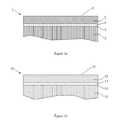
Figure 1 :Figure 1 illustrates- a) the different layers covering the polymer carrier object, and
- b) the different layers covering the substrate.
Figure 2 :Figure 2 schematically shows the UV based 2-step imprint process.
Figure 3 :Figure 3 displays AFM images of the substrate resist surfaces after performed imprints applying the UV-based 2-step imprint process. Stamps with various pattern sizes and the different IPS and substrate resist formulations have been applied.
- Anti-adhesion or adhesion at the interface between two different materials is strongly associated with the term surface energy or interface energy. The surface energy of a non-cured resist can be reduced significantly by the introduction of certain compounds e.g. fluoro-surfacants or siloxanes. Fluoro-surfactants phase segregates into a fluoro-surfactant poor and a fluoro-surfactant rich phase and the fluoro-surfactant rich phase is predominantly located close to the surface of the resist. After curing, the surfaces of fluoro-surfactant containing resists are characterized by low surface energies of 20 mJ/m2 or lower, and large contact angles observed with different organic and inorganic solvents. Polysiloxane comprising materials are also characterized by relatively low surface energies.
- Table 1 shows typical contact angles with water, 1,5-pentanediol, diiodomethane and ethylene glycol. Water contact angles higher than 100° could be observed for formulations after curing. Additionally, when the surface energy is divided into polar forces and dispersion forces, according to the model of Owens and Wendt, the surface energy γ of the IPS is strongly dominated by the dispersion contribution γd whereas the polar contribution γp is very low due to the non-polarity of the fluoro-surfactants.
- Table 2 presents some parameters which are important for the characterization of different surfaces or interfaces of the stamp/ IPS, e.g. γ, γd γp, WA, γ1,2. The different parameters have been calculated from contact angles measurements (table 1). As expected, the interfaces are characterized by low work of adhesions, WA, of approx. 30 mJ/m2 and low interface energies, γ1,2 of almost 0 mJ/m2 up to below 1 mJ/ m2. A low work of adhesion is very advantageous when a joint should exhibit low adhesion strength so that demolding can be performed easily. Low interface energies are found when the two surfaces establishing an interface are chemically very similar e.g. a joint consisting of two completely similar materials exhibits an interface energy of 0 mJ/m2.
- Formulations containing mixtures of different mono- or multi-functionalized monomers and/ or oligomers, which after curing exhibits high degrees of crosslinking and low solubility, are applied as imprint materials. The acrylate-based resists are characterized by high reactivity and polymerize rapidly in the presence of photogenerated free radicals, in the absence of oxygen at ambient temperature. Acrylates are for many reasons attractive material, but generally suffer from drawbacks such as high oxygen sensitivity and large shrinkage upon polymerization. Cationic induced polymerization of epoxides and vinyl ethers is comparatively slow, but offers several advantages such as good mechanical properties of the resist, low shrinkage, and an oxygen insensitive process. The present innovation describes how material properties from different polymers may be combined by blending proper ratios of interpenetrating polymer networks (IPNs) forming a hybrid polymer system comprising for example both acrylates and epoxides epoxides [Vabrik et al]. The synthesis of IPNs can be achieved by photoinitiated polymerization of monomers, which polymerize through different mechanisms, typically photoinitiated free radial mechanism and photoinitiated cationic mechanism.
- The developed IPS resist may be either a pure acrylate-based resist or a hybrid resist comprising both acrylates and epoxides. A high reactivity of the epoxy functionality is essential and obtained by the use of cyclic epoxides with a high intrinsic ring strain, such as the biscycloaliphatic epoxide with the following structure:

- Ring strains destabilize molecules due to a non-favourable high-energy spatial orientation of its atoms leading to a high curing rate and hereby circumvent the need of an additional thermal curing step. In spite of the high epoxide reactivity, acrylate-and epoxy-based hybrid resists are generally characterized by a fast curing of the acrylate monomers leading to a close to full conversion of the acrylates and lower conversions of the epoxides. A high conversion of the acrylates is essential if the substrate resist is acrylate based, as remaining acrylates present close to the surface of the IPS resist may participate in the polymerization process of the substrate resist leading to formation of covalent bonds between the IPS resist and the substrate resist.
- Proper selection of both the photoinitiators and radiation wavelengths enables a sequential build-up of a hybrid IPNs [Decker], [Decker, Decker]. This refinement of the hybrid polymerization allows the synthesis of a highly cross-linked acrylate network, prior to the initiation of the epoxy network synthesis. This is achieved by exposing the non-cured IPS formulation to filtered radiation (wavelength >350 nm), absorbed solely by the free radical photoinitiator e.g. 2,4,6-trimethylbenzoylphenylphosphinate, but not by the cationic photoinitiator. In the second step the sample is exposed to unfiltered photon based radiation, which is absorbed by the cationic photoinitiator e.g. triarylsulfonium hexafluorophosphate, thus initiating polymerization of the epoxy monomers within the existing acrylate polymer network forming the IPNs. The sequential polymerization is here presented as a promising technique for the improvement of material properties such as reduced polymer shrinkage, due to the low shrinkage of the epoxides, and higher imprint fidelity etc.
- An anti-sticking treatment of the IPS resist results in a low surface energy, which facilitates the release of the IPS resist and the substrate resist. In order to avoid surface treatment of the cured IPS resist it is advantageous if certain fluoro-surfactants or siloxanes are added to the mold material before curing. Especially, hydrophobic fluoro-surfactants molecule can be tailor-made to diffuse to the surface of the mold resist forming an anti-sticking layer. A common problem associated with this technique is that many fluoro-surfactants are only weakly non-covalently bound to the bulk material, which due to contaminations of the template stamp are less applicable in many NIL processes. The present innovation overcomes these problems by employing new fluoro-surfactants developed and optimized for the IPS resist/substrate resist imprinting technique as well as techniques developed for an efficient covalent attachment of the fluoro-surfactants previously used in a noncovalent mode.
- Zonyl® FSO-100 is a fluorosurfactant, which consists of a perfluorinated alkyl chain block and an ethylene glycol block terminated with a free hydroxyl functionality. It is manufactured by DuPont and has the following structure:

- Zonyl® FSO-100 has previously been employed in NIL applications only as a non-covalently attached anti-sticking agent. The terminal hydroxyl group of the fluorosurfactant is proposed to participate in the cationic polymerisation of an epoxide or vinyl ether monomer functioning as a chain transfer agent according to the mechanism illustrated below:

- The zonyl® FSO-100 molecule can hence be covalently attached to highly reactive epoxides or vinyl ethers, but generally not to other types of monomers polymerizable at room temperature, such as acrylates. Another related fluoro-surfactant suitable for covalent linkage to the IPS resist is the acrylic ester of zonyl® FSO 100 with the following structure:

One class of molecules that have showed strong potential as efficient fluoro-surfactants with the ability to diffuse to the surface of the mold resist forming an anti-sticking layer, are perfluoropolyether (PFPE) based derivatives end terminated with one or several chemical functionalities, such as acrylates. For example, the PFPE backbone has been linked to the acrylates via linear or branched aliphatic urethane block copolymers chain and is manufactured, which has the following structure: Yp-X-CF2CF2O(CF2F2O)m(CF2O)nCF2CF2-X-Yp,
where X is an aliphatic urethane building block, Y is a (meth)acrylate and p equals one or two. The molecular weight of the PFPE part of the co-polymer is 1500-2000 g/mol and the ratio m/n is 1.5 to 2.5. - The substrate resist may be a purely acrylate based resist, or a hybrid resist of acrylates and vinyl ethers with material properties combined from the two types of polymers. A hybrid comprising acrylate and vinyl ether will consist of both a copolymerized acrylate and vinyl ether network formed upon radical polymerization and a vinyl ether network formed upon cationic polymerization. The networks formed in the acrylate/vinyl ether hybrid will compared to the acrylate/epoxide hybrid be covalently linked to a much higher degree, due to the ability of the vinyl ether to undergo both free radical and cationic polymerization [Decker, Decker]. The substrate resist may contain various acryloxy-functionalized siloxanes. These are free radical polymerizable siloxanes typically prepared by silanization of hydroxyl-terminated polydimethylsiloxanes with various acryloxysilanes, such as 3-methacryloxypropyldimethylchlorosilane exemplified by the scheme below:

US Pat. No. 4675346 ) and a few acryloxy-functionalized siloxanes are also commercially available. Functionalized siloxanes may also be synthesised utilizing a transition-metal catalyzed hydrosilation of a hydrogen-terminated polydimethylsiloxanes and an olefin (e.g.US Pat. No. 6,828,404 B2 ) In order to minimize the interface energy, the functionalized polydimethylsiloxanes are likely to diffuse to the surface/ interface of the substrate resist and the IPS resist. Decreased work of adhesion and low concentration of reactive acrylates close to the surface functionalities are believed to aid the demolding process. A similar decrease in work of adhesion may also be achieved by the addition of other acryloxysilanes to the non-cured substrate resist, e.g. methacryloxypropyltris(trimethylsiloxy)silane with the following structure:
- The addition of silanes to the non-cured substrate resist will also improve the etch resistivity of the substrate resist.
- One of the primary objectives of this invention was to ease the demolding process by adjusting the surface energy of both the IPS resist and substrate resist and minimize the chemical interactions in the interface of the IPS and substrate resist. Consequently, the imprint may also be successful if a formulation originally designed as a substrate resist is employed as an IPS resist together with a substrate resist based upon a formulation originally designed as an IPS resist. However, only the IPS resist formulation may contain fluoro-surfactants while both the substrate resist and the IPS may contain functionalized siloxanes.
- An acrylic ester of Zonyl® FSO 100 was prepared from hydroxyl chain terminated fluorinated Zonyl® FSO 100 (Mw ∼725 g/mol, with (CF2CF2)x, n-4 and (CH2CH2O)y, n-8 from19F and1H NMR analysis) [Perrier et al]. To a solution of Zonyl® FSO 100 (5.0 grams, 6.9 mmol) and acryloyl chloride (0.75 grams, 8.3 mmol) in 30 mL of dichloromethane in was added triethylamine (0.3 mL) and the mixture was stirred for 4 h at 0 °C and then heated to ambient temperature and stirred for another 12 h. To the reaction was added 50 mL of ethyl acetate and the mixture was extracted twice with 30 mL of a saturated aqueous solution of NaHCO3 The organic layer was dried over MgSO4 and concentrated under reduced pressure to give the acrylic Zonyl® FSO 100 ester as a yellow oil (yield =90%).1H NMR (400 MHz, CDCl3): δ 6.43 ppm (1H, dd, CH2=CH-), 6.15 ppm (1H, dd, CH2=CH-), 5.83 ppm (1H, dd, CH2=CH-), 4.31 ppm (2H, m, -COO-CH2-), 3.6-3.8 ppm (32H, m, O-CH2-CH2-O), 2.43 ppm (2H, m, CH2-CF2-).
- The substrate resist may be a purely acrylate based resist, or a hybrid resist, with material properties combined from the two types of polymers, comprising acrylates and vinyl ethers, or acrylates and epoxides.
- Composition 1 (referred to as "IPS50") is a purely acrylate-based IPS formulation containing approximately 0.25% by weight of the fluoro-surfactant Y-X-CF2CF2O(CF2F2O)m(CF2O)nCF2CF2-X-Y, where X is a short linear urethane block copolymers chain and Y is a methacrylate group.
- Composition 2 (referred to as "IPS70/95") is an acrylate/epoxide-hybrid IPS formulation containing approximately 1% of Zonyl® FSO 100 derivatives by weight.
- Composition 3 (referred to as "IPS105") is an acrylate/epoxide-hybrid IPS formulation containing approximately 1% by weight of the fluoro-surfactant Y2-X-CF2CF2O(CF2F2O)n,(CF2O)nCF2CF2-X-Y2, where X is a long branched urethane block copolymers chain and Y is an acrylate group.
- Composition 4 (referred to as "IPS110") is an acrylate/epoxide-hybrid IPS formulation containing approximately 0.8% by weight of the fluoro-surfactant Y2-X-CF2CF2O(CF2F2O)m(CF2O)nCF2CF2-X-Y2, where X is a long branched urethane block copolymers chain and Y is an acrylate group, 0.6% of the acrylic ester of Zonyl® FSO 100 by weight.
- Composition 5 (referred to as "IPS102") is a purely acrylate-based IPS formulation containing approximately 1% by weight of the fluoro-surfactant Y2-X-CF2CF2O(CF2F2O)n,(CF2O)nCF2CF2-X-Y2, where X is a long branched urethane block copolymers chain and Y is an acrylate group.
- Substrate resist 1 (referred to as "SR20/47") is a purely acrylate-based substrate resist formulation without functionalized siloxanes.
- Substrate resist 2 compositions (referred to as "SR02") are purely acrylate-based substrates resist formulations containing functionalized siloxanes.
- Substrate resist 3 compositions (referred to as "SR35") are purely acrylate-based substrates resist formulations containing functionalized siloxanes.
- The two
material assemblies figures 1 a and 1 b, respectively, can be regarded as the essential prerequisite to succeed the two-step process illustrated infigure 2 . Here, the first step is illustrated infigs. 2a-2c and the second step infigs. 2d-2f . Infig. 2a the stamp ortemplate 10, composed of materials such as silicon, quartz, nickel or other metals, an alloy or possibly a polymer material, has a patterned surface 9, comprising ribs, grooves, protrusions or recesses, having heights and widths in the order of micrometers or nanometers. The template surface 9 is normally, but not exclusively, equipped with ananti-adhesion layer 8. Thetemplate 10 is placed with the surface of theanti-adhesion layer 8 contacting a surface 6 of thespecimen 1. A pressure of 1-40 bars is applied pressing thetemplate 10 and thespecimen 1 together. Resist 5 will fill the cavities of the template surface 9 and in order to minimize the interface energy of the interface between thetemplate anti-sticking layer 8 and the resist surface 6, fluoro-surfactants will predominately assemble close to the surface 6. - The sandwich arrangement - comprising a
template 10 equipped with ananti-sticking layer 8, apolymer carrier object 2, and photo-polymerizable resist 5 and possibly an adhesion promoter 4 - is irradiated with photons either through the backside of thetemplate 10 or through thepolymer carrier object 2 as displayed infig 2b ). In the first case the template has to be transparent, whereas in the second case the polymer carrier object has to fulfill this requirement. - Curing produces a solidified, low-surface-energy replica, having a pattern inversed to that of the original template. The
template 10 is separated or demolded from theflexible polymer replica 11 leaving a relief image on thesurface 13 of the solidifiedpolymer film 12, coated on thepolymer carrier object 2 as displayed inFig 2c . After demolding neither plastic deformations of patterns of thesurface 13 can be observed nor resist rip-off, e.g. residuals of resist 12 ontemplate 10. Theflexible polymer replica 11 herein is referred to as an intermediate polymer stamp (IPS).
In the second step of the two-step process, the pattern ofsurface 13 onIPS 11 is transferred to a target substrate as illustrated inFigs 2d) - 2f ). Here,surface 13 will be placed in contact withsurface 19 ofobject 14 comprising asubstrate 15 withsurface 16 covered by a thinmoldable layer 18 of a non-cured photo curable resist. A thinorganic layer 17 acting as an adhesion promoter might be placed in-between thesubstrate surface 16 and the resist 18.
As illustrated infig. 2e with the help of an applied pressure lying between 1 to 40 bars theIPS 11 andobject 14 will be forced together and cured with photon radiation. After demolding an inversion of the pattern on thesurface 13 of theIPS 11 has been formed in thesurface 22 of thelayer 21, as shown infig. 2f . - Several IPS and substrate resist formulations have been evaluated, fulfilling necessary requirements as materials for an improved imprint process, showing high replication fidelity, and which are industrially easy and suitable to employ. The different formulations may be applied within the 2-step process - schematically described in
figure 2 - without further anti-sticking treatment of the IPS surface (13 infigure 2c or 2d ), and thus avoids the need of external processes, such a plasma treatment, and/ or a coating with an additional thin film.
Five Selected examples of Ni stamps or templates displaying patterns as small as sub 100 nm range were covered by a thin anti-sticking film - as described in Japanese patent no.3892460 in 2006 - Table 1 displays contact angles for water, 1,5-pentanediol, diiodomethane and ethylene glycol applied to different surfaces. All measurements were carried out with a Tracker instrument from Teclis. The studied surfaces may be divided into three different categories:
- 1)
Row 1 androw 2 display data for a hydrophobic anti-sticked Ni template or stamp (surface 8 offigure 2a ). - 2)
Row 3 to row 7 display contact angles of the different IPS resists IPS102, IPS105, IPS110, IPS50 and IPS70/95 prepared by spin-coating the different formulations onto silicon wafers, pretreated with adhesion promoters, such as 3-(trimethoxysilyl)propyl methacrylate. The resulting film thicknesses were measured to be 600-1200 nm. Due to the presence of fluoro-surfactants, the surfaces display a pronounced hydrophobicity after curing.
- 1)
Row 8 to row 10 display contact angles for the substrate resist SR35, SR02, and SR20/47, prepared by spin-coating onto silicon wafers, pretreated with adhesion promoters, such as 3-(trimethoxysilyl)propyl methacrylate. The resulting film thicknesses are approximately 70 nm for SR02; and 600 nm for SR35 and SR20/47. The contact angles observed for the surfaces of the cured non-fluorinated substrate resists (rows 8-10) are significantly lower than those observed for the surfaces of the fluorinated IPS resists (rows 3-7).
With the help of the contact angles displayed in Table 1 the surface energies, together with their dispersion and polar contributions have been calculated utilizing the model of Owens, Wendt, Rabel and Kaelble. The different values are displayed in table 2columns Group 1 displays parameters characterizing the surfaces of the original Ni template, several cured-IPS resist compositions, and their interfaces (corresponding tosurfaces 8 offigure 2a and the surfaces 6 offigures 1 a and 2a after curing). The patterned Ni stamp surface is characterized by low surface energy dominated by the dispersion contribution γd.- The parameters displayed in
groups 2 to 5 stand for the interfaces of several IPS resist compositions and several substrate resist compositions. Each group represents the interfaces of one I PS resist to one or two substrates resists. The values represents the surfaces and interfaces between thesurface 13 offigures 2c and 2d and thesurface 19 offigures 1b and2d after curing. The calculated surface energies of the substrate resists are significantly larger than those of the surfactant containing IPS resists. - A 1,5 µm thick film of the IPS resists IPS70/95 was spin-coated onto a polycarbonate film having a thickness of 125 µm. A 2-step imprint process was carried out according to
figure 2 . The anti-sticking treatedNi stamp 1 was pressed against the polymer film for 60 sec with a pressure of 30 bars, the resist was cured with photon radiation for 90 sec as illustrated infigure 2b . During the exposure time the applied pressure was kept at 30 bars. Afterwards, the Ni stamp was separated from the cured IPS. The IPS comprising a polycarbonate film equipped with a completely cured IPS resist was applied in the second imprint process (figure 2d ). A SR02 substrate resist was spin-coated to a thickness of 50 nm onto a silicon wafer, pretreated with an 3-(trimethoxysilyl)propyl acrylate employed as an adhesion promoter for improved adhesion. The second imprint was performed as described above with a photon radiation time of 30 sec (figure 2e ). After demolding, the cured substrate resist was examined by AFM.Figure 3a displays an image of the substrate resist surface (surface 22 infigure 2f ) with dimensions of the applied Ni stamp pattern given in the caption offigure 3a . - An imprint with
Ni Stamp 2 was performed according to the description of Example 1 using a 1 µm thick SR20/47 film as substrate resist in the second imprint step and - in the second imprint step - with a photon radiation time of 60 sec.Figure 3b displays an image of the substrate resist surface with dimensions of the applied Ni stamp pattern given in the caption offigure 3b . - An imprint with
Ni Stamp 3 was performed according to the description of Example 1. However, the applied substrate resist (SR02) was 70 nm thick.Figure 3c displays an image of the substrate resist surface with dimensions of the applied Ni stamp pattern given in the caption offigure 3c . - An imprint with
Ni Stamp 3 was performed according to the description of Example 3 using a 1 µm thick IPS110 film as an IPS resist in the first imprint step.Figure 3d displays an image of the substrate resist surface with dimensions of the applied Ni stamp pattern given in the caption offigure 3d . - An imprint with
Ni Stamp 1 was performed according to the description of Example 1 using a 1.5 µm thick IPS105 film as an IPS resist in the first imprint step.Figure 3e displays an image of the substrate resist surface with dimensions of the applied Ni stamp pattern given in the caption offigure 3e . - An imprint with
Ni Stamp 4 exhibiting a smaller structure sizes, was performed according to the description of Example 5.Figure 3f displays an image of the substrate resist surface with dimensions of the applied Ni stamp pattern given in the caption offigure 3f . - An imprint with Ni Stamp 5, exhibiting a larger pattern, was performed according to the description of Example 1 using a 1.5 µm thick IPS50 film as IPS in the first imprint step and a 1 µm thick SR20/47 film as substrate resist in the second imprint step and an with a photon radiation time of 60 sec in both imprint steps.
Figure 3g displays an image of the substrate resist surface with dimensions of the applied Ni stamp pattern given in the caption offigure 3g .Table 1: water [°] 1,5-pentane diol [°] Diiodomethane [°] Ethylene Glycol [°] 1 Ni stamp patterned 107,6 87,5 92,5 - 2 Ni stamp non-patterned 106,3 81,4 87,7 - 3 IPS102 104,2 86,1 79,0 - 4 IPS105 105,1 86,5 86,2 - 5 IPS110 105,4 83,5 89,7 - 6 IPS50 100,7 - 78,8 88,1 7 IPS70/95 100,2 - - - 8 SR35 82,0 67,4 72,1 - 9 SR02 85,3 57,0 57,6 - 10 SR20/47 79,1 54,3 47,1 - Table 2: Column → Column 1: Template Column 2: Surface energy of the template Column 3: Replica Column 4: Surface energy of the replica Column 5: Interface parameters Group ↓ γ
[mJ/m2]γd
[mJ/m2]γp
[mJ/m2]γ
[mJ/m2]γd
[mJ/m2]γp
[mJ/m2]WA
[mJ/m2]γ1,2
[mJ/m2]Group 1Ni stamp patterned 13,14 11,37 1,77 IPS102 19,18 18,03 1,15 31,50 0,83 IPS105 16,09 14,44 1,65 29,04 0,19 IPS110 14,77 12,82 1,95 27,86 0,05 Group 2IPS102 19,18 18,03 1,15 SR35 29,30 21,69 7,61 45,47 3,01 SR02 33,69 29,95 3,74 50,63 2,25 Group 3IPS105 16,09 14,44 1,65 SR35 29,30 21,69 7,61 42,48 2,91 SR02 33,69 29,95 3,74 46,56 3,22 Group 4IPS110 14,77 12,82 1,95 SR35 29,30 21,69 7,61 41,10 3,01 SR02 33,69 29,95 3,74 44,95 3,87 Group 5 IPS15 20,15 18,13 2,02 SR20/47 36,25 31,64 4,61 54,00 2,40 - [Adamson, Gast]A. W Adamson and A.P. Gast "Physical Chemistry of Surfaces", John Wiley & Sons, Inc., New York, Sixth Edition, 1997.
- [Decker]C. Decker, "UV-radiation curing chemistry", Pigment & Resin Technology, Vol 30(5), 2001, pp 278-286.
- [Decker, Decker]C. Decker, D. Decker, "Photoinitiated polymerization of vinyl ether and acrylate monomer mixtures", J.M.S.-Pure Appl. Chem., Vol A34(4), 1997, pp 605-625.
- [Hiemenz, Rajagopalan]P.C. Hiemenz and R. Rajagopalan, "Principles of Colloid and Surface Chemistry", Marcel Dekker, Inc., New York, Third Edition, 1997.
- [Perrier et al]S. Perrier, S. G. Jackson, D.M. Haddleton, B. Ameduri, B. Boutevin, Tetrahedron, Vol 58, 2002, pp 4053-4059;S. Perrier, S. G. Jackson, D.M. Haddleton, B. Ameduri, B. Boutevin, macromolecules, Vol 36, 2003, pp 9042-9047.
- [Pocius]A. V. Pocius "Adhesion and Adhesive Technology", Hanser Publishers, Munich, Second Edition, 2002.
- [Vabrik el al]R. Vabrik, I. Czajlik, G. Tury, I. Rusznak, A. Ille, A. Vig, "A study of epoxy resin - acrylated polyurethane semi-interpenetrating polymer networks". Journal of applied polymer science, Vol 68, 1998, pp 111-119.


Claims (19)
- A process for providing a photocurable IPS material, applicable in a 2-step imprint method for the transferring of a pattern from an anti-sticking stamp to an I PS and the use of the patterned IPS as a template for the transferring of the pattern onto the surface of a substrate resist, comprising photoinitiators or catalysts with the ability to initiate polymerization, polymerizable mono- or multifunctional monomers and fluoro-surfactants completely or partly terminated by functional groups with the ability to covalently bind to the resist under curing.
- The process of claim 1, wherein the concentration of perfluorinated fluoro-surfactants ranges from 0% to 30% and the said fluoro-surfactants are surface-active, implying that the concentration of fluoro-surfactants is significantly higher in proximity of the surface /interface region and that the material ischaracterized by low work of adhesion and not negligible interface energy.
- The process of claim 1 and 2, wherein the non-cured IPS material contains polymerizable mono- or multifunctional acrylate-based monomers and at least one free radical photoinitiator.
- The process of claim 1 and 2, wherein the non-cured IPS resist formulation is a hybrid, comprising polymerizable mono- or multifunctional acrylate monomers, polymerizable mono- or multifunctional epoxides and at least one free radical photoinitiators as well as at least one cationic photoinitiator, which upon photon-radiation forms a hybrid material comprising interpenetrating networks of polymerized acrylates and epoxides.
- The process of claim 1 and 2, wherein the non-cured IPS resist formulation is a hybrid, comprising polymerizable mono- or multifunctional acrylate monomers, polymerizable mono- or multifunctional vinyl ethers and at least one free radical photoinitiators as well as at least one cationic photoinitiator, which upon photon-radiation forms a hybrid material comprising interpenetrating networks of both copolymerized acrylates and vinyl ethers as well as vinyl ethers.
- The process of claim 1 and 2, wherein the fluoro-surfactants is a PFPE copolymers with the structure Yp-X-CF2CF2O(CF2F2O)m(CF2O)nCF2CF2-X-Yp, where X is an aliphatic urethane block, Y is an acrylate or a methacrylate, m and n are integers, and p equals 1, 2 or 3, with a molecular weight of the PFPE part of the co-polymer of 800-2500 g/mol.
- The process of claim 1, 2, 4, 5, and 6, wherein X is an aliphatic copolymer block and the material is a hybrid comprising interpenetrating networks of acrylates and epoxides, or acrylates and vinyl ethers.
- The process of claim 1 and 2, wherein the said fluoro-surfactant is an acrylic ester of zonyl® FSO 100 with the following structure:

- The process of claim 1 and 2, wherein the said fluoro-surfactant is zonyl® FSO 100 or derivatives of zonyl® FSO 100 covalently linked to the cured material.
- The process of claims 1-9, wherein the work of adhesion of the IPS/ substrate resist interface is smaller than 65 mJ/m2 (preferably smaller than 30 mJ/m2) and the interface energy of the polymer mold/ replica interface is larger than 1 mJ/m2 (preferably larger than 4 mJ/m2).
- The process of claims in 1 -10, wherein said molecules are used in Nano Imprint Lithography applications.
- A process for providing a photocurable IPS material, applicable in a 2-step imprint method for the transferring of a pattern from a non-surface treated stamp to an I PS and the use of the patterned I PS as a template for the transferring of the pattern onto the surface of a substrate resist, comprising photoinitiators or catalysts with the ability to initiate polymerization, polymerizable mono- or multifunctional acrylates, epoxides or vinyls and siloxanes completely or partly terminated by acryloyl, epoxy or vinyl functionalities with the ability to covalently bind to the resist under curing.
- The process of claim 12, wherein the weight concentration of silicon containing molecules is higher than 40% and the work of adhesion of the IPS/ substrate resist interface is smaller than 65 mJ/m2 (preferably smaller than 30 mJ/m2) and the interface energy of the polymer mold/ replica interface is larger than 1 mJ/m2 (preferably larger than 4 mJ/m2).
- A method of providing photcurable substrate resist, applicable in a 2-step imprint method for the transferring of a pattern from a stamp to an I PS and the use of the patterned IPS as a template for the transferring of the pattern onto the surface of a substrate resist, comprising photoinitiators or catalysts with the ability to initiate polymerization, polymerizable mono- or multifunctional monomers and derivatives of siloxanes and polydimethylsiloxanes completely or partly terminated by functional groups with the ability to covalently bind to the resist under curing.
- The method of claim 14, wherein the non-cured substrate resist formulation contains polymerizable mono- or multifunctional (meth)acrylate-based monomers and at least one free radical photoinitiator.
- The method of claim 14, wherein the non-cured substrate resist formulation is a hybrid, comprising polymerizable mono- or multifunctional (meth)acrylate monomers, polymerizable mono- or multifunctional epoxides and at least one free radical photoinitiators as well as at least one cationic photoinitiator, which upon photon-radiation formes a hybrid material comprising interpenetrating networks of polymerized (meth)acrylates and epoxides.
- The method of claim 14, wherein the non-cured substrate resist formulation is a hybrid, comprising polymerizable mono- or multifunctional (meth)acrylate monomers, polymerizable mono- or multifunctional vinyl ethers and at least one free radical photoinitiators as well as at least one cationic photoinitiator, which upon photon-radiation forms a hybrid material comprising interpenetrating networks of both copolymerized (meth)acrylates and vinyl ethers as well as vinyl ethers.
- The method of claim 14, wherein the non-cured substrate resist formulation comprises derivatives of polydimethylsiloxanes, which upon curing will be covalently linked to (meth)acrylate, epoxide or vinyl ether networks in a hybrid material, showing the following structure:

- The method of claims in 14 -18, wherein said substrate resist are used in Nano Imprint Lithography applications.


Priority Applications (9)
| Application Number | Priority Date | Filing Date | Title |
|---|---|---|---|
| EP08172342.1AEP2199855B1 (en) | 2008-12-19 | 2008-12-19 | Methods and processes for modifying polymer material surface interactions |
| SG200908085-4ASG162674A1 (en) | 2008-12-19 | 2009-12-04 | Methods and processes for modifying polymer material surface interactions |
| US12/635,329US9063408B2 (en) | 2008-12-19 | 2009-12-10 | Methods and processes for modifying polymer material surface interactions |
| JP2009283148AJP5725465B2 (en) | 2008-12-19 | 2009-12-14 | Methods and processes for altering polymeric material surface interactions |
| TW098143041ATWI515510B (en) | 2008-12-19 | 2009-12-16 | Methods and processes for modifying polymer material surface interactions |
| CN200910261311.2ACN101872115B (en) | 2008-12-19 | 2009-12-17 | The Method and process of modifying polymer material surface interactions |
| KR1020090126769AKR101767179B1 (en) | 2008-12-19 | 2009-12-18 | Methods and processes for modifying polymer material surface interactions |
| HK11104086.4AHK1149804B (en) | 2008-12-19 | 2011-04-21 | Methods and processes for modifying polymer material surface interactions |
| JP2015022431AJP5838002B2 (en) | 2008-12-19 | 2015-02-06 | Methods and processes for altering polymeric material surface interactions |
Applications Claiming Priority (1)
| Application Number | Priority Date | Filing Date | Title |
|---|---|---|---|
| EP08172342.1AEP2199855B1 (en) | 2008-12-19 | 2008-12-19 | Methods and processes for modifying polymer material surface interactions |
Publications (2)
| Publication Number | Publication Date |
|---|---|
| EP2199855A1true EP2199855A1 (en) | 2010-06-23 |
| EP2199855B1 EP2199855B1 (en) | 2016-07-20 |
Family
ID=40521956
Family Applications (1)
| Application Number | Title | Priority Date | Filing Date |
|---|---|---|---|
| EP08172342.1AActiveEP2199855B1 (en) | 2008-12-19 | 2008-12-19 | Methods and processes for modifying polymer material surface interactions |
Country Status (7)
| Country | Link |
|---|---|
| US (1) | US9063408B2 (en) |
| EP (1) | EP2199855B1 (en) |
| JP (2) | JP5725465B2 (en) |
| KR (1) | KR101767179B1 (en) |
| CN (1) | CN101872115B (en) |
| SG (1) | SG162674A1 (en) |
| TW (1) | TWI515510B (en) |
Cited By (2)
| Publication number | Priority date | Publication date | Assignee | Title |
|---|---|---|---|---|
| WO2012025316A1 (en)* | 2010-08-26 | 2012-03-01 | Asml Netherlands B.V. | Imprint lithography method and imprintable medium |
| WO2013118791A1 (en) | 2012-02-09 | 2013-08-15 | Canon Kabushiki Kaisha | Photocured product and method for producing the same |
Families Citing this family (30)
| Publication number | Priority date | Publication date | Assignee | Title |
|---|---|---|---|---|
| JP5321228B2 (en)* | 2009-04-28 | 2013-10-23 | Jsr株式会社 | Photocurable composition for nanoimprint lithography and nanoimprint method |
| KR101653626B1 (en)* | 2009-07-13 | 2016-09-02 | 주식회사 동진쎄미켐 | Photocurable fluoro resin composition and method for preparing of mold using the same |
| JP2013518740A (en)* | 2010-02-05 | 2013-05-23 | オブダカット・アーベー | Methods and processes for metal stamp replication for large area nanopatterns |
| KR101381489B1 (en)* | 2010-03-10 | 2014-04-04 | 아사히 가세이 이-매터리얼즈 가부시키가이샤 | Resin mold |
| CN103068556B (en)* | 2010-08-06 | 2015-07-22 | 综研化学株式会社 | Resin mold for nanoimprinting and manufacturing method thereof |
| JP5306404B2 (en)* | 2011-03-25 | 2013-10-02 | 株式会社東芝 | Pattern formation method |
| NL2010004A (en)* | 2012-01-13 | 2013-07-16 | Asml Netherlands Bv | Self-assemblable polymer and methods for use in lithography. |
| JP6090732B2 (en)* | 2012-05-14 | 2017-03-08 | 東洋合成工業株式会社 | Optical imprint method |
| US10126648B2 (en)* | 2012-05-25 | 2018-11-13 | Micro Resist Technology Gesellschaft Für Chemische Materialien Spezieller Protoresistsysteme Gmbh | Composition suitable for use as a release-optimized material for nanoimprint processes and uses thereof |
| JP6071255B2 (en)* | 2012-06-04 | 2017-02-01 | キヤノン株式会社 | Photocured material |
| WO2014041846A1 (en) | 2012-09-14 | 2014-03-20 | Pola Pharma Inc. | Use of surface free energy for differential evaluation of crystal, crystal evaluated on basis of surface free energy as index, and phrmaceutical composition prepared by containing the crystal |
| KR101332323B1 (en)* | 2013-04-01 | 2013-11-25 | 한국기계연구원 | Apparatus for manufacturing roll stamp, method for manufacturing roll stamp using the same and method for manufacturing replication stamp |
| US9981419B2 (en)* | 2013-06-19 | 2018-05-29 | Ev Group E. Thallner Gmbh | Embossing compound for embossing lithography |
| JP5985442B2 (en)* | 2013-07-26 | 2016-09-06 | 株式会社東芝 | Resist material and pattern forming method using the same |
| EP3074819B1 (en)* | 2013-11-29 | 2023-04-12 | EV Group E. Thallner GmbH | Mould with a mould pattern, and method for producing same |
| JP6371076B2 (en)* | 2014-02-24 | 2018-08-08 | 旭化成株式会社 | Method for producing film mold |
| US10754244B2 (en)* | 2016-03-31 | 2020-08-25 | Canon Kabushiki Kaisha | Pattern forming method as well as production methods for processed substrate, optical component, circuit board, electronic component and imprint mold |
| JP6754344B2 (en)* | 2017-09-26 | 2020-09-09 | 富士フイルム株式会社 | Composition for forming underlayer film for imprint, kit, laminate, method for manufacturing laminate, method for manufacturing cured product pattern, method for manufacturing circuit board |
| JP2018166222A (en)* | 2018-07-13 | 2018-10-25 | エーファウ・グループ・エー・タルナー・ゲーエムベーハー | Stamper having stamper structure and manufacturing method thereof |
| US11549020B2 (en) | 2019-09-23 | 2023-01-10 | Canon Kabushiki Kaisha | Curable composition for nano-fabrication |
| JP2023522499A (en)* | 2020-04-24 | 2023-05-31 | イルミナ ケンブリッジ リミテッド | flow cell |
| CN112731764A (en)* | 2020-12-29 | 2021-04-30 | 苏州理硕科技有限公司 | Negative photoresist composition and method for forming photoresist pattern |
| US11884977B2 (en) | 2021-03-12 | 2024-01-30 | Singular Genomics Systems, Inc. | Nanoarrays and methods of use thereof |
| EP4263868A4 (en) | 2021-03-12 | 2024-11-27 | Singular Genomics Systems, Inc. | NANOARRAYS AND METHODS OF USE THEREOF |
| WO2022232308A1 (en) | 2021-04-27 | 2022-11-03 | Singular Genomics Systems, Inc. | High density sequencing and multiplexed priming |
| WO2023034920A2 (en) | 2021-09-03 | 2023-03-09 | Singular Genomics Systems, Inc. | Amplification oligonucleotides |
| EP4422792A1 (en) | 2021-10-26 | 2024-09-04 | Singular Genomics Systems, Inc. | Multiplexed targeted amplification of polynucleotides |
| US20250188521A1 (en) | 2022-03-10 | 2025-06-12 | Singular Genomics Systems, Inc. | Nucleic acid delivery scaffolds |
| AU2024215695A1 (en) | 2023-02-01 | 2025-08-07 | Singular Genomics Systems, Inc. | Methods and devices for manipulating biological samples |
| TWI887123B (en)* | 2024-09-20 | 2025-06-11 | 華碩電腦股份有限公司 | Imprint ink and imprint method using the same |
Citations (10)
| Publication number | Priority date | Publication date | Assignee | Title |
|---|---|---|---|---|
| US4675346A (en) | 1983-06-20 | 1987-06-23 | Loctite Corporation | UV curable silicone rubber compositions |
| WO2003072625A1 (en)* | 2002-02-28 | 2003-09-04 | Luvantix Co., Ltd. | Photocurable resin composition for optical waveguide and optical waveguide made of the same |
| WO2004036302A1 (en)* | 2002-10-17 | 2004-04-29 | Zbd Displays Ltd. | Liquid crystal alignment layer |
| US20040110856A1 (en)* | 2002-12-04 | 2004-06-10 | Young Jung Gun | Polymer solution for nanoimprint lithography to reduce imprint temperature and pressure |
| US20040137734A1 (en)* | 1995-11-15 | 2004-07-15 | Princeton University | Compositions and processes for nanoimprinting |
| US6828404B2 (en) | 2000-10-20 | 2004-12-07 | Rensselaer Polytechnic Institute | Polymerizable siloxanes |
| JP3892460B2 (en) | 2002-06-20 | 2007-03-14 | オブデュキャット、アクチボラグ | Method for manufacturing a forming tool and storage medium formed using the forming tool |
| US20070272825A1 (en)* | 2004-01-23 | 2007-11-29 | Molecular Imprints, Inc. | Composition to Reduce Adhesion Between a Conformable Region and a Mold |
| US20080000373A1 (en)* | 2006-06-30 | 2008-01-03 | Maria Petrucci-Samija | Printing form precursor and process for preparing a stamp from the precursor |
| JP2008515059A (en) | 2004-09-24 | 2008-05-08 | スリーエム イノベイティブ プロパティズ カンパニー | Frequency control in closed loop control systems. |
Family Cites Families (62)
| Publication number | Priority date | Publication date | Assignee | Title |
|---|---|---|---|---|
| GB559072A (en) | 1940-08-03 | 1944-02-02 | Budd Edward G Mfg Co | A method of making stamping dies |
| US2305433A (en)* | 1940-09-11 | 1942-12-15 | Jesse B Hawley | Method and apparatus for molding articles of thermoplastic, thermosetting, or resinous materials |
| NL68070C (en) | 1947-01-17 | |||
| US2883372A (en)* | 1957-03-14 | 1959-04-21 | Du Pont | Copolymers of ethylene and dihydrodicyclopentadiene |
| US4211617A (en)* | 1975-02-24 | 1980-07-08 | Mca Disco-Vision, Inc. | Process for producing a stamper for videodisc purposes |
| US4477326A (en)* | 1983-06-20 | 1984-10-16 | Loctite Corporation | Polyphotoinitiators and compositions thereof |
| DD251847A1 (en) | 1986-07-31 | 1987-11-25 | Zeiss Jena Veb Carl | METHOD AND ARRANGEMENT FOR IMAGE COMPARISON |
| JPH0830106B2 (en) | 1989-06-24 | 1996-03-27 | 日本ゼオン株式会社 | Molding material |
| US5334424A (en)* | 1991-06-17 | 1994-08-02 | Nippon Zeon Co., Ltd. | Thermoplastic norbornene resin formed articles and sustrates for liquid crystal display |
| US5312794A (en)* | 1992-12-29 | 1994-05-17 | Shell Oil Company | Catalyst system for olefin polymerization |
| US5512131A (en)* | 1993-10-04 | 1996-04-30 | President And Fellows Of Harvard College | Formation of microstamped patterns on surfaces and derivative articles |
| AU6752496A (en) | 1995-07-28 | 1997-03-05 | Ely Michael Rabani | Pattern formation, replication, fabrication and devices thereby |
| US5772905A (en)* | 1995-11-15 | 1998-06-30 | Regents Of The University Of Minnesota | Nanoimprint lithography |
| JPH09330864A (en) | 1996-06-10 | 1997-12-22 | Ge Yokogawa Medical Syst Ltd | Method and mask for manufacturing composite piezoelectric material |
| JPH10330577A (en) | 1997-03-31 | 1998-12-15 | Mitsui Chem Inc | Cycloolefin resin molding and method for stamping character thereon |
| US6334960B1 (en)* | 1999-03-11 | 2002-01-01 | Board Of Regents, The University Of Texas System | Step and flash imprint lithography |
| DE19920941A1 (en)* | 1999-05-07 | 2000-11-16 | Krauss Maffei Kunststofftech | Method for producing plastic parts with an embossed structure and device for carrying out the method |
| SE515607C2 (en) | 1999-12-10 | 2001-09-10 | Obducat Ab | Device and method for fabrication of structures |
| DE10009246A1 (en) | 2000-02-28 | 2001-08-30 | Mitsubishi Polyester Film Gmbh | White, biaxially oriented and UV-stabilized polyester film with cycloolefinocopolymer (COC), process for its production and its use |
| DE10011652A1 (en) | 2000-03-10 | 2001-09-13 | Mitsubishi Polyester Film Gmbh | Biaxially oriented polyester film with high whiteness, process for its production and its use |
| WO2001070489A1 (en) | 2000-03-16 | 2001-09-27 | Mitsubishi Polyester Film, Llc | White polyester film with cycloolefin copolymer |
| KR100694036B1 (en) | 2000-06-01 | 2007-03-12 | 삼성전자주식회사 | Discs with different groove and pit depths and manufacturing method |
| AU2001281021A1 (en) | 2000-08-01 | 2002-02-13 | The Deflex Corporation | Gas-vapor cleaning method and system therefor |
| JP4192414B2 (en) | 2000-09-14 | 2008-12-10 | 凸版印刷株式会社 | Lens sheet manufacturing method |
| EP1352295B1 (en)* | 2000-10-12 | 2015-12-23 | Board of Regents, The University of Texas System | Template for room temperature, low pressure micro- and nano-imprint lithography |
| US6705853B1 (en)* | 2000-10-20 | 2004-03-16 | Durakon Industries, Inc. | Six station rotary thermoforming machine |
| US6953332B1 (en)* | 2000-11-28 | 2005-10-11 | St. Jude Medical, Inc. | Mandrel for use in forming valved prostheses having polymer leaflets by dip coating |
| US6422528B1 (en)* | 2001-01-17 | 2002-07-23 | Sandia National Laboratories | Sacrificial plastic mold with electroplatable base |
| US6815739B2 (en)* | 2001-05-18 | 2004-11-09 | Corporation For National Research Initiatives | Radio frequency microelectromechanical systems (MEMS) devices on low-temperature co-fired ceramic (LTCC) substrates |
| US20030071016A1 (en) | 2001-10-11 | 2003-04-17 | Wu-Sheng Shih | Patterned structure reproduction using nonsticking mold |
| JP3749520B2 (en) | 2002-01-08 | 2006-03-01 | Tdk株式会社 | Manufacturing method of stamper for manufacturing information medium, stamper, and stamper intermediate with master |
| TWI258142B (en) | 2002-01-08 | 2006-07-11 | Tdk Corp | Manufacturing method of stamper for manufacturing data medium, the stamper, and the stamper spacer with template |
| EP1353229A1 (en)* | 2002-04-09 | 2003-10-15 | ASML Netherlands B.V. | Lithographic apparatus, device manufacturing method and device manufactured thereby |
| DE10217151A1 (en)* | 2002-04-17 | 2003-10-30 | Clariant Gmbh | Nanoimprint resist |
| EP1364663A1 (en)* | 2002-05-21 | 2003-11-26 | Commonwealth Scientific And Industrial Research Organisation | Ocular devices with functionalized surface with adhesive properties |
| US20030230817A1 (en)* | 2002-06-13 | 2003-12-18 | Agere Systems, Inc. | Mold for UV curable adhesive and method of use therefor |
| US20050146083A1 (en)* | 2002-06-20 | 2005-07-07 | Lennart Olsson | Method and device for transferring a pattern |
| WO2004013693A2 (en)* | 2002-08-01 | 2004-02-12 | Molecular Imprints, Inc. | Scatterometry alignment for imprint lithography |
| US20040032063A1 (en)* | 2002-08-16 | 2004-02-19 | Peter Walther | Process for shaping plate-shaped materials and an arrangement for carrying out the process |
| US7754131B2 (en) | 2002-08-27 | 2010-07-13 | Obducat Ab | Device for transferring a pattern to an object |
| DE10311855B4 (en)* | 2003-03-17 | 2005-04-28 | Infineon Technologies Ag | Arrangement for transferring information / structures to wafers using a stamp |
| JP4061220B2 (en)* | 2003-03-20 | 2008-03-12 | 株式会社日立製作所 | Nanoprint apparatus and fine structure transfer method |
| EP1620205A2 (en) | 2003-04-04 | 2006-02-01 | Tecan Trading AG | Elastomeric tools for fabricating of polymeric devices and uses thereof |
| US20050191419A1 (en)* | 2003-04-11 | 2005-09-01 | Helt James M. | Fabrication of nanostructures |
| TW568349U (en)* | 2003-05-02 | 2003-12-21 | Ind Tech Res Inst | Parallelism adjusting device for nano-transferring |
| US7150844B2 (en)* | 2003-10-16 | 2006-12-19 | Seagate Technology Llc | Dry passivation process for stamper/imprinter family making for patterned recording media |
| US20050084804A1 (en)* | 2003-10-16 | 2005-04-21 | Molecular Imprints, Inc. | Low surface energy templates |
| US6939664B2 (en)* | 2003-10-24 | 2005-09-06 | International Business Machines Corporation | Low-activation energy silicon-containing resist system |
| GB0325748D0 (en) | 2003-11-05 | 2003-12-10 | Koninkl Philips Electronics Nv | A method of forming a patterned layer on a substrate |
| DE60336322D1 (en) | 2003-11-21 | 2011-04-21 | Obducat Ab | Nanoimprint lithography in multilayer systems |
| EP1538482B1 (en) | 2003-12-05 | 2016-02-17 | Obducat AB | Device and method for large area lithography |
| EP3242318A1 (en) | 2003-12-19 | 2017-11-08 | The University of North Carolina at Chapel Hill | Monodisperse micro-structure or nano-structure product |
| DE102004005247A1 (en)* | 2004-01-28 | 2005-09-01 | Infineon Technologies Ag | Imprint-lithographic process for manufacturing e.g. MOSFET, involves structuring polymerized gate dielectric layer by imprint stamp that is used to form hole on layer, and etching base of hole till preset thickness of layer is reached |
| EP1594001B1 (en) | 2004-05-07 | 2015-12-30 | Obducat AB | Device and method for imprint lithography |
| JP2008500914A (en) | 2004-05-28 | 2008-01-17 | オブデュキャット、アクチボラグ | Modified metal mold used for imprinting process |
| US7163888B2 (en)* | 2004-11-22 | 2007-01-16 | Motorola, Inc. | Direct imprinting of etch barriers using step and flash imprint lithography |
| CN101151555A (en)* | 2004-12-30 | 2008-03-26 | 3M创新有限公司 | Internal components of optical device comprising hardcoat |
| JP5276436B2 (en)* | 2005-06-10 | 2013-08-28 | オブデュキャット、アクチボラグ | Pattern duplication with intermediate stamp |
| US7878791B2 (en)* | 2005-11-04 | 2011-02-01 | Asml Netherlands B.V. | Imprint lithography |
| US20080047930A1 (en)* | 2006-08-23 | 2008-02-28 | Graciela Beatriz Blanchet | Method to form a pattern of functional material on a substrate |
| US20080110557A1 (en)* | 2006-11-15 | 2008-05-15 | Molecular Imprints, Inc. | Methods and Compositions for Providing Preferential Adhesion and Release of Adjacent Surfaces |
| EP2199854B1 (en)* | 2008-12-19 | 2015-12-16 | Obducat AB | Hybrid polymer mold for nano-imprinting and method for making the same |
- 2008
- 2008-12-19EPEP08172342.1Apatent/EP2199855B1/enactiveActive
- 2009
- 2009-12-04SGSG200908085-4Apatent/SG162674A1/enunknown
- 2009-12-10USUS12/635,329patent/US9063408B2/enactiveActive
- 2009-12-14JPJP2009283148Apatent/JP5725465B2/enactiveActive
- 2009-12-16TWTW098143041Apatent/TWI515510B/enactive
- 2009-12-17CNCN200910261311.2Apatent/CN101872115B/enactiveActive
- 2009-12-18KRKR1020090126769Apatent/KR101767179B1/enactiveActive
- 2015
- 2015-02-06JPJP2015022431Apatent/JP5838002B2/enactiveActive
Patent Citations (10)
| Publication number | Priority date | Publication date | Assignee | Title |
|---|---|---|---|---|
| US4675346A (en) | 1983-06-20 | 1987-06-23 | Loctite Corporation | UV curable silicone rubber compositions |
| US20040137734A1 (en)* | 1995-11-15 | 2004-07-15 | Princeton University | Compositions and processes for nanoimprinting |
| US6828404B2 (en) | 2000-10-20 | 2004-12-07 | Rensselaer Polytechnic Institute | Polymerizable siloxanes |
| WO2003072625A1 (en)* | 2002-02-28 | 2003-09-04 | Luvantix Co., Ltd. | Photocurable resin composition for optical waveguide and optical waveguide made of the same |
| JP3892460B2 (en) | 2002-06-20 | 2007-03-14 | オブデュキャット、アクチボラグ | Method for manufacturing a forming tool and storage medium formed using the forming tool |
| WO2004036302A1 (en)* | 2002-10-17 | 2004-04-29 | Zbd Displays Ltd. | Liquid crystal alignment layer |
| US20040110856A1 (en)* | 2002-12-04 | 2004-06-10 | Young Jung Gun | Polymer solution for nanoimprint lithography to reduce imprint temperature and pressure |
| US20070272825A1 (en)* | 2004-01-23 | 2007-11-29 | Molecular Imprints, Inc. | Composition to Reduce Adhesion Between a Conformable Region and a Mold |
| JP2008515059A (en) | 2004-09-24 | 2008-05-08 | スリーエム イノベイティブ プロパティズ カンパニー | Frequency control in closed loop control systems. |
| US20080000373A1 (en)* | 2006-06-30 | 2008-01-03 | Maria Petrucci-Samija | Printing form precursor and process for preparing a stamp from the precursor |
Non-Patent Citations (9)
| Title |
|---|
| A. V. POCIUS: "Adhesion and Adhesive Technology", 2002, HANSER PUBLISHERS |
| A.W. ADAMSON; A.P. GAST: "Physical Chemistry of Surfaces", 1997, JOHN WILEY & SONS, INC. |
| BARBERO D R ET AL: "HIGH RESOLUTION NANOIMPRINTING WITH A ROBUST AND REUSABLE POLYMER MOLD", ADVANCED FUNCTIONAL MATERIALS, WILEY VCH, WIENHEIM, DE, vol. 17, no. 14, 24 September 2007 (2007-09-24), pages 2419 - 2425, XP001506358, ISSN: 1616-301X* |
| C. DECKER: "UV-radiation curing chemistry", PIGMENT & RESIN TECHNOLOGY, vol. 30, no. 5, 2001, pages 278 - 286 |
| C. DECKER; D. DECKER: "Photoinitiated polymerization of vinyl etherand acrylate monomer mixtures", J.M.S.-PURE APPL. CHEM., vol. A34, no. 4, 1997, pages 605 - 625 |
| P.C. HIEMENZ; R. RAJAGOPALAN: "Principles of Colloidand Surface Chemistry", 1997, MARCEL DEKKER, INC. |
| R. VABRIK ET AL.: "A studyof epoxy resin - acrylated polyurethane semi-interpenetrating polymernetworks", JOURNAL OF APPLIED POLYMER SCIENCE, vol. 68, 1998, pages 111 - 119 |
| S. PERRIER ET AL., MACROMOLECULES, vol. 36, 2003, pages 9042 - 9047 |
| S. PERRIER, S. G. ET AL., BOUTEVIN, TETRAHEDRON, vol. 58, 2002, pages 4053 - 4059 |
Cited By (6)
| Publication number | Priority date | Publication date | Assignee | Title |
|---|---|---|---|---|
| WO2012025316A1 (en)* | 2010-08-26 | 2012-03-01 | Asml Netherlands B.V. | Imprint lithography method and imprintable medium |
| US9372399B2 (en) | 2010-08-26 | 2016-06-21 | Asml Netherlands B.V. | Imprint lithography method and imprintable medium |
| WO2013118791A1 (en) | 2012-02-09 | 2013-08-15 | Canon Kabushiki Kaisha | Photocured product and method for producing the same |
| EP2791965A4 (en)* | 2012-02-09 | 2015-08-19 | Canon Kk | Photocured product and method for producing the same |
| US9704710B2 (en) | 2012-02-09 | 2017-07-11 | Canon Kabushiki Kaisha | Photocured product and method for producing the same |
| US10535519B2 (en) | 2012-02-09 | 2020-01-14 | Canon Kabushiki Kaisha | Photocurable composition, method for forming a pattern, and method for producing a photocured product |
Also Published As
| Publication number | Publication date |
|---|---|
| US20100160478A1 (en) | 2010-06-24 |
| TWI515510B (en) | 2016-01-01 |
| JP5838002B2 (en) | 2015-12-24 |
| JP2010183064A (en) | 2010-08-19 |
| CN101872115A (en) | 2010-10-27 |
| HK1149804A1 (en) | 2011-10-14 |
| CN101872115B (en) | 2015-09-30 |
| KR101767179B1 (en) | 2017-08-10 |
| US9063408B2 (en) | 2015-06-23 |
| TW201027251A (en) | 2010-07-16 |
| JP5725465B2 (en) | 2015-05-27 |
| KR20100071925A (en) | 2010-06-29 |
| JP2015097293A (en) | 2015-05-21 |
| EP2199855B1 (en) | 2016-07-20 |
| SG162674A1 (en) | 2010-07-29 |
Similar Documents
| Publication | Publication Date | Title |
|---|---|---|
| EP2199855B1 (en) | Methods and processes for modifying polymer material surface interactions | |
| US8426025B2 (en) | Process and method for modifying polymer film surface interaction | |
| US8293354B2 (en) | UV curable silsesquioxane resins for nanoprint lithography | |
| EP1796851B1 (en) | Polymerization technique to attenuate oxygen inhibition of solidification of liquids | |
| CN101479662B (en) | Printing form precursor and method of making stamper from same | |
| US7452574B2 (en) | Method to reduce adhesion between a polymerizable layer and a substrate employing a fluorine-containing layer | |
| US9314963B2 (en) | Imprint product and method for producing the same | |
| WO2010064726A2 (en) | Curable composition for imprints, patterning method and pattern | |
| TW201038594A (en) | Curable composition for nanoimprint and cured product | |
| KR20120055242A (en) | Photocurable resin composition and method for preparing self-duplicable replica mold using same | |
| Min et al. | UV-curable nanoimprint resist with liquid volume-expanding monomers | |
| Du et al. | Modulus-and surface-energy-tunable thiol–ene for UV micromolding of coatings | |
| JP7663550B2 (en) | Photocurable resin composition for imprint mold, resin mold, pattern formation method using said resin mold, composite having said resin mold, method for manufacturing said composite, and method for manufacturing optical member | |
| JP2010206115A (en) | Photosensitive resin composition for optical nanoimprint lithography, method of forming pattern using the same, microstructure, and method of removing photocured body | |
| JP2011148117A (en) | Imprinting mold release agent | |
| HK1149804B (en) | Methods and processes for modifying polymer material surface interactions | |
| Du | UV curing and micromolding of polymer coatings | |
| Stacey et al. | Compositions for dark-field polymerization and method of using the same for imprint lithography processes |
Legal Events
| Date | Code | Title | Description |
|---|---|---|---|
| PUAI | Public reference made under article 153(3) epc to a published international application that has entered the european phase | Free format text:ORIGINAL CODE: 0009012 | |
| AK | Designated contracting states | Kind code of ref document:A1 Designated state(s):AT BE BG CH CY CZ DE DK EE ES FI FR GB GR HR HU IE IS IT LI LT LU LV MC MT NL NO PL PT RO SE SI SK TR | |
| AX | Request for extension of the european patent | Extension state:AL BA MK RS | |
| 17P | Request for examination filed | Effective date:20101208 | |
| AKX | Designation fees paid | Designated state(s):AT BE BG CH CY LI | |
| 17Q | First examination report despatched | Effective date:20110215 | |
| RBV | Designated contracting states (corrected) | Designated state(s):AT BE BG CH CY CZ DE LI | |
| REG | Reference to a national code | Ref document number:602008045176 Country of ref document:DE Ref country code:DE Ref legal event code:R108 Effective date:20110201 Ref country code:DE Ref legal event code:8566 | |
| RBV | Designated contracting states (corrected) | Designated state(s):AT BE BG CH CY CZ DE DK EE ES FI FR GB GR HR HU IE IS IT LI LT LU LV MC MT NL NO PL PT RO SE SI SK TR | |
| GRAP | Despatch of communication of intention to grant a patent | Free format text:ORIGINAL CODE: EPIDOSNIGR1 | |
| INTG | Intention to grant announced | Effective date:20160329 | |
| GRAS | Grant fee paid | Free format text:ORIGINAL CODE: EPIDOSNIGR3 | |
| GRAA | (expected) grant | Free format text:ORIGINAL CODE: 0009210 | |
| AK | Designated contracting states | Kind code of ref document:B1 Designated state(s):AT BE BG CH CY CZ DE DK EE ES FI FR GB GR HR HU IE IS IT LI LT LU LV MC MT NL NO PL PT RO SE SI SK TR | |
| REG | Reference to a national code | Ref country code:GB Ref legal event code:FG4D | |
| REG | Reference to a national code | Ref country code:CH Ref legal event code:EP | |
| REG | Reference to a national code | Ref country code:IE Ref legal event code:FG4D | |
| REG | Reference to a national code | Ref country code:AT Ref legal event code:REF Ref document number:814547 Country of ref document:AT Kind code of ref document:T Effective date:20160815 | |
| REG | Reference to a national code | Ref country code:DE Ref legal event code:R096 Ref document number:602008045176 Country of ref document:DE | |
| REG | Reference to a national code | Ref country code:LT Ref legal event code:MG4D | |
| REG | Reference to a national code | Ref country code:NL Ref legal event code:MP Effective date:20160720 Ref country code:FR Ref legal event code:PLFP Year of fee payment:9 | |
| REG | Reference to a national code | Ref country code:AT Ref legal event code:MK05 Ref document number:814547 Country of ref document:AT Kind code of ref document:T Effective date:20160720 | |
| PG25 | Lapsed in a contracting state [announced via postgrant information from national office to epo] | Ref country code:LT Free format text:LAPSE BECAUSE OF FAILURE TO SUBMIT A TRANSLATION OF THE DESCRIPTION OR TO PAY THE FEE WITHIN THE PRESCRIBED TIME-LIMIT Effective date:20160720 Ref country code:HR Free format text:LAPSE BECAUSE OF FAILURE TO SUBMIT A TRANSLATION OF THE DESCRIPTION OR TO PAY THE FEE WITHIN THE PRESCRIBED TIME-LIMIT Effective date:20160720 Ref country code:IS Free format text:LAPSE BECAUSE OF FAILURE TO SUBMIT A TRANSLATION OF THE DESCRIPTION OR TO PAY THE FEE WITHIN THE PRESCRIBED TIME-LIMIT Effective date:20161120 Ref country code:NL Free format text:LAPSE BECAUSE OF FAILURE TO SUBMIT A TRANSLATION OF THE DESCRIPTION OR TO PAY THE FEE WITHIN THE PRESCRIBED TIME-LIMIT Effective date:20160720 Ref country code:NO Free format text:LAPSE BECAUSE OF FAILURE TO SUBMIT A TRANSLATION OF THE DESCRIPTION OR TO PAY THE FEE WITHIN THE PRESCRIBED TIME-LIMIT Effective date:20161020 Ref country code:FI Free format text:LAPSE BECAUSE OF FAILURE TO SUBMIT A TRANSLATION OF THE DESCRIPTION OR TO PAY THE FEE WITHIN THE PRESCRIBED TIME-LIMIT Effective date:20160720 | |
| PG25 | Lapsed in a contracting state [announced via postgrant information from national office to epo] | Ref country code:GR Free format text:LAPSE BECAUSE OF FAILURE TO SUBMIT A TRANSLATION OF THE DESCRIPTION OR TO PAY THE FEE WITHIN THE PRESCRIBED TIME-LIMIT Effective date:20161021 Ref country code:LV Free format text:LAPSE BECAUSE OF FAILURE TO SUBMIT A TRANSLATION OF THE DESCRIPTION OR TO PAY THE FEE WITHIN THE PRESCRIBED TIME-LIMIT Effective date:20160720 Ref country code:PT Free format text:LAPSE BECAUSE OF FAILURE TO SUBMIT A TRANSLATION OF THE DESCRIPTION OR TO PAY THE FEE WITHIN THE PRESCRIBED TIME-LIMIT Effective date:20161121 Ref country code:PL Free format text:LAPSE BECAUSE OF FAILURE TO SUBMIT A TRANSLATION OF THE DESCRIPTION OR TO PAY THE FEE WITHIN THE PRESCRIBED TIME-LIMIT Effective date:20160720 Ref country code:ES Free format text:LAPSE BECAUSE OF FAILURE TO SUBMIT A TRANSLATION OF THE DESCRIPTION OR TO PAY THE FEE WITHIN THE PRESCRIBED TIME-LIMIT Effective date:20160720 Ref country code:AT Free format text:LAPSE BECAUSE OF FAILURE TO SUBMIT A TRANSLATION OF THE DESCRIPTION OR TO PAY THE FEE WITHIN THE PRESCRIBED TIME-LIMIT Effective date:20160720 Ref country code:SE Free format text:LAPSE BECAUSE OF FAILURE TO SUBMIT A TRANSLATION OF THE DESCRIPTION OR TO PAY THE FEE WITHIN THE PRESCRIBED TIME-LIMIT Effective date:20160720 Ref country code:BE Free format text:LAPSE BECAUSE OF FAILURE TO SUBMIT A TRANSLATION OF THE DESCRIPTION OR TO PAY THE FEE WITHIN THE PRESCRIBED TIME-LIMIT Effective date:20160720 | |
| REG | Reference to a national code | Ref country code:DE Ref legal event code:R097 Ref document number:602008045176 Country of ref document:DE | |
| PG25 | Lapsed in a contracting state [announced via postgrant information from national office to epo] | Ref country code:EE Free format text:LAPSE BECAUSE OF FAILURE TO SUBMIT A TRANSLATION OF THE DESCRIPTION OR TO PAY THE FEE WITHIN THE PRESCRIBED TIME-LIMIT Effective date:20160720 Ref country code:RO Free format text:LAPSE BECAUSE OF FAILURE TO SUBMIT A TRANSLATION OF THE DESCRIPTION OR TO PAY THE FEE WITHIN THE PRESCRIBED TIME-LIMIT Effective date:20160720 | |
| PLBE | No opposition filed within time limit | Free format text:ORIGINAL CODE: 0009261 | |
| STAA | Information on the status of an ep patent application or granted ep patent | Free format text:STATUS: NO OPPOSITION FILED WITHIN TIME LIMIT | |
| PG25 | Lapsed in a contracting state [announced via postgrant information from national office to epo] | Ref country code:SK Free format text:LAPSE BECAUSE OF FAILURE TO SUBMIT A TRANSLATION OF THE DESCRIPTION OR TO PAY THE FEE WITHIN THE PRESCRIBED TIME-LIMIT Effective date:20160720 Ref country code:DK Free format text:LAPSE BECAUSE OF FAILURE TO SUBMIT A TRANSLATION OF THE DESCRIPTION OR TO PAY THE FEE WITHIN THE PRESCRIBED TIME-LIMIT Effective date:20160720 Ref country code:CZ Free format text:LAPSE BECAUSE OF FAILURE TO SUBMIT A TRANSLATION OF THE DESCRIPTION OR TO PAY THE FEE WITHIN THE PRESCRIBED TIME-LIMIT Effective date:20160720 Ref country code:BG Free format text:LAPSE BECAUSE OF FAILURE TO SUBMIT A TRANSLATION OF THE DESCRIPTION OR TO PAY THE FEE WITHIN THE PRESCRIBED TIME-LIMIT Effective date:20161020 | |
| 26N | No opposition filed | Effective date:20170421 | |
| REG | Reference to a national code | Ref country code:CH Ref legal event code:PL | |
| PG25 | Lapsed in a contracting state [announced via postgrant information from national office to epo] | Ref country code:SI Free format text:LAPSE BECAUSE OF FAILURE TO SUBMIT A TRANSLATION OF THE DESCRIPTION OR TO PAY THE FEE WITHIN THE PRESCRIBED TIME-LIMIT Effective date:20160720 | |
| PG25 | Lapsed in a contracting state [announced via postgrant information from national office to epo] | Ref country code:MC Free format text:LAPSE BECAUSE OF FAILURE TO SUBMIT A TRANSLATION OF THE DESCRIPTION OR TO PAY THE FEE WITHIN THE PRESCRIBED TIME-LIMIT Effective date:20160720 | |
| REG | Reference to a national code | Ref country code:IE Ref legal event code:MM4A | |
| PG25 | Lapsed in a contracting state [announced via postgrant information from national office to epo] | Ref country code:CH Free format text:LAPSE BECAUSE OF NON-PAYMENT OF DUE FEES Effective date:20161231 Ref country code:LU Free format text:LAPSE BECAUSE OF NON-PAYMENT OF DUE FEES Effective date:20161219 Ref country code:LI Free format text:LAPSE BECAUSE OF NON-PAYMENT OF DUE FEES Effective date:20161231 | |
| REG | Reference to a national code | Ref country code:FR Ref legal event code:PLFP Year of fee payment:10 | |
| PG25 | Lapsed in a contracting state [announced via postgrant information from national office to epo] | Ref country code:IE Free format text:LAPSE BECAUSE OF NON-PAYMENT OF DUE FEES Effective date:20161219 | |
| PG25 | Lapsed in a contracting state [announced via postgrant information from national office to epo] | Ref country code:CY Free format text:LAPSE BECAUSE OF FAILURE TO SUBMIT A TRANSLATION OF THE DESCRIPTION OR TO PAY THE FEE WITHIN THE PRESCRIBED TIME-LIMIT Effective date:20160720 Ref country code:HU Free format text:LAPSE BECAUSE OF FAILURE TO SUBMIT A TRANSLATION OF THE DESCRIPTION OR TO PAY THE FEE WITHIN THE PRESCRIBED TIME-LIMIT; INVALID AB INITIO Effective date:20081219 | |
| PG25 | Lapsed in a contracting state [announced via postgrant information from national office to epo] | Ref country code:TR Free format text:LAPSE BECAUSE OF FAILURE TO SUBMIT A TRANSLATION OF THE DESCRIPTION OR TO PAY THE FEE WITHIN THE PRESCRIBED TIME-LIMIT Effective date:20160720 | |
| PG25 | Lapsed in a contracting state [announced via postgrant information from national office to epo] | Ref country code:MT Free format text:LAPSE BECAUSE OF NON-PAYMENT OF DUE FEES Effective date:20161219 | |
| PGFP | Annual fee paid to national office [announced via postgrant information from national office to epo] | Ref country code:DE Payment date:20241105 Year of fee payment:17 | |
| PGFP | Annual fee paid to national office [announced via postgrant information from national office to epo] | Ref country code:GB Payment date:20241104 Year of fee payment:17 | |
| PGFP | Annual fee paid to national office [announced via postgrant information from national office to epo] | Ref country code:FR Payment date:20241121 Year of fee payment:17 | |
| PGFP | Annual fee paid to national office [announced via postgrant information from national office to epo] | Ref country code:IT Payment date:20241112 Year of fee payment:17 |