EP2190022B1 - Spin-polarised charge carrier device - Google Patents
Spin-polarised charge carrier deviceDownload PDFInfo
- Publication number
- EP2190022B1 EP2190022B1EP08169560AEP08169560AEP2190022B1EP 2190022 B1EP2190022 B1EP 2190022B1EP 08169560 AEP08169560 AEP 08169560AEP 08169560 AEP08169560 AEP 08169560AEP 2190022 B1EP2190022 B1EP 2190022B1
- Authority
- EP
- European Patent Office
- Prior art keywords
- channel
- spin
- hall
- charge carriers
- semiconducting material
- Prior art date
- Legal status (The legal status is an assumption and is not a legal conclusion. Google has not performed a legal analysis and makes no representation as to the accuracy of the status listed.)
- Not-in-force
Links
Images


Classifications
- G—PHYSICS
- G01—MEASURING; TESTING
- G01J—MEASUREMENT OF INTENSITY, VELOCITY, SPECTRAL CONTENT, POLARISATION, PHASE OR PULSE CHARACTERISTICS OF INFRARED, VISIBLE OR ULTRAVIOLET LIGHT; COLORIMETRY; RADIATION PYROMETRY
- G01J4/00—Measuring polarisation of light
- H—ELECTRICITY
- H10—SEMICONDUCTOR DEVICES; ELECTRIC SOLID-STATE DEVICES NOT OTHERWISE PROVIDED FOR
- H10D—INORGANIC ELECTRIC SEMICONDUCTOR DEVICES
- H10D48/00—Individual devices not covered by groups H10D1/00 - H10D44/00
- H10D48/385—Devices using spin-polarised carriers
- G—PHYSICS
- G01—MEASURING; TESTING
- G01J—MEASUREMENT OF INTENSITY, VELOCITY, SPECTRAL CONTENT, POLARISATION, PHASE OR PULSE CHARACTERISTICS OF INFRARED, VISIBLE OR ULTRAVIOLET LIGHT; COLORIMETRY; RADIATION PYROMETRY
- G01J4/00—Measuring polarisation of light
- G01J4/04—Polarimeters using electric detection means
Definitions
- WO 2008/005719 Adescribes a spin injector which includes an array of ferromagnetic elements disposed within a semiconductor.
- the ferromagnetic elementsare arranged and spaced with respect to one another in a close arrangement such that electrons of holes are spin-polarized when passing through.
- a spin injectorcan be located above or at least partially within source and drain regions of a field effect transistor formed from a semiconductor such as silicon.
- the present inventionseeks to provide a spin-polarised charge carrier device which, for example, which can be used as an improved polarimeter.
- the semiconducting material of opposite conductivity typemay be non-ferromagnetic.
- a method of fabricating a devicecomprising providing a channel for charge carriers comprising non-ferromagnetic semiconducting material in which charge carriers exhibit spin-orbit coupling, providing a region of semiconducting material of opposite conductivity type to the channel and configured so as to form a junction with the channel for injecting spin-polarised charge carriers into an end of the channel and providing at least one lead connected to the channel for measuring a transverse voltage across the channel.
- the heterostructurefurther includes, a layer 28 of undoped GaAs having a thickness, t 2 , of about 90 nm, a spacer layer 29 of undoped Al 05 Ga 0.5 As having a thickness, t 3 , of about 3 nm, a layer 30 of p-type Al 05 Ga 0.5 As having a thickness, t 4 , of about 47 nm and a capping layer 31 of p-type GaAs having a thickness, t 5 , of about 5 nm.
- a AuGeNi alloyis used to form n-type contacts 34 to the 2DEG Hall bar channel 15, which may define one end of the channel 15, and other portions of the 2DEG 9 ( Figure 1 ) providing the 2DEG Hall bar contacts 18 1 , 18 2 , 19 1 , 19 2 , 20 1 , 20 2 ( Figure 1 ).
- the pattern of the resistis transferred to the chip by wet etching (step S4), namely using a slow, timed wet etch comprising H 2 SO 4 , H 2 O 2 (30%) and H 2 O (1:8:1000).
- the beam 35is focused to a spot size of about 1 ⁇ m on the optically active area of the lateral p-n junction Hall bar device by using a pin-hole (not shown) and a high-resolution microscope objective (not shown) mounted to a high precession piezoelectric x-y-z stage (not shown).
- An additional beam-splitter (not shown) combined with an objective (not shown) and a CCD camera (not shown)allows the beam 35 to be aligned to Hall bar structure.
- the intensity of the beam 35is attenuated to generate a photocurrent along the Hall bar of approximately 500 nA.
- the Hall probes 14 1 , 14 2 , 18 1 , 18 2 , 19 1 , 19 2 , 20 1 , 20 2are connected to SR560 high impedance pre-amplifiers 38, 39 and are successively connected to lock-in amplifiers (not shown) with the reference frequency of the photo-elastic modulator 24.
- An additional high-impedance preamplifier 40 combined with a lock-in amplifier (not shown)is used to monitor a longitudinal voltage drop between two adjacent Hall probe contacts 18 1 , 19 1 .
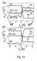
- Figure 9dshows time plots 44 and 45 of simultaneously-measured (i.e. simultaneous with the measurements shown in Figures 9a, 9b and 9c) transverse Hall and longitudinal Hall resistance R H , R L .
- the transverse Hall resistance, R Hmeasured using the second Hall probe 19 1 , 19 2 , depends only on the light polarization.
- the transverse Hall resistance, R His zero at linear polarization ⁇ 0 and changes sign for opposite circular polarized light ⁇ ⁇ .
- plots of Hall resistances 51 1 , 51 2 , 51 3 as shown measured by the three pairs of 2DEG Hall probes 18 1 , 18 2 , 19 1 , 19 2 , 20 1 , 20 2 at a reverse bias of - 10 V at 4 °Kare shown.
- the presence and spatial non-uniformity of the Hall resistances 51 1 , 51 2 , 51 3are due to spin-orbit coupling effects. Depending on the out-of-plane component of their spin, electrons are asymmetrically deflected towards the edges of the 2DEG channel creating a finite Hall voltage.
- the spatial dependence of the signalreflects the reciprocal effect of the coupled spin-charge dynamics in which spins rotate while passing along the 2DEG channel 15.
- the Hall signals 52, 53are linear in the degree of polarization and the magnitude of the Hall signals is large.
- the device 1( Figure 9 ) operates as a spin photovoltaic cell, i.e. it can operate even when no external electrical bias is applied. Both the longitudinal and Hall resistivities at zero bias remain comparable to the respective signals measured under reverse bias, yielding only weakly bias dependent Hall angles. The measured differences between the zero and finite bias Hall signals can be attributed to variations in the optical excitation conditions.
- plots of Hall signals 57 1 , 57 2 , 57 3 measured by the three 2DEG Hall probes 18 1 , 18 2 , 19 1 , 19 2 , 20 1 , 20 2 ( Figure 9 ) at zero bias at 230 °Kare shown.
- an upper bound for the spin-precession wavelengthcan be inferred, estimated from the measurements made by the three Hall probes 18 1 , 18 2 , 19 1 , 19 2 , 20 1 , 20 2 ( Figure 9 ) and which is of the order of a micrometre.
- a spin-coherence length of at least a few micrometrescan be observed as illustrated, for example, by the largest signal measured at the third Hall probe 20 1 , 20 2 ( Figure 9 ) at 230 °K.
- the 2DEG channel 15( Figure 9 ) can be used to achieve strong spin-charge coupling effects while maintaining large spin-coherence of diffusing carriers in 2D systems with Rashba and Dresselhaus spin-orbit coupling.
- Figure 14is a plot 58 of ⁇ H along the [1-10] direction for different ratios ⁇ /
- a third device 201is shown which can be used as polarimeter.
- the third device 201is similar to the second device 1. Again, no Hall contacts need be connected to the 2DHG channel 11. In this case, however, the device 201 includes two pairs of Hall contacts 18 1 , 18 2 , 19 1 , 19 2 connected to the 2DEG channel 15.
- the gate 61may comprise optically transparent material, such as indium-tin-oxide (ITO).
- ITOindium-tin-oxide
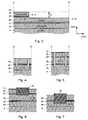
- the conditionis that x ⁇ 0.4 for region 28 and that x is larger in regions 26, 29, 30 compared to region 28.
Landscapes
- Physics & Mathematics (AREA)
- General Physics & Mathematics (AREA)
- Spectroscopy & Molecular Physics (AREA)
- Hall/Mr Elements (AREA)
- Measuring Magnetic Variables (AREA)
- Junction Field-Effect Transistors (AREA)
Description
- The present invention relates to a spin-polarised charge carrier device, particularly, but not exclusively, to a polarimeter.
WO 2005/109518 A describes a double-channel transistor comprising a first semiconductor layer (such as GaAs), a second semiconductor layer formed on the first layer having greater spin diffusion than the first layer, at least two ferromagnetic electrodes and at least one conductor electrode. The ferromagnetic electrodes can be formed from a 3d transition metal or a ferromagnetic semiconductor, such as cobalt-substituted zinc oxide doped with aluminium.WO 2008/005719 A describes a spin injector which includes an array of ferromagnetic elements disposed within a semiconductor. The ferromagnetic elements are arranged and spaced with respect to one another in a close arrangement such that electrons of holes are spin-polarized when passing through. A spin injector can be located above or at least partially within source and drain regions of a field effect transistor formed from a semiconductor such as silicon.EP 1 501 134 A- A polarimeter can be used to measure changes in polarization caused by optical activity in materials, such as anisotropic crystalline solids and solutions containing chiral molecules.
- A conventional polarimeter usually consists of a pair of linear polarizers and a photodetector, such as a photodiode. Light from a monochromatic source passes sequentially though a first polarizer having a fixed orientation, the sample and a second polarizer (or "analyzer"). The photodetector is used to detect the intensity of light reaching it from the analyzer.
- Rotating the analyzer relative to the first polarizer varies the intensity of light teaching the photodetector. Thus, in the absence of an optically-active sample, the angle needed to minimize light intensity is 90°. However, in the presence of an optically-active sample, additional rotation, θ, is required.
- The need for mechanically rotating the analyzer can be avoided by using an electrically-controllable wave plate (or "retarder") to introduce a controlled amount of optical rotation and, thus, compensate for optical activity of the sample. Notwithstanding this, it is generally desirable to simplify the polarimeter.
- A polarimeter is described "All-electric detection of the polarization state of terahertz laser radiation", S. D. Ganichev, W. Weber, J. Kiermaier, S. N. Danilov, P. Olbrich, D. Schuh, W. Wegscheider, D. Bougeard, G. Abstreiter, and W. Prettl, Journal of Applied Physics,) in which longitudinal photogalvanic currents are determined by degree of linear polarization.
- The present invention seeks to provide a spin-polarised charge carrier device which, for example, which can be used as an improved polarimeter.
- According to a first aspect of the present invention there is provided a device comprising a channel for charge carriers comprising non-ferromagnetic semiconducting material in which charge carriers exhibit spin-orbit coupling, a region of semiconducting material of opposite conductivity type to the channel and configured so as to form a junction with the channel for injecting spin-polarised charge carriers into an end of the channel and at least one lead connected to the channel for measuring a transverse voltage across the channel.
- Thus, light can be used to generate spin-polarized charge carriers whose spin polarization is proportional to the degree of circular polarisation of the light and the charge carriers are transversely deflected depending on their local polarization in the channel.
- The channel may comprise a potential well confining a two-dimensional charge-carrier gas, such as a two-dimensional electron gas. The potential well may be asymmetric. The semiconducting material may be a crystal having no inversion symmetry. The semiconducting material may comprise a III-V semiconductor, such as GaAs or AlGaAs.
- The conductivity type of the region may be p-type and the conductivity type of the non-ferromagnetic semiconducting material may be n-type.
- The device may further comprise a gate configured to apply an electric field to the channel. This can be used to tune the device by varying the Rashba spin-orbit coupling strength which can result from an asymmetric confining potential, e.g. by ensuring it is equal to the Dresselhaus spin-orbit coupling strength which can result from a lack of inversion symmetry of the material in the channel.
- The leads may be arranged along one side or opposite sides of the channel. The at least one lead may comprise one or two leads spaced from the junction by a distance equal to about N.(xp/2), where N is a positive integer and xp = h/(4.m.α), where h is Plank's constant, m is the effective mass of the charge carrier and α is Rashba coupling constant.
- The at least one lead may comprise first and second leads connected to the channel between first and second ends and arranged on opposite sides of the channel for measuring a voltage difference across the channel.
- The at least one lead may comprises third and fourth leads connected to the channel and arranged on opposite sides of the channel for measuring a voltage difference across the channel, said third and fourth leads spaced apart along the channel from the first and second leads.
- The semiconducting material of opposite conductivity type may be non-ferromagnetic.
- According to a second aspect of the present invention there is provided a method of operating a device comprising a channel for charge carriers comprising non-ferromagnetic semiconducting material in which charge carriers exhibit spin-orbit coupling, a region of semiconducting material of opposite conductivity type to the channel and configured so as to form a junction with the channel for injecting spin-polarised charge carriers into an end of the channel and at least one lead connected to the channel for measuring a transverse voltage across the channel, the method comprising illuminating the junction with light and measuring bias(es) at the lead(s).
- The method may further comprise applying a bias between the region and a second end of the channel.
- According to a third aspect of the present invention there is provided a method of fabricating a device, the method comprising providing a channel for charge carriers comprising non-ferromagnetic semiconducting material in which charge carriers exhibit spin-orbit coupling, providing a region of semiconducting material of opposite conductivity type to the channel and configured so as to form a junction with the channel for injecting spin-polarised charge carriers into an end of the channel and providing at least one lead connected to the channel for measuring a transverse voltage across the channel.
- The method may comprise providing a layer structure comprising first and second adjacent and/or overlying channels and etching a portion of one of the channels so as to leave the region and the channel.
- Embodiments of the present invention will now be described, by way of example, with reference to the accompanying drawings in which:
Figure 1 is a perspective schematic view of a device in accordance with the present invention;Figure 1a illustrates a layer structure used to form the device shown inFigure 1 ;Figure 2 is a plan view of the device shown inFigure 1 ;Figure 3 is a cross section view of the device shown inFigures 1 and 2 taken along the line A-A;Figure 4 is a cross section view of the device shown inFigures 1 and 2 taken along the line B-B';Figure 5 is a cross section view of the device shown inFigures 1 and 2 taken along the line C-C';Figure 6 is a cross section view of an ohmic contact to a first conductive layer in the device shown inFigures 1 and 2 ;Figure 7 is a cross section view of an ohmic contact to a first conductive in the device shown inFigures 1 and 2 ;Figure 8 is a process flow diagram of a method of fabricating the device shown inFigures 1 and 2 ;Figure 9 illustrates measurement of the device shown inFigures 1 and 2 ;Figures 10a to 10d illustrates plots of light intensity, photocurrent, longitudinal voltage and Hall resistances in time;Figure 11 is a plot of Hall resistance with time for three different sets of probes for the device shown inFigures 1 and 2 ;Figures 12a to 12d are plots of Hall signals at different parts of the device shown inFigures 1 and 2 as a function of degree of circular polarisation;Figure 13a is a plot of Hall resistance with time for three different sets of probes for the device shown inFigure 1 in the absence of applied bias taken at 4 °K;Figure 13b is a plot of Hall resistance with time for three different sets of probes for the device shown inFigure 1 in the absence of applied bias taken at 230 °K;Figure 14 is a plot of Hall angle for different values of Rashba and Dresselhaus constants;Figure 15 illustrates precession of charge carrier spin along a channel for three different ratios of Rashba and Dresselhaus constants;Figure 16 illustrates another embodiment of a device in accordance with the present invention;Figure 17 illustrates yet another embodiment of a device in accordance with the present invention;Figure 18 illustrates a gate for tuning a device; andFigure 19 illustrates effect of a surface gate on a potential well forming a two-dimensional electron gas.- Referring to
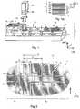
Figures 1, 1a and2 to 5 , an electro-optical, spin-polarisedcharge carrier device 1 is shown. Thedevice 1 comprises amesa 2 defined by trench isolation usingetched trenches 3. Themesa 2 is used to pattern an aluminium gallium arsenide/gallium arsenide (AlGaAs/GaAs)heterostructure 4 on an undoped GaAs substrate 5 (Figure 1a ). Themesa 2 is stepped having upper,un-etched level 61 and lower, etchedlevel 62. Thus, themesa 2 is divided into first andsecond parts step edge 7. Themesa 2 is stepped so as to form a two-dimensional hole gas (2DHG) 8 in the first part of themesa 21 and a two-dimensional electron gas (2DEG) 9 in the second part of themesa 22. The2DEG 9 is populated with electrons having a sheet concentration n2DEG = 2.5×1011 cm-2 and a mobility of µ = 3×103 cm2/Vs. However, a portion 9' of the 2DEG which lies beneath the2DHG 8 is depleted. - The
mesa 2 includes aHall bar structure 10 which crosses thestep edge 7. Thestructure 10 defines anelongate 2DHG channel 11 extending between a first end and asecond end 13 and having a pair oflateral Hall contacts 141, 142 (or "probes") for sensing a transverse voltage across thechannel 11. Thestructure 10 also defines anelongate 2DEG channel 15 extending betweenfirst end 16 and a second end and having three pair oflateral probes channel 15, each pair ofprobes channel 15. - The
channels 2DHG Hall contacts contacts Hall bar contacts Hall bar contacts Hall bar contacts 2DEG Hall contacts - A
p-n junction 21 is formed between thesecond end 13 of the2DHG channel 11 and thefirst end 16 of the2DEG channel 15 beneath thestep edge 7. - A
laser 22, tuned to a wavelength of about 850 nm, is used to illuminate aspot 23 having a diameter of about 1 µm in the vicinity of thestep edge 7 from the2DHG 8. Under illumination, photo-excited electrons and holes are driven in opposite directions in the respective 2DEG and2DHG channels elastic modulator 24. As will be explained later, thelaser 23 is also used to illuminate anotherspot 25 having a diameter of about 2 µm in the vicinity of the2DHG Hall contacts - Referring in particular to
Figures 1a , theheterostructure 4 includes alayer 26 of undoped Al03Ga0.7As having a thickness, t1, of about 300 nm. An n-type δ -dopedlayer 27 having a concentration of about 5×1012 cm-2 is embedded 3 nm from the upper surface of the Al03Ga0.7Aslayer 26. - The heterostructure further includes, a
layer 28 of undoped GaAs having a thickness, t2, of about 90 nm, aspacer layer 29 of undoped Al05Ga0.5As having a thickness, t3, of about 3 nm, alayer 30 of p-type Al05Ga0.5As having a thickness, t4, of about 47 nm and acapping layer 31 of p-type GaAs having a thickness, t5, of about 5 nm. - Where the
GaAs layer 28 is partially removed, e.g. by about 10 nm, and the overlying p-type layers heterostructure 4 are removed to form patterned layer 28', 29', 30', 31' a first conductive sheet of a first conductivity type, i.e. 2DHG 8, is formed in an upper part of the patterned undoped GaAs layer 28', while a second conductive sheet of a second conductivity type, i.e. a2DEG 9, is formed in a lower part of the same layer 28'. This technique is described inEP-A-1 501 134 . TheGasAs layer 28 need not be etched. - Referring to
Figure 6 , a AuZn alloy is used to form p-type ohmic contacts 33 to the 2DHGHall bar channel 11, which may define one end of thechannel 11, and other portions of the 2DHG 8 (Figure 1 ) providing the 2DHGHall bar contacts 141, 142 (Figure 1 ). - Referring to
Figure 7 , a AuGeNi alloy is used to form n-type contacts 34 to the 2DEGHall bar channel 15, which may define one end of thechannel 15, and other portions of the 2DEG 9 (Figure 1 ) providing the 2DEGHall bar contacts Figure 1 ). - Referring to
Figure 8 , a flow diagram of a method of fabricating thedevice 1 is shown. - Starting with a chip containing the layer structure 4 (
Figure 1a ), a pattern outlining the mesa 2 (Figure 2 ) is defined in a resist (not shown) (step S1). An electron-beam resist, namely polymethylmethacrylate (PMMA), is applied by spin coating to surface of the chip, an electron beam is used to expose selective areas of the resist and the resist is developed. - The pattern of the resist is transferred to the chip by anisotropic dry etching (step S2), namely a SiCl4/Ar reactive ion etch at 20 mTorr chamber pressure.
- The pattern of the 2DEG is defined in a resist (not shown) (step S3). Another layer of electron-beam resist is applied by spin coating to surface of the chip, an electron beam is used to expose selective areas of the resist and the resist is developed.
- The pattern of the resist is transferred to the chip by wet etching (step S4), namely using a slow, timed wet etch comprising H2SO4, H2O2 (30%) and H2O (1:8:1000).
- P-type ohmic contacts 33 (
Figure 6 ) to the 2DHG channel 11 (Figure 1 ) andHall probe electrodes 141, 142 (Figure 1 ) are fabricated (steps S5 to S8). The pattern of the p-type ohmic contacts is defined in optical resist (not shown) (step S5), material for forming a p-type ohmic contact, namely AuZn alloy (5% Zn by weight), is thermally evaporated (step S6) and unwanted regions of material are lifted off in acetone (step S7). The p-type ohmic contact is anneal (step S8) by annealing the sample for 5-minutes at 440 °C in a forming gas (5% H2 in N2). - N-type ohmic contacts 34 (
Figure 7 ) to the 2DEG channel 15 (Figure 1 ) and correspondingHall probe electrodes Figure 1 ) are fabricated (steps S9 to S12). The pattern of the n-type ohmic contacts are defined in optical resist (not shown) (step S9), material for forming an n-type ohmic contact, namely a AuGeNi alloy (AuGe 88:12, 5% Ni), is thermally evaporated (step S10) and unwanted regions of material are lifted off in acetone (step S11). The n-type ohmic contact is annealed (step S12) by annealing the sample for 5-minutes at 400 °C in a forming gas (5% H2 in N2). - Finally, large-area bond pads (not shown) for wire bonding are defined (steps S13 to S15). The pattern of the bond pads are defined in optical resist (not shown) (step S13), material for forming bond pads, namely a sticking layer of Cr followed by a layer of Au, is thermally evaporated (step S14) and unwanted regions of material are lifted off in acetone (step S15).
- Hall voltage signals and photocurrent are detected simultaneously using a lock-in technique, as will now be described:
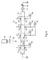
- Referring to
Figure 9 , a continuous wave Ti:sapphire laser 22 is used to generate abeam 35 of monochromatic light of adjustable wavelength in the near infrared sub-GaAs band-gap spectrum between 820 nm to 860 nm. After passing thebeam 35 through an attenuator (not shown), thebeam 35 is successively chopped at a low frequency of about 150 Hz. A successive beam splitter (not shown) combined with a photo-diode detector (not shown) and a successive lock-in amplifier (not shown) is employed to monitor intensity fluctuations of thebeam 35. - Using a linear polarizer and a λ/2 wave-plate, a second part of the
beam 35 is linearly polarized at 45° with respect to the optical axis of a photo-elastic modulator 24 with adjustable retardation and a modulator frequency of 50 kHz. Retardation of ± 90° generates circular left/right polarized light, retardation of 0° and 180° generates linearly polarized light at ±45°. - The
beam 35 is focused to a spot size of about 1µm on the optically active area of the lateral p-n junction Hall bar device by using a pin-hole (not shown) and a high-resolution microscope objective (not shown) mounted to a high precession piezoelectric x-y-z stage (not shown). An additional beam-splitter (not shown) combined with an objective (not shown) and a CCD camera (not shown) allows thebeam 35 to be aligned to Hall bar structure. - The
device 1 is mounted in an Oxford Instruments Microstat High Resolution continuous flow cryostat (not shown) with adjustable measurement temperature ranging from less than 4 °K up to room temperature. - A
voltage source 36 is used to reverse bias thep-n junction 21. Photo-excited current through the reverse biasedp-n junction 21 is measured using anarrangement 37 including a SR570 current preamplifier (not shown) connected to a lock in amplifier (not shown) with the reference frequency of the chopped light beam. - The intensity of the
beam 35 is attenuated to generate a photocurrent along the Hall bar of approximately 500 nA. The Hall probes 141, 142, 181, 182, 191, 192, 201, 202 are connected to SR560high impedance pre-amplifiers 38, 39 and are successively connected to lock-in amplifiers (not shown) with the reference frequency of the photo-elastic modulator 24. - An additional high-
impedance preamplifier 40 combined with a lock-in amplifier (not shown) is used to monitor a longitudinal voltage drop between two adjacentHall probe contacts - Referring to Figures 9a, 9b and 9c, time plots of simultaneously-measured
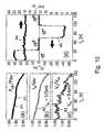
light intensity 41,photocurrent 42 andlongitudinal voltage 43 are shown. - Figures 9b and 9c show that as light intensity drifts, then the photocurrent and longitudinal voltage also drift.
- Figure 9d shows time plots 44 and 45 of simultaneously-measured (i.e. simultaneous with the measurements shown in Figures 9a, 9b and 9c) transverse Hall and longitudinal Hall resistance RH, RL.
- Figure 9d shows both Hall resistance, RH, and the longitudinal Hall resistance, RL, are independent of the light intensity variation.
- The transverse Hall resistance, RH, measured using the
second Hall probe - The larger variation of transverse Hall resistance, RH, at σ± can be attributed to a small drift of the beam spot and, therefore, the injection point of the spin-polarized current during the measurement time.
- Referring to
Figure 11 , plots ofHall resistances - The
Hall resistances Figure 9 ). Due to the optical selection rules, the spin-polarization of the injected carriers is determined by the polarization of the incident light. In other words, the sign of theHall resistances 511 512 513 reverses upon reversing the out-of-plane spin-polarization of the optically-generated conduction electrons. For a fixed helicity of light, theHall resistances planar 2DEG channel 15 change not only magnitude, but also sign. - The presence and spatial non-uniformity of the
Hall resistances 2DEG channel 15. - Referring to
Figures 12a and 12b ,dependences successive Hall contacts - As shown in
Figure 12a and 12b , the Hall signals 52, 53 are linear in the degree of polarization and the magnitude of the Hall signals is large. - Referring to
Figures 12c and 12d , dependences 53, 54 of Hall measurements in the2DHG channel 11 are shown. - In
Figure 12c , the measurement is taken with the beam 35 (Figure 9 ) located in the first spot 23 (Figure 9 ). InFigure 10d , the measurement is taken with the beam 35 (Figure 9 ) located in the second spot 25 (Figure 9 ). - As shown in
Figure 12c , no strong signal is found with the laser 35 (Figure 9 ) focused on the p-n junction 21 (Figure 9 ), i.e. in the first spot 23 (Figure 9 ). This is consistent with a substantially smaller spin coherence length in the strongly spin-orbit coupled 2DHG. - However, as shown in
Figure 12d , a strong transverse-voltage signal is observed when uniformly polarizing a larger area of the 2DHG channel 11 (Figure 9 ) around theHall probe 141, 142 (Figure 9 ). - Referring to
Figure 13a , plots of Hall signals 561, 562, 563 measured by the three 2DEG Hall probes 181, 182, 191, 192, 201, 202 (Figure 9 ) at zero bias at 4 °K are shown. - As shown in
Figure 13a , the device 1 (Figure 9 ) operates as a spin photovoltaic cell, i.e. it can operate even when no external electrical bias is applied. Both the longitudinal and Hall resistivities at zero bias remain comparable to the respective signals measured under reverse bias, yielding only weakly bias dependent Hall angles. The measured differences between the zero and finite bias Hall signals can be attributed to variations in the optical excitation conditions. - Referring to
Figure 13b , plots of Hall signals 571, 572, 573 measured by the three 2DEG Hall probes 181, 182, 191, 192, 201, 202 (Figure 9 ) at zero bias at 230 °K are shown. - The p-n junction leakage current is still negligible.
Figure 13b demonstrates that the photovoltaic and spin-orbit coupling effects are readily detectable at high temperatures. - Although the spin-generation conditions vary with changing temperature due to thermal drifts, the following observations can be made.
- Firstly, at all measured temperatures, an upper bound for the spin-precession wavelength can be inferred, estimated from the measurements made by the three Hall probes 181, 182, 191, 192, 201, 202 (
Figure 9 ) and which is of the order of a micrometre. - Secondly, a spin-coherence length of at least a few micrometres can be observed as illustrated, for example, by the largest signal measured at the
third Hall probe 201, 202 (Figure 9 ) at 230 °K. This implies that multiple-probe planar structures can be fabricated, for example, by electron-beam lithography and used for detailed studies of spin-precession and decoherence effects in 2D semiconductor channels. - Thirdly, external electric gates can be used to control spin-dynamics and so provide a means for realizing and exploring the Datta-Das transistor functionality beyond the originally-proposed concept based on longitudinal transport detection scheme.
- Fourthly, the 2DEG channel 15 (
Figure 9 ) can be used to achieve strong spin-charge coupling effects while maintaining large spin-coherence of diffusing carriers in 2D systems with Rashba and Dresselhaus spin-orbit coupling. - The behaviour can be described based on the observation that the micrometer length scale governing the spatial dependence of the non-equilibrium spin-polarization is much larger that the ∼20 nm mean-free-path in the 2DEG channel 11 (
Figure 9 ) which governs the transport coefficients. - This allows the steady-state spin-polarization profile along the channel to be calculated and then consider the spin-injection Hall effect as a response to the local out-of-plane component of the polarization.
- Calculations start from the electronic structure of GaAs whose conduction band near the Γ-point is formed dominantly by Ga s-orbitals. This implies weak spin-orbit coupling originating from the mixing of the valence-band p-orbitals and from the broken inversion symmetry in the zincblende lattice.
- In the presence of an electric potential, the corresponding 3D spin-orbit coupling Hamiltonian is

where σ are the spin Pauli matrices,k is the momentum of the electron,≈ 10 eVÅ3, and λ*= 5.3 Å2 for GaAs. Equation (1) above, together with the 2DEG confinement yield an effective 2D Rashba and Dresselhaus spin-orbit couple Hamiltonian, namely:

where
Figure 1a ). - The parameter λ* is the spin-orbit strength which can be calculated by:

where Eg is the band gap and p is the momentum operator and Δso is the spin-orbit split-off hole band position. - In the weak spin-orbit coupling regime of our structure with αkF and βkF (∼0.5 meV) much smaller than the disorder scattering rate ℏ/τ (∼5 meV), the system obeys a set of spin-charge diffusion equations. In the steady-state, the spatial dependence of the out-of-plane component of the spin polarization along the [1-10] channel direction is given by a damped oscillatory function

with the complex wavevector
where

and
- From the known local spin-polarization, the Hall signal can be calculated by taking into account that the dominant contribution in the weak spin-orbit coupling regime is the extrinsic skew scattering. This contribution is obtained by considering asymmetric scattering from a spin-orbit coupled impurity potential originating from the first term in equation (1) above.
- Within the second-order Born approximation for delta-function scatterers, a spatially dependent spin-injection Hall effect angle and be obtained, namely:

where n is the density of optically injected carriers into the 2DEG channel 15 (Figure 8 ). Figure 14 is aplot 58 of αH along the [1-10] direction for different ratios α/|β| of Rashba and Dresselhaus parameters.- It has been assumed that the donor impurity densityni is of the order of the equilibrium density n2DEG of the 2DEG channel 15 (
Figure 8 ) in dark, which provides an upper bound for the strength of the impurity scattering in the modulation-doped heterostructure and, therefore, a lower bound for the Hall angle. It has also been assumed that the mobility of the 2DEG channel 15 (Figure 8 ) is the same as that determined from an ordinary Hall measurement without illumination. The density of photoexcited carriers ofn ≈ 2 × 1011 cm-2 was obtained from the measured longitudinal resistance between successive Hall probes under illumination assuming constant mobility. - The
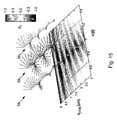
plot 58 shown inFigure 14 is consistent with the measured behaviour of the device and the value of the precession length obtained by the calculation and the value inferred from experiment are consistent. Figure 15 shows how spin precesses along the 2DEG channel 15 (Figure 8 ) for three different values of α/|β|, namely 0.7, 1.0, 1.3.Figure 15 shows that if spin-polarized electrons with polarization along the [1-10] crystalline orientation are injected at a point X0 and propagate through a 2D system at spin-Helix conditions, the perpendicular-to-the-plane-oriented polarization of the injected electrons recovers at multiples of xP=h/(4.m.α) along the [1-10] orientation, where h is Plank's constant, m is the effective mass of the electron and α is the Rashba spin-orbit interaction term. The length, xP, is independent of the number of times the electron scatters from the injection point, x0, to xPN= N.xP, where N is an integer. Between xPN and xP(N+1), electron polarization completes one full precession as shown inFigure 14 .- In case of the absence of a Dresselhaus term or when there is a large difference between |α| and |β|, the net spin polarization of the electron current will dephase and spin-polarization lost, typically within a sub-micrometer length scale.
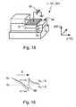
- Referring to
Figure 16 , a second,simpler device 101 is shown. - The
second device 101 is similar to thedevice 1 described earlier. However, no Hall contacts need be connected to the2DHG channel 11 and thedevice 101 may include only one pair ofHall contacts 2DEG channel 15 spaced from thep-n junction 21 by a distance, 1. - A quarter-wave plate 60 (or "λ/4 plate") can be used to convert linearly-polarized
light 61, σ0, into circularlypolarized light 62, σ+. The Hall voltage is proportional to the degree of linear polarization with thepolarization plane 45° to the optical axis of the quarter-wave plate 60. - The
Hall contacts p-n junction 21 by adistance 1 = N.xp/2 = N.(h/8.m.α) where N is an integer. The length, lcon, of thecontact - The
device 101 exploits the spin helix. In the case that α≅+(-)β, then the spin polarization precesses within the [001]/[110] (or [001]/1-10]) plane and the local spin-injection Hall effect signal (which is proportional to the z-component of the polarization vector) along the [001] / [110] channel direction can be detected. The magnitude of the signal is maximal if the contacts are at an integer number of half of the precession length from the injection area. - The
Hall contacts p-n junction 21 by adistance 1 < xp/2. Thus, polarization is detected in an area which is close to the injection area. The length, lcon, of thecontact - The
Hall contacts p-n junction 2, i.e. l = 0. Thus, polarization is detected across the injection area. The length, lcon, of thecontacts - Referring to
Figure 17 , athird device 201 is shown which can be used as polarimeter. - The
third device 201 is similar to thesecond device 1. Again, no Hall contacts need be connected to the2DHG channel 11. In this case, however, thedevice 201 includes two pairs ofHall contacts 2DEG channel 15. The first set ofHall contacts p-n junction 21 by a distance l1= N.xp/2 = N.(h/8.m.α) and the second set ofHall contacts - Thus, the first set of
contacts contacts - Referring to
Figure 18 , thedevices gate electrode 63 on thesurface 64 of thelower step mesa 22 for applying a vertical electric field to the2DEG channel 15 between thejunction 21 and the first set ofHall contacts 181 usingvoltage source 65. - The
gate 61 may comprise optically transparent material, such as indium-tin-oxide (ITO). - Referring also to
Figure 19 , thegate 61 can be used to apply an a field E whereby apotential well 66 forming the2DEG 9 can be made more asymmetric and, thus, change the value of Rashba coupling constant, α. Thus, the device can used to trim the device to ensure that α/|β| = 1.0 and/or that the Hall contacts produce the maximum signal. - It will be appreciated that many modifications may be made to the embodiments hereinbefore described.
- For example, the 2DEG and 2DHG layers can be inverted so that the 2DEG layer lies above the 2DHG layer. However, in this case, the 2DEG confining field is negative in the direction of [001] (i.e. as opposed to being positive along [001] as described earlier) and so the channel should be arranged, for example, so that electrons are injected into a channel in the [110] direction.
- Furthermore, different material systems may be used. For example, with reference to
Figure 3 , A1xGa1-xAs with x>0 may be used forregion 28, instead of x=0 as described above. The condition is that x<0.4 forregion 28 and that x is larger inregions region 28. - In addition, with the same condition for x with respect to
regions region 28 on the other hand, the following III-V material systems may be used, instead of A1xGa1-xAs: - In1-xAlxAs (x=0...0.7)
- InxGaxAs (x=0...1)
- GaAsxP1-x (x=0...0.5)
- Ga1-xAlxSb (x=0...0.3)
- InAs1-xPx (x=0..1)
- ALxGa1-xN (x=0...1)
- In1-xGaxN (x=0...1)
- Also combinations of these systems are possible, as long as the bandgap of
region 28 is smaller than the bandgap ofregions - The following II-VI system can also be used, with the same restriction on x, comparing
regions region 28 on the other side: - CdxHg1-xSe
- TeHg1-xCdx
- Hg1-xZnxSe
- ZnxCd1-xSe
- ZnSxSe1-x
- ZnsxTe1-x
- The dimensions of the devices can be changed. For example, the width of the channel, w, may be made smaller, e.g. between about 100 nm and 1 µm, or larger, e.g. between about 1 µm and 10 µm. The length of the channels can also vary. The size and configuration of the Hall contacts can be varied.
- The channel may be formed in other ways. For example, a double barrier heterostructure, e.g. AlGaAg/GaAs/AlGaAs can be used to form a planar, i.e. 2D, conductive sheet.
- There can be only one lead or only leads along one side of the channel, i.e. the leads need not be arranged on opposite sides of the channel. Thus, a Hall measurement can be taken using one lead and compared to a reference, e.g. ground.
- An implanted well can be used to provide one or both halves of the
p-n junction 21. Thus, the device may comprise a AlGaAs/GaAs heterostructure providing a 2DEG channel and p-type impurities may be implanted to form the junction.


Claims (16)
- A device comprising:a channel (15) for charge carriers comprising non-ferromagnetic semiconducting material in which charge carriers exhibit spin-orbit coupling;a region (10) of semiconducting material of opposite conductivity type to the channel and configured so as to form a junction (21) with the channel for injecting spin-polarised charge carriers into an end of the channel; andat least one lead (181, 182,191, 192) connected to the channel for measuring a transverse voltage across the channeL
- A device according to claim 1, wherein the channel (15) comprises a potential well (66) confining a two-dimensional charge-carrier gas (9).
- A device according to claim 2, wherein the potential well (66) is asymmetric.
- A device according to any preceding claim, wherein the semiconducting material is a crystal having no inversion symmetry.
- A device according to any preceding claim, wherein the non-ferromagnetic conductive material comprises a III-V semiconducting material.
- A device according to any preceding claim, wherein the conductivity type of the region is p-type and the conductivity type of the channel is n-type.
- A device according to any preceding claim, further comprising:a gate (61) configured to apply an electric field to the channel.
- A device according to any preceding claim, wherein the leads (181, 182,191, 192) are arranged along one side or opposite sides of the channel (15).
- A device according to any preceding claim, wherein the at least one lead (181, 182,191, 192) comprises:one or two leads (181, 182) spaced from the junction by a distance (1) equal to about N.(xp/2), where N is a positive integer and xp = h/(4.m.α), where h is Plank's constant, m is the effective mass of the charge carrier and α is Rashba coupling constant.
- A device according to any preceding claim, wherein the at least one lead (181, 182,191, 192) comprises:first and second leads (181, 182) connected to the channel and arranged on opposite sides of the channel for measuring a voltage difference across the channel.
- A device according to claim 10, wherein the at least one lead (181, 182,191, 192) comprises.
third and fourth leads (191, 192) connected to the channel and arranged on opposite sides of the channel for measuring a voltage difference across the channel, said third and forth leads spaced apart along the channel from the first and second leads. - A device according to any preceding claim, wherein the semiconducting material of opposite conductivity type to the channel is noo-ferromagnetic.
- A method of operating device comprising a channel (15) for charge carriers comprising non-ferromagnetic semiconducting material in which charge carriers exhibit spin-orbit coupling, a region (10) of semiconducting material of opposite conductivity type to the channel and configured so as to form a junction (21) with the channel for injecting spin-polarised charge carriers into an end of the channel and at least one lead (181, 182, 191, 192) connected to the channel for measuring a transverse voltage across the channel, the method comprising:illuminating the junction (21) with light; andmeasuring bias(es) at the lead(s).
- A method according to claim 13 further comprising:applying a reverse bias between the region (10) and another end of the channel.
- A method of fabricating a device, the method comprising:providing a channel (15) for charge carriers comprising non-ferromagnetic semiconducting material in which charge carriers exhibit spin-orbit coupling,providing a region (10) of semiconducting material of opposite conductivity type to the channel and configured so as to form a junction (21) with the channel for injecting spin-polarised charge carriers into an end of the channel andproviding at least one lead (181, 182, 191, 192) connected to the channel for measuring a transverse voltage across the channel.
- A method according to claim 15, the method comprising:providing a layer structure comprising first and second overlying channels; andetching a portion of one of the channels so as to leave the region and the channel.
Priority Applications (6)
| Application Number | Priority Date | Filing Date | Title |
|---|---|---|---|
| EP08169560AEP2190022B1 (en) | 2008-11-20 | 2008-11-20 | Spin-polarised charge carrier device |
| US12/545,502US9000433B2 (en) | 2008-11-20 | 2009-08-21 | Spin-polarised charge-carrier device |
| CN2009101684017ACN101738374B (en) | 2008-11-20 | 2009-08-24 | Spin Polarized Carrier Devices |
| KR1020090077918AKR20100056960A (en) | 2008-11-20 | 2009-08-24 | Spin-polarised charge carrier device |
| TW098128390ATW201022650A (en) | 2008-11-20 | 2009-08-24 | Spin-polarised charge carrier device |
| JP2009251998AJP2010122211A (en) | 2008-11-20 | 2009-11-02 | Spin photoelectric device |
Applications Claiming Priority (1)
| Application Number | Priority Date | Filing Date | Title |
|---|---|---|---|
| EP08169560AEP2190022B1 (en) | 2008-11-20 | 2008-11-20 | Spin-polarised charge carrier device |
Publications (2)
| Publication Number | Publication Date |
|---|---|
| EP2190022A1 EP2190022A1 (en) | 2010-05-26 |
| EP2190022B1true EP2190022B1 (en) | 2013-01-02 |
Family
ID=40474914
Family Applications (1)
| Application Number | Title | Priority Date | Filing Date |
|---|---|---|---|
| EP08169560ANot-in-forceEP2190022B1 (en) | 2008-11-20 | 2008-11-20 | Spin-polarised charge carrier device |
Country Status (6)
| Country | Link |
|---|---|
| US (1) | US9000433B2 (en) |
| EP (1) | EP2190022B1 (en) |
| JP (1) | JP2010122211A (en) |
| KR (1) | KR20100056960A (en) |
| CN (1) | CN101738374B (en) |
| TW (1) | TW201022650A (en) |
Cited By (1)
| Publication number | Priority date | Publication date | Assignee | Title |
|---|---|---|---|---|
| EP3435433B1 (en)* | 2017-07-27 | 2025-01-08 | Korea Institute of Science and Technology | Reconfigureable logic device using electrochemical potential |
Families Citing this family (21)
| Publication number | Priority date | Publication date | Assignee | Title |
|---|---|---|---|---|
| RU2452924C1 (en)* | 2010-12-27 | 2012-06-10 | Геннадий Михайлович Михеев | Method of determining circular polarisation sign of laser radiation |
| JP5880937B2 (en)* | 2011-12-22 | 2016-03-09 | 国立大学法人埼玉大学 | Spin polarization measurement method and measurement meter, and logic operation gate and signal encryption / decryption method using the same |
| EP2610913A1 (en) | 2011-12-30 | 2013-07-03 | Hitachi Ltd. | Spin-based device |
| GB2502312A (en)* | 2012-05-24 | 2013-11-27 | Ibm | Logic gates using persistent spin helices |
| CN103512653B (en)* | 2012-06-29 | 2016-12-21 | 新昌县冠阳技术开发有限公司 | A kind of device of the light logic gates measuring reflection light |
| EP2887403A4 (en)* | 2012-08-14 | 2015-09-02 | Japan Science & Tech Agency | SPIN POLARIZATION TRANSISTOR ELEMENT |
| US9548382B2 (en) | 2012-10-12 | 2017-01-17 | Northeastern University | Spintronic device |
| KR101699780B1 (en)* | 2012-11-08 | 2017-01-25 | 고쿠리츠켄큐카이하츠호진 카가쿠기쥬츠신코키코 | Spin valve element |
| US9429633B2 (en) | 2013-02-11 | 2016-08-30 | HGST Netherlands B.V. | Magnetic sensor utilizing rashba effect in a two-dimensional conductor |
| US20150041820A1 (en)* | 2013-08-12 | 2015-02-12 | Philippe Renaud | Complementary gallium nitride integrated circuits and methods of their fabrication |
| EP2982950A1 (en)* | 2014-08-08 | 2016-02-10 | Centre National De La Recherche Scientifique -Cnrs- | Process of detection of light and associated device |
| CN104779304B (en)* | 2015-04-02 | 2017-03-01 | 福州大学 | A kind of regulation and control Spectrum of Semiconductor Quantum Wells Rashba and the method for Dresselhaus Quantum geometrical phase ratio |
| CN105259490B (en)* | 2015-11-04 | 2018-08-17 | 福州大学 | A method of distinguishing the photic intrinsic mechanism of extraordinary Hall effect and extrinsic mechanism |
| US9564523B1 (en)* | 2015-12-11 | 2017-02-07 | International Business Machines Corporation | Non-linear spin-orbit interaction devices and methods for current-to-spin conversion and amplification of spin-polarizations |
| EP3276372B1 (en) | 2016-07-29 | 2021-04-14 | Datalogic IP Tech S.r.l. | Method and apparatus for sensing transparent and/or shining objects |
| CN106684240B (en)* | 2016-11-29 | 2019-03-01 | 北京航空航天大学 | A kind of super low-power consumption spin logical device based on nonferromagnetic material |
| CN108886061B (en)* | 2017-02-27 | 2021-11-16 | Tdk株式会社 | Spin current magnetization rotating element, magnetoresistance effect element, and magnetic memory |
| EP3776678A1 (en) | 2018-04-09 | 2021-02-17 | Yeda Research and Development Co. Ltd. | Device for electric field induced local magnetization |
| CN111276536B (en)* | 2020-02-07 | 2021-11-30 | 中国科学院半导体研究所 | Spin field effect transistor |
| CN113237834B (en)* | 2021-07-08 | 2021-09-14 | 成都信息工程大学 | Chiral molecule chiral resolution device and method based on optical spin Hall effect |
| WO2023018893A1 (en)* | 2021-08-11 | 2023-02-16 | The University Of Chicago | Optically controllable mesoscopic spin order in semiconductors |
Family Cites Families (74)
| Publication number | Priority date | Publication date | Assignee | Title |
|---|---|---|---|---|
| GB9125727D0 (en)* | 1991-12-03 | 1992-01-29 | Hitachi Europ Ltd | Non-linear optical device |
| US5648913A (en)* | 1993-03-29 | 1997-07-15 | Xilinx, Inc. | Frequency driven layout system and method for field programmable gate arrays |
| JP3351651B2 (en)* | 1995-04-07 | 2002-12-03 | 富士通株式会社 | Interactive circuit design equipment |
| US5652445A (en)* | 1995-04-21 | 1997-07-29 | Johnson; Mark B. | Hybrid hall effect device and method of operation |
| US5732246A (en)* | 1995-06-07 | 1998-03-24 | International Business Machines Corporation | Programmable array interconnect latch |
| US5701441A (en)* | 1995-08-18 | 1997-12-23 | Xilinx, Inc. | Computer-implemented method of optimizing a design in a time multiplexed programmable logic device |
| US5629637A (en)* | 1995-08-18 | 1997-05-13 | Xilinx, Inc. | Method of time multiplexing a programmable logic device |
| US5764954A (en)* | 1995-08-23 | 1998-06-09 | International Business Machines Corporation | Method and system for optimizing a critical path in a field programmable gate array configuration |
| US5822217A (en)* | 1995-12-13 | 1998-10-13 | Synopsys, Inc. | Method and apparatus for improving circuit retiming |
| JPH09231788A (en)* | 1995-12-19 | 1997-09-05 | Fujitsu Ltd | Shift register, programmable logic circuit, and programmable logic circuit system |
| US5914906A (en)* | 1995-12-20 | 1999-06-22 | International Business Machines Corporation | Field programmable memory array |
| JP3856892B2 (en)* | 1997-03-03 | 2006-12-13 | 日本電信電話株式会社 | Self-synchronous pipeline data path circuit and asynchronous signal control circuit |
| US6178275B1 (en)* | 1997-05-01 | 2001-01-23 | The Trustees Of The Stevens Institute Of Technology | Method and apparatus for modulation of guided plasmons |
| US6396302B2 (en)* | 1999-02-25 | 2002-05-28 | Xilinx, Inc. | Configurable logic element with expander structures |
| US6381171B1 (en)* | 1999-05-19 | 2002-04-30 | Kabushiki Kaisha Toshiba | Magnetic element, magnetic read head, magnetic storage device, magnetic memory device |
| US6874135B2 (en)* | 1999-09-24 | 2005-03-29 | Nec Corporation | Method for design validation using retiming |
| US6297987B1 (en)* | 1999-09-30 | 2001-10-02 | The United States Of America As Represented By The Secretary Of The Navy | Magnetoresistive spin-injection diode |
| JP2003526210A (en)* | 2000-02-29 | 2003-09-02 | コーニンクレッカ フィリップス エレクトロニクス エヌ ヴィ | Semiconductor device and manufacturing method thereof |
| JP3284239B2 (en)* | 2000-03-07 | 2002-05-20 | 東北大学長 | Spin-polarized conduction electron generation method and semiconductor device |
| US20020186584A1 (en)* | 2000-03-14 | 2002-12-12 | Mcdowell Joseph | High-efficiency miniature magnetic integrated circuit structures |
| US6469540B2 (en)* | 2000-06-15 | 2002-10-22 | Nec Corporation | Reconfigurable device having programmable interconnect network suitable for implementing data paths |
| US6675309B1 (en)* | 2000-07-13 | 2004-01-06 | Xilinx, Inc. | Method for controlling timing in reduced programmable logic devices |
| GB0022328D0 (en)* | 2000-09-12 | 2000-10-25 | Univ Cambridge Tech | An optically addressed spin-polarised diode |
| US6667862B2 (en)* | 2001-02-20 | 2003-12-23 | Carnegie Mellon University | Magnetoresistive read head having permanent magnet on top of magnetoresistive element |
| EP1310962A1 (en)* | 2001-11-08 | 2003-05-14 | Hitachi Ltd. | Magnetic memory cell |
| US6578183B2 (en)* | 2001-10-22 | 2003-06-10 | Silicon Perspective Corporation | Method for generating a partitioned IC layout |
| US6545329B1 (en)* | 2001-10-23 | 2003-04-08 | Mcnc | High sensitivity polarized-light discriminator device |
| US7073158B2 (en)* | 2002-05-17 | 2006-07-04 | Pixel Velocity, Inc. | Automated system for designing and developing field programmable gate arrays |
| US6879012B2 (en)* | 2002-06-21 | 2005-04-12 | The Regents Of The University Of California | Giant planar hall effect in epitaxial ferromagnetic semiconductor devices |
| US6829756B1 (en)* | 2002-09-23 | 2004-12-07 | Xilinx, Inc. | Programmable logic device with time-multiplexed interconnect |
| US7107568B2 (en)* | 2002-10-07 | 2006-09-12 | Hewlett-Packard Development Company, Lp. | System and method for reducing wire delay or congestion during synthesis of hardware solvers |
| US20060138397A1 (en)* | 2002-12-16 | 2006-06-29 | Mattis Daniel C | Manipulation of conductive and magnetic phases in an electron trapping semiconducting |
| US6943605B2 (en)* | 2002-12-31 | 2005-09-13 | Intel Corporation | Scan cell designs for a double-edge-triggered flip-flop |
| FR2851055B1 (en)* | 2003-02-12 | 2005-04-15 | Optogone Sa | DEVICE FOR SPATIAL MODULATION OF A LIGHT BEAM, AND CORRESPONDING APPLICATIONS |
| US7528428B2 (en)* | 2003-03-07 | 2009-05-05 | Japan Science And Technology Agency | Field-effect transistor with spin-dependent transmission characteristics and non-volatile memory using the same |
| KR100511077B1 (en)* | 2003-03-14 | 2005-08-30 | 한국과학기술연구원 | Hybrid ferromagnet/semiconductor spin device and fabrication method thereof |
| US7203919B2 (en)* | 2003-03-19 | 2007-04-10 | Peter Suaris | Retiming circuits using a cut-based approach |
| JP4500257B2 (en)* | 2003-03-31 | 2010-07-14 | 独立行政法人科学技術振興機構 | Tunnel transistor having spin-dependent transfer characteristics and nonvolatile memory using the same |
| US7064577B1 (en)* | 2003-05-02 | 2006-06-20 | Altera Corporation | Method and apparatus for supporting variable speed configuration hardware |
| US7162704B2 (en)* | 2003-05-09 | 2007-01-09 | Synplicity, Inc. | Method and apparatus for circuit design and retiming |
| US7120883B1 (en)* | 2003-05-27 | 2006-10-10 | Altera Corporation | Register retiming technique |
| RU2340032C2 (en)* | 2003-07-22 | 2008-11-27 | Йеда Рисеч Энд Девелопмент Компани Лтд. | Device for production of electronic emission |
| EP1501134A1 (en) | 2003-07-25 | 2005-01-26 | Hitachi, Ltd. | LED with a lateral pn-junction and a structure to control the emission of photons |
| US7274080B1 (en)* | 2003-08-22 | 2007-09-25 | International Business Machines Corporation | MgO-based tunnel spin injectors |
| US7088136B1 (en)* | 2003-11-06 | 2006-08-08 | Altera Corporation | Programmable logic device latch circuits |
| US6987484B2 (en)* | 2003-11-07 | 2006-01-17 | Max-Planck-Gesellschaft Zur Forderung Der Wissenschaften E.V. | Detector for electromagnetic radiation and a method of detecting electromagnetic radiation |
| US6963091B1 (en)* | 2003-12-22 | 2005-11-08 | National Semiconductor Corporation | Spin-injection devices on silicon material for conventional BiCMOS technology |
| WO2005065037A2 (en)* | 2004-01-08 | 2005-07-21 | Yeda Research And Development Company Ltd. | A device for the manipulation of current |
| US7109752B1 (en)* | 2004-02-14 | 2006-09-19 | Herman Schmit | Configurable circuits, IC's, and systems |
| FR2870045B1 (en)* | 2004-05-07 | 2006-07-21 | Thales Sa | DOUBLE CHANNEL FERROMAGNETIC / SEMICONDUCTOR HETEROJUNCTION DEVICE |
| US7411235B2 (en)* | 2004-06-16 | 2008-08-12 | Kabushiki Kaisha Toshiba | Spin transistor, programmable logic circuit, and magnetic memory |
| US7342415B2 (en)* | 2004-11-08 | 2008-03-11 | Tabula, Inc. | Configurable IC with interconnect circuits that also perform storage operations |
| EP1715356A1 (en)* | 2005-04-21 | 2006-10-25 | Interuniversitair Microelektronica Centrum ( Imec) | Spin detection device and methods for use thereof |
| US7496879B2 (en)* | 2004-12-01 | 2009-02-24 | Tabula, Inc. | Concurrent optimization of physical design and operational cycle assignment |
| US7800097B2 (en)* | 2004-12-13 | 2010-09-21 | Panasonic Corporation | Semiconductor device including independent active layers and method for fabricating the same |
| EP1705665B1 (en)* | 2005-03-24 | 2008-04-02 | Hitachi Ltd. | Conduction control device |
| EP1907957A4 (en)* | 2005-06-29 | 2013-03-20 | Otrsotech Ltd Liability Company | Methods and systems for placement |
| US7484194B2 (en)* | 2005-07-18 | 2009-01-27 | Synopsys, Inc. | Automation method and system for assessing timing based on Gaussian slack |
| US7372297B1 (en)* | 2005-11-07 | 2008-05-13 | Tabula Inc. | Hybrid interconnect/logic circuits enabling efficient replication of a function in several sub-cycles to save logic and routing resources |
| US7489162B1 (en)* | 2005-12-01 | 2009-02-10 | Tabula, Inc. | Users registers in a reconfigurable IC |
| EP1830410A1 (en)* | 2006-02-24 | 2007-09-05 | Hitachi, Ltd. | Single-charge tunnelling device |
| US20080012004A1 (en)* | 2006-03-17 | 2008-01-17 | Mears Technologies, Inc. | Spintronic devices with constrained spintronic dopant |
| US7625767B2 (en)* | 2006-03-17 | 2009-12-01 | Mears Technologies, Inc. | Methods of making spintronic devices with constrained spintronic dopant |
| DE602006013106D1 (en)* | 2006-06-13 | 2010-05-06 | Hitachi Ltd | Magnetoresistance device |
| KR100709395B1 (en)* | 2006-06-23 | 2007-04-20 | 한국과학기술연구원 | Ferromagnetic Spin Transistor |
| US8101984B2 (en)* | 2006-07-07 | 2012-01-24 | The Regents Of The University Of California | Spin injector |
| US7342244B2 (en)* | 2006-07-19 | 2008-03-11 | Tokyo Electron Limited | Spintronic transistor |
| WO2008115291A2 (en)* | 2006-11-03 | 2008-09-25 | New York University | Electronic devices based on current induced magnetization dynamics in single magnetic layers |
| KR100832583B1 (en)* | 2007-01-04 | 2008-05-27 | 한국과학기술연구원 | Spin Transistor Using Leakage Field |
| US7514957B2 (en)* | 2007-03-20 | 2009-04-07 | Tabula, Inc | Configurable IC having a routing fabric with storage elements |
| US7624364B2 (en)* | 2007-05-02 | 2009-11-24 | Cadence Design Systems, Inc. | Data path and placement optimization in an integrated circuit through use of sequential timing information |
| US7743354B2 (en)* | 2007-05-02 | 2010-06-22 | Cadence Design Systems, Inc. | Optimizing integrated circuit design through use of sequential timing information |
| US8072035B2 (en)* | 2007-06-11 | 2011-12-06 | Renesas Electronics Corporation | Semiconductor device and method of manufacturing the same |
| JP5017135B2 (en)* | 2008-02-07 | 2012-09-05 | 株式会社東芝 | Semiconductor device |
- 2008
- 2008-11-20EPEP08169560Apatent/EP2190022B1/ennot_activeNot-in-force
- 2009
- 2009-08-21USUS12/545,502patent/US9000433B2/enactiveActive
- 2009-08-24KRKR1020090077918Apatent/KR20100056960A/ennot_activeCeased
- 2009-08-24CNCN2009101684017Apatent/CN101738374B/ennot_activeExpired - Fee Related
- 2009-08-24TWTW098128390Apatent/TW201022650A/enunknown
- 2009-11-02JPJP2009251998Apatent/JP2010122211A/enactivePending
Non-Patent Citations (1)
| Title |
|---|
| VENKATESAN M ET AL: "Magnetic, magnetotransport, and optical properties of Al-doped Zn0.95Co0.05O thin films", APPLIED PHYSICS LETTERS, AIP, AMERICAN INSTITUTE OF PHYSICS, MELVILLE, NY, US, vol. 90, no. 24, 14 June 2007 (2007-06-14), pages 242508 - 242508, XP012095272, ISSN: 0003-6951, DOI: 10.1063/1.2748343* |
Cited By (1)
| Publication number | Priority date | Publication date | Assignee | Title |
|---|---|---|---|---|
| EP3435433B1 (en)* | 2017-07-27 | 2025-01-08 | Korea Institute of Science and Technology | Reconfigureable logic device using electrochemical potential |
Also Published As
| Publication number | Publication date |
|---|---|
| TW201022650A (en) | 2010-06-16 |
| CN101738374B (en) | 2012-02-08 |
| US20100123133A1 (en) | 2010-05-20 |
| CN101738374A (en) | 2010-06-16 |
| EP2190022A1 (en) | 2010-05-26 |
| KR20100056960A (en) | 2010-05-28 |
| US9000433B2 (en) | 2015-04-07 |
| JP2010122211A (en) | 2010-06-03 |
Similar Documents
| Publication | Publication Date | Title |
|---|---|---|
| EP2190022B1 (en) | Spin-polarised charge carrier device | |
| Nuss et al. | Terahertz time-domain spectroscopy | |
| Sih et al. | Generating spin currents in semiconductors with the spin Hall effect | |
| Furis et al. | Local Hanle-effect studies of spin drift and diffusion in n: GaAs epilayers and spin-transport devices | |
| Bottegoni et al. | Spin-charge interconversion in heterostructures based on group-IV semiconductors | |
| Ehlert et al. | All-electrical measurements of direct spin Hall effect in GaAs with Esaki diode electrodes | |
| Biermann et al. | Electrically tunable electron spin lifetimes in GaAs (111) B quantum wells | |
| Bottegoni et al. | Experimental evaluation of the spin-Hall conductivity in Si-doped GaAs | |
| JP3618841B2 (en) | Magnetic field measuring method and magnetic field measuring apparatus | |
| Friedman et al. | Linear and quadratic electrooptic effects in symmetric and asymmetric quantum-well structures | |
| Kim et al. | Development of an optically gated Fe/n-GaAs spin-polarized transistor | |
| Vdovin et al. | Spin splitting of X-valley-related donor impurity states in an AlAs barrier | |
| Li et al. | Detection wavelengths and photocurrents of very long wavelength quantum-well infrared photodetectors | |
| Fasching et al. | Single InAs/GaAs quantum dots: Photocurrent and cross-sectional AFM analysis | |
| Towe et al. | A Two-Dimensional hot electron electro-optic effect in GaAs/(Al, Ga) As multiple quantum wells | |
| Ó Súilleabháin et al. | Raman studies of plasmon modes in a drifting two‐dimensional electron gas | |
| Lupatini | Polaron-polaritons and quantum Hall ferromagnetism in hole gases | |
| Yu et al. | Separation of the intrinsic and extrinsic mechanisms of the photo-induced anomalous Hall effect | |
| Nishizawa et al. | Lateral-Type Spin-Photonics Devices: Development and Applications. Micromachines 2021, 12, 644 | |
| Berezovsky et al. | Spin coherence in semiconductors | |
| Griffiths | Nuclear magnetic resonance studies of spin and strain phenomena in nanohole GaAs/AlGaAs quantum dots | |
| Esfahani et al. | Millimeter and terahertz detectors based on plasmon excitation in InGaAs/InP HEMT devices | |
| Hicks et al. | Bias-dependent spin relaxation in a [110]-InAs/AlSb 2DES | |
| WO2022169423A1 (en) | Terahertz photodetector, method of forming the same, and method for controlling the same | |
| Streb et al. | Extremely fast ambipolar diffusion in nipi doping superlattices investigated by an all-optical pump-and-probe technique |
Legal Events
| Date | Code | Title | Description |
|---|---|---|---|
| PUAI | Public reference made under article 153(3) epc to a published international application that has entered the european phase | Free format text:ORIGINAL CODE: 0009012 | |
| AK | Designated contracting states | Kind code of ref document:A1 Designated state(s):AT BE BG CH CY CZ DE DK EE ES FI FR GB GR HR HU IE IS IT LI LT LU LV MC MT NL NO PL PT RO SE SI SK TR | |
| AX | Request for extension of the european patent | Extension state:AL BA MK RS | |
| 17P | Request for examination filed | Effective date:20100831 | |
| 17Q | First examination report despatched | Effective date:20101013 | |
| AKX | Designation fees paid | Designated state(s):AT BE BG CH CY CZ DE DK EE ES FI FR GB GR HR HU IE IS IT LI LT LU LV MC MT NL NO PL PT RO SE SI SK TR | |
| GRAP | Despatch of communication of intention to grant a patent | Free format text:ORIGINAL CODE: EPIDOSNIGR1 | |
| GRAS | Grant fee paid | Free format text:ORIGINAL CODE: EPIDOSNIGR3 | |
| GRAA | (expected) grant | Free format text:ORIGINAL CODE: 0009210 | |
| AK | Designated contracting states | Kind code of ref document:B1 Designated state(s):AT BE BG CH CY CZ DE DK EE ES FI FR GB GR HR HU IE IS IT LI LT LU LV MC MT NL NO PL PT RO SE SI SK TR | |
| REG | Reference to a national code | Ref country code:GB Ref legal event code:FG4D | |
| REG | Reference to a national code | Ref country code:CH Ref legal event code:EP Ref country code:AT Ref legal event code:REF Ref document number:592027 Country of ref document:AT Kind code of ref document:T Effective date:20130115 | |
| REG | Reference to a national code | Ref country code:IE Ref legal event code:FG4D | |
| REG | Reference to a national code | Ref country code:DE Ref legal event code:R096 Ref document number:602008021305 Country of ref document:DE Effective date:20130228 | |
| REG | Reference to a national code | Ref country code:AT Ref legal event code:MK05 Ref document number:592027 Country of ref document:AT Kind code of ref document:T Effective date:20130102 | |
| REG | Reference to a national code | Ref country code:NL Ref legal event code:VDEP Effective date:20130102 | |
| PG25 | Lapsed in a contracting state [announced via postgrant information from national office to epo] | Ref country code:SI Free format text:LAPSE BECAUSE OF FAILURE TO SUBMIT A TRANSLATION OF THE DESCRIPTION OR TO PAY THE FEE WITHIN THE PRESCRIBED TIME-LIMIT Effective date:20130102 | |
| REG | Reference to a national code | Ref country code:LT Ref legal event code:MG4D | |
| PG25 | Lapsed in a contracting state [announced via postgrant information from national office to epo] | Ref country code:LT Free format text:LAPSE BECAUSE OF FAILURE TO SUBMIT A TRANSLATION OF THE DESCRIPTION OR TO PAY THE FEE WITHIN THE PRESCRIBED TIME-LIMIT Effective date:20130102 Ref country code:SE Free format text:LAPSE BECAUSE OF FAILURE TO SUBMIT A TRANSLATION OF THE DESCRIPTION OR TO PAY THE FEE WITHIN THE PRESCRIBED TIME-LIMIT Effective date:20130102 Ref country code:BG Free format text:LAPSE BECAUSE OF FAILURE TO SUBMIT A TRANSLATION OF THE DESCRIPTION OR TO PAY THE FEE WITHIN THE PRESCRIBED TIME-LIMIT Effective date:20130402 Ref country code:CZ Free format text:LAPSE BECAUSE OF FAILURE TO SUBMIT A TRANSLATION OF THE DESCRIPTION OR TO PAY THE FEE WITHIN THE PRESCRIBED TIME-LIMIT Effective date:20130102 Ref country code:NO Free format text:LAPSE BECAUSE OF FAILURE TO SUBMIT A TRANSLATION OF THE DESCRIPTION OR TO PAY THE FEE WITHIN THE PRESCRIBED TIME-LIMIT Effective date:20130402 Ref country code:ES Free format text:LAPSE BECAUSE OF FAILURE TO SUBMIT A TRANSLATION OF THE DESCRIPTION OR TO PAY THE FEE WITHIN THE PRESCRIBED TIME-LIMIT Effective date:20130413 Ref country code:AT Free format text:LAPSE BECAUSE OF FAILURE TO SUBMIT A TRANSLATION OF THE DESCRIPTION OR TO PAY THE FEE WITHIN THE PRESCRIBED TIME-LIMIT Effective date:20130102 Ref country code:IS Free format text:LAPSE BECAUSE OF FAILURE TO SUBMIT A TRANSLATION OF THE DESCRIPTION OR TO PAY THE FEE WITHIN THE PRESCRIBED TIME-LIMIT Effective date:20130502 Ref country code:BE Free format text:LAPSE BECAUSE OF FAILURE TO SUBMIT A TRANSLATION OF THE DESCRIPTION OR TO PAY THE FEE WITHIN THE PRESCRIBED TIME-LIMIT Effective date:20130102 | |
| PG25 | Lapsed in a contracting state [announced via postgrant information from national office to epo] | Ref country code:GR Free format text:LAPSE BECAUSE OF FAILURE TO SUBMIT A TRANSLATION OF THE DESCRIPTION OR TO PAY THE FEE WITHIN THE PRESCRIBED TIME-LIMIT Effective date:20130403 Ref country code:PL Free format text:LAPSE BECAUSE OF FAILURE TO SUBMIT A TRANSLATION OF THE DESCRIPTION OR TO PAY THE FEE WITHIN THE PRESCRIBED TIME-LIMIT Effective date:20130102 Ref country code:FI Free format text:LAPSE BECAUSE OF FAILURE TO SUBMIT A TRANSLATION OF THE DESCRIPTION OR TO PAY THE FEE WITHIN THE PRESCRIBED TIME-LIMIT Effective date:20130102 Ref country code:NL Free format text:LAPSE BECAUSE OF FAILURE TO SUBMIT A TRANSLATION OF THE DESCRIPTION OR TO PAY THE FEE WITHIN THE PRESCRIBED TIME-LIMIT Effective date:20130102 Ref country code:PT Free format text:LAPSE BECAUSE OF FAILURE TO SUBMIT A TRANSLATION OF THE DESCRIPTION OR TO PAY THE FEE WITHIN THE PRESCRIBED TIME-LIMIT Effective date:20130502 Ref country code:LV Free format text:LAPSE BECAUSE OF FAILURE TO SUBMIT A TRANSLATION OF THE DESCRIPTION OR TO PAY THE FEE WITHIN THE PRESCRIBED TIME-LIMIT Effective date:20130102 | |
| PG25 | Lapsed in a contracting state [announced via postgrant information from national office to epo] | Ref country code:HR Free format text:LAPSE BECAUSE OF FAILURE TO SUBMIT A TRANSLATION OF THE DESCRIPTION OR TO PAY THE FEE WITHIN THE PRESCRIBED TIME-LIMIT Effective date:20130102 | |
| PG25 | Lapsed in a contracting state [announced via postgrant information from national office to epo] | Ref country code:EE Free format text:LAPSE BECAUSE OF FAILURE TO SUBMIT A TRANSLATION OF THE DESCRIPTION OR TO PAY THE FEE WITHIN THE PRESCRIBED TIME-LIMIT Effective date:20130102 Ref country code:RO Free format text:LAPSE BECAUSE OF FAILURE TO SUBMIT A TRANSLATION OF THE DESCRIPTION OR TO PAY THE FEE WITHIN THE PRESCRIBED TIME-LIMIT Effective date:20130102 Ref country code:SK Free format text:LAPSE BECAUSE OF FAILURE TO SUBMIT A TRANSLATION OF THE DESCRIPTION OR TO PAY THE FEE WITHIN THE PRESCRIBED TIME-LIMIT Effective date:20130102 Ref country code:DK Free format text:LAPSE BECAUSE OF FAILURE TO SUBMIT A TRANSLATION OF THE DESCRIPTION OR TO PAY THE FEE WITHIN THE PRESCRIBED TIME-LIMIT Effective date:20130102 | |
| PLBE | No opposition filed within time limit | Free format text:ORIGINAL CODE: 0009261 | |
| STAA | Information on the status of an ep patent application or granted ep patent | Free format text:STATUS: NO OPPOSITION FILED WITHIN TIME LIMIT | |
| PG25 | Lapsed in a contracting state [announced via postgrant information from national office to epo] | Ref country code:CY Free format text:LAPSE BECAUSE OF FAILURE TO SUBMIT A TRANSLATION OF THE DESCRIPTION OR TO PAY THE FEE WITHIN THE PRESCRIBED TIME-LIMIT Effective date:20130102 | |
| 26N | No opposition filed | Effective date:20131003 | |
| PG25 | Lapsed in a contracting state [announced via postgrant information from national office to epo] | Ref country code:IT Free format text:LAPSE BECAUSE OF FAILURE TO SUBMIT A TRANSLATION OF THE DESCRIPTION OR TO PAY THE FEE WITHIN THE PRESCRIBED TIME-LIMIT Effective date:20130102 | |
| REG | Reference to a national code | Ref country code:DE Ref legal event code:R097 Ref document number:602008021305 Country of ref document:DE Effective date:20131003 | |
| REG | Reference to a national code | Ref country code:CH Ref legal event code:PL | |
| PG25 | Lapsed in a contracting state [announced via postgrant information from national office to epo] | Ref country code:MC Free format text:LAPSE BECAUSE OF FAILURE TO SUBMIT A TRANSLATION OF THE DESCRIPTION OR TO PAY THE FEE WITHIN THE PRESCRIBED TIME-LIMIT Effective date:20130102 Ref country code:LI Free format text:LAPSE BECAUSE OF NON-PAYMENT OF DUE FEES Effective date:20131130 Ref country code:CH Free format text:LAPSE BECAUSE OF NON-PAYMENT OF DUE FEES Effective date:20131130 | |
| REG | Reference to a national code | Ref country code:IE Ref legal event code:MM4A | |
| PG25 | Lapsed in a contracting state [announced via postgrant information from national office to epo] | Ref country code:IE Free format text:LAPSE BECAUSE OF NON-PAYMENT OF DUE FEES Effective date:20131120 | |
| PG25 | Lapsed in a contracting state [announced via postgrant information from national office to epo] | Ref country code:TR Free format text:LAPSE BECAUSE OF FAILURE TO SUBMIT A TRANSLATION OF THE DESCRIPTION OR TO PAY THE FEE WITHIN THE PRESCRIBED TIME-LIMIT Effective date:20130102 | |
| PG25 | Lapsed in a contracting state [announced via postgrant information from national office to epo] | Ref country code:HU Free format text:LAPSE BECAUSE OF FAILURE TO SUBMIT A TRANSLATION OF THE DESCRIPTION OR TO PAY THE FEE WITHIN THE PRESCRIBED TIME-LIMIT; INVALID AB INITIO Effective date:20081120 Ref country code:LU Free format text:LAPSE BECAUSE OF NON-PAYMENT OF DUE FEES Effective date:20131120 | |
| PG25 | Lapsed in a contracting state [announced via postgrant information from national office to epo] | Ref country code:MT Free format text:LAPSE BECAUSE OF FAILURE TO SUBMIT A TRANSLATION OF THE DESCRIPTION OR TO PAY THE FEE WITHIN THE PRESCRIBED TIME-LIMIT Effective date:20130102 | |
| REG | Reference to a national code | Ref country code:FR Ref legal event code:PLFP Year of fee payment:8 | |
| REG | Reference to a national code | Ref country code:FR Ref legal event code:PLFP Year of fee payment:9 | |
| PGFP | Annual fee paid to national office [announced via postgrant information from national office to epo] | Ref country code:FR Payment date:20161014 Year of fee payment:9 Ref country code:DE Payment date:20161116 Year of fee payment:9 | |
| REG | Reference to a national code | Ref country code:DE Ref legal event code:R119 Ref document number:602008021305 Country of ref document:DE | |
| REG | Reference to a national code | Ref country code:FR Ref legal event code:ST Effective date:20180731 | |
| PG25 | Lapsed in a contracting state [announced via postgrant information from national office to epo] | Ref country code:DE Free format text:LAPSE BECAUSE OF NON-PAYMENT OF DUE FEES Effective date:20180602 Ref country code:FR Free format text:LAPSE BECAUSE OF NON-PAYMENT OF DUE FEES Effective date:20171130 | |
| PGFP | Annual fee paid to national office [announced via postgrant information from national office to epo] | Ref country code:GB Payment date:20230928 Year of fee payment:16 | |
| GBPC | Gb: european patent ceased through non-payment of renewal fee | Effective date:20241120 |