EP2179436B1 - Compact high voltage x-ray source system and method for x-ray inspection applications - Google Patents
Compact high voltage x-ray source system and method for x-ray inspection applicationsDownload PDFInfo
- Publication number
- EP2179436B1 EP2179436B1EP08781355.6AEP08781355AEP2179436B1EP 2179436 B1EP2179436 B1EP 2179436B1EP 08781355 AEP08781355 AEP 08781355AEP 2179436 B1EP2179436 B1EP 2179436B1
- Authority
- EP
- European Patent Office
- Prior art keywords
- ray
- high voltage
- bipolar
- cathode
- tube
- Prior art date
- Legal status (The legal status is an assumption and is not a legal conclusion. Google has not performed a legal analysis and makes no representation as to the accuracy of the status listed.)
- Active
Links
Images


Classifications
- H—ELECTRICITY
- H05—ELECTRIC TECHNIQUES NOT OTHERWISE PROVIDED FOR
- H05G—X-RAY TECHNIQUE
- H05G1/00—X-ray apparatus involving X-ray tubes; Circuits therefor
- H05G1/08—Electrical details
- H05G1/10—Power supply arrangements for feeding the X-ray tube
- H—ELECTRICITY
- H05—ELECTRIC TECHNIQUES NOT OTHERWISE PROVIDED FOR
- H05G—X-RAY TECHNIQUE
- H05G1/00—X-ray apparatus involving X-ray tubes; Circuits therefor
- H05G1/02—Constructional details
- H05G1/04—Mounting the X-ray tube within a closed housing
- H05G1/06—X-ray tube and at least part of the power supply apparatus being mounted within the same housing
- H—ELECTRICITY
- H01—ELECTRIC ELEMENTS
- H01J—ELECTRIC DISCHARGE TUBES OR DISCHARGE LAMPS
- H01J2235/00—X-ray tubes
- H01J2235/02—Electrical arrangements
- H—ELECTRICITY
- H01—ELECTRIC ELEMENTS
- H01J—ELECTRIC DISCHARGE TUBES OR DISCHARGE LAMPS
- H01J2235/00—X-ray tubes
- H01J2235/12—Cooling
- H—ELECTRICITY
- H01—ELECTRIC ELEMENTS
- H01J—ELECTRIC DISCHARGE TUBES OR DISCHARGE LAMPS
- H01J35/00—X-ray tubes
- H01J35/02—Details
- H01J35/04—Electrodes ; Mutual position thereof; Constructional adaptations therefor
- H01J35/08—Anodes; Anti cathodes
- H01J35/112—Non-rotating anodes
- H01J35/116—Transmissive anodes
Definitions
- the present inventionrelates to systems and methods for providing compact X-ray sources for use in field portable or hand-held x-ray analytical instruments, and relates in particular to the design and construction of low power high voltage x-ray sources for use in field portable or hand-held x-ray analytical instruments.
- a portion of a conventional hand-held x-ray sourcemay include an x-ray tube 10 within a housing 12 such that x-rays may be emitted by the x-ray tube through an x-ray output region 14 of the housing 12.
- the x-ray tubeincludes an anode end 16, a cathode end 18, and intermediate section 20 between the anode end 16 and the cathode end 18.
- the anode end 16 of the x-ray tube 10includes an anode hood 22, an x-ray producing target 24, and an x-ray transmissive window 26.
- the cathode end 18includes a cathode shroud 28, an electron emitter 34, and electrical connections 30 and 32 by which heater power is applied to the electron emitter 34.
- the intermediate section 20may be formed of an electrical insulator such as ceramic or glass. The electrical insulator is sealed to the anode and cathode ends of the x-ray tube, thereby producing a interior region of the x-ray tube in which a vacuum can be produced and maintained.
- heater poweris supplied to the cathode electron emitter 34, and a high voltage (e.g., 30-50 kV) is applied between the cathode end 18 and the anode end 16.
- a high voltagee.g., 30-50 kV
- the electric field produced by the applied high voltageaccelerates electrons from the electron emitter through the vacuum to the x-ray producing target 24.
- the intensity of the x-rays produced at the targetincreases with increasing high voltage, electron beam current, and atomic weight of the target material.
- a portion of the x-rays produced in the targetexit the tube via the x-ray transmission window 26, and exit the housing 12 via the x-ray output region 14 of the housing 12.
- the high voltage at the cathode endis typically provided as a negative high voltage (e.g., -50 kV) and the voltage potential at the anode end is typically provided at a reference ground potential of the system. This permits the anode end 16 of the tube 10 to be coupled directly to the housing 12.
- the x-ray tube 10may be packaged in a hand held device that includes a high voltage power supply and a power source to drive the electron emitter.
- the intensity of the x-rays at a location outside the x-ray tubedecreases rapidly with increasing distance to the x-ray producing target.
- the x-ray intensitymay be further reduced by the presence of intervening materials that scatter or absorb x-rays. Therefore, in order to maximize x-ray intensity at a given location, it is advantageous to minimize the distance from a sample or detector to the x-ray producing target and to eliminate to the extent possible any materials that scatter or absorb x-rays from the x-ray path.
- the x-ray producing targetis placed as close as possible to the x-ray transmission window, and the x-ray transmission window is generally provided at an exterior surface of the housing at the output region.
- the x-ray producing target and x-ray transmission windowmay be provided at a protruding portion or nose of a hand-held device, a portion of an example of which is shown in at 12 Figure 1 .
- a high voltage hand-held x-ray inspection devicethat is small - scale (uses a miniature x-ray source), yet is capable of operating in the range of approximately up to, for example, 150 kV.
- US 2 871 402discloses a high voltage electron tube that includes a cathode, an anode and metallic sleeves through which the electron beam passes from the cathode to the anode.
- Each of the metallic sleevesis connected to ground via a resistor(through which no substantial current flows in order to decrease the chance of "arc-over" between the cathode and the anode.
- US 2007/121788concerns a modular X-ray tube and method for the production of such an X-ray tube, in which an anode and a cathode are arranged in a vacuumized inner space situated opposite each other, electrons being produced at the cathode and X-rays at the anode.
- the X-ray tubecomprises a multiplicity of acceleration modules, complementing one another, and each acceleration module comprises at least one potential-carrying acceleration electrode.
- a first acceleration modulethereby comprises the cathode, a second acceleration module the anode.
- the X-ray tubefurther comprises at least one other acceleration module.
- the X-ray tubecan possess a re-closeable vacuum valve, enabling individual defective parts of the tube to be replaced in a simple manner or enabling the tube to be modified in a modular way.
- the anodecan comprise a target for x-ray generation with an emission hole, or can be designed as a transmission anode.
- EP 0 488 991describes a method and apparatus for the production of fluoroscopic and radiographic x-ray images utilizing a portable hand-held and battery operated x-ray system.
- the systemincorporates a unique high voltage power supply of diminutive size and weight which may be disposed totally within the hand-held system.
- the systemprovides total portability and field operability in both fluoroscopic and radiographic mode.
- EP 0 924 742discloses an x-ray tube that includes an envelope defining an evacuated chamber and having a window transmissive to x-rays.
- An anode assembly and a cathode assemblyoperate within the envelope to produce x-rays which travel through the window transmissive to x-rays towards a patient or subject under examination.
- a shield transmissive to x-raysis coupled to the envelope and positioned such that x-rays travelling through the window transmissive to x-rays must first travel through the shield.
- the shieldprevents substantially all secondary electrons created during the production of x-rays from coming into contact with the window transmissive to x-rays thereby preventing excessive heating of the window transmissive to x-rays.
- An electrode defined by the envelope in a region proximate the window transmissive to x-raysmay additionally or alternatively be used to prevent secondary electrons from reaching the window transmissive to x-rays.
- the inventionprovides an x-ray system according to claim 1.
- a bipolar x-ray tubemay be used in hand-held x-ray systems. Electrically insulating the high voltages of an x-ray tube from the typically grounded housing of hand-held x-ray sources is commonly achieved by maintaining the cathode at a negative high voltage potential within an electrically insulated portion of a source housing, while the anode (typically at system ground reference potential) is adjacent an output region of the housing.
- bi-polar x-ray tubesgenerally use a positive high voltage potential in addition to a negative high voltage potential, it has been found that the high voltage potentials of a bipolar x-ray tube may be sufficiently electrically insulated within a hand-held source yet also produce sufficient output of x-rays through an x-ray output region of the device, and provide significantly higher x-ray energies than are possible with single polarity x-ray tubes
- a transmission end-window bipolar x-ray tube 50includes a cathode 52, an anode 54, an intermediate electrode 56, and two insulators 58 and 60 on either side of the intermediate electrode 56.
- a vacuumis produced within the tube using a vacuum pump, and the tube is then sealed by closing off the pinch-off tube 74.
- the x-ray tubeis maintained under vacuum after pinch-off using a vacuum getter 72.
- the cathode 52includes an electron emitter 62 (such as a tungsten filament, a thoriated tungsten filament, an oxide-coated material, or other material with a low work function) across which a small potential may be applied via connecting pins 64 and 66 to cause the cathode to be heated and electrons to be emitted. Other means may also be employed to heat the electron emitter, such as laser illumination.
- the cathode 52is maintained at a negative high voltage potential and includes a cathode shroud 68 and a negative high voltage shield 70 (such as tungsten, stainless steel, copper, brass or lead).
- Other electron sourcesmay be employed at the cathode that are caused to emit electrons using other means such as photoemitters, field emitters, and cold emitters such as carbon nanotubes.
- the intermediate electrode 56also includes an intermediate conductor 80 as well as an intermediate shield 82, which may be formed of a material such as tungsten, stainless steel, copper, lead or brass.
- the anode 54is maintained at a positive high voltage potential, and includes an x-ray producing target 84 within an anode hood 86, and an x-ray transmission window 88.
- the anode 54also includes a positive high voltage shield 90 formed, for example, of tungsten, stainless steel, copper, brass, or lead.
- the miniature bipolar x-ray tubemay be, for example, between about 2 to 4 inches in length (from the pinch-off tube 74 to the far end of the anode 54), and the tube itself may be about 0.2 to about 0.5 inches in diameter, and is preferably about 0.3 inches in diameter as shown at A in Figure 2 . Because the system employs a negative high voltage potential and a positive high voltage potential, the difference between any individual component and ground reference is at most the greater of the two potentials. For example, if the cathode is maintained at - 50 kV, and the cathode is maintained at + 50 kV, then the difference between any component in the system with respect to ground reference is only 50 kV.
- the bipolar x-ray tube 50may preferably operate at an electron beam power of less than about 10 Watts, and more preferably may operate at an electron beam power of between about 0.1 Watt and about 5 Watts.
- the intermediate electrodemay be maintained at a voltage substantially half-way between the cathode and anode potentials, e.g., ground reference potential.
- this disclosurefurther provides a bipolar high voltage power supply connected to the x-ray tube, and that the x-ray tube, power supply and connection means are encapsulated in an electrically insulating material and enclosed in an electrically conducting sheath maintained at substantially ground reference potential.
- selected regions of the electrically insulating materialmay also contain x-ray shielding material.
- the x-ray tube of Figure 2uses a linear (as opposed to radial) insulator design that allows the diameter of the tube to be kept small. Small tube diameter in the vicinity of the x-ray window is advantageous in that it allows the x-ray source to be placed in close proximity to the sample being irradiated by the x-ray flux.
- Two cylindrical linear insulatorsseparate the cathode and anode conductors, respectively, from the intermediate conductor. The insulators and the cathode, anode and intermediate electrode form the vacuum envelope of the tube.
- the electron beamis generated by the electron emitter at cathode potential and accelerated to the x-ray emitting target at anode potential.
- the electron beampasses through the intermediate electrode, which is maintained at local reference ground potential.
- the total beam energy when it reaches the anodeis the electron charge e multiplied by the total voltage change from the cathode to the anode.
- the magnitudes of the cathode and anode potentialsare equal, and opposite in polarity, e.g., they may be both 50 kV in magnitude, with the cathode at - 50 kV and the cathode at + 50 kV.
- the intermediate electrode 56provides a benefit that the positive and negative regions of the tube are decoupled along the external and internal surfaces of the insulator, thereby reducing the probability of a full voltage arc along the insulated length of the tube.
- the positive and negative triple points where the two insulators join the intermediate conductor 80are shielded by the intermediate shield 82 on the outside of the tube and by the intermediate shroud 78 on the vacuum side.
- the triple points where the insulator sections 58 and 60 join the cathode and anode conductorsare shielded by negative and positive high voltage shields 70 and 90 respectively on the outside of the tube and by the cathode shroud 68 and anode hood 86 on the vacuum side.
- the intermediate shield 82 and the negative and positive high voltage shields 70 and 90 respectivelymay also provide additional x-ray shielding in the radial direction.
- the negative high voltage shield 70may also provide x-ray shielding in the backwards axial direction, and the positive high voltage shield 90 may provide collimation of the x-ray beam in the forward axial direction.
- the intermediate, negative, and positive shieldsmay be made from a high atomic weight material such as tungsten, copper, brass, lead or other heavy metals.
- the intermediate shroud 78is configured as a conducting tube with apertures at either end.
- the length and diameter of the tube and aperturesare chosen so as to provide a clear path for the accelerated electron beam while also helping to prevent stray ions or electrons produced in one half of the x-ray tube from reaching the other half. If the length of the intermediate conductor is significantly longer than its diameter, the region inside the conductor will be a region of low electric field and stray particles with large transverse velocity relative to their velocity along the axis of the tube will be collected on the walls of the tube with high probability.
- Electrons produced at the cathode emittertravel trough the intermediate shroud 78 to the x-ray producing target 84.
- the targetis a thin coating of a selected material applied to the surface of the x-ray window. A portion of the x-rays produced in the target coating pass through the window 88 in the forward direction. Coating materials may include silver, gold, tungsten, rhenium or other metals and x-ray window materials may include beryllium, beryllium oxide, aluminum and other light materials.
- the anode hood 86serves to prevent x-rays and stray electrons or ions from reaching the insulator surface and initiating high voltage breakdown.
- a power supply oscillator 100which may be either provided by an external oscillator via a cable or an internal oscillator system, and may be battery powered or powered from a cable, provides an oscillating signal to a first step-up transformer 102 that is coupled to a first voltage multiplier 104, and provides an oscillating signal to a second step-up transformer 106 that is coupled to a second voltage multiplier 108.
- a small voltageis also applied to an isolation transformer 110, the output of which will be used to heat the cathode emitter, 120, and produce electron emission from the cathode, 118.
- the output of the first voltage multiplier 104is a positive high voltage potential (e.g., + 20 kV to + 70 kV) and is provided via a series resistor 112 to an anode 114 of a bipolar x-ray tube.
- the output of the second voltage multiplier 108is a negative high voltage potential (e.g., - 20 kV to - 70 kV) and is provided via a series resistor 116 to a cathode 120 of a bipolar x-ray tube.
- the cathode 118includes the electron emitter 120, and one side of the electron emitter 120 is coupled to the negative high voltage potential.
- An optional intermediate nodeis coupled to ground reference potential.
- a feedback circuitmay also be provided that maintains the positive and negative high voltage potentials at the desired levels, and the feedback circuit may include a voltage divider circuit including resistors 124, 126 for the positive high voltage output, and resistors 128, 131 for the negative high voltage output, each of which is coupled to a feedback controller as shown at 132.
- a feedback circuitmay also be included (not shown) for stabilizing the electron beam current collected at the anode as is well known in the art.
- the bipolar high voltage DC power supplytherefore comprises two independently-controlled high frequency voltage multiplier circuits, each configured to reach a voltage corresponding to approximately half of the final electron beam energy in the x-ray tube.
- Examples of such multiplier circuitsare cascade multipliers or Cockroft Walton voltage multipliers.
- a filament isolation transformerprovides power to electron emitter, which may be a high temperature filament, or an oxide-coated or dispenser cathode.
- X-ray tube currentis measured using a current sense resistor and high voltage is measured using a voltage divider resistor.
- an insulating encapsulantmay surround the high voltage power supply, and the encapsulant may not contain x-ray shielding material, except in the regions adjacent to the bipolar x-ray tube.
- the high voltage insulationmay be provided by an insulating liquid such as Fluorinert or oil.
- Figure 4shows a hand-held x-ray system that includes a bipolar x-ray tube including the anode 114, the intermediate electrode 122 and the cathode 118.
- the systemalso includes the first step-up transformer 102 and the first voltage multiplier 104, as well as the second step-up transformer 106 and the second voltage multiplier 108.
- the systemfurther includes the high voltage isolation transformer 110 as well as a wall 124 at ground reference potential separating at least a portion of the first voltage multiplier 104 from the second voltage multiplier 108.
- the grounded wall 124is also coupled to the intermediate electrode 122 as shown to contribute to electrical isolation of the positive high voltage potential from the negative high voltage potential.
- the outputs of the voltage multipliers 104 and 108are provided to the anode and cathode electrodes 114, 118 via series resistors 112 and 116 respectively as discussed above.
- the feedback circuit discussed abovemay be included with the voltage multipliers 104 and 108, and power is applied into the grounded housing 126 and the components therein via a power cable 128.
- Powermay be provided by a battery, alternating currently supply, portable generator, solar cell or other source of electricity together with a local oscillator (not shown in Figure 4 ) as is well known in the art.
- Figure 4shows a top view of a lower half of a housing containing the tube and voltage supply with a top half of the housing removed.
- the interior region 129 of the housing 126may be filled with air, but is preferably filled with an electrically insulating material in order to minimize the distance required between the internal components at high voltage and the housing 126 at reference ground potential.
- the interior region 129provides a passive cooling system that permits the x-ray tube to be sufficiently cooled during use. Examples of materials that may be used in the region 129 are solid encapsulants such as silicone rubber or epoxy, liquids such as Fluorinert or oil, or insulating gases such as sulfer hexafluoride.
- the x-ray source housing 126may be packaged, along with other components, within the housing of a hand-held x-ray instrument, such as an x-ray fluorescence materials analyzer, lead detector, x-ray imaging system, or medical therapy device.
- an x-ray output regionsuch as an aperture 130 of the housing 126, is aligned with an x-ray transmissive window 132 of the bipolar x-ray tube such that x-rays emitted through the x-ray transmissive window 132 exit the housing via the x-ray output aperture 130 of the housing 126.
- the positive high voltage multiplier 104 and associated series resistor 112are also shown in Figure 4 , as well as the intermediate node 122 coupled to the grounded wall 124.
- the region between the x-ray output aperture 130 and the x-ray transmissive window 132must provide electrical insulation between the anode 114 at the positive high voltage potential an the housing 126 at the reference ground potential while being highly transparent to the x-rays emitted through the x-ray transmissive window 132.
- the x-ray output interfacemay include a different material or component 134 that provides electrical insulation of the anode, which is at the positive high voltage potential, yet also provides that x-rays are freely transmitted through the material or component as shown in Figure 6 .
- the remaining components of Figure 6are the same as those of Figure 5 .
- Figures 7A and 7Cshow certain examples useful for understanding the invention of x-ray output interfaces that may be employed.
- the material 134is provided as an electrically insulating, x-ray transmissive solid potting material such as, for example, RTV, silicone rubber, epoxy, and urethane.
- the output transmission interfaceis provided between the x-ray transmissive window 88, through an opening in the anode high voltage shield 90, and extends to the output aperture 130 of the housing 126.
- a solid potting material 136is provided around the remaining portions of the x-ray tube.
- the potting material 136provides a passive cooling system that permits the x-ray tube to be sufficiently cooled during use.
- the potting material 136is also electrically insulating and x-ray absorbing to provide radiation shielding from x-rays emanating from the x-ray tube through surfaces other that the x-ray transmissive window 88
- Such materialsinclude RTV, silicone rubber, epoxy and urethane potting materials impregnated with shielding materials such as lead, lead oxide, bismuth oxide, tungsten powder, and tungsten oxide.
- the output transmission interfaceemploys a sealed tube 138 that provides a vacuum 140 within the tube 138.
- the vacuum region 140may also be connected directly into an evacuated region of the x-ray tube assembly.
- the size of the opening in the x-ray output aperture 130may be smaller than the diameter of the x-ray transmissive window 88.
- Figure 7Cshows an x-ray flux shaper element 142 that provides a smaller diameter x-ray beam.
- the field shaper element 142may have other shapes and opening sizes to provide collimation or shaping of the x-ray flux.
- the remaining portions of the output transmission interfaces of Figures 7B and 7Care similar to those discussed above.
- the disclosureprovides a housing 148 for a bipolar x-ray tube 150 and a bipolar voltage source that includes first step-up transformer 152 coupled to a positive high voltage multiplier 154, and a second step up transformer 156 coupled to a negative high voltage multiplier 158.
- the voltage sourceis provided by battery or an alternating currently supply, together with a local oscillator (not shown in Figure 8 ) as is well known in the art.
- the systemalso includes an isolation transformer 160, and the positive high voltage potential is applied to an anode 162 of a bipolar x-ray tube 150, while the negative high voltage potential is applied to a cathode 164 of the x-ray tube 150 as discussed above.
- the bipolar x-ray tube 150may preferably operate at an electron beam power of less than about 10 Watts, and more preferably may operate between about 1 Watt and 5 Watts.
- the housing 126may also be packaged within a further device housing in a hand-held x-ray instrument.
- the systemalso includes two insulators 166 and 168 on either side of an intermediate electrode 170 that is coupled to a system reference ground.
- the system of Figure 8also includes an x-ray transmissive electrically insulating potting material 172 between the x-ray transmissive window of the bipolar x-ray tube and the output region of the housing.
- the systemfurther includes an electrically insulating encapsulating material 174 that contains x-ray shielding material surrounding the bipolar x-ray tube 150, and an electrically insulating material 176 that does not contain x-ray shielding material surrounding the bipolar high voltage supply.
- the encapsulating material 174as discussed above that provides a passive cooling system that permits the x-ray tube to be sufficiently cooled during use.
- the x-ray tube, power supply, and connection meansare encapsulated in solid electrically insulating encapsulant.
- Preferred encapsulating materialsinclude silicone rubbers and epoxies.
- the x-ray tube and power supply componentsare positioned so as to minimize the required distance between components and thickness and total quantity of insulating material surrounding the components.
- the portion of the electrically insulating material adjacent to the x-ray tubecontains x-ray shielding material distributed within.
- the x-ray shielding material and concentrationis selected so as not to compromise the electrically insulating properties of the encapsulant.
- Preferred shielding materialsinclude oxides of bismuth, tungsten and other heavy metals in fine powder form.
- the electrically insulating materialin regions away from the x-ray tube do not contain x-ray shielding material in order to reduce the weight and cost of the device.
- the x-ray transmission interface 172may be filled with encapsulating material that is left free from x-ray shielding material, thus allowing the x-rays to pass to the outside of the module with minimal attenuation and scattering.
- the thickness of this regionis kept as small as possible to permit efficient transmission of x-rays. This thickness is typically less than 0.5 inches thick and preferably between 0.1 and 0.3 inches thick.
- This shielding-free channelprovides collimation of the x-ray beam, and the shape of this region may be chosen to provide the desired x-ray beam spatial profile as discussed above with reference to Figures 6 and 7A and 7C or, for embodiments, Figure 7B .
- the x-ray transmission interface 172 between the x-ray tube window and the outer surface of the encapsulantmay be filled with sulfur hexafluoride gas, either pressurized or at atmospheric pressure.
- Sulfur hexafluoride gasis preferred for certain applications because it is an excellent electrical insulator and because its high molecular weight makes it easy to contain in a sealed cavity.
- a systemmay include a side-window bipolar x-ray tube 200 that includes an anode 202, a cathode 204, an optional intermediate electrode 206, and two insulators 208 and 210, e.g., ceramic insulators, on either side of the intermediate electrode 206.
- the cathode 204includes a cathode electron emitter 212 (such as tungsten, thoriated tungsten, an oxide, or tantalum) across which a small potential may be applied via connecting pins 214, 216 to cause heating and electrons to be emitted.
- Other electron sourcesmay be employed at the cathode that are caused to emit electrons using other means such as laser illumination or cold emission.
- the cathode 204is maintained at a negative high voltage potential and includes a cathode shroud 218 and a negative high voltage shield 220 (made from a material such as tungsten, stainless steel, copper, brass, or lead).
- a vacuumis obtained within the tube by evacuating and closing off the tube at the pinch-off tube 224, and is maintained in the tube using a vacuum getter 222,.
- the bipolar x-ray tube 200may preferably operate at an electron beam power of less than about 10 Watts, and more preferably may operate at an electron beam power of between about 1 Watt and about 5 Watts.
- the intermediate electrode 206also includes an intermediate conductor 230 as well as an intermediate shield 232, which may be formed of a high atomic weight material such as tungsten, stainless steel, copper, brass, lead or other heavy metal.
- the anode 202is maintained at a positive high voltage potential, and includes an x-ray producing target 234 within an anode hood 236 and an x-ray transmission window 238.
- the anode 202also includes a positive high voltage shield 240 formed, for example, of a tungsten, stainless steel, copper, brass, or lead.
- the miniature bipolar x-ray tubemay be, for example, between about 2 to 4 inches in length (from the pinch-off tube 224 to the far end of the anode 202), and the tube itself may be about 0.2 to about 0.5 inches in diameter, and is preferably about 0.3 inches in diameter as shown at B in Figure 9 .
- the systememploys a negative high voltage potential and a positive high voltage potential, the difference between any individual component and ground reference is at most the greater of the two potentials. For example, if the cathode is maintained at - 50 kV, and the cathode is maintained at + 50 kV, then the difference between any component in the system with respect to ground is only 50 kV.
- the intermediate electrodemay be maintained at a voltage substantially half-way between the cathode and anode potentials, e.g., ground potential.
- the bipolar x-ray tube 200may be provided within a housing 250 that also includes a bipolar high voltage supply.
- a step-up transformer 252is coupled to a positive high voltage multiplier 254, and another step-up transformer 256 is coupled to a negative high voltage multiplier 258.
- An isolation transformer 260provides a small voltage potential to the electron emitter 212 in the cathode via connecting pins 214 and 216.
- the two cylindrical linear insulatorsseparate the cathode and anode conductors, respectively, from the intermediate conductor. The insulators and the cathode, anode and intermediate electrode form the vacuum envelope of the tube.
- the electron beamis generated by the electron emitter at cathode potential and accelerated to the x-ray emitting target at anode potential.
- the electron beampasses through the intermediate electrode, which is maintained at local reference ground potential.
- the total beam energy when it reaches the anodeis the electron charge e multiplied by the total voltage change from the cathode to the electrode.
- the magnitudes of the cathode and anode potentialsare equal, and opposite in polarity, but it may be advantageous to operate the tube with different magnitudes of the cathode and anode potentials while still maintaining a desired beam energy as discussed above with reference to Figure 2 .
- Electrons produced at the cathode emitter 212travel through the intermediate shroud 230 to the x-ray producing target 234.
- the x-ray producing targetmay be a solid piece of target material or a thin layer of target material applied to a substrate and disposed at an angle to the direction of the electron beam path.
- a portion of the x-rays produced in the target 234impinge on the x-ray transmissive window 238.
- the portion of the x-rays that reach the window 238are passed out of the bipolar x-ray tube through an x-ray output transmission interface 262 disposed between the x-ray transmissive window 238 and the housing 250 (shown in Figure 11 ).
- the x-ray transmissive interface 262may be configured as discussed previously and shown in Figures 6 , 7A-C , and 8 .
- the x-ray producing target materialmay include silver, gold, tungsten, rhenium or other metals, and the x-ray transmissive window materials may include beryllium, beryllium oxide, aluminum and other light materials.
- the anode hood 236serves to prevent x-rays and stray electrons or ions from reaching the insulator surface and initiating high voltage breakdown.
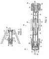
- a hand-held systemincludes a bipolar x-ray tube 300 within a housing 302, and a bipolar high voltage power supply within a different housing 304.
- the bipolar high voltage power supplyincludes a step-up transformer 306 coupled to a positive high voltage multiplier 308, and another step-up transformer 310 coupled to a negative high voltage multiplier 312.
- the positive high voltage multiplier 308provides the positive high voltage via cables 316 to an anode 318 of the bipolar x-ray tube 300, while the negative high voltage multiplier 312 provides the negative high voltage via cables 320 to a cathode 322 of the bipolar x-ray tube 322.
- the cathode emitter voltage(with respect to the cathode high voltage) is provided by the isolation transformer 314 via cables 324 to an electron emitter within the cathode 322.
- the bipolar x-ray tube 300may preferably operate at an electron beam power of less than about 10 Watts, and more preferably may operate at an electron beam power of between about 1 Watt and about 5 Watts.
- An optional intermediate electrode 326may be included between ceramic insulators 327 and 328, and may be coupled to a system reference ground.
- the system of Figure 12permits the bipolar x-ray tube to be decoupled from the bipolar high voltage power supply. Power may be provided to the high voltage power supply within the housing 304 by a battery, alternating currently supply, portable generator, solar cell or other source of electricity together with a local oscillator, as is well known in the art.
- Figure 12shows a top view of a lower halves of housings 302 and 304 containing the tube and voltage supply respectively, with the top halves of the housings removed. The housings 302 and 304 may be packaged within a further device housing in a hand-held x-ray instrument.
- a bipolar x-ray tube 350may be provided in a hand-held system, in which the x-ray tube 350 includes in a vacuum environment, an electrically insulating wall 369,an anode 352, a cathode 354, and an x-ray transmissive output window 356.
- the cathode 354includes a cathode shroud 358 coupled to a negative high voltage potential, and a cathode electron emitter 360 which may be heated.
- the anode 352includes a positive high voltage electrode 362 coupled to a positive high voltage potential.
- a solid target 366is provided in the path of the electron beam such that a portion of the x-rays are emitted may pass through the x-ray transmissive window 356 that is formed into a housing 368.
- the x-ray transmissive window 356may be provided at reference ground potential.
- Figure 14shows a bipolar x-ray tube 400 that may be provided in a hand-held system, in which the x-ray tube 400 includes in a vacuum environment, an electrically insulating wall 419, an anode 402, a cathode 404, and an x-ray transmissive output window 406.
- the cathode 404includes a cathode shroud 408 coupled to a negative high voltage potential, and a cathode electron emitter 410 which may be heated.
- the anode 402includes a positive high voltage electrode 412 coupled to a positive high voltage potential.
- a solid target 416is provided in the path of the electron beam such that x-rays are emitted and may pass through the x-ray transmissive window 406 that is formed into a housing 418.
- the x-ray transmissive window 406may be provided at reference ground potential.
- the anode and the cathodedirectly oppose one another, and in both of the x-ray tubes of Figures 13 and 14 , the difference between the negative high voltage potential and the positive high voltage potential is employed to cause electrons to be directed toward the x-ray producing target.
- the bipolar x-ray tubes of Figures 13 and 14may each be encapsulated in x-ray shielding and voltage insulating potting material as discussed above.
- the bipolar x-ray tubes 350 and 400may each preferably operate at less than about 10 Watts, and more preferably may operate between about 1 Watt and 5 Watts.
- the solid target materials 366 and 416may each include silver, gold, tungsten, rhenium or other metals, and the x-ray transmissive window materials 356 and 406 may each include beryllium, beryllium oxide, aluminum and other light materials.
- the positive high voltage potential and the negative high voltage potentialmay be provided as discussed above, employing step up transformers and voltage multipliers.
- the power sourcemay be provided by battery or an alternating currently supply, together with a local oscillator as is well known in the art.
- the housing 368 and 418 of the x-ray tubes of Figures 13 and 14may be packaged within a further device housing in a hand-held x-ray instrument.
Landscapes
- X-Ray Techniques (AREA)
- Analysing Materials By The Use Of Radiation (AREA)
Description
- The present invention relates to systems and methods for providing compact X-ray sources for use in field portable or hand-held x-ray analytical instruments, and relates in particular to the design and construction of low power high voltage x-ray sources for use in field portable or hand-held x-ray analytical instruments.
- Interest in the measurement of material properties using x-ray techniques has resulted in the development of compact, low power consumption x-ray sources for portable x-ray analytical instruments. Examples of such instruments are the hand-held x-ray fluorescence analyzers currently available from companies such as ThermoFisher Scientific Inc., Niton Analyzers, of Billerica, Massachusetts, , InnovX Systems of Woburn, Massachusetts, and Oxford Instruments Company of Oxon, United Kingdom. In such conventional systems, however, the voltages of the x-ray sources have been generally limited because of the size requirements for the x-ray tube and the high voltage power supply, as well as the associated electrical insulation and radiation shielding requirements.
- For example, as shown in
Figure 1 , a portion of a conventional hand-held x-ray source may include anx-ray tube 10 within ahousing 12 such that x-rays may be emitted by the x-ray tube through anx-ray output region 14 of thehousing 12. The x-ray tube includes ananode end 16, a cathode end 18, andintermediate section 20 between theanode end 16 and the cathode end 18. Theanode end 16 of thex-ray tube 10 includes ananode hood 22, anx-ray producing target 24, and an x-raytransmissive window 26. The cathode end 18 includes a cathode shroud 28, anelectron emitter 34, andelectrical connections electron emitter 34. Theintermediate section 20 may be formed of an electrical insulator such as ceramic or glass. The electrical insulator is sealed to the anode and cathode ends of the x-ray tube, thereby producing a interior region of the x-ray tube in which a vacuum can be produced and maintained. - During use, heater power is supplied to the
cathode electron emitter 34, and a high voltage (e.g., 30-50 kV) is applied between the cathode end 18 and theanode end 16. The electric field produced by the applied high voltage accelerates electrons from the electron emitter through the vacuum to thex-ray producing target 24. The intensity of the x-rays produced at the target increases with increasing high voltage, electron beam current, and atomic weight of the target material. A portion of the x-rays produced in the target exit the tube via thex-ray transmission window 26, and exit thehousing 12 via thex-ray output region 14 of thehousing 12. The high voltage at the cathode end is typically provided as a negative high voltage (e.g., -50 kV) and the voltage potential at the anode end is typically provided at a reference ground potential of the system. This permits theanode end 16 of thetube 10 to be coupled directly to thehousing 12. Thex-ray tube 10 may be packaged in a hand held device that includes a high voltage power supply and a power source to drive the electron emitter. - For fixed values of the high voltage and electron current, the intensity of the x-rays at a location outside the x-ray tube decreases rapidly with increasing distance to the x-ray producing target. The x-ray intensity may be further reduced by the presence of intervening materials that scatter or absorb x-rays. Therefore, in order to maximize x-ray intensity at a given location, it is advantageous to minimize the distance from a sample or detector to the x-ray producing target and to eliminate to the extent possible any materials that scatter or absorb x-rays from the x-ray path. For these reasons, the x-ray producing target is placed as close as possible to the x-ray transmission window, and the x-ray transmission window is generally provided at an exterior surface of the housing at the output region. For example, the x-ray producing target and x-ray transmission window may be provided at a protruding portion or nose of a hand-held device, a portion of an example of which is shown in at 12
Figure 1 . - The accurate identification and quantification of elements at depths within certain materials, as well as the identification of certain heavy elements (e.g., lead and cadmium), generally requires the use of higher voltage sources (e.g., 80 to 150 kV) for x-ray production. Increasing the voltage level of the high voltage, however, generally requires that the length and diameter of the x-ray tube be increased in order to provide sufficient high voltage insulation between the anode and cathode conductors inside the vacuum envelope of the x-ray tube. Increased x-ray tube size therefore, requires an increase in the size of the hand-held x-ray inspection device. Further, providing sufficient electrical insulation between the housing and electrodes at significantly higher voltages also requires larger distances and thicker insulation. The doubling of the voltage level of a 50 kV tube, therefore, requires a substantial increase in size of a hand-held device that includes the higher voltage x-ray tube.
- There remains a need, therefore, for a high voltage hand-held x-ray inspection device that is small - scale (uses a miniature x-ray source), yet is capable of operating in the range of approximately up to, for example, 150 kV.
US 2 871 402 discloses a high voltage electron tube that includes a cathode, an anode and metallic sleeves through which the electron beam passes from the cathode to the anode. Each of the metallic sleeves is connected to ground via a resistor(through which no substantial current flows in order to decrease the chance of "arc-over" between the cathode and the anode.US 2007/121788 concerns a modular X-ray tube and method for the production of such an X-ray tube, in which an anode and a cathode are arranged in a vacuumized inner space situated opposite each other, electrons being produced at the cathode and X-rays at the anode. The X-ray tube comprises a multiplicity of acceleration modules, complementing one another, and each acceleration module comprises at least one potential-carrying acceleration electrode. A first acceleration module thereby comprises the cathode, a second acceleration module the anode. The X-ray tube further comprises at least one other acceleration module. In particular, the X-ray tube can possess a re-closeable vacuum valve, enabling individual defective parts of the tube to be replaced in a simple manner or enabling the tube to be modified in a modular way. The anode can comprise a target for x-ray generation with an emission hole, or can be designed as a transmission anode.EP 0 488 991 describes a method and apparatus for the production of fluoroscopic and radiographic x-ray images utilizing a portable hand-held and battery operated x-ray system. The system incorporates a unique high voltage power supply of diminutive size and weight which may be disposed totally within the hand-held system. By utilizing the system in conjunction with a currently available hand operated instant Polaroid film developer, the system provides total portability and field operability in both fluoroscopic and radiographic mode.EP 0 924 742 discloses an x-ray tube that includes an envelope defining an evacuated chamber and having a window transmissive to x-rays. An anode assembly and a cathode assembly operate within the envelope to produce x-rays which travel through the window transmissive to x-rays towards a patient or subject under examination. A shield transmissive to x-rays is coupled to the envelope and positioned such that x-rays travelling through the window transmissive to x-rays must first travel through the shield. The shield prevents substantially all secondary electrons created during the production of x-rays from coming into contact with the window transmissive to x-rays thereby preventing excessive heating of the window transmissive to x-rays. An electrode defined by the envelope in a region proximate the window transmissive to x-rays may additionally or alternatively be used to prevent secondary electrons from reaching the window transmissive to x-rays.- The invention provides an x-ray system according to
claim 1. - Prefered embodiments are defined in the dependent claims.
- The following description may be further understood with reference to the accompanying drawings in which:
Figure 1 shows an illustrative diagrammatic sectional side view of a conventional x-ray tube;Figure 2 shows an illustrative diagrammatic sectional side view of a bipolar x-ray tube having a transmission end-window;Figure 3 shows an illustrative diagrammatic view of electrical components in a hand-held x-ray source system;Figure 4 shows an illustrative diagrammatic plan view of physical components in a hand-held x-ray system;Figure 5 shows an illustrative diagrammatic isometric view partial view of an anode end of a bipolar x-ray tube within a housing;Figure 6 shows an illustrative diagrammatic isometric view partial view of an anode end of a bipolar x-ray tube within a housing;Figures 7A - 7C show illustrative diagrammatic sectional views of output transmission interfaces between housings and anode ends of a bipolar x-ray tubes in examples useful for understanding the invention and embodiments of the invention;Figure 8 shows an illustrative diagrammatic plan view of physical components in a hand-held x-ray source;Figure 9 shows an illustrative diagrammatic sectional side view of a bipolar x-ray tube having a side window;Figure 10 shows an illustrative diagrammatic plan view of physical components in a hand-held x-ray source;Figure 11 shows a partial sectional side view of the hand-held x-ray source shown inFigure 11 taken along line 11 - 11 thereof;Figure 12 shows an illustrative diagrammatic plan view of physical components in a hand-held x-ray source;Figure 13 shows an illustrative diagrammatic sectional view of a bipolar x-ray tube within a housing in a hand-held x-ray system ; andFigure 14 shows an illustrative diagrammatic sectional view of a bipolar x-ray tube within a housing in a hand-held x-ray system.- The drawings are shown for illustrative purposes only, and are not to scale.
- It has been discovered that a bipolar x-ray tube may be used in hand-held x-ray systems. Electrically insulating the high voltages of an x-ray tube from the typically grounded housing of hand-held x-ray sources is commonly achieved by maintaining the cathode at a negative high voltage potential within an electrically insulated portion of a source housing, while the anode (typically at system ground reference potential) is adjacent an output region of the housing.
- Although bi-polar x-ray tubes generally use a positive high voltage potential in addition to a negative high voltage potential, it has been found that the high voltage potentials of a bipolar x-ray tube may be sufficiently electrically insulated within a hand-held source yet also produce sufficient output of x-rays through an x-ray output region of the device, and provide significantly higher x-ray energies than are possible with single polarity x-ray tubes
- As shown, in
Figure 2 , a transmission end-windowbipolar x-ray tube 50 includes acathode 52, ananode 54, anintermediate electrode 56, and twoinsulators intermediate electrode 56. A vacuum is produced within the tube using a vacuum pump, and the tube is then sealed by closing off the pinch-offtube 74. The x-ray tube is maintained under vacuum after pinch-off using avacuum getter 72. Thecathode 52 includes an electron emitter 62 (such as a tungsten filament, a thoriated tungsten filament, an oxide-coated material, or other material with a low work function) across which a small potential may be applied via connectingpins cathode 52 is maintained at a negative high voltage potential and includes acathode shroud 68 and a negative high voltage shield 70 (such as tungsten, stainless steel, copper, brass or lead). Other electron sources may be employed at the cathode that are caused to emit electrons using other means such as photoemitters, field emitters, and cold emitters such as carbon nanotubes. - Within the vacuum, electrons are emitted along a
path 76 and pass through anintermediate shroud 78 of theintermediate electrode 56. Theintermediate electrode 56 also includes anintermediate conductor 80 as well as anintermediate shield 82, which may be formed of a material such as tungsten, stainless steel, copper, lead or brass. - The
anode 54 is maintained at a positive high voltage potential, and includes anx-ray producing target 84 within ananode hood 86, and anx-ray transmission window 88. Theanode 54 also includes a positivehigh voltage shield 90 formed, for example, of tungsten, stainless steel, copper, brass, or lead. - The miniature bipolar x-ray tube may be, for example, between about 2 to 4 inches in length (from the pinch-off
tube 74 to the far end of the anode 54), and the tube itself may be about 0.2 to about 0.5 inches in diameter, and is preferably about 0.3 inches in diameter as shown at A inFigure 2 . Because the system employs a negative high voltage potential and a positive high voltage potential, the difference between any individual component and ground reference is at most the greater of the two potentials. For example, if the cathode is maintained at - 50 kV, and the cathode is maintained at + 50 kV, then the difference between any component in the system with respect to ground reference is only 50 kV. Thebipolar x-ray tube 50 may preferably operate at an electron beam power of less than about 10 Watts, and more preferably may operate at an electron beam power of between about 0.1 Watt and about 5 Watts. - The intermediate electrode may be maintained at a voltage substantially half-way between the cathode and anode potentials, e.g., ground reference potential. As discussed in more detail below, this disclosure further provides a bipolar high voltage power supply connected to the x-ray tube, and that the x-ray tube, power supply and connection means are encapsulated in an electrically insulating material and enclosed in an electrically conducting sheath maintained at substantially ground reference potential. In certain embodiments, selected regions of the electrically insulating material may also contain x-ray shielding material.
- The x-ray tube of
Figure 2 uses a linear (as opposed to radial) insulator design that allows the diameter of the tube to be kept small. Small tube diameter in the vicinity of the x-ray window is advantageous in that it allows the x-ray source to be placed in close proximity to the sample being irradiated by the x-ray flux. Two cylindrical linear insulators separate the cathode and anode conductors, respectively, from the intermediate conductor. The insulators and the cathode, anode and intermediate electrode form the vacuum envelope of the tube. - The electron beam is generated by the electron emitter at cathode potential and accelerated to the x-ray emitting target at anode potential. In traversing the region between the cathode and anode conductors, the electron beam passes through the intermediate electrode, which is maintained at local reference ground potential. The total beam energy when it reaches the anode is the electron charge e multiplied by the total voltage change from the cathode to the anode. In
Figure 2 , the magnitudes of the cathode and anode potentials are equal, and opposite in polarity, e.g., they may be both 50 kV in magnitude, with the cathode at - 50 kV and the cathode at + 50 kV. It may be advantageous to operate the tube with different magnitudes of the cathode and anode potentials while still maintaining a desired beam energy. Using different potentials on these electrodes may alter the electron beam optics in the tube and may permit focusing or defocusing of the electron beam compared with the equal potential case. - The
intermediate electrode 56 provides a benefit that the positive and negative regions of the tube are decoupled along the external and internal surfaces of the insulator, thereby reducing the probability of a full voltage arc along the insulated length of the tube. The positive and negative triple points where the two insulators join theintermediate conductor 80 are shielded by theintermediate shield 82 on the outside of the tube and by theintermediate shroud 78 on the vacuum side. Similarly, the triple points where theinsulator sections cathode shroud 68 andanode hood 86 on the vacuum side. - The
intermediate shield 82 and the negative and positive high voltage shields 70 and 90 respectively may also provide additional x-ray shielding in the radial direction. The negativehigh voltage shield 70 may also provide x-ray shielding in the backwards axial direction, and the positivehigh voltage shield 90 may provide collimation of the x-ray beam in the forward axial direction. For this reason, the intermediate, negative, and positive shields may be made from a high atomic weight material such as tungsten, copper, brass, lead or other heavy metals. - The
intermediate shroud 78 is configured as a conducting tube with apertures at either end. The length and diameter of the tube and apertures are chosen so as to provide a clear path for the accelerated electron beam while also helping to prevent stray ions or electrons produced in one half of the x-ray tube from reaching the other half. If the length of the intermediate conductor is significantly longer than its diameter, the region inside the conductor will be a region of low electric field and stray particles with large transverse velocity relative to their velocity along the axis of the tube will be collected on the walls of the tube with high probability. In this way, for example, secondary ions formed in the region of the x-ray tube surrounded byinsulator 60 will be impeded from reaching the region of the x-ray tube surrounded byinsulator 58, and secondary electrons produced in the latter region will be impeded from traveling to the former. This internal configuration helps to prevent the formation of discharges within the vacuum envelope. - Electrons produced at the cathode emitter travel trough the
intermediate shroud 78 to thex-ray producing target 84. The target is a thin coating of a selected material applied to the surface of the x-ray window. A portion of the x-rays produced in the target coating pass through thewindow 88 in the forward direction. Coating materials may include silver, gold, tungsten, rhenium or other metals and x-ray window materials may include beryllium, beryllium oxide, aluminum and other light materials. Theanode hood 86 serves to prevent x-rays and stray electrons or ions from reaching the insulator surface and initiating high voltage breakdown. - With reference to
Figure 3 , apower supply oscillator 100, which may be either provided by an external oscillator via a cable or an internal oscillator system, and may be battery powered or powered from a cable, provides an oscillating signal to a first step-uptransformer 102 that is coupled to afirst voltage multiplier 104, and provides an oscillating signal to a second step-uptransformer 106 that is coupled to asecond voltage multiplier 108. A small voltage is also applied to anisolation transformer 110, the output of which will be used to heat the cathode emitter, 120, and produce electron emission from the cathode, 118. The output of thefirst voltage multiplier 104 is a positive high voltage potential (e.g., + 20 kV to + 70 kV) and is provided via aseries resistor 112 to ananode 114 of a bipolar x-ray tube. The output of thesecond voltage multiplier 108 is a negative high voltage potential (e.g., - 20 kV to - 70 kV) and is provided via aseries resistor 116 to acathode 120 of a bipolar x-ray tube. Thecathode 118 includes theelectron emitter 120, and one side of theelectron emitter 120 is coupled to the negative high voltage potential. An optional intermediate node is coupled to ground reference potential. - A feedback circuit may also be provided that maintains the positive and negative high voltage potentials at the desired levels, and the feedback circuit may include a voltage divider
circuit including resistors resistors 128, 131 for the negative high voltage output, each of which is coupled to a feedback controller as shown at 132. A feedback circuit may also be included (not shown) for stabilizing the electron beam current collected at the anode as is well known in the art. - The bipolar high voltage DC power supply therefore comprises two independently-controlled high frequency voltage multiplier circuits, each configured to reach a voltage corresponding to approximately half of the final electron beam energy in the x-ray tube. Examples of such multiplier circuits are cascade multipliers or Cockroft Walton voltage multipliers. A filament isolation transformer provides power to electron emitter, which may be a high temperature filament, or an oxide-coated or dispenser cathode. X-ray tube current is measured using a current sense resistor and high voltage is measured using a voltage divider resistor. In certain embodiments, an insulating encapsulant may surround the high voltage power supply, and the encapsulant may not contain x-ray shielding material, except in the regions adjacent to the bipolar x-ray tube. In other embodiments the high voltage insulation may be provided by an insulating liquid such as Fluorinert or oil.
Figure 4 shows a hand-held x-ray system that includes a bipolar x-ray tube including theanode 114, theintermediate electrode 122 and thecathode 118. The system also includes the first step-uptransformer 102 and thefirst voltage multiplier 104, as well as the second step-uptransformer 106 and thesecond voltage multiplier 108. The system further includes the highvoltage isolation transformer 110 as well as awall 124 at ground reference potential separating at least a portion of thefirst voltage multiplier 104 from thesecond voltage multiplier 108. The groundedwall 124 is also coupled to theintermediate electrode 122 as shown to contribute to electrical isolation of the positive high voltage potential from the negative high voltage potential.- The outputs of the
voltage multipliers cathode electrodes series resistors voltage multipliers housing 126 and the components therein via apower cable 128. Power may be provided by a battery, alternating currently supply, portable generator, solar cell or other source of electricity together with a local oscillator (not shown inFigure 4 ) as is well known in the art. Figure 4 shows a top view of a lower half of a housing containing the tube and voltage supply with a top half of the housing removed. Theinterior region 129 of thehousing 126 may be filled with air, but is preferably filled with an electrically insulating material in order to minimize the distance required between the internal components at high voltage and thehousing 126 at reference ground potential. Theinterior region 129 provides a passive cooling system that permits the x-ray tube to be sufficiently cooled during use. Examples of materials that may be used in theregion 129 are solid encapsulants such as silicone rubber or epoxy, liquids such as Fluorinert or oil, or insulating gases such as sulfer hexafluoride. Thex-ray source housing 126 may be packaged, along with other components, within the housing of a hand-held x-ray instrument, such as an x-ray fluorescence materials analyzer, lead detector, x-ray imaging system, or medical therapy device.- As further shown in
Figure 5 , an x-ray output region, such as anaperture 130 of thehousing 126, is aligned with anx-ray transmissive window 132 of the bipolar x-ray tube such that x-rays emitted through thex-ray transmissive window 132 exit the housing via thex-ray output aperture 130 of thehousing 126. The positivehigh voltage multiplier 104 and associatedseries resistor 112 are also shown inFigure 4 , as well as theintermediate node 122 coupled to the groundedwall 124. - The region between the
x-ray output aperture 130 and thex-ray transmissive window 132 must provide electrical insulation between theanode 114 at the positive high voltage potential an thehousing 126 at the reference ground potential while being highly transparent to the x-rays emitted through thex-ray transmissive window 132. As shown, for example inFigure 6 , the x-ray output interface may include a different material orcomponent 134 that provides electrical insulation of the anode, which is at the positive high voltage potential, yet also provides that x-rays are freely transmitted through the material or component as shown inFigure 6 . The remaining components ofFigure 6 are the same as those ofFigure 5 . - For example,
Figures 7A and 7C show certain examples useful for understanding the invention of x-ray output interfaces that may be employed. InFigure 7A , thematerial 134 is provided as an electrically insulating, x-ray transmissive solid potting material such as, for example, RTV, silicone rubber, epoxy, and urethane. The output transmission interface is provided between thex-ray transmissive window 88, through an opening in the anodehigh voltage shield 90, and extends to theoutput aperture 130 of thehousing 126. Asolid potting material 136 is provided around the remaining portions of the x-ray tube. Thepotting material 136 provides a passive cooling system that permits the x-ray tube to be sufficiently cooled during use. Thepotting material 136 is also electrically insulating and x-ray absorbing to provide radiation shielding from x-rays emanating from the x-ray tube through surfaces other that thex-ray transmissive window 88 Such materials include RTV, silicone rubber, epoxy and urethane potting materials impregnated with shielding materials such as lead, lead oxide, bismuth oxide, tungsten powder, and tungsten oxide. - As shown in
Figure 7B , for embodiments of the present invention, the output transmission interface employs a sealedtube 138 that provides avacuum 140 within thetube 138. Alternately, thevacuum region 140 may also be connected directly into an evacuated region of the x-ray tube assembly. - As shown in
Figure 7C , the size of the opening in thex-ray output aperture 130 may be smaller than the diameter of thex-ray transmissive window 88.Figure 7C shows an x-rayflux shaper element 142 that provides a smaller diameter x-ray beam. In other embodiments, thefield shaper element 142 may have other shapes and opening sizes to provide collimation or shaping of the x-ray flux.. The remaining portions of the output transmission interfaces ofFigures 7B and 7C are similar to those discussed above. - As shown in
Figure 8 , the disclosure provides ahousing 148 for abipolar x-ray tube 150 and a bipolar voltage source that includes first step-uptransformer 152 coupled to a positivehigh voltage multiplier 154, and a second step uptransformer 156 coupled to a negativehigh voltage multiplier 158. The voltage source is provided by battery or an alternating currently supply, together with a local oscillator (not shown inFigure 8 ) as is well known in the art. The system also includes anisolation transformer 160, and the positive high voltage potential is applied to ananode 162 of abipolar x-ray tube 150, while the negative high voltage potential is applied to acathode 164 of thex-ray tube 150 as discussed above. Thebipolar x-ray tube 150 may preferably operate at an electron beam power of less than about 10 Watts, and more preferably may operate between about 1 Watt and 5 Watts. Thehousing 126 may also be packaged within a further device housing in a hand-held x-ray instrument. - The system also includes two
insulators intermediate electrode 170 that is coupled to a system reference ground. The system ofFigure 8 also includes an x-ray transmissive electrically insulatingpotting material 172 between the x-ray transmissive window of the bipolar x-ray tube and the output region of the housing. The system further includes an electrically insulating encapsulatingmaterial 174 that contains x-ray shielding material surrounding thebipolar x-ray tube 150, and an electrically insulatingmaterial 176 that does not contain x-ray shielding material surrounding the bipolar high voltage supply. The encapsulatingmaterial 174 as discussed above that provides a passive cooling system that permits the x-ray tube to be sufficiently cooled during use. - In
Figure 8 , therefore, the x-ray tube, power supply, and connection means are encapsulated in solid electrically insulating encapsulant. Preferred encapsulating materials include silicone rubbers and epoxies. The x-ray tube and power supply components are positioned so as to minimize the required distance between components and thickness and total quantity of insulating material surrounding the components. The portion of the electrically insulating material adjacent to the x-ray tube contains x-ray shielding material distributed within. The x-ray shielding material and concentration is selected so as not to compromise the electrically insulating properties of the encapsulant. Preferred shielding materials include oxides of bismuth, tungsten and other heavy metals in fine powder form. The electrically insulating material in regions away from the x-ray tube do not contain x-ray shielding material in order to reduce the weight and cost of the device. - The
x-ray transmission interface 172 may be filled with encapsulating material that is left free from x-ray shielding material, thus allowing the x-rays to pass to the outside of the module with minimal attenuation and scattering. The thickness of this region is kept as small as possible to permit efficient transmission of x-rays. This thickness is typically less than 0.5 inches thick and preferably between 0.1 and 0.3 inches thick. This shielding-free channel provides collimation of the x-ray beam, and the shape of this region may be chosen to provide the desired x-ray beam spatial profile as discussed above with reference toFigures 6 and7A and 7C or, for embodiments,Figure 7B . If attenuation and scattering of the x-ray beam in the encapsulant material is an issue, thex-ray transmission interface 172 between the x-ray tube window and the outer surface of the encapsulant may be filled with sulfur hexafluoride gas, either pressurized or at atmospheric pressure. Sulfur hexafluoride gas is preferred for certain applications because it is an excellent electrical insulator and because its high molecular weight makes it easy to contain in a sealed cavity. - As shown in
Figure 9 , a system may include a side-windowbipolar x-ray tube 200 that includes ananode 202, acathode 204, an optionalintermediate electrode 206, and twoinsulators intermediate electrode 206. Thecathode 204 includes a cathode electron emitter 212 (such as tungsten, thoriated tungsten, an oxide, or tantalum) across which a small potential may be applied via connectingpins cathode 204 is maintained at a negative high voltage potential and includes acathode shroud 218 and a negative high voltage shield 220 (made from a material such as tungsten, stainless steel, copper, brass, or lead). A vacuum is obtained within the tube by evacuating and closing off the tube at the pinch-offtube 224, and is maintained in the tube using avacuum getter 222,. Thebipolar x-ray tube 200 may preferably operate at an electron beam power of less than about 10 Watts, and more preferably may operate at an electron beam power of between about 1 Watt and about 5 Watts. - Within the vacuum, electrons are emitted along a
path 226 and pass through anintermediate shroud 228 of theintermediate electrode 206. Theintermediate electrode 206 also includes anintermediate conductor 230 as well as anintermediate shield 232, which may be formed of a high atomic weight material such as tungsten, stainless steel, copper, brass, lead or other heavy metal. - The
anode 202 is maintained at a positive high voltage potential, and includes anx-ray producing target 234 within ananode hood 236 and anx-ray transmission window 238. Theanode 202 also includes a positivehigh voltage shield 240 formed, for example, of a tungsten, stainless steel, copper, brass, or lead. - The miniature bipolar x-ray tube may be, for example, between about 2 to 4 inches in length (from the pinch-off
tube 224 to the far end of the anode 202), and the tube itself may be about 0.2 to about 0.5 inches in diameter, and is preferably about 0.3 inches in diameter as shown at B inFigure 9 . Again, because the system employs a negative high voltage potential and a positive high voltage potential, the difference between any individual component and ground reference is at most the greater of the two potentials. For example, if the cathode is maintained at - 50 kV, and the cathode is maintained at + 50 kV, then the difference between any component in the system with respect to ground is only 50 kV. The intermediate electrode may be maintained at a voltage substantially half-way between the cathode and anode potentials, e.g., ground potential. - As further shown in
Figures 10 and 11 , thebipolar x-ray tube 200 may be provided within ahousing 250 that also includes a bipolar high voltage supply. In particular, a step-uptransformer 252 is coupled to a positivehigh voltage multiplier 254, and another step-uptransformer 256 is coupled to a negativehigh voltage multiplier 258. Anisolation transformer 260 provides a small voltage potential to theelectron emitter 212 in the cathode via connectingpins - Similar to
Figure 2 , the electron beam is generated by the electron emitter at cathode potential and accelerated to the x-ray emitting target at anode potential. In traversing the region between the cathode and anode conductors, the electron beam passes through the intermediate electrode, which is maintained at local reference ground potential. The total beam energy when it reaches the anode is the electron charge e multiplied by the total voltage change from the cathode to the electrode. In the x-ray tube shown inFigure 9 , the magnitudes of the cathode and anode potentials are equal, and opposite in polarity, but it may be advantageous to operate the tube with different magnitudes of the cathode and anode potentials while still maintaining a desired beam energy as discussed above with reference toFigure 2 . - Electrons produced at the
cathode emitter 212 travel through theintermediate shroud 230 to thex-ray producing target 234. The x-ray producing target may be a solid piece of target material or a thin layer of target material applied to a substrate and disposed at an angle to the direction of the electron beam path. A portion of the x-rays produced in thetarget 234 impinge on thex-ray transmissive window 238. The portion of the x-rays that reach thewindow 238 are passed out of the bipolar x-ray tube through an x-rayoutput transmission interface 262 disposed between thex-ray transmissive window 238 and the housing 250 (shown inFigure 11 ). Thex-ray transmissive interface 262 may be configured as discussed previously and shown inFigures 6 ,7A-C , and8 . The x-ray producing target material may include silver, gold, tungsten, rhenium or other metals, and the x-ray transmissive window materials may include beryllium, beryllium oxide, aluminum and other light materials. Theanode hood 236 serves to prevent x-rays and stray electrons or ions from reaching the insulator surface and initiating high voltage breakdown. - In
figure 12 a hand-held system includes abipolar x-ray tube 300 within ahousing 302, and a bipolar high voltage power supply within adifferent housing 304. The bipolar high voltage power supply includes a step-uptransformer 306 coupled to a positivehigh voltage multiplier 308, and another step-uptransformer 310 coupled to a negativehigh voltage multiplier 312. The positivehigh voltage multiplier 308 provides the positive high voltage viacables 316 to ananode 318 of thebipolar x-ray tube 300, while the negativehigh voltage multiplier 312 provides the negative high voltage viacables 320 to acathode 322 of thebipolar x-ray tube 322. The cathode emitter voltage (with respect to the cathode high voltage) is provided by theisolation transformer 314 viacables 324 to an electron emitter within thecathode 322. Thebipolar x-ray tube 300 may preferably operate at an electron beam power of less than about 10 Watts, and more preferably may operate at an electron beam power of between about 1 Watt and about 5 Watts. - An optional
intermediate electrode 326 may be included betweenceramic insulators Figure 12 permits the bipolar x-ray tube to be decoupled from the bipolar high voltage power supply. Power may be provided to the high voltage power supply within thehousing 304 by a battery, alternating currently supply, portable generator, solar cell or other source of electricity together with a local oscillator, as is well known in the art.Figure 12 shows a top view of a lower halves ofhousings housings - As shown in
Figure 13 , abipolar x-ray tube 350 may be provided in a hand-held system, in which thex-ray tube 350 includes in a vacuum environment, an electrically insulatingwall 369,ananode 352, acathode 354, and an x-raytransmissive output window 356. Thecathode 354 includes acathode shroud 358 coupled to a negative high voltage potential, and acathode electron emitter 360 which may be heated. Theanode 352 includes a positivehigh voltage electrode 362 coupled to a positive high voltage potential. Asolid target 366 is provided in the path of the electron beam such that a portion of the x-rays are emitted may pass through thex-ray transmissive window 356 that is formed into ahousing 368. Thex-ray transmissive window 356 may be provided at reference ground potential. Figure 14 shows abipolar x-ray tube 400 that may be provided in a hand-held system, in which thex-ray tube 400 includes in a vacuum environment, an electrically insulatingwall 419, ananode 402, acathode 404, and an x-raytransmissive output window 406. Thecathode 404 includes acathode shroud 408 coupled to a negative high voltage potential, and acathode electron emitter 410 which may be heated. Theanode 402 includes a positivehigh voltage electrode 412 coupled to a positive high voltage potential. Asolid target 416 is provided in the path of the electron beam such that x-rays are emitted and may pass through thex-ray transmissive window 406 that is formed into ahousing 418. Thex-ray transmissive window 406 may be provided at reference ground potential.- In the example of
Figure 14 , the anode and the cathode directly oppose one another, and in both of the x-ray tubes ofFigures 13 and 14 , the difference between the negative high voltage potential and the positive high voltage potential is employed to cause electrons to be directed toward the x-ray producing target. The bipolar x-ray tubes ofFigures 13 and 14 may each be encapsulated in x-ray shielding and voltage insulating potting material as discussed above. Thebipolar x-ray tubes solid target materials transmissive window materials - The positive high voltage potential and the negative high voltage potential may be provided as discussed above, employing step up transformers and voltage multipliers. The power source may be provided by battery or an alternating currently supply, together with a local oscillator as is well known in the art. The
housing Figures 13 and 14 may be packaged within a further device housing in a hand-held x-ray instrument. - Those skilled in the art will appreciate that numerous modifications and variations may be made to the above.
Claims (6)
- An x-ray system including a bipolar x-ray tube (50, 300) comprising two insulators (58, 60, 328, 166, 168, 327) that are separated by an intermediate electrode (56, 122, 170, 326), wherein each insulator forms a portion of an outer wall of a vacuum envelope of the bipolar x-ray tube surrounding at least a portion of a path (76) of an electron beam within the vacuum envelope, wherein said bipolar x-ray tube (50, 300) is further including an anode (54, 114, 162, 318) at a positive high voltage potential relative to a reference potential, a cathode (52, 118, 164, 322) at a negative high voltage potential relative to the reference potential, and an x-ray transmissive window (88, 132) at the positive high voltage potential, and wherein said x-ray transmissive window (88, 132) includes an x-ray producing target (84) on an inside surface thereof that is within the vacuum envelope, whereby said x-ray system comprises a housing (126) at the reference potential; and an insulating region between the x-ray transmissive window (88, 132) and the housing (126), wherein said insulating region is electrically insulating and transmissive to x-rays, and wherein said insulating region includes an evacuated region (140).
- The x-ray system as claimed in claim 1, wherein the intermediate electrode is at an intermediate potential that is between the positive high voltage potential and the negative high voltage potential.
- The x-ray system as claimed in claim 1, wherein each insulator is cylindrical in shape and is formed of ceramic, and wherein said intermediate electrode is at a potential that is a system reference ground.
- The x-ray system as claimed in claim 1, wherein said bipolar x-ray tube is configured to operate with an electron beam power of less than 10 Watts.
- The x-ray system as claimed in claim 1, wherein said housing (126) includes the bipolar power supply.
- The x-ray system as claimed in claim 5, wherein said bipolar power supply and the bipolar x-ray tube are enclosed in separate housings (302, 304) and are coupled together via coupling wires (316, 320, 324).
Applications Claiming Priority (2)
| Application Number | Priority Date | Filing Date | Title |
|---|---|---|---|
| US94811107P | 2007-07-05 | 2007-07-05 | |
| PCT/US2008/069195WO2009006592A2 (en) | 2007-07-05 | 2008-07-03 | Compact high voltage x-ray source system and method for x-ray inspection applications |
Publications (2)
| Publication Number | Publication Date |
|---|---|
| EP2179436A2 EP2179436A2 (en) | 2010-04-28 |
| EP2179436B1true EP2179436B1 (en) | 2014-01-01 |
Family
ID=39734105
Family Applications (1)
| Application Number | Title | Priority Date | Filing Date |
|---|---|---|---|
| EP08781355.6AActiveEP2179436B1 (en) | 2007-07-05 | 2008-07-03 | Compact high voltage x-ray source system and method for x-ray inspection applications |
Country Status (3)
| Country | Link |
|---|---|
| US (1) | US7949099B2 (en) |
| EP (1) | EP2179436B1 (en) |
| WO (1) | WO2009006592A2 (en) |
Families Citing this family (48)
| Publication number | Priority date | Publication date | Assignee | Title |
|---|---|---|---|---|
| DE102008038582A1 (en)* | 2008-08-21 | 2010-02-25 | Siemens Aktiengesellschaft | X-ray |
| EP2502236A4 (en) | 2009-11-16 | 2015-12-30 | Schlumberger Technology Bv | COMPACT RADIATION GENERATOR |
| US9793084B2 (en)* | 2009-11-16 | 2017-10-17 | Schlumberger Technology Corporation | Floating intermediate electrode configuration for downhole nuclear radiation generator |
| US9155185B2 (en)* | 2009-11-16 | 2015-10-06 | Schlumberger Technology Corporation | Electrode configuration for downhole nuclear radiation generator |
| JP2013530491A (en)* | 2010-05-07 | 2013-07-25 | コーニンクレッカ フィリップス エレクトロニクス エヌ ヴィ | Apparatus and method for generating x-rays using a mechanical energy source |
| EP2649634B1 (en)* | 2010-12-10 | 2018-07-04 | Canon Kabushiki Kaisha | Radiation generating apparatus and radiation imaging apparatus |
| JP5796990B2 (en)* | 2011-04-13 | 2015-10-21 | キヤノン株式会社 | X-ray generator and X-ray imaging apparatus using the same |
| JP5825892B2 (en) | 2011-07-11 | 2015-12-02 | キヤノン株式会社 | Radiation generator and radiation imaging apparatus using the same |
| JP2013020792A (en) | 2011-07-11 | 2013-01-31 | Canon Inc | Radiation generating device and radiography device using it |
| JP5791401B2 (en)* | 2011-07-11 | 2015-10-07 | キヤノン株式会社 | Radiation generator and radiation imaging apparatus using the same |
| KR101823876B1 (en)* | 2011-07-22 | 2018-01-31 | 한국전자통신연구원 | Layered x-ray tube apparatus using spacer |
| KR101818681B1 (en)* | 2011-07-25 | 2018-01-16 | 한국전자통신연구원 | Layered x-ray tube apparatus using spacer |
| JP5713832B2 (en)* | 2011-08-03 | 2015-05-07 | キヤノン株式会社 | Radiation generator and radiation imaging apparatus using the same |
| EP2740331B1 (en) | 2011-08-05 | 2018-05-30 | Canon Kabushiki Kaisha | Radiation generating apparatus and radiation imaging apparatus |
| JP6039282B2 (en)* | 2011-08-05 | 2016-12-07 | キヤノン株式会社 | Radiation generator and radiation imaging apparatus |
| JP5893350B2 (en)* | 2011-11-10 | 2016-03-23 | キヤノン株式会社 | Radiation tube and radiation generator using the same |
| ITVR20120035A1 (en)* | 2012-03-05 | 2012-06-04 | Roberto Molteni | COMPACT RADIOGRAPHICAL SOURCES FOR MODERATE LOADING USING RADIOGENOUS TUBE WITH CARBON NANOOTUBE CATODO. |
| JP6308714B2 (en)* | 2012-08-28 | 2018-04-11 | キヤノン株式会社 | Radiation generating tube and radiation generating apparatus provided with the radiation generating tube |
| US9072154B2 (en)* | 2012-12-21 | 2015-06-30 | Moxtek, Inc. | Grid voltage generation for x-ray tube |
| GB2517671A (en) | 2013-03-15 | 2015-03-04 | Nikon Metrology Nv | X-ray source, high-voltage generator, electron beam gun, rotary target assembly, rotary target and rotary vacuum seal |
| KR101400078B1 (en)* | 2013-04-15 | 2014-05-30 | (주)선재하이테크 | X X-ray generating device |
| WO2015034992A1 (en)* | 2013-09-04 | 2015-03-12 | Newton Scientific, Inc. | Transformer with highly resistive core |
| US9240303B2 (en)* | 2013-09-10 | 2016-01-19 | Moxtek, Inc. | Dual tube support for electron emitter |
| DE102014208345B4 (en)* | 2014-05-05 | 2021-07-29 | Siemens Healthcare Gmbh | X-ray device |
| TWI552187B (en)* | 2014-11-20 | 2016-10-01 | 能資國際股份有限公司 | Encapsulated structure for x-ray generator with cold cathode and method for vacuumed the same |
| KR102056081B1 (en) | 2015-06-30 | 2019-12-16 | 주식회사 바텍 | Portable X-ray generator having field emission X-ray source |
| DE102015213810B4 (en)* | 2015-07-22 | 2021-11-25 | Siemens Healthcare Gmbh | High voltage feed for an X-ray tube |
| JP6573380B2 (en) | 2015-07-27 | 2019-09-11 | キヤノン株式会社 | X-ray generator and X-ray imaging system |
| US10398011B2 (en) | 2015-11-12 | 2019-08-27 | Kimtron, Inc. | Method and apparatus for active filament management |
| US10342107B2 (en) | 2015-11-12 | 2019-07-02 | Kimtron, Inc. | Cascaded filament transformer within a resistive shroud |
| JP2019501493A (en)* | 2015-12-03 | 2019-01-17 | ヴァレックス イメージング コーポレイション | X-ray assembly |
| GB2545742A (en) | 2015-12-23 | 2017-06-28 | X-Tek Systems Ltd | Target assembly for an x-ray emission apparatus and x-ray emission apparatus |
| EP3420785B1 (en)* | 2016-02-26 | 2021-09-15 | Newton Scientific, Inc. | Bipolar x-ray module |
| JP6525941B2 (en) | 2016-10-28 | 2019-06-05 | キヤノン株式会社 | X-ray generator and X-ray imaging system |
| US10559446B2 (en)* | 2017-02-28 | 2020-02-11 | Electronics And Telecommunication Research Institute | Vacuum closed tube and X-ray source including the same |
| KR101966794B1 (en)* | 2017-07-12 | 2019-08-27 | (주)선재하이테크 | X-ray tube for improving electron focusing |
| US10616986B2 (en) | 2017-11-16 | 2020-04-07 | Moxtek, Inc. | Bipolar voltage multiplier with reduced voltage gradient |
| US10499484B2 (en)* | 2017-11-16 | 2019-12-03 | Moxtek, Inc. | X-ray source with non-planar voltage multiplier |
| US10748740B2 (en)* | 2018-08-21 | 2020-08-18 | Fei Company | X-ray and particle shield for improved vacuum conductivity |
| US10825634B2 (en)* | 2019-02-21 | 2020-11-03 | Varex Imaging Corporation | X-ray tube emitter |
| JP7337577B2 (en)* | 2019-07-24 | 2023-09-04 | 浜松ホトニクス株式会社 | X-ray tube and X-ray generator |
| WO2021094642A1 (en)* | 2019-11-11 | 2021-05-20 | Ametek Finland Oy | A shield device for a radiation window, a radiation arrangement comprising the shield device, and a method for producing the shield device |
| US11683879B2 (en)* | 2020-06-09 | 2023-06-20 | Moxtek, Inc. | Scanning x-ray system |
| JP7577572B2 (en)* | 2021-03-03 | 2024-11-05 | 富士フイルム株式会社 | Radiation tubes and sources |
| US20220385163A1 (en)* | 2021-05-10 | 2022-12-01 | Marvin Bishop | Infinity Electrical Reactor (IER) Device |
| US12125661B2 (en) | 2021-07-28 | 2024-10-22 | Electronics And Telecommunications Research Institute | X-ray tube |
| US11972920B2 (en) | 2021-11-23 | 2024-04-30 | Fei Company | Vacuum compatible X-ray shield |
| EP4344357A1 (en)* | 2022-09-21 | 2024-03-27 | Comet AG | Electric field shaper, high-voltage generator device, x-ray generator and method for manufacturing an electric field shaper |
Citations (9)
| Publication number | Priority date | Publication date | Assignee | Title |
|---|---|---|---|---|
| GB818182A (en)* | 1955-05-18 | 1959-08-12 | Gen Electric | Improvements in targets for x-ray tubes |
| US3465154A (en)* | 1966-03-23 | 1969-09-02 | Philips Corp | High-voltage apparatus having an insulation of foamed material |
| US3812366A (en)* | 1971-03-08 | 1974-05-21 | Watkins Johnson Co | Composite x-ray tube/transformer assembly |
| US4157476A (en)* | 1978-02-03 | 1979-06-05 | General Electric Company | Dental X-ray tube head |
| US5303283A (en)* | 1991-09-03 | 1994-04-12 | General Electric Cgr S.A. | X-ray unit with high-voltage power supply device integrated into the casing |
| US6213639B1 (en)* | 1998-09-23 | 2001-04-10 | Siemens Aktiengesellschaft | Low-cost x-ray radiator |
| US20030185344A1 (en)* | 2000-05-12 | 2003-10-02 | Shimadzu Corporation | X-ray tube and X-ray generator |
| US6644853B1 (en)* | 2002-04-05 | 2003-11-11 | Arkady Kantor | X-ray tube head with improved x-ray shielding and electrical insulation |
| WO2005055270A1 (en)* | 2003-12-02 | 2005-06-16 | Comet Holding Ag | Modular x-ray tube and method for the production thereof |
Family Cites Families (15)
| Publication number | Priority date | Publication date | Assignee | Title |
|---|---|---|---|---|
| US2871402A (en)* | 1954-09-20 | 1959-01-27 | Westinghouse Electric Corp | Split section high voltage tube |
| EP0488991B1 (en)* | 1986-05-15 | 1995-09-20 | Xi Tec, Inc. | Method for production of fluoroscopic and radiographic X-ray images and hand held diagnostic apparatus incorporating the same |
| EP0780876A3 (en) | 1995-12-23 | 1997-12-10 | Philips Patentverwaltung GmbH | Drive device for a rotating anode of an x-ray tube |
| DE19830349A1 (en) | 1997-07-24 | 1999-01-28 | Siemens Ag | X=ray tube with magnetic deflection of electron beam |
| DE19743163C2 (en) | 1997-09-30 | 1999-11-11 | Siemens Ag | X-ray tube |
| US5978447A (en) | 1997-11-11 | 1999-11-02 | Picker International, Inc. | X-ray tube straddle bearing assembly |
| DE19752114A1 (en) | 1997-11-25 | 1999-05-27 | Philips Patentverwaltung | Drive device for an X-ray rotating anode and method for controlling the drive device |
| US6005918A (en)* | 1997-12-19 | 1999-12-21 | Picker International, Inc. | X-ray tube window heat shield |
| US20030210764A1 (en) | 2002-05-10 | 2003-11-13 | Tekletsadik Kasegn Dubale | Pulsed power application for x-ray tube |
| US6882703B2 (en) | 2002-07-31 | 2005-04-19 | Ge Medical Systems Global Technology Company, Llc | Electron source and cable for x-ray tubes |
| US7218707B2 (en)* | 2002-09-09 | 2007-05-15 | Comet Holding Ag | High-voltage vacuum tube |
| WO2005086203A1 (en) | 2004-03-02 | 2005-09-15 | Comet Holding Ag | X-ray tube for high dosing performances, method for producing high dosing performances with x-ray tubes and method for the production of corresponding x-ray devices |
| US7885386B2 (en) | 2006-03-31 | 2011-02-08 | General Electric Company | Systems and apparatus for a compact low power X-ray generator |
| US7495539B2 (en) | 2006-10-02 | 2009-02-24 | General Electric Company | Filament transformer for X-ray tubes |
| US20080095317A1 (en) | 2006-10-17 | 2008-04-24 | General Electric Company | Method and apparatus for focusing and deflecting the electron beam of an x-ray device |
- 2008
- 2008-07-03WOPCT/US2008/069195patent/WO2009006592A2/enactiveApplication Filing
- 2008-07-03USUS12/167,722patent/US7949099B2/enactiveActive
- 2008-07-03EPEP08781355.6Apatent/EP2179436B1/enactiveActive
Patent Citations (9)
| Publication number | Priority date | Publication date | Assignee | Title |
|---|---|---|---|---|
| GB818182A (en)* | 1955-05-18 | 1959-08-12 | Gen Electric | Improvements in targets for x-ray tubes |
| US3465154A (en)* | 1966-03-23 | 1969-09-02 | Philips Corp | High-voltage apparatus having an insulation of foamed material |
| US3812366A (en)* | 1971-03-08 | 1974-05-21 | Watkins Johnson Co | Composite x-ray tube/transformer assembly |
| US4157476A (en)* | 1978-02-03 | 1979-06-05 | General Electric Company | Dental X-ray tube head |
| US5303283A (en)* | 1991-09-03 | 1994-04-12 | General Electric Cgr S.A. | X-ray unit with high-voltage power supply device integrated into the casing |
| US6213639B1 (en)* | 1998-09-23 | 2001-04-10 | Siemens Aktiengesellschaft | Low-cost x-ray radiator |
| US20030185344A1 (en)* | 2000-05-12 | 2003-10-02 | Shimadzu Corporation | X-ray tube and X-ray generator |
| US6644853B1 (en)* | 2002-04-05 | 2003-11-11 | Arkady Kantor | X-ray tube head with improved x-ray shielding and electrical insulation |
| WO2005055270A1 (en)* | 2003-12-02 | 2005-06-16 | Comet Holding Ag | Modular x-ray tube and method for the production thereof |
Also Published As
| Publication number | Publication date |
|---|---|
| WO2009006592A2 (en) | 2009-01-08 |
| US20090010393A1 (en) | 2009-01-08 |
| EP2179436A2 (en) | 2010-04-28 |
| US7949099B2 (en) | 2011-05-24 |
| WO2009006592A3 (en) | 2009-03-26 |
Similar Documents
| Publication | Publication Date | Title |
|---|---|---|
| EP2179436B1 (en) | Compact high voltage x-ray source system and method for x-ray inspection applications | |
| US10880978B2 (en) | Bipolar X-ray module | |
| US9595415B2 (en) | X-ray generator and X-ray imaging apparatus | |
| US3714486A (en) | Field emission x-ray tube | |
| US6075839A (en) | Air cooled end-window metal-ceramic X-ray tube for lower power XRF applications | |
| EP2740331B1 (en) | Radiation generating apparatus and radiation imaging apparatus | |
| EP2547177B1 (en) | Radiation generating apparatus and radiation imaging apparatus | |
| CN103718653B (en) | Radiation Generating Device and Radiation Imaging Device | |
| JP5713832B2 (en) | Radiation generator and radiation imaging apparatus using the same | |
| US5384821A (en) | Radiogenic unit | |
| US8761345B2 (en) | X-ray tube | |
| US9603233B2 (en) | Particle accelerator with a heat pipe supporting components of a high voltage power supply | |
| US20030002627A1 (en) | Cold emitter x-ray tube incorporating a nanostructured carbon film electron emitter | |
| CA2781097C (en) | High voltage supply for compact radiation generator | |
| US4210813A (en) | Ionizing radiation generator | |
| EP2649635A1 (en) | Radiation generating apparatus and radiation imaging apparatus | |
| CN1334748A (en) | Electron Beam Multistage Accelerator Driven Probe Device | |
| US8792619B2 (en) | X-ray tube with semiconductor coating | |
| US9177753B2 (en) | Radiation generating tube and radiation generating apparatus using the same | |
| JP4829734B2 (en) | Ion mobility meter and ion mobility measuring method | |
| JPS6244449Y2 (en) | ||
| JP7073406B2 (en) | Small ionizing radiation source | |
| JP2020526866A (en) | Processes for manufacturing small sources for producing ionizing radiation, assemblies containing multiple sources and sources | |
| US8867706B2 (en) | Asymmetric x-ray tube | |
| JP5278895B2 (en) | Anode grounded X-ray tube equipment |
Legal Events
| Date | Code | Title | Description |
|---|---|---|---|
| PUAI | Public reference made under article 153(3) epc to a published international application that has entered the european phase | Free format text:ORIGINAL CODE: 0009012 | |
| 17P | Request for examination filed | Effective date:20100205 | |
| AK | Designated contracting states | Kind code of ref document:A2 Designated state(s):AT BE BG CH CY CZ DE DK EE ES FI FR GB GR HR HU IE IS IT LI LT LU LV MC MT NL NO PL PT RO SE SI SK TR | |
| AX | Request for extension of the european patent | Extension state:AL BA MK RS | |
| 17Q | First examination report despatched | Effective date:20100723 | |
| DAX | Request for extension of the european patent (deleted) | ||
| GRAP | Despatch of communication of intention to grant a patent | Free format text:ORIGINAL CODE: EPIDOSNIGR1 | |
| INTG | Intention to grant announced | Effective date:20130723 | |
| GRAS | Grant fee paid | Free format text:ORIGINAL CODE: EPIDOSNIGR3 | |
| GRAA | (expected) grant | Free format text:ORIGINAL CODE: 0009210 | |
| AK | Designated contracting states | Kind code of ref document:B1 Designated state(s):AT BE BG CH CY CZ DE DK EE ES FI FR GB GR HR HU IE IS IT LI LT LU LV MC MT NL NO PL PT RO SE SI SK TR | |
| REG | Reference to a national code | Ref country code:GB Ref legal event code:FG4D | |
| REG | Reference to a national code | Ref country code:CH Ref legal event code:EP | |
| REG | Reference to a national code | Ref country code:IE Ref legal event code:FG4D | |
| REG | Reference to a national code | Ref country code:DE Ref legal event code:R096 Ref document number:602008029655 Country of ref document:DE Effective date:20140213 | |
| REG | Reference to a national code | Ref country code:AT Ref legal event code:REF Ref document number:647913 Country of ref document:AT Kind code of ref document:T Effective date:20140215 | |
| REG | Reference to a national code | Ref country code:NL Ref legal event code:VDEP Effective date:20140101 | |
| REG | Reference to a national code | Ref country code:AT Ref legal event code:MK05 Ref document number:647913 Country of ref document:AT Kind code of ref document:T Effective date:20140101 | |
| REG | Reference to a national code | Ref country code:LT Ref legal event code:MG4D | |
| PG25 | Lapsed in a contracting state [announced via postgrant information from national office to epo] | Ref country code:IS Free format text:LAPSE BECAUSE OF FAILURE TO SUBMIT A TRANSLATION OF THE DESCRIPTION OR TO PAY THE FEE WITHIN THE PRESCRIBED TIME-LIMIT Effective date:20140501 Ref country code:LT Free format text:LAPSE BECAUSE OF FAILURE TO SUBMIT A TRANSLATION OF THE DESCRIPTION OR TO PAY THE FEE WITHIN THE PRESCRIBED TIME-LIMIT Effective date:20140101 | |
| PG25 | Lapsed in a contracting state [announced via postgrant information from national office to epo] | Ref country code:SE Free format text:LAPSE BECAUSE OF FAILURE TO SUBMIT A TRANSLATION OF THE DESCRIPTION OR TO PAY THE FEE WITHIN THE PRESCRIBED TIME-LIMIT Effective date:20140101 Ref country code:NL Free format text:LAPSE BECAUSE OF FAILURE TO SUBMIT A TRANSLATION OF THE DESCRIPTION OR TO PAY THE FEE WITHIN THE PRESCRIBED TIME-LIMIT Effective date:20140101 Ref country code:AT Free format text:LAPSE BECAUSE OF FAILURE TO SUBMIT A TRANSLATION OF THE DESCRIPTION OR TO PAY THE FEE WITHIN THE PRESCRIBED TIME-LIMIT Effective date:20140101 Ref country code:FI Free format text:LAPSE BECAUSE OF FAILURE TO SUBMIT A TRANSLATION OF THE DESCRIPTION OR TO PAY THE FEE WITHIN THE PRESCRIBED TIME-LIMIT Effective date:20140101 Ref country code:CY Free format text:LAPSE BECAUSE OF FAILURE TO SUBMIT A TRANSLATION OF THE DESCRIPTION OR TO PAY THE FEE WITHIN THE PRESCRIBED TIME-LIMIT Effective date:20140101 Ref country code:ES Free format text:LAPSE BECAUSE OF FAILURE TO SUBMIT A TRANSLATION OF THE DESCRIPTION OR TO PAY THE FEE WITHIN THE PRESCRIBED TIME-LIMIT Effective date:20140101 Ref country code:PT Free format text:LAPSE BECAUSE OF FAILURE TO SUBMIT A TRANSLATION OF THE DESCRIPTION OR TO PAY THE FEE WITHIN THE PRESCRIBED TIME-LIMIT Effective date:20140502 | |
| PG25 | Lapsed in a contracting state [announced via postgrant information from national office to epo] | Ref country code:BE Free format text:LAPSE BECAUSE OF FAILURE TO SUBMIT A TRANSLATION OF THE DESCRIPTION OR TO PAY THE FEE WITHIN THE PRESCRIBED TIME-LIMIT Effective date:20140101 Ref country code:HR Free format text:LAPSE BECAUSE OF FAILURE TO SUBMIT A TRANSLATION OF THE DESCRIPTION OR TO PAY THE FEE WITHIN THE PRESCRIBED TIME-LIMIT Effective date:20140101 Ref country code:LV Free format text:LAPSE BECAUSE OF FAILURE TO SUBMIT A TRANSLATION OF THE DESCRIPTION OR TO PAY THE FEE WITHIN THE PRESCRIBED TIME-LIMIT Effective date:20140101 | |
| REG | Reference to a national code | Ref country code:DE Ref legal event code:R097 Ref document number:602008029655 Country of ref document:DE | |
| PG25 | Lapsed in a contracting state [announced via postgrant information from national office to epo] | Ref country code:CZ Free format text:LAPSE BECAUSE OF FAILURE TO SUBMIT A TRANSLATION OF THE DESCRIPTION OR TO PAY THE FEE WITHIN THE PRESCRIBED TIME-LIMIT Effective date:20140101 Ref country code:RO Free format text:LAPSE BECAUSE OF FAILURE TO SUBMIT A TRANSLATION OF THE DESCRIPTION OR TO PAY THE FEE WITHIN THE PRESCRIBED TIME-LIMIT Effective date:20140101 Ref country code:EE Free format text:LAPSE BECAUSE OF FAILURE TO SUBMIT A TRANSLATION OF THE DESCRIPTION OR TO PAY THE FEE WITHIN THE PRESCRIBED TIME-LIMIT Effective date:20140101 Ref country code:DK Free format text:LAPSE BECAUSE OF FAILURE TO SUBMIT A TRANSLATION OF THE DESCRIPTION OR TO PAY THE FEE WITHIN THE PRESCRIBED TIME-LIMIT Effective date:20140101 | |
| PLBE | No opposition filed within time limit | Free format text:ORIGINAL CODE: 0009261 | |
| STAA | Information on the status of an ep patent application or granted ep patent | Free format text:STATUS: NO OPPOSITION FILED WITHIN TIME LIMIT | |
| PG25 | Lapsed in a contracting state [announced via postgrant information from national office to epo] | Ref country code:SK Free format text:LAPSE BECAUSE OF FAILURE TO SUBMIT A TRANSLATION OF THE DESCRIPTION OR TO PAY THE FEE WITHIN THE PRESCRIBED TIME-LIMIT Effective date:20140101 Ref country code:PL Free format text:LAPSE BECAUSE OF FAILURE TO SUBMIT A TRANSLATION OF THE DESCRIPTION OR TO PAY THE FEE WITHIN THE PRESCRIBED TIME-LIMIT Effective date:20140101 | |
| 26N | No opposition filed | Effective date:20141002 | |
| REG | Reference to a national code | Ref country code:DE Ref legal event code:R097 Ref document number:602008029655 Country of ref document:DE Effective date:20141002 | |
| PG25 | Lapsed in a contracting state [announced via postgrant information from national office to epo] | Ref country code:LU Free format text:LAPSE BECAUSE OF FAILURE TO SUBMIT A TRANSLATION OF THE DESCRIPTION OR TO PAY THE FEE WITHIN THE PRESCRIBED TIME-LIMIT Effective date:20140703 | |
| REG | Reference to a national code | Ref country code:CH Ref legal event code:PL | |
| REG | Reference to a national code | Ref country code:IE Ref legal event code:MM4A | |
| PG25 | Lapsed in a contracting state [announced via postgrant information from national office to epo] | Ref country code:LI Free format text:LAPSE BECAUSE OF NON-PAYMENT OF DUE FEES Effective date:20140731 Ref country code:CH Free format text:LAPSE BECAUSE OF NON-PAYMENT OF DUE FEES Effective date:20140731 | |
| PG25 | Lapsed in a contracting state [announced via postgrant information from national office to epo] | Ref country code:SI Free format text:LAPSE BECAUSE OF FAILURE TO SUBMIT A TRANSLATION OF THE DESCRIPTION OR TO PAY THE FEE WITHIN THE PRESCRIBED TIME-LIMIT Effective date:20140101 | |
| REG | Reference to a national code | Ref country code:FR Ref legal event code:PLFP Year of fee payment:8 | |
| PG25 | Lapsed in a contracting state [announced via postgrant information from national office to epo] | Ref country code:IE Free format text:LAPSE BECAUSE OF NON-PAYMENT OF DUE FEES Effective date:20140703 | |
| PG25 | Lapsed in a contracting state [announced via postgrant information from national office to epo] | Ref country code:MC Free format text:LAPSE BECAUSE OF FAILURE TO SUBMIT A TRANSLATION OF THE DESCRIPTION OR TO PAY THE FEE WITHIN THE PRESCRIBED TIME-LIMIT Effective date:20140101 Ref country code:NO Free format text:LAPSE BECAUSE OF FAILURE TO SUBMIT A TRANSLATION OF THE DESCRIPTION OR TO PAY THE FEE WITHIN THE PRESCRIBED TIME-LIMIT Effective date:20140401 | |
| PG25 | Lapsed in a contracting state [announced via postgrant information from national office to epo] | Ref country code:BG Free format text:LAPSE BECAUSE OF FAILURE TO SUBMIT A TRANSLATION OF THE DESCRIPTION OR TO PAY THE FEE WITHIN THE PRESCRIBED TIME-LIMIT Effective date:20140101 | |
| PG25 | Lapsed in a contracting state [announced via postgrant information from national office to epo] | Ref country code:MT Free format text:LAPSE BECAUSE OF FAILURE TO SUBMIT A TRANSLATION OF THE DESCRIPTION OR TO PAY THE FEE WITHIN THE PRESCRIBED TIME-LIMIT Effective date:20140101 Ref country code:IT Free format text:LAPSE BECAUSE OF FAILURE TO SUBMIT A TRANSLATION OF THE DESCRIPTION OR TO PAY THE FEE WITHIN THE PRESCRIBED TIME-LIMIT Effective date:20140101 Ref country code:GR Free format text:LAPSE BECAUSE OF FAILURE TO SUBMIT A TRANSLATION OF THE DESCRIPTION OR TO PAY THE FEE WITHIN THE PRESCRIBED TIME-LIMIT Effective date:20140402 | |
| REG | Reference to a national code | Ref country code:FR Ref legal event code:PLFP Year of fee payment:9 | |
| PG25 | Lapsed in a contracting state [announced via postgrant information from national office to epo] | Ref country code:TR Free format text:LAPSE BECAUSE OF FAILURE TO SUBMIT A TRANSLATION OF THE DESCRIPTION OR TO PAY THE FEE WITHIN THE PRESCRIBED TIME-LIMIT Effective date:20140101 Ref country code:HU Free format text:LAPSE BECAUSE OF FAILURE TO SUBMIT A TRANSLATION OF THE DESCRIPTION OR TO PAY THE FEE WITHIN THE PRESCRIBED TIME-LIMIT; INVALID AB INITIO Effective date:20080703 | |
| REG | Reference to a national code | Ref country code:FR Ref legal event code:PLFP Year of fee payment:10 | |
| REG | Reference to a national code | Ref country code:FR Ref legal event code:PLFP Year of fee payment:11 | |
| P01 | Opt-out of the competence of the unified patent court (upc) registered | Effective date:20230525 | |
| PGFP | Annual fee paid to national office [announced via postgrant information from national office to epo] | Ref country code:DE Payment date:20240619 Year of fee payment:17 | |
| PGFP | Annual fee paid to national office [announced via postgrant information from national office to epo] | Ref country code:GB Payment date:20250619 Year of fee payment:18 | |
| PGFP | Annual fee paid to national office [announced via postgrant information from national office to epo] | Ref country code:FR Payment date:20250620 Year of fee payment:18 |