EP2160974B1 - Imaging system - Google Patents
Imaging systemDownload PDFInfo
- Publication number
- EP2160974B1 EP2160974B1EP09008554.9AEP09008554AEP2160974B1EP 2160974 B1EP2160974 B1EP 2160974B1EP 09008554 AEP09008554 AEP 09008554AEP 2160974 B1EP2160974 B1EP 2160974B1
- Authority
- EP
- European Patent Office
- Prior art keywords
- light
- illuminating
- reflected
- imaging system
- unit
- Prior art date
- Legal status (The legal status is an assumption and is not a legal conclusion. Google has not performed a legal analysis and makes no representation as to the accuracy of the status listed.)
- Active
Links
- 238000003384imaging methodMethods0.000titleclaimsdescription47
- 230000003287optical effectEffects0.000claimsdescription38
- 238000001514detection methodMethods0.000claimsdescription20
- 239000000523sampleSubstances0.000description27
- 239000013307optical fiberSubstances0.000description18
- 238000010586diagramMethods0.000description12
- 238000000034methodMethods0.000description3
- 230000002123temporal effectEffects0.000description2
- 230000003213activating effectEffects0.000description1
- 239000012190activatorSubstances0.000description1
- 238000005253claddingMethods0.000description1
- 230000005284excitationEffects0.000description1
- 239000000284extractSubstances0.000description1
- 238000012634optical imagingMethods0.000description1
- 230000003595spectral effectEffects0.000description1
- 238000004611spectroscopical analysisMethods0.000description1
- 230000001360synchronised effectEffects0.000description1
Images


Classifications
- A—HUMAN NECESSITIES
- A61—MEDICAL OR VETERINARY SCIENCE; HYGIENE
- A61B—DIAGNOSIS; SURGERY; IDENTIFICATION
- A61B5/00—Measuring for diagnostic purposes; Identification of persons
- A61B5/0059—Measuring for diagnostic purposes; Identification of persons using light, e.g. diagnosis by transillumination, diascopy, fluorescence
Definitions
- the present inventionrelates to an imaging system and, in particular, to an imaging system which allows a condition on a surface of an object to be observed by scanning the surface of the object with light.
- a technique for acquiring information about a surface of an object by scanning the surface of the object with lighthas been proposed in recent years.
- An example of such a techniqueis described in Japanese Patent Application Laid-Open Publication No. 2005-87468 .
- the technique disclosed in Japanese Patent Application Laid-Open Publication No. 2005-87468involves emitting pulsed light repeatedly to an object, taking out a signal which depends on a delay time which occurs according to the time of flight required for reflected light of the pulsed light to reach a light-receiving surface of a sensor, and thereby acquiring a two-dimensional distribution of distance to the object.
- the imaging system described in Japanese Patent Application Laid-Open Publication No. 2005-87468produces multiple pieces of information which overlap in time, making it impossible to acquire information about the surface of the object accurately. Consequently, the imaging system described in Japanese Patent Application Laid-Open Publication No. 2005-87468 has a problem in that an object image in which, for example, planar orientation cannot be identified is displayed on a monitor or the like.
- WO 2007/084915 A2discloses a fiber-optic scanning endoscope for non-linear optical imaging and spectroscopy.
- the endoscopeuses a tubular piezoelectric actuator for activating a cantilevered optical fiber from which pulse light produced by a laser source exits and is directed to a target region through a micro-lense.
- the activatoris activated by two modulated signals that achieve two-dimensional beam scanning in a desired scan pattern.
- a double-clad optical fiberis employed for delivery of the excitation pulsed light and collection of emitted light received from the target region.
- the pulse lighttravels through a core of the double-clad optical fiber, and the emitted light from the target region is directed into the core and inner cladding of the optical fiber and conveyed to a proximal end, for detection and processing.
- the emitted lightcan include multiphoton fluorescence, second harmonic generation light and spectroscopic information for imaging.
- the present inventionhas been made in view of the above circumstances and has an object to provide an imaging system which can acquire information about a surface of an object more accurately when scanning the surface of the object with light.
- the present inventionprovides an imaging system as set out in independent claim 1.
- Figs. 1 to 4concern a first embodiment of the present invention.
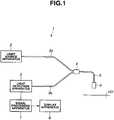
- Fig. 1is a diagram showing a configuration of principal part of an imaging system according to the first embodiment of the present invention.
- Fig. 2is a diagram showing an exemplary configuration of a probe attached to the imaging system shown in Fig. 1 .
- Fig. 3is a diagram showing an example of a spiral pattern used in forming an optical Fourier mask.
- Fig. 4is a diagram showing an exemplary configuration of a probe attached to the imaging system shown in Fig. 1 , where the exemplary configuration is different from the one shown in Fig. 2 .
- an imaging system 1includes a light source apparatus 2, illuminating-light guiding member 2a, light detection apparatus 3, reflected-light guiding member 3a, optical directional coupler 4, transmit/receive optical fiber 5, probe 6, signal processing apparatus 7, and display apparatus 8, where the light source apparatus 2 serves as a light source unit.
- the light source apparatus 2emits illuminating light to illuminate an object 101 such as living tissue. Also, the light source apparatus 2 is configured to be able to emit pulsed light or continuous light as the illuminating light. Alternatively, the light source apparatus 2 may be configured to emit light in a predetermined band as the illuminating light. Also, the light source apparatus 2 may be configured to be able to switch the type of illuminating light according to imaging mode, emitting white light when the object 101 is observed using full color images and emitting band-limited light when the object 101 is observed using spectral images.
- the optical directional coupler 4is configured to emit the light received from the illuminating-light guiding member 2a to the transmit/receive optical fiber 5 and emit the light received from the transmit/receive optical fiber 5 to the reflected-light guiding member 3a. Consequently, the illuminating light from the light source apparatus 2 is transmitted by the illuminating-light guiding member 2a, optical directional coupler 4, and transmit/receive optical fiber 5, and is then incident on the probe 6. That is, an illuminating-light transmitting unit of the imaging system 1 is made up of the illuminating-light guiding member 2a, optical directional coupler 4, and transmit/receive optical fiber 5.
- the probe 6includes an end portion of the transmit/receive optical fiber 5, a collimating lens 6a, and an optical Fourier mask 6b, which are arranged in this order from a proximal side to a distal side. That is, the optical Fourier mask 6b of the imaging system 1 is installed between the end portion of the transmit/receive optical fiber 5 and the object 101.
- the collimating lens 6aemits parallel light to the optical Fourier mask 6b by receiving light from the end portion of the transmit/receive optical fiber 5 as well as collects and focuses light from the optical Fourier mask 6b onto the end portion of the transmit/receive optical fiber 5.
- the optical Fourier mask 6bwhich functions as a timing adjustment unit, causes the illuminating light passing through the collimating lens 6a to be emitted to the object 101 as a light with a spiral pattern, for example, as shown in Fig. 3 . It is assumed that all points on the spiral pattern are set at different distances from a center of the spiral pattern.
- the illuminating light transmitted to the probe 6is emitted to the object 101 through the collimating lens 6a and optical Fourier mask 6b. Then, after being reflected by a surface of the object 101, the illuminating light is incident on the probe 6 as a reflected light. After passing through the optical Fourier mask 6b, collimating lens 6a, transmit/receive optical fiber 5, optical directional coupler 4, and reflected-light guiding member 3a in sequence, the reflected light is incident on the light detection apparatus 3. Incidentally, it is assumed that a reflected-light incidence unit of the imaging system 1 is embodied by (the end portion of) the transmit/receive optical fiber 5 placed in the probe 6.
- the light detection apparatus 3serving as a light detection unit receives light emitted from the reflected-light guiding member 3a, temporally breaks down the light, converts the light into an electrical signal, and outputs the electrical signal in sequence to the signal processing apparatus 7.
- the light detection apparatus 3includes, for example, a point detector and a sensor such as a CCD or CMOS.
- the signal processing apparatus 7serving as a signal processing unit converts the electrical signal outputted in sequence by the light detection apparatus 3 into pixel information about an optical image of the object 101 and accumulates the pixel information. Upon detecting that one screen of the pixel information has been accumulated, the signal processing apparatus 7 outputs the one screen of pixel information as an image signal to the display apparatus 8. Consequently, the display apparatus 8 displays images of the object 101 for observation according to the image signal.
- a userplaces a distal end face of the probe 6 approximately in parallel to the surface of the object 101 by moving the probe 6. Consequently, the illuminating light emitted from the probe 6 is emitted approximately vertically to the surface of the object 101.
- the userturns on power to various parts of the imaging system 1 to emit pulsed or continuous illuminating light from the light source apparatus 2.
- the illuminating light emitted from the light source apparatus 2passes through the illuminating-light guiding member 2a, optical directional coupler 4, transmit/receive optical fiber 5, and collimating lens 6a, and then the optical Fourier mask 6b.
- the time required to reach the surface of the object 101(and thus, timing of arrival at the surface of the object 101) varies among rays contained in the illuminating light which has passed through the optical Fourier mask 6b. That is, the rays contained in the illuminating light emitted from a distal end portion of the probe 6 are reflected from the surface of the object 101 with different reflection timings.
- the light detection apparatus 3receives and temporally breaks down the light incident upon the light detection apparatus 3, converts the light into an electrical signal, and outputs the electrical signal in sequence to the signal processing apparatus 7.
- the signal processing apparatus 7converts the electrical signal outputted in sequence by the light detection apparatus 3 into pixel information about an optical image of the object 101 and accumulates the pixel information. There is no temporal overlap among multiple pieces of pixel information generated and accumulated by the signal processing apparatus 7. Thus, the signal processing apparatus 7 simultaneously generates and accumulates the pixel information by uniquely identifying the pixel information at any location on a plane (surface) of the object 101.
- the signal processing apparatus 7Upon detecting that one screen of pixel information has been accumulated, the signal processing apparatus 7 outputs the one screen of pixel information as an image signal to the display apparatus 8. Consequently, the display apparatus 8 displays an image of the object 101 in which planar orientation can be identified sufficiently.
- the imaging system 1ensures that the rays contained in the illuminating light emitted from the distal end portion of the probe 6 will be reflected from the surface of the object 101 with different reflection timings. Consequently, the imaging system 1 according to the present embodiment can acquire information about the surface of an object accurately when scanning the surface of the object with light.
- the imaging system 1is not limited to a configuration in which the illuminating-light guiding member 2a and reflected-light guiding member 3a are installed separately, and may have a configuration in which the illuminating-light guiding member 2a and reflected-light guiding member 3a are formed integrally.
- the imaging system 1is not limited to a configuration in which the collimating lens 6a and optical Fourier mask 6b are provided as separate optical members, and, for example, may have an optical member which combines the functions of the collimating lens 6a and optical Fourier mask 6b.
- the imaging system 1may be configured to transmit and receive light, for example, by vibrating the end portion of the transmit/receive optical fiber 5 placed in the probe 6.
- the imaging system 1may have a probe 6A shown in Fig. 4 instead of the probe 6 shown in Fig. 2
- the probe 6Aincludes an end portion of the transmit/receive optical fiber 5, a collimating lens 6a, an optical Fourier mask 6b, and an objective optical system 6c, which are arranged in this order from the proximal side to the distal side.
- the objective optical system 6cis configured to be able to extend an emission range of the illuminating light passed through the optical Fourier mask 6b and allows the light reflected from the surface of the object 101 to pass by maintaining its course.
- the use of the probe 6A with this configurationmakes it possible to acquire information from a wider area on the surface of the object 101.
- a shuttermay be installed in front of a light-receiving unit of the light detection apparatus 3 and the timing of emission of the illuminating light from the light source apparatus 2 may be synchronized with the timing of opening and closing of the shutter.
- Figs. 5 and 6concern a second embodiment of the present invention.
- Fig. 5is a diagram showing a configuration of principal part of an imaging system according to the second embodiment of the present invention.
- Fig. 6is a diagram showing an exemplary configuration of a probe attached to the imaging system shown in Fig. 5 .
- An imaging system according to the present embodimenthas a configuration similar to the configuration of the imaging system 1 according to the first embodiment. Thus, parts different from the imaging system 1 according to the first embodiment will mainly be described in the second embodiment.
- an imaging system 1Aincludes a light source apparatus 2, illuminating-light guiding member 2a, light detection apparatus 3, reflected-light guiding member 3a, probe 6B, signal processing apparatus 7, and display apparatus 8.
- the probe 6Bincludes an end portion of the illuminating-light guiding member 2a, a collimating lens 61, an optical Fourier mask 6b, and a polarizer 62, which are arranged in order from the proximal side to the distal side.
- the illuminating light emitted from the light source apparatus 2is emitted to the surface of the object 101 after passing through the above-described components in order. That is, an illuminating-light transmitting unit of the imaging system 1A is made up of an illuminating-light guiding member 2a.
- the optical Fourier mask 6b of the imaging system 1Ais installed between an end portion of the illuminating-light guiding member 2a and the object 101.
- the polarizer 62 of the imaging system 1Ais installed between the optical Fourier mask 6b and object 101.
- the probe 6Bincludes an analyzer 63, a collimating lens 64, and an end portion of the reflected-light guiding member 3a, which are arranged in this order from the proximal side to the distal side.
- the light reflected from the surface of the object 101is finally transmitted to the light detection apparatus 3 after passing through the above-described components in order.
- a reflected-light incidence unit of the imaging system 1Ais embodied by (the end portion of) the reflected-light guiding member 3a placed in the probe 6B.
- the analyzer 63 of the imaging system 1Ais installed between the object 101 and the end portion of reflected-light guiding member 3a.
- the collimating lens 61emits parallel light to the optical Fourier mask 6b by receiving light from the end portion of the illuminating-light guiding member 2a.
- the polarizer 62emits the illuminating light passed through the optical Fourier mask 6b to the surface of the object 101 by aligning the illuminating light along a first polarizing direction.
- rays contained in the illuminating light emitted from the light source apparatus 2have a spiral pattern and are emitted to the surface of the object 101 by being uniformly polarized along a first polarizing direction.
- the analyzer 63emits the light reflected by the object 101 to the collimating lens 64 by aligning the light along a second polarizing direction orthogonal to the first polarizing direction. Consequently, the analyzer 63 removes a component reflected by a depth (inner part) of the object 101 from the light reflected by the object 101 and thereby extracts only a component reflected by the surface of the object 101.
- the collimating lens 64collects and focuses the light passing through the analyzer 63 on the end portion of the reflected-light guiding member 3a.
- This configurationcauses the rays contained in the light reflected by the object 101 to have different reflecting timings: the rays are incident upon the end portion of the reflected-light guiding member 3a, being uniformly polarized along the second polarizing direction, and eventually transmitted to the light detection apparatus 3.
- the light detection apparatus 3receives and temporally breaks down the light incident upon the light detection apparatus 3, converts the light into an electrical signal, and outputs the electrical signal in sequence to the signal processing apparatus 7.
- the signal processing apparatus 7converts the electrical signal outputted in sequence by the light detection apparatus 3 into pixel information about an optical image of the object 101 and accumulates the pixel information. There is no temporal overlap among multiple pieces of pixel information generated and accumulated by the signal processing apparatus 7. Thus, the signal processing apparatus 7 simultaneously accumulates and generates the pixel information by uniquely identifying the pixel information at any location on a plane of the object 101.
- the signal processing apparatus 7Upon detecting that one screen of pixel information has been accumulated, the signal processing apparatus 7 outputs the one screen of pixel information as an image signal to the display apparatus 8. Consequently, the display apparatus 8 displays an image of the object 101, where the image allows planar orientation to be identified sufficiently, and the object 101 to be observed in detail.
- the imaging system 1Acan acquire information about the surface of an object more accurately when scanning the surface of the object with light.
- the second polarizing direction of the analyzer 63does not necessarily need to be orthogonal to the first polarizing direction of the polarizer 62 as long as the second polarizing direction is different from the first polarizing direction.
Landscapes
- Life Sciences & Earth Sciences (AREA)
- Health & Medical Sciences (AREA)
- Medical Informatics (AREA)
- Molecular Biology (AREA)
- Pathology (AREA)
- Engineering & Computer Science (AREA)
- Biomedical Technology (AREA)
- Heart & Thoracic Surgery (AREA)
- Physics & Mathematics (AREA)
- Biophysics (AREA)
- Surgery (AREA)
- Animal Behavior & Ethology (AREA)
- General Health & Medical Sciences (AREA)
- Public Health (AREA)
- Veterinary Medicine (AREA)
- Investigating Or Analysing Materials By Optical Means (AREA)
- Endoscopes (AREA)
- Instruments For Viewing The Inside Of Hollow Bodies (AREA)
Description
- The present invention relates to an imaging system and, in particular, to an imaging system which allows a condition on a surface of an object to be observed by scanning the surface of the object with light.
- A technique for acquiring information about a surface of an object by scanning the surface of the object with light has been proposed in recent years. An example of such a technique is described in Japanese Patent Application Laid-Open Publication No.
2005-87468 - The technique disclosed in Japanese Patent Application Laid-Open Publication No.
2005-87468 - However, with an imaging system disclosed in Japanese Patent Application Laid-Open Publication No.
2005-87468 - Thus, the imaging system described in Japanese Patent Application Laid-Open Publication No.
2005-87468 2005-87468 WO 2007/084915 A2 discloses a fiber-optic scanning endoscope for non-linear optical imaging and spectroscopy. The endoscope uses a tubular piezoelectric actuator for activating a cantilevered optical fiber from which pulse light produced by a laser source exits and is directed to a target region through a micro-lense. The activator is activated by two modulated signals that achieve two-dimensional beam scanning in a desired scan pattern. A double-clad optical fiber is employed for delivery of the excitation pulsed light and collection of emitted light received from the target region. The pulse light travels through a core of the double-clad optical fiber, and the emitted light from the target region is directed into the core and inner cladding of the optical fiber and conveyed to a proximal end, for detection and processing. The emitted light can include multiphoton fluorescence, second harmonic generation light and spectroscopic information for imaging.- The present invention has been made in view of the above circumstances and has an object to provide an imaging system which can acquire information about a surface of an object more accurately when scanning the surface of the object with light.
- The present invention provides an imaging system as set out in
independent claim 1. Fig. 1 is a diagram showing a configuration of principal part of an imaging system according to a first embodiment of the present invention;Fig. 2 is a diagram showing an exemplary configuration of a probe attached to the imaging system shown inFig. 1 ;Fig. 3 is a diagram showing an example of a spiral pattern used in forming an optical Fourier mask;Fig. 4 is a diagram showing an exemplary configuration of a probe attached to the imaging system shown inFig. 1 , where the exemplary configuration is different from the one shown inFig. 2 ;Fig. 5 is a diagram showing a configuration of principal part of an imaging system according to a second embodiment of the present invention; andFig. 6 is a diagram showing an exemplary configuration of a probe attached to the imaging system shown inFig. 5 .- Embodiments of the present invention will be described below with reference to the drawings.
Figs. 1 to 4 concern a first embodiment of the present invention.Fig. 1 is a diagram showing a configuration of principal part of an imaging system according to the first embodiment of the present invention.Fig. 2 is a diagram showing an exemplary configuration of a probe attached to the imaging system shown inFig. 1 .Fig. 3 is a diagram showing an example of a spiral pattern used in forming an optical Fourier mask.Fig. 4 is a diagram showing an exemplary configuration of a probe attached to the imaging system shown inFig. 1 , where the exemplary configuration is different from the one shown inFig. 2 .- As shown in
Fig. 1 , animaging system 1 includes alight source apparatus 2, illuminating-light guidingmember 2a,light detection apparatus 3, reflected-light guidingmember 3a, optical directional coupler 4, transmit/receiveoptical fiber 5,probe 6,signal processing apparatus 7, anddisplay apparatus 8, where thelight source apparatus 2 serves as a light source unit. - The
light source apparatus 2 emits illuminating light to illuminate anobject 101 such as living tissue. Also, thelight source apparatus 2 is configured to be able to emit pulsed light or continuous light as the illuminating light. Alternatively, thelight source apparatus 2 may be configured to emit light in a predetermined band as the illuminating light. Also, thelight source apparatus 2 may be configured to be able to switch the type of illuminating light according to imaging mode, emitting white light when theobject 101 is observed using full color images and emitting band-limited light when theobject 101 is observed using spectral images. - The optical directional coupler 4 is configured to emit the light received from the illuminating-light guiding
member 2a to the transmit/receiveoptical fiber 5 and emit the light received from the transmit/receiveoptical fiber 5 to the reflected-light guidingmember 3a. Consequently, the illuminating light from thelight source apparatus 2 is transmitted by the illuminating-light guidingmember 2a, optical directional coupler 4, and transmit/receiveoptical fiber 5, and is then incident on theprobe 6. That is, an illuminating-light transmitting unit of theimaging system 1 is made up of the illuminating-light guidingmember 2a, optical directional coupler 4, and transmit/receiveoptical fiber 5. - As shown in
Fig. 2 , theprobe 6 includes an end portion of the transmit/receiveoptical fiber 5, acollimating lens 6a, and anoptical Fourier mask 6b, which are arranged in this order from a proximal side to a distal side. That is, the optical Fouriermask 6b of theimaging system 1 is installed between the end portion of the transmit/receiveoptical fiber 5 and theobject 101. - The
collimating lens 6a emits parallel light to the optical Fouriermask 6b by receiving light from the end portion of the transmit/receiveoptical fiber 5 as well as collects and focuses light from theoptical Fourier mask 6b onto the end portion of the transmit/receiveoptical fiber 5. - The optical Fourier
mask 6b, which functions as a timing adjustment unit, causes the illuminating light passing through thecollimating lens 6a to be emitted to theobject 101 as a light with a spiral pattern, for example, as shown inFig. 3 . It is assumed that all points on the spiral pattern are set at different distances from a center of the spiral pattern. - Consequently, the illuminating light transmitted to the
probe 6 is emitted to theobject 101 through thecollimating lens 6a and optical Fouriermask 6b. Then, after being reflected by a surface of theobject 101, the illuminating light is incident on theprobe 6 as a reflected light. After passing through the optical Fouriermask 6b,collimating lens 6a, transmit/receiveoptical fiber 5, optical directional coupler 4, and reflected-light guidingmember 3a in sequence, the reflected light is incident on thelight detection apparatus 3. Incidentally, it is assumed that a reflected-light incidence unit of theimaging system 1 is embodied by (the end portion of) the transmit/receiveoptical fiber 5 placed in theprobe 6. - The
light detection apparatus 3 serving as a light detection unit receives light emitted from the reflected-light guidingmember 3a, temporally breaks down the light, converts the light into an electrical signal, and outputs the electrical signal in sequence to thesignal processing apparatus 7. To implement this function, thelight detection apparatus 3 includes, for example, a point detector and a sensor such as a CCD or CMOS. - The
signal processing apparatus 7 serving as a signal processing unit converts the electrical signal outputted in sequence by thelight detection apparatus 3 into pixel information about an optical image of theobject 101 and accumulates the pixel information. Upon detecting that one screen of the pixel information has been accumulated, thesignal processing apparatus 7 outputs the one screen of pixel information as an image signal to thedisplay apparatus 8. Consequently, thedisplay apparatus 8 displays images of theobject 101 for observation according to the image signal. - Next, operation of the
imaging system 1 will be described. - First, a user places a distal end face of the
probe 6 approximately in parallel to the surface of theobject 101 by moving theprobe 6. Consequently, the illuminating light emitted from theprobe 6 is emitted approximately vertically to the surface of theobject 101. - The user turns on power to various parts of the
imaging system 1 to emit pulsed or continuous illuminating light from thelight source apparatus 2. - The illuminating light emitted from the
light source apparatus 2 passes through the illuminating-light guidingmember 2a, optical directional coupler 4, transmit/receiveoptical fiber 5, and collimatinglens 6a, and then the optical Fouriermask 6b. - The time required to reach the surface of the object 101 (and thus, timing of arrival at the surface of the object 101) varies among rays contained in the illuminating light which has passed through the
optical Fourier mask 6b. That is, the rays contained in the illuminating light emitted from a distal end portion of theprobe 6 are reflected from the surface of theobject 101 with different reflection timings. - Rays contained in the light reflected from the surface of the
object 101 are incident upon theprobe 6 with different timings. Then, after passing through the optical directional coupler 4 and reflected-light guiding member 3a in sequence, the rays are incident upon thelight detection apparatus 3. - The
light detection apparatus 3 receives and temporally breaks down the light incident upon thelight detection apparatus 3, converts the light into an electrical signal, and outputs the electrical signal in sequence to thesignal processing apparatus 7. - The
signal processing apparatus 7 converts the electrical signal outputted in sequence by thelight detection apparatus 3 into pixel information about an optical image of theobject 101 and accumulates the pixel information. There is no temporal overlap among multiple pieces of pixel information generated and accumulated by thesignal processing apparatus 7. Thus, thesignal processing apparatus 7 simultaneously generates and accumulates the pixel information by uniquely identifying the pixel information at any location on a plane (surface) of theobject 101. - Upon detecting that one screen of pixel information has been accumulated, the
signal processing apparatus 7 outputs the one screen of pixel information as an image signal to thedisplay apparatus 8. Consequently, thedisplay apparatus 8 displays an image of theobject 101 in which planar orientation can be identified sufficiently. - As described above, by using the
optical Fourier mask 6b which generates a light with a spiral pattern, theimaging system 1 according to the present embodiment ensures that the rays contained in the illuminating light emitted from the distal end portion of theprobe 6 will be reflected from the surface of theobject 101 with different reflection timings. Consequently, theimaging system 1 according to the present embodiment can acquire information about the surface of an object accurately when scanning the surface of the object with light. - Incidentally, the
imaging system 1 according to the present embodiment is not limited to a configuration in which the illuminating-light guiding member 2a and reflected-light guiding member 3a are installed separately, and may have a configuration in which the illuminating-light guiding member 2a and reflected-light guiding member 3a are formed integrally. - Also, the
imaging system 1 according to the present embodiment is not limited to a configuration in which thecollimating lens 6a andoptical Fourier mask 6b are provided as separate optical members, and, for example, may have an optical member which combines the functions of thecollimating lens 6a andoptical Fourier mask 6b. - Furthermore, the
imaging system 1 according to the present embodiment may be configured to transmit and receive light, for example, by vibrating the end portion of the transmit/receiveoptical fiber 5 placed in theprobe 6. - Besides, the
imaging system 1 according to the present embodiment may have aprobe 6A shown inFig. 4 instead of theprobe 6 shown inFig. 2 - As shown in
Fig. 4 , theprobe 6A includes an end portion of the transmit/receiveoptical fiber 5, acollimating lens 6a, anoptical Fourier mask 6b, and an objectiveoptical system 6c, which are arranged in this order from the proximal side to the distal side. - The objective
optical system 6c is configured to be able to extend an emission range of the illuminating light passed through theoptical Fourier mask 6b and allows the light reflected from the surface of theobject 101 to pass by maintaining its course. - The use of the
probe 6A with this configuration makes it possible to acquire information from a wider area on the surface of theobject 101. - With the
imaging system 1 according to the present embodiment, a shutter may be installed in front of a light-receiving unit of thelight detection apparatus 3 and the timing of emission of the illuminating light from thelight source apparatus 2 may be synchronized with the timing of opening and closing of the shutter. Figs. 5 and6 concern a second embodiment of the present invention.Fig. 5 is a diagram showing a configuration of principal part of an imaging system according to the second embodiment of the present invention.Fig. 6 is a diagram showing an exemplary configuration of a probe attached to the imaging system shown inFig. 5 .- Detailed description of components similar to those of the first embodiment will be omitted below. An imaging system according to the present embodiment has a configuration similar to the configuration of the
imaging system 1 according to the first embodiment. Thus, parts different from theimaging system 1 according to the first embodiment will mainly be described in the second embodiment. - As shown in
Fig. 5 , animaging system 1A includes alight source apparatus 2, illuminating-light guiding member 2a,light detection apparatus 3, reflected-light guiding member 3a,probe 6B,signal processing apparatus 7, anddisplay apparatus 8. - As shown in
Fig. 6 , theprobe 6B includes an end portion of the illuminating-light guiding member 2a, a collimatinglens 61, anoptical Fourier mask 6b, and apolarizer 62, which are arranged in order from the proximal side to the distal side. The illuminating light emitted from thelight source apparatus 2 is emitted to the surface of theobject 101 after passing through the above-described components in order. That is, an illuminating-light transmitting unit of theimaging system 1A is made up of an illuminating-light guiding member 2a. Theoptical Fourier mask 6b of theimaging system 1A is installed between an end portion of the illuminating-light guiding member 2a and theobject 101. Furthermore, thepolarizer 62 of theimaging system 1A is installed between theoptical Fourier mask 6b andobject 101. - Also, as shown in
Fig. 6 , theprobe 6B includes ananalyzer 63, a collimatinglens 64, and an end portion of the reflected-light guiding member 3a, which are arranged in this order from the proximal side to the distal side. The light reflected from the surface of theobject 101 is finally transmitted to thelight detection apparatus 3 after passing through the above-described components in order. Incidentally, a reflected-light incidence unit of theimaging system 1A is embodied by (the end portion of) the reflected-light guiding member 3a placed in theprobe 6B. Also, theanalyzer 63 of theimaging system 1A is installed between theobject 101 and the end portion of reflected-light guiding member 3a. - The collimating
lens 61 emits parallel light to theoptical Fourier mask 6b by receiving light from the end portion of the illuminating-light guiding member 2a. - The
polarizer 62 emits the illuminating light passed through theoptical Fourier mask 6b to the surface of theobject 101 by aligning the illuminating light along a first polarizing direction. - With this configuration, rays contained in the illuminating light emitted from the
light source apparatus 2 have a spiral pattern and are emitted to the surface of theobject 101 by being uniformly polarized along a first polarizing direction. - The
analyzer 63 emits the light reflected by theobject 101 to thecollimating lens 64 by aligning the light along a second polarizing direction orthogonal to the first polarizing direction. Consequently, theanalyzer 63 removes a component reflected by a depth (inner part) of theobject 101 from the light reflected by theobject 101 and thereby extracts only a component reflected by the surface of theobject 101. - The collimating
lens 64 collects and focuses the light passing through theanalyzer 63 on the end portion of the reflected-light guiding member 3a. - This configuration causes the rays contained in the light reflected by the
object 101 to have different reflecting timings: the rays are incident upon the end portion of the reflected-light guiding member 3a, being uniformly polarized along the second polarizing direction, and eventually transmitted to thelight detection apparatus 3. - The
light detection apparatus 3 receives and temporally breaks down the light incident upon thelight detection apparatus 3, converts the light into an electrical signal, and outputs the electrical signal in sequence to thesignal processing apparatus 7. - The
signal processing apparatus 7 converts the electrical signal outputted in sequence by thelight detection apparatus 3 into pixel information about an optical image of theobject 101 and accumulates the pixel information. There is no temporal overlap among multiple pieces of pixel information generated and accumulated by thesignal processing apparatus 7. Thus, thesignal processing apparatus 7 simultaneously accumulates and generates the pixel information by uniquely identifying the pixel information at any location on a plane of theobject 101. - Upon detecting that one screen of pixel information has been accumulated, the
signal processing apparatus 7 outputs the one screen of pixel information as an image signal to thedisplay apparatus 8. Consequently, thedisplay apparatus 8 displays an image of theobject 101, where the image allows planar orientation to be identified sufficiently, and theobject 101 to be observed in detail. - As described above, the
imaging system 1A according to the present embodiment can acquire information about the surface of an object more accurately when scanning the surface of the object with light. - The second polarizing direction of the
analyzer 63 does not necessarily need to be orthogonal to the first polarizing direction of thepolarizer 62 as long as the second polarizing direction is different from the first polarizing direction.
Claims (4)
- An imaging system (1), comprising:a light source unit (2) which emits illuminating light to illuminate an object;an illuminating-light transmitting unit (5) which transmits the illuminating light;a timing adjustment unit (6b), which, being placed between the illuminating-light transmitting unit (5) and the object (101), consists of an optical Fourier mask (6b) for generating light with a light spiral pattern so as to vary timing with which rays contained in the illuminating light which has passed through the illuminating-light transmitting unit (5) reach a surface of the object (101) and emits the light with the predetermined pattern generated by the optical Fourier mask (6b);a reflected-light incidence unit upon which reflected light coming from the surface of the object is incident;a light detection unit (3) which temporally breaks down the reflected light incident upon the reflected-light incidence unit, converts the reflected light into an electrical signal, and outputs the electrical signal in sequence; anda signal processing unit (7) which converts the electrical signal outputted in sequence by the light detection unit (3) into pixel information about an optical image on the surface of the object (101).
- The imaging system (1) according to claim 1, wherein the light source unit (2) emits pulsed light as the illuminating light.
- The imaging system (1) according to claim 1, wherein the light source unit (2) emits continuous light as the illuminating light.
- The imaging system (1) according to claim 1, further comprising:a polarizer (62) which, being installed between the illuminating-light emitting unit and the object, aligns the light with the predetermined pattern which has passed through the illuminating-light emitting unit along a first polarizing direction; andan analyzer (63) which, being installed between the object and the reflected-light incidence unit, aligns the light reflected by the surface of the object along a second polarizing direction orthogonal to the first polarizing direction.
Applications Claiming Priority (1)
| Application Number | Priority Date | Filing Date | Title |
|---|---|---|---|
| JP2008227141AJP5242304B2 (en) | 2008-09-04 | 2008-09-04 | Observation system |
Publications (2)
| Publication Number | Publication Date |
|---|---|
| EP2160974A1 EP2160974A1 (en) | 2010-03-10 |
| EP2160974B1true EP2160974B1 (en) | 2016-06-22 |
Family
ID=41509015
Family Applications (1)
| Application Number | Title | Priority Date | Filing Date |
|---|---|---|---|
| EP09008554.9AActiveEP2160974B1 (en) | 2008-09-04 | 2009-06-30 | Imaging system |
Country Status (3)
| Country | Link |
|---|---|
| US (1) | US8278615B2 (en) |
| EP (1) | EP2160974B1 (en) |
| JP (1) | JP5242304B2 (en) |
Families Citing this family (3)
| Publication number | Priority date | Publication date | Assignee | Title |
|---|---|---|---|---|
| US8702321B2 (en)* | 2009-12-03 | 2014-04-22 | Eric T. Marple | Filtered fiber optic probe |
| CN102410850A (en)* | 2010-09-21 | 2012-04-11 | 王建伟 | Reflective optical fiber sensor device |
| JP6535020B2 (en) | 2014-03-02 | 2019-06-26 | ブイ.ティー.エム.(バーチャル テープ メジャー)テクノロジーズ リミテッド | System for measuring 3D distance and dimensions of visible objects in endoscopic images |
Family Cites Families (8)
| Publication number | Priority date | Publication date | Assignee | Title |
|---|---|---|---|---|
| US5001556A (en)* | 1987-09-30 | 1991-03-19 | Olympus Optical Co., Ltd. | Endoscope apparatus for processing a picture image of an object based on a selected wavelength range |
| JPH07243820A (en)* | 1994-03-04 | 1995-09-19 | Toshiba Corp | Surface shape measuring device |
| US5719399A (en)* | 1995-12-18 | 1998-02-17 | The Research Foundation Of City College Of New York | Imaging and characterization of tissue based upon the preservation of polarized light transmitted therethrough |
| JP4239166B2 (en)* | 2002-12-27 | 2009-03-18 | 関西ティー・エル・オー株式会社 | Multilayer observation type optical microscope and multilayer observation unit |
| JP2005087468A (en)* | 2003-09-17 | 2005-04-07 | Shoji Kawahito | Image pickup device provided with distance image measurement function and endoscopic apparatus |
| JP4327738B2 (en) | 2005-01-18 | 2009-09-09 | 株式会社東芝 | Biological light measurement device and biological light measurement method |
| WO2007079805A1 (en)* | 2006-01-08 | 2007-07-19 | Hermann Tropf | Creation of a distance image |
| US20070213618A1 (en)* | 2006-01-17 | 2007-09-13 | University Of Washington | Scanning fiber-optic nonlinear optical imaging and spectroscopy endoscope |
- 2008
- 2008-09-04JPJP2008227141Apatent/JP5242304B2/enactiveActive
- 2009
- 2009-06-30EPEP09008554.9Apatent/EP2160974B1/enactiveActive
- 2009-08-31USUS12/550,828patent/US8278615B2/enactiveActive
Also Published As
| Publication number | Publication date |
|---|---|
| EP2160974A1 (en) | 2010-03-10 |
| JP5242304B2 (en) | 2013-07-24 |
| US8278615B2 (en) | 2012-10-02 |
| JP2010057740A (en) | 2010-03-18 |
| US20100051789A1 (en) | 2010-03-04 |
Similar Documents
| Publication | Publication Date | Title |
|---|---|---|
| JP5133595B2 (en) | Illumination light detection optical system, and optical apparatus and endoscope apparatus including the same | |
| EP2263517B1 (en) | Endoscope observation device | |
| US8123679B2 (en) | Endoscope apparatus | |
| JP5025877B2 (en) | Medical imaging, diagnosis and treatment using a scanning single fiber optic system | |
| US11723526B2 (en) | Device and method for observing an object, taking into consideration the distance between the device and the object | |
| US8721525B2 (en) | Endoscope system with a modulated radiation source | |
| JP4471163B2 (en) | Optical tomographic image acquisition device | |
| US8423110B2 (en) | Imaging device and related methods | |
| US6527708B1 (en) | Endoscope system | |
| US20070184402A1 (en) | Caries detection using real-time imaging and multiple excitation frequencies | |
| JP2008237236A (en) | Endoscope and living body observation system | |
| JP2017176811A5 (en) | ||
| JP2011030735A (en) | Endoscope shape detector and endoscope system | |
| US20100290100A1 (en) | Confocal optical system | |
| EP2160974B1 (en) | Imaging system | |
| JP6748933B2 (en) | Terahertz irradiation position visualization device | |
| JP2006026015A (en) | Optical tomographic image acquisition system | |
| CN107430270A (en) | Scanning trajectory measurement method of optical scanning device, scanning trajectory measurement device, and image calibration method | |
| JP2011050667A (en) | Optical scan type endoscope | |
| US20070293766A1 (en) | Transmission Based Imaging for Spectroscopic Analysis | |
| US7049596B2 (en) | Method and apparatus for distinguishing materials | |
| JP6599722B2 (en) | Inspection device | |
| JP4647449B2 (en) | Sample analyzer | |
| JP2013036991A (en) | Optical observation device | |
| JPH0541901A (en) | Endoscope for three-dimensional measurement |
Legal Events
| Date | Code | Title | Description |
|---|---|---|---|
| PUAI | Public reference made under article 153(3) epc to a published international application that has entered the european phase | Free format text:ORIGINAL CODE: 0009012 | |
| AK | Designated contracting states | Kind code of ref document:A1 Designated state(s):AT BE BG CH CY CZ DE DK EE ES FI FR GB GR HR HU IE IS IT LI LT LU LV MC MK MT NL NO PL PT RO SE SI SK TR | |
| AX | Request for extension of the european patent | Extension state:AL BA RS | |
| 17P | Request for examination filed | Effective date:20100504 | |
| 17Q | First examination report despatched | Effective date:20100609 | |
| RAP1 | Party data changed (applicant data changed or rights of an application transferred) | Owner name:OLYMPUS CORPORATION | |
| GRAP | Despatch of communication of intention to grant a patent | Free format text:ORIGINAL CODE: EPIDOSNIGR1 | |
| INTG | Intention to grant announced | Effective date:20151222 | |
| GRAJ | Information related to disapproval of communication of intention to grant by the applicant or resumption of examination proceedings by the epo deleted | Free format text:ORIGINAL CODE: EPIDOSDIGR1 | |
| GRAL | Information related to payment of fee for publishing/printing deleted | Free format text:ORIGINAL CODE: EPIDOSDIGR3 | |
| GRAR | Information related to intention to grant a patent recorded | Free format text:ORIGINAL CODE: EPIDOSNIGR71 | |
| GRAS | Grant fee paid | Free format text:ORIGINAL CODE: EPIDOSNIGR3 | |
| GRAA | (expected) grant | Free format text:ORIGINAL CODE: 0009210 | |
| INTG | Intention to grant announced | Effective date:20160512 | |
| AK | Designated contracting states | Kind code of ref document:B1 Designated state(s):AT BE BG CH CY CZ DE DK EE ES FI FR GB GR HR HU IE IS IT LI LT LU LV MC MK MT NL NO PL PT RO SE SI SK TR | |
| REG | Reference to a national code | Ref country code:GB Ref legal event code:FG4D | |
| REG | Reference to a national code | Ref country code:CH Ref legal event code:EP | |
| REG | Reference to a national code | Ref country code:IE Ref legal event code:FG4D | |
| REG | Reference to a national code | Ref country code:AT Ref legal event code:REF Ref document number:807165 Country of ref document:AT Kind code of ref document:T Effective date:20160715 | |
| REG | Reference to a national code | Ref country code:DE Ref legal event code:R096 Ref document number:602009039298 Country of ref document:DE | |
| RAP2 | Party data changed (patent owner data changed or rights of a patent transferred) | Owner name:OLYMPUS CORPORATION | |
| RAP2 | Party data changed (patent owner data changed or rights of a patent transferred) | Owner name:OLYMPUS CORPORATION | |
| REG | Reference to a national code | Ref country code:LT Ref legal event code:MG4D | |
| REG | Reference to a national code | Ref country code:NL Ref legal event code:MP Effective date:20160622 | |
| PG25 | Lapsed in a contracting state [announced via postgrant information from national office to epo] | Ref country code:FI Free format text:LAPSE BECAUSE OF FAILURE TO SUBMIT A TRANSLATION OF THE DESCRIPTION OR TO PAY THE FEE WITHIN THE PRESCRIBED TIME-LIMIT Effective date:20160622 Ref country code:NO Free format text:LAPSE BECAUSE OF FAILURE TO SUBMIT A TRANSLATION OF THE DESCRIPTION OR TO PAY THE FEE WITHIN THE PRESCRIBED TIME-LIMIT Effective date:20160922 Ref country code:LT Free format text:LAPSE BECAUSE OF FAILURE TO SUBMIT A TRANSLATION OF THE DESCRIPTION OR TO PAY THE FEE WITHIN THE PRESCRIBED TIME-LIMIT Effective date:20160622 | |
| REG | Reference to a national code | Ref country code:AT Ref legal event code:MK05 Ref document number:807165 Country of ref document:AT Kind code of ref document:T Effective date:20160622 | |
| RIN2 | Information on inventor provided after grant (corrected) | Inventor name:GONO, KAZUHIRO Inventor name:IGARASHI, MAKOTO | |
| PG25 | Lapsed in a contracting state [announced via postgrant information from national office to epo] | Ref country code:GR Free format text:LAPSE BECAUSE OF FAILURE TO SUBMIT A TRANSLATION OF THE DESCRIPTION OR TO PAY THE FEE WITHIN THE PRESCRIBED TIME-LIMIT Effective date:20160923 Ref country code:LV Free format text:LAPSE BECAUSE OF FAILURE TO SUBMIT A TRANSLATION OF THE DESCRIPTION OR TO PAY THE FEE WITHIN THE PRESCRIBED TIME-LIMIT Effective date:20160622 Ref country code:NL Free format text:LAPSE BECAUSE OF FAILURE TO SUBMIT A TRANSLATION OF THE DESCRIPTION OR TO PAY THE FEE WITHIN THE PRESCRIBED TIME-LIMIT Effective date:20160622 Ref country code:SE Free format text:LAPSE BECAUSE OF FAILURE TO SUBMIT A TRANSLATION OF THE DESCRIPTION OR TO PAY THE FEE WITHIN THE PRESCRIBED TIME-LIMIT Effective date:20160622 Ref country code:HR Free format text:LAPSE BECAUSE OF FAILURE TO SUBMIT A TRANSLATION OF THE DESCRIPTION OR TO PAY THE FEE WITHIN THE PRESCRIBED TIME-LIMIT Effective date:20160622 | |
| PG25 | Lapsed in a contracting state [announced via postgrant information from national office to epo] | Ref country code:BE Free format text:LAPSE BECAUSE OF NON-PAYMENT OF DUE FEES Effective date:20160630 | |
| PG25 | Lapsed in a contracting state [announced via postgrant information from national office to epo] | Ref country code:SK Free format text:LAPSE BECAUSE OF FAILURE TO SUBMIT A TRANSLATION OF THE DESCRIPTION OR TO PAY THE FEE WITHIN THE PRESCRIBED TIME-LIMIT Effective date:20160622 Ref country code:IS Free format text:LAPSE BECAUSE OF FAILURE TO SUBMIT A TRANSLATION OF THE DESCRIPTION OR TO PAY THE FEE WITHIN THE PRESCRIBED TIME-LIMIT Effective date:20161022 Ref country code:RO Free format text:LAPSE BECAUSE OF FAILURE TO SUBMIT A TRANSLATION OF THE DESCRIPTION OR TO PAY THE FEE WITHIN THE PRESCRIBED TIME-LIMIT Effective date:20160622 Ref country code:IT Free format text:LAPSE BECAUSE OF FAILURE TO SUBMIT A TRANSLATION OF THE DESCRIPTION OR TO PAY THE FEE WITHIN THE PRESCRIBED TIME-LIMIT Effective date:20160622 Ref country code:EE Free format text:LAPSE BECAUSE OF FAILURE TO SUBMIT A TRANSLATION OF THE DESCRIPTION OR TO PAY THE FEE WITHIN THE PRESCRIBED TIME-LIMIT Effective date:20160622 Ref country code:CZ Free format text:LAPSE BECAUSE OF FAILURE TO SUBMIT A TRANSLATION OF THE DESCRIPTION OR TO PAY THE FEE WITHIN THE PRESCRIBED TIME-LIMIT Effective date:20160622 | |
| REG | Reference to a national code | Ref country code:CH Ref legal event code:PL | |
| PG25 | Lapsed in a contracting state [announced via postgrant information from national office to epo] | Ref country code:PL Free format text:LAPSE BECAUSE OF FAILURE TO SUBMIT A TRANSLATION OF THE DESCRIPTION OR TO PAY THE FEE WITHIN THE PRESCRIBED TIME-LIMIT Effective date:20160622 Ref country code:AT Free format text:LAPSE BECAUSE OF FAILURE TO SUBMIT A TRANSLATION OF THE DESCRIPTION OR TO PAY THE FEE WITHIN THE PRESCRIBED TIME-LIMIT Effective date:20160622 Ref country code:BE Free format text:LAPSE BECAUSE OF FAILURE TO SUBMIT A TRANSLATION OF THE DESCRIPTION OR TO PAY THE FEE WITHIN THE PRESCRIBED TIME-LIMIT Effective date:20160622 Ref country code:ES Free format text:LAPSE BECAUSE OF FAILURE TO SUBMIT A TRANSLATION OF THE DESCRIPTION OR TO PAY THE FEE WITHIN THE PRESCRIBED TIME-LIMIT Effective date:20160622 Ref country code:PT Free format text:LAPSE BECAUSE OF FAILURE TO SUBMIT A TRANSLATION OF THE DESCRIPTION OR TO PAY THE FEE WITHIN THE PRESCRIBED TIME-LIMIT Effective date:20161024 | |
| REG | Reference to a national code | Ref country code:IE Ref legal event code:MM4A | |
| REG | Reference to a national code | Ref country code:DE Ref legal event code:R097 Ref document number:602009039298 Country of ref document:DE | |
| PG25 | Lapsed in a contracting state [announced via postgrant information from national office to epo] | Ref country code:MC Free format text:LAPSE BECAUSE OF FAILURE TO SUBMIT A TRANSLATION OF THE DESCRIPTION OR TO PAY THE FEE WITHIN THE PRESCRIBED TIME-LIMIT Effective date:20160622 | |
| PG25 | Lapsed in a contracting state [announced via postgrant information from national office to epo] | Ref country code:CH Free format text:LAPSE BECAUSE OF NON-PAYMENT OF DUE FEES Effective date:20160630 Ref country code:LI Free format text:LAPSE BECAUSE OF NON-PAYMENT OF DUE FEES Effective date:20160630 | |
| PLBE | No opposition filed within time limit | Free format text:ORIGINAL CODE: 0009261 | |
| STAA | Information on the status of an ep patent application or granted ep patent | Free format text:STATUS: NO OPPOSITION FILED WITHIN TIME LIMIT | |
| REG | Reference to a national code | Ref country code:FR Ref legal event code:ST Effective date:20170331 | |
| GBPC | Gb: european patent ceased through non-payment of renewal fee | Effective date:20160922 | |
| 26N | No opposition filed | Effective date:20170323 | |
| PG25 | Lapsed in a contracting state [announced via postgrant information from national office to epo] | Ref country code:IE Free format text:LAPSE BECAUSE OF NON-PAYMENT OF DUE FEES Effective date:20160630 Ref country code:DK Free format text:LAPSE BECAUSE OF FAILURE TO SUBMIT A TRANSLATION OF THE DESCRIPTION OR TO PAY THE FEE WITHIN THE PRESCRIBED TIME-LIMIT Effective date:20160622 | |
| PG25 | Lapsed in a contracting state [announced via postgrant information from national office to epo] | Ref country code:FR Free format text:LAPSE BECAUSE OF NON-PAYMENT OF DUE FEES Effective date:20160822 Ref country code:GB Free format text:LAPSE BECAUSE OF NON-PAYMENT OF DUE FEES Effective date:20160922 | |
| PG25 | Lapsed in a contracting state [announced via postgrant information from national office to epo] | Ref country code:SI Free format text:LAPSE BECAUSE OF FAILURE TO SUBMIT A TRANSLATION OF THE DESCRIPTION OR TO PAY THE FEE WITHIN THE PRESCRIBED TIME-LIMIT Effective date:20160622 | |
| PG25 | Lapsed in a contracting state [announced via postgrant information from national office to epo] | Ref country code:CY Free format text:LAPSE BECAUSE OF FAILURE TO SUBMIT A TRANSLATION OF THE DESCRIPTION OR TO PAY THE FEE WITHIN THE PRESCRIBED TIME-LIMIT Effective date:20160622 Ref country code:HU Free format text:LAPSE BECAUSE OF FAILURE TO SUBMIT A TRANSLATION OF THE DESCRIPTION OR TO PAY THE FEE WITHIN THE PRESCRIBED TIME-LIMIT; INVALID AB INITIO Effective date:20090630 | |
| PG25 | Lapsed in a contracting state [announced via postgrant information from national office to epo] | Ref country code:MK Free format text:LAPSE BECAUSE OF FAILURE TO SUBMIT A TRANSLATION OF THE DESCRIPTION OR TO PAY THE FEE WITHIN THE PRESCRIBED TIME-LIMIT Effective date:20160622 Ref country code:LU Free format text:LAPSE BECAUSE OF NON-PAYMENT OF DUE FEES Effective date:20160630 Ref country code:TR Free format text:LAPSE BECAUSE OF FAILURE TO SUBMIT A TRANSLATION OF THE DESCRIPTION OR TO PAY THE FEE WITHIN THE PRESCRIBED TIME-LIMIT Effective date:20160622 Ref country code:MT Free format text:LAPSE BECAUSE OF NON-PAYMENT OF DUE FEES Effective date:20160630 | |
| PG25 | Lapsed in a contracting state [announced via postgrant information from national office to epo] | Ref country code:BG Free format text:LAPSE BECAUSE OF FAILURE TO SUBMIT A TRANSLATION OF THE DESCRIPTION OR TO PAY THE FEE WITHIN THE PRESCRIBED TIME-LIMIT Effective date:20160622 | |
| P01 | Opt-out of the competence of the unified patent court (upc) registered | Effective date:20230528 | |
| PGFP | Annual fee paid to national office [announced via postgrant information from national office to epo] | Ref country code:DE Payment date:20240619 Year of fee payment:16 |