EP2148366A1 - Device having plurality of integrated circuits in a matrix - Google Patents
Device having plurality of integrated circuits in a matrixDownload PDFInfo
- Publication number
- EP2148366A1 EP2148366A1EP20090165564EP09165564AEP2148366A1EP 2148366 A1EP2148366 A1EP 2148366A1EP 20090165564EP20090165564EP 20090165564EP 09165564 AEP09165564 AEP 09165564AEP 2148366 A1EP2148366 A1EP 2148366A1
- Authority
- EP
- European Patent Office
- Prior art keywords
- buffer layer
- component
- components
- coating material
- face
- Prior art date
- Legal status (The legal status is an assumption and is not a legal conclusion. Google has not performed a legal analysis and makes no representation as to the accuracy of the status listed.)
- Granted
Links
Images


Classifications
- H—ELECTRICITY
- H01—ELECTRIC ELEMENTS
- H01L—SEMICONDUCTOR DEVICES NOT COVERED BY CLASS H10
- H01L23/00—Details of semiconductor or other solid state devices
- H01L23/52—Arrangements for conducting electric current within the device in operation from one component to another, i.e. interconnections, e.g. wires, lead frames
- H01L23/538—Arrangements for conducting electric current within the device in operation from one component to another, i.e. interconnections, e.g. wires, lead frames the interconnection structure between a plurality of semiconductor chips being formed on, or in, insulating substrates
- H01L23/5389—Arrangements for conducting electric current within the device in operation from one component to another, i.e. interconnections, e.g. wires, lead frames the interconnection structure between a plurality of semiconductor chips being formed on, or in, insulating substrates the chips being integrally enclosed by the interconnect and support structures
- H—ELECTRICITY
- H01—ELECTRIC ELEMENTS
- H01L—SEMICONDUCTOR DEVICES NOT COVERED BY CLASS H10
- H01L21/00—Processes or apparatus adapted for the manufacture or treatment of semiconductor or solid state devices or of parts thereof
- H01L21/67—Apparatus specially adapted for handling semiconductor or electric solid state devices during manufacture or treatment thereof; Apparatus specially adapted for handling wafers during manufacture or treatment of semiconductor or electric solid state devices or components ; Apparatus not specifically provided for elsewhere
- H01L21/683—Apparatus specially adapted for handling semiconductor or electric solid state devices during manufacture or treatment thereof; Apparatus specially adapted for handling wafers during manufacture or treatment of semiconductor or electric solid state devices or components ; Apparatus not specifically provided for elsewhere for supporting or gripping
- H01L21/6835—Apparatus specially adapted for handling semiconductor or electric solid state devices during manufacture or treatment thereof; Apparatus specially adapted for handling wafers during manufacture or treatment of semiconductor or electric solid state devices or components ; Apparatus not specifically provided for elsewhere for supporting or gripping using temporarily an auxiliary support
- H—ELECTRICITY
- H01—ELECTRIC ELEMENTS
- H01L—SEMICONDUCTOR DEVICES NOT COVERED BY CLASS H10
- H01L23/00—Details of semiconductor or other solid state devices
- H01L23/28—Encapsulations, e.g. encapsulating layers, coatings, e.g. for protection
- H01L23/31—Encapsulations, e.g. encapsulating layers, coatings, e.g. for protection characterised by the arrangement or shape
- H01L23/3107—Encapsulations, e.g. encapsulating layers, coatings, e.g. for protection characterised by the arrangement or shape the device being completely enclosed
- H01L23/3135—Double encapsulation or coating and encapsulation
- H—ELECTRICITY
- H01—ELECTRIC ELEMENTS
- H01L—SEMICONDUCTOR DEVICES NOT COVERED BY CLASS H10
- H01L24/00—Arrangements for connecting or disconnecting semiconductor or solid-state bodies; Methods or apparatus related thereto
- H01L24/01—Means for bonding being attached to, or being formed on, the surface to be connected, e.g. chip-to-package, die-attach, "first-level" interconnects; Manufacturing methods related thereto
- H01L24/18—High density interconnect [HDI] connectors; Manufacturing methods related thereto
- H01L24/23—Structure, shape, material or disposition of the high density interconnect connectors after the connecting process
- H01L24/24—Structure, shape, material or disposition of the high density interconnect connectors after the connecting process of an individual high density interconnect connector
- H—ELECTRICITY
- H01—ELECTRIC ELEMENTS
- H01L—SEMICONDUCTOR DEVICES NOT COVERED BY CLASS H10
- H01L24/00—Arrangements for connecting or disconnecting semiconductor or solid-state bodies; Methods or apparatus related thereto
- H01L24/80—Methods for connecting semiconductor or other solid state bodies using means for bonding being attached to, or being formed on, the surface to be connected
- H01L24/82—Methods for connecting semiconductor or other solid state bodies using means for bonding being attached to, or being formed on, the surface to be connected by forming build-up interconnects at chip-level, e.g. for high density interconnects [HDI]
- H—ELECTRICITY
- H01—ELECTRIC ELEMENTS
- H01L—SEMICONDUCTOR DEVICES NOT COVERED BY CLASS H10
- H01L24/00—Arrangements for connecting or disconnecting semiconductor or solid-state bodies; Methods or apparatus related thereto
- H01L24/93—Batch processes
- H01L24/95—Batch processes at chip-level, i.e. with connecting carried out on a plurality of singulated devices, i.e. on diced chips
- H01L24/96—Batch processes at chip-level, i.e. with connecting carried out on a plurality of singulated devices, i.e. on diced chips the devices being encapsulated in a common layer, e.g. neo-wafer or pseudo-wafer, said common layer being separable into individual assemblies after connecting
- H—ELECTRICITY
- H01—ELECTRIC ELEMENTS
- H01L—SEMICONDUCTOR DEVICES NOT COVERED BY CLASS H10
- H01L2224/00—Indexing scheme for arrangements for connecting or disconnecting semiconductor or solid-state bodies and methods related thereto as covered by H01L24/00
- H01L2224/01—Means for bonding being attached to, or being formed on, the surface to be connected, e.g. chip-to-package, die-attach, "first-level" interconnects; Manufacturing methods related thereto
- H01L2224/10—Bump connectors; Manufacturing methods related thereto
- H01L2224/15—Structure, shape, material or disposition of the bump connectors after the connecting process
- H01L2224/16—Structure, shape, material or disposition of the bump connectors after the connecting process of an individual bump connector
- H—ELECTRICITY
- H01—ELECTRIC ELEMENTS
- H01L—SEMICONDUCTOR DEVICES NOT COVERED BY CLASS H10
- H01L2224/00—Indexing scheme for arrangements for connecting or disconnecting semiconductor or solid-state bodies and methods related thereto as covered by H01L24/00
- H01L2224/01—Means for bonding being attached to, or being formed on, the surface to be connected, e.g. chip-to-package, die-attach, "first-level" interconnects; Manufacturing methods related thereto
- H01L2224/18—High density interconnect [HDI] connectors; Manufacturing methods related thereto
- H01L2224/23—Structure, shape, material or disposition of the high density interconnect connectors after the connecting process
- H01L2224/24—Structure, shape, material or disposition of the high density interconnect connectors after the connecting process of an individual high density interconnect connector
- H01L2224/241—Disposition
- H01L2224/24151—Connecting between a semiconductor or solid-state body and an item not being a semiconductor or solid-state body, e.g. chip-to-substrate, chip-to-passive
- H01L2224/24221—Connecting between a semiconductor or solid-state body and an item not being a semiconductor or solid-state body, e.g. chip-to-substrate, chip-to-passive the body and the item being stacked
- H01L2224/24225—Connecting between a semiconductor or solid-state body and an item not being a semiconductor or solid-state body, e.g. chip-to-substrate, chip-to-passive the body and the item being stacked the item being non-metallic, e.g. insulating substrate with or without metallisation
- H01L2224/24227—Connecting between a semiconductor or solid-state body and an item not being a semiconductor or solid-state body, e.g. chip-to-substrate, chip-to-passive the body and the item being stacked the item being non-metallic, e.g. insulating substrate with or without metallisation the HDI interconnect not connecting to the same level of the item at which the semiconductor or solid-state body is mounted, e.g. the semiconductor or solid-state body being mounted in a cavity or on a protrusion of the item
- H—ELECTRICITY
- H01—ELECTRIC ELEMENTS
- H01L—SEMICONDUCTOR DEVICES NOT COVERED BY CLASS H10
- H01L2924/00—Indexing scheme for arrangements or methods for connecting or disconnecting semiconductor or solid-state bodies as covered by H01L24/00
- H01L2924/0001—Technical content checked by a classifier
- H01L2924/00011—Not relevant to the scope of the group, the symbol of which is combined with the symbol of this group
- H—ELECTRICITY
- H01—ELECTRIC ELEMENTS
- H01L—SEMICONDUCTOR DEVICES NOT COVERED BY CLASS H10
- H01L2924/00—Indexing scheme for arrangements or methods for connecting or disconnecting semiconductor or solid-state bodies as covered by H01L24/00
- H01L2924/0001—Technical content checked by a classifier
- H01L2924/00014—Technical content checked by a classifier the subject-matter covered by the group, the symbol of which is combined with the symbol of this group, being disclosed without further technical details
- H—ELECTRICITY
- H01—ELECTRIC ELEMENTS
- H01L—SEMICONDUCTOR DEVICES NOT COVERED BY CLASS H10
- H01L2924/00—Indexing scheme for arrangements or methods for connecting or disconnecting semiconductor or solid-state bodies as covered by H01L24/00
- H01L2924/01—Chemical elements
- H01L2924/01005—Boron [B]
- H—ELECTRICITY
- H01—ELECTRIC ELEMENTS
- H01L—SEMICONDUCTOR DEVICES NOT COVERED BY CLASS H10
- H01L2924/00—Indexing scheme for arrangements or methods for connecting or disconnecting semiconductor or solid-state bodies as covered by H01L24/00
- H01L2924/01—Chemical elements
- H01L2924/01006—Carbon [C]
- H—ELECTRICITY
- H01—ELECTRIC ELEMENTS
- H01L—SEMICONDUCTOR DEVICES NOT COVERED BY CLASS H10
- H01L2924/00—Indexing scheme for arrangements or methods for connecting or disconnecting semiconductor or solid-state bodies as covered by H01L24/00
- H01L2924/01—Chemical elements
- H01L2924/01013—Aluminum [Al]
- H—ELECTRICITY
- H01—ELECTRIC ELEMENTS
- H01L—SEMICONDUCTOR DEVICES NOT COVERED BY CLASS H10
- H01L2924/00—Indexing scheme for arrangements or methods for connecting or disconnecting semiconductor or solid-state bodies as covered by H01L24/00
- H01L2924/01—Chemical elements
- H01L2924/01033—Arsenic [As]
- H—ELECTRICITY
- H01—ELECTRIC ELEMENTS
- H01L—SEMICONDUCTOR DEVICES NOT COVERED BY CLASS H10
- H01L2924/00—Indexing scheme for arrangements or methods for connecting or disconnecting semiconductor or solid-state bodies as covered by H01L24/00
- H01L2924/01—Chemical elements
- H01L2924/01049—Indium [In]
- H—ELECTRICITY
- H01—ELECTRIC ELEMENTS
- H01L—SEMICONDUCTOR DEVICES NOT COVERED BY CLASS H10
- H01L2924/00—Indexing scheme for arrangements or methods for connecting or disconnecting semiconductor or solid-state bodies as covered by H01L24/00
- H01L2924/01—Chemical elements
- H01L2924/01058—Cerium [Ce]
- H—ELECTRICITY
- H01—ELECTRIC ELEMENTS
- H01L—SEMICONDUCTOR DEVICES NOT COVERED BY CLASS H10
- H01L2924/00—Indexing scheme for arrangements or methods for connecting or disconnecting semiconductor or solid-state bodies as covered by H01L24/00
- H01L2924/01—Chemical elements
- H01L2924/01061—Promethium [Pm]
- H—ELECTRICITY
- H01—ELECTRIC ELEMENTS
- H01L—SEMICONDUCTOR DEVICES NOT COVERED BY CLASS H10
- H01L2924/00—Indexing scheme for arrangements or methods for connecting or disconnecting semiconductor or solid-state bodies as covered by H01L24/00
- H01L2924/01—Chemical elements
- H01L2924/01063—Europium [Eu]
- H—ELECTRICITY
- H01—ELECTRIC ELEMENTS
- H01L—SEMICONDUCTOR DEVICES NOT COVERED BY CLASS H10
- H01L2924/00—Indexing scheme for arrangements or methods for connecting or disconnecting semiconductor or solid-state bodies as covered by H01L24/00
- H01L2924/01—Chemical elements
- H01L2924/01074—Tungsten [W]
- H—ELECTRICITY
- H01—ELECTRIC ELEMENTS
- H01L—SEMICONDUCTOR DEVICES NOT COVERED BY CLASS H10
- H01L2924/00—Indexing scheme for arrangements or methods for connecting or disconnecting semiconductor or solid-state bodies as covered by H01L24/00
- H01L2924/01—Chemical elements
- H01L2924/01075—Rhenium [Re]
- H—ELECTRICITY
- H01—ELECTRIC ELEMENTS
- H01L—SEMICONDUCTOR DEVICES NOT COVERED BY CLASS H10
- H01L2924/00—Indexing scheme for arrangements or methods for connecting or disconnecting semiconductor or solid-state bodies as covered by H01L24/00
- H01L2924/01—Chemical elements
- H01L2924/01082—Lead [Pb]
- H—ELECTRICITY
- H01—ELECTRIC ELEMENTS
- H01L—SEMICONDUCTOR DEVICES NOT COVERED BY CLASS H10
- H01L2924/00—Indexing scheme for arrangements or methods for connecting or disconnecting semiconductor or solid-state bodies as covered by H01L24/00
- H01L2924/01—Chemical elements
- H01L2924/01087—Francium [Fr]
- H—ELECTRICITY
- H01—ELECTRIC ELEMENTS
- H01L—SEMICONDUCTOR DEVICES NOT COVERED BY CLASS H10
- H01L2924/00—Indexing scheme for arrangements or methods for connecting or disconnecting semiconductor or solid-state bodies as covered by H01L24/00
- H01L2924/10—Details of semiconductor or other solid state devices to be connected
- H01L2924/11—Device type
- H01L2924/14—Integrated circuits
- H—ELECTRICITY
- H01—ELECTRIC ELEMENTS
- H01L—SEMICONDUCTOR DEVICES NOT COVERED BY CLASS H10
- H01L2924/00—Indexing scheme for arrangements or methods for connecting or disconnecting semiconductor or solid-state bodies as covered by H01L24/00
- H01L2924/10—Details of semiconductor or other solid state devices to be connected
- H01L2924/146—Mixed devices
- H01L2924/1461—MEMS
- H—ELECTRICITY
- H01—ELECTRIC ELEMENTS
- H01L—SEMICONDUCTOR DEVICES NOT COVERED BY CLASS H10
- H01L2924/00—Indexing scheme for arrangements or methods for connecting or disconnecting semiconductor or solid-state bodies as covered by H01L24/00
- H01L2924/30—Technical effects
- H01L2924/301—Electrical effects
- H01L2924/30105—Capacitance
- H—ELECTRICITY
- H01—ELECTRIC ELEMENTS
- H01L—SEMICONDUCTOR DEVICES NOT COVERED BY CLASS H10
- H01L2924/00—Indexing scheme for arrangements or methods for connecting or disconnecting semiconductor or solid-state bodies as covered by H01L24/00
- H01L2924/30—Technical effects
- H01L2924/301—Electrical effects
- H01L2924/30107—Inductance
- Y—GENERAL TAGGING OF NEW TECHNOLOGICAL DEVELOPMENTS; GENERAL TAGGING OF CROSS-SECTIONAL TECHNOLOGIES SPANNING OVER SEVERAL SECTIONS OF THE IPC; TECHNICAL SUBJECTS COVERED BY FORMER USPC CROSS-REFERENCE ART COLLECTIONS [XRACs] AND DIGESTS
- Y10—TECHNICAL SUBJECTS COVERED BY FORMER USPC
- Y10T—TECHNICAL SUBJECTS COVERED BY FORMER US CLASSIFICATION
- Y10T428/00—Stock material or miscellaneous articles
- Y10T428/26—Web or sheet containing structurally defined element or component, the element or component having a specified physical dimension
- Y10T428/269—Web or sheet containing structurally defined element or component, the element or component having a specified physical dimension including synthetic resin or polymer layer or component
- Y—GENERAL TAGGING OF NEW TECHNOLOGICAL DEVELOPMENTS; GENERAL TAGGING OF CROSS-SECTIONAL TECHNOLOGIES SPANNING OVER SEVERAL SECTIONS OF THE IPC; TECHNICAL SUBJECTS COVERED BY FORMER USPC CROSS-REFERENCE ART COLLECTIONS [XRACs] AND DIGESTS
- Y10—TECHNICAL SUBJECTS COVERED BY FORMER USPC
- Y10T—TECHNICAL SUBJECTS COVERED BY FORMER US CLASSIFICATION
- Y10T428/00—Stock material or miscellaneous articles
- Y10T428/31504—Composite [nonstructural laminate]
- Y10T428/31551—Of polyamidoester [polyurethane, polyisocyanate, polycarbamate, etc.]
- Y10T428/31645—Next to addition polymer from unsaturated monomers
- Y—GENERAL TAGGING OF NEW TECHNOLOGICAL DEVELOPMENTS; GENERAL TAGGING OF CROSS-SECTIONAL TECHNOLOGIES SPANNING OVER SEVERAL SECTIONS OF THE IPC; TECHNICAL SUBJECTS COVERED BY FORMER USPC CROSS-REFERENCE ART COLLECTIONS [XRACs] AND DIGESTS
- Y10—TECHNICAL SUBJECTS COVERED BY FORMER USPC
- Y10T—TECHNICAL SUBJECTS COVERED BY FORMER US CLASSIFICATION
- Y10T428/00—Stock material or miscellaneous articles
- Y10T428/31504—Composite [nonstructural laminate]
- Y10T428/31678—Of metal
- Y10T428/31692—Next to addition polymer from unsaturated monomers
Definitions
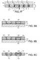
- the materialmay not adhere to the adhesion layer ( figure 8A ); on the contrary, it can interact too strongly with the adhesion layer and so there may be miscibility ( Figure 8B ).
- Figure 8Bone or more zones of narrowing 113 ( figure 8A ) or zones 123 for mixing the material 103 and adhesive 122 ( figure 8B ).
- these cases of miscibility or dewettingcan lead to tearing of the coating material, or components, the appearance of significant stresses on the wafer or the poor strength of the components.
- Step a)may include the positioning of one or more components in one or more cavities passing through a host matrix.
- the formation of the buffer layer during step b)is performed at least on the rear face of the matrix and the flanks of the cavity or cavities. buffer layer that does not completely fill the space between the sidewall of the cavities and the sidewall of the components, and separating, at the end of stage c), the material for coating the material of the host matrix.
- a method according to the inventionmay further comprise a thinning step of the rear face of the wafer.
- the component (s)has / have a substrate, for example mainly made of silicon, or AsGa, or InP or glass.
- a substratefor example mainly made of silicon, or AsGa, or InP or glass.
- each componentmay be of different size and type of dimensions or type of other components integrated in the same wafer.
- the buffer layermay be PMDA-DAH or PMDA EAD or PMDA ODA or PMDA DNB, or poly-V3D3, or an organic mineral resin or parylene C or parylene N or parylene D.
- the coating materialmay be epoxy or polyurethane or elastomeric or silicone or acrylic or methacrylate or polypropylene or fusible glass or fuse glass mixed with silica particles.
- the devicefurther comprises a buffer layer 6, present at least on the sides 5 and 5 'of the components and on the face 8 of the device.
- a buffer layer 6present at least on the sides 5 and 5 'of the components and on the face 8 of the device.
- This buffer layeris of thickness e.
- the thickness eis chosen so that it does not completely fill the space between two components.
- eis smaller than 0.1 times w, width of this space.
- a coating material 3different from the material of the buffer layer, is present, separated from the components 4 and 4 'and the face 8 of the device by the buffer layer 6.
- a coating material 3different from the material of the buffer layer, is present, separated from the components 4 and 4 'and the face 8 of the device by the buffer layer 6.
- One or more of the components 4may be chosen from various types of microelectronic components, for example each may be an integrated circuit, and / or a MEMS or NEMS sensor, and / or an optical component (MOEMS or NOEMS) and / or a biocomponent and / or a switch, and / or a component serving solely as conductive passage between the two faces of the device. These components may all be identical or different from each other (they may in particular have different thicknesses from each other).
- the face 8can then be treated by microelectronic or "above-IC” methods, as explained below.
- the figure 3illustrates a third embodiment of the invention wherein the various discrete components 4, 4 'and 4 "are arranged in one or more cavities 7 and 7' made inside a matrix 2, of thickness h. It is noted that it is possible to have several components in the same cavity (this is the case of the two components 4, 4 'of the figure 3 ).
- the front face 11 of the die 2is flush with the face 8 of the device, and is therefore approximately the same level as the faces 10, 10 'and 10''of the components 4.
- the host matrixis made of a material of which the CTE is identical or similar to that of the discrete components. It is for example a semiconductor material, such as silicon.
- the flanks of the cavities 7are covered by the layer buffer 6 whose thickness e is chosen so that it does not completely fill the spaces between two components and the gaps between the edges of the cavities 7 and the edges 5, 5 'or 5''of the components.
- eis smaller than 0.1 times w and w ', respective widths of these intervals.
- any devicecomprising at least one component 4, a buffer layer 6 and a coating material 3, obtained by combining all or part of the 3 embodiments described above.
- the component (s) 4 and 4 'are placed on a rigid and plane support 21, which is, for example, a support substrate made of silicon, or glass, or a quartz mask or a plate of alumina or polymer ( Figure 5A ).
- this substratehas a CTE close to or even identical to that of the components 4 in order to ensure good positioning of the components (thus limiting the displacements and / or stresses at the time of hardening of the coating material 3 (made for example by heating around 200 ° C)).
- a thickness e of buffer layer 6is then deposited with a high degree of conformity ( Figure 5B ).
- This buffer layer 6covers the rear face and the sides 5 of the component (s) 4, 4 ', as well as the substrate 21 (or any adhesive layer 22).
- the buffer layerhas a low Young's modulus advantageously between 1.5 GPa and 10 GPa.
- this buffer layerpreferably has a glass transition temperature Tg (6) less than the glass transition temperature Tg (3) of the coating material 3.
- Tg (6)is for example between 80 ° C and 150 ° C, the coating materials 3 generally having a glass transition temperature of between 120 ° C and 220 ° C.
- a method according to a second embodiment of the inventionis presented in connection with the Figures 7A-7F . This process makes it possible, among other things, to implement the device of the figure 3 .
- the wafercan be reintroduced into a microelectronic type line for "Above IC" steps, for example of the type already described above.
Landscapes
- Engineering & Computer Science (AREA)
- Computer Hardware Design (AREA)
- Microelectronics & Electronic Packaging (AREA)
- Power Engineering (AREA)
- Physics & Mathematics (AREA)
- Condensed Matter Physics & Semiconductors (AREA)
- General Physics & Mathematics (AREA)
- Manufacturing & Machinery (AREA)
- Micromachines (AREA)
- Formation Of Insulating Films (AREA)
Abstract
Description
Translated fromFrenchL'invention concerne le domaine de l'assemblage de microsystèmes ou de nanosystèmes à l'échelle d'une plaquette, par exemple en matériau semi-conducteur, tel que du silicium.The invention relates to the field of the assembly of microsystems or nanosystems at the scale of a wafer, for example of semiconductor material, such as silicon.
Elle concerne notamment les applications pour lesquelles sont recherchées des technologies d'intégration à haute densité de composants passifs, de détecteurs ou composants optoélectroniques ou de MEMS ou de NEMS directement sur les circuits, communément appelées "Above IC".It relates in particular to applications for which high density integration technologies for passive components, sensors or optoelectronic components or MEMS or NEMS directly on the circuits, commonly known as "Above IC" are sought.
Actuellement, les procédés d'intégration hétérogène ne peuvent se faire que sur des plaquettes de silicium entières. Les procédés " Above IC " sont donc limités aux domaines où l'intégrateur du microsystème peut disposer de plaquettes, ce qui implique des coûts importants en termes de jeu de masques et de fabrication des plaquettes chez un fondeur.Currently, heterogeneous integration processes can only be performed on whole silicon wafers. "Above IC" processes are therefore limited to areas where the integrator of the microsystem can have platelets, which involves significant costs in terms of mask set and manufacture of platelets in a foundry.
De plus, pour les applications comme la téléphonie, la surface active des circuits intégrés n'est pas suffisante pour y accueillir tous les éléments nécessaires au système (composant passifs, amplificateurs, switch, composants SAW ou BAW), ce qui est en particulier dû au fait que le rendement diminue quand la complexité des puces augmente. Il est donc nécessaire d'assembler post fabrication les différents éléments sur des substrats de type PCB (circuit imprimé) ou céramique. Les architectures sont souvent complexes et l'assemblage et l'interconnexion nécessitent beaucoup d'opérations individuelles (placement des composants et câblage filaire).In addition, for applications such as telephony, the active surface of the integrated circuits is not sufficient to accommodate all the elements necessary for the system (passive components, amplifiers, switches, SAW components or BAW), which is particularly due the fact that the yield decreases as the complexity of the chips increases. It is therefore necessary to assemble post manufacturing the different elements on substrates like PCB (printed circuit) or ceramic. Architectures are often complex and assembly and interconnection require a lot of individual operations (component placement and wired cabling).
Il existe une autre technique permettant l'intégration de nombreuses fonctionnalités sur une même puce, tout en ayant de bons rendements. Dans cette technique on reconstitue une plaquette à partir de puces discrètes disposés sur une plaquette support puis en les scellant avec un matériau d'enrobage et en éliminant la plaquette support. Cette plaquette reconstituée permet de procéder à des intégrations de type « above IC », mélangeant des composants provenant de plusieurs sources et assemblés dans un format adapté aux outils de dépôt disponible pour l'industriel. De plus, cette technique permet de réaliser des dispositifs complexes, contenant des composants fabriqués sur des substrats différents, en ne choisissant que des composants fonctionnels.There is another technique that allows the integration of many features on the same chip, while having good returns. In this technique, a wafer is reconstituted from discrete chips arranged on a support wafer and then sealed with a coating material and eliminating the support wafer. This reconstituted wafer makes it possible to carry out integrations of the "above IC" type, mixing components coming from several sources and assembled in a format adapted to the depositing tools available for the industrialist. Moreover, this technique makes it possible to produce complex devices, containing components manufactured on different substrates, by choosing only functional components.
Cette technique, dans laquelle on colle temporairement les faces actives des composants sur un adhésif, puis on les enrobe et on réalise un reroutage par-dessus, a été publiée en
On connaît également, dans ce type de technique, les procédés décrits dans les documents
Enfin, selon une autre méthode, décrite dans le document
Cette couche d'enrobage peut présenter trois types de défauts illustrés dans les
Tout d'abord, lors du dépôt du matériau d'enrobage, le matériau peut ne pas adhérer à la couche d'adhérence (
Des coefficients d'expansion thermique (CTE) différents entre, d'une part, la couche d'enrobage 103 (CTE proche de 10ppm/°C ou supérieur à cette valeur) et, d'autre part, les substrats de la plaquette d'accueil 102 et/ou des composants 104 (CTE voisin de 2,3 ppm/°C pour du silicium) induisent l'apparition de contraintes fortes dans la couche d'enrobage (
L'invention vise à résoudre ces problèmes.The invention aims to solve these problems.
Elle vise notamment à réduire l'impact de la différence de CTE sur les contraintes dans la plaquette.It aims in particular to reduce the impact of the CTE difference on the constraints in the wafer.
Un autre but de l'invention est d'améliorer l'interface entre le dispositif en cours de fabrication et la couche d'adhérence.Another object of the invention is to improve the interface between the device being manufactured and the adhesion layer.
L'invention concerne tout d'abord un dispositif électronique, ayant une face avant et une face arrière, muni d'au moins un composant discret intégré, la face active du composant apparaissant du coté de la face avant et comportant :
- un matériau d'enrobage, présent au moins latéralement par rapport au composant, assurant le maintient du dit composant dans le dispositif,
- une couche tampon, absente de la face active du composant, séparant le matériau d'enrobage du ou des composant(s).
- a coating material, present at least laterally with respect to the component, ensuring the maintenance of said component in the device,
- a buffer layer, absent from the active face of the component, separating the coating material from the component (s).
Dans le cas de deux composants voisins, la couche tampon ne remplit pas entièrement l'espace entre les composants, l'espace restant, entre les composants ou entre des portions de couche tampon présentes sur les flancs des composants, étant occupé par le matériau d'enrobage.In the case of two neighboring components, the buffer layer does not completely fill the space between the components, the remaining space between the components or between buffer layer portions present on the sidewalls of the components being occupied by the material. 'coating.
Dans un mode de réalisation, le ou les composant(s) est (sont) placé(s) dans au moins une cavité présente dans une matrice d'accueil, la ou les cavités traversant la matrice d'accueil, la couche tampon étant au moins présente sur les flancs de la ou des cavités. La couche tampon sépare ainsi le matériau d'enrobage du ou des composant(s) et de la matrice d'accueil, et est absente de la face avant de la matrice d'accueil. Elle ne remplit pas entièrement l'espace entre les flancs de la ou des cavités et les flancs des composants.In one embodiment, the component (s) is (are) placed in at least one cavity present in a host matrix, the cavity or cavities passing through the host matrix, the buffer layer being at least less present on the flanks of the cavity or cavities. The buffer layer thus separates the coating material from the component (s) and the host matrix, and is absent from the front face of the host matrix. It does not completely fill the space between the flanks of the cavity or cavities and the flanks of the components.
Quel que soit le mode de réalisation, la couche tampon a des propriétés lui permettant de limiter ou d'absorber les contraintes qui peuvent apparaître entre, d'une part, le matériau d'enrobage et, d'autre part, le ou les composants et l'éventuelle plaquette, lors de montées et/ou de descentes en températures.Whatever the embodiment, the buffer layer has properties enabling it to limit or absorb the stresses that may appear between, on the one hand, the coating material and, on the other hand, the component or components. and the eventual platelet, during climbs and / or descents at temperatures.
Selon deux variantes de chacun des dispositifs précédents :
- la couche tampon peut masquer le matériau d'enrobage sur la face avant du dispositif ;
- le matériau d'enrobage peut être apparent sur la face avant du dispositif, la couche tampon n'étant présente que sur les flancs du composant, le matériau d'enrobage et la couche tampon présentant un retrait par rapport à la surface active des composants.
- the buffer layer can mask the coating material on the front face of the device;
- the coating material may be visible on the front face of the device, the buffer layer being present only on the sidewalls of the component, the coating material and the buffer layer having a shrinkage relative to the active surface of the components.
L'invention concerne également un procédé d'intégration d'au moins un composant discret intégré en une plaquette, dite plaquette reconstituée, procédé dans lequel :
- a) on positionne au moins un composant discret sur un substrat, dit substrat support,
- b) puis on dépose une couche tampon au moins sur la face arrière et les flancs du composant, ladite couche tampon ne se déposant pas sur les surfaces en contact avec le substrat.
- c) ensuite on dépose un matériau d'enrobage au moins latéralement par rapport au composant, ce matériau étant déposé uniquement sur des surfaces recouvertes par la couche tampon.
- a) positioning at least one discrete component on a substrate, said support substrate,
- b) then depositing a buffer layer at least on the back side and the sides of the component, said buffer layer not being deposited on the surfaces in contact with the substrate.
- c) subsequently depositing a coating material at least laterally with respect to the component, this material being deposited only on surfaces covered by the buffer layer.
L'étape a) peut comporter le positionnement de un ou plusieurs composants dans une ou plusieurs cavités traversant une matrice d'accueil.Step a) may include the positioning of one or more components in one or more cavities passing through a host matrix.
La formation de la couche tampon lors de l'étape b) est réalisée au moins sur la face arrière de la matrice et les flancs de la ou des cavités, ladite couche tampon ne remplissant pas entièrement l'espace entre le flanc des cavités et le flanc des composants, et séparant, à l'issue de l'étape c), le matériau d'enrobage du matériau de la matrice d'accueil.The formation of the buffer layer during step b) is performed at least on the rear face of the matrix and the flanks of the cavity or cavities. buffer layer that does not completely fill the space between the sidewall of the cavities and the sidewall of the components, and separating, at the end of stage c), the material for coating the material of the host matrix.
La matrice peut être positionnée en premier sur le substrat support, puis les composants sont positionnés dans la ou les cavités de la matrice d'accueil. Inversement, la matrice peut n'être placée qu'une fois les composants discrets positionnés, la ou les cavités entourant les composants.The matrix may be positioned first on the support substrate, and then the components are positioned in the cavity (s) of the host matrix. Conversely, the matrix can be placed only once the discrete components are positioned, the cavity or cavities surrounding the components.
Le substrat support peut être en silicium, ou en verre, ou en alumine, ou en quartz ou en polymère.The support substrate may be silicon, or glass, or alumina, or quartz or polymer.
Un procédé selon l'invention peut comporter en outre une étape d'amincissement de la face arrière de la plaquette.A method according to the invention may further comprise a thinning step of the rear face of the wafer.
Un procédé selon l'invention peut comporter en outre une étape de collage en face arrière d'un substrat de renfort servant à assurer la tenue mécanique.A method according to the invention may further comprise a bonding step in the rear face of a reinforcing substrate for ensuring the mechanical strength.
Dans un procédé selon l'invention, une couche adhérente peut être déposée sur le substrat support préalablement à l'étape a), la couche tampon déposée en b) étant déposée sur au moins une partie du matériau adhérent non occupé par un composant, la face arrière et les flancs du ou des composant(s) et éventuellement sur le dos de la matrice d'accueil et les flancs des cavités.In a method according to the invention, an adherent layer may be deposited on the support substrate prior to step a), the buffer layer deposited in b) being deposited on at least a portion of the adherent material not occupied by a component, the rear face and the flanks of the component (s) and possibly on the back of the host matrix and the flanks of the cavities.
Dans un procédé selon l'invention la couche tampon adhère avantageusement à la couche d'adhérence et à la face arrière et aux flancs du ou des composant(s) et est préférentiellement non-miscible avec la couche adhérente. Ainsi, la couche tampon permet d'éviter la formation de matériau de réaction à la surface de la couche adhérente tout en maintenant les différents éléments sur le substrat support.In a process according to the invention, the buffer layer advantageously adheres to the adhesion layer and to the rear face and to the flanks of the component (s) and is preferentially immiscible with the adherent layer. Thus, the buffer layer avoids the formation of reaction material on the surface of the adherent layer while maintaining the various elements on the support substrate.
De plus, pour réduire les effets des contraintes la couche tampon, par exemple apparaissant dans la plaquette reconstituée lors de procédés d'intégration above IC ou lors du durcissement du matériau d'enrobage, a avantageusement une température de transition vitreuse inférieure à celle du matériau d'enrobage. Elle se déforme alors sous l'influence de contraintes en compression. Pour assurer sa déformation lors des variations négatives de températures, la couche tampon a aussi de préférence un module d'Young faible.In addition, to reduce the effects of stresses the buffer layer, for example appearing in the wafer reconstituted during integration processes above IC or during hardening of the coating material, advantageously has a glass transition temperature lower than that of the material. coating. It is then deformed under the influence of compressive stresses. To ensure its deformation during negative temperature variations, the buffer layer preferably also has a low Young's modulus.
Dans un procédé selon l'invention, la couche tampon peut être déposée en phase gazeuse, ou par ALD, ou par CVD, ou par procédé sol-gel.In a process according to the invention, the buffer layer can be deposited in the gas phase, or by ALD, or by CVD, or by sol-gel process.
Dans un procédé ou un dispositif selon l'invention, le ou les composant(s) a/ont un substrat par exemple principalement en silicium, ou en AsGa, ou en InP ou en verre. De plus, chaque composant peut être de dimensions et de type différents des dimensions ou type d'autres composants intégrés dans la même plaquette.In a method or a device according to the invention, the component (s) has / have a substrate, for example mainly made of silicon, or AsGa, or InP or glass. In addition, each component may be of different size and type of dimensions or type of other components integrated in the same wafer.
Chaque composant est par exemple du type composant électronique, ou MEMS ou NEMS, ou MOEMS ou NOEMS, ou bio-composant, ou composant passif ou composant servant au passage conducteur entre les faces avant et arrière du dispositif ou servant uniquement au passage conducteur entre les faces avant et arrière du dispositif.Each component is for example of the electronic component type, or MEMS or NEMS, or MOEMS or NOEMS, or bio-component, or passive component or component used for the conductive passage between the front and rear faces of the device or used only for conductive passage between the front and rear faces of the device.
La couche tampon a avantageusement une épaisseur comprise entre 10 nm et 10 µm.The buffer layer advantageously has a thickness of between 10 nm and 10 μm.
La couche tampon peut être en PMDA-DAH ou en PMDA EAD ou en PMDA ODA ou en PMDA DNB, ou en poly-V3D3, ou en une résine minérale organique ou en parylène C ou en parylène N ou en parylène D.The buffer layer may be PMDA-DAH or PMDA EAD or PMDA ODA or PMDA DNB, or poly-V3D3, or an organic mineral resin or parylene C or parylene N or parylene D.
Dans un procédé ou un dispositif selon l'invention, le matériau d'enrobage peut être de type époxy ou polyuréthane ou élastomère ou silicone ou acrylique ou méthacrylate ou polypropylène ou verre fusible ou de type verre fusible mélangé avec des particules de silice.In a method or a device according to the invention, the coating material may be epoxy or polyurethane or elastomeric or silicone or acrylic or methacrylate or polypropylene or fusible glass or fuse glass mixed with silica particles.
Dans un procédé ou un dispositif selon l'invention, dans le cas où il y a une matrice d'accueil avec des cavités, la matrice d'accueil peut être en silicium ou en AsGA ou en InP ou en verre. De plus, la surface de cette plaquette ou matrice d'accueil peut comporter un ou plusieurs composants semi-conducteurs parmi des composants électroniques, des MEMS ou des NEMS, des MOEMS ou des NOEMS, ou des bio-composants, ou des composants passifs.In a method or a device according to the invention, in the case where there is a host matrix with cavities, the host matrix may be silicon or AsGA or InP or glass. In addition, the surface of this wafer or host matrix may comprise one or more semiconductor components among electronic components, MEMS or NEMS, MOEMS or NOEMS, or bio-components, or passive components.
- Les
figures 1, 2 et 3 représentent des exemples de dispositifs selon l'invention,TheFigures 1, 2 and 3 represent examples of devices according to the invention, - la
figure 4 représente un des dispositifs selon l'invention sous la forme d'une plaquette reconstituée,thefigure 4 represents one of the devices according to the invention in the form of a reconstituted wafer, - les
figures 5A - 5F sont des étapes d'un exemple de mise en oeuvre d'un procédé selon l'invention,theFigures 5A - 5F are steps of an exemplary implementation of a method according to the invention, - la
figure 6 est un tableau reprenant les propriétés de matériaux proposés comme couche tampon dans le cadre de l'invention,thefigure 6 is a table showing the properties of materials proposed as buffer layer in the context of the invention, - les
figures 7A-7F sont des étapes d'un exemple de mise en oeuvre d'un deuxième procédé selon l'invention,theFigures 7A-7F are steps of an exemplary implementation of a second method according to the invention, - les
figures 8A-8C illustrent les problèmes identifiés par les inventeurs,theFigures 8A-8C illustrate the problems identified by the inventors, - la
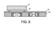
figure 9 illustre un exemple d'application d'un dispositif réalisé selon l'invention après passage dans une ligne de traitement above-IC.thefigure 9 illustrates an example of application of a device made according to the invention after passing through an above-IC processing line.
Des modes de réalisation de l'invention sont détaillés ci-dessous, illustrés par les
Un premier dispositif selon l'invention est représenté en coupe sur la
Ce dispositif comporte un ou plusieurs composants électroniques 4 et 4' d'épaisseur maximale h et de largeur L1. Les faces actives des composants sont désignées par les références 10 et 10': il s'agit des faces sur lesquelles sont réalisés les composants élémentaires définissant les fonctionnalités des composants. Les faces 10 et 10' affleurent la face 8, dite face avant du dispositif. Le dispositif suivant ce mode, mais également suivant les autres modes de réalisation, s'étend sensiblement dans un plan xy, son épaisseur h suivant la direction z, perpendiculaire au plan xOy étant petite par rapport à ses directions d'extension dans ce même plan xOy, l'épaisseur h pouvant aller de 10 µm ou de 300 µm à quelques millimètres, par exemple 1 mm ou 5 mm, les dimensions du dispositif dans le plan xOy pouvant aller de 150 mm à 400 mm ou même plus, notamment pour une dalle de verre.This device comprises one or more
Le dispositif comporte de plus une couche tampon6, présente au moins sur les flancs 5 et 5' des composants ainsi que sur la face 8 du dispositif. Dans cet exemple mais aussi dans les exemples qui suivent, on appelle flancs des composants des parties de ces composants qui sont sensiblement perpendiculaires au plan xOy du dispositif. Cette couche tampon est d'épaisseur e. Dans le cas où il y a plus de un composant, l'épaisseur e est choisie de telle sorte qu'elle ne remplisse pas intégralement l'espace situé entre deux composants. Avantageusement, e est plus petit que 0,1 fois w, largeur de cet espace.The device further comprises a
Enfin, un matériau d'enrobage 3, différent du matériau de la couche tampon, est présent, séparé des composants 4 et 4' et de la face 8 du dispositif par la couche tampon 6. Donc, entre deux composants, suivant un axe parallèle au plan de la surface 8 ou au plan xOy, hormis peut être pour une épaisseur e proche de la surface 8, deux composants sont séparés par au moins une première portion de couche tampon, une couche de matériau d'enrobage et une deuxième portion de couche tampon.Finally, a
Un ou plusieurs des composants 4 peut/peuvent être choisis parmi divers types de composants microélectroniques, par exemple chacun peut être un circuit intégré, et/ou un capteur MEMS ou NEMS, et/ou un composant optique (MOEMS ou NOEMS) et/ou un biocomposant et/ou un commutateur, et/ou un composant servant uniquement de passage conducteur entre les deux faces du dispositif. Ces composants peuvent être tous identiques ou être différents entre eux (ils peuvent notamment avoir des épaisseurs différentes les unes des autres).One or more of the
La face 8 peut ensuite être traitée par des procédés de type microélectronique ou « above-IC », comme expliqué ci-dessous.The
La couche tampon 6 a des propriétés lui permettant de limiter ou d'absorber les contraintes qui peuvent apparaître entre, d'une part, matériau d'enrobage et, d'autre part, le ou les composants et l'éventuelle plaquette, lors de montées et/ou de descentes en températures.The
Ainsi, cette couche tampon a, de préférence, un module d'Young bas, inférieur à celui de la résine d'enrobage. Ce module d'Young de la couche tampon est avantageusement compris entre 1,5 GPa et 10 GPa.Thus, this buffer layer preferably has a low Young's modulus, lower than that of the coating resin. This Young's modulus of the buffer layer is advantageously between 1.5 GPa and 10 GPa.
La couche tampon a, de préférence, une température de transition vitreuse Tg(6) inférieure à celle du matériau d'enrobage 3 Tg(3), par exemple comprise entre 80°C et 150°C (c'est le cas du parylène), les matériaux d'enrobage 3 - et notamment ceux donnés ici en exemple - ayant généralement une température de transition vitreuse comprise entre 120°C et 220°C.The buffer layer preferably has a glass transition temperature Tg (6) lower than that of the
A titre d'exemple, la couche tampon peut être en PMDA-DAH ou en PMDA EDA ou en PMDA ODA ou en PMDA-DNB ou en PMDA-PDA, ou en poly-V3D3 (il s'agit du poly(1,3,5-trivinyltrimethylcyclotrisiloxane)) ou en une résine minérale organique ou en parylène C ou en parylène N ou en parylène D. Avantageusement, la couche tampon 6 est en parylène C ou en parylène N ou en parylène D dont les propriétés sont données dans le tableau de la
Le matériau d'enrobage 3 a avantageusement un coefficient d'expansion thermique (CTE) bas, c'est - à - dire par exemple compris entre 5 ppm/°C et 50 ppm/°C, plus particulièrement inférieure à 20 ppm/°C.The
A titre d'exemple de matériau d'enrobage 3, on peut citer la résine époxy, le polyuréthane, l'élastomère, les matériaux silicones, l'acrylique, les méthacrylates, le polypropylène, ou un verre fusible. Pour diminuer le CTE de chacun de ces matériaux, il peut être choisi de les mélanger avec des particules, par exemple en silice, ou d'un autre type de matériau dans le but de conférer au matériau d'enrobage ainsi formé des propriétés électriques et/ou thermiques et/ou mécaniques.As an example of
La
La
Dans la matrice 2, deux cavités 7, 7' voisines peuvent être séparées par une distance désignée par L2, L1 désignant quant à elle la largeur d'un composant. Des ordres de grandeur pour les dimensions de h, L1 et L2 sont donnés plus loin.In the
Dans le mode de réalisation de la
La
Des exemples de matériaux pour la couche tampon et la couche d'enrobage du mode de réalisation des
Pour tous les exemples décrits ci-dessus, des ordres de grandeur pour les dimensions h, w, e, L1 et L2 peuvent être les suivants :
- h peut être compris entre 10 µm et quelques mm, il est par exemple de l'ordre de 5 mm,
- w et w' peuvent être compris entre 100 µm et quelques mm, ces valeurs sont par exemple de l'ordre de 1 mm,
- e peut être compris entre 10 nm et quelques µm, il est par exemple de l'ordre de 10 µm,
- L1 peut être compris entre 100 µm et quelques mm, par exemple de l'ordre de 2 cm,
- L2 peut être compris entre 100 µm et quelques mm, est par exemple de l'ordre de 2 cm,
- h may be between 10 μm and a few mm, it is for example of the order of 5 mm,
- w and w 'may be between 100 μm and a few mm, these values are for example of the order of 1 mm,
- e may be between 10 nm and some μm, it is for example of the order of 10 μm,
- L1 may be between 100 μm and a few mm, for example of the order of 2 cm,
- L2 may be between 100 μm and a few mm, for example of the order of 2 cm,
Ces valeurs sont des exemples et d'autres valeurs sont possibles en dehors des plages indiquées.These values are examples, and other values are possible outside the specified ranges.
Les dispositifs décrits en liaison avec les
- intégration de composants passifs en couche mince (résistances et/ou capacités et/ou inductances),
- et/ou reroutage de contacts électriques et/ou formation d'un ensemble complexe de pistes et de contacts entre les composants 4, 4' et 4''. Cet ensemble peut être composé d'empilements des matériaux métalliques et isolants, de façon à former par exemple des interconnexions (
couche 30 de lafigure 3 ), - et/ou intégration, sur la
surface 10 des composants 4, de composants optiques (par exemple de micro-lentilles) ou de plots d'interconnexion, par exemple par croissance de billes fusibles, ou transfert de billes, ou fabrication de "Stud Bump", ou croissance de micro-inserts, ou hybridation de composants sur la plaquette (Chip on Wafer).
- integration of thin film passive components (resistors and / or capacitors and / or inductors),
- and / or rerouting electrical contacts and / or forming a complex set of tracks and contacts between the
components layer 30 of thefigure 3 ) - and / or integrating, on the
surface 10 of thecomponents 4, optical components (for example micro-lenses) or interconnect pads, for example by growing fusible beads, or transfer of balls, or manufacturing of "Stud Bump ", or growth of micro-inserts, or hybridization of components on the wafer (Chip on Wafer).
Ces mêmes traitements peuvent être effectués sur tout dispositif, comportant au moins un composant 4, une couche tampon 6 et un matériau d'enrobage 3, obtenu en combinant tout ou partie des 3 modes de réalisation décrits précédemment.These same treatments can be performed on any device, comprising at least one
Un exemple de procédé selon l'invention va être donné, en liaison avec les
On procède au placement du ou des composants 4 et 4' sur un support 21 rigide et plan, qui est par exemple un substrat support en silicium, ou en verre, ou un masque en quartz ou une plaque d'alumine ou en polymère (
Les équipements de placement du ou des composants 4 permettent d'atteindre une précision latérale micronique, avec un parallélisme meilleur que 5.10-4 rad. Ces valeurs sont suffisantes pour reprendre, lors de l'intégration ultérieure sur la face 8, des contacts sur les plots de connexion des composants situés sur la face active et qui ont généralement une largeur de l'ordre de quelques dizaines de µm.The placement equipment of component (s) 4 makes it possible to reach a micron lateral precision, with parallelism better than 5.10-4 rad. These values are sufficient to resume, during the subsequent integration on the
La tenue temporaire du ou des composants sur le support 21 se fera de préférence grâce à une couche adhérente 22 déposée sur le support (
On positionne alors les composants avec leur face active 10 tournée vers le support 21 ou vers l'éventuelle couche d'adhérence 22 formée sur le support 21. L'alignement peut être réalisé grâce à des mires qui auront été réalisées au préalable sur le substrat support 21 ou sur la couche adhérente 22. Il y aura ainsi un espace X entre deux composants.The components are then positioned with their active face turned towards the
Une épaisseur e de couche tampon 6 est ensuite déposée avec une grande conformité (
Cette couche 6 est de préférence choisie pour ses qualités de mouillabilité et d'inertie chimique avec le matériau du substrat 21(et/ou l'éventuelle couche adhérente 22).This
Avantageusement, pour absorber les contraintes en tension et se déformer facilement lorsque la température diminue, la couche tampon a un module d'Young bas avantageusement compris entre 1,5 GPa et 10 GPa. A l'inverse, pour absorber les contraintes en compression lors des recuits, cette couche tampon a de préférence, une température de transition vitreuse Tg(6) inférieure à la température de transition vitreuse Tg(3) du matériau d'enrobage 3. Tg(6) est par exemple comprise entre 80°C et 150°C, les matériaux d'enrobage 3 ayant généralement une température de transition vitreuse comprise entre 120°C et 220°C.Advantageously, to absorb tension stresses and easily deform when the temperature decreases, the buffer layer has a low Young's modulus advantageously between 1.5 GPa and 10 GPa. Conversely, to absorb compression stresses during annealing, this buffer layer preferably has a glass transition temperature Tg (6) less than the glass transition temperature Tg (3) of the
L'épaisseur e de cette couche tampon 6 est choisie de telle sorte qu'elle ne remplisse pas intégralement les espaces X entre deux composants. Elle est par exemple choisie inférieure à 0,1 fois w, w désignant la largeur de l'espace X.The thickness e of this
Cette couche tampon 6 peut être déposée par ALD, par CVD, par procédé sol-gel ou en phase gazeuse, procédés qui sont adaptés aux épaisseurs recherchées. Avantageusement, la couche tampon 6 est en parylène C ou en parylène N ou en parylène D dont les propriétés sont données dans le tableau de la
On procède ensuite au remplissage, par le matériau 3 d'enrobage, de l'espace libre présent entre les composants 4, recouverts de la couche tampon 6 (
Un amincissement et un polissage de la face arrière 8' peuvent être ensuite réalisés (
Le dispositif peut être ensuite décollé du support 21 et de l'éventuelle couche d'adhérence 22 (
Il peut être envisagé, avant ou après l'étape de retrait du support 21, de coller la face arrière du dispositif sur un support de renfort 80 afin de rigidifier l'ensemble (
Il est ensuite possible de procéder sur la face avant 8 à un retrait d'une épaisseur e de la couche tampon 6, (
Ensuite le dispositif peut être introduit dans une ligne de type microélectronique pour les étapes «Above IC», par exemple du type déjà décrit ci-dessus.Then the device can be introduced into a microelectronic type line for "Above IC" steps, for example of the type already described above.
Un procédé selon un second mode de réalisation de l'invention est présenté en liaison avec les
On sélectionne (
On réalise dans cette plaquette (
On procède ensuite au placement des composants 4 dans les cavités 7 (
La tenue temporaire des composants et de la matrice d'accueil sur le support 21 pourra se faire grâce à une couche adhérente 22 déposée sur le support (
On positionne ensuite les composants avec leur face active 10 tournée vers le support 21 ou vers l'éventuelle couche d'adhérence 22 formée sur le support 21. L'alignement dans les cavités peut être réalisé grâce à des mires qui auront été réalisées au préalable, soit sur la matrice d'accueil2, soit sur le substrat support 21 ou sur la couche adhérente 22. En variante il est possible de disposer d'abord les composants sur le support 21 (ou sur la couche adhérente 22) et, ensuite, de rapporter la matrice d'accueil 2 autour des composants positionnés.The components are then positioned with their active face turned towards the
Il reste des espaces X et X' entre deux composants ou entre un composant et les flancs de la cavité qui l'entoure.There remain spaces X and X 'between two components or between a component and the flanks of the surrounding cavity.
Une couche tampon 6 est ensuite déposée avec une grande conformité (
L'épaisseur e de cette couche tampon est choisie de telle sorte qu'elle ne remplisse pas intégralement les cavités X et X'. Cette épaisseur est avantageusement inférieure à 0,1 fois (au moins 10 fois plus petite que) w', w' désignant la largeur de l'espace X', w' est du même ordre de grandeur que w, largeur de l'espace X.The thickness e of this buffer layer is chosen so that it does not completely fill the cavities X and X '. This thickness is advantageously less than 0.1 times (at least 10 times smaller than) w ', w' denoting the width of the space X ', w' is of the same order of magnitude as w, width of the space X.
On procède ensuite, dans chaque cavité 7, au remplissage de l'espace libre par le matériau d'enrobage 3 (
On peut ensuite procéder à des étapes de polissage face arrière et/ou de retrait du substrat support et/ou d'ajout d'un substrat de renfort (
La
Ensuite la plaquette peut être réintroduite dans une ligne de type microélectronique pour les étapes «Above IC», par exemple du type déjà décrit ci-dessus.Then the wafer can be reintroduced into a microelectronic type line for "Above IC" steps, for example of the type already described above.
Par rapport au procédé précédent, l'ajout d'une matrice d'accueil a l'avantage de présenter autour des composants 4 une surface sur laquelle une intégration de composants microélectroniques et/ou MEMS/NEMS peut déjà avoir été effectuée. Ainsi ce procédé réalisant l'invention permet non seulement de créer un dispositif multi-composant mais de créer des dispositifs de type « system in chip » dans lequel le ou les composants peuvent subir une intégration de type « above -IC » simultanée avec l'intégration des composants présents initialement sur la matrice d'accueil, évitant ainsi une surépaisseur de connections.Compared to the previous method, the addition of a host matrix has the advantage of having around the components 4 a surface on which integration of microelectronic components and / or MEMS / NEMS may already have been performed. Thus, this method embodying the invention makes it possible not only to create a multi-component device but to create "system in chip" type devices in which the component (s) can undergo a "above-IC" type integration simultaneously with the device. integration of the components present initially on the host matrix, thus avoiding a thickening of connections.
Comme le présente les
Le procédé illustré par les
Par rapport aux technologies d'assemblage conventionnelles de composants dans une plaquette (technique dite « Chip In Wafer »), les procédés selon l'invention, grâce aux propriétés physique de la couche tampon, permettent de minimiser les contraintes dans le matériau de remplissage qui peuvent courber les plaquettes. De plus, ces procédés facilitent l'industrialisation du procédé en éliminant les risques de miscibilité ou de mauvaise mouillabilité entre le matériau d'enrobage 3 et la couche d'adhérence.Compared to conventional assembly technologies of components in a wafer ("Chip In Wafer" technique), the methods according to the invention, thanks to the physical properties of the buffer layer, make it possible to minimize the stresses in the filling material which can bend platelets. In addition, these processes facilitate the industrialization of the process by eliminating the risks of miscibility or poor wettability between the
Enfin, un procédé selon l'invention permet de mixer des composants 4 déjà testés (« Known Good Die »), de sources et d'épaisseurs différentes dans une même matrice 2. Il est par exemple possible d'intégrer des composants servant uniquement de passage conducteur entre les deux faces de la matrice.Finally, a method according to the invention makes it possible to mix
La
Par-dessus cette couche 30 à été déposé au moins un composant électronique 40 pouvant être du même type que les composants insérés dans la plaquette reconstituée. Ce ou ces composants supérieurs 40 sont fixés au moyen d'éléments de connexion de type billes fusibles 45, Micro inserts, stud-bump, polymère conducteurs etc....On top of this
Claims (15)
Translated fromFrenchApplications Claiming Priority (1)
| Application Number | Priority Date | Filing Date | Title |
|---|---|---|---|
| FR0854944AFR2934082B1 (en) | 2008-07-21 | 2008-07-21 | MULTI-COMPONENT DEVICE INTEGRATED IN A MATRIX |
Publications (2)
| Publication Number | Publication Date |
|---|---|
| EP2148366A1true EP2148366A1 (en) | 2010-01-27 |
| EP2148366B1 EP2148366B1 (en) | 2019-05-01 |
Family
ID=40506434
Family Applications (1)
| Application Number | Title | Priority Date | Filing Date |
|---|---|---|---|
| EP09165564.7AActiveEP2148366B1 (en) | 2008-07-21 | 2009-07-15 | Device having plurality of integrated circuits in a matrix |
Country Status (4)
| Country | Link |
|---|---|
| US (1) | US8466568B2 (en) |
| EP (1) | EP2148366B1 (en) |
| JP (1) | JP2010098295A (en) |
| FR (1) | FR2934082B1 (en) |
Families Citing this family (12)
| Publication number | Priority date | Publication date | Assignee | Title |
|---|---|---|---|---|
| FR2917234B1 (en)* | 2007-06-07 | 2009-11-06 | Commissariat Energie Atomique | MULTI-COMPONENT DEVICE INTEGRATED IN A SEMICONDUCTOR MATRIX |
| FR2947948B1 (en)* | 2009-07-09 | 2012-03-09 | Commissariat Energie Atomique | HANDLE PLATE HAVING VISUALIZATION WINDOWS |
| US8772087B2 (en)* | 2009-10-22 | 2014-07-08 | Infineon Technologies Ag | Method and apparatus for semiconductor device fabrication using a reconstituted wafer |
| WO2011090717A1 (en) | 2009-12-28 | 2011-07-28 | Gvd Corporation | Coating methods, systems, and related articles |
| FR2974942B1 (en)* | 2011-05-06 | 2016-07-29 | 3D Plus | PROCESS FOR PRODUCING RECONSTITUTED PLATES WITH THE MAINTENANCE OF CHIPS DURING THEIR ENCAPSULATION |
| US9202963B2 (en)* | 2012-11-21 | 2015-12-01 | Taiwan Semiconductor Manufacturing Company, Ltd. | Dual-side illumination image sensor chips and methods for forming the same |
| US9530762B2 (en) | 2014-01-10 | 2016-12-27 | Taiwan Semiconductor Manufacturing Company Limited | Semiconductor package, semiconductor device and method of forming the same |
| US20150303171A1 (en)* | 2014-04-22 | 2015-10-22 | Cirrus Logic, Inc. | Systems and methods for carrying singulated device packages |
| SG11201906443UA (en)* | 2017-01-20 | 2019-08-27 | Mitsui Chemicals Tohcello Inc | Adhesive film and method for manufacturing electronic apparatus |
| FR3084204B1 (en) | 2018-07-18 | 2021-05-14 | Commissariat Energie Atomique | PROCESS FOR INTEGRATING STRUCTURES INTO A SUPPORT AND ASSOCIATED DEVICE |
| GB2582388A (en)* | 2019-03-22 | 2020-09-23 | Cirrus Logic Int Semiconductor Ltd | Composite structures |
| GB2582383A (en)* | 2019-03-22 | 2020-09-23 | Cirrus Logic Int Semiconductor Ltd | Semiconductor structures |
Citations (13)
| Publication number | Priority date | Publication date | Assignee | Title |
|---|---|---|---|---|
| GB2202673A (en) | 1987-03-26 | 1988-09-28 | Haroon Ahmed | Multiplechip assembly |
| US5353195A (en)* | 1993-07-09 | 1994-10-04 | General Electric Company | Integral power and ground structure for multi-chip modules |
| US5353498A (en) | 1993-02-08 | 1994-10-11 | General Electric Company | Method for fabricating an integrated circuit module |
| US6154366A (en)* | 1999-11-23 | 2000-11-28 | Intel Corporation | Structures and processes for fabricating moisture resistant chip-on-flex packages |
| DE19907295C1 (en)* | 1999-02-22 | 2001-02-08 | Univ Dresden Tech | Electronic and/or optical component mounting method for rear side of flexible printed circuit board has molded material used for encasing components on front side of circuit board before inversion of latter |
| FR2857157A1 (en) | 2003-07-01 | 2005-01-07 | 3D Plus Sa | METHOD FOR INTERCONNECTING ACTIVE AND PASSIVE COMPONENTS AND HETEROGENEOUS COMPONENT WITH LOW THICKNESS THEREFROM |
| FR2864342A1 (en) | 2003-12-19 | 2005-06-24 | 3D Plus Sa | Electronic components e.g. ball grid array type encapsulation packages, connecting method, involves connecting conducting zones of external outputs of components appearing on wafer`s connection surface |
| US6998533B2 (en)* | 2002-04-11 | 2006-02-14 | Koninklijke Philips Electronics N.V. | Electronic device and method of manufacturing same |
| US20060051895A1 (en)* | 2003-03-25 | 2006-03-09 | Fujitsu Limited | Method for manufacturing electronic component-mounted board |
| US20060220222A1 (en)* | 2005-03-29 | 2006-10-05 | Zhao-Chong Zeng | Chip embedded package structure and fabrication method thereof |
| US20070080458A1 (en)* | 2005-10-11 | 2007-04-12 | Tsuyoshi Ogawa | Hybrid module and method of manufacturing the same |
| US20070108610A1 (en)* | 2005-11-02 | 2007-05-17 | Hiroshi Kondo | Embedded semiconductor device substrate and production method thereof |
| US20080142946A1 (en)* | 2006-12-13 | 2008-06-19 | Advanced Chip Engineering Technology Inc. | Wafer level package with good cte performance |
Family Cites Families (25)
| Publication number | Priority date | Publication date | Assignee | Title |
|---|---|---|---|---|
| US4322980A (en) | 1979-11-08 | 1982-04-06 | Hitachi, Ltd. | Semiconductor pressure sensor having plural pressure sensitive diaphragms and method |
| JPS59188947A (en)* | 1983-04-11 | 1984-10-26 | Matsushita Electronics Corp | Manufacture of resin sealed type semiconductor device |
| ES8700500A1 (en) | 1984-02-17 | 1986-11-16 | American Telephone & Telegraph | Integrated circuit chip assembly. |
| US6379998B1 (en) | 1986-03-12 | 2002-04-30 | Hitachi, Ltd. | Semiconductor device and method for fabricating the same |
| US4958216A (en) | 1987-03-23 | 1990-09-18 | Kyocera Corporation | Package for housing semiconductor elements |
| GB2224600B (en) | 1988-10-29 | 1992-03-18 | Stc Plc | Circuit assembly |
| US5904502A (en) | 1997-09-04 | 1999-05-18 | International Business Machines Corporation | Multiple 3-dimensional semiconductor device processing method and apparatus |
| US6224711B1 (en)* | 1998-08-25 | 2001-05-01 | International Business Machines Corporation | Assembly process for flip chip package having a low stress chip and resulting structure |
| SE515032C2 (en) | 1998-09-09 | 2001-06-05 | Ericsson Telefon Ab L M | Electronic device comprising a component carrier as well as such component carrier and a method of manufacturing the device |
| US6982478B2 (en) | 1999-03-26 | 2006-01-03 | Oki Electric Industry Co., Ltd. | Semiconductor device and method of fabricating the same |
| JP2001024312A (en)* | 1999-07-13 | 2001-01-26 | Taiyo Yuden Co Ltd | Manufacture of electronic device, the electronic device, and method for filling resin |
| AU2001272814A1 (en)* | 2000-07-25 | 2002-02-05 | Chan-Ik Park | Plastic package base, air cavity type package and their manufacturing methods |
| US6706553B2 (en)* | 2001-03-26 | 2004-03-16 | Intel Corporation | Dispensing process for fabrication of microelectronic packages |
| JP2002368028A (en)* | 2001-06-13 | 2002-12-20 | Nec Corp | Semiconductor package and manufacturing method thereof |
| DE10239866B3 (en)* | 2002-08-29 | 2004-04-08 | Infineon Technologies Ag | Production of a semiconductor component used in circuit boards comprises forming electrical contact surfaces together within a smaller contacting region as the whole surface of the front side of the chip and further processing |
| SG143932A1 (en)* | 2003-05-30 | 2008-07-29 | Micron Technology Inc | Packaged microelectronic devices and methods of packaging microelectronic devices |
| WO2004112136A1 (en) | 2003-06-12 | 2004-12-23 | Koninklijke Philips Electronics N.V. | Electronic device |
| DE102004010956B9 (en) | 2004-03-03 | 2010-08-05 | Infineon Technologies Ag | Semiconductor device with a thin semiconductor chip and a rigid wiring substrate and method for the production and further processing of thin semiconductor chips |
| TWI256095B (en)* | 2004-03-11 | 2006-06-01 | Siliconware Precision Industries Co Ltd | Wafer level semiconductor package with build-up layer and process for fabricating the same |
| JP4381860B2 (en) | 2004-03-24 | 2009-12-09 | 日東電工株式会社 | Method and apparatus for separating reinforcing plate fixed to reinforced semiconductor wafer |
| DE102005024431B4 (en) | 2005-05-24 | 2009-08-06 | Infineon Technologies Ag | Process for the production of semiconductor devices using a carrier plate with double-sided adhesive film |
| US7768113B2 (en) | 2005-05-26 | 2010-08-03 | Volkan Ozguz | Stackable tier structure comprising prefabricated high density feedthrough |
| US7176567B2 (en)* | 2005-07-06 | 2007-02-13 | Advanced Chip Engineering Technology Inc. | Semiconductor device protective structure and method for fabricating the same |
| TWI283462B (en)* | 2005-09-27 | 2007-07-01 | Via Tech Inc | Bumpless chip package and fabricating process thereof |
| US7906860B2 (en)* | 2007-10-26 | 2011-03-15 | Infineon Technologies Ag | Semiconductor device |
- 2008
- 2008-07-21FRFR0854944Apatent/FR2934082B1/ennot_activeExpired - Fee Related
- 2009
- 2009-07-15EPEP09165564.7Apatent/EP2148366B1/enactiveActive
- 2009-07-16JPJP2009168270Apatent/JP2010098295A/enactivePending
- 2009-07-17USUS12/505,385patent/US8466568B2/enactiveActive
Patent Citations (14)
| Publication number | Priority date | Publication date | Assignee | Title |
|---|---|---|---|---|
| GB2202673A (en) | 1987-03-26 | 1988-09-28 | Haroon Ahmed | Multiplechip assembly |
| US5353498A (en) | 1993-02-08 | 1994-10-11 | General Electric Company | Method for fabricating an integrated circuit module |
| US5497033A (en) | 1993-02-08 | 1996-03-05 | Martin Marietta Corporation | Embedded substrate for integrated circuit modules |
| US5353195A (en)* | 1993-07-09 | 1994-10-04 | General Electric Company | Integral power and ground structure for multi-chip modules |
| DE19907295C1 (en)* | 1999-02-22 | 2001-02-08 | Univ Dresden Tech | Electronic and/or optical component mounting method for rear side of flexible printed circuit board has molded material used for encasing components on front side of circuit board before inversion of latter |
| US6154366A (en)* | 1999-11-23 | 2000-11-28 | Intel Corporation | Structures and processes for fabricating moisture resistant chip-on-flex packages |
| US6998533B2 (en)* | 2002-04-11 | 2006-02-14 | Koninklijke Philips Electronics N.V. | Electronic device and method of manufacturing same |
| US20060051895A1 (en)* | 2003-03-25 | 2006-03-09 | Fujitsu Limited | Method for manufacturing electronic component-mounted board |
| FR2857157A1 (en) | 2003-07-01 | 2005-01-07 | 3D Plus Sa | METHOD FOR INTERCONNECTING ACTIVE AND PASSIVE COMPONENTS AND HETEROGENEOUS COMPONENT WITH LOW THICKNESS THEREFROM |
| FR2864342A1 (en) | 2003-12-19 | 2005-06-24 | 3D Plus Sa | Electronic components e.g. ball grid array type encapsulation packages, connecting method, involves connecting conducting zones of external outputs of components appearing on wafer`s connection surface |
| US20060220222A1 (en)* | 2005-03-29 | 2006-10-05 | Zhao-Chong Zeng | Chip embedded package structure and fabrication method thereof |
| US20070080458A1 (en)* | 2005-10-11 | 2007-04-12 | Tsuyoshi Ogawa | Hybrid module and method of manufacturing the same |
| US20070108610A1 (en)* | 2005-11-02 | 2007-05-17 | Hiroshi Kondo | Embedded semiconductor device substrate and production method thereof |
| US20080142946A1 (en)* | 2006-12-13 | 2008-06-19 | Advanced Chip Engineering Technology Inc. | Wafer level package with good cte performance |
Non-Patent Citations (1)
| Title |
|---|
| CHANG-LEE CHEN ET AL.: "Bond Wireless Multipchip packaging Technology for High Speed Circuits", IEEE TRANSACTIONS ON COMPONENT HYBRIDS AND MANUFACTURING TECHNOLOGY, vol. 15, no. 4, pages 451 - 456, XP000311384 |
Also Published As
| Publication number | Publication date |
|---|---|
| US8466568B2 (en) | 2013-06-18 |
| JP2010098295A (en) | 2010-04-30 |
| US20100047567A1 (en) | 2010-02-25 |
| FR2934082B1 (en) | 2011-05-27 |
| EP2148366B1 (en) | 2019-05-01 |
| FR2934082A1 (en) | 2010-01-22 |
Similar Documents
| Publication | Publication Date | Title |
|---|---|---|
| EP2148366B1 (en) | Device having plurality of integrated circuits in a matrix | |
| EP2162907B1 (en) | Device including components embedded in cavities of a receptor plate and corresponding method | |
| EP0638933B1 (en) | Interconnection process of stacked semi-conductors chips and devices | |
| EP1651560B1 (en) | Stacked structure and production method thereof | |
| EP1634685A2 (en) | Thin electronic chip in glass for electronic component and manufacturing process | |
| WO2021099713A1 (en) | Method for manufacturing a functional chip suitable for being assembled to wire elements | |
| FR2823012A1 (en) | METHOD FOR THE SELECTIVE TRANSFER OF AT LEAST ONE ELEMENT FROM AN INITIAL MEDIUM TO A FINAL MEDIUM | |
| FR2929864A1 (en) | SELF-ASSEMBLY OF CHIPS ON A SUBSTRATE | |
| JP2007173811A (en) | IC matching substrate / carrier coupling structure, method of manufacturing the same, and method of manufacturing electronic device | |
| EP2829511A2 (en) | Device comprising a fluid channel having at least one micro or nanoelectronic system and method for producing such a device | |
| EP1825510A1 (en) | Method for collectively producing a superimposed element microstructure | |
| WO2006043000A2 (en) | Method for transferring at least one micrometer or millimetre-sized object by means of a polymer handle | |
| EP2406815B1 (en) | Method for positioning chips during the production of a reconstituted board | |
| FR2888402A1 (en) | METHOD FOR ASSEMBLING SUBSTRATES BY DEPOSITING A THIN OXIDE OR NITRIDE BONDING LAYER AND STRUCTURE THUS ASSEMBLED | |
| EP2798667B1 (en) | Method for manufacturing a multilayer structure on a substrate | |
| EP2162908B1 (en) | Reconstituted electronic device fabrication process and corresponding reconstituted electronic device | |
| WO2013098530A1 (en) | Method for manufacturing a multilayer structure on a substrate | |
| FR2809533A1 (en) | Monolithic microsystem with mosaic of components and manufacturing method, for use in microelectronics | |
| EP2040291A1 (en) | Method of gluing chips to a constraint substrate and method of placing a semi-conductor reading circuit under constraint | |
| FR2800198A1 (en) | Protection procedure for Integrated circuit chip, uses vacuum suction to spread insulating material between supporting layers holding chips | |
| WO2003032383A2 (en) | Method for making a thin layer comprising all or part of component(s) and/or of circuit(s) | |
| FR2848023A1 (en) | Insulation of a chip by the wire deposition of an insulating material into some tracks for the partial individualization by thinning, notably for an electronic device incorporating a number of interfaces |
Legal Events
| Date | Code | Title | Description |
|---|---|---|---|
| PUAI | Public reference made under article 153(3) epc to a published international application that has entered the european phase | Free format text:ORIGINAL CODE: 0009012 | |
| AK | Designated contracting states | Kind code of ref document:A1 Designated state(s):AT BE BG CH CY CZ DE DK EE ES FI FR GB GR HR HU IE IS IT LI LT LU LV MC MK MT NL NO PL PT RO SE SI SK SM TR | |
| AX | Request for extension of the european patent | Extension state:AL BA RS | |
| RAP1 | Party data changed (applicant data changed or rights of an application transferred) | Owner name:COMMISSARIAT A L'ENERGIE ATOMIQUE ET AUX ENERGIES | |
| 17P | Request for examination filed | Effective date:20100331 | |
| 17Q | First examination report despatched | Effective date:20101201 | |
| GRAP | Despatch of communication of intention to grant a patent | Free format text:ORIGINAL CODE: EPIDOSNIGR1 | |
| STAA | Information on the status of an ep patent application or granted ep patent | Free format text:STATUS: GRANT OF PATENT IS INTENDED | |
| RIC1 | Information provided on ipc code assigned before grant | Ipc:H01L 23/31 20060101ALI20181030BHEP Ipc:H01L 23/00 20060101ALI20181030BHEP Ipc:H01L 21/683 20060101ALI20181030BHEP Ipc:H01L 21/68 20060101ALI20181030BHEP Ipc:H01L 23/538 20060101AFI20181030BHEP | |
| INTG | Intention to grant announced | Effective date:20181129 | |
| GRAS | Grant fee paid | Free format text:ORIGINAL CODE: EPIDOSNIGR3 | |
| GRAA | (expected) grant | Free format text:ORIGINAL CODE: 0009210 | |
| STAA | Information on the status of an ep patent application or granted ep patent | Free format text:STATUS: THE PATENT HAS BEEN GRANTED | |
| AK | Designated contracting states | Kind code of ref document:B1 Designated state(s):AT BE BG CH CY CZ DE DK EE ES FI FR GB GR HR HU IE IS IT LI LT LU LV MC MK MT NL NO PL PT RO SE SI SK SM TR | |
| REG | Reference to a national code | Ref country code:GB Ref legal event code:FG4D Free format text:NOT ENGLISH | |
| REG | Reference to a national code | Ref country code:CH Ref legal event code:EP Ref country code:AT Ref legal event code:REF Ref document number:1128077 Country of ref document:AT Kind code of ref document:T Effective date:20190515 | |
| REG | Reference to a national code | Ref country code:DE Ref legal event code:R096 Ref document number:602009058089 Country of ref document:DE | |
| REG | Reference to a national code | Ref country code:IE Ref legal event code:FG4D Free format text:LANGUAGE OF EP DOCUMENT: FRENCH | |
| REG | Reference to a national code | Ref country code:NL Ref legal event code:MP Effective date:20190501 | |
| REG | Reference to a national code | Ref country code:LT Ref legal event code:MG4D | |
| PG25 | Lapsed in a contracting state [announced via postgrant information from national office to epo] | Ref country code:FI Free format text:LAPSE BECAUSE OF FAILURE TO SUBMIT A TRANSLATION OF THE DESCRIPTION OR TO PAY THE FEE WITHIN THE PRESCRIBED TIME-LIMIT Effective date:20190501 Ref country code:NO Free format text:LAPSE BECAUSE OF FAILURE TO SUBMIT A TRANSLATION OF THE DESCRIPTION OR TO PAY THE FEE WITHIN THE PRESCRIBED TIME-LIMIT Effective date:20190801 Ref country code:LT Free format text:LAPSE BECAUSE OF FAILURE TO SUBMIT A TRANSLATION OF THE DESCRIPTION OR TO PAY THE FEE WITHIN THE PRESCRIBED TIME-LIMIT Effective date:20190501 Ref country code:NL Free format text:LAPSE BECAUSE OF FAILURE TO SUBMIT A TRANSLATION OF THE DESCRIPTION OR TO PAY THE FEE WITHIN THE PRESCRIBED TIME-LIMIT Effective date:20190501 Ref country code:HR Free format text:LAPSE BECAUSE OF FAILURE TO SUBMIT A TRANSLATION OF THE DESCRIPTION OR TO PAY THE FEE WITHIN THE PRESCRIBED TIME-LIMIT Effective date:20190501 Ref country code:ES Free format text:LAPSE BECAUSE OF FAILURE TO SUBMIT A TRANSLATION OF THE DESCRIPTION OR TO PAY THE FEE WITHIN THE PRESCRIBED TIME-LIMIT Effective date:20190501 Ref country code:SE Free format text:LAPSE BECAUSE OF FAILURE TO SUBMIT A TRANSLATION OF THE DESCRIPTION OR TO PAY THE FEE WITHIN THE PRESCRIBED TIME-LIMIT Effective date:20190501 Ref country code:PT Free format text:LAPSE BECAUSE OF FAILURE TO SUBMIT A TRANSLATION OF THE DESCRIPTION OR TO PAY THE FEE WITHIN THE PRESCRIBED TIME-LIMIT Effective date:20190901 | |
| PG25 | Lapsed in a contracting state [announced via postgrant information from national office to epo] | Ref country code:BG Free format text:LAPSE BECAUSE OF FAILURE TO SUBMIT A TRANSLATION OF THE DESCRIPTION OR TO PAY THE FEE WITHIN THE PRESCRIBED TIME-LIMIT Effective date:20190801 Ref country code:GR Free format text:LAPSE BECAUSE OF FAILURE TO SUBMIT A TRANSLATION OF THE DESCRIPTION OR TO PAY THE FEE WITHIN THE PRESCRIBED TIME-LIMIT Effective date:20190802 Ref country code:LV Free format text:LAPSE BECAUSE OF FAILURE TO SUBMIT A TRANSLATION OF THE DESCRIPTION OR TO PAY THE FEE WITHIN THE PRESCRIBED TIME-LIMIT Effective date:20190501 | |
| REG | Reference to a national code | Ref country code:AT Ref legal event code:MK05 Ref document number:1128077 Country of ref document:AT Kind code of ref document:T Effective date:20190501 | |
| PG25 | Lapsed in a contracting state [announced via postgrant information from national office to epo] | Ref country code:IS Free format text:LAPSE BECAUSE OF FAILURE TO SUBMIT A TRANSLATION OF THE DESCRIPTION OR TO PAY THE FEE WITHIN THE PRESCRIBED TIME-LIMIT Effective date:20190901 | |
| PG25 | Lapsed in a contracting state [announced via postgrant information from national office to epo] | Ref country code:SK Free format text:LAPSE BECAUSE OF FAILURE TO SUBMIT A TRANSLATION OF THE DESCRIPTION OR TO PAY THE FEE WITHIN THE PRESCRIBED TIME-LIMIT Effective date:20190501 Ref country code:RO Free format text:LAPSE BECAUSE OF FAILURE TO SUBMIT A TRANSLATION OF THE DESCRIPTION OR TO PAY THE FEE WITHIN THE PRESCRIBED TIME-LIMIT Effective date:20190501 Ref country code:CZ Free format text:LAPSE BECAUSE OF FAILURE TO SUBMIT A TRANSLATION OF THE DESCRIPTION OR TO PAY THE FEE WITHIN THE PRESCRIBED TIME-LIMIT Effective date:20190501 Ref country code:DK Free format text:LAPSE BECAUSE OF FAILURE TO SUBMIT A TRANSLATION OF THE DESCRIPTION OR TO PAY THE FEE WITHIN THE PRESCRIBED TIME-LIMIT Effective date:20190501 Ref country code:EE Free format text:LAPSE BECAUSE OF FAILURE TO SUBMIT A TRANSLATION OF THE DESCRIPTION OR TO PAY THE FEE WITHIN THE PRESCRIBED TIME-LIMIT Effective date:20190501 Ref country code:AT Free format text:LAPSE BECAUSE OF FAILURE TO SUBMIT A TRANSLATION OF THE DESCRIPTION OR TO PAY THE FEE WITHIN THE PRESCRIBED TIME-LIMIT Effective date:20190501 | |
| REG | Reference to a national code | Ref country code:DE Ref legal event code:R097 Ref document number:602009058089 Country of ref document:DE | |
| PG25 | Lapsed in a contracting state [announced via postgrant information from national office to epo] | Ref country code:IT Free format text:LAPSE BECAUSE OF FAILURE TO SUBMIT A TRANSLATION OF THE DESCRIPTION OR TO PAY THE FEE WITHIN THE PRESCRIBED TIME-LIMIT Effective date:20190501 Ref country code:MC Free format text:LAPSE BECAUSE OF FAILURE TO SUBMIT A TRANSLATION OF THE DESCRIPTION OR TO PAY THE FEE WITHIN THE PRESCRIBED TIME-LIMIT Effective date:20190501 Ref country code:SM Free format text:LAPSE BECAUSE OF FAILURE TO SUBMIT A TRANSLATION OF THE DESCRIPTION OR TO PAY THE FEE WITHIN THE PRESCRIBED TIME-LIMIT Effective date:20190501 | |
| REG | Reference to a national code | Ref country code:CH Ref legal event code:PL | |
| PLBE | No opposition filed within time limit | Free format text:ORIGINAL CODE: 0009261 | |
| STAA | Information on the status of an ep patent application or granted ep patent | Free format text:STATUS: NO OPPOSITION FILED WITHIN TIME LIMIT | |
| PG25 | Lapsed in a contracting state [announced via postgrant information from national office to epo] | Ref country code:TR Free format text:LAPSE BECAUSE OF FAILURE TO SUBMIT A TRANSLATION OF THE DESCRIPTION OR TO PAY THE FEE WITHIN THE PRESCRIBED TIME-LIMIT Effective date:20190501 | |
| 26N | No opposition filed | Effective date:20200204 | |
| REG | Reference to a national code | Ref country code:BE Ref legal event code:MM Effective date:20190731 | |
| PG25 | Lapsed in a contracting state [announced via postgrant information from national office to epo] | Ref country code:PL Free format text:LAPSE BECAUSE OF FAILURE TO SUBMIT A TRANSLATION OF THE DESCRIPTION OR TO PAY THE FEE WITHIN THE PRESCRIBED TIME-LIMIT Effective date:20190501 | |
| PG25 | Lapsed in a contracting state [announced via postgrant information from national office to epo] | Ref country code:CH Free format text:LAPSE BECAUSE OF NON-PAYMENT OF DUE FEES Effective date:20190731 Ref country code:LU Free format text:LAPSE BECAUSE OF NON-PAYMENT OF DUE FEES Effective date:20190715 Ref country code:LI Free format text:LAPSE BECAUSE OF NON-PAYMENT OF DUE FEES Effective date:20190731 Ref country code:BE Free format text:LAPSE BECAUSE OF NON-PAYMENT OF DUE FEES Effective date:20190731 Ref country code:SI Free format text:LAPSE BECAUSE OF FAILURE TO SUBMIT A TRANSLATION OF THE DESCRIPTION OR TO PAY THE FEE WITHIN THE PRESCRIBED TIME-LIMIT Effective date:20190501 | |
| PG25 | Lapsed in a contracting state [announced via postgrant information from national office to epo] | Ref country code:IE Free format text:LAPSE BECAUSE OF NON-PAYMENT OF DUE FEES Effective date:20190715 | |
| PG25 | Lapsed in a contracting state [announced via postgrant information from national office to epo] | Ref country code:CY Free format text:LAPSE BECAUSE OF FAILURE TO SUBMIT A TRANSLATION OF THE DESCRIPTION OR TO PAY THE FEE WITHIN THE PRESCRIBED TIME-LIMIT Effective date:20190501 | |
| PG25 | Lapsed in a contracting state [announced via postgrant information from national office to epo] | Ref country code:HU Free format text:LAPSE BECAUSE OF FAILURE TO SUBMIT A TRANSLATION OF THE DESCRIPTION OR TO PAY THE FEE WITHIN THE PRESCRIBED TIME-LIMIT; INVALID AB INITIO Effective date:20090715 Ref country code:MT Free format text:LAPSE BECAUSE OF FAILURE TO SUBMIT A TRANSLATION OF THE DESCRIPTION OR TO PAY THE FEE WITHIN THE PRESCRIBED TIME-LIMIT Effective date:20190501 | |
| PG25 | Lapsed in a contracting state [announced via postgrant information from national office to epo] | Ref country code:MK Free format text:LAPSE BECAUSE OF FAILURE TO SUBMIT A TRANSLATION OF THE DESCRIPTION OR TO PAY THE FEE WITHIN THE PRESCRIBED TIME-LIMIT Effective date:20190501 | |
| PGFP | Annual fee paid to national office [announced via postgrant information from national office to epo] | Ref country code:DE Payment date:20240719 Year of fee payment:16 | |
| PGFP | Annual fee paid to national office [announced via postgrant information from national office to epo] | Ref country code:GB Payment date:20240722 Year of fee payment:16 | |
| PGFP | Annual fee paid to national office [announced via postgrant information from national office to epo] | Ref country code:FR Payment date:20240723 Year of fee payment:16 |