EP2138021B1 - Electrical connection of components - Google Patents
Electrical connection of componentsDownload PDFInfo
- Publication number
- EP2138021B1 EP2138021B1EP08718775AEP08718775AEP2138021B1EP 2138021 B1EP2138021 B1EP 2138021B1EP 08718775 AEP08718775 AEP 08718775AEP 08718775 AEP08718775 AEP 08718775AEP 2138021 B1EP2138021 B1EP 2138021B1
- Authority
- EP
- European Patent Office
- Prior art keywords
- sheet
- component
- resist layer
- etch resist
- contacts
- Prior art date
- Legal status (The legal status is an assumption and is not a legal conclusion. Google has not performed a legal analysis and makes no representation as to the accuracy of the status listed.)
- Not-in-force
Links
Images


Classifications
- H—ELECTRICITY
- H05—ELECTRIC TECHNIQUES NOT OTHERWISE PROVIDED FOR
- H05K—PRINTED CIRCUITS; CASINGS OR CONSTRUCTIONAL DETAILS OF ELECTRIC APPARATUS; MANUFACTURE OF ASSEMBLAGES OF ELECTRICAL COMPONENTS
- H05K1/00—Printed circuits
- H05K1/18—Printed circuits structurally associated with non-printed electric components
- H05K1/182—Printed circuits structurally associated with non-printed electric components associated with components mounted in the printed circuit board, e.g. insert mounted components [IMC]
- H05K1/185—Components encapsulated in the insulating substrate of the printed circuit or incorporated in internal layers of a multilayer circuit
- H05K1/188—Components encapsulated in the insulating substrate of the printed circuit or incorporated in internal layers of a multilayer circuit manufactured by mounting on or attaching to a structure having a conductive layer, e.g. a metal foil, such that the terminals of the component are connected to or adjacent to the conductive layer before embedding, and by using the conductive layer, which is patterned after embedding, at least partially for connecting the component
- G—PHYSICS
- G06—COMPUTING OR CALCULATING; COUNTING
- G06K—GRAPHICAL DATA READING; PRESENTATION OF DATA; RECORD CARRIERS; HANDLING RECORD CARRIERS
- G06K19/00—Record carriers for use with machines and with at least a part designed to carry digital markings
- G06K19/06—Record carriers for use with machines and with at least a part designed to carry digital markings characterised by the kind of the digital marking, e.g. shape, nature, code
- G06K19/067—Record carriers with conductive marks, printed circuits or semiconductor circuit elements, e.g. credit or identity cards also with resonating or responding marks without active components
- G06K19/07—Record carriers with conductive marks, printed circuits or semiconductor circuit elements, e.g. credit or identity cards also with resonating or responding marks without active components with integrated circuit chips
- G06K19/077—Constructional details, e.g. mounting of circuits in the carrier
- G06K19/07745—Mounting details of integrated circuit chips
- G06K19/07747—Mounting details of integrated circuit chips at least one of the integrated circuit chips being mounted as a module
- G—PHYSICS
- G06—COMPUTING OR CALCULATING; COUNTING
- G06K—GRAPHICAL DATA READING; PRESENTATION OF DATA; RECORD CARRIERS; HANDLING RECORD CARRIERS
- G06K19/00—Record carriers for use with machines and with at least a part designed to carry digital markings
- G06K19/06—Record carriers for use with machines and with at least a part designed to carry digital markings characterised by the kind of the digital marking, e.g. shape, nature, code
- G06K19/067—Record carriers with conductive marks, printed circuits or semiconductor circuit elements, e.g. credit or identity cards also with resonating or responding marks without active components
- G06K19/07—Record carriers with conductive marks, printed circuits or semiconductor circuit elements, e.g. credit or identity cards also with resonating or responding marks without active components with integrated circuit chips
- G06K19/077—Constructional details, e.g. mounting of circuits in the carrier
- G06K19/07749—Constructional details, e.g. mounting of circuits in the carrier the record carrier being capable of non-contact communication, e.g. constructional details of the antenna of a non-contact smart card
- G06K19/0775—Constructional details, e.g. mounting of circuits in the carrier the record carrier being capable of non-contact communication, e.g. constructional details of the antenna of a non-contact smart card arrangements for connecting the integrated circuit to the antenna
- H—ELECTRICITY
- H01—ELECTRIC ELEMENTS
- H01L—SEMICONDUCTOR DEVICES NOT COVERED BY CLASS H10
- H01L21/00—Processes or apparatus adapted for the manufacture or treatment of semiconductor or solid state devices or of parts thereof
- H01L21/02—Manufacture or treatment of semiconductor devices or of parts thereof
- H01L21/04—Manufacture or treatment of semiconductor devices or of parts thereof the devices having potential barriers, e.g. a PN junction, depletion layer or carrier concentration layer
- H01L21/50—Assembly of semiconductor devices using processes or apparatus not provided for in a single one of the groups H01L21/18 - H01L21/326 or H10D48/04 - H10D48/07 e.g. sealing of a cap to a base of a container
- H01L21/56—Encapsulations, e.g. encapsulation layers, coatings
- H—ELECTRICITY
- H01—ELECTRIC ELEMENTS
- H01L—SEMICONDUCTOR DEVICES NOT COVERED BY CLASS H10
- H01L23/00—Details of semiconductor or other solid state devices
- H01L23/48—Arrangements for conducting electric current to or from the solid state body in operation, e.g. leads, terminal arrangements ; Selection of materials therefor
- H01L23/482—Arrangements for conducting electric current to or from the solid state body in operation, e.g. leads, terminal arrangements ; Selection of materials therefor consisting of lead-in layers inseparably applied to the semiconductor body (electrodes)
- H01L23/4822—Beam leads
- H—ELECTRICITY
- H01—ELECTRIC ELEMENTS
- H01L—SEMICONDUCTOR DEVICES NOT COVERED BY CLASS H10
- H01L24/00—Arrangements for connecting or disconnecting semiconductor or solid-state bodies; Methods or apparatus related thereto
- H01L24/80—Methods for connecting semiconductor or other solid state bodies using means for bonding being attached to, or being formed on, the surface to be connected
- H01L24/81—Methods for connecting semiconductor or other solid state bodies using means for bonding being attached to, or being formed on, the surface to be connected using a bump connector
- H—ELECTRICITY
- H01—ELECTRIC ELEMENTS
- H01L—SEMICONDUCTOR DEVICES NOT COVERED BY CLASS H10
- H01L24/00—Arrangements for connecting or disconnecting semiconductor or solid-state bodies; Methods or apparatus related thereto
- H01L24/93—Batch processes
- H01L24/95—Batch processes at chip-level, i.e. with connecting carried out on a plurality of singulated devices, i.e. on diced chips
- H01L24/97—Batch processes at chip-level, i.e. with connecting carried out on a plurality of singulated devices, i.e. on diced chips the devices being connected to a common substrate, e.g. interposer, said common substrate being separable into individual assemblies after connecting
- H—ELECTRICITY
- H01—ELECTRIC ELEMENTS
- H01L—SEMICONDUCTOR DEVICES NOT COVERED BY CLASS H10
- H01L2224/00—Indexing scheme for arrangements for connecting or disconnecting semiconductor or solid-state bodies and methods related thereto as covered by H01L24/00
- H01L2224/01—Means for bonding being attached to, or being formed on, the surface to be connected, e.g. chip-to-package, die-attach, "first-level" interconnects; Manufacturing methods related thereto
- H01L2224/10—Bump connectors; Manufacturing methods related thereto
- H01L2224/15—Structure, shape, material or disposition of the bump connectors after the connecting process
- H01L2224/16—Structure, shape, material or disposition of the bump connectors after the connecting process of an individual bump connector
- H01L2224/161—Disposition
- H01L2224/16151—Disposition the bump connector connecting between a semiconductor or solid-state body and an item not being a semiconductor or solid-state body, e.g. chip-to-substrate, chip-to-passive
- H01L2224/16221—Disposition the bump connector connecting between a semiconductor or solid-state body and an item not being a semiconductor or solid-state body, e.g. chip-to-substrate, chip-to-passive the body and the item being stacked
- H01L2224/16225—Disposition the bump connector connecting between a semiconductor or solid-state body and an item not being a semiconductor or solid-state body, e.g. chip-to-substrate, chip-to-passive the body and the item being stacked the item being non-metallic, e.g. insulating substrate with or without metallisation
- H01L2224/16227—Disposition the bump connector connecting between a semiconductor or solid-state body and an item not being a semiconductor or solid-state body, e.g. chip-to-substrate, chip-to-passive the body and the item being stacked the item being non-metallic, e.g. insulating substrate with or without metallisation the bump connector connecting to a bond pad of the item
- H—ELECTRICITY
- H01—ELECTRIC ELEMENTS
- H01L—SEMICONDUCTOR DEVICES NOT COVERED BY CLASS H10
- H01L2224/00—Indexing scheme for arrangements for connecting or disconnecting semiconductor or solid-state bodies and methods related thereto as covered by H01L24/00
- H01L2224/01—Means for bonding being attached to, or being formed on, the surface to be connected, e.g. chip-to-package, die-attach, "first-level" interconnects; Manufacturing methods related thereto
- H01L2224/10—Bump connectors; Manufacturing methods related thereto
- H01L2224/15—Structure, shape, material or disposition of the bump connectors after the connecting process
- H01L2224/16—Structure, shape, material or disposition of the bump connectors after the connecting process of an individual bump connector
- H01L2224/161—Disposition
- H01L2224/16151—Disposition the bump connector connecting between a semiconductor or solid-state body and an item not being a semiconductor or solid-state body, e.g. chip-to-substrate, chip-to-passive
- H01L2224/16221—Disposition the bump connector connecting between a semiconductor or solid-state body and an item not being a semiconductor or solid-state body, e.g. chip-to-substrate, chip-to-passive the body and the item being stacked
- H01L2224/16245—Disposition the bump connector connecting between a semiconductor or solid-state body and an item not being a semiconductor or solid-state body, e.g. chip-to-substrate, chip-to-passive the body and the item being stacked the item being metallic
- H—ELECTRICITY
- H01—ELECTRIC ELEMENTS
- H01L—SEMICONDUCTOR DEVICES NOT COVERED BY CLASS H10
- H01L2224/00—Indexing scheme for arrangements for connecting or disconnecting semiconductor or solid-state bodies and methods related thereto as covered by H01L24/00
- H01L2224/01—Means for bonding being attached to, or being formed on, the surface to be connected, e.g. chip-to-package, die-attach, "first-level" interconnects; Manufacturing methods related thereto
- H01L2224/26—Layer connectors, e.g. plate connectors, solder or adhesive layers; Manufacturing methods related thereto
- H01L2224/28—Structure, shape, material or disposition of the layer connectors prior to the connecting process
- H01L2224/29—Structure, shape, material or disposition of the layer connectors prior to the connecting process of an individual layer connector
- H01L2224/29001—Core members of the layer connector
- H01L2224/29099—Material
- H01L2224/29198—Material with a principal constituent of the material being a combination of two or more materials in the form of a matrix with a filler, i.e. being a hybrid material, e.g. segmented structures, foams
- H01L2224/29199—Material of the matrix
- H01L2224/2929—Material of the matrix with a principal constituent of the material being a polymer, e.g. polyester, phenolic based polymer, epoxy
- H—ELECTRICITY
- H01—ELECTRIC ELEMENTS
- H01L—SEMICONDUCTOR DEVICES NOT COVERED BY CLASS H10
- H01L2224/00—Indexing scheme for arrangements for connecting or disconnecting semiconductor or solid-state bodies and methods related thereto as covered by H01L24/00
- H01L2224/01—Means for bonding being attached to, or being formed on, the surface to be connected, e.g. chip-to-package, die-attach, "first-level" interconnects; Manufacturing methods related thereto
- H01L2224/26—Layer connectors, e.g. plate connectors, solder or adhesive layers; Manufacturing methods related thereto
- H01L2224/28—Structure, shape, material or disposition of the layer connectors prior to the connecting process
- H01L2224/29—Structure, shape, material or disposition of the layer connectors prior to the connecting process of an individual layer connector
- H01L2224/29001—Core members of the layer connector
- H01L2224/29099—Material
- H01L2224/29198—Material with a principal constituent of the material being a combination of two or more materials in the form of a matrix with a filler, i.e. being a hybrid material, e.g. segmented structures, foams
- H01L2224/29298—Fillers
- H01L2224/29299—Base material
- H01L2224/293—Base material with a principal constituent of the material being a metal or a metalloid, e.g. boron [B], silicon [Si], germanium [Ge], arsenic [As], antimony [Sb], tellurium [Te] and polonium [Po], and alloys thereof
- H—ELECTRICITY
- H01—ELECTRIC ELEMENTS
- H01L—SEMICONDUCTOR DEVICES NOT COVERED BY CLASS H10
- H01L2224/00—Indexing scheme for arrangements for connecting or disconnecting semiconductor or solid-state bodies and methods related thereto as covered by H01L24/00
- H01L2224/73—Means for bonding being of different types provided for in two or more of groups H01L2224/10, H01L2224/18, H01L2224/26, H01L2224/34, H01L2224/42, H01L2224/50, H01L2224/63, H01L2224/71
- H01L2224/732—Location after the connecting process
- H01L2224/73201—Location after the connecting process on the same surface
- H01L2224/73203—Bump and layer connectors
- H01L2224/73204—Bump and layer connectors the bump connector being embedded into the layer connector
- H—ELECTRICITY
- H01—ELECTRIC ELEMENTS
- H01L—SEMICONDUCTOR DEVICES NOT COVERED BY CLASS H10
- H01L2224/00—Indexing scheme for arrangements for connecting or disconnecting semiconductor or solid-state bodies and methods related thereto as covered by H01L24/00
- H01L2224/80—Methods for connecting semiconductor or other solid state bodies using means for bonding being attached to, or being formed on, the surface to be connected
- H01L2224/81—Methods for connecting semiconductor or other solid state bodies using means for bonding being attached to, or being formed on, the surface to be connected using a bump connector
- H01L2224/8112—Aligning
- H01L2224/81121—Active alignment, i.e. by apparatus steering, e.g. optical alignment using marks or sensors
- H—ELECTRICITY
- H01—ELECTRIC ELEMENTS
- H01L—SEMICONDUCTOR DEVICES NOT COVERED BY CLASS H10
- H01L2224/00—Indexing scheme for arrangements for connecting or disconnecting semiconductor or solid-state bodies and methods related thereto as covered by H01L24/00
- H01L2224/80—Methods for connecting semiconductor or other solid state bodies using means for bonding being attached to, or being formed on, the surface to be connected
- H01L2224/81—Methods for connecting semiconductor or other solid state bodies using means for bonding being attached to, or being formed on, the surface to be connected using a bump connector
- H01L2224/818—Bonding techniques
- H01L2224/81801—Soldering or alloying
- H—ELECTRICITY
- H01—ELECTRIC ELEMENTS
- H01L—SEMICONDUCTOR DEVICES NOT COVERED BY CLASS H10
- H01L2224/00—Indexing scheme for arrangements for connecting or disconnecting semiconductor or solid-state bodies and methods related thereto as covered by H01L24/00
- H01L2224/80—Methods for connecting semiconductor or other solid state bodies using means for bonding being attached to, or being formed on, the surface to be connected
- H01L2224/83—Methods for connecting semiconductor or other solid state bodies using means for bonding being attached to, or being formed on, the surface to be connected using a layer connector
- H01L2224/8312—Aligning
- H01L2224/83121—Active alignment, i.e. by apparatus steering, e.g. optical alignment using marks or sensors
- H—ELECTRICITY
- H01—ELECTRIC ELEMENTS
- H01L—SEMICONDUCTOR DEVICES NOT COVERED BY CLASS H10
- H01L2224/00—Indexing scheme for arrangements for connecting or disconnecting semiconductor or solid-state bodies and methods related thereto as covered by H01L24/00
- H01L2224/80—Methods for connecting semiconductor or other solid state bodies using means for bonding being attached to, or being formed on, the surface to be connected
- H01L2224/83—Methods for connecting semiconductor or other solid state bodies using means for bonding being attached to, or being formed on, the surface to be connected using a layer connector
- H01L2224/838—Bonding techniques
- H01L2224/8385—Bonding techniques using a polymer adhesive, e.g. an adhesive based on silicone, epoxy, polyimide, polyester
- H01L2224/83851—Bonding techniques using a polymer adhesive, e.g. an adhesive based on silicone, epoxy, polyimide, polyester being an anisotropic conductive adhesive
- H—ELECTRICITY
- H01—ELECTRIC ELEMENTS
- H01L—SEMICONDUCTOR DEVICES NOT COVERED BY CLASS H10
- H01L2224/00—Indexing scheme for arrangements for connecting or disconnecting semiconductor or solid-state bodies and methods related thereto as covered by H01L24/00
- H01L2224/90—Methods for connecting semiconductor or solid state bodies using means for bonding not being attached to, or not being formed on, the body surface to be connected, e.g. pressure contacts using springs or clips
- H—ELECTRICITY
- H01—ELECTRIC ELEMENTS
- H01L—SEMICONDUCTOR DEVICES NOT COVERED BY CLASS H10
- H01L2224/00—Indexing scheme for arrangements for connecting or disconnecting semiconductor or solid-state bodies and methods related thereto as covered by H01L24/00
- H01L2224/93—Batch processes
- H01L2224/95—Batch processes at chip-level, i.e. with connecting carried out on a plurality of singulated devices, i.e. on diced chips
- H01L2224/97—Batch processes at chip-level, i.e. with connecting carried out on a plurality of singulated devices, i.e. on diced chips the devices being connected to a common substrate, e.g. interposer, said common substrate being separable into individual assemblies after connecting
- H—ELECTRICITY
- H01—ELECTRIC ELEMENTS
- H01L—SEMICONDUCTOR DEVICES NOT COVERED BY CLASS H10
- H01L24/00—Arrangements for connecting or disconnecting semiconductor or solid-state bodies; Methods or apparatus related thereto
- H01L24/01—Means for bonding being attached to, or being formed on, the surface to be connected, e.g. chip-to-package, die-attach, "first-level" interconnects; Manufacturing methods related thereto
- H01L24/10—Bump connectors ; Manufacturing methods related thereto
- H01L24/12—Structure, shape, material or disposition of the bump connectors prior to the connecting process
- H—ELECTRICITY
- H01—ELECTRIC ELEMENTS
- H01L—SEMICONDUCTOR DEVICES NOT COVERED BY CLASS H10
- H01L24/00—Arrangements for connecting or disconnecting semiconductor or solid-state bodies; Methods or apparatus related thereto
- H01L24/80—Methods for connecting semiconductor or other solid state bodies using means for bonding being attached to, or being formed on, the surface to be connected
- H01L24/83—Methods for connecting semiconductor or other solid state bodies using means for bonding being attached to, or being formed on, the surface to be connected using a layer connector
- H—ELECTRICITY
- H01—ELECTRIC ELEMENTS
- H01L—SEMICONDUCTOR DEVICES NOT COVERED BY CLASS H10
- H01L24/00—Arrangements for connecting or disconnecting semiconductor or solid-state bodies; Methods or apparatus related thereto
- H01L24/90—Methods for connecting semiconductor or solid state bodies using means for bonding not being attached to, or not being formed on, the body surface to be connected, e.g. pressure contacts using springs or clips
- H—ELECTRICITY
- H01—ELECTRIC ELEMENTS
- H01L—SEMICONDUCTOR DEVICES NOT COVERED BY CLASS H10
- H01L25/00—Assemblies consisting of a plurality of semiconductor or other solid state devices
- H01L25/16—Assemblies consisting of a plurality of semiconductor or other solid state devices the devices being of types provided for in two or more different subclasses of H10B, H10D, H10F, H10H, H10K or H10N, e.g. forming hybrid circuits
- H—ELECTRICITY
- H01—ELECTRIC ELEMENTS
- H01L—SEMICONDUCTOR DEVICES NOT COVERED BY CLASS H10
- H01L2924/00—Indexing scheme for arrangements or methods for connecting or disconnecting semiconductor or solid-state bodies as covered by H01L24/00
- H01L2924/01—Chemical elements
- H01L2924/01006—Carbon [C]
- H—ELECTRICITY
- H01—ELECTRIC ELEMENTS
- H01L—SEMICONDUCTOR DEVICES NOT COVERED BY CLASS H10
- H01L2924/00—Indexing scheme for arrangements or methods for connecting or disconnecting semiconductor or solid-state bodies as covered by H01L24/00
- H01L2924/01—Chemical elements
- H01L2924/01011—Sodium [Na]
- H—ELECTRICITY
- H01—ELECTRIC ELEMENTS
- H01L—SEMICONDUCTOR DEVICES NOT COVERED BY CLASS H10
- H01L2924/00—Indexing scheme for arrangements or methods for connecting or disconnecting semiconductor or solid-state bodies as covered by H01L24/00
- H01L2924/01—Chemical elements
- H01L2924/01013—Aluminum [Al]
- H—ELECTRICITY
- H01—ELECTRIC ELEMENTS
- H01L—SEMICONDUCTOR DEVICES NOT COVERED BY CLASS H10
- H01L2924/00—Indexing scheme for arrangements or methods for connecting or disconnecting semiconductor or solid-state bodies as covered by H01L24/00
- H01L2924/01—Chemical elements
- H01L2924/01019—Potassium [K]
- H—ELECTRICITY
- H01—ELECTRIC ELEMENTS
- H01L—SEMICONDUCTOR DEVICES NOT COVERED BY CLASS H10
- H01L2924/00—Indexing scheme for arrangements or methods for connecting or disconnecting semiconductor or solid-state bodies as covered by H01L24/00
- H01L2924/01—Chemical elements
- H01L2924/01023—Vanadium [V]
- H—ELECTRICITY
- H01—ELECTRIC ELEMENTS
- H01L—SEMICONDUCTOR DEVICES NOT COVERED BY CLASS H10
- H01L2924/00—Indexing scheme for arrangements or methods for connecting or disconnecting semiconductor or solid-state bodies as covered by H01L24/00
- H01L2924/01—Chemical elements
- H01L2924/01027—Cobalt [Co]
- H—ELECTRICITY
- H01—ELECTRIC ELEMENTS
- H01L—SEMICONDUCTOR DEVICES NOT COVERED BY CLASS H10
- H01L2924/00—Indexing scheme for arrangements or methods for connecting or disconnecting semiconductor or solid-state bodies as covered by H01L24/00
- H01L2924/01—Chemical elements
- H01L2924/01029—Copper [Cu]
- H—ELECTRICITY
- H01—ELECTRIC ELEMENTS
- H01L—SEMICONDUCTOR DEVICES NOT COVERED BY CLASS H10
- H01L2924/00—Indexing scheme for arrangements or methods for connecting or disconnecting semiconductor or solid-state bodies as covered by H01L24/00
- H01L2924/01—Chemical elements
- H01L2924/01033—Arsenic [As]
- H—ELECTRICITY
- H01—ELECTRIC ELEMENTS
- H01L—SEMICONDUCTOR DEVICES NOT COVERED BY CLASS H10
- H01L2924/00—Indexing scheme for arrangements or methods for connecting or disconnecting semiconductor or solid-state bodies as covered by H01L24/00
- H01L2924/01—Chemical elements
- H01L2924/01038—Strontium [Sr]
- H—ELECTRICITY
- H01—ELECTRIC ELEMENTS
- H01L—SEMICONDUCTOR DEVICES NOT COVERED BY CLASS H10
- H01L2924/00—Indexing scheme for arrangements or methods for connecting or disconnecting semiconductor or solid-state bodies as covered by H01L24/00
- H01L2924/01—Chemical elements
- H01L2924/01047—Silver [Ag]
- H—ELECTRICITY
- H01—ELECTRIC ELEMENTS
- H01L—SEMICONDUCTOR DEVICES NOT COVERED BY CLASS H10
- H01L2924/00—Indexing scheme for arrangements or methods for connecting or disconnecting semiconductor or solid-state bodies as covered by H01L24/00
- H01L2924/01—Chemical elements
- H01L2924/01072—Hafnium [Hf]
- H—ELECTRICITY
- H01—ELECTRIC ELEMENTS
- H01L—SEMICONDUCTOR DEVICES NOT COVERED BY CLASS H10
- H01L2924/00—Indexing scheme for arrangements or methods for connecting or disconnecting semiconductor or solid-state bodies as covered by H01L24/00
- H01L2924/01—Chemical elements
- H01L2924/01078—Platinum [Pt]
- H—ELECTRICITY
- H01—ELECTRIC ELEMENTS
- H01L—SEMICONDUCTOR DEVICES NOT COVERED BY CLASS H10
- H01L2924/00—Indexing scheme for arrangements or methods for connecting or disconnecting semiconductor or solid-state bodies as covered by H01L24/00
- H01L2924/013—Alloys
- H01L2924/014—Solder alloys
- H—ELECTRICITY
- H01—ELECTRIC ELEMENTS
- H01L—SEMICONDUCTOR DEVICES NOT COVERED BY CLASS H10
- H01L2924/00—Indexing scheme for arrangements or methods for connecting or disconnecting semiconductor or solid-state bodies as covered by H01L24/00
- H01L2924/06—Polymers
- H01L2924/078—Adhesive characteristics other than chemical
- H01L2924/07802—Adhesive characteristics other than chemical not being an ohmic electrical conductor
- H—ELECTRICITY
- H01—ELECTRIC ELEMENTS
- H01L—SEMICONDUCTOR DEVICES NOT COVERED BY CLASS H10
- H01L2924/00—Indexing scheme for arrangements or methods for connecting or disconnecting semiconductor or solid-state bodies as covered by H01L24/00
- H01L2924/10—Details of semiconductor or other solid state devices to be connected
- H01L2924/11—Device type
- H01L2924/12—Passive devices, e.g. 2 terminal devices
- H01L2924/1204—Optical Diode
- H01L2924/12041—LED
- H—ELECTRICITY
- H01—ELECTRIC ELEMENTS
- H01L—SEMICONDUCTOR DEVICES NOT COVERED BY CLASS H10
- H01L2924/00—Indexing scheme for arrangements or methods for connecting or disconnecting semiconductor or solid-state bodies as covered by H01L24/00
- H01L2924/10—Details of semiconductor or other solid state devices to be connected
- H01L2924/11—Device type
- H01L2924/12—Passive devices, e.g. 2 terminal devices
- H01L2924/1204—Optical Diode
- H01L2924/12042—LASER
- H—ELECTRICITY
- H01—ELECTRIC ELEMENTS
- H01L—SEMICONDUCTOR DEVICES NOT COVERED BY CLASS H10
- H01L2924/00—Indexing scheme for arrangements or methods for connecting or disconnecting semiconductor or solid-state bodies as covered by H01L24/00
- H01L2924/10—Details of semiconductor or other solid state devices to be connected
- H01L2924/11—Device type
- H01L2924/12—Passive devices, e.g. 2 terminal devices
- H01L2924/1204—Optical Diode
- H01L2924/12044—OLED
- H—ELECTRICITY
- H01—ELECTRIC ELEMENTS
- H01L—SEMICONDUCTOR DEVICES NOT COVERED BY CLASS H10
- H01L2924/00—Indexing scheme for arrangements or methods for connecting or disconnecting semiconductor or solid-state bodies as covered by H01L24/00
- H01L2924/10—Details of semiconductor or other solid state devices to be connected
- H01L2924/11—Device type
- H01L2924/14—Integrated circuits
- H—ELECTRICITY
- H01—ELECTRIC ELEMENTS
- H01L—SEMICONDUCTOR DEVICES NOT COVERED BY CLASS H10
- H01L2924/00—Indexing scheme for arrangements or methods for connecting or disconnecting semiconductor or solid-state bodies as covered by H01L24/00
- H01L2924/19—Details of hybrid assemblies other than the semiconductor or other solid state devices to be connected
- H01L2924/1901—Structure
- H01L2924/1904—Component type
- H01L2924/19041—Component type being a capacitor
- H—ELECTRICITY
- H01—ELECTRIC ELEMENTS
- H01L—SEMICONDUCTOR DEVICES NOT COVERED BY CLASS H10
- H01L2924/00—Indexing scheme for arrangements or methods for connecting or disconnecting semiconductor or solid-state bodies as covered by H01L24/00
- H01L2924/19—Details of hybrid assemblies other than the semiconductor or other solid state devices to be connected
- H01L2924/1901—Structure
- H01L2924/1904—Component type
- H01L2924/19042—Component type being an inductor
- H—ELECTRICITY
- H01—ELECTRIC ELEMENTS
- H01L—SEMICONDUCTOR DEVICES NOT COVERED BY CLASS H10
- H01L2924/00—Indexing scheme for arrangements or methods for connecting or disconnecting semiconductor or solid-state bodies as covered by H01L24/00
- H01L2924/19—Details of hybrid assemblies other than the semiconductor or other solid state devices to be connected
- H01L2924/1901—Structure
- H01L2924/1904—Component type
- H01L2924/19043—Component type being a resistor
- H—ELECTRICITY
- H05—ELECTRIC TECHNIQUES NOT OTHERWISE PROVIDED FOR
- H05K—PRINTED CIRCUITS; CASINGS OR CONSTRUCTIONAL DETAILS OF ELECTRIC APPARATUS; MANUFACTURE OF ASSEMBLAGES OF ELECTRICAL COMPONENTS
- H05K1/00—Printed circuits
- H05K1/18—Printed circuits structurally associated with non-printed electric components
- H05K1/189—Printed circuits structurally associated with non-printed electric components characterised by the use of a flexible or folded printed circuit
- H—ELECTRICITY
- H05—ELECTRIC TECHNIQUES NOT OTHERWISE PROVIDED FOR
- H05K—PRINTED CIRCUITS; CASINGS OR CONSTRUCTIONAL DETAILS OF ELECTRIC APPARATUS; MANUFACTURE OF ASSEMBLAGES OF ELECTRICAL COMPONENTS
- H05K2201/00—Indexing scheme relating to printed circuits covered by H05K1/00
- H05K2201/03—Conductive materials
- H05K2201/0332—Structure of the conductor
- H05K2201/0335—Layered conductors or foils
- H05K2201/0355—Metal foils
- H—ELECTRICITY
- H05—ELECTRIC TECHNIQUES NOT OTHERWISE PROVIDED FOR
- H05K—PRINTED CIRCUITS; CASINGS OR CONSTRUCTIONAL DETAILS OF ELECTRIC APPARATUS; MANUFACTURE OF ASSEMBLAGES OF ELECTRICAL COMPONENTS
- H05K2201/00—Indexing scheme relating to printed circuits covered by H05K1/00
- H05K2201/09—Shape and layout
- H05K2201/09009—Substrate related
- H05K2201/09118—Moulded substrate
- H—ELECTRICITY
- H05—ELECTRIC TECHNIQUES NOT OTHERWISE PROVIDED FOR
- H05K—PRINTED CIRCUITS; CASINGS OR CONSTRUCTIONAL DETAILS OF ELECTRIC APPARATUS; MANUFACTURE OF ASSEMBLAGES OF ELECTRICAL COMPONENTS
- H05K2201/00—Indexing scheme relating to printed circuits covered by H05K1/00
- H05K2201/10—Details of components or other objects attached to or integrated in a printed circuit board
- H05K2201/10613—Details of electrical connections of non-printed components, e.g. special leads
- H05K2201/10621—Components characterised by their electrical contacts
- H05K2201/10674—Flip chip
- H—ELECTRICITY
- H05—ELECTRIC TECHNIQUES NOT OTHERWISE PROVIDED FOR
- H05K—PRINTED CIRCUITS; CASINGS OR CONSTRUCTIONAL DETAILS OF ELECTRIC APPARATUS; MANUFACTURE OF ASSEMBLAGES OF ELECTRICAL COMPONENTS
- H05K2203/00—Indexing scheme relating to apparatus or processes for manufacturing printed circuits covered by H05K3/00
- H05K2203/14—Related to the order of processing steps
- H05K2203/1461—Applying or finishing the circuit pattern after another process, e.g. after filling of vias with conductive paste, after making printed resistors
- H05K2203/1469—Circuit made after mounting or encapsulation of the components
- H—ELECTRICITY
- H05—ELECTRIC TECHNIQUES NOT OTHERWISE PROVIDED FOR
- H05K—PRINTED CIRCUITS; CASINGS OR CONSTRUCTIONAL DETAILS OF ELECTRIC APPARATUS; MANUFACTURE OF ASSEMBLAGES OF ELECTRICAL COMPONENTS
- H05K3/00—Apparatus or processes for manufacturing printed circuits
- H05K3/02—Apparatus or processes for manufacturing printed circuits in which the conductive material is applied to the surface of the insulating support and is thereafter removed from such areas of the surface which are not intended for current conducting or shielding
- H05K3/06—Apparatus or processes for manufacturing printed circuits in which the conductive material is applied to the surface of the insulating support and is thereafter removed from such areas of the surface which are not intended for current conducting or shielding the conductive material being removed chemically or electrolytically, e.g. by photo-etch process
- H05K3/061—Etching masks
- H—ELECTRICITY
- H05—ELECTRIC TECHNIQUES NOT OTHERWISE PROVIDED FOR
- H05K—PRINTED CIRCUITS; CASINGS OR CONSTRUCTIONAL DETAILS OF ELECTRIC APPARATUS; MANUFACTURE OF ASSEMBLAGES OF ELECTRICAL COMPONENTS
- H05K3/00—Apparatus or processes for manufacturing printed circuits
- H05K3/10—Apparatus or processes for manufacturing printed circuits in which conductive material is applied to the insulating support in such a manner as to form the desired conductive pattern
- H05K3/20—Apparatus or processes for manufacturing printed circuits in which conductive material is applied to the insulating support in such a manner as to form the desired conductive pattern by affixing prefabricated conductor pattern
- H05K3/202—Apparatus or processes for manufacturing printed circuits in which conductive material is applied to the insulating support in such a manner as to form the desired conductive pattern by affixing prefabricated conductor pattern using self-supporting metal foil pattern
- Y—GENERAL TAGGING OF NEW TECHNOLOGICAL DEVELOPMENTS; GENERAL TAGGING OF CROSS-SECTIONAL TECHNOLOGIES SPANNING OVER SEVERAL SECTIONS OF THE IPC; TECHNICAL SUBJECTS COVERED BY FORMER USPC CROSS-REFERENCE ART COLLECTIONS [XRACs] AND DIGESTS
- Y10—TECHNICAL SUBJECTS COVERED BY FORMER USPC
- Y10T—TECHNICAL SUBJECTS COVERED BY FORMER US CLASSIFICATION
- Y10T29/00—Metal working
- Y10T29/49—Method of mechanical manufacture
- Y10T29/49002—Electrical device making
- Y10T29/49117—Conductor or circuit manufacturing
- Y10T29/49124—On flat or curved insulated base, e.g., printed circuit, etc.
- Y10T29/49126—Assembling bases
- Y—GENERAL TAGGING OF NEW TECHNOLOGICAL DEVELOPMENTS; GENERAL TAGGING OF CROSS-SECTIONAL TECHNOLOGIES SPANNING OVER SEVERAL SECTIONS OF THE IPC; TECHNICAL SUBJECTS COVERED BY FORMER USPC CROSS-REFERENCE ART COLLECTIONS [XRACs] AND DIGESTS
- Y10—TECHNICAL SUBJECTS COVERED BY FORMER USPC
- Y10T—TECHNICAL SUBJECTS COVERED BY FORMER US CLASSIFICATION
- Y10T29/00—Metal working
- Y10T29/49—Method of mechanical manufacture
- Y10T29/49002—Electrical device making
- Y10T29/49117—Conductor or circuit manufacturing
- Y10T29/49124—On flat or curved insulated base, e.g., printed circuit, etc.
- Y10T29/49128—Assembling formed circuit to base
- Y—GENERAL TAGGING OF NEW TECHNOLOGICAL DEVELOPMENTS; GENERAL TAGGING OF CROSS-SECTIONAL TECHNOLOGIES SPANNING OVER SEVERAL SECTIONS OF THE IPC; TECHNICAL SUBJECTS COVERED BY FORMER USPC CROSS-REFERENCE ART COLLECTIONS [XRACs] AND DIGESTS
- Y10—TECHNICAL SUBJECTS COVERED BY FORMER USPC
- Y10T—TECHNICAL SUBJECTS COVERED BY FORMER US CLASSIFICATION
- Y10T29/00—Metal working
- Y10T29/49—Method of mechanical manufacture
- Y10T29/49002—Electrical device making
- Y10T29/49117—Conductor or circuit manufacturing
- Y10T29/49124—On flat or curved insulated base, e.g., printed circuit, etc.
- Y10T29/4913—Assembling to base an electrical component, e.g., capacitor, etc.
- Y10T29/49131—Assembling to base an electrical component, e.g., capacitor, etc. by utilizing optical sighting device
- Y—GENERAL TAGGING OF NEW TECHNOLOGICAL DEVELOPMENTS; GENERAL TAGGING OF CROSS-SECTIONAL TECHNOLOGIES SPANNING OVER SEVERAL SECTIONS OF THE IPC; TECHNICAL SUBJECTS COVERED BY FORMER USPC CROSS-REFERENCE ART COLLECTIONS [XRACs] AND DIGESTS
- Y10—TECHNICAL SUBJECTS COVERED BY FORMER USPC
- Y10T—TECHNICAL SUBJECTS COVERED BY FORMER US CLASSIFICATION
- Y10T29/00—Metal working
- Y10T29/49—Method of mechanical manufacture
- Y10T29/49002—Electrical device making
- Y10T29/49117—Conductor or circuit manufacturing
- Y10T29/49124—On flat or curved insulated base, e.g., printed circuit, etc.
- Y10T29/4913—Assembling to base an electrical component, e.g., capacitor, etc.
- Y10T29/49144—Assembling to base an electrical component, e.g., capacitor, etc. by metal fusion
- Y—GENERAL TAGGING OF NEW TECHNOLOGICAL DEVELOPMENTS; GENERAL TAGGING OF CROSS-SECTIONAL TECHNOLOGIES SPANNING OVER SEVERAL SECTIONS OF THE IPC; TECHNICAL SUBJECTS COVERED BY FORMER USPC CROSS-REFERENCE ART COLLECTIONS [XRACs] AND DIGESTS
- Y10—TECHNICAL SUBJECTS COVERED BY FORMER USPC
- Y10T—TECHNICAL SUBJECTS COVERED BY FORMER US CLASSIFICATION
- Y10T29/00—Metal working
- Y10T29/49—Method of mechanical manufacture
- Y10T29/49002—Electrical device making
- Y10T29/49117—Conductor or circuit manufacturing
- Y10T29/49124—On flat or curved insulated base, e.g., printed circuit, etc.
- Y10T29/49147—Assembling terminal to base
Definitions
- This inventionrelates to a method of electrically connecting a component to an electrical circuit, and to the resulting circuitry.
- the inventionhas particular, but not exclusive, application to the manufacture of cards for RFID (radio frequency identification devices) and IC cards, so called smart cards, where a component such as an integrated circuit is attached to an antenna or other electrically conductive element.
- the basic components of an RFID chip or tag for an RFID cardcomprise a substrate (usually a plastic film or paper), a patterned conductive antenna and an integrated circuit which may store data and be interrogated.
- a substrateusually a plastic film or paper
- a patterned conductive antennaand an integrated circuit which may store data and be interrogated.
- the RFID industryis mainly driven by cost and significant advances have been made in reducing the cost of the chips which are used in RFID. A significant amount of work has also occurred in bringing down the cost of the antenna.
- the utilisation of additive metallization methods, printing and low-cost materialshave all contributed to a reduction in the cost of antenna production.
- a significant cost in the manufacture of the RFID cardstill comes from the process of attaching the chip to the antenna.
- the precision with which the chip must be placedrequires expensive and relatively slow equipment.
- RFID antennas and other electrical conductive elementsare traditionally manufactured by a process of masking and etching metal-covered substrates.
- a plastic or composite substratee.g. PET or FR4 epoxy composite
- the metal structurewould then be coated and patterned with an etch resistant material (e.g. photoresist) and then immersed in a chemical etchant (ferric chloride, nitric acid or a mixture of peroxide and sulphuric acid in the case of copper, hydrochloric acid or sodium hydroxide in the case of aluminium) to remove the excess metal foil.
- a chemical etchantferrric chloride, nitric acid or a mixture of peroxide and sulphuric acid in the case of copper, hydrochloric acid or sodium hydroxide in the case of aluminium
- the etch resistwould then be removed to leave a patterned metal layer in the form of an antenna.
- the RFID inlaywould then be completed by attaching an RFID chip to the antenna such that raised contact bumps on the surface of the chip come into electrical contact with contact pads at the feed points of the antenna. This may be done by first connecting these bumps to a larger metal structure (known as a strap or interposer) which is then bonded to the antenna, or by directly placing the chip face down on the antenna with the contact bumps on top of the contact pads. In either case, good electrical contact and mechanical bonding are achieved by the use of a conductive adhesive paste or film. In many cases this adhesive is anisotropically conductive (i.e. the conductivity in the lateral or in-plane direction is much lower than that in the vertical direction) so as to prevent shorting between the bumps.
- a conductive adhesive paste or filmis anisotropically conductive (i.e. the conductivity in the lateral or in-plane direction is much lower than that in the vertical direction) so as to prevent shorting between the bumps.
- the antenna itselfmay be fabricated using an additive patterning technique.
- the conductive regionis added patternwise (usually using a printing technique) to the insulating substrate. This may be done by printing a paste or suspension of metal particles such as silver or copper. Alternatively it may be achieved by printing a catalytic material which is then coated with metal using a process of electroless deposition. In either case the antenna conductivity may be further increased by subsequent electrolytic plating.
- the conducting materials in their chosen formare usually found to be far more costly than simple metal foils.
- aluminium foilis particularly abundant and available at significantly lower cost (per unit area) than the materials usually used for antenna manufacture. Consequently, some manufacturers choose to directly die-cut aluminium foil to form antennas. This method, although cheap, greatly limits the complexity of the antennas which may be formed and leads to great difficulties in the handling of the materials during subsequent processes.
- the cost of accurately locating the bumped pads of the chips to the contacts on the antennais also significant (in terms of process time and the capital equipment involved).
- the applicantshave demonstrated (e.g. in WO 2005/044451 ) the ability to place the chip relatively inaccurately with the contact pads facing upwards, and utilise the digital nature of inkjet printing to print the connection between the antenna and the contact bumps. Even so, this process still requires the fabrication of an antenna by either a traditional additive or subtractive method.
- the inventionemploys a different way of ensuring that there is accurate registration between the component and the electrical circuit to which it is to be electrically connected.
- US 2005/0070046discloses mounting electronic components to one side of a substrate with electrodes passing through the substrate, and forming a pattern of electrical connections to the electrodes on the opposed side of the substrate by photolithography.
- US 2005/0199929discloses a capacitor device in which components are mounted on one side of a copper foil, with an upper wiring pattern formed thereon, and a layer wiring pattern is formed in a resist film on the opposed side of the foil by photolithography.
- US 2005/0141150discloses a method of connecting a component to a circuit by depositing connection-forming material between contacts. Imaging techniques may be used to detect the position of the contacts prior to the deposition step.
- a method of electrically connecting a component to an electrical circuitcomprising forming an intermediate product in which the component is disposed on one side of an electrically conducting sheet so that at least one pair of contacts of the component are electrically connected by the sheet and in which a patterned etch resist layer is disposed on the other side of the sheet in registration with the component on said one side of the sheet, and then exposing the other side of the sheet to an etching agent and thereby removing areas of the sheet to leave the electrical circuit and also to remove the electrical interconnection between the contacts, wherein the patterned etch resist layer is applied to the other side of the sheet in the required registration by an optical system which locates the position at which the component is disposed on the sheet by locating indentations in the sheet produced by contact bumps on the component.
- the componentis disposed on said one side of the sheet and the etch resist layer accurately positioned on the other side, before the etching step takes place.
- the etch resist layermay be disposed on the other side of the sheet by a digital printing process, such as inkjet printing.
- the patterned etch resist layeris applied to the other side of the sheet in the required registration by an optical system which locates the position at which the component is disposed on the said one side of the sheet.
- the optical systemlocates indentations in the sheet produced by contact bumps on the component. This allows for the component to be disposed on said one side of the sheet relatively inaccurately because the optical system accurately positions the patterned etch resist layer with respect to the component.
- the intermediate productis formed by disposing the component on said one side of the sheet and then applying the patterned etch resist layer to the other side of the sheet.
- the intermediate productmay be formed by applying a further etch resist layer to said one side of the sheet and to the exposed surface of the component, and in this case the further etch resist layer may be applied to the one side of the sheet wholly or substantially covering the one side of the sheet so as to form a substrate.
- the further etch resist layer applied to said one side of the sheetmay have a pattern and may be exposed to a corresponding etching agent which removes areas of the sheet not covered by the etch resist layer on said one side of the sheet, whereby the electrical circuit is defined by pathways formed by etching from both sides of the sheet.
- the etch resist layersmay be made of the same etch resistant material and may be subjected simultaneously to the same etching agent, for example by dipping into the etching agent.
- the componentmay be an integrated circuit chip but may also be a resistor, inductor, or capacitor which could be printed directly onto the sheet.
- the sheetmay be made of any electrically conductive material, metal or non-metal, but is preferably aluminium foil because this is inexpensive and available in a readily useable form.
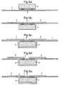
- a continuous electrically conducting sheet in the form of a metal foil 1has applied to a surface a patterned etch resist layer 2 defining an electrical circuit to be formed.
- a component in the form of a chip 3 with spaced contact pads 4is placed on the opposite side of the foil 1 such that the contact pads 4 make electrical contact with the foil 1 and register with the areas of the etch resist layer 2.
- the component side of the foil 1is completely coated with a second etch resist layer 5 which fills the region 6 between the pads 4 and thus forms an underfill.
- the resulting intermediate product of Figure 1dis then immersed in a chemical or other etch solution which dissolves the unprotected areas of foil so as to leave conductive regions 1' of the foil corresponding to the areas covered by the etch resist layer 2. Also, this etching process removes the metal foil between the contact pads 4 and thus breaks the electrical contact between the pads 4, as shown by the discontinuity 7 in the foil ( Figures 1e and 1f ).
- the etch resist layer 2may be left in place to form a substrate for the resulting device, or it may be stripped away ( Figure If).
- the application of the etch resist layer 2may be performed patternwise by a process such as analogue or digital printing (e.g. screen, flexo, gravure, inkjet printing or laser printing).
- the mask represented by the layer 2may be applied by a traditional photo lithographic method such as the application of a photo resist (dry film or liquid), subsequent exposure to light through a mask, followed by a developing stage.
- the chip 3may be secured to the metal foil 1 by using an adhesive which may be cured or allowed to set.
- the second etch resist layer 5may be used to completely flow around the chip and bond it to the substrate.
- a chemical etch materialmay be used to remove unprotected metal.
- other etching processessuch as electrochemical or plasma etching may also be used.
- plasma etchingthe process may be non-directional or directional, such as reactive ion etching.
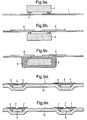
- Figure 2differs from Figure 1 in that the chip 3 is first placed in contact with one surface of the metal foil 1, and the patterned etch resistant layer 2 then applied to the other side of the foil.
- the chip sideis then completely coated with a second etch resist layer 5 to form the intermediate product ( Figure 2c ) identical to that of Figure 1d .
- the resulting productis then etched, Figure 2d , and the etch resist layer 2 may then be stripped away, as shown in Figure 2e .
- Figure 3shows a variation of the method of Figure 2 .
- the layer 2has several strips ( Figure 3b ) so the intermediate product appears as illustrated in Figure 3c .
- the resultis as shown in Figure 3e .
- the method of Figure 3is especially relevant to HF (13.56 MHz) RFID tags where the tag is usually in the form of a spiral and one of the major manufacturing problems is making a connection from the inside of the spiral to the outside without shorting the tracks in between.
- a chip on an interposercould be used to bridge the gap.
- An insulating adhesivemay also be used so as to insulate from the intermediate tracks. Failing that a metal strip with an insulating coating under it could also be used to bridge the gap.
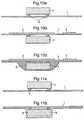
- the chip 3is first placed on the metal foil 1 ( Figure 4a ) after which the etch resist layer 5 is coated over the chip side of the foil ( Figure 4b ).
- the patterned etch resist layer 2is then applied to the opposite side of the foil ( Figure 4c ) to form the intermediate product which is then etched ( Figure 4d ), after which the patterned etch resist layer 2 may be stripped ( Figure 4e ).
- the chip 3is adhered to the metal foil 1 ( Figure 5a ) using an adhesive material 8.
- the layer 2is then applied ( Figure 5b ).
- the material 8may or may not be used as an etch resistant material which ensures that the area between the contact pads is completely filled.
- Figure 5crepresents the intermediate product which is then subjected to etching, Figure 5d , and then optional stripping of the patterned etch resist layer 2, as shown in Figure 5e .
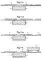
- the variation shown in Figure 6uses a conductive material 9 for adhering the chip pads 4 to the metal foil 1.
- the conductive material 9may be an electrically conductive paste or glue, solder or other electrically conductive material.
- the etch resist layer 2is then applied to the opposite side of the foil, as shown in Figure 6b , and after this the further etch resist layer 5 is applied to the chip side of the foil so as to cover the foil and the exposed areas of the chip.
- the intermediate product of Figure 6cis then etched, as previously described, the result being illustrated in Figure 6d .
- the chip 3is adhered to the foil 1 using an anisotropic conductive paste or an anisotropic conductive film 10.
- Thisis a material which comprises a binder layer and sparsely distributed conductive particles such that when the chip 3 is pressed into the film or paste 10 the particles are pressed together to make the film or paste conductive only in the vertical direction, or the direction of compression.
- Thishas the advantage that it ensures good electrical connection to the foil without causing short circuit between the contact pads 4.
- the patterned etch resist layer 2is then applied ( Figure 7b ) and the second etch resist layer 5 is applied ( Figure 7c ). This intermediate product is then etched to produce the product shown in Figure 7d .
- Figures 8a and 8bcorrespond to Figures 2a and 2b .
- Figure 8cshows how a plurality of chips 3 can be placed on the foil 1 to provide a plurality of devices.
- a second etch resist layer 12is then applied, Figure 8c , after which etching proceeds to give the result illustrated in Figure 8d .
- the second etch resist layer 12may be formed by a lamination process or by the deposition of a liquid which is then solidified or allowed to solidify. Also, the second etch resist material may be applied as a continuous layer or may be applied pattern wise such that the device substrates are also patterned or partially or fully singulated after the etching process.
- Figures 9a and 9brespectively correspond to Figures 8a and 8b .
- Figure 9cshows the second etch resist layer applied to the chip side of the foil and acting as an underfill
- Figure 9dillustrates how a further etch resist layer 12 may be laminated onto the structure, after which etching takes place to produce the result shown in Figure 9e .
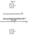
- Figure 10illustrates how certain contact pads 13 of the chip 3 are initially short circuited by the foil 1 and deliberately remain short circuited even after the etching process, as illustrated by Figure 10c .
- the chipalso has pads which are electrically isolated by the etching process, as in the preceding methods, and one such pad may be one of the pads 13.
- Figures 11a to 11ccorrespond to Figures 4a to 4c respectively, but it will be noted in Figure 11c that the etch resist layer 2 has further pathways so that after etching and stripping of the layer 2 one or more additional components 14 may be applied to the metal foil, thus providing a method of populating both sides of the metal foil with components, i.e. producing a buried component board.
- componentssuch as resistors, inductors or capacitors can be printed directly onto the foil. This applies to each of the foregoing examples.
- printable semiconductorssuch as conjugated polymers
- active componentssuch as thin film transistors, LEDs or memory elements can also be printed.
- the chip 3 and layer 2are disposed on the foil 1 in accurate registration by an optical system, for example as shown in Figure 12 or 13 .
- two cameras 15may be disposed on respective sides of a transparent platform 16.
- a calibration pattern 17 on a transparent substrate 18is used to ensure that both cameras 15 see an identical view (in terms of magnification and field of view) of the resist pattern.
- Computer softwaremay then be used to superimpose the images from the two cameras 15 such that the detail of both sides of the calibration pattern are visible on the same image at the same time.
- the image from one of the camerasmust be mirrored about one axis in order to achieve this and this is an option with the available software.
- this vision systemmay then be used to place a component on the upper side of the substrate in register with the pattern on the underside.
- the same camera systemmay be used to align a photo mask 19 with a photo resist layer in the situation where the chip 3 has been previously placed on a metal foil 1.
- this systemdescribes the procedure for placing components or aligning patterns by hand, it will be appreciated that machine vision technology could readily be used to automate such a system, i.e. such that components could be automatically placed relative to a pattern or such that a pattern could be formed (either by printing or lithographic means) in register with a pre-placed device.
- the process of digital printinge.g. inkjet printing, laser printing or laser direct imaging
- Formulation 2gave a slightly brittle film and a low viscosity fluid and so was modified with more oligomer (at the expense o the brittle IBOA)
- Inkjet printingis used (using two XaarJet 500/40 industrial inkjet printheads and associated drive electronics) to deposit the resist described in Formulation 3 onto a 10 micron thick copper foil. The image is then cured by passing it under a Light Hammer 6 UV lamp from Fusion Systems.
- the imageis deposited in the form of an antenna for Wireless Local Area Network communication at 2.45 GHz.
- the antennais formed of multiple isolated areas, so arranged such that surface mount capacitors and inductors may be placed on the pattern, bridging the gaps between the isolated areas.
- Two capacitors and an inductorare prepared for mounting by applying a small amount of a conductive epoxy resin (from ITW Chemtronics) on the contact pads at each end of each device.
- a conductive epoxy resinfrom ITW Chemtronics
- An insulating epoxy resin(Araldite Rapide - from Huntsman) is applied to each component, between the contact pads - this serves to further secure the device to the substrate but also to provide an insulating sealed region between the contact pads.
- the imaging system described in Figure 12is used to place the capacitors and inductor onto the reverse side of the metal foil such that they bridge the gaps in the printed resist pattern.
- the adhesivesare then cured in an oven at 60 °C for 2 hours.
- a further layer of epoxy resinis then applied across the whole of the component side of the foil.
- a layer of Melinex 339 PET film(from DuPont Teijin Films) is then laminated onto the epoxy. The whole device is then allowed to cure in the oven at 60 °C for a further 4 hours.
- the cured structureis then immersed in a solution of 10% sulphuric acid and 5% potassium persulfate at 50 °C until all the copper foil between the areas of resist has been etched away.
- a Clincher connector(From FCI) is then used to pierce the whole device structure and make external contact to the antenna for connection to the rest of the circuit.
- a UHF RFID chip from Texas Instrumentswas bonded to a 12 ⁇ m thick aluminium foil using and anisotropic conductive film IOB-3 from Betchcorp, Colorado.
- the chipwas pressed into the film using a pressure of 25 psi, on a hotplate at 50 °C and held in place for 5 seconds.
- the assembled devicewas then cured in an oven at 130 °C for 1 hour.
- the devicewas then placed chip-side-down on the sample stage of a DMP-2831 inkjet print system from Dimatix.
- the DMP-2831 systemincludes an integrated fiducial recognition camera which was then used to find the indentations produced in the aluminium foil by the contact bumps on the chip.
- the alignment software included with the DMP-2831was then used to print the image of a UHF RFID antenna such that the contact point of the antenna lined up with the indentations of the contact bumps.
- the imagewas printed using the resist formulation described above as Formulation 3.
- the resistwas cured during the print process using the output fibre of a fibre coupled UV lamp (Exfo) which was retrofitted to the cartridge mount of the DMP-2831.
- a Xaar Jet 500/80 print headwas then used to print a complete covering of the same resist ink on the reverse (chip) side of the aluminium foil. This was cured using a Light hammer 6 UV lamp from Fusion Systems.
- the resultwas a self supporting working RFID tag.
- an optical systemthat employs two cameras on respective sides of the sheet to achieve the required registration.
- At least one additional componentis disposed on the other surface of the sheet.
Landscapes
- Engineering & Computer Science (AREA)
- Microelectronics & Electronic Packaging (AREA)
- Computer Hardware Design (AREA)
- Physics & Mathematics (AREA)
- General Physics & Mathematics (AREA)
- Theoretical Computer Science (AREA)
- Power Engineering (AREA)
- Condensed Matter Physics & Semiconductors (AREA)
- Manufacturing & Machinery (AREA)
- Manufacturing Of Printed Circuit Boards (AREA)
- Coupling Device And Connection With Printed Circuit (AREA)
Abstract
Description
- This invention relates to a method of electrically connecting a component to an electrical circuit, and to the resulting circuitry. The invention has particular, but not exclusive, application to the manufacture of cards for RFID (radio frequency identification devices) and IC cards, so called smart cards, where a component such as an integrated circuit is attached to an antenna or other electrically conductive element.
- The basic components of an RFID chip or tag for an RFID card comprise a substrate (usually a plastic film or paper), a patterned conductive antenna and an integrated circuit which may store data and be interrogated. The RFID industry is mainly driven by cost and significant advances have been made in reducing the cost of the chips which are used in RFID. A significant amount of work has also occurred in bringing down the cost of the antenna. The utilisation of additive metallization methods, printing and low-cost materials have all contributed to a reduction in the cost of antenna production. However, a significant cost in the manufacture of the RFID card still comes from the process of attaching the chip to the antenna. As well as the need to form a conductive bond between the chip and antenna, the precision with which the chip must be placed requires expensive and relatively slow equipment.
- RFID antennas and other electrical conductive elements are traditionally manufactured by a process of masking and etching metal-covered substrates. For example, a plastic or composite substrate (e.g. PET or FR4 epoxy composite) is co-laminated with a copper or aluminium foil. The metal structure would then be coated and patterned with an etch resistant material (e.g. photoresist) and then immersed in a chemical etchant (ferric chloride, nitric acid or a mixture of peroxide and sulphuric acid in the case of copper, hydrochloric acid or sodium hydroxide in the case of aluminium) to remove the excess metal foil. The etch resist would then be removed to leave a patterned metal layer in the form of an antenna. The RFID inlay would then be completed by attaching an RFID chip to the antenna such that raised contact bumps on the surface of the chip come into electrical contact with contact pads at the feed points of the antenna. This may be done by first connecting these bumps to a larger metal structure (known as a strap or interposer) which is then bonded to the antenna, or by directly placing the chip face down on the antenna with the contact bumps on top of the contact pads. In either case, good electrical contact and mechanical bonding are achieved by the use of a conductive adhesive paste or film. In many cases this adhesive is anisotropically conductive (i.e. the conductivity in the lateral or in-plane direction is much lower than that in the vertical direction) so as to prevent shorting between the bumps.
- In an alternative approach the antenna itself may be fabricated using an additive patterning technique. Under this methodology the conductive region is added patternwise (usually using a printing technique) to the insulating substrate. This may be done by printing a paste or suspension of metal particles such as silver or copper. Alternatively it may be achieved by printing a catalytic material which is then coated with metal using a process of electroless deposition. In either case the antenna conductivity may be further increased by subsequent electrolytic plating.
- In the above cases, the conducting materials in their chosen form are usually found to be far more costly than simple metal foils. In particular, aluminium foil is particularly abundant and available at significantly lower cost (per unit area) than the materials usually used for antenna manufacture. Consequently, some manufacturers choose to directly die-cut aluminium foil to form antennas. This method, although cheap, greatly limits the complexity of the antennas which may be formed and leads to great difficulties in the handling of the materials during subsequent processes.
- In addition to the cost of the antenna, the cost of accurately locating the bumped pads of the chips to the contacts on the antenna is also significant (in terms of process time and the capital equipment involved).
- As an alternative approach, the applicants have demonstrated (e.g. in
WO 2005/044451 ) the ability to place the chip relatively inaccurately with the contact pads facing upwards, and utilise the digital nature of inkjet printing to print the connection between the antenna and the contact bumps. Even so, this process still requires the fabrication of an antenna by either a traditional additive or subtractive method. The invention employs a different way of ensuring that there is accurate registration between the component and the electrical circuit to which it is to be electrically connected. US 2005/0070046 discloses mounting electronic components to one side of a substrate with electrodes passing through the substrate, and forming a pattern of electrical connections to the electrodes on the opposed side of the substrate by photolithography.US 2005/0199929 discloses a capacitor device in which components are mounted on one side of a copper foil, with an upper wiring pattern formed thereon, and a layer wiring pattern is formed in a resist film on the opposed side of the foil by photolithography.US 2005/0141150 discloses a method of connecting a component to a circuit by depositing connection-forming material between contacts. Imaging techniques may be used to detect the position of the contacts prior to the deposition step.- According to the invention there is provided a method of electrically connecting a component to an electrical circuit, the method comprising forming an intermediate product in which the component is disposed on one side of an electrically conducting sheet so that at least one pair of contacts of the component are electrically connected by the sheet and in which a patterned etch resist layer is disposed on the other side of the sheet in registration with the component on said one side of the sheet, and then exposing the other side of the sheet to an etching agent and thereby removing areas of the sheet to leave the electrical circuit and also to remove the electrical interconnection between the contacts, wherein the patterned etch resist layer is applied to the other side of the sheet in the required registration by an optical system which locates the position at which the component is disposed on the sheet by locating indentations in the sheet produced by contact bumps on the component.
- Thus, in the inventive method the component is disposed on said one side of the sheet and the etch resist layer accurately positioned on the other side, before the etching step takes place. The etch resist layer may be disposed on the other side of the sheet by a digital printing process, such as inkjet printing.
- The patterned etch resist layer is applied to the other side of the sheet in the required registration by an optical system which locates the position at which the component is disposed on the said one side of the sheet. The optical system locates indentations in the sheet produced by contact bumps on the component. This allows for the component to be disposed on said one side of the sheet relatively inaccurately because the optical system accurately positions the patterned etch resist layer with respect to the component.
- The intermediate product is formed by disposing the component on said one side of the sheet and then applying the patterned etch resist layer to the other side of the sheet.
- The intermediate product may be formed by applying a further etch resist layer to said one side of the sheet and to the exposed surface of the component, and in this case the further etch resist layer may be applied to the one side of the sheet wholly or substantially covering the one side of the sheet so as to form a substrate.
- The further etch resist layer applied to said one side of the sheet may have a pattern and may be exposed to a corresponding etching agent which removes areas of the sheet not covered by the etch resist layer on said one side of the sheet, whereby the electrical circuit is defined by pathways formed by etching from both sides of the sheet. In this case the etch resist layers may be made of the same etch resistant material and may be subjected simultaneously to the same etching agent, for example by dipping into the etching agent.
- The component may be an integrated circuit chip but may also be a resistor, inductor, or capacitor which could be printed directly onto the sheet. The sheet may be made of any electrically conductive material, metal or non-metal, but is preferably aluminium foil because this is inexpensive and available in a readily useable form.
- Methods according to the invention, and the products obtained therefrom, will now be described, by way of example, with reference to the accompanying drawings, in which:
Figure 1 , consisting ofFigures 1a to 1f , illustrates a first method which is not part of the invention,Figure 2 , consisting ofFigures 2a to 2e , illustrates a second method,Figure 3 , consisting ofFigures 3a to 3e , illustrates a third method,Figure 4 , consisting ofFigures 4a to 4e , illustrates a fourth method,Figure 5 , consisting ofFigures 5a to 5e , illustrates a fifth method,Figure 6 , consisting ofFigures 6a to 6d , illustrates a sixth method,Figure 7 , consisting ofFigures 7a to 7d , illustrates a seventh method,Figure 8 , consisting ofFigures 8a to 8d , illustrates a eighth method,Figure 9 , consisting ofFigures 9a to 9e , illustrates an ninth method,Figure 10 , consisting ofFigures 10a to 10c , illustrates a tenth method,Figure 11 , consisting ofFigures 11 a to 11f, illustrates a eleventh method, andFigures 12 and13 illustrate how camera systems can be used for alignment purposes in the described methods.- Throughout the drawings corresponding parts bear the same reference numerals.
- Referring to
Figure 1 , a continuous electrically conducting sheet in the form of ametal foil 1 has applied to a surface a patternedetch resist layer 2 defining an electrical circuit to be formed. A component in the form of achip 3 with spacedcontact pads 4 is placed on the opposite side of thefoil 1 such that thecontact pads 4 make electrical contact with thefoil 1 and register with the areas of the etch resistlayer 2. The component side of thefoil 1 is completely coated with a second etch resistlayer 5 which fills theregion 6 between thepads 4 and thus forms an underfill. - The resulting intermediate product of
Figure 1d is then immersed in a chemical or other etch solution which dissolves the unprotected areas of foil so as to leave conductive regions 1' of the foil corresponding to the areas covered by the etch resistlayer 2. Also, this etching process removes the metal foil between thecontact pads 4 and thus breaks the electrical contact between thepads 4, as shown by thediscontinuity 7 in the foil (Figures 1e and 1f ). The etch resistlayer 2 may be left in place to form a substrate for the resulting device, or it may be stripped away (Figure If). - The application of the etch resist
layer 2 may be performed patternwise by a process such as analogue or digital printing (e.g. screen, flexo, gravure, inkjet printing or laser printing). Alternatively, the mask represented by thelayer 2 may be applied by a traditional photo lithographic method such as the application of a photo resist (dry film or liquid), subsequent exposure to light through a mask, followed by a developing stage. - Also, the
chip 3 may be secured to themetal foil 1 by using an adhesive which may be cured or allowed to set. Alternatively, the second etch resistlayer 5 may be used to completely flow around the chip and bond it to the substrate. - A chemical etch material may be used to remove unprotected metal. Alternatively other etching processes such as electrochemical or plasma etching may also be used. In the case of plasma etching the process may be non-directional or directional, such as reactive ion etching.
Figure 2 differs fromFigure 1 in that thechip 3 is first placed in contact with one surface of themetal foil 1, and the patterned etchresistant layer 2 then applied to the other side of the foil. In common withFigure 1 , the chip side is then completely coated with a second etch resistlayer 5 to form the intermediate product (Figure 2c ) identical to that ofFigure 1d . The resulting product is then etched,Figure 2d , and the etch resistlayer 2 may then be stripped away, as shown inFigure 2e .Figure 3 shows a variation of the method ofFigure 2 . InFigure 3 , thelayer 2 has several strips (Figure 3b ) so the intermediate product appears as illustrated inFigure 3c . After etching, there are a plurality ofdiscontinuities 7 between the separated pathways which then correspond to the strips of thelayer 2, as shown inFigure 3d . If thelayer 2 is stripped away, the result is as shown inFigure 3e . The method ofFigure 3 is especially relevant to HF (13.56 MHz) RFID tags where the tag is usually in the form of a spiral and one of the major manufacturing problems is making a connection from the inside of the spiral to the outside without shorting the tracks in between. A chip on an interposer could be used to bridge the gap. An insulating adhesive may also be used so as to insulate from the intermediate tracks. Failing that a metal strip with an insulating coating under it could also be used to bridge the gap.- In
Figure 4 thechip 3 is first placed on the metal foil 1 (Figure 4a ) after which the etch resistlayer 5 is coated over the chip side of the foil (Figure 4b ). The patterned etch resistlayer 2 is then applied to the opposite side of the foil (Figure 4c ) to form the intermediate product which is then etched (Figure 4d ), after which the patterned etch resistlayer 2 may be stripped (Figure 4e ). - Referring to
Figure 5 , thechip 3 is adhered to the metal foil 1 (Figure 5a ) using anadhesive material 8. Thelayer 2 is then applied (Figure 5b ). Thematerial 8 may or may not be used as an etch resistant material which ensures that the area between the contact pads is completely filled.Figure 5c represents the intermediate product which is then subjected to etching,Figure 5d , and then optional stripping of the patterned etch resistlayer 2, as shown inFigure 5e . - The variation shown in
Figure 6 uses aconductive material 9 for adhering thechip pads 4 to themetal foil 1. Theconductive material 9 may be an electrically conductive paste or glue, solder or other electrically conductive material. The etch resistlayer 2 is then applied to the opposite side of the foil, as shown inFigure 6b , and after this the further etch resistlayer 5 is applied to the chip side of the foil so as to cover the foil and the exposed areas of the chip. This results in the intermediate product shown inFigure 6c where it can be seen that the material forming the etch resistlayer 5 has flowed under the chip by capillary action and thus acts as an underfill. The intermediate product ofFigure 6c is then etched, as previously described, the result being illustrated inFigure 6d . - In the method illustrated in
Figure 7 , thechip 3 is adhered to thefoil 1 using an anisotropic conductive paste or an anisotropicconductive film 10. This is a material which comprises a binder layer and sparsely distributed conductive particles such that when thechip 3 is pressed into the film orpaste 10 the particles are pressed together to make the film or paste conductive only in the vertical direction, or the direction of compression. This has the advantage that it ensures good electrical connection to the foil without causing short circuit between thecontact pads 4. After the chip has been adhered in this way, the patterned etch resistlayer 2 is then applied (Figure 7b ) and the second etch resistlayer 5 is applied (Figure 7c ). This intermediate product is then etched to produce the product shown inFigure 7d . Figures 8a and 8b correspond toFigures 2a and 2b .Figure 8c shows how a plurality ofchips 3 can be placed on thefoil 1 to provide a plurality of devices. A second etch resistlayer 12 is then applied,Figure 8c , after which etching proceeds to give the result illustrated inFigure 8d .- It will be appreciated that the second etch resist
layer 12 may be formed by a lamination process or by the deposition of a liquid which is then solidified or allowed to solidify. Also, the second etch resist material may be applied as a continuous layer or may be applied pattern wise such that the device substrates are also patterned or partially or fully singulated after the etching process. Figures 9a and 9b respectively correspond toFigures 8a and 8b .Figure 9c shows the second etch resist layer applied to the chip side of the foil and acting as an underfill, andFigure 9d illustrates how a further etch resistlayer 12 may be laminated onto the structure, after which etching takes place to produce the result shown inFigure 9e .Figure 10 illustrates howcertain contact pads 13 of thechip 3 are initially short circuited by thefoil 1 and deliberately remain short circuited even after the etching process, as illustrated byFigure 10c . The chip also has pads which are electrically isolated by the etching process, as in the preceding methods, and one such pad may be one of thepads 13.Figures 11a to 11c correspond toFigures 4a to 4c respectively, but it will be noted inFigure 11c that the etch resistlayer 2 has further pathways so that after etching and stripping of thelayer 2 one or moreadditional components 14 may be applied to the metal foil, thus providing a method of populating both sides of the metal foil with components, i.e. producing a buried component board.- It will be appreciated that in addition to placing semiconductor devices and other components, components such as resistors, inductors or capacitors can be printed directly onto the foil. This applies to each of the foregoing examples. By the use of printable semiconductors (such as conjugated polymers), active components such as thin film transistors, LEDs or memory elements can also be printed.
- In the production of the intermediate product in the foregoing examples, the
chip 3 andlayer 2 are disposed on thefoil 1 in accurate registration by an optical system, for example as shown inFigure 12 or13 . - Referring to
Figure 12 , twocameras 15 may be disposed on respective sides of atransparent platform 16. Acalibration pattern 17 on atransparent substrate 18 is used to ensure that bothcameras 15 see an identical view (in terms of magnification and field of view) of the resist pattern. Computer software may then be used to superimpose the images from the twocameras 15 such that the detail of both sides of the calibration pattern are visible on the same image at the same time. The image from one of the cameras must be mirrored about one axis in order to achieve this and this is an option with the available software. When a patterned opaque substrate is then placed on the transparent platform with the pattern facing the lower camera, this vision system may then be used to place a component on the upper side of the substrate in register with the pattern on the underside. - Referring to
Figure 13 , the same camera system may be used to align aphoto mask 19 with a photo resist layer in the situation where thechip 3 has been previously placed on ametal foil 1. Although this system describes the procedure for placing components or aligning patterns by hand, it will be appreciated that machine vision technology could readily be used to automate such a system, i.e. such that components could be automatically placed relative to a pattern or such that a pattern could be formed (either by printing or lithographic means) in register with a pre-placed device. In particular, the process of digital printing (e.g. inkjet printing, laser printing or laser direct imaging) could be used to print features or connections between components such that the positions of the components are used as the input to a computer programme which then generates the correct image to be printed in order to connect the components. - The three following formulations have been found to be suitable for the ink used for the etch resistant material, where the foil is aluminium foil.
- This is a modification of the applicants' base ink in order to improve metal adhesion as well as resistance to acids.
Materials % DPGDAi 43.7 CN 2505ii 5.5 DPHAiii 3.3 SR 9003iv 26.2 SR 9050v 15.0 Irgacure 819vi 2 Irgacure 127vi 4.3 Viscosity@25°C 23.3cps - A modification of
Formulation 1 with an aim to increase hydophobicity by incorporating more non-polar acrylates (HDDA and IBOA) in place of DPGDA and SR9003. Also reduces viscosity.Materials % HDDAvii 42.5 CN 2505 6.6 DPHA 4.1 IBOAviii 25.5 SR 9050 15.0 Irgacure 819 2.0 Irgacure 127 4.3 Viscosity@25°C 15.1cps Formulation 2 gave a slightly brittle film and a low viscosity fluid and so was modified with more oligomer (at the expense o the brittle IBOA)Materials % HDDA 42.5 CN 2505 12.6 DPHA 8 IBOA 15.6 SR 9050 15.0 Irgacure 819 2.0 Irgacure 127 4.3 Viscosity@25°C 15.1cps i Dipropyleneglycol diacrylate - supplied by Cytec Surface Specialities
ii Tetrafunctional polyester acrylate oligomer - supplied by Sartomer
iii Dipentaerythritol hexaacrylate - supplied by Cytec Surface Specialities
iv Neopentylglycol diacrylate - supplied by Sartomer
v Acid functional oligomer - supplied by Sartomer
vi Photoinitiator - supplied by Ciba Speciality Chemicals
vii Hexanediol diacrylate - supplied by Cytec Surface Specialities
viii Isobornyl acrylate - supplied by Cytec Surface Specialities- Two examples of detailed methods follow:
- Inkjet printing is used (using two XaarJet 500/40 industrial inkjet printheads and associated drive electronics) to deposit the resist described in
Formulation 3 onto a 10 micron thick copper foil. The image is then cured by passing it under aLight Hammer 6 UV lamp from Fusion Systems. - The image is deposited in the form of an antenna for Wireless Local Area Network communication at 2.45 GHz. The antenna is formed of multiple isolated areas, so arranged such that surface mount capacitors and inductors may be placed on the pattern, bridging the gaps between the isolated areas.
- Two capacitors and an inductor are prepared for mounting by applying a small amount of a conductive epoxy resin (from ITW Chemtronics) on the contact pads at each end of each device. An insulating epoxy resin (Araldite Rapide - from Huntsman) is applied to each component, between the contact pads - this serves to further secure the device to the substrate but also to provide an insulating sealed region between the contact pads.
- The imaging system described in
Figure 12 is used to place the capacitors and inductor onto the reverse side of the metal foil such that they bridge the gaps in the printed resist pattern. The adhesives are then cured in an oven at 60 °C for 2 hours. - A further layer of epoxy resin is then applied across the whole of the component side of the foil. A layer of Melinex 339 PET film (from DuPont Teijin Films) is then laminated onto the epoxy. The whole device is then allowed to cure in the oven at 60 °C for a further 4 hours.
- The cured structure is then immersed in a solution of 10% sulphuric acid and 5% potassium persulfate at 50 °C until all the copper foil between the areas of resist has been etched away. A Clincher connector (From FCI) is then used to pierce the whole device structure and make external contact to the antenna for connection to the rest of the circuit.
- A UHF RFID chip from Texas Instruments was bonded to a 12 µm thick aluminium foil using and anisotropic conductive film IOB-3 from Betchcorp, Colorado. The chip was pressed into the film using a pressure of 25 psi, on a hotplate at 50 °C and held in place for 5 seconds. The assembled device was then cured in an oven at 130 °C for 1 hour.
- The device was then placed chip-side-down on the sample stage of a DMP-2831 inkjet print system from Dimatix. The DMP-2831 system includes an integrated fiducial recognition camera which was then used to find the indentations produced in the aluminium foil by the contact bumps on the chip. The alignment software included with the DMP-2831 was then used to print the image of a UHF RFID antenna such that the contact point of the antenna lined up with the indentations of the contact bumps. The image was printed using the resist formulation described above as
Formulation 3. The resist was cured during the print process using the output fibre of a fibre coupled UV lamp (Exfo) which was retrofitted to the cartridge mount of the DMP-2831. - A Xaar Jet 500/80 print head was then used to print a complete covering of the same resist ink on the reverse (chip) side of the aluminium foil. This was cured using a
Light hammer 6 UV lamp from Fusion Systems. - The excess metal was then etched away using a 10 % solution of hydrochloric acid.
- The result was a self supporting working RFID tag.
- In the method of the invention, it is preferred to use an optical system that employs two cameras on respective sides of the sheet to achieve the required registration.
- Desirably at least one additional component is disposed on the other surface of the sheet.
Claims (12)
- A method of electrically connecting a component (3) to an electrical circuit, the method comprising forming an intermediate product in which the component is disposed on one side of an electrically conducting sheet (1) so that at least one pair of contacts of the component are electrically connected by the sheet and in which a patterned etch resist layer (2) is disposed on the other side of the sheet in registration with the component on said one side of the sheet, and then exposing the other side of the sheet to an etching agent and thereby removing areas of the sheet to leave the electrical circuit and also to remove the electrical interconnection between the contacts,
characterised in that the patterned etch resist layer is applied to the other side of the sheet in the required registration by an optical system which locates the position at which the component is disposed on the sheet by locating indentations in the sheet produced by contact bumps (4) on the component. - A method according to claim 1, wherein the etch resist layer is disposed on the other side of the sheet by a digital printing process, such as inkjet printing.
- A method according to any of the preceding claims, wherein the intermediate product is formed by applying a further etch resist layer (5) to the one side of the sheet and to the exposed surface of the component.
- A method according to claim 3, wherein the further etch resist layer applied to the one side of the sheet has a pattern and is exposed to a corresponding etching agent which removes areas of the sheet not covered by the etch resist layer on the one side of the sheet, whereby the electrical circuit is defined by pathways formed by etching from both sides of the sheet.
- A method according to claim 3 or 4, wherein the further etch resistant layer flows between the chip and the sheet to act as an underfill material (6).
- A method according to any of the preceding claims, wherein the patterned etch resist layer is removed after etching by the etching agent.
- A method according to any of claims 1 to 5, wherein the patterned etch resist layer remains in place to form a protective layer for the electrical circuit.
- A method according to any of the preceding claims, wherein the component is adhered to the one side of the sheet by means of an adhesive material (8).
- A method according to claim 8, wherein the adhesive material acts as an etch resist material that ensures that the region between the pair of contacts is filled.
- A method according to any of the preceding claims, wherein the intermediate product is formed by adhering the component to said one side of the sheet by an anisotropic conductive material (10) which provides electrical connection between each contact and the sheet without causing an electrical short circuit between the pair of contacts through the anisotropic material.
- A method according to any of the preceding claims, wherein the intermediate product has a plurality of components disposed on said one side of the sheet and the etch resist layer disposed on the other side of the sheet defines electrical pathways forming the electrical circuit in register with the components.
- A method according to any of the preceding claims, wherein the component has further contacts, one of which may be one of the pair of contacts, which are short circuited by the sheet and deliberately remain short circuited after etching.
Applications Claiming Priority (3)
| Application Number | Priority Date | Filing Date | Title |
|---|---|---|---|
| US91891307P | 2007-03-20 | 2007-03-20 | |
| GBGB0705287.1AGB0705287D0 (en) | 2007-03-20 | 2007-03-20 | Electrical connection of components |
| PCT/GB2008/000935WO2008113994A1 (en) | 2007-03-20 | 2008-03-17 | Electrical connection of components |
Publications (2)
| Publication Number | Publication Date |
|---|---|
| EP2138021A1 EP2138021A1 (en) | 2009-12-30 |
| EP2138021B1true EP2138021B1 (en) | 2013-02-13 |
Family
ID=38008722
Family Applications (1)
| Application Number | Title | Priority Date | Filing Date |
|---|---|---|---|
| EP08718775ANot-in-forceEP2138021B1 (en) | 2007-03-20 | 2008-03-17 | Electrical connection of components |
Country Status (4)
| Country | Link |
|---|---|
| US (1) | US8393076B2 (en) |
| EP (1) | EP2138021B1 (en) |
| GB (1) | GB0705287D0 (en) |
| WO (1) | WO2008113994A1 (en) |
Families Citing this family (8)
| Publication number | Priority date | Publication date | Assignee | Title |
|---|---|---|---|---|
| US20090212954A1 (en)* | 2008-02-22 | 2009-08-27 | Lottabase, L.L.C. | Beverage container authenticity and provenance devices and methods |
| DE102009005570B4 (en)* | 2009-01-21 | 2012-11-29 | Mühlbauer Ag | Method for producing an antenna on a substrate |
| CN104137123B (en)* | 2011-12-29 | 2017-02-15 | 斯马特拉克 Ip 有限公司 | Method for producing RFID transponders by etching |
| KR102144378B1 (en)* | 2013-08-27 | 2020-08-13 | 삼성전자주식회사 | Chip-on-film package and display device including the same |
| US10268943B2 (en)* | 2015-07-07 | 2019-04-23 | Apk Identification | Inlay designs for UHF RFID tags |
| US20190019074A1 (en)* | 2015-08-06 | 2019-01-17 | Thin Film Electronics Asa | Wireless Tags With Printed Stud Bumps, and Methods of Making and Using the Same |
| KR102533197B1 (en)* | 2016-09-22 | 2023-05-17 | 에스케이하이닉스 주식회사 | Semiconductor memory device and operating method thereof |
| US9965751B1 (en) | 2016-12-29 | 2018-05-08 | Capital One Services, Llc | Mobile device multi-feed scanner |
Family Cites Families (16)
| Publication number | Priority date | Publication date | Assignee | Title |
|---|---|---|---|---|
| KR970007840B1 (en) | 1987-06-26 | 1997-05-17 | 미다 가쓰시게 | Semiconductor devices |
| BE1002529A6 (en) | 1988-09-27 | 1991-03-12 | Bell Telephone Mfg | Method for an electronic component assembly and memory card in which it is applied. |
| DE4441052A1 (en) | 1994-11-18 | 1996-05-23 | Orga Kartensysteme Gmbh | Carrier element for electronic module for insertion into e.g. smart card |
| US6259408B1 (en) | 1999-11-19 | 2001-07-10 | Intermec Ip Corp. | RFID transponders with paste antennas and flip-chip attachment |
| JP3998878B2 (en) | 1999-11-25 | 2007-10-31 | シャープ株式会社 | Semiconductor device, semiconductor device manufacturing method, and package manufacturing method |
| JP2002198395A (en) | 2000-12-26 | 2002-07-12 | Seiko Epson Corp | Semiconductor device and its manufacturing method, circuit board, and electronic equipment |
| JP3478281B2 (en) | 2001-06-07 | 2003-12-15 | ソニー株式会社 | IC card |
| JP2003243604A (en) | 2002-02-13 | 2003-08-29 | Sony Corp | Electronic component and manufacturing method of electronic component |
| DE10210841B4 (en) | 2002-03-12 | 2007-02-08 | Assa Abloy Identification Technology Group Ab | Module and method for the production of electrical circuits and modules |
| JP4411575B2 (en)* | 2002-04-25 | 2010-02-10 | セイコーエプソン株式会社 | Electronic device manufacturing equipment |
| JP3871634B2 (en) | 2002-10-04 | 2007-01-24 | シャープ株式会社 | COF semiconductor device manufacturing method |
| CN1577819A (en) | 2003-07-09 | 2005-02-09 | 松下电器产业株式会社 | Circuit board with in-built electronic component and method for manufacturing the same |
| JP2005101507A (en) | 2003-08-21 | 2005-04-14 | Seiko Epson Corp | Manufacturing method of electronic component mounting body and manufacturing method of electro-optical device |
| EP1678761A1 (en) | 2003-10-29 | 2006-07-12 | Conductive Inkjet Technology Limited | Electrical connection of components |
| US7243421B2 (en) | 2003-10-29 | 2007-07-17 | Conductive Inkjet Technology Limited | Electrical connection of components |
| JP4841806B2 (en) | 2004-02-02 | 2011-12-21 | 新光電気工業株式会社 | Capacitor device, semiconductor device including the same, and method of manufacturing capacitor device |
- 2007
- 2007-03-20GBGBGB0705287.1Apatent/GB0705287D0/ennot_activeCeased
- 2008
- 2008-03-17EPEP08718775Apatent/EP2138021B1/ennot_activeNot-in-force
- 2008-03-17USUS12/531,856patent/US8393076B2/ennot_activeExpired - Fee Related
- 2008-03-17WOPCT/GB2008/000935patent/WO2008113994A1/enactiveApplication Filing
Also Published As
| Publication number | Publication date |
|---|---|
| GB0705287D0 (en) | 2007-04-25 |
| WO2008113994A1 (en) | 2008-09-25 |
| EP2138021A1 (en) | 2009-12-30 |
| US8393076B2 (en) | 2013-03-12 |
| US20100032199A1 (en) | 2010-02-11 |
Similar Documents
| Publication | Publication Date | Title |
|---|---|---|
| EP2138021B1 (en) | Electrical connection of components | |
| KR100276193B1 (en) | Printed circuit board, ic card and fabricating method thereof | |
| US20050181541A1 (en) | Method of producing a COF flexible printed wiring board | |
| KR20020081333A (en) | Noncontact id card or the like and method of manufacturing the same | |
| US7678612B2 (en) | Method of manufacturing semiconductor device | |
| KR20060037698A (en) | Manufacturing method of rigid-flexible substrate | |
| JP2000311233A (en) | Circuit chip connector and method for connecting circuit chip | |
| US10356909B1 (en) | Embedded circuit board and method of making same | |
| KR19980063532A (en) | Semiconductor device and manufacturing method thereof and film carrier tape and manufacturing method thereof | |
| US20060008970A1 (en) | Optimized plating process for multilayer printed circuit boards having edge connectors | |
| US10426040B2 (en) | Method for producing a circuit board element | |
| US20050218491A1 (en) | Circuit component module and method of manufacturing the same | |
| US8603858B2 (en) | Method for manufacturing a semiconductor package | |
| CN110972413B (en) | Composite circuit board and manufacturing method thereof | |
| KR20120130639A (en) | Double layer fpcb and manufacting method thereof | |
| CN113747653B (en) | Soft-hard combined circuit board embedded with element and manufacturing method thereof | |
| CN100416606C (en) | Radio frequency identification tag, module assembly and method for manufacturing radio frequency identification tag | |
| JP2785846B2 (en) | Printed circuit board | |
| KR100978552B1 (en) | Circuit module and circuit module manufacturing method | |
| US20210104563A1 (en) | Ultra-thin package structure for integrated circuit having sensing function and method forming the same | |
| JP2001160661A (en) | Method of manufacturing finly pitched double-sided film substrate and display | |
| KR100722615B1 (en) | Method of manufacturing flip chip package substrate | |
| US9674955B2 (en) | Tape carrier package, method of manufacturing the same and chip package | |
| KR100501178B1 (en) | Chip Bonding Method | |
| KR100906447B1 (en) | Manufacturing Method of Electronic Circuit Board |
Legal Events
| Date | Code | Title | Description |
|---|---|---|---|
| PUAI | Public reference made under article 153(3) epc to a published international application that has entered the european phase | Free format text:ORIGINAL CODE: 0009012 | |
| 17P | Request for examination filed | Effective date:20090917 | |
| AK | Designated contracting states | Kind code of ref document:A1 Designated state(s):AT BE BG CH CY CZ DE DK EE ES FI FR GB GR HR HU IE IS IT LI LT LU LV MC MT NL NO PL PT RO SE SI SK TR | |
| DAX | Request for extension of the european patent (deleted) | ||
| 17Q | First examination report despatched | Effective date:20101027 | |
| RIC1 | Information provided on ipc code assigned before grant | Ipc:G06K 19/077 20060101ALI20120921BHEP Ipc:H05K 3/06 20060101ALN20120921BHEP Ipc:H05K 1/18 20060101AFI20120921BHEP Ipc:H05K 3/20 20060101ALN20120921BHEP Ipc:H01L 25/16 20060101ALN20120921BHEP Ipc:H01L 23/482 20060101ALI20120921BHEP Ipc:H01L 21/56 20060101ALI20120921BHEP Ipc:H01L 21/60 20060101ALN20120921BHEP | |
| GRAP | Despatch of communication of intention to grant a patent | Free format text:ORIGINAL CODE: EPIDOSNIGR1 | |
| GRAS | Grant fee paid | Free format text:ORIGINAL CODE: EPIDOSNIGR3 | |
| GRAA | (expected) grant | Free format text:ORIGINAL CODE: 0009210 | |
| AK | Designated contracting states | Kind code of ref document:B1 Designated state(s):AT BE BG CH CY CZ DE DK EE ES FI FR GB GR HR HU IE IS IT LI LT LU LV MC MT NL NO PL PT RO SE SI SK TR | |
| REG | Reference to a national code | Ref country code:GB Ref legal event code:FG4D | |
| REG | Reference to a national code | Ref country code:AT Ref legal event code:REF Ref document number:597083 Country of ref document:AT Kind code of ref document:T Effective date:20130215 | |
| REG | Reference to a national code | Ref country code:IE Ref legal event code:FG4D | |
| REG | Reference to a national code | Ref country code:DE Ref legal event code:R096 Ref document number:602008022097 Country of ref document:DE Effective date:20130411 | |
| REG | Reference to a national code | Ref country code:AT Ref legal event code:MK05 Ref document number:597083 Country of ref document:AT Kind code of ref document:T Effective date:20130213 | |
| REG | Reference to a national code | Ref country code:NL Ref legal event code:VDEP Effective date:20130213 | |
| REG | Reference to a national code | Ref country code:LT Ref legal event code:MG4D | |
| PG25 | Lapsed in a contracting state [announced via postgrant information from national office to epo] | Ref country code:AT Free format text:LAPSE BECAUSE OF FAILURE TO SUBMIT A TRANSLATION OF THE DESCRIPTION OR TO PAY THE FEE WITHIN THE PRESCRIBED TIME-LIMIT Effective date:20130213 Ref country code:SE Free format text:LAPSE BECAUSE OF FAILURE TO SUBMIT A TRANSLATION OF THE DESCRIPTION OR TO PAY THE FEE WITHIN THE PRESCRIBED TIME-LIMIT Effective date:20130213 Ref country code:NO Free format text:LAPSE BECAUSE OF FAILURE TO SUBMIT A TRANSLATION OF THE DESCRIPTION OR TO PAY THE FEE WITHIN THE PRESCRIBED TIME-LIMIT Effective date:20130513 Ref country code:ES Free format text:LAPSE BECAUSE OF FAILURE TO SUBMIT A TRANSLATION OF THE DESCRIPTION OR TO PAY THE FEE WITHIN THE PRESCRIBED TIME-LIMIT Effective date:20130524 Ref country code:BG Free format text:LAPSE BECAUSE OF FAILURE TO SUBMIT A TRANSLATION OF THE DESCRIPTION OR TO PAY THE FEE WITHIN THE PRESCRIBED TIME-LIMIT Effective date:20130513 Ref country code:LT Free format text:LAPSE BECAUSE OF FAILURE TO SUBMIT A TRANSLATION OF THE DESCRIPTION OR TO PAY THE FEE WITHIN THE PRESCRIBED TIME-LIMIT Effective date:20130213 Ref country code:IS Free format text:LAPSE BECAUSE OF FAILURE TO SUBMIT A TRANSLATION OF THE DESCRIPTION OR TO PAY THE FEE WITHIN THE PRESCRIBED TIME-LIMIT Effective date:20130613 | |
| PG25 | Lapsed in a contracting state [announced via postgrant information from national office to epo] | Ref country code:PT Free format text:LAPSE BECAUSE OF FAILURE TO SUBMIT A TRANSLATION OF THE DESCRIPTION OR TO PAY THE FEE WITHIN THE PRESCRIBED TIME-LIMIT Effective date:20130613 Ref country code:SI Free format text:LAPSE BECAUSE OF FAILURE TO SUBMIT A TRANSLATION OF THE DESCRIPTION OR TO PAY THE FEE WITHIN THE PRESCRIBED TIME-LIMIT Effective date:20130213 Ref country code:FI Free format text:LAPSE BECAUSE OF FAILURE TO SUBMIT A TRANSLATION OF THE DESCRIPTION OR TO PAY THE FEE WITHIN THE PRESCRIBED TIME-LIMIT Effective date:20130213 Ref country code:BE Free format text:LAPSE BECAUSE OF FAILURE TO SUBMIT A TRANSLATION OF THE DESCRIPTION OR TO PAY THE FEE WITHIN THE PRESCRIBED TIME-LIMIT Effective date:20130213 Ref country code:PL Free format text:LAPSE BECAUSE OF FAILURE TO SUBMIT A TRANSLATION OF THE DESCRIPTION OR TO PAY THE FEE WITHIN THE PRESCRIBED TIME-LIMIT Effective date:20130213 Ref country code:LV Free format text:LAPSE BECAUSE OF FAILURE TO SUBMIT A TRANSLATION OF THE DESCRIPTION OR TO PAY THE FEE WITHIN THE PRESCRIBED TIME-LIMIT Effective date:20130213 Ref country code:GR Free format text:LAPSE BECAUSE OF FAILURE TO SUBMIT A TRANSLATION OF THE DESCRIPTION OR TO PAY THE FEE WITHIN THE PRESCRIBED TIME-LIMIT Effective date:20130514 | |
| PG25 | Lapsed in a contracting state [announced via postgrant information from national office to epo] | Ref country code:HR Free format text:LAPSE BECAUSE OF FAILURE TO SUBMIT A TRANSLATION OF THE DESCRIPTION OR TO PAY THE FEE WITHIN THE PRESCRIBED TIME-LIMIT Effective date:20130213 | |
| PG25 | Lapsed in a contracting state [announced via postgrant information from national office to epo] | Ref country code:EE Free format text:LAPSE BECAUSE OF FAILURE TO SUBMIT A TRANSLATION OF THE DESCRIPTION OR TO PAY THE FEE WITHIN THE PRESCRIBED TIME-LIMIT Effective date:20130213 Ref country code:NL Free format text:LAPSE BECAUSE OF FAILURE TO SUBMIT A TRANSLATION OF THE DESCRIPTION OR TO PAY THE FEE WITHIN THE PRESCRIBED TIME-LIMIT Effective date:20130213 Ref country code:SK Free format text:LAPSE BECAUSE OF FAILURE TO SUBMIT A TRANSLATION OF THE DESCRIPTION OR TO PAY THE FEE WITHIN THE PRESCRIBED TIME-LIMIT Effective date:20130213 Ref country code:CZ Free format text:LAPSE BECAUSE OF FAILURE TO SUBMIT A TRANSLATION OF THE DESCRIPTION OR TO PAY THE FEE WITHIN THE PRESCRIBED TIME-LIMIT Effective date:20130213 Ref country code:RO Free format text:LAPSE BECAUSE OF FAILURE TO SUBMIT A TRANSLATION OF THE DESCRIPTION OR TO PAY THE FEE WITHIN THE PRESCRIBED TIME-LIMIT Effective date:20130213 Ref country code:MC Free format text:LAPSE BECAUSE OF NON-PAYMENT OF DUE FEES Effective date:20130331 Ref country code:DK Free format text:LAPSE BECAUSE OF FAILURE TO SUBMIT A TRANSLATION OF THE DESCRIPTION OR TO PAY THE FEE WITHIN THE PRESCRIBED TIME-LIMIT Effective date:20130213 | |
| REG | Reference to a national code | Ref country code:CH Ref legal event code:PL | |
| PLBE | No opposition filed within time limit | Free format text:ORIGINAL CODE: 0009261 | |
| STAA | Information on the status of an ep patent application or granted ep patent | Free format text:STATUS: NO OPPOSITION FILED WITHIN TIME LIMIT | |
| REG | Reference to a national code | Ref country code:FR Ref legal event code:ST Effective date:20131129 | |
| PG25 | Lapsed in a contracting state [announced via postgrant information from national office to epo] | Ref country code:IT Free format text:LAPSE BECAUSE OF FAILURE TO SUBMIT A TRANSLATION OF THE DESCRIPTION OR TO PAY THE FEE WITHIN THE PRESCRIBED TIME-LIMIT Effective date:20130213 | |
| REG | Reference to a national code | Ref country code:IE Ref legal event code:MM4A | |
| REG | Reference to a national code | Ref country code:DE Ref legal event code:R119 Ref document number:602008022097 Country of ref document:DE Effective date:20131001 | |
| 26N | No opposition filed | Effective date:20131114 | |
| PG25 | Lapsed in a contracting state [announced via postgrant information from national office to epo] | Ref country code:CH Free format text:LAPSE BECAUSE OF NON-PAYMENT OF DUE FEES Effective date:20130331 Ref country code:DE Free format text:LAPSE BECAUSE OF NON-PAYMENT OF DUE FEES Effective date:20131001 Ref country code:LI Free format text:LAPSE BECAUSE OF NON-PAYMENT OF DUE FEES Effective date:20130331 Ref country code:FR Free format text:LAPSE BECAUSE OF NON-PAYMENT OF DUE FEES Effective date:20130415 Ref country code:IE Free format text:LAPSE BECAUSE OF NON-PAYMENT OF DUE FEES Effective date:20130317 | |
| PG25 | Lapsed in a contracting state [announced via postgrant information from national office to epo] | Ref country code:MT Free format text:LAPSE BECAUSE OF FAILURE TO SUBMIT A TRANSLATION OF THE DESCRIPTION OR TO PAY THE FEE WITHIN THE PRESCRIBED TIME-LIMIT Effective date:20130213 | |
| PGFP | Annual fee paid to national office [announced via postgrant information from national office to epo] | Ref country code:GB Payment date:20150303 Year of fee payment:8 | |
| PG25 | Lapsed in a contracting state [announced via postgrant information from national office to epo] | Ref country code:TR Free format text:LAPSE BECAUSE OF FAILURE TO SUBMIT A TRANSLATION OF THE DESCRIPTION OR TO PAY THE FEE WITHIN THE PRESCRIBED TIME-LIMIT Effective date:20130213 Ref country code:CY Free format text:LAPSE BECAUSE OF FAILURE TO SUBMIT A TRANSLATION OF THE DESCRIPTION OR TO PAY THE FEE WITHIN THE PRESCRIBED TIME-LIMIT Effective date:20130213 | |
| PG25 | Lapsed in a contracting state [announced via postgrant information from national office to epo] | Ref country code:HU Free format text:LAPSE BECAUSE OF FAILURE TO SUBMIT A TRANSLATION OF THE DESCRIPTION OR TO PAY THE FEE WITHIN THE PRESCRIBED TIME-LIMIT; INVALID AB INITIO Effective date:20080317 Ref country code:LU Free format text:LAPSE BECAUSE OF NON-PAYMENT OF DUE FEES Effective date:20130317 | |
| GBPC | Gb: european patent ceased through non-payment of renewal fee | Effective date:20160317 | |
| PG25 | Lapsed in a contracting state [announced via postgrant information from national office to epo] | Ref country code:GB Free format text:LAPSE BECAUSE OF NON-PAYMENT OF DUE FEES Effective date:20160317 |