EP2109876B1 - Substrate plasma treatment using magnetic mask device - Google Patents
Substrate plasma treatment using magnetic mask deviceDownload PDFInfo
- Publication number
- EP2109876B1 EP2109876B1EP20080705123EP08705123AEP2109876B1EP 2109876 B1EP2109876 B1EP 2109876B1EP 20080705123EP20080705123EP 20080705123EP 08705123 AEP08705123 AEP 08705123AEP 2109876 B1EP2109876 B1EP 2109876B1
- Authority
- EP
- European Patent Office
- Prior art keywords
- plasma
- substrate
- mask device
- electrode
- magnetic layer
- Prior art date
- Legal status (The legal status is an assumption and is not a legal conclusion. Google has not performed a legal analysis and makes no representation as to the accuracy of the status listed.)
- Not-in-force
Links
- 239000000758substrateSubstances0.000titleclaimsdescription100
- 230000005291magnetic effectEffects0.000titleclaimsdescription81
- 238000009832plasma treatmentMethods0.000titleclaimsdescription23
- 238000000034methodMethods0.000claimsdescription32
- 239000000463materialSubstances0.000claimsdescription27
- 230000004888barrier functionEffects0.000claimsdescription12
- 230000035699permeabilityEffects0.000claimsdescription12
- 238000006073displacement reactionMethods0.000claimsdescription5
- 239000010410layerSubstances0.000description44
- XKRFYHLGVUSROY-UHFFFAOYSA-NArgonChemical compound[Ar]XKRFYHLGVUSROY-UHFFFAOYSA-N0.000description16
- 230000002209hydrophobic effectEffects0.000description11
- 230000007704transitionEffects0.000description11
- 239000000976inkSubstances0.000description10
- 239000000203mixtureSubstances0.000description10
- 229910052786argonInorganic materials0.000description8
- 238000005530etchingMethods0.000description7
- 238000000151depositionMethods0.000description6
- 239000007789gasSubstances0.000description6
- 238000000059patterningMethods0.000description6
- 229920002120photoresistant polymerPolymers0.000description6
- 239000004698PolyethyleneSubstances0.000description5
- 238000000576coating methodMethods0.000description5
- 239000011888foilSubstances0.000description5
- MYMOFIZGZYHOMD-UHFFFAOYSA-NDioxygenChemical compoundO=OMYMOFIZGZYHOMD-UHFFFAOYSA-N0.000description4
- 230000015556catabolic processEffects0.000description4
- 230000008021depositionEffects0.000description4
- 238000004519manufacturing processMethods0.000description4
- 238000005259measurementMethods0.000description4
- 239000001301oxygenSubstances0.000description4
- 229910052760oxygenInorganic materials0.000description4
- 230000004913activationEffects0.000description3
- 238000001994activationMethods0.000description3
- 230000015572biosynthetic processEffects0.000description3
- 238000005229chemical vapour depositionMethods0.000description3
- 239000004020conductorSubstances0.000description3
- 238000009792diffusion processMethods0.000description3
- 230000005294ferromagnetic effectEffects0.000description3
- 239000003302ferromagnetic materialSubstances0.000description3
- 239000011521glassSubstances0.000description3
- 230000005660hydrophilic surfaceEffects0.000description3
- 238000007641inkjet printingMethods0.000description3
- 230000003993interactionEffects0.000description3
- 229910000734martensiteInorganic materials0.000description3
- 230000000873masking effectEffects0.000description3
- 238000001020plasma etchingMethods0.000description3
- 238000007639printingMethods0.000description3
- XLYOFNOQVPJJNP-UHFFFAOYSA-NwaterSubstancesOXLYOFNOQVPJJNP-UHFFFAOYSA-N0.000description3
- IJGRMHOSHXDMSA-UHFFFAOYSA-NAtomic nitrogenChemical compoundN#NIJGRMHOSHXDMSA-UHFFFAOYSA-N0.000description2
- XUIMIQQOPSSXEZ-UHFFFAOYSA-NSiliconChemical compound[Si]XUIMIQQOPSSXEZ-UHFFFAOYSA-N0.000description2
- 230000008901benefitEffects0.000description2
- 239000011248coating agentSubstances0.000description2
- 238000000678plasma activationMethods0.000description2
- 229920000642polymerPolymers0.000description2
- 229910052710siliconInorganic materials0.000description2
- 239000010703siliconSubstances0.000description2
- 239000007787solidSubstances0.000description2
- 230000006641stabilisationEffects0.000description2
- 238000011105stabilizationMethods0.000description2
- 239000000126substanceSubstances0.000description2
- RICKKZXCGCSLIU-UHFFFAOYSA-N2-[2-[carboxymethyl-[[3-hydroxy-5-(hydroxymethyl)-2-methylpyridin-4-yl]methyl]amino]ethyl-[[3-hydroxy-5-(hydroxymethyl)-2-methylpyridin-4-yl]methyl]amino]acetic acidChemical compoundCC1=NC=C(CO)C(CN(CCN(CC(O)=O)CC=2C(=C(C)N=CC=2CO)O)CC(O)=O)=C1ORICKKZXCGCSLIU-UHFFFAOYSA-N0.000description1
- VYPSYNLAJGMNEJ-UHFFFAOYSA-NSilicium dioxideChemical compoundO=[Si]=OVYPSYNLAJGMNEJ-UHFFFAOYSA-N0.000description1
- 238000003848UV Light-CuringMethods0.000description1
- 230000003213activating effectEffects0.000description1
- 150000001412aminesChemical group0.000description1
- 239000010866blackwaterSubstances0.000description1
- 125000003178carboxy groupChemical group[H]OC(*)=O0.000description1
- 230000015271coagulationEffects0.000description1
- 238000005345coagulationMethods0.000description1
- 238000001514detection methodMethods0.000description1
- 239000003989dielectric materialSubstances0.000description1
- 239000000428dustSubstances0.000description1
- 230000000694effectsEffects0.000description1
- 239000010408filmSubstances0.000description1
- 239000000446fuelSubstances0.000description1
- 239000001307heliumSubstances0.000description1
- 229910052734heliumInorganic materials0.000description1
- SWQJXJOGLNCZEY-UHFFFAOYSA-Nhelium atomChemical compound[He]SWQJXJOGLNCZEY-UHFFFAOYSA-N0.000description1
- 229920001600hydrophobic polymerPolymers0.000description1
- 230000005661hydrophobic surfaceEffects0.000description1
- 125000002887hydroxy groupChemical group[H]O*0.000description1
- 239000011229interlayerSubstances0.000description1
- 150000002500ionsChemical class0.000description1
- 230000001678irradiating effectEffects0.000description1
- 239000007788liquidSubstances0.000description1
- 238000001459lithographyMethods0.000description1
- 239000000696magnetic materialSubstances0.000description1
- 230000007246mechanismEffects0.000description1
- 239000002184metalSubstances0.000description1
- 239000007769metal materialSubstances0.000description1
- 230000004048modificationEffects0.000description1
- 238000012986modificationMethods0.000description1
- 229910052757nitrogenInorganic materials0.000description1
- 239000012811non-conductive materialSubstances0.000description1
- 238000007645offset printingMethods0.000description1
- 230000003287optical effectEffects0.000description1
- 239000012044organic layerSubstances0.000description1
- 239000002245particleSubstances0.000description1
- 244000052769pathogenSpecies0.000description1
- 230000001717pathogenic effectEffects0.000description1
- 125000000864peroxy groupChemical groupO(O*)*0.000description1
- 239000004065semiconductorSubstances0.000description1
- 238000007493shaping processMethods0.000description1
- 229910052814silicon oxideInorganic materials0.000description1
- 239000010409thin filmSubstances0.000description1
Images

Classifications
- H—ELECTRICITY
- H01—ELECTRIC ELEMENTS
- H01J—ELECTRIC DISCHARGE TUBES OR DISCHARGE LAMPS
- H01J37/00—Discharge tubes with provision for introducing objects or material to be exposed to the discharge, e.g. for the purpose of examination or processing thereof
- H01J37/32—Gas-filled discharge tubes
- H01J37/32431—Constructional details of the reactor
- H01J37/32532—Electrodes
- H01J37/32559—Protection means, e.g. coatings
- H—ELECTRICITY
- H01—ELECTRIC ELEMENTS
- H01J—ELECTRIC DISCHARGE TUBES OR DISCHARGE LAMPS
- H01J37/00—Discharge tubes with provision for introducing objects or material to be exposed to the discharge, e.g. for the purpose of examination or processing thereof
- H01J37/32—Gas-filled discharge tubes
- H01J37/32431—Constructional details of the reactor
- H01J37/3266—Magnetic control means
Definitions
- the present inventionrelates to a method for treatment of a substrate surface using atmospheric pressure plasma, the method comprising providing a dielectric barrier discharge electrode structure for generating an atmospheric pressure plasma in a treatment space between a first electrode and a second electrode.
- the present inventionrelates to a plasma treatment apparatus for treatment of a surface of a substrate, comprising a dielectric barrier discharge electrode structure having a treatment space and comprising a first electrode and a second electrode, and a power supply connected to the first electrode and the second electrode for generating an atmospheric pressure plasma in the treatment space.
- European patent application EP-A-I 750 294discloses a plasma etching apparatus, operating at atmospheric pressure and normal temperature. The structure of the apparatus is given in order to etch only a small part of the substrate, at the edge thereof. Gas is injected to provide a current protecting the center part of the substrate to be exposed to the plasma. In one embodiment (see paragraph [0039] and Fig. 4 ), a magnetic field creating means 90 is provided, which functions in shaping the plasma field.
- Japanese patent publication JP-01-033932discloses an etching apparatus using an ion generating device. A mask 19 is held onto a substrate 15 using an electromagnet 16.
- Photo-lithographic patterningis a common technique in semi conductor industry. Plasma etching can be applied to form patterns or structures on an object (for instance a wafer).
- the patterning techniqueconsists of several time consuming steps: first (spin) coating of a photo resist, second irradiating the photo resist locally by using a mask device, third removing the exposed or non exposed photo resist (depending on the type of resist being positive or negative) and fourth the selective plasma etching treatment.
- An example of such a techniqueis given in European patent application EP 0 889 506 A2 . This document discloses the use of a low pressure RF plasma discharge to pattern (etch) an object placed on one of the electrodes using a photolithogaphic patterning step.
- Atmospheric pressure dischargeshave also been used to create patterns on a substrate, see e.g. international patent application WO 01/69644 .
- micro-dischargesare generated in small cavities by using a structured interlayer (i.e. the mask device) between the electrodes.
- Main disadvantages of this geometryare that the gas supply (refreshment) is very difficult or even impossible and the breakdown voltages become extremely high (even in helium). In order to force plasma ignition much higher voltages are to be applied.
- WO 2005/033189discloses plasma treating of substrates by dielectric barrier discharge masking certain areas of the substrate.
- Another solution to pattern a substrateis to make use of a solid re-usable mask device, see e.g. the US patent publication US 2006/0166111 .
- a mask deviceis created by etching holes entirely through a silicon wafer. The silicon wafer is then glued on top of a glass plate to give increased strength. Then the mask device is placed on an object which is irradiated by a laser to etch parts of the irradiated substrate.
- the present inventionseeks to provide a plasma treatment method and apparatus and the use of the method and apparatus for treatment of the surface of a substrate using a plasma, which allows to provide a pattern on the substrate surface.
- a method according to the preamble defined abovein which the method further comprises providing a magnetic layer on a surface of at least the first electrode in the treatment space, providing a substrate in contact with the magnetic layer, providing a mask device in contact with the substrate, the mask device interacting with the magnetic layer, and applying a plasma generating power to the first and second electrode for treatment of surface areas of the substrate exposed by the mask device (i.e. exposure of areas not covered by the mask device to the plasma in operation).
- the interaction between mask device and magnetic layerprovides a close or intimate contact between the mask device and the substrate, i.e.
- the maximum distance between the mask device and the substrateis less than a predetermined distance, e.g. less than 1 micrometer, in order to prevent any air gaps.
- a predetermined distancee.g. less than 1 micrometer
- the contactis furthermore plan-parallel, i.e. the maximum distance is achieved at any place over the entire substrate surface.
- the same provisions(mask device, substrate, magnetic layer foil) as applied on the first electrodeare also applied to the second electrode.
- None of the prior art publications described abovedisclose the use of a mask device positioned on one of the electrodes of an atmospheric DBD system to pattern the substrate covered by the mask device.
- the present methodallows to generate a bulk plasma in the treatment space at normal (low) breakdown voltages without any (structural) obstructions in the treatment space.
- the supply of reactive gasses (plasma) to the holes and gaps in the masking device near to the surface of the substrateis obtained by diffusion from the bulk plasma.
- the present methodmay also be applied to use the second electrode for treatment of a substrate, in which the second electrode is also provided with a magnetic layer, substrate and mask device.
- the electrodesmay be planar electrodes, which results in a rectangular treatment space, which allows easy and efficient treatment of flat surfaces of a substrate.
- the magnetic layer, substrate and mask deviceform a dielectric barrier on the first electrode, as a result of which the plasma discharge generated may be a very uniform plasma.
- the plasma generatedmay be an atmospheric glow discharge plasma.
- the second electrodemay be provided with a dielectric barrier, allowing to easier generate a uniform atmospheric pressure discharge plasma or glow discharge plasma in the treatment space.
- the mask devicemay be made of a conductive or non-conductive material, e.g. a metallic or dielectric material, provided the material is able to interact with the magnetic layer.
- the material of the mask deviceis made from a material which has a magnetic permeability of at least 1 Tm/A, e.g. equal to or larger than 5 Tm/A. Very good results are obtained with the mask device having a magnetic permeability of 100, or 500 or 1000 Tm/A or any value in between. Material having such magnetic permeability can be selected from ferromagnetic material, or martensitic or austenitic material having ferromagnetic properties. This allows a positive attraction force between the mask device and the magnetic layer.
- the thickness of the mask devicemay in an embodiment be less than 1 mm, e.g. less than 0.4 mm.
- the thicknessmay even be as low as 0.1 mm or even 0.05 mm.
- the dielectric barrieris as small as possible and does not prevent a proper operation of the glow discharge plasma generation.
- the magnetic layerhas a thickness which is in a further embodiment 1 mm or less than 1 mm, e.g. less than 0.5 mm. Again this allows to provide a proper dimension and characteristic of the dielectric barrier on the first electrode. In a further embodiment the thickness of the magnetic layer can be more than 1mm e.g. 1.5 or 2 mm or even thicker.
- the magnetic layermay comprise alternating magnetic poles at a predefined pitch distance, in which the pitch distance is chosen such that the magnetic field extends through the substrate into the mask device to allow a sufficiently strong attraction force.
- the magnetic layermay comprise randomly oriented alternating magnetic poles with the condition, that the magnetic field extends through the substrate into the mask device to allow a sufficiently strong attraction force
- the magnetic layerhas a magnetic force between 5 g/cm 2 and 100 g/cm 2 , to effectively attract the mask device to the magnetic layer with the substrate in between.
- the mask deviceis on a floating potential, grounded, or at first electrode potential.
- the type of material of the mask device and the substrateone of the choices may provide for an optimum result.
- Applying a plasma generating power to the electrodescomprises, in a further embodiment, controlling a displacement current to the first and second electrode.
- a uniform and efficient glow discharge plasmamay be formed, in which filamentation of the dielectric barrier discharge plasma may be effectively suppressed. Filamentation would result in localized high density plasma, which may be disadvantageous in certain uses as it may result in dust formation in chemical vapor deposition applications of the present method embodiments. In other applications filamentation is less of a problem, and in such applications stabilization means are of less importance.
- the present inventionrelates to a plasma treatment apparatus as defined in the preamble above, the plasma treatment apparatus further comprising a magnetic layer provided on a surface of at least the first electrode (e.g. on top of the surface of the first electrode or as part of the first electrode), and a mask device, the first electrode being arranged to receive, in operation, the substrate to be treated and the mask device in contact with the substrate, the mask device interacting with the magnetic layer.
- the present apparatusallows to generate a bulk plasma in the treatment space at normal (low) breakdown voltages without any (structural) obstructions in the treatment space.
- the supply of reactive gasses (plasma) to the holes and gaps in the masking device near to the surface of the substrateis obtained by diffusion from the bulk plasma.
- the second electrodemay also be provided with the magnetic layer, substrate and mask device in operation, allowing simultaneous treatment of two substrates.
- the plasma treatment apparatusmay further be arranged to comprise structural features enabling the method embodiments of the present invention.
- the present inventionalso relates to a plasma treatment apparatus according to any of the present apparatus embodiments, in which the mask device is made of a material which may have a magnetic permeability of at least 1 Tm/A, e.g. equal to or larger than 5 Tm/A. Very good results are obtained with the mask device having a magnetic permeability of 100, or 500 or 1000 Tm/A or any value in between. Material having such magnetic permeability can be selected from ferromagnetic material, or martensitic or austenitic material having ferromagnetic properties, resulting in a positive attraction between the magnetic layer and the mask device, with the substrate in between.
- the present method or apparatuscan be used for providing (or activating) a surface of a substrate with a predefined pattern, e.g. a pattern having sharp transitions (such as a transition of less than 10 ⁇ m, even less than 2 ⁇ m, or even less than 0.2 ⁇ m ).
- a predefined patterne.g. a pattern having sharp transitions (such as a transition of less than 10 ⁇ m, even less than 2 ⁇ m, or even less than 0.2 ⁇ m ).
- the present method or apparatuscan be used for providing a hydrophobic substrate with a predefined hydrophilic pattern (or a hydrophilic substrate with a hydrophobic pattern), for etching a surface of a substrate with a predefined pattern, and for depositing material in a predefined pattern on a surface of a substrate.
- the patterncan similarly have sharp transitions.
- a treated substrateis printed on using a material selected from the group consisting of: water based ink, conductive ink, gel based ink.
- the usecan be applied for providing sharp defined transitions between hydrophic and hydrophilic areas of the substrate, in which the transition length is less than 10 microns, e.g. less than 2 micron or even 0.2 micron.
- a standard dielectric barrier discharge (DBD) geometryis used in which atmospheric pressure plasma is generated.
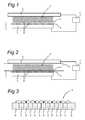
- a cross sectional view of the configuration of a first embodiment of the present inventionis shown in Fig. 1 .
- Two electrodes 2, 3are provided, forming a treatment space 5 in between.
- the electrodes 2, 3are planar electrodes, and the treatment space 5 is a rectangular space.
- other forms of the electrodes 2, 3 and of the treatment space 5are possible, e.g. as part of a cylindrical arrangement of the plasma treatment apparatus.
- a substrate 1 to be treatedmay be positioned in a fixed way or moving at a certain speed in the treatment space 5 close to one of the electrodes 2, 3.
- a mask device 7is used on top of the surface of substrate 1, which in its turn is positioned on top of a magnetic layer 6, which interacts with the mask device 7.
- the mask device 7may be made of conductive material, e.g. a metal mask device 7.
- a metal mask device 7To secure intimate contact between mask device 7 and the surface of substrate 1 the mask device 7 having a predetermined magnetic permeability can be held in close contact with the substrate 1 using the magnetic layer 6. For the best results, there is basically no space between the mask device 7 and the substrate 1, and if there would be a space at all, the distance between mask device 7 and substrate 1 should be e.g. less than 1 micrometer.
- the material to be treated(substrate 1) is sandwiched between the mask device 7 and magnetic layer 6. This solution has the advantage that the bulk plasma generated in treatment space 5 is not obstructed. Main advantages are that the bulk plasma ignites at normal low breakdown voltages and the gas supply to the holes in the mask device 7 towards the surface of the substrate 1 is by diffusion from the bulk plasma.
- the magnetic layer 6is positioned on the bottom (or first) electrode 2, e.g. in the form of a magnetic layer 6.
- the magnetic layer 6is arranged as part of the bottom electrode 2.
- the mask device 7is made of a thin material, in which a pattern is provided as holes or openings 10 in the material for patterning the surface of the substrate 1. As a result, the substrate 1 is sandwiched between the mask device 7 and the magnetic layer 6.
- the magnetic layer 6e.g. comprises small line shaped alternating north and south poles as shown in the cross sectional view of Fig. 3 which have good interaction with the mask device 7.
- the magnetic layer 6can either be conductive or non-conductive.
- a magnetic layer 6was used obtainable from Bakker Magnetics, available under the name 'Natural Magnetic foil', which comprises a semi-anisotropic magnetic layer.
- This flexible foilcomprises alternating magnetic poles at a predefined pitch distance (see e.g. the embodiment shown in Fig. 3 ) Also other flexible magnetic layers from other suppliers may be used.
- the magnetic layere.g. comprises randomly oriented alternating magnetic poles.
- the thickness of the foil usedis as low as possible in order not to interfere with the generation of the glow discharge plasma in the treatment space 5.
- the thickness of the magnetic layer 6is e.g. less than 1 mm, e.g. 0.75 or 0.5 mm In another embodiment also foils may be used with a thickness of more than 1 mm, for example 1.5 or 2 mm or even more.
- the magnetic layers 6 suitable for use in this inventionhave as a fundamental property, that the magnetic field extends through the substrate 1 into the mask device 7 to allow a sufficiently strong attraction force. In order to have this sufficient attractive force the magnetic force should be evenly distributed over the surface of the magnetic layer 6 and exerts a magnetic force of between 5 and 100 g/cm 2 , e.g. 19 or 41 g/cm 2 . A higher magnetic force will allow to use a thinner mask device 7 (less material to attract).
- the mask device 7is made of a material which may have a magnetic permeability of at least 1 Tm/A, e.g. equal to or larger than 5 Tm/A. Very good results are obtained with the mask device having a magnetic permeability of 100, or 500 or 1000 Tm/A or any value in between. Material having such magnetic permeability can be selected from ferromagnetic material, or martensitic or austenitic material having ferromagnetic properties. It is furthermore known, that the attraction between a magnetic material and a material attractive for magnetic force is dependant on the thickness of an intermediate layer (i.e. the substrate 1) and the mask device 7.
- the thickness of the mask device 7is chosen as small as possible in order to have a good interaction with the magnetic layer 6 and as little as possible interference with the generation of the plasma in the treatment space 5.
- the thickness of the mask device 7is less than 1 mm, e.g. less than 0.4 mm, e.g. 0.1 or 0.05 mm.
- Fig. 2a cross sectional view is shown of a plasma treatment apparatus according to a further embodiment of the present invention.
- the DBD structure of the apparatus according to Fig. 1is enhanced by using a further dielectric barrier 4 on the surface of the top (second) electrode 3 directed at the treatment space 5. This will enhance the generation of a stable plasma in the treatment space 5 and may help in providing a stable and uniform glow discharge plasma in case this is needed..
- a glow discharge plasmamay be used advantageously the formation of a glow discharge plasma may be stimulated by controlling the displacement current using a plasma control unit 11 connected to the electrodes 2, 3 (see Fig. 1 and 2 ), and by controlling the distance between electrodes 2, 3, the glow discharge plasma formation can be promoted even into the small holes 10 in the mask device 7, leading to a uniform activation of the (unmasked) surface of substrate 1.
- the plasma control unit 11e.g. comprises a power supply and associated control circuitry as described in the international patent application WO 2007/024134 , and European patent applications EP-A-1381257 , EP-A-1626613 of applicant .
- the mask device 7can be either on a floating potential, be grounded, or be on the same potential as the first (bottom) electrode 2. Depending on the type of material used for the mask device 7 and the substrate 1, and the type of application, these alternatives may provide an optimum result.
- a treatment of a substrate surfaceis provided on the second (or top) electrode 3.
- two surfaces 1can be treated in the vicinity of both electrodes 2, 3.
- the set-up and embodiments applicable for the first electrode 2can also be applied to the second electrode 3 (i.e. sandwich structure of magnetic layer 6, substrate 1 and mask device 7).
- a mechanismmay be provided capable of moving the substrate 1 through the treatment space 5, in order to expose a complete substrate surface.
- the magnetic layer 6is in size at least 90% of the total circumference area of the mask device 7, e.g. 100% or more, and the complete package of magnetic layer 6 and mask device7, with the substrate 1 in between is moved trough the treatment space 5.
- the present method and apparatusmay be used for a localized activation of a hydrophobic substrate 1.
- a thin film of poly-ethylene (PE)is placed in the treatment space 5 of the apparatus of Fig. 1 .
- An argon/nitrogen (5:1) mixture (first example) or an argon/oxygen mixture (5:0.1) (second example)is introduced in the treatment space 5, and a short plasma treatment of 10 seconds was applied (frequency 130 kHz, duty cycle 2% (i.e. the ratio between plasma on time and plasma off time), pulse on-time of 100 ⁇ sec).
- a glow discharge plasmais generated which result in a uniform activation of the (unmasked) surface parts.
- mainly amine/amide-like groupsare formed on the surface of the substrate 1, and in the second case mainly peroxy-,hydroxy- and carboxy- groups are formed.
- the surface of the PE substrate 1becomes hydrophilically patterned, which for example allows easy printing.
- Three different masks(length 90 mm * width 80 mm/0.10 mm thick/AISI 301 material) were produced having different pitch distance (the pitch distance being defined as the distance from the centre point of each square to its direct neighbour square centre point.
- One maskhas a 24 by 24 array of open squares enabling plasma activation with a 0.5 mm square diameter and with a 2.0 mm pitch distance (see top view of embodiment of mask device 7 in Fig. 4 ), the second one having an array of 96 by 24 squares with 0.1 mm square diameter and with 0.2 mm pitch distance and the third mask having having an array of 192 by 192 squares and with a square diameter of 0.02 mm and with 0.04 mm pitch distance. (The last two are not shown here).
- FIG. 5A typical scan across a small part of the plasma patterned substrate 1 is shown in Fig. 5 , showing the energy well formed by plasma patterning using the mask of 0.2 mm pitch distance and 0.1 mm square diameter.
- a Krüss micro contact angle measurement apparatuswas used generating 10 p1 droplet size. It is clear from Fig.5 that it is possible to realize patterns with predefined structures of hydrophobic/hydrophilic areas (or vice versa) and sharp transitions between hydrophilic and hydrophobic area (or vice versa) on substrates 1 by this invention which may be very useful in applications such as micro titer plates manufacturing, electrically conductive paths manufacturing and even transparent conductive patterns manufacturing on substrates 1.
- x 2 and x 1represent the position of the droplets deposited at the border of the surface energy well. Difficulty is that the droplet cannot be deposited on the corner because the droplet will then move in to the surface energy well.
- the inventioncan be used in the application of inkjet printing.
- the inkjet printing nozzlemay have a less accurate output
- the method according to the present inventionallows to control the hydrophobic/hydrophilic surface parts very accurately in a lateral scale.
- the liquid ink dispensed by the nozzlewill automatically move to the area of highest surface energy. This so-called self-alignment (the movement of ink to move to the area of highest surface energy) is clearly visible in the picture shown in Fig.6 .
- the mask with a pitch distance of 0.2 mm and 0.1mm square diameterwas used on a PE-substrate 1 during the plasma patterning while after this treatment the patterned substrate 1 was printed with a 1 p1 print head using a solid print pattern file and a standard black water-based ink by a DMP2831 printer from Fujifilm Dimatix. It is clear that in the plasma patterned area sharp defined structures are visible due to its precise plasma activation resulting in energy wells and as a result of self-alignment of the ink into the activated area while on the edge of the mask (which is non-treated by plasma) coagulation of hydrophilic ink-droplets occurs causing a blurry image because of absence of activated area.
- Materials which also may be used to coat the substrate 1are commercially available conductive inks containing for example silver-particles. Also, gel-based inks based on transparent conductive material can be used. The sol-gel will adhere only to those areas of the substrate 1 which are hydrophilic. Subsequently, the transparent conductive sol gel can be cured by a temperature step or by UV curing. In this manner, a patterned transparent layout can be printed on a polymer surface, which may be used for display applications, or photovoltaic cells.
- etching of a substrate 1 of polymeric base materialmay also be executed using the present method and apparatus embodiments.
- the substrate 1is a PE film.
- Two different gas mixtureswere used, i.e. an argon/oxygen (5:1) mixture and a argon/CF 4 (5:0.1) mixture.
- Plasma treatmentwas carried out in a similar manner as in example 1, applying a total etching time of 60 seconds. After plasma exposure, the depth of trenches and wells in the substrate 1 was determined using a laser profilometer.
- the etch ratewas determined to be 500nm/min, and in the case of the argon/CF 4 mixture, the etch rate was 1 ⁇ m/min.
- the present inventionmay also be used to etch a pattern on the surface of the substrate 1, e.g. by using a gas mixture of Ar, CF 4 and N 2 in the treatment space 5. Areas on the substrate surface exposed to the plasma can be etched in order to generate small holes or channels in e.g. a polymeric material. In case of etching filamentation of the plasma is of no problem. In this case also filamentary plasma's may be used.
- An ITO glass substrate 1(0.7mm thick) was spin coated with a hydrophobic photo resist of 1 ⁇ m thick. Again, argon/oxygen and argon/CF 4 mixtures were used to locally etch the photo resist layer. After two minutes of treatment time, the local water contact angle was determined. It was observed that the surface energy of the areas of the substrate 1 which were not covered by the mask device 7 have an extremely high surface energy of 70 mJ/m 2 , indicating a complete removal of the photo resist. The surface energy of masked areas of the substrate 1 remained very low (typically 30 mJ/m 2 ). This type of processing may be advantageously applied in the manufacturing of organic light emitting devices (OLED).
- OLEDorganic light emitting devices
- the present method an apparatus embodimentsmay also be advantageously applied in deposition of material on a substrate, e.g. inorganic or organic layers, by localized chemical vapour deposition (CVD).
- CVDchemical vapour deposition
- a substratee.g. inorganic or organic layers
- CVDchemical vapour deposition
- a dielectric substrate 1for instance a polymer
- the dimensions of the structure obtainableare ideal for display applications.
- photovoltaic cell contactscan be realized in this way.
- the etching and deposition examplesmay be combined, e.g. to first etch the substrate 1 to form a well or trench and subsequently (possibly using another mask device 7) to locally deposit a coating in the well or trench.
- filamentation of the plasmais not wanted and therefore atmospheric glow discharge plasma's are preferred in this application.
- a surprising applicationis the deposition of a hydrophobic substance to a hydrophilic surface. For example by using an Ar/C2F6 plasma, hydrophobic patterns can be provided an a hydrophilic surface.
Landscapes
- Physics & Mathematics (AREA)
- Engineering & Computer Science (AREA)
- Plasma & Fusion (AREA)
- Chemical & Material Sciences (AREA)
- Analytical Chemistry (AREA)
- Plasma Technology (AREA)
- Chemical Vapour Deposition (AREA)
- Drying Of Semiconductors (AREA)
Description
- The present invention relates to a method for treatment of a substrate surface using atmospheric pressure plasma, the method comprising providing a dielectric barrier discharge electrode structure for generating an atmospheric pressure plasma in a treatment space between a first electrode and a second electrode. In a further aspect, the present invention relates to a plasma treatment apparatus for treatment of a surface of a substrate, comprising a dielectric barrier discharge electrode structure having a treatment space and comprising a first electrode and a second electrode, and a power supply connected to the first electrode and the second electrode for generating an atmospheric pressure plasma in the treatment space.
- European patent application
EP-A-I 750 294 Fig. 4 ), a magnetic field creating means 90 is provided, which functions in shaping the plasma field. - Japanese patent publication
JP-01-033932 - Photo-lithographic patterning is a common technique in semi conductor industry. Plasma etching can be applied to form patterns or structures on an object (for instance a wafer). The patterning technique consists of several time consuming steps: first (spin) coating of a photo resist, second irradiating the photo resist locally by using a mask device, third removing the exposed or non exposed photo resist (depending on the type of resist being positive or negative) and fourth the selective plasma etching treatment. An example of such a technique is given in European
patent application EP 0 889 506 A2 . This document discloses the use of a low pressure RF plasma discharge to pattern (etch) an object placed on one of the electrodes using a photolithogaphic patterning step. - Atmospheric pressure discharges have also been used to create patterns on a substrate, see e.g. international patent application
WO 01/69644 WO 2005/033189 discloses plasma treating of substrates by dielectric barrier discharge masking certain areas of the substrate.- Another solution to pattern a substrate is to make use of a solid re-usable mask device, see e.g. the US patent publication
US 2006/0166111 . In this patent publication a mask device is created by etching holes entirely through a silicon wafer. The silicon wafer is then glued on top of a glass plate to give increased strength. Then the mask device is placed on an object which is irradiated by a laser to etch parts of the irradiated substrate. - The present invention seeks to provide a plasma treatment method and apparatus and the use of the method and apparatus for treatment of the surface of a substrate using a plasma, which allows to provide a pattern on the substrate surface.
- According to the present invention, a method according to the preamble defined above is provided, in which the method further comprises providing a magnetic layer on a surface of at least the first electrode in the treatment space, providing a substrate in contact with the magnetic layer, providing a mask device in contact with the substrate, the mask device interacting with the magnetic layer, and applying a plasma generating power to the first and second electrode for treatment of surface areas of the substrate exposed by the mask device (i.e. exposure of areas not covered by the mask device to the plasma in operation). The interaction between mask device and magnetic layer provides a close or intimate contact between the mask device and the substrate, i.e. there is basically no distance between the mask device and the substrate and if there would be a distance at all, the maximum distance between the mask device and the substrate is less than a predetermined distance, e.g. less than 1 micrometer, in order to prevent any air gaps. Without the application of a magnetic layer there might be a distance between the mask device and the substrate, as a result of which no accurate pattern will be taken over from the mask device on the substrate because of edge effects. The contact is furthermore plan-parallel, i.e. the maximum distance is achieved at any place over the entire substrate surface. In another embodiment the same provisions(mask device, substrate, magnetic layer foil) as applied on the first electrode are also applied to the second electrode. None of the prior art publications described above disclose the use of a mask device positioned on one of the electrodes of an atmospheric DBD system to pattern the substrate covered by the mask device. The present method allows to generate a bulk plasma in the treatment space at normal (low) breakdown voltages without any (structural) obstructions in the treatment space. The supply of reactive gasses (plasma) to the holes and gaps in the masking device near to the surface of the substrate is obtained by diffusion from the bulk plasma. The present method may also be applied to use the second electrode for treatment of a substrate, in which the second electrode is also provided with a magnetic layer, substrate and mask device.
- The electrodes may be planar electrodes, which results in a rectangular treatment space, which allows easy and efficient treatment of flat surfaces of a substrate. The magnetic layer, substrate and mask device form a dielectric barrier on the first electrode, as a result of which the plasma discharge generated may be a very uniform plasma. In a further embodiment the plasma generated may be an atmospheric glow discharge plasma. Possibly, also the second electrode may be provided with a dielectric barrier, allowing to easier generate a uniform atmospheric pressure discharge plasma or glow discharge plasma in the treatment space.
- The mask device may be made of a conductive or non-conductive material, e.g. a metallic or dielectric material, provided the material is able to interact with the magnetic layer. In a further embodiment, the material of the mask device is made from a material which has a magnetic permeability of at least 1 Tm/A, e.g. equal to or larger than 5 Tm/A. Very good results are obtained with the mask device having a magnetic permeability of 100, or 500 or 1000 Tm/A or any value in between. Material having such magnetic permeability can be selected from ferromagnetic material, or martensitic or austenitic material having ferromagnetic properties. This allows a positive attraction force between the mask device and the magnetic layer.
- The thickness of the mask device may in an embodiment be less than 1 mm, e.g. less than 0.4 mm. The thickness may even be as low as 0.1 mm or even 0.05 mm. As a result the dielectric barrier is as small as possible and does not prevent a proper operation of the glow discharge plasma generation.
- Also, the magnetic layer has a thickness which is in a
further embodiment 1 mm or less than 1 mm, e.g. less than 0.5 mm. Again this allows to provide a proper dimension and characteristic of the dielectric barrier on the first electrode. In a further embodiment the thickness of the magnetic layer can be more than 1mm e.g. 1.5 or 2 mm or even thicker. The magnetic layer may comprise alternating magnetic poles at a predefined pitch distance, in which the pitch distance is chosen such that the magnetic field extends through the substrate into the mask device to allow a sufficiently strong attraction force. In another embodiment the magnetic layer may comprise randomly oriented alternating magnetic poles with the condition, that the magnetic field extends through the substrate into the mask device to allow a sufficiently strong attraction force In a further embodiment, the magnetic layer has a magnetic force between 5 g/cm2 and 100 g/cm2, to effectively attract the mask device to the magnetic layer with the substrate in between. - In a further embodiment, the mask device is on a floating potential, grounded, or at first electrode potential. Depending on the type of material of the mask device and the substrate, one of the choices may provide for an optimum result.
- Applying a plasma generating power to the electrodes comprises, in a further embodiment, controlling a displacement current to the first and second electrode. By using feedback control and further stabilization control, a uniform and efficient glow discharge plasma may be formed, in which filamentation of the dielectric barrier discharge plasma may be effectively suppressed. Filamentation would result in localized high density plasma, which may be disadvantageous in certain uses as it may result in dust formation in chemical vapor deposition applications of the present method embodiments. In other applications filamentation is less of a problem, and in such applications stabilization means are of less importance.
- In a further aspect, the present invention relates to a plasma treatment apparatus as defined in the preamble above, the plasma treatment apparatus further comprising a magnetic layer provided on a surface of at least the first electrode (e.g. on top of the surface of the first electrode or as part of the first electrode), and a mask device, the first electrode being arranged to receive, in operation, the substrate to be treated and the mask device in contact with the substrate, the mask device interacting with the magnetic layer. The present apparatus allows to generate a bulk plasma in the treatment space at normal (low) breakdown voltages without any (structural) obstructions in the treatment space. The supply of reactive gasses (plasma) to the holes and gaps in the masking device near to the surface of the substrate is obtained by diffusion from the bulk plasma. The second electrode may also be provided with the magnetic layer, substrate and mask device in operation, allowing simultaneous treatment of two substrates.
- The plasma treatment apparatus may further be arranged to comprise structural features enabling the method embodiments of the present invention. Furthermore, the present invention also relates to a plasma treatment apparatus according to any of the present apparatus embodiments, in which the mask device is made of a material which may have a magnetic permeability of at least 1 Tm/A, e.g. equal to or larger than 5 Tm/A. Very good results are obtained with the mask device having a magnetic permeability of 100, or 500 or 1000 Tm/A or any value in between. Material having such magnetic permeability can be selected from ferromagnetic material, or martensitic or austenitic material having ferromagnetic properties, resulting in a positive attraction between the magnetic layer and the mask device, with the substrate in between.
- In further aspects, the present method or apparatus can be used for providing (or activating) a surface of a substrate with a predefined pattern, e.g. a pattern having sharp transitions (such as a transition of less than 10 µm, even less than 2 µm, or even less than 0.2 µm ). Also, the present method or apparatus can be used for providing a hydrophobic substrate with a predefined hydrophilic pattern (or a hydrophilic substrate with a hydrophobic pattern), for etching a surface of a substrate with a predefined pattern, and for depositing material in a predefined pattern on a surface of a substrate. The pattern can similarly have sharp transitions. The latter use (depositing material on a substrate) can be advantageously applied in printing applications for application of inks on a substrates with a predefined pattern. In an embodiment, a treated substrate is printed on using a material selected from the group consisting of: water based ink, conductive ink, gel based ink. In an embodiment, the use can be applied for providing sharp defined transitions between hydrophic and hydrophilic areas of the substrate, in which the transition length is less than 10 microns, e.g. less than 2 micron or even 0.2 micron.
- The present invention will be discussed in more detail below, using a number of exemplary embodiments, with reference to the attached drawings, in which
Fig. 1 shows a cross sectional view of a first embodiment of a plasma treatment apparatus according to a first embodiment of the present invention;Fig. 2 shows a cross sectional view of a second embodiment of a plasma treatment apparatus according to the present invention;Fig. 3 shows a cross sectional view of an example of a magnetic layer used in the plasma treatment apparatus ofFig. 1 or Fig. 2 ;Fig. 4 shows a top view of a typical mask device with defined structures;Fig. 5 shows a graph representing a typical result of a water contact angle measurement on a plasma patterned substrate;Fig. 6 shows a picture of a typical result after inkjet printing a plasma patterned substrate.- In embodiments of the present invention a standard dielectric barrier discharge (DBD) geometry is used in which atmospheric pressure plasma is generated. A cross sectional view of the configuration of a first embodiment of the present invention is shown in
Fig. 1 . Twoelectrodes treatment space 5 in between. In the embodiment shown, theelectrodes treatment space 5 is a rectangular space. However, other forms of theelectrodes treatment space 5 are possible, e.g. as part of a cylindrical arrangement of the plasma treatment apparatus. - A
substrate 1 to be treated may be positioned in a fixed way or moving at a certain speed in thetreatment space 5 close to one of theelectrodes mask device 7 is used on top of the surface ofsubstrate 1, which in its turn is positioned on top of amagnetic layer 6, which interacts with themask device 7. - The
mask device 7 may be made of conductive material, e.g. ametal mask device 7. To secure intimate contact betweenmask device 7 and the surface ofsubstrate 1 themask device 7 having a predetermined magnetic permeability can be held in close contact with thesubstrate 1 using themagnetic layer 6. For the best results, there is basically no space between themask device 7 and thesubstrate 1, and if there would be a space at all, the distance betweenmask device 7 andsubstrate 1 should be e.g. less than 1 micrometer. The material to be treated (substrate 1) is sandwiched between themask device 7 andmagnetic layer 6. This solution has the advantage that the bulk plasma generated intreatment space 5 is not obstructed. Main advantages are that the bulk plasma ignites at normal low breakdown voltages and the gas supply to the holes in themask device 7 towards the surface of thesubstrate 1 is by diffusion from the bulk plasma. - The
magnetic layer 6 is positioned on the bottom (or first)electrode 2, e.g. in the form of amagnetic layer 6. As an alternative, themagnetic layer 6 is arranged as part of thebottom electrode 2. Themask device 7 is made of a thin material, in which a pattern is provided as holes oropenings 10 in the material for patterning the surface of thesubstrate 1. As a result, thesubstrate 1 is sandwiched between themask device 7 and themagnetic layer 6. - In one embodiment, the
magnetic layer 6 e.g. comprises small line shaped alternating north and south poles as shown in the cross sectional view ofFig. 3 which have good interaction with themask device 7. Themagnetic layer 6 can either be conductive or non-conductive. In an example, amagnetic layer 6 was used obtainable from Bakker Magnetics, available under the name 'Natural Magnetic foil', which comprises a semi-anisotropic magnetic layer. This flexible foil comprises alternating magnetic poles at a predefined pitch distance (see e.g. the embodiment shown inFig. 3 ) Also other flexible magnetic layers from other suppliers may be used. In anothermagnetic layer 6 which may be used, the magnetic layer e.g. comprises randomly oriented alternating magnetic poles. The thickness of the foil used is as low as possible in order not to interfere with the generation of the glow discharge plasma in thetreatment space 5. The thickness of themagnetic layer 6 is e.g. less than 1 mm, e.g. 0.75 or 0.5 mm In another embodiment also foils may be used with a thickness of more than 1 mm, for example 1.5 or 2 mm or even more. Themagnetic layers 6 suitable for use in this invention have as a fundamental property, that the magnetic field extends through thesubstrate 1 into themask device 7 to allow a sufficiently strong attraction force. In order to have this sufficient attractive force the magnetic force should be evenly distributed over the surface of themagnetic layer 6 and exerts a magnetic force of between 5 and 100 g/cm2, e.g. 19 or 41 g/cm2. A higher magnetic force will allow to use a thinner mask device 7 (less material to attract). - The
mask device 7 is made of a material which may have a magnetic permeability of at least 1 Tm/A, e.g. equal to or larger than 5 Tm/A. Very good results are obtained with the mask device having a magnetic permeability of 100, or 500 or 1000 Tm/A or any value in between. Material having such magnetic permeability can be selected from ferromagnetic material, or martensitic or austenitic material having ferromagnetic properties. It is furthermore known, that the attraction between a magnetic material and a material attractive for magnetic force is dependant on the thickness of an intermediate layer (i.e. the substrate 1) and themask device 7. In further embodiments, the thickness of themask device 7 is chosen as small as possible in order to have a good interaction with themagnetic layer 6 and as little as possible interference with the generation of the plasma in thetreatment space 5. For this, the thickness of themask device 7 is less than 1 mm, e.g. less than 0.4 mm, e.g. 0.1 or 0.05 mm. - In
Fig. 2 a cross sectional view is shown of a plasma treatment apparatus according to a further embodiment of the present invention. The DBD structure of the apparatus according toFig. 1 is enhanced by using a furtherdielectric barrier 4 on the surface of the top (second)electrode 3 directed at thetreatment space 5. This will enhance the generation of a stable plasma in thetreatment space 5 and may help in providing a stable and uniform glow discharge plasma in case this is needed.. - In an embodiment where a glow discharge plasma may be used advantageously the formation of a glow discharge plasma may be stimulated by controlling the displacement current using a
plasma control unit 11 connected to theelectrodes 2, 3 (seeFig. 1 and 2 ), and by controlling the distance betweenelectrodes small holes 10 in themask device 7, leading to a uniform activation of the (unmasked) surface ofsubstrate 1. Theplasma control unit 11 e.g. comprises a power supply and associated control circuitry as described in the international patent applicationWO 2007/024134 , and European patent applicationsEP-A-1381257 ,EP-A-1626613 of applicant . Themask device 7 can be either on a floating potential, be grounded, or be on the same potential as the first (bottom)electrode 2. Depending on the type of material used for themask device 7 and thesubstrate 1, and the type of application, these alternatives may provide an optimum result. - In a further embodiment of this invention also a treatment of a substrate surface is provided on the second (or top)
electrode 3. In this embodiment at the same time twosurfaces 1 can be treated in the vicinity of bothelectrodes first electrode 2 can also be applied to the second electrode 3 (i.e. sandwich structure ofmagnetic layer 6,substrate 1 and mask device 7). - As the
plasma generating electrodes substrate 1 through thetreatment space 5, in order to expose a complete substrate surface. In the embodiment with a movingsubstrate 1 in one exemplary embodiment themagnetic layer 6 is in size at least 90% of the total circumference area of themask device 7, e.g. 100% or more, and the complete package ofmagnetic layer 6 and mask device7, with thesubstrate 1 in between is moved trough thetreatment space 5. - The present method and apparatus may be used for a localized activation of a
hydrophobic substrate 1. A thin film of poly-ethylene (PE), is placed in thetreatment space 5 of the apparatus ofFig. 1 . An argon/nitrogen (5:1) mixture (first example) or an argon/oxygen mixture (5:0.1) (second example) is introduced in thetreatment space 5, and a short plasma treatment of 10 seconds was applied (frequency 130 kHz,duty cycle 2% (i.e. the ratio between plasma on time and plasma off time), pulse on-time of 100 µsec). By controlling the displacement current and electrode distance, a glow discharge plasma is generated which result in a uniform activation of the (unmasked) surface parts. In the first case, mainly amine/amide-like groups are formed on the surface of thesubstrate 1, and in the second case mainly peroxy-,hydroxy- and carboxy- groups are formed. In both cases, the surface of thePE substrate 1 becomes hydrophilically patterned, which for example allows easy printing. - Some examples of the possible surface modifications are shown in the table below.
Gas mixtures Chemical bonds formed Ar + N2 =NH, -NH2 N2 + NH3 -NH2 Ar +O2 -OH, C=O N2 + CO2 -COOH - Different masks were used to pattern the hydrophobic polymer surface of the
PE substrate 1. - Three different masks (length 90 mm *
width 80 mm/0.10 mm thick/AISI 301 material) were produced having different pitch distance (the pitch distance being defined as the distance from the centre point of each square to its direct neighbour square centre point. One mask has a 24 by 24 array of open squares enabling plasma activation with a 0.5 mm square diameter and with a 2.0 mm pitch distance (see top view of embodiment ofmask device 7 inFig. 4 ), the second one having an array of 96 by 24 squares with 0.1 mm square diameter and with 0.2 mm pitch distance and the third mask having having an array of 192 by 192 squares and with a square diameter of 0.02 mm and with 0.04 mm pitch distance. (The last two are not shown here). - A typical scan across a small part of the plasma patterned
substrate 1 is shown inFig. 5 , showing the energy well formed by plasma patterning using the mask of 0.2 mm pitch distance and 0.1 mm square diameter. A Krüss micro contact angle measurement apparatus was used generating 10 p1 droplet size. It is clear fromFig.5 that it is possible to realize patterns with predefined structures of hydrophobic/hydrophilic areas (or vice versa) and sharp transitions between hydrophilic and hydrophobic area (or vice versa) onsubstrates 1 by this invention which may be very useful in applications such as micro titer plates manufacturing, electrically conductive paths manufacturing and even transparent conductive patterns manufacturing onsubstrates 1. - In order to quantitatively describe the sharp transition from hydrophilic to hydrophobic or vice versa we have defined a parameter which characterises how sudden the wettability transition η "happens".

- Where x2 and x1 represent the position of the droplets deposited at the border of the surface energy well. Difficulty is that the droplet cannot be deposited on the corner because the droplet will then move in to the surface energy well.
- From the graph of
substrate 1 inFig 5 an η = 8 °/µm can be derived, which indicates that sharp transitions between the hydrophilic to hydrophobic area (or vice versa) can be achieved smaller than 10 micron. To obtain even more detailed information about the typical sharpness of the wettability transition more detailed analysis measurements were carried out with the micro contact angle equipment using 1 and 5 p1 droplets taking intervals as small as 1 µm. Based on these measurements an η= 50 °/µm is observed, which indicates the transition between the hydrophilic to hydrophobic area (or vice versa) are very sharp and even smaller than 2 micron e.g. even 0.2 micron. - Advantageously, the invention can be used in the application of inkjet printing. Although the inkjet printing nozzle may have a less accurate output, the method according to the present invention allows to control the hydrophobic/hydrophilic surface parts very accurately in a lateral scale. The liquid ink dispensed by the nozzle will automatically move to the area of highest surface energy. This so-called self-alignment (the movement of ink to move to the area of highest surface energy) is clearly visible in the picture shown in
Fig.6 . In this particular example the mask with a pitch distance of 0.2 mm and 0.1mm square diameter was used on a PE-substrate 1 during the plasma patterning while after this treatment the patternedsubstrate 1 was printed with a 1 p1 print head using a solid print pattern file and a standard black water-based ink by a DMP2831 printer from Fujifilm Dimatix. It is clear that in the plasma patterned area sharp defined structures are visible due to its precise plasma activation resulting in energy wells and as a result of self-alignment of the ink into the activated area while on the edge of the mask (which is non-treated by plasma) coagulation of hydrophilic ink-droplets occurs causing a blurry image because of absence of activated area. - Materials which also may be used to coat the
substrate 1 are commercially available conductive inks containing for example silver-particles. Also, gel-based inks based on transparent conductive material can be used. The sol-gel will adhere only to those areas of thesubstrate 1 which are hydrophilic. Subsequently, the transparent conductive sol gel can be cured by a temperature step or by UV curing. In this manner, a patterned transparent layout can be printed on a polymer surface, which may be used for display applications, or photovoltaic cells. - It may be further clear from the shown example that the method and apparatus according to the present invention may be useful in the application of other printing techniques such as offset printing.
- Localized etching of a
substrate 1 of polymeric base material (including Si wafer, glass, inorganic coatings, etc.) may also be executed using the present method and apparatus embodiments. In this example, thesubstrate 1 is a PE film. Two different gas mixtures were used, i.e. an argon/oxygen (5:1) mixture and a argon/CF4 (5:0.1) mixture. Plasma treatment was carried out in a similar manner as in example 1, applying a total etching time of 60 seconds. After plasma exposure, the depth of trenches and wells in thesubstrate 1 was determined using a laser profilometer. In the case of argon/oxygen mixture, the etch rate was determined to be 500nm/min, and in the case of the argon/CF4 mixture, the etch rate was 1 µm/min. The present invention may also be used to etch a pattern on the surface of thesubstrate 1, e.g. by using a gas mixture of Ar, CF4 and N2 in thetreatment space 5. Areas on the substrate surface exposed to the plasma can be etched in order to generate small holes or channels in e.g. a polymeric material. In case of etching filamentation of the plasma is of no problem. In this case also filamentary plasma's may be used. - An ITO glass substrate 1 (0.7mm thick) was spin coated with a hydrophobic photo resist of 1 µm thick. Again, argon/oxygen and argon/CF4 mixtures were used to locally etch the photo resist layer. After two minutes of treatment time, the local water contact angle was determined. It was observed that the surface energy of the areas of the
substrate 1 which were not covered by themask device 7 have an extremely high surface energy of 70 mJ/m2, indicating a complete removal of the photo resist. The surface energy of masked areas of thesubstrate 1 remained very low (typically 30 mJ/m2). This type of processing may be advantageously applied in the manufacturing of organic light emitting devices (OLED). - The present method an apparatus embodiments may also be advantageously applied in deposition of material on a substrate, e.g. inorganic or organic layers, by localized chemical vapour deposition (CVD). E.g. small patterns of silicon oxide were produced. Even transparent conductive coatings can be produced so that a patterned electrically conductive path can be deposited on a dielectric substrate 1 (for instance a polymer). The dimensions of the structure obtainable are ideal for display applications. Furthermore, photovoltaic cell contacts can be realized in this way. Furthermore, the etching and deposition examples may be combined, e.g. to first etch the
substrate 1 to form a well or trench and subsequently (possibly using another mask device 7) to locally deposit a coating in the well or trench. In the case of a deposition application filamentation of the plasma is not wanted and therefore atmospheric glow discharge plasma's are preferred in this application. - Other applications of the plasma treatment apparatus and method of the present invention include, but are not limited to, patterning applications as applied in Flex Circuits, RFID , PCB Photomasks, Wearable Electronics, Solar, Fuel Cells, Batteries, Flat Panel Displays, PLED, LCD, Color Filters, Display Backplanes, Flexible Displays, Microtiter plates for DNA, Proteomics, Antibodies identification Food Science, Pathogen Detection, medical devices, coatings, optical lenses, light pipes, etc. A surprising application is the deposition of a hydrophobic substance to a hydrophilic surface. For example by using an Ar/C2F6 plasma, hydrophobic patterns can be provided an a hydrophilic surface.

Claims (15)
- Method for treatment of a substrate surface (1) using atmospheric pressure plasma, the method comprising:providing a dielectric barrier discharge electrode structure for generating an atmospheric pressure plasma in a treatment space (5) between a first electrode (2) and a second electrode (3),characterized in that the method further comprises:providing a magnetic layer (6) on a surface of at least the first electrode (2),providing a substrate (1) in contact with the magnetic layer (6),providing a mask device (7) in contact with the substrate (1), the mask device (7) interacting with the magnetic layer (6), andapplying a plasma generating power to the first and second electrode (2, 3) for treatment of surface areas of the substrate (1) exposed by the mask device (7).
- Method according to claim 1, in which the mask device (7) is made of material with a magnetic permeability of at least 1 Tm/A, e.g. equal to or larger than 5 Tm/A.
- Method according to claim 2, in which the thickness of the mask device (7) is less than 1 mm, e.g. less than 0.4 mm.
- Method according to any one of claims 1-3, in which the magnetic layer (6) has a thickness of less than 1 mm, e.g. less than 0.5 mm.
- Method according to claim 4, in which the magnetic layer (6) has a magnetic force between 5 g/cm2 and 100 g/cm2.
- Method according to any one of claims 1-5, in which the mask device (7) is on a floating potential, grounded, or at first electrode potential,
- Method according to any one of claims 1-6, in which the generated plasma is an atmospheric pressure glow discharge plasma or a filamentary atmospheric plasma.
- Method according to any one of claims 1-7, in which applying a plasma generating power comprises controlling a displacement current to the first and second electrode (2, 3).
- Plasma treatment apparatus arranged to treat a surface of a substrate, comprising
a dielectric barrier discharge electrode structure having a treatment space (5) and comprising a first electrode (2) and a second electrode (3), and a power supply (11) connected to the first electrode (2) and the second electrode (3) arranged to generate an atmospheric pressure plasma in the treatment space (5),
characterized in that the plasma treatment apparatus further comprises:- a magnetic layer (6) provided on a surface of at least the first electrode (2), and- a mask device (7),the first electrode (2) being arranged to receive, in operation, the substrate (1) to be treated and the mask device (7) in contact with the substrate (1), the mask device (7) being arranged to interact with the magnetic layer (6). - Plasma treatment apparatus according to claim 9, in which the magnetic layer (6) has a thickness of less than 1 mm, e.g. less than 0.5 mm.
- Plasma treatment apparatus according to claim 9 or 10, in which the magnetic layer (6) has a magnetic force between 5 g/cm2 and 100 g/cm2.
- Plasma treatment apparatus according to claim 9, 10, or 11, in which in operation, the mask device (7) is arranged to be on a floating potential, grounded, or at first electrode potential.
- Plasma treatment apparatus according to any one of claims 9-12, in which the generated plasma is an atmospheric pressure glow discharge plasma or a filamentary atmospheric plasma.
- Plasma treatment apparatus according to any one of claims 9-13, in which the power supply (11) is arranged to control a displacement current to the first and second electrode (2, 3).
- Plasma treatment apparatus according to any one of claims 9-14, in which the mask device (7) has a magnetic permeability of at least 1 Tm/A, e.g. equal to or larger than 5 Tm/A.
Priority Applications (1)
| Application Number | Priority Date | Filing Date | Title |
|---|---|---|---|
| EP20080705123EP2109876B1 (en) | 2007-02-13 | 2008-02-01 | Substrate plasma treatment using magnetic mask device |
Applications Claiming Priority (3)
| Application Number | Priority Date | Filing Date | Title |
|---|---|---|---|
| EP07102269 | 2007-02-13 | ||
| EP20080705123EP2109876B1 (en) | 2007-02-13 | 2008-02-01 | Substrate plasma treatment using magnetic mask device |
| PCT/NL2008/050054WO2008100139A1 (en) | 2007-02-13 | 2008-02-01 | Substrate plasma treatment using magnetic mask device |
Publications (2)
| Publication Number | Publication Date |
|---|---|
| EP2109876A1 EP2109876A1 (en) | 2009-10-21 |
| EP2109876B1true EP2109876B1 (en) | 2015-05-06 |
Family
ID=38169702
Family Applications (1)
| Application Number | Title | Priority Date | Filing Date |
|---|---|---|---|
| EP20080705123Not-in-forceEP2109876B1 (en) | 2007-02-13 | 2008-02-01 | Substrate plasma treatment using magnetic mask device |
Country Status (4)
| Country | Link |
|---|---|
| US (1) | US8338307B2 (en) |
| EP (1) | EP2109876B1 (en) |
| JP (1) | JP5506401B2 (en) |
| WO (1) | WO2008100139A1 (en) |
Families Citing this family (17)
| Publication number | Priority date | Publication date | Assignee | Title |
|---|---|---|---|---|
| KR101303447B1 (en)* | 2009-01-21 | 2013-09-05 | 엘지디스플레이 주식회사 | Evaporation Apparatus For Organic Light Emitting Display |
| EP1917842B1 (en)* | 2005-08-26 | 2015-03-11 | FUJIFILM Manufacturing Europe B.V. | Method and arrangement for generating and controlling a discharge plasma |
| EP2024533A1 (en) | 2006-05-30 | 2009-02-18 | Fuji Film Manufacturing Europe B.V. | Method and apparatus for deposition using pulsed atmospheric pressure glow discharge |
| US20090324971A1 (en)* | 2006-06-16 | 2009-12-31 | Fujifilm Manufacturing Europe B.V. | Method and apparatus for atomic layer deposition using an atmospheric pressure glow discharge plasma |
| JP5597551B2 (en)* | 2008-02-01 | 2014-10-01 | フジフィルム マニュファクチュアリング ヨーロッパ ビー.ヴィ. | Apparatus and method for plasma surface treatment of moving substrate and use of the method |
| EP2241165B1 (en)* | 2008-02-08 | 2011-08-31 | Fujifilm Manufacturing Europe B.V. | Method for manufacturing a multi_layer stack structure with improved wvtr barrier property |
| US8609203B2 (en)* | 2008-06-06 | 2013-12-17 | Fujifilm Manufacturing Europe B.V. | Method and apparatus for plasma surface treatment of moving substrate |
| GB0910040D0 (en)* | 2009-06-11 | 2009-07-22 | Fujifilm Mfg Europe Bv | Substrate structure |
| KR20130000218A (en)* | 2011-06-22 | 2013-01-02 | 삼성디스플레이 주식회사 | Electrode including magnetic material and organic light emitting device using the electrode |
| TW201507735A (en) | 2013-08-16 | 2015-03-01 | Ind Tech Res Inst | Plasma generator, surface treatment method using the same and surface treatment method using the same for bio-tissue |
| CN104436956A (en)* | 2014-11-17 | 2015-03-25 | 安吉润风空气净化科技有限公司 | Dielectric-barrier discharging gas purification device |
| JP2016161861A (en)* | 2015-03-04 | 2016-09-05 | 株式会社東芝 | Illumination apparatus |
| KR101741236B1 (en)* | 2016-08-25 | 2017-05-29 | 김동민 | Method of performing preprocessing and printing on flexible substrate and system therefor |
| JP7232571B2 (en)* | 2017-05-31 | 2023-03-03 | シシド静電気株式会社 | Discharge treatment device for skin surface |
| CN116209578A (en)* | 2020-05-15 | 2023-06-02 | 莫塞尔挤出有限责任公司 | Machines for surface treatment of membranes |
| US11584140B2 (en)* | 2020-07-31 | 2023-02-21 | Kyocera Document Solutions Inc. | Concealable marking |
| KR20230089451A (en) | 2021-12-13 | 2023-06-20 | 삼성전자주식회사 | Apparatus for plasma etching, method for plasma etching using the same and method for manufacturing semiconductor device using the same |
Family Cites Families (82)
| Publication number | Priority date | Publication date | Assignee | Title |
|---|---|---|---|---|
| DE3224234A1 (en)* | 1981-09-01 | 1983-03-10 | Siemens AG, 1000 Berlin und 8000 München | METHOD FOR PRODUCING METAL-FREE STRIPS IN THE METAL STEAMING OF AN INSULATING TAPE AND DEVICE FOR IMPLEMENTING THE METHOD |
| JPS58111380A (en) | 1981-12-24 | 1983-07-02 | Seiko Epson Corp | Manufacture of amorphous silicon solar cell |
| JPS58217344A (en) | 1983-06-01 | 1983-12-17 | 旭化成ポリフレックス株式会社 | Barrier plastic laminate sheet |
| US4681780A (en)* | 1983-12-01 | 1987-07-21 | Polaroid Corporation | Continuously cleaned rotary coating mask |
| US4631199A (en)* | 1985-07-22 | 1986-12-23 | Hughes Aircraft Company | Photochemical vapor deposition process for depositing oxide layers |
| JPS6433932A (en) | 1987-07-29 | 1989-02-03 | Matsushita Electric Industrial Co Ltd | Etching apparatus |
| JPH02266524A (en)* | 1989-04-06 | 1990-10-31 | Sankyo Seiki Mfg Co Ltd | Formation of protective coat |
| JPH0494169A (en) | 1990-08-09 | 1992-03-26 | Kanegafuchi Chem Ind Co Ltd | Thin film diode element |
| JP2699695B2 (en)* | 1991-06-07 | 1998-01-19 | 日本電気株式会社 | Chemical vapor deposition |
| US5187457A (en)* | 1991-09-12 | 1993-02-16 | Eni Div. Of Astec America, Inc. | Harmonic and subharmonic filter |
| US5660744A (en)* | 1992-03-26 | 1997-08-26 | Kabushiki Kaisha Toshiba | Plasma generating apparatus and surface processing apparatus |
| JPH06168932A (en)* | 1992-11-30 | 1994-06-14 | Dainippon Printing Co Ltd | Semiconductor device patterning device |
| FR2704558B1 (en)* | 1993-04-29 | 1995-06-23 | Air Liquide | METHOD AND DEVICE FOR CREATING A DEPOSIT OF SILICON OXIDE ON A SOLID TRAVELING SUBSTRATE. |
| JP3148910B2 (en) | 1993-09-01 | 2001-03-26 | 日本真空技術株式会社 | Plasma CVD film forming method |
| DE4438533A1 (en) | 1994-11-02 | 1996-05-09 | Softal Elektronik Gmbh | Corona treatment at atmos. pressure |
| JPH08241886A (en)* | 1995-03-06 | 1996-09-17 | Ii C Giken:Kk | Plasma processing method |
| US5710067A (en)* | 1995-06-07 | 1998-01-20 | Advanced Micro Devices, Inc. | Silicon oxime film |
| JP3061255B2 (en)* | 1995-08-18 | 2000-07-10 | キヤノン販売株式会社 | Film formation method |
| US6342277B1 (en)* | 1996-08-16 | 2002-01-29 | Licensee For Microelectronics: Asm America, Inc. | Sequential chemical vapor deposition |
| JP3885261B2 (en)* | 1996-11-21 | 2007-02-21 | 東レ株式会社 | Substrate support and substrate support method |
| DE19728472A1 (en) | 1997-07-03 | 1999-01-07 | Siemens Ag | Structuring process |
| US6159559A (en)* | 1997-07-07 | 2000-12-12 | The Penn State Research Foundation | Low temperature, high quality silicon dioxide thin films deposited using tetramethylsilane (TMS) |
| AU742051B2 (en) | 1997-07-14 | 2001-12-13 | University Of Tennessee Research Corporation, The | Plasma treater systems and treatment methods |
| US6464421B1 (en)* | 1998-04-02 | 2002-10-15 | Ran Enterprises, Inc. | Jack extension tube for a power seat adjuster mechanism for a vehicle |
| JP2000026632A (en) | 1998-07-13 | 2000-01-25 | Sekisui Chem Co Ltd | Thin film formation on film substrate using normal pressure plasma |
| US6774018B2 (en) | 1999-02-01 | 2004-08-10 | Sigma Laboratories Of Arizona, Inc. | Barrier coatings produced by atmospheric glow discharge |
| EP1029702B1 (en) | 1999-02-15 | 2004-04-14 | Konica Corporation | Surface treatment method, production method for ink jet recording medium, and ink jet recording medium |
| JP2000313962A (en) | 1999-04-26 | 2000-11-14 | Sekisui Chem Co Ltd | DEPOSITION OF TiO2 THIN FILM USING DISCHARGE PLASMA |
| US7091605B2 (en)* | 2001-09-21 | 2006-08-15 | Eastman Kodak Company | Highly moisture-sensitive electronic device element and method for fabrication |
| US6391785B1 (en) | 1999-08-24 | 2002-05-21 | Interuniversitair Microelektronica Centrum (Imec) | Method for bottomless deposition of barrier layers in integrated circuit metallization schemes |
| US6413645B1 (en)* | 2000-04-20 | 2002-07-02 | Battelle Memorial Institute | Ultrabarrier substrates |
| TW520453B (en) | 1999-12-27 | 2003-02-11 | Seiko Epson Corp | A method to fabricate thin insulating films |
| DE10011276A1 (en)* | 2000-03-08 | 2001-09-13 | Wolff Walsrode Ag | Process employing indirect atmospheric plasmatron, surface-treats or coats thin metallic foil or polymer sheet |
| ATE245310T1 (en) | 2000-03-14 | 2003-08-15 | Fraunhofer Ges Forschung | METHOD AND DEVICE FOR PLASMA-ASSISTED SURFACE TREATMENT AND USE OF THE METHOD |
| DE10037957C1 (en)* | 2000-07-27 | 2002-02-28 | Infineon Technologies Ag | Process for the anisotropic dry etching of organic anti-reflection layers |
| US6524431B1 (en)* | 2000-11-10 | 2003-02-25 | Helix Technology Inc. | Apparatus for automatically cleaning mask |
| CA2435852A1 (en) | 2000-11-14 | 2002-05-23 | Sekisui Chemical Co., Ltd. | A method for plasma treatment under the atmospheric pressure and an equipment therefor |
| US6835425B2 (en) | 2000-12-12 | 2004-12-28 | Konica Corporation | Layer-forming method using plasma state reactive gas |
| US6464779B1 (en) | 2001-01-19 | 2002-10-15 | Novellus Systems, Inc. | Copper atomic layer chemical vapor desposition |
| GB0113751D0 (en)* | 2001-06-06 | 2001-07-25 | Dow Corning | Surface treatment |
| US6861334B2 (en)* | 2001-06-21 | 2005-03-01 | Asm International, N.V. | Method of fabricating trench isolation structures for integrated circuits using atomic layer deposition |
| CA2352567A1 (en) | 2001-07-06 | 2003-01-06 | Mohamed Latreche | Translucent material displaying ultra-low transport of gases and vapors, and method for its production |
| US7098131B2 (en)* | 2001-07-19 | 2006-08-29 | Samsung Electronics Co., Ltd. | Methods for forming atomic layers and thin films including tantalum nitride and devices including the same |
| US6756318B2 (en)* | 2001-09-10 | 2004-06-29 | Tegal Corporation | Nanolayer thick film processing system and method |
| JP2003115578A (en)* | 2001-10-05 | 2003-04-18 | Canon Inc | Non-volatile solid-state magnetic memory device, method of manufacturing the same, and multi-chip package |
| DE10161469A1 (en)* | 2001-12-13 | 2003-07-03 | Schott Glas | Volume-optimized reactor for simultaneous coating of spectacle lenses on both sides |
| JP3891267B2 (en)* | 2001-12-25 | 2007-03-14 | キヤノンアネルバ株式会社 | Silicon oxide film manufacturing method |
| JP3859518B2 (en) | 2002-01-15 | 2006-12-20 | 住友ベークライト株式会社 | Transparent water vapor barrier film |
| JP2003249399A (en)* | 2002-02-22 | 2003-09-05 | Sekisui Chem Co Ltd | Discharge plasma processing device |
| EP2249413A3 (en) | 2002-04-01 | 2011-02-02 | Konica Corporation | Support and organic electroluminescence element comprising the support |
| JP4278915B2 (en)* | 2002-04-02 | 2009-06-17 | 東京エレクトロン株式会社 | Etching method |
| US6759100B2 (en) | 2002-06-10 | 2004-07-06 | Konica Corporation | Layer formation method, and substrate with a layer formed by the method |
| JP2004091913A (en)* | 2002-07-10 | 2004-03-25 | Sony Corp | Film deposition system and film deposition method |
| US6774569B2 (en)* | 2002-07-11 | 2004-08-10 | Fuji Photo Film B.V. | Apparatus for producing and sustaining a glow discharge plasma under atmospheric conditions |
| US7288204B2 (en) | 2002-07-19 | 2007-10-30 | Fuji Photo Film B.V. | Method and arrangement for treating a substrate with an atmospheric pressure glow plasma (APG) |
| US20050084610A1 (en)* | 2002-08-13 | 2005-04-21 | Selitser Simon I. | Atmospheric pressure molecular layer CVD |
| EP1403902A1 (en) | 2002-09-30 | 2004-03-31 | Fuji Photo Film B.V. | Method and arrangement for generating an atmospheric pressure glow discharge plasma (APG) |
| JP4303935B2 (en)* | 2002-10-03 | 2009-07-29 | 大日本印刷株式会社 | Manufacturing method of organic EL element |
| CN100450647C (en) | 2003-09-09 | 2009-01-14 | 陶氏环球技术公司 | Glow discharge-generated chemical vapor deposition |
| GB0323295D0 (en)* | 2003-10-04 | 2003-11-05 | Dow Corning | Deposition of thin films |
| US20050079418A1 (en)* | 2003-10-14 | 2005-04-14 | 3M Innovative Properties Company | In-line deposition processes for thin film battery fabrication |
| DE602004024576D1 (en) | 2003-12-22 | 2010-01-21 | Fujifilm Mfg Europe Bv | METHOD AND ARRANGEMENT FOR REMOVING CONTAMINATION FROM A SUBSTRATE SURFACE USING AN ATMOSPHERIC PRESSURE GLASS PLASMA |
| EP1548795A1 (en) | 2003-12-22 | 2005-06-29 | Fuji Photo Film B.V. | Method and apparatus for stabilizing a glow discharge plasma under atmospheric conditions |
| JP2006004740A (en) | 2004-06-17 | 2006-01-05 | Seiko Epson Corp | Film forming method, display device manufacturing method, display device, and electronic apparatus |
| DE602004003697T2 (en) | 2004-08-13 | 2007-10-04 | Fuji Film Manufacturing Europe B.V. | Method and apparatus for controlling a glow discharge plasma at atmospheric pressure |
| DE102004043384B4 (en) | 2004-09-08 | 2010-06-17 | Schott Ag | Process for producing a coated hollow body substrate of at least polyethylene terephthalate |
| JP2006201538A (en)* | 2005-01-21 | 2006-08-03 | Seiko Epson Corp | Mask, mask manufacturing method, pattern forming method, wiring pattern forming method |
| US20060231908A1 (en)* | 2005-04-13 | 2006-10-19 | Xerox Corporation | Multilayer gate dielectric |
| WO2007013703A1 (en) | 2005-07-26 | 2007-02-01 | Psm Inc. | Injection type plasma treatment apparatus and method |
| KR101218114B1 (en) | 2005-08-04 | 2013-01-18 | 주성엔지니어링(주) | Etching apparatus using the plasma |
| EP1917842B1 (en) | 2005-08-26 | 2015-03-11 | FUJIFILM Manufacturing Europe B.V. | Method and arrangement for generating and controlling a discharge plasma |
| US7622393B2 (en)* | 2005-11-04 | 2009-11-24 | Tokyo Electron Limited | Method and apparatus for manufacturing a semiconductor device, control program thereof and computer-readable storage medium storing the control program |
| US7763114B2 (en) | 2005-12-28 | 2010-07-27 | 3M Innovative Properties Company | Rotatable aperture mask assembly and deposition system |
| WO2007089146A1 (en) | 2006-02-02 | 2007-08-09 | Fujifilm Manufacturing Europe B.V. | Method for surface treatment by plasma and surface treatment apparatus |
| WO2007091891A1 (en) | 2006-02-09 | 2007-08-16 | Fujifilm Manufacturing Europe B.V. | Short pulse atmospheric pressure glow discharge method and apparatus |
| EP2024533A1 (en)* | 2006-05-30 | 2009-02-18 | Fuji Film Manufacturing Europe B.V. | Method and apparatus for deposition using pulsed atmospheric pressure glow discharge |
| US20090324971A1 (en)* | 2006-06-16 | 2009-12-31 | Fujifilm Manufacturing Europe B.V. | Method and apparatus for atomic layer deposition using an atmospheric pressure glow discharge plasma |
| JP5597551B2 (en)* | 2008-02-01 | 2014-10-01 | フジフィルム マニュファクチュアリング ヨーロッパ ビー.ヴィ. | Apparatus and method for plasma surface treatment of moving substrate and use of the method |
| EP2241165B1 (en)* | 2008-02-08 | 2011-08-31 | Fujifilm Manufacturing Europe B.V. | Method for manufacturing a multi_layer stack structure with improved wvtr barrier property |
| US20110014424A1 (en)* | 2008-02-21 | 2011-01-20 | Fujifilm Manufacturing Europe B.V. | Plasma treatment apparatus and method for treatment of a substrate with atmospheric pressure glow discharge electrode configuration |
| US8609203B2 (en)* | 2008-06-06 | 2013-12-17 | Fujifilm Manufacturing Europe B.V. | Method and apparatus for plasma surface treatment of moving substrate |
| WO2010092384A1 (en) | 2009-02-12 | 2010-08-19 | Fujifilm Manufacturing Europe Bv | Two layer barrier on polymeric substrate |
- 2008
- 2008-02-01EPEP20080705123patent/EP2109876B1/ennot_activeNot-in-force
- 2008-02-01USUS12/526,944patent/US8338307B2/ennot_activeExpired - Fee Related
- 2008-02-01WOPCT/NL2008/050054patent/WO2008100139A1/enactiveApplication Filing
- 2008-02-01JPJP2009549540Apatent/JP5506401B2/enactiveActive
Also Published As
| Publication number | Publication date |
|---|---|
| EP2109876A1 (en) | 2009-10-21 |
| JP5506401B2 (en) | 2014-05-28 |
| US8338307B2 (en) | 2012-12-25 |
| WO2008100139A1 (en) | 2008-08-21 |
| US20100147794A1 (en) | 2010-06-17 |
| JP2010518586A (en) | 2010-05-27 |
Similar Documents
| Publication | Publication Date | Title |
|---|---|---|
| EP2109876B1 (en) | Substrate plasma treatment using magnetic mask device | |
| EP2235735B1 (en) | Method and apparatus for plasma surface treatment of a moving substrate | |
| EP2537398B1 (en) | Device and method for generating a plasma discharge for patterning the surface of a substrate | |
| US8702902B2 (en) | Device for generating a plasma discharge for patterning the surface of a substrate | |
| EP2200829B1 (en) | Ambient plasma treament of printer components | |
| EP2351872B1 (en) | Treatment method using plasma | |
| KR100753954B1 (en) | Method for forming wiring pattern, method for manufacturing device, and device | |
| TW200817830A (en) | Method for manufacturing mask, method for manufacturing wiring pattern, and method for manufacturing plasma display | |
| US20060183036A1 (en) | Method of forming film pattern, method of manufacturing device, electro-optical device, and electronic apparatus | |
| EP0583997A1 (en) | Topographical selective patterns | |
| US20120288637A1 (en) | Methods of affecting material properties and applications therefor | |
| EP1652590B1 (en) | Method for coating a substrate with a thin film pattern | |
| KR19990023939A (en) | Ink-jet printheads and their manufacturing method | |
| JP4180706B2 (en) | Substance / Material Processing Method | |
| EP1587139A2 (en) | Method of making a tantalum layer and apparatus using a tantalum layer | |
| KR100733058B1 (en) | Substrate provided with a thin film pattern, method of manufacturing a device, electro-optic device, and electronic instrument | |
| JP2008028292A (en) | Wiring forming substrate, wiring forming method, and plasma display manufacturing method | |
| JP2007164165A (en) | Liquid crystal panel and manufacturing method thereof | |
| JP2008237964A (en) | Metallic mask for spray coating and method of forming thin film using the mask | |
| JP4124255B2 (en) | Color filter and manufacturing method thereof | |
| JP2007102030A (en) | Method for manufacturing display device | |
| Blom et al. | Mask-less patterning technology for the printed electronics market |
Legal Events
| Date | Code | Title | Description |
|---|---|---|---|
| PUAI | Public reference made under article 153(3) epc to a published international application that has entered the european phase | Free format text:ORIGINAL CODE: 0009012 | |
| 17P | Request for examination filed | Effective date:20090810 | |
| AK | Designated contracting states | Kind code of ref document:A1 Designated state(s):AT BE BG CH CY CZ DE DK EE ES FI FR GB GR HR HU IE IS IT LI LT LU LV MC MT NL NO PL PT RO SE SI SK TR | |
| 17Q | First examination report despatched | Effective date:20100302 | |
| DAX | Request for extension of the european patent (deleted) | ||
| GRAP | Despatch of communication of intention to grant a patent | Free format text:ORIGINAL CODE: EPIDOSNIGR1 | |
| INTG | Intention to grant announced | Effective date:20141015 | |
| GRAP | Despatch of communication of intention to grant a patent | Free format text:ORIGINAL CODE: EPIDOSNIGR1 | |
| INTG | Intention to grant announced | Effective date:20141201 | |
| GRAS | Grant fee paid | Free format text:ORIGINAL CODE: EPIDOSNIGR3 | |
| GRAA | (expected) grant | Free format text:ORIGINAL CODE: 0009210 | |
| AK | Designated contracting states | Kind code of ref document:B1 Designated state(s):AT BE BG CH CY CZ DE DK EE ES FI FR GB GR HR HU IE IS IT LI LT LU LV MC MT NL NO PL PT RO SE SI SK TR | |
| REG | Reference to a national code | Ref country code:GB Ref legal event code:FG4D | |
| REG | Reference to a national code | Ref country code:CH Ref legal event code:EP | |
| REG | Reference to a national code | Ref country code:IE Ref legal event code:FG4D | |
| REG | Reference to a national code | Ref country code:AT Ref legal event code:REF Ref document number:726209 Country of ref document:AT Kind code of ref document:T Effective date:20150615 | |
| REG | Reference to a national code | Ref country code:DE Ref legal event code:R096 Ref document number:602008038032 Country of ref document:DE Effective date:20150625 | |
| REG | Reference to a national code | Ref country code:NL Ref legal event code:T3 | |
| REG | Reference to a national code | Ref country code:AT Ref legal event code:MK05 Ref document number:726209 Country of ref document:AT Kind code of ref document:T Effective date:20150506 | |
| REG | Reference to a national code | Ref country code:LT Ref legal event code:MG4D | |
| PG25 | Lapsed in a contracting state [announced via postgrant information from national office to epo] | Ref country code:FI Free format text:LAPSE BECAUSE OF FAILURE TO SUBMIT A TRANSLATION OF THE DESCRIPTION OR TO PAY THE FEE WITHIN THE PRESCRIBED TIME-LIMIT Effective date:20150506 Ref country code:PT Free format text:LAPSE BECAUSE OF FAILURE TO SUBMIT A TRANSLATION OF THE DESCRIPTION OR TO PAY THE FEE WITHIN THE PRESCRIBED TIME-LIMIT Effective date:20150907 Ref country code:HR Free format text:LAPSE BECAUSE OF FAILURE TO SUBMIT A TRANSLATION OF THE DESCRIPTION OR TO PAY THE FEE WITHIN THE PRESCRIBED TIME-LIMIT Effective date:20150506 Ref country code:NO Free format text:LAPSE BECAUSE OF FAILURE TO SUBMIT A TRANSLATION OF THE DESCRIPTION OR TO PAY THE FEE WITHIN THE PRESCRIBED TIME-LIMIT Effective date:20150806 Ref country code:ES Free format text:LAPSE BECAUSE OF FAILURE TO SUBMIT A TRANSLATION OF THE DESCRIPTION OR TO PAY THE FEE WITHIN THE PRESCRIBED TIME-LIMIT Effective date:20150506 Ref country code:LT Free format text:LAPSE BECAUSE OF FAILURE TO SUBMIT A TRANSLATION OF THE DESCRIPTION OR TO PAY THE FEE WITHIN THE PRESCRIBED TIME-LIMIT Effective date:20150506 | |
| PG25 | Lapsed in a contracting state [announced via postgrant information from national office to epo] | Ref country code:LV Free format text:LAPSE BECAUSE OF FAILURE TO SUBMIT A TRANSLATION OF THE DESCRIPTION OR TO PAY THE FEE WITHIN THE PRESCRIBED TIME-LIMIT Effective date:20150506 Ref country code:IS Free format text:LAPSE BECAUSE OF FAILURE TO SUBMIT A TRANSLATION OF THE DESCRIPTION OR TO PAY THE FEE WITHIN THE PRESCRIBED TIME-LIMIT Effective date:20150906 Ref country code:GR Free format text:LAPSE BECAUSE OF FAILURE TO SUBMIT A TRANSLATION OF THE DESCRIPTION OR TO PAY THE FEE WITHIN THE PRESCRIBED TIME-LIMIT Effective date:20150807 Ref country code:BG Free format text:LAPSE BECAUSE OF FAILURE TO SUBMIT A TRANSLATION OF THE DESCRIPTION OR TO PAY THE FEE WITHIN THE PRESCRIBED TIME-LIMIT Effective date:20150806 Ref country code:AT Free format text:LAPSE BECAUSE OF FAILURE TO SUBMIT A TRANSLATION OF THE DESCRIPTION OR TO PAY THE FEE WITHIN THE PRESCRIBED TIME-LIMIT Effective date:20150506 | |
| PG25 | Lapsed in a contracting state [announced via postgrant information from national office to epo] | Ref country code:DK Free format text:LAPSE BECAUSE OF FAILURE TO SUBMIT A TRANSLATION OF THE DESCRIPTION OR TO PAY THE FEE WITHIN THE PRESCRIBED TIME-LIMIT Effective date:20150506 Ref country code:EE Free format text:LAPSE BECAUSE OF FAILURE TO SUBMIT A TRANSLATION OF THE DESCRIPTION OR TO PAY THE FEE WITHIN THE PRESCRIBED TIME-LIMIT Effective date:20150506 | |
| REG | Reference to a national code | Ref country code:DE Ref legal event code:R097 Ref document number:602008038032 Country of ref document:DE | |
| PG25 | Lapsed in a contracting state [announced via postgrant information from national office to epo] | Ref country code:CZ Free format text:LAPSE BECAUSE OF FAILURE TO SUBMIT A TRANSLATION OF THE DESCRIPTION OR TO PAY THE FEE WITHIN THE PRESCRIBED TIME-LIMIT Effective date:20150506 Ref country code:PL Free format text:LAPSE BECAUSE OF FAILURE TO SUBMIT A TRANSLATION OF THE DESCRIPTION OR TO PAY THE FEE WITHIN THE PRESCRIBED TIME-LIMIT Effective date:20150506 Ref country code:RO Free format text:LAPSE BECAUSE OF NON-PAYMENT OF DUE FEES Effective date:20150506 Ref country code:SK Free format text:LAPSE BECAUSE OF FAILURE TO SUBMIT A TRANSLATION OF THE DESCRIPTION OR TO PAY THE FEE WITHIN THE PRESCRIBED TIME-LIMIT Effective date:20150506 | |
| REG | Reference to a national code | Ref country code:FR Ref legal event code:PLFP Year of fee payment:9 | |
| PLBE | No opposition filed within time limit | Free format text:ORIGINAL CODE: 0009261 | |
| STAA | Information on the status of an ep patent application or granted ep patent | Free format text:STATUS: NO OPPOSITION FILED WITHIN TIME LIMIT | |
| 26N | No opposition filed | Effective date:20160209 | |
| PG25 | Lapsed in a contracting state [announced via postgrant information from national office to epo] | Ref country code:IT Free format text:LAPSE BECAUSE OF FAILURE TO SUBMIT A TRANSLATION OF THE DESCRIPTION OR TO PAY THE FEE WITHIN THE PRESCRIBED TIME-LIMIT Effective date:20150506 | |
| PG25 | Lapsed in a contracting state [announced via postgrant information from national office to epo] | Ref country code:BE Free format text:LAPSE BECAUSE OF NON-PAYMENT OF DUE FEES Effective date:20160229 Ref country code:SI Free format text:LAPSE BECAUSE OF FAILURE TO SUBMIT A TRANSLATION OF THE DESCRIPTION OR TO PAY THE FEE WITHIN THE PRESCRIBED TIME-LIMIT Effective date:20150506 | |
| PG25 | Lapsed in a contracting state [announced via postgrant information from national office to epo] | Ref country code:BE Free format text:LAPSE BECAUSE OF FAILURE TO SUBMIT A TRANSLATION OF THE DESCRIPTION OR TO PAY THE FEE WITHIN THE PRESCRIBED TIME-LIMIT Effective date:20150506 | |
| PG25 | Lapsed in a contracting state [announced via postgrant information from national office to epo] | Ref country code:MC Free format text:LAPSE BECAUSE OF FAILURE TO SUBMIT A TRANSLATION OF THE DESCRIPTION OR TO PAY THE FEE WITHIN THE PRESCRIBED TIME-LIMIT Effective date:20150506 Ref country code:LU Free format text:LAPSE BECAUSE OF FAILURE TO SUBMIT A TRANSLATION OF THE DESCRIPTION OR TO PAY THE FEE WITHIN THE PRESCRIBED TIME-LIMIT Effective date:20160201 | |
| REG | Reference to a national code | Ref country code:CH Ref legal event code:PL | |
| PG25 | Lapsed in a contracting state [announced via postgrant information from national office to epo] | Ref country code:CH Free format text:LAPSE BECAUSE OF NON-PAYMENT OF DUE FEES Effective date:20160229 Ref country code:LI Free format text:LAPSE BECAUSE OF NON-PAYMENT OF DUE FEES Effective date:20160229 | |
| REG | Reference to a national code | Ref country code:IE Ref legal event code:MM4A | |
| PG25 | Lapsed in a contracting state [announced via postgrant information from national office to epo] | Ref country code:IE Free format text:LAPSE BECAUSE OF NON-PAYMENT OF DUE FEES Effective date:20160201 | |
| REG | Reference to a national code | Ref country code:FR Ref legal event code:PLFP Year of fee payment:10 | |
| PG25 | Lapsed in a contracting state [announced via postgrant information from national office to epo] | Ref country code:SE Free format text:LAPSE BECAUSE OF FAILURE TO SUBMIT A TRANSLATION OF THE DESCRIPTION OR TO PAY THE FEE WITHIN THE PRESCRIBED TIME-LIMIT Effective date:20150506 | |
| PG25 | Lapsed in a contracting state [announced via postgrant information from national office to epo] | Ref country code:MT Free format text:LAPSE BECAUSE OF FAILURE TO SUBMIT A TRANSLATION OF THE DESCRIPTION OR TO PAY THE FEE WITHIN THE PRESCRIBED TIME-LIMIT Effective date:20150506 | |
| REG | Reference to a national code | Ref country code:FR Ref legal event code:PLFP Year of fee payment:11 | |
| PG25 | Lapsed in a contracting state [announced via postgrant information from national office to epo] | Ref country code:CY Free format text:LAPSE BECAUSE OF FAILURE TO SUBMIT A TRANSLATION OF THE DESCRIPTION OR TO PAY THE FEE WITHIN THE PRESCRIBED TIME-LIMIT Effective date:20150506 Ref country code:HU Free format text:LAPSE BECAUSE OF FAILURE TO SUBMIT A TRANSLATION OF THE DESCRIPTION OR TO PAY THE FEE WITHIN THE PRESCRIBED TIME-LIMIT; INVALID AB INITIO Effective date:20080201 | |
| PG25 | Lapsed in a contracting state [announced via postgrant information from national office to epo] | Ref country code:TR Free format text:LAPSE BECAUSE OF FAILURE TO SUBMIT A TRANSLATION OF THE DESCRIPTION OR TO PAY THE FEE WITHIN THE PRESCRIBED TIME-LIMIT Effective date:20150506 Ref country code:MT Free format text:LAPSE BECAUSE OF FAILURE TO SUBMIT A TRANSLATION OF THE DESCRIPTION OR TO PAY THE FEE WITHIN THE PRESCRIBED TIME-LIMIT Effective date:20160229 | |
| PGFP | Annual fee paid to national office [announced via postgrant information from national office to epo] | Ref country code:NL Payment date:20200226 Year of fee payment:13 Ref country code:GB Payment date:20200227 Year of fee payment:13 Ref country code:DE Payment date:20200227 Year of fee payment:13 | |
| PGFP | Annual fee paid to national office [announced via postgrant information from national office to epo] | Ref country code:FR Payment date:20200225 Year of fee payment:13 | |
| REG | Reference to a national code | Ref country code:DE Ref legal event code:R082 Ref document number:602008038032 Country of ref document:DE Representative=s name:KILBURN & STRODE LLP, NL | |
| REG | Reference to a national code | Ref country code:DE Ref legal event code:R119 Ref document number:602008038032 Country of ref document:DE | |
| GBPC | Gb: european patent ceased through non-payment of renewal fee | Effective date:20210201 | |
| REG | Reference to a national code | Ref country code:NL Ref legal event code:MM Effective date:20210301 | |
| PG25 | Lapsed in a contracting state [announced via postgrant information from national office to epo] | Ref country code:NL Free format text:LAPSE BECAUSE OF NON-PAYMENT OF DUE FEES Effective date:20210301 | |
| PG25 | Lapsed in a contracting state [announced via postgrant information from national office to epo] | Ref country code:GB Free format text:LAPSE BECAUSE OF NON-PAYMENT OF DUE FEES Effective date:20210201 Ref country code:FR Free format text:LAPSE BECAUSE OF NON-PAYMENT OF DUE FEES Effective date:20210228 Ref country code:DE Free format text:LAPSE BECAUSE OF NON-PAYMENT OF DUE FEES Effective date:20210901 |