EP2108524A1 - Method for manufacturing coated panels and coated panel - Google Patents
Method for manufacturing coated panels and coated panelDownload PDFInfo
- Publication number
- EP2108524A1 EP2108524A1EP08006954AEP08006954AEP2108524A1EP 2108524 A1EP2108524 A1EP 2108524A1EP 08006954 AEP08006954 AEP 08006954AEP 08006954 AEP08006954 AEP 08006954AEP 2108524 A1EP2108524 A1EP 2108524A1
- Authority
- EP
- European Patent Office
- Prior art keywords
- substrate
- prints
- pattern
- layer
- Prior art date
- Legal status (The legal status is an assumption and is not a legal conclusion. Google has not performed a legal analysis and makes no representation as to the accuracy of the status listed.)
- Granted
Links
Images

Classifications
- B—PERFORMING OPERATIONS; TRANSPORTING
- B44—DECORATIVE ARTS
- B44C—PRODUCING DECORATIVE EFFECTS; MOSAICS; TARSIA WORK; PAPERHANGING
- B44C5/00—Processes for producing special ornamental bodies
- B44C5/04—Ornamental plaques, e.g. decorative panels, decorative veneers
- B44C5/043—Ornamental plaques, e.g. decorative panels, decorative veneers containing wooden elements
- B—PERFORMING OPERATIONS; TRANSPORTING
- B44—DECORATIVE ARTS
- B44C—PRODUCING DECORATIVE EFFECTS; MOSAICS; TARSIA WORK; PAPERHANGING
- B44C3/00—Processes, not specifically provided for elsewhere, for producing ornamental structures
- B44C3/02—Superimposing layers
- B44C3/025—Superimposing layers to produce ornamental relief structures
- B—PERFORMING OPERATIONS; TRANSPORTING
- B44—DECORATIVE ARTS
- B44F—SPECIAL DESIGNS OR PICTURES
- B44F9/00—Designs imitating natural patterns
- B44F9/02—Designs imitating natural patterns wood grain effects
- Y—GENERAL TAGGING OF NEW TECHNOLOGICAL DEVELOPMENTS; GENERAL TAGGING OF CROSS-SECTIONAL TECHNOLOGIES SPANNING OVER SEVERAL SECTIONS OF THE IPC; TECHNICAL SUBJECTS COVERED BY FORMER USPC CROSS-REFERENCE ART COLLECTIONS [XRACs] AND DIGESTS
- Y10—TECHNICAL SUBJECTS COVERED BY FORMER USPC
- Y10T—TECHNICAL SUBJECTS COVERED BY FORMER US CLASSIFICATION
- Y10T428/00—Stock material or miscellaneous articles
- Y10T428/24—Structurally defined web or sheet [e.g., overall dimension, etc.]
- Y10T428/24355—Continuous and nonuniform or irregular surface on layer or component [e.g., roofing, etc.]
- Y10T428/24438—Artificial wood or leather grain surface
Definitions
- This inventionrelates to a method for manufacturing coated panels, as well as to coated panels.
- the inventionrelates to a method for manufacturing panels of the type comprising at least a substrate and a decorative top layer provided on this substrate, wherein the method, in order to form at least a portion of said top layer, comprises a step in which the substrate is printed, whether or not by the intermediary of possible primer layers or other intermediate material, in particular intermediate material layers.
- Such panelsare known as such, for example, from the patent documents US 3,173,804 , US 3,554,827 , US 3,811,915 , WO 01/48333 , WO 01/47724 , US 2004/026017 , WO 2004/042168 and EP 1 872 959 .
- the present inventionaims at an alternative method for manufacturing coated panels of the above-mentioned type and, according to various embodiments thereof, offers advantages in respect to the state of the art.
- the inventionrelates to a method for manufacturing coated panels of the type comprising at least a substrate and a decorative top layer provided on this substrate, wherein the method, in order to form at least a portion of said top layer, comprises a step in which the substrate is printed, with the characteristic that during said step a structure is realized on the substrate, wherein said structure comprises protrusions which are formed by two or more prints or print layers provided on top of each other.
- protrusionsare used which are formed with 3 or more, for example, up to 10 prints provided on top of each other, which considerably enhances the depth resolution, while still obtaining an economical process.
- protrusions of the respective structuremust be constructed of an equally high number of prints or print layers provided on top of each other. By varying the number of prints provided on top of each other depending on the protrusion, a larger variation in the respective structure may be obtained.
- protrusionscan manifest themselves locally as well as rather relatively extended. It is possible that a protrusion substantially extends over the entire surface of the substrate and is interrupted at one or more locations only, such that it is rather the interruption that provides for said structure.
- said two or more prints or print layers provided on top of each othershow an identical pattern in a cross-section of the respective protrusion.
- the respective protrusionviewed in a local cross-section, consists of two or more prints or print layers covering each other substantially or even almost perfectly.
- This embodimentallows performing relatively large level variances, wherein the respective protrusion, at least in the respective cross-section, possibly may be provided with straight walls or relatively acute angles.
- the respective protrusion, for the major part thereofhas cross-sections in which said print layers cover each other substantially or even almost perfectly.
- said two or more prints or print layers provided on top of each othershow a different pattern in a cross-section of the respective protrusion, wherein the print located on top preferably has a smaller printed surface.
- the respective protrusionviewed in a local cross-section, consists of two or more prints or print layers, which do not cover each other entirely.
- This preferred embodimentallows realizing protrusions with an inclined wall, which as such increases the number of possibly achievable structures.
- the respective protrusion, for the major part thereofhas cross-sections in which said print layers show a different pattern, in other words, a different printed surface.
- the print or print layer lying on topmay have a larger printed surface, as a result of which the underlying print layer possibly may be covered entirely.
- the above two preferred embodimentsmay be combined in the same coated panel or even in the same protrusion.
- the structuremay be constructed by means of one or more protrusions having cross-sections with the features of the first preferred embodiment, as well as cross-sections with the features of the second preferred embodiment.
- said two or more prints or print layers provided on top of each otherare made of the same material.
- the respective protrusionis homogeneously constructed.
- the material in certain print layersis varied, for example, with the intention of obtaining a visible layer structure or a visible gradual color and/or tint variation in the respective protrusion.
- the method of the inventionis preferably applied for manufacturing panels with a decorative top layer representing a wood pattern, wherein said structure then preferably relates to a wood structure.
- said structuremay also work with stone patterns, fantasy patterns and respective structures.
- said structurecorresponds to an underlying, also printed pattern, for example, to the aforementioned wood pattern.
- the step in which the substrate is printedis performed by means of one or more digitally controlled inkjet printing units.
- inkjet printing units for printing on substrates of panelsis known as such, for example, from the already mentioned WO 01/48333 and EP 1 872 959 .
- the inventorshave found that the use of digitally controlled printing units is very advantageous with the method of the present invention, as they allow a precise and repeatable printing, such that the various print layers, if necessary, can be applied perfectly on top of each other or can be aligned in mutual respect.
- the structure variation obtained by the overlapping printsis present in the print of the final coated panels.
- the obtained structureis noticeably present at the surface of the coated panel, although this is not necessarily so.
- said methodcomprises a step in which the substrate is provided with a transparent or translucent layer, which is provided on top of said prints.
- a transparent or translucent layerwhich is provided on top of said prints.
- the above-mentioned transparent or translucent layermay comprise ingredients which protect the underlying print layers, such as hard particles which reduce possible wear or scratches, or ingredients which restrict the aging of the color of an underlying pattern, such as ingredients reducing the UV sensitivity of the pattern.
- the method of the inventionis applied for manufacturing floor panels.
- a transparent or translucent layer with hard particlessuch as aluminum oxide or any other mineral.
- the method of the inventioncan be applied to any substrate and that, for example, the material of the substrate or the size thereof is not restricted. Concerning the material, use can be made of wood or wood-based materials, such as particle board or MDF or HDF (Medium Density Fiberboard or High Density Fiberboard).
- the substratecan be treated prior to said printing step.
- the substratemay be provided with one or more primer layers, such as adherence layers, paper layers or so-called bottom shades. Said bottom shades may form, for example, a whether or not uniform background color of the pattern.
- the method of the inventionpreferably is performed on substrates showing already as much as possible the geometry of the final coated panel. In such case, namely, the stock of different semi-finished products may be reduced.
- said substrateapproximately has its final size and shape when said prints are provided.
- one or more of said prints or print layersare performed with a colorant, such as ink or paint.
- a colorantsuch as ink or paint.
- inkone may opt for a water-based ink as well as for an ink on solvent basis, wherein the water-based ink is preferable, as this leads to a more economic and environmentally friendly process.
- one or more of said prints or print layersmay be performed with a transparent or translucent material, such as with a lacquer or a varnish.
- the method of the inventionis applied for manufacturing coated panels, such as floor panels, with a decorative top layer representing a pattern, wherein the pattern is obtained substantially or exclusively by printing said substrate.
- the pattern as well as the structure of the panelmay be obtained by a printing process applied on the substrate, as a consequence of which a very versatile process can be obtained.
- the present inventionalso relates to coated panels which are obtained or may be obtained by a method of the invention.
- Such panelaccording to a portrait definition and independently of the method by which they are manufactured, can be defined as a coated panel of the type comprising at least a substrate and a decorative top layer provided on this substrate, with the characteristic that said decorative top layer comprises a structure of protrusions, wherein at least one of said protrusions consists of two or more prints or print layers provided on top of each other.
- the preferred embodiments mentioned in connection with the method of the inventionlead to corresponding preferred structural features of the coated panel.
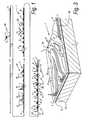
- Figure 1shows some steps in a method for manufacturing coated panels 1.
- the methodcomprises at least a step S1 in which the substrate 2 is printed.
- the print 4 from step S1 represented hereis performed indirectly on the substrate 2.
- this substrate 2then has been provided with one or more primer layers 5, such as uniform basic layers.
- Providing this basic layer or primer layer 5 in step S0comprises, in this example, at least providing a substance 6, such as a lacquer, in liquid form.
- the basic layermay also comprise solid layers, such as paper layers, or one may work without basic layer, such that in this latter case the print 4 is performed directly on the substrate 2.
- the particularity of the method of the exampleconsists in that during said step S1, in which the substrate 2 is printed, a structure 7 is realized on the substrate 2, wherein this structure 7 comprises protrusions 8 formed by two or more print layers 9 provided on top of each other.
- this structure 7comprises protrusions 8 formed by two or more print layers 9 provided on top of each other.
- Thisis realized here by moving the board-shaped substrate 2 beneath several printing units 10.
- These printing units 10may form part of the same or several printing devices.
- a transparent layer 11is provided on the board-shaped substrate 2, with which layer the print 4 is covered.
- the transparent or translucent layer 11is provided by means of a method in which at least a liquid substance 12 is provided on the substrate 2.
- various techniquesmay be applied, such as spraying techniques, pouring techniques, roller application techniques, and so on.
- a solid or already solidified transparent or translucent layer 11is used which is provided on the substrate 2.
- a so-called overlaywhich may consist of a material sheet provided with synthetic material, such as a paper layer soaked with melamine resin.
- step S1 and S2 in the exampleare performed on larger boards, which then are divided in a successive treatment step S3, it is not excluded that, according to variants, the step S1 and/or the step S2 are performed on smaller panels 13, which, for example, already have substantially the dimensions of the final coated panels 1.
- step S2 in the exampleis performed after step S1 has been completed, it is not excluded that, according to variants, a transparent or translucent layer 11 is used, which is provided in two or more partial steps, wherein at least one of these partial steps is performed before said printing step S1 is completed, for example, before applying at least one of said print layers 9.
- the transparent and/or translucent layer 11, which is provided in step S2 or in one or more partial steps of S2,does not necessarily have to cover the entire surface of the substrate 2 or the panel 1 obtained from it.
- the translucent or transparent layer 11may be provided in the spaces between one or more of the print layers 9 of the protrusions 8, which then already have or have not been provided on the substrate 2.
- the coated panels 1 which have been obtained after step S3possibly may undergo still further treatments, such as edge treatments.
- profiled edge portions comprising coupling meansmay be realized at the edges of these panels, by which the panels can be coupled to each other in order to form a floor covering.
- Thismay relate to coupling means in the form of a traditional tongue and groove connection, which then are glued together when installing the floor covering, or in the form of so-called glue-free mechanical connections, such as those known as such, for example, from WO 97/47834 .
- Figure 2shows a finished coated panel 1, in this case, a floor panel.
- thisrelates to an oblong floor panel, which both at the opposed long edges 14-15 and the opposed short edges 16-17 is provided with coupling means which substantially are made as a tongue 18 and a groove 19.
- the floor panelhas a decorative top layer 3 obtained by means of a method according to the invention.
- thisrelates to a decorative top layer 3 representing a wood pattern.
- the structure 7 realized by means of the methodrelates to a wood structure.
- such wood pattern and/or wood structuremay show elements such as wood nerves 21 and/or wood pores 22 and/or wood silver grains and/or wood knots 24 and the like.
- one or more of the elements from the wood patternmay correspond to the wood structure, by which is meant that the protrusions 8 of the structure 7 are situated along or at the height of the corresponding portion of the pattern or follow this pattern.
- the protrusions 8 of the structure 7 of the present inventionthen will leave just this wood pore blank and cover the surface next to this wood pore.
- the print layers 9may cover a smaller or a larger surface of the substrate 2.
- characteristic protrusions 8can be formed by means of the technique of the invention, whereas recesses are formed by means of a technique from the prior art, for example, by impressing a translucent or translucent layer 11, which is provided on top of the print layers 9, with a mould, and/or by working with a repellant for this layer 11, which repellant then is provided on the locations where the recess is expected.
- Said wood patternmay be obtained in any manner.
- thisrelates to a printed wood pattern, however, one may also work with a veneer layer or a cork layer.
- this print 25can have been provided beforehand on a material sheet, such as on a paper layer, or this print 25 may also, whether or not directly, be printed on the substrate 2, wherein printing the pattern then forms part of said step S1 in which the substrate 2 is printed.
- a substantially flat print 25can be obtained, which represents the wood pattern or a portion thereof, after which the print layers 9, which form the protrusions 8, are provided, or the print 25 of the pattern can be provided after already at least one or even all print layers 9 forming the protrusions 8 have been applied.
- Figure 3represents an example, wherein some wood nerves 21 are provided with a relief by providing each time two or more print layers 9 on top of each other. These are provided on a substrate 2, which is provided with a primer layer 5 and subsequently is printed with a wood pattern.
- the example from figure 3further also clearly shows that the structure 7 is provided in correspondence with the wood pattern and that the protrusions 8-8A which are present in the structure 7 may comprise a varying number of print layers 9.
- the protrusion 8A situated at the right hand side belowit is shown that the different print layers 9 forming one and the same protrusion 8A do not necessarily have to overlap each other completely. In this manner, truly three-dimensional protrusions 8A can be constructed.
- Figure 4shows an embodiment wherein a protrusion 8 is formed by four substantially identical print layers 9, above which a transparent or translucent layer 11 with hard particles 26 is provided.
- the formed protrusion 8remains tangibly present to a greater or lesser extent.
- the thickness of the transparent or translucent layer 11is smaller than the thickness or still better smaller than half of the thickness of the protrusion 8.
- Figure 5shows an embodiment, wherein a protrusion 8A is formed by four print layers 9 situated on top of each other and having a different cross-section, as a result of which this protrusion 8A, which is built up in layers, shows at least one inclined or curved wall 28.
- this protrusion 8Awhich is built up in layers, shows at least one inclined or curved wall 28.
- the cross-section of the print layers 9decreases from the substrate 2 towards the surface of the decorative top layer 3.
- the technique of the inventionalso allows realizing other edge characteristics, such as imitations of joints, cement joints and gaps. Also, it is possible to realize the already mentioned edge characteristics, such as chamfers, within the decorative top layer 3 of the substrate 2 and/or the final coated panels 1. Thus, for example, it is possible to imitate so-called multiplanks by means of the technique of the invention in an advantageous manner. Said multiplanks represent several parallel rows of wood planks on the same coated panel 1. Between the wood planks then a gap or chamfer can be realized in the aforementioned manner.
- Figure 6shows with a variant that the print layers 9 not necessarily have to decrease in cross-section, such as in figure 5 .
- print layers 9are applied having cross-sections increasing from the substrate 2 towards the surface of the decorative top layer 3.
- This variantallows a larger tolerance in respect to the correspondence of the positions of the different print layers 9, as a small deviation in an underlying print layer 9 is concealed by a larger print layer 9 provided on top thereof.
- Figure 7shows another variant, in which the print 25 of the actual pattern of the decorative top layer 3 is provided after the structure 7 of protrusions 8 has been printed.
- thisrelates to a pattern printed on the substrate 2, which pattern also is printed over the already formed structure 7.
- the layer structure of the protrusions 8-8Ais concealed.
- Figure 8represents an example of the realization of an edge characteristic 29 by means of a method of the invention. In this case, this concerns a rounded bevel at the edge 30 of the coated panel 1.
- the variants presented by means of the figures 3 through 8can be applied in the same coated panel 1. It is also clear that in the case of the embodiments of figures 3 to 6 and 8 , at least the uppermost print layer 9 of the respective protrusion 8-8A preferably has a decorative aspect, for example, is formed by means of a colorant. It is possible that the uppermost print layer 9, for example, in the case of figure 8 , as such shows a pattern, such as a wood pattern. However, it is also possible that the print layers 9 forming the protrusions 8-8A are transparent or translucent and therefore have little or no influence upon the visibility of underlying layers, such as underlying prints. Such underlying print may be formed by the print 25 of the actual pattern.
- the thickness of the layers and/or prints represented in the figuresis shown schematically and/or exaggerated. Also, the mutual relations between these layers are shown randomly and do not contain a restriction in respect to possible embodiments or the materials applied in these layers or prints. It is clear that in general the total thickness of the decorative top layer 3 may be less than 2 millimeters and even less than 1 millimeter, whereas the substrate 2, upon which the decorative top layer 3 is provided, may vary in thickness, for example, between 5 and 15 or even up to 25 millimeters.
- the entire print 4comprises the possible print 25 of the wood pattern as well as the print layers 9 provided on top of each other. It is also noted that the print layers 9 provided on top of each other, which form the protrusions 8-8A, do not necessarily have to be in direct mutual contact. Possibly, intermediate materials may be applied, such as materials promoting the mutual adherence of the various print layers 9 on each other.
- the decorative top layer 3consists of all layers or other material situated on top of the substrate 2. It is also clear that the protrusions 8-8A do not necessarily form a structure which is present at the surface of the final coated panel 1. In fact, it is the print 4 itself, and in particular the print layers 9 provided on top of each other, which shows the structure 7. Such structure 7 in fact may be partially or even entirely flattened out by layers situated on top thereof, such as a transparent or translucent layer 11. Preferably, such structure 7 indeed results in a structure which is present at the surface of the final coated panel 1-13.
Landscapes
- Life Sciences & Earth Sciences (AREA)
- Engineering & Computer Science (AREA)
- Wood Science & Technology (AREA)
- Laminated Bodies (AREA)
- Finishing Walls (AREA)
- Application Of Or Painting With Fluid Materials (AREA)
- Panels For Use In Building Construction (AREA)
- Floor Finish (AREA)
- Printing Methods (AREA)
Abstract
Description
- This invention relates to a method for manufacturing coated panels, as well as to coated panels.
- More particularly, the invention relates to a method for manufacturing panels of the type comprising at least a substrate and a decorative top layer provided on this substrate, wherein the method, in order to form at least a portion of said top layer, comprises a step in which the substrate is printed, whether or not by the intermediary of possible primer layers or other intermediate material, in particular intermediate material layers.
- Such panels are known as such, for example, from the patent documents
US 3,173,804 ,US 3,554,827 ,US 3,811,915 ,WO 01/48333 WO 01/47724 US 2004/026017 ,WO 2004/042168 andEP 1 872 959 - From the aforesaid patent documents, various methods are known for providing the surface of the panel with a structure. From
WO 2004/042168 , it is known to provide recesses in the substrate itself or in a primer layer and to perform a print on this structured substrate. FromWO 01/47725 US 3,811,915 andUS 3,554,827 , it is known to provide a lacquer-repelling agent on the print, such that the transparent lacquer layer subsequently provided thereon hardens selectively, such that a structure is formed on the final panel. FromWO 01/48333 WO 01/47724 - Each of the known techniques for realizing a structure requires a high accuracy when a certain degree of correspondence between the actual print and the structure has to be obtained. Moreover, the above-mentioned techniques leave much to be desired in respect to flexibility and/or in respect to feasible structures. Thus, for example, it is difficult to realize structures with acute angles by these techniques. The relatively strongly rounded portions, which are difficult to avoid in the state of the art, lead to an unnatural appearance of the respective structure.
- Also, obtaining deep structures is not simple with the known techniques.
- The present invention aims at an alternative method for manufacturing coated panels of the above-mentioned type and, according to various embodiments thereof, offers advantages in respect to the state of the art. To this aim, the invention relates to a method for manufacturing coated panels of the type comprising at least a substrate and a decorative top layer provided on this substrate, wherein the method, in order to form at least a portion of said top layer, comprises a step in which the substrate is printed, with the characteristic that during said step a structure is realized on the substrate, wherein said structure comprises protrusions which are formed by two or more prints or print layers provided on top of each other.
- Due to the fact that at least two prints or print layers are provided on top of each other, a level variance may be created in the top layer, whereby more complex and/or more pronounced structures can be obtained. Preferably, protrusions are used which are formed with 3 or more, for example, up to 10 prints provided on top of each other, which considerably enhances the depth resolution, while still obtaining an economical process. Of course, not necessarily all protrusions of the respective structure must be constructed of an equally high number of prints or print layers provided on top of each other. By varying the number of prints provided on top of each other depending on the protrusion, a larger variation in the respective structure may be obtained.
- It is noted that said protrusions can manifest themselves locally as well as rather relatively extended. It is possible that a protrusion substantially extends over the entire surface of the substrate and is interrupted at one or more locations only, such that it is rather the interruption that provides for said structure.
- According to a first preferred embodiment, said two or more prints or print layers provided on top of each other show an identical pattern in a cross-section of the respective protrusion. By this, it is meant that the respective protrusion, viewed in a local cross-section, consists of two or more prints or print layers covering each other substantially or even almost perfectly. This embodiment allows performing relatively large level variances, wherein the respective protrusion, at least in the respective cross-section, possibly may be provided with straight walls or relatively acute angles. Still better, the respective protrusion, for the major part thereof, has cross-sections in which said print layers cover each other substantially or even almost perfectly.
- According to a second preferred embodiment, said two or more prints or print layers provided on top of each other show a different pattern in a cross-section of the respective protrusion, wherein the print located on top preferably has a smaller printed surface. This means that, in the case of a smaller printed surface, the respective protrusion, viewed in a local cross-section, consists of two or more prints or print layers, which do not cover each other entirely. This preferred embodiment allows realizing protrusions with an inclined wall, which as such increases the number of possibly achievable structures. Still better, the respective protrusion, for the major part thereof, has cross-sections in which said print layers show a different pattern, in other words, a different printed surface. It is clear that according to another possible embodiment of this second preferred embodiment, the print or print layer lying on top may have a larger printed surface, as a result of which the underlying print layer possibly may be covered entirely.
- Of course, the above two preferred embodiments may be combined in the same coated panel or even in the same protrusion. By this is meant that the structure may be constructed by means of one or more protrusions having cross-sections with the features of the first preferred embodiment, as well as cross-sections with the features of the second preferred embodiment.
- Preferably, said two or more prints or print layers provided on top of each other are made of the same material. By this, it is obtained that the respective protrusion is homogeneously constructed. However, it is not excluded that the material in certain print layers is varied, for example, with the intention of obtaining a visible layer structure or a visible gradual color and/or tint variation in the respective protrusion.
- The method of the invention is preferably applied for manufacturing panels with a decorative top layer representing a wood pattern, wherein said structure then preferably relates to a wood structure. Of course, one may also work with stone patterns, fantasy patterns and respective structures. Still better, said structure corresponds to an underlying, also printed pattern, for example, to the aforementioned wood pattern.
- Preferably, the step in which the substrate is printed is performed by means of one or more digitally controlled inkjet printing units. The use of inkjet printing units for printing on substrates of panels is known as such, for example, from the already mentioned
WO 01/48333 EP 1 872 959 - Preferably, said method comprises a step in which the substrate is provided with a transparent or translucent layer, which is provided on top of said prints. Although it is not excluded that, by means of said layer, finally a flat surface is obtained, preferably at least a portion of the already formed protrusions, or even all of the protrusions, manifest themselves through said layer, such that they preferably remain tangibly and visibly present at the final surface of the decorative top layer. When one or several protrusions are completely flattened out by means of said layer, it is preferred that the built-up protrusions remain at least visibly present through said transparent or translucent layer. By means of such embodiment, particular depth effects still can be achieved without a structure effect on the final surface. Such depth effects are less sensitive to wear, as they are embedded and are not present at the surface of the coated panel as projecting wear-sensitive portions.
- It is noted that the above-mentioned transparent or translucent layer may comprise ingredients which protect the underlying print layers, such as hard particles which reduce possible wear or scratches, or ingredients which restrict the aging of the color of an underlying pattern, such as ingredients reducing the UV sensitivity of the pattern.
- Preferably, the method of the invention is applied for manufacturing floor panels. In such case, it is surely desirable to apply a transparent or translucent layer with hard particles, such as aluminum oxide or any other mineral.
- It is clear that the method of the invention can be applied to any substrate and that, for example, the material of the substrate or the size thereof is not restricted. Concerning the material, use can be made of wood or wood-based materials, such as particle board or MDF or HDF (Medium Density Fiberboard or High Density Fiberboard). Of course, the substrate can be treated prior to said printing step. For example, the substrate may be provided with one or more primer layers, such as adherence layers, paper layers or so-called bottom shades. Said bottom shades may form, for example, a whether or not uniform background color of the pattern.
- In general, the method of the invention preferably is performed on substrates showing already as much as possible the geometry of the final coated panel. In such case, namely, the stock of different semi-finished products may be reduced. Thus, preferably said substrate approximately has its final size and shape when said prints are provided.
- Preferably, one or more of said prints or print layers are performed with a colorant, such as ink or paint. In the case of ink, one may opt for a water-based ink as well as for an ink on solvent basis, wherein the water-based ink is preferable, as this leads to a more economic and environmentally friendly process.
- According to an alternative, one or more of said prints or print layers may be performed with a transparent or translucent material, such as with a lacquer or a varnish.
- Preferably, the method of the invention is applied for manufacturing coated panels, such as floor panels, with a decorative top layer representing a pattern, wherein the pattern is obtained substantially or exclusively by printing said substrate. By means of this preferred embodiment, thus, the pattern as well as the structure of the panel may be obtained by a printing process applied on the substrate, as a consequence of which a very versatile process can be obtained. Of course, here, too, one may work with intermediate layers or material, such as primer layers.
- It is clear that the present invention also relates to coated panels which are obtained or may be obtained by a method of the invention. Such panel, according to a portrait definition and independently of the method by which they are manufactured, can be defined as a coated panel of the type comprising at least a substrate and a decorative top layer provided on this substrate, with the characteristic that said decorative top layer comprises a structure of protrusions, wherein at least one of said protrusions consists of two or more prints or print layers provided on top of each other. To those skilled in the art, it is clear that the preferred embodiments mentioned in connection with the method of the invention lead to corresponding preferred structural features of the coated panel.
- With the intention of better showing the characteristics of the invention, hereafter, as an example without any limitative character, several preferred embodiments are described, with reference to the appended drawings, wherein:
Figure 1 schematically represents a number of steps in a method according to the invention;Figure 2 represents a coated panel according to the invention;Figure 3 , in perspective and at a larger scale, represents a view on the area indicated by F3 infigure 2 ;Figure 4 , at a larger scale, represents a schematic view on the area indicated by F4 infigure 1 ;Figures 5 to 7 , in a similar view asfigure 4 , represent variants; andFigure 8 , at a larger scale, represents a schematic view on the area indicated by F8 infigure 1 .Figure 1 shows some steps in a method for manufacturingcoated panels 1. Herein, one starts from a board-shapedsubstrate 2, on which a decorativetop layer 3 is provided. For forming saidtop layer 3, the method comprises at least a step S1 in which thesubstrate 2 is printed. Theprint 4 from step S1 represented here is performed indirectly on thesubstrate 2. In a preceding step S0, thissubstrate 2 then has been provided with one ormore primer layers 5, such as uniform basic layers. Providing this basic layer orprimer layer 5 in step S0 comprises, in this example, at least providing asubstance 6, such as a lacquer, in liquid form. According to another possibility, the basic layer may also comprise solid layers, such as paper layers, or one may work without basic layer, such that in this latter case theprint 4 is performed directly on thesubstrate 2.- The particularity of the method of the example consists in that during said step S1, in which the
substrate 2 is printed, astructure 7 is realized on thesubstrate 2, wherein thisstructure 7 comprisesprotrusions 8 formed by two ormore print layers 9 provided on top of each other. In the present case, each time more than three, namely four, prints orprint layers 9 are provided on top of each other in order to form theprotrusions 8. This is realized here by moving the board-shapedsubstrate 2 beneathseveral printing units 10. Theseprinting units 10 may form part of the same or several printing devices. Preferably, use is made ofdigital printing devices 10, such asinkjet printing devices 10. Namely, those allow mutually attuning the separately appliedprint layers 9 in a simpler manner, more particularly in order to mutually attune the position of the printing layers 9. It is not excluded that other printing techniques than inkjet printing are applied. Thus, for example, it is possible to work with screen printing, offset printing and the like. Possibly, one may also work with a combination of printing techniques, which techniques each deposit one or more of the print layers 9 on thesubstrate 2. - In a step S2, which here is performed after the printing step S1 has been completed, a
transparent layer 11 is provided on the board-shapedsubstrate 2, with which layer theprint 4 is covered. Various techniques may be applied to this aim. As shown here, the transparent ortranslucent layer 11 is provided by means of a method in which at least aliquid substance 12 is provided on thesubstrate 2. For providing aliquid substance 12, various techniques may be applied, such as spraying techniques, pouring techniques, roller application techniques, and so on. It is not excluded that instead of working with a liquid substance, a solid or already solidified transparent ortranslucent layer 11 is used which is provided on thesubstrate 2. Thus, for example, one may work with a so-called overlay, which may consist of a material sheet provided with synthetic material, such as a paper layer soaked with melamine resin. - Although step S1 and S2 in the example are performed on larger boards, which then are divided in a successive treatment step S3, it is not excluded that, according to variants, the step S1 and/or the step S2 are performed on
smaller panels 13, which, for example, already have substantially the dimensions of the finalcoated panels 1. - Although step S2 in the example is performed after step S1 has been completed, it is not excluded that, according to variants, a transparent or
translucent layer 11 is used, which is provided in two or more partial steps, wherein at least one of these partial steps is performed before said printing step S1 is completed, for example, before applying at least one of said print layers 9. - It is noted that the transparent and/or
translucent layer 11, which is provided in step S2 or in one or more partial steps of S2, does not necessarily have to cover the entire surface of thesubstrate 2 or thepanel 1 obtained from it. Thus, for example, the translucent ortransparent layer 11 may be provided in the spaces between one or more of the print layers 9 of theprotrusions 8, which then already have or have not been provided on thesubstrate 2. - It is obvious that the
coated panels 1 which have been obtained after step S3 possibly may undergo still further treatments, such as edge treatments. So, for example, in the case that floor panels are concerned, profiled edge portions comprising coupling means may be realized at the edges of these panels, by which the panels can be coupled to each other in order to form a floor covering. This may relate to coupling means in the form of a traditional tongue and groove connection, which then are glued together when installing the floor covering, or in the form of so-called glue-free mechanical connections, such as those known as such, for example, fromWO 97/47834 Figure 2 shows a finishedcoated panel 1, in this case, a floor panel. Herein, this relates to an oblong floor panel, which both at the opposed long edges 14-15 and the opposed short edges 16-17 is provided with coupling means which substantially are made as atongue 18 and agroove 19. At theupper side 20 or decorative side, the floor panel has a decorativetop layer 3 obtained by means of a method according to the invention. In this case, this relates to a decorativetop layer 3 representing a wood pattern. Thestructure 7 realized by means of the method relates to a wood structure. As is evident fromfigure 2 , such wood pattern and/or wood structure may show elements such aswood nerves 21 and/orwood pores 22 and/or wood silver grains and/orwood knots 24 and the like. By means of the method of the present invention, one or more of the elements from the wood pattern may correspond to the wood structure, by which is meant that theprotrusions 8 of thestructure 7 are situated along or at the height of the corresponding portion of the pattern or follow this pattern.- It is clear that, when characteristic recesses have to be formed at the surface of the decorative
top layer 3, such as it may be the case when imitatingwood pores 22, theprotrusions 8 of thestructure 7 of the present invention then will leave just this wood pore blank and cover the surface next to this wood pore. According to the desiredstructure 7, the print layers 9 may cover a smaller or a larger surface of thesubstrate 2. - It is not excluded that the inventive technique for forming the
structure 7 applied in the present method is combined with methods known from the prior art. Thus, for example,characteristic protrusions 8 can be formed by means of the technique of the invention, whereas recesses are formed by means of a technique from the prior art, for example, by impressing a translucent ortranslucent layer 11, which is provided on top of the print layers 9, with a mould, and/or by working with a repellant for thislayer 11, which repellant then is provided on the locations where the recess is expected. - Said wood pattern may be obtained in any manner. Preferably, this relates to a printed wood pattern, however, one may also work with a veneer layer or a cork layer. When the wood pattern is printed, this
print 25 can have been provided beforehand on a material sheet, such as on a paper layer, or thisprint 25 may also, whether or not directly, be printed on thesubstrate 2, wherein printing the pattern then forms part of said step S1 in which thesubstrate 2 is printed. Thus, for example, in this step first a substantiallyflat print 25 can be obtained, which represents the wood pattern or a portion thereof, after which the print layers 9, which form theprotrusions 8, are provided, or theprint 25 of the pattern can be provided after already at least one or even allprint layers 9 forming theprotrusions 8 have been applied. Figure 3 represents an example, wherein somewood nerves 21 are provided with a relief by providing each time two ormore print layers 9 on top of each other. These are provided on asubstrate 2, which is provided with aprimer layer 5 and subsequently is printed with a wood pattern. The example fromfigure 3 further also clearly shows that thestructure 7 is provided in correspondence with the wood pattern and that the protrusions 8-8A which are present in thestructure 7 may comprise a varying number of print layers 9. Also, by means of theprotrusion 8A situated at the right hand side below, it is shown that thedifferent print layers 9 forming one and thesame protrusion 8A do not necessarily have to overlap each other completely. In this manner, truly three-dimensional protrusions 8A can be constructed.- It is noted that in
figure 3 , for the sake of the simplicity of the representation, the possible translucent ortransparent layer 11 which can be provided oversuch panel 1 orsubstrate 2 is not shown here. Figure 4 shows an embodiment wherein aprotrusion 8 is formed by four substantiallyidentical print layers 9, above which a transparent ortranslucent layer 11 withhard particles 26 is provided. According to the thickness of thetranslucent layer 11, the formedprotrusion 8 remains tangibly present to a greater or lesser extent. The thinner thislayer 11 is provided above theprotrusion 8, the simpler is it to maintain thesharp edges 27 of thestructure 7 present at the surface of thecoated panel 1, too. Preferably, the thickness of the transparent ortranslucent layer 11 is smaller than the thickness or still better smaller than half of the thickness of theprotrusion 8.Figure 5 shows an embodiment, wherein aprotrusion 8A is formed by fourprint layers 9 situated on top of each other and having a different cross-section, as a result of which thisprotrusion 8A, which is built up in layers, shows at least one inclined orcurved wall 28. In the case offigure 5 , the cross-section of the print layers 9 decreases from thesubstrate 2 towards the surface of the decorativetop layer 3.- The possibility of realizing inclined or
curved walls 28 renders the technique of the invention also very suitable for realizing edge characteristics, such as deepened edges, for example, in the form of a bevel or chamfer. - The technique of the invention also allows realizing other edge characteristics, such as imitations of joints, cement joints and gaps. Also, it is possible to realize the already mentioned edge characteristics, such as chamfers, within the decorative
top layer 3 of thesubstrate 2 and/or the finalcoated panels 1. Thus, for example, it is possible to imitate so-called multiplanks by means of the technique of the invention in an advantageous manner. Said multiplanks represent several parallel rows of wood planks on the samecoated panel 1. Between the wood planks then a gap or chamfer can be realized in the aforementioned manner. Figure 6 shows with a variant that the print layers 9 not necessarily have to decrease in cross-section, such as infigure 5 . Infigure 6 ,print layers 9 are applied having cross-sections increasing from thesubstrate 2 towards the surface of the decorativetop layer 3. This variant allows a larger tolerance in respect to the correspondence of the positions of thedifferent print layers 9, as a small deviation in anunderlying print layer 9 is concealed by alarger print layer 9 provided on top thereof.Figure 7 shows another variant, in which theprint 25 of the actual pattern of the decorativetop layer 3 is provided after thestructure 7 ofprotrusions 8 has been printed. In this case, this relates to a pattern printed on thesubstrate 2, which pattern also is printed over the already formedstructure 7. By this is obtained that the layer structure of the protrusions 8-8A is concealed. Of course, instead of printing over the protrusions 8-8A, it is also possible to print theprint 25 of the actual pattern in between the protrusions 8-8A and/or that the protrusions 8-8A themselves are an integral part of the pattern. A combination of both printing methods for the pattern is possible, too.Figure 8 represents an example of the realization of an edge characteristic 29 by means of a method of the invention. In this case, this concerns a rounded bevel at theedge 30 of thecoated panel 1.- It is clear that the variants presented by means of the
figures 3 through 8 can be applied in the samecoated panel 1. It is also clear that in the case of the embodiments offigures 3 to 6 and8 , at least theuppermost print layer 9 of the respective protrusion 8-8A preferably has a decorative aspect, for example, is formed by means of a colorant. It is possible that theuppermost print layer 9, for example, in the case offigure 8 , as such shows a pattern, such as a wood pattern. However, it is also possible that the print layers 9 forming the protrusions 8-8A are transparent or translucent and therefore have little or no influence upon the visibility of underlying layers, such as underlying prints. Such underlying print may be formed by theprint 25 of the actual pattern. - It is noted that the thickness of the layers and/or prints represented in the figures is shown schematically and/or exaggerated. Also, the mutual relations between these layers are shown randomly and do not contain a restriction in respect to possible embodiments or the materials applied in these layers or prints. It is clear that in general the total thickness of the decorative
top layer 3 may be less than 2 millimeters and even less than 1 millimeter, whereas thesubstrate 2, upon which the decorativetop layer 3 is provided, may vary in thickness, for example, between 5 and 15 or even up to 25 millimeters. - Further, it is noted that the
entire print 4 comprises thepossible print 25 of the wood pattern as well as the print layers 9 provided on top of each other. It is also noted that the print layers 9 provided on top of each other, which form the protrusions 8-8A, do not necessarily have to be in direct mutual contact. Possibly, intermediate materials may be applied, such as materials promoting the mutual adherence of thevarious print layers 9 on each other. - It is clear that the decorative
top layer 3 consists of all layers or other material situated on top of thesubstrate 2. It is also clear that the protrusions 8-8A do not necessarily form a structure which is present at the surface of the finalcoated panel 1. In fact, it is theprint 4 itself, and in particular the print layers 9 provided on top of each other, which shows thestructure 7.Such structure 7 in fact may be partially or even entirely flattened out by layers situated on top thereof, such as a transparent ortranslucent layer 11. Preferably,such structure 7 indeed results in a structure which is present at the surface of the final coated panel 1-13. - The present invention is in no way limited to the herein above-described embodiments; on the contrary may such methods and coated panels be realized without deviating from the scope of the present invention.
Claims (15)
- Method for manufacturing coated panels of the type comprising at least a substrate (2) and a decorative top layer (3) provided on this substrate (2), wherein the method, in order to form at least a portion of said top layer (3), comprises a step (S1) in which the substrate (2) is printed,characterized in that during said step (S1) a structure (7) is realized on the substrate (2), wherein said structure (7) comprises protrusions (8-8A) formed by two or more prints (9) provided on top of each other.
- Method according to claim 1,characterized in that said two or more prints (9) provided on top of each other, in a cross-section of the respective protrusion, have an identical pattern.
- Method according to claim 1,characterized in that said two or more prints (9) provided on top of each other, in a cross-section of the respective protrusion, have a different pattern, wherein the print provided on top preferably has a smaller printed surface.
- Method according to any of the preceding claims,characterized in that said two or more prints (9) provided on top of each other are made of the same material.
- Method according to any of the preceding claims,characterized in that it is applied for manufacturing panels (1) with a decorative top layer (3) representing a wood pattern, wherein said structure (7) then relates to a wood structure.
- Method according to claim 5,characterized in that said wood structure corresponds to an underlying printed wood pattern.
- Method according to any of the preceding claims,characterized in that the step in which the substrate (2) is printed is performed by means of one or more digitally controlled inkjet printing units (10).
- Method according to any of the preceding claims,characterized in that said method comprises a step in which the substrate (2) is provided with a transparent or translucent layer (11), which is provided on top of said prints (9).
- Method according to any of the preceding claims,characterized in that it is applied for manufacturing floor panels.
- Method according to claim 9,characterized in that said substrate (2) has approximately its final size and shape when said prints (9) are applied.
- Method according to any of the preceding claims,characterized in that one or more of said prints (9) are performed with a colorant.
- Method according to claim 11,characterized in that one or more of said prints (9) are performed with a water-based ink or with an ink on solvent basis.
- Method according to any of the preceding claims,characterized in that one or more of the aforementioned prints (9) are performed with a transparent or translucent material.
- Method according to any of the preceding claims,characterized in that it is applied for manufacturing panels (1) with a decorative top layer (3) representing a pattern, wherein the pattern substantially or exclusively is obtained by printing said substrate (2).
- Coated panel,characterized in that it is obtained or may be obtained by means of a method according to any of the preceding claims.
Priority Applications (6)
| Application Number | Priority Date | Filing Date | Title |
|---|---|---|---|
| AT08006954TATE501863T1 (en) | 2008-04-08 | 2008-04-08 | METHOD FOR PRODUCING COATED PANELS AND COATED PANEL |
| DE602008005556TDE602008005556D1 (en) | 2008-04-08 | 2008-04-08 | Process for producing coated panels and coated panel |
| ES08006954TES2361513T3 (en) | 2008-04-08 | 2008-04-08 | METHOD FOR MANUFACTURING COVERED PANELS AND COVERED PANEL. |
| EP08006954AEP2108524B1 (en) | 2008-04-08 | 2008-04-08 | Method for manufacturing coated panels and coated panel |
| PL08006954TPL2108524T3 (en) | 2008-04-08 | 2008-04-08 | Method for manufacturing coated panels and coated panel |
| US12/404,070US8465804B2 (en) | 2008-04-08 | 2009-03-13 | Method for manufacturing coated panels |
Applications Claiming Priority (1)
| Application Number | Priority Date | Filing Date | Title |
|---|---|---|---|
| EP08006954AEP2108524B1 (en) | 2008-04-08 | 2008-04-08 | Method for manufacturing coated panels and coated panel |
Publications (2)
| Publication Number | Publication Date |
|---|---|
| EP2108524A1true EP2108524A1 (en) | 2009-10-14 |
| EP2108524B1 EP2108524B1 (en) | 2011-03-16 |
Family
ID=39543445
Family Applications (1)
| Application Number | Title | Priority Date | Filing Date |
|---|---|---|---|
| EP08006954AActiveEP2108524B1 (en) | 2008-04-08 | 2008-04-08 | Method for manufacturing coated panels and coated panel |
Country Status (6)
| Country | Link |
|---|---|
| US (1) | US8465804B2 (en) |
| EP (1) | EP2108524B1 (en) |
| AT (1) | ATE501863T1 (en) |
| DE (1) | DE602008005556D1 (en) |
| ES (1) | ES2361513T3 (en) |
| PL (1) | PL2108524T3 (en) |
Cited By (22)
| Publication number | Priority date | Publication date | Assignee | Title |
|---|---|---|---|---|
| EP2363299A1 (en)* | 2010-03-05 | 2011-09-07 | Spanolux N.V.- DIV. Balterio | A method of manufacturing a floor board |
| WO2012007230A1 (en) | 2010-07-16 | 2012-01-19 | Fritz Egger Gmbh & Co. Og | Method for producing a panel having a decorative finish and a three-dimensional structure |
| RU2470794C2 (en)* | 2009-12-23 | 2012-12-27 | Флоринг Текнолоджиз Лтд. | Method and device for refining particle board |
| WO2014014400A1 (en) | 2012-07-17 | 2014-01-23 | Floor Iptech Ab | See extra sheet |
| EP2722189A1 (en)* | 2012-10-17 | 2014-04-23 | Akzenta Paneele + Profile GmbH | Method for producing a decorated wall or floor panel |
| EP2851208A1 (en)* | 2013-09-24 | 2015-03-25 | Sika Technology AG | Floor with inlay pattern prepared by additive manufacturing techniques |
| EP2873535A1 (en)* | 2013-11-15 | 2015-05-20 | Flooring Technologies Ltd. | Workpieces with structured decorative surface |
| US9079212B2 (en) | 2013-01-11 | 2015-07-14 | Floor Iptech Ab | Dry ink for digital printing |
| EP2942207A1 (en)* | 2014-05-09 | 2015-11-11 | Flooring Technologies Ltd. | Method for producing decorated wood material boards and floor panel produced from the wood material board |
| EP3056350A1 (en)* | 2015-02-16 | 2016-08-17 | Wemhöner Surface Technologies GmbH & Co. KG | Method for creating a surface pattern on a surface of a workpiece and workpiece obtained thereby |
| US9446602B2 (en) | 2012-07-26 | 2016-09-20 | Ceraloc Innovation Ab | Digital binder printing |
| US10035358B2 (en) | 2012-07-17 | 2018-07-31 | Ceraloc Innovation Ab | Panels with digital embossed in register surface |
| US10041212B2 (en) | 2013-02-04 | 2018-08-07 | Ceraloc Innovation Ab | Digital overlay |
| CN111229567A (en)* | 2018-11-29 | 2020-06-05 | 彩碁科技股份有限公司 | Colored drawing substrate structure and manufacturing method thereof |
| IT201900011007A1 (en)* | 2019-07-05 | 2021-01-05 | Videografica Studio Srl | Relief decoration of panels through material stratification obtained with a digital process |
| US10899166B2 (en) | 2010-04-13 | 2021-01-26 | Valinge Innovation Ab | Digitally injected designs in powder surfaces |
| WO2021014307A1 (en) | 2019-07-22 | 2021-01-28 | Unilin, Bv | A floor panel having texture zones on the top surface |
| EP4063143A1 (en)* | 2021-03-26 | 2022-09-28 | Jesús Francisco Barberan Latorre | Method and system for producing reliefs on substrates |
| EP4134242A1 (en)* | 2021-08-09 | 2023-02-15 | Flooring Technologies Ltd. | Method and device for applying a decoration and a surface structure to a substrate |
| PL441700A1 (en)* | 2022-07-11 | 2024-01-15 | Decora Spółka Akcyjna | Decorative board with a synchronous structure |
| US11878324B2 (en) | 2013-01-11 | 2024-01-23 | Ceraloc Innovation Ab | Digital thermal binder and powder printing |
| WO2024089361A1 (en) | 2022-10-25 | 2024-05-02 | Gerflor | Process for manufacturing floor or wall coverings, and associated coverings |
Families Citing this family (36)
| Publication number | Priority date | Publication date | Assignee | Title |
|---|---|---|---|---|
| BE1016875A5 (en)* | 2005-12-23 | 2007-08-07 | Flooring Ind Ltd | FLOOR PANEL AND METHOD FOR MANUFACTURING SUCH FLOOR PANEL. |
| KR101616593B1 (en) | 2008-12-19 | 2016-05-12 | 플로어링 인더스트리즈 리미티드 에스에이알엘 | Coated panel comprising foam or polyvinyl chloride and method for manufacturing |
| BE1018680A5 (en) | 2008-12-19 | 2011-06-07 | Flooring Ind Ltd Sarl | METHODS FOR MANUFACTURING PANELS AND PANEL OBTAINED HEREBY |
| US8359794B2 (en)* | 2009-11-04 | 2013-01-29 | Walter Biro | Extruded plastic members for covering wood surfaces |
| PT2339092T (en) | 2009-12-22 | 2019-07-19 | Flooring Ind Ltd Sarl | Method for producing covering panels |
| US8925275B2 (en) | 2010-05-10 | 2015-01-06 | Flooring Industries Limited, Sarl | Floor panel |
| BE1019331A5 (en) | 2010-05-10 | 2012-06-05 | Flooring Ind Ltd Sarl | FLOOR PANEL AND METHODS FOR MANUFACTURING FLOOR PANELS. |
| BE1019501A5 (en) | 2010-05-10 | 2012-08-07 | Flooring Ind Ltd Sarl | FLOOR PANEL AND METHOD FOR MANUFACTURING FLOOR PANELS. |
| PL2402173T3 (en) | 2010-06-30 | 2013-07-31 | Flooring Technologies Ltd | Method for finishing a panel and device for implementing such a method |
| EP3492274B1 (en)* | 2012-09-14 | 2020-11-04 | Unilin, BV | A method of decorating a panel |
| NL2010375C2 (en) | 2013-02-28 | 2014-09-01 | Ihc Sea Steel Ltd | Pile driving guide. |
| US11077607B2 (en) | 2013-10-21 | 2021-08-03 | Made In Space, Inc. | Manufacturing in microgravity and varying external force environments |
| US10705509B2 (en) | 2013-10-21 | 2020-07-07 | Made In Space, Inc. | Digital catalog for manufacturing |
| DE102014100858B3 (en)* | 2014-01-27 | 2015-07-09 | Akzenta Paneele + Profile Gmbh | Method and device for producing a direct-printed decorative panel with reduction of rejects due to printing errors |
| PT3323628T (en) | 2014-02-25 | 2022-08-19 | Akzenta Paneele Profile Gmbh | Method for producing decorative panels |
| JP6601920B2 (en)* | 2014-09-21 | 2019-11-06 | メイド イン スペース インコーポレイティッド | Ground and space installation manufacturing systems |
| KR102513809B1 (en) | 2016-09-23 | 2023-03-24 | 쇼 인더스트리즈 그룹, 인코포레이티드 | Resilient flooring products and manufacturing methods thereof |
| NL2017560B1 (en) | 2016-09-30 | 2018-04-10 | Ihc Iqip Uk Ltd | Pile guide comprising a base frame and a guide member |
| US10836108B1 (en) | 2017-06-30 | 2020-11-17 | Made In Space, Inc. | System and method for monitoring and inspection of feedstock material for direct feedback into a deposition process |
| BE1025875B1 (en) | 2018-01-04 | 2019-08-06 | Unilin Bvba | Methods for manufacturing panels |
| US12325259B2 (en) | 2018-03-14 | 2025-06-10 | Unilin, Bv | Methods for manufacturing decorative panels and panels obtainable thereby |
| JP7196510B2 (en) | 2018-09-28 | 2022-12-27 | 大日本印刷株式会社 | Embossed wood grain decorative material |
| EP3778259A4 (en)* | 2018-03-30 | 2021-12-08 | Dai Nippon Printing Co., Ltd. | DECORATIVE MATERIAL WITH RAISED WOOD GRAIN |
| JP7279321B2 (en)* | 2018-03-30 | 2023-05-23 | 大日本印刷株式会社 | Embossed wood grain decorative material |
| KR20250012747A (en)* | 2018-03-30 | 2025-01-24 | 다이니폰 인사츠 가부시키가이샤 | Raised woodgrain finish decorative material |
| US11203224B2 (en) | 2018-08-30 | 2021-12-21 | Interface, Inc. | Digital printing for flooring and decorative structures |
| CN114423620B (en)* | 2019-09-27 | 2023-06-20 | 大日本印刷株式会社 | decorative material |
| CN110696516A (en)* | 2019-10-12 | 2020-01-17 | 浙江晶通塑胶有限公司 | Processing technology of digital printing floor |
| RU2745545C1 (en)* | 2020-03-13 | 2021-03-26 | Общество с ограниченной ответственностью "3Д-Реплика" (ООО - 3Д-Реплика") | Decorative device with an applied relief image and a method for obtaining a relief image |
| WO2022115462A2 (en)* | 2020-11-24 | 2022-06-02 | Aladdin Manufacturing Corporation | Floor panel and methods for manufacturing floor panels |
| IT202100008192A1 (en) | 2021-04-01 | 2022-10-01 | Giorgio Macor | METHOD TO DECORATE A MATERIAL |
| US20240116307A1 (en) | 2020-12-29 | 2024-04-11 | Giorgio Macor | Method providing a workpiece with a three-dimensionally textured surface coating |
| US20230383546A1 (en)* | 2020-12-31 | 2023-11-30 | Zhejiang Yongyu Furniture Co., Ltd. | Multi-layer co-extrusion stone plastic floors and manufacturing methods thereof |
| NL2027548B1 (en)* | 2021-02-12 | 2022-09-12 | I4F Licensing Nv | Decorative panel, and decorative panel covering |
| IT202200015618A1 (en) | 2022-07-25 | 2024-01-25 | Giorgio Macor | Method for generating a decoration that can be peeled off on command and product thus obtained. |
| CN117980151A (en)* | 2022-08-10 | 2024-05-03 | 努尔墨水创新有限公司 | Printing process for producing textured images |
Citations (11)
| Publication number | Priority date | Publication date | Assignee | Title |
|---|---|---|---|---|
| US3173804A (en) | 1960-12-16 | 1965-03-16 | Renkl Paidiwerk | Apparatus for applying a surface pattern on boards of wood, fiberboard, or the like |
| US3554827A (en) | 1968-11-12 | 1971-01-12 | Eidai Co Ltd | Method of forming a decorative panel |
| US3811915A (en) | 1971-04-27 | 1974-05-21 | Inmont Corp | Printing method for forming three dimensional simulated wood grain,and product formed thereby |
| US3905849A (en)* | 1972-08-31 | 1975-09-16 | Eurofloor Sa | Textured sheet material and method of preparation thereof |
| US4050409A (en)* | 1973-10-24 | 1977-09-27 | Alain Duchenaud | Cylinder for reproducing raised patterns on all surfaces |
| WO1997047834A1 (en) | 1996-06-11 | 1997-12-18 | Unilin Beheer B.V. | Floor covering, consisting of hard floor panels and method for manufacturing such floor panels |
| WO2001047725A1 (en) | 1999-12-23 | 2001-07-05 | Perstorp Flooring Ab | A process for the manufacturing of surface elements with a structured upper surface |
| FR2827529A1 (en)* | 2001-07-20 | 2003-01-24 | Rexam Beaute Metallisation | Article with coating imitating droplets for cosmetics packaging, uses liquid which is printed onto surface of article and then dries to form a pattern resembling liquid droplets |
| US20040026017A1 (en) | 2002-08-07 | 2004-02-12 | Taylor Dene H. | Method and system for producing a wood substrate having an image on at least one surface and the resulting wood product |
| WO2004042168A1 (en) | 2002-11-01 | 2004-05-21 | Mannington Mills, Inc. | A surface covering panel with printed pattern |
| EP1872959A1 (en) | 2006-06-26 | 2008-01-02 | Dante Frati | Process for printing surfaces of wood-based flat elements |
Family Cites Families (6)
| Publication number | Priority date | Publication date | Assignee | Title |
|---|---|---|---|---|
| US3810774A (en)* | 1972-04-17 | 1974-05-14 | Masonite Corp | Multi-color,multi-patterned panels |
| US4097635A (en)* | 1976-12-27 | 1978-06-27 | Eucatex, S.A. | Decorative panel |
| US4233343A (en)* | 1978-08-10 | 1980-11-11 | J. J. Barker Company Limited | Three-dimensional decorative surface |
| JPH0655918B2 (en)* | 1989-04-21 | 1994-07-27 | アドガー工業株式会社 | White ink composition |
| US6477948B1 (en)* | 2000-08-14 | 2002-11-12 | The Proctor & Gamble Company | Means for enhancing print color density |
| US6979487B2 (en)* | 2001-03-27 | 2005-12-27 | Serigraph Inc. | Glossy printed article and method of manufacturing same |
- 2008
- 2008-04-08PLPL08006954Tpatent/PL2108524T3/enunknown
- 2008-04-08DEDE602008005556Tpatent/DE602008005556D1/enactiveActive
- 2008-04-08EPEP08006954Apatent/EP2108524B1/enactiveActive
- 2008-04-08ESES08006954Tpatent/ES2361513T3/enactiveActive
- 2008-04-08ATAT08006954Tpatent/ATE501863T1/enactive
- 2009
- 2009-03-13USUS12/404,070patent/US8465804B2/enactiveActive
Patent Citations (13)
| Publication number | Priority date | Publication date | Assignee | Title |
|---|---|---|---|---|
| US3173804A (en) | 1960-12-16 | 1965-03-16 | Renkl Paidiwerk | Apparatus for applying a surface pattern on boards of wood, fiberboard, or the like |
| US3554827A (en) | 1968-11-12 | 1971-01-12 | Eidai Co Ltd | Method of forming a decorative panel |
| US3811915A (en) | 1971-04-27 | 1974-05-21 | Inmont Corp | Printing method for forming three dimensional simulated wood grain,and product formed thereby |
| US3905849A (en)* | 1972-08-31 | 1975-09-16 | Eurofloor Sa | Textured sheet material and method of preparation thereof |
| US4050409A (en)* | 1973-10-24 | 1977-09-27 | Alain Duchenaud | Cylinder for reproducing raised patterns on all surfaces |
| WO1997047834A1 (en) | 1996-06-11 | 1997-12-18 | Unilin Beheer B.V. | Floor covering, consisting of hard floor panels and method for manufacturing such floor panels |
| WO2001047725A1 (en) | 1999-12-23 | 2001-07-05 | Perstorp Flooring Ab | A process for the manufacturing of surface elements with a structured upper surface |
| WO2001048333A1 (en) | 1999-12-23 | 2001-07-05 | Perstorp Flooring Ab | A process for the manufacturing of surface elements |
| WO2001047724A1 (en) | 1999-12-23 | 2001-07-05 | Perstorp Flooring Ab | A process for the manufacturing of surface elements with a structured top surface |
| FR2827529A1 (en)* | 2001-07-20 | 2003-01-24 | Rexam Beaute Metallisation | Article with coating imitating droplets for cosmetics packaging, uses liquid which is printed onto surface of article and then dries to form a pattern resembling liquid droplets |
| US20040026017A1 (en) | 2002-08-07 | 2004-02-12 | Taylor Dene H. | Method and system for producing a wood substrate having an image on at least one surface and the resulting wood product |
| WO2004042168A1 (en) | 2002-11-01 | 2004-05-21 | Mannington Mills, Inc. | A surface covering panel with printed pattern |
| EP1872959A1 (en) | 2006-06-26 | 2008-01-02 | Dante Frati | Process for printing surfaces of wood-based flat elements |
Cited By (68)
| Publication number | Priority date | Publication date | Assignee | Title |
|---|---|---|---|---|
| RU2470794C2 (en)* | 2009-12-23 | 2012-12-27 | Флоринг Текнолоджиз Лтд. | Method and device for refining particle board |
| US11292289B2 (en) | 2010-03-05 | 2022-04-05 | Flooring Industries Limited, Sarl | Method of manufacturing a floor board |
| WO2011107610A1 (en)* | 2010-03-05 | 2011-09-09 | Spanolux N.V.- Div. Balterio | A method of manufacturing a floor board |
| US10239346B2 (en) | 2010-03-05 | 2019-03-26 | Unilin Bvba | Method of manufacturing a floor board |
| EP2363299A1 (en)* | 2010-03-05 | 2011-09-07 | Spanolux N.V.- DIV. Balterio | A method of manufacturing a floor board |
| US11970020B2 (en) | 2010-03-05 | 2024-04-30 | Unilin Bv | Method for manufacturing a floor board |
| US11938751B2 (en) | 2010-03-05 | 2024-03-26 | Flooring Industies Limited, Sarl | Method for manufacturing a floor board |
| US10899166B2 (en) | 2010-04-13 | 2021-01-26 | Valinge Innovation Ab | Digitally injected designs in powder surfaces |
| WO2012007230A1 (en) | 2010-07-16 | 2012-01-19 | Fritz Egger Gmbh & Co. Og | Method for producing a panel having a decorative finish and a three-dimensional structure |
| RU2531813C2 (en)* | 2010-07-16 | 2014-10-27 | Фриц Эггер Гмбх Унд Ко. Ог | Method to manufacture panel for furniture or floor |
| US10556447B2 (en) | 2012-07-17 | 2020-02-11 | Ceraloc Innovation Ab | Digital embossed in register surface |
| US11833846B2 (en) | 2012-07-17 | 2023-12-05 | Ceraloc Innovation Ab | Digital embossed in register surface |
| EP3626478A1 (en) | 2012-07-17 | 2020-03-25 | Ceraloc Innovation AB | Digital embossed in register surface |
| WO2014014400A1 (en) | 2012-07-17 | 2014-01-23 | Floor Iptech Ab | See extra sheet |
| US10035358B2 (en) | 2012-07-17 | 2018-07-31 | Ceraloc Innovation Ab | Panels with digital embossed in register surface |
| US11065889B2 (en) | 2012-07-26 | 2021-07-20 | Ceraloc Innovation Ab | Digital binder printing |
| US10016988B2 (en) | 2012-07-26 | 2018-07-10 | Ceraloc Innovation Ab | Digital binder printing |
| US10414173B2 (en) | 2012-07-26 | 2019-09-17 | Ceraloc Innovation Ab | Digital binder printing |
| US9446602B2 (en) | 2012-07-26 | 2016-09-20 | Ceraloc Innovation Ab | Digital binder printing |
| EP2909038A1 (en)* | 2012-10-17 | 2015-08-26 | Akzenta Paneele + Profile GmbH | Method for producing a decorated wall or floor panel |
| EP2722189A1 (en)* | 2012-10-17 | 2014-04-23 | Akzenta Paneele + Profile GmbH | Method for producing a decorated wall or floor panel |
| US9371456B2 (en) | 2013-01-11 | 2016-06-21 | Ceraloc Innovation Ab | Digital thermal binder and powder printing |
| US10800186B2 (en) | 2013-01-11 | 2020-10-13 | Ceraloc Innovation Ab | Digital printing with transparent blank ink |
| US9873803B2 (en) | 2013-01-11 | 2018-01-23 | Ceraloc Innovation Ab | Dry ink for digital printing |
| US9670371B2 (en) | 2013-01-11 | 2017-06-06 | Ceraloc Innovation Ab | Digital thermal binder and powder printing |
| US10029484B2 (en) | 2013-01-11 | 2018-07-24 | Ceraloc Innovation Ab | Digital embossing |
| US9630404B2 (en) | 2013-01-11 | 2017-04-25 | Ceraloc Innovation Ab | Dry ink for digital printing |
| US12172186B2 (en) | 2013-01-11 | 2024-12-24 | Ceraloc Innovation Ab | Method of forming a digital print with dry powder |
| US9079212B2 (en) | 2013-01-11 | 2015-07-14 | Floor Iptech Ab | Dry ink for digital printing |
| US11285508B2 (en) | 2013-01-11 | 2022-03-29 | Ceraloc Innovation Ab | Digital thermal binder and powder printing |
| US10189281B2 (en) | 2013-01-11 | 2019-01-29 | Ceraloc Innovation Ab | Digital thermal binder and power printing |
| US9528011B2 (en) | 2013-01-11 | 2016-12-27 | Ceraloc Innovation Ab | Digital binder and powder print |
| US10369814B2 (en) | 2013-01-11 | 2019-08-06 | Ceraloc Innovations Ab | Digital embossing |
| US10384471B2 (en) | 2013-01-11 | 2019-08-20 | Ceraloc Innovation Ab | Digital binder and powder print |
| US11130352B2 (en) | 2013-01-11 | 2021-09-28 | Ceraloc Innovation Ab | Digital binder and powder print |
| US9321925B2 (en) | 2013-01-11 | 2016-04-26 | Floor Iptech Ab | Dry ink for digital printing |
| US10596837B2 (en) | 2013-01-11 | 2020-03-24 | Ceraloc Innovation Ab | Digital thermal binder and powder printing |
| US9279058B2 (en) | 2013-01-11 | 2016-03-08 | Floor Iptech Ab | Digital embossing |
| US11014378B2 (en) | 2013-01-11 | 2021-05-25 | Ceraloc Innovation Ab | Digital embossing |
| US10723147B2 (en) | 2013-01-11 | 2020-07-28 | Ceraloc Innovation Ab | Digital thermal binder and powder printing |
| US11878324B2 (en) | 2013-01-11 | 2024-01-23 | Ceraloc Innovation Ab | Digital thermal binder and powder printing |
| US9738095B2 (en) | 2013-01-11 | 2017-08-22 | Ceraloc Innovation Ab | Digital printing with transparent blank ink |
| US12318808B2 (en) | 2013-01-11 | 2025-06-03 | Ceraloc Innovation Ab | Digital printing with transparent blank ink |
| US10041212B2 (en) | 2013-02-04 | 2018-08-07 | Ceraloc Innovation Ab | Digital overlay |
| US10988901B2 (en) | 2013-02-04 | 2021-04-27 | Ceraloc Innovation Ab | Digital overlay |
| US11566380B2 (en) | 2013-02-04 | 2023-01-31 | Ceraloc Innovation Ab | Digital overlay |
| WO2015044046A1 (en)* | 2013-09-24 | 2015-04-02 | Sika Technology Ag | Floor with inlay pattern prepared by additive manufacturing techniques |
| EP2851208A1 (en)* | 2013-09-24 | 2015-03-25 | Sika Technology AG | Floor with inlay pattern prepared by additive manufacturing techniques |
| EP2873535A1 (en)* | 2013-11-15 | 2015-05-20 | Flooring Technologies Ltd. | Workpieces with structured decorative surface |
| US10059030B2 (en) | 2014-05-09 | 2018-08-28 | Flooring Technologies Ltd. | Method for producing decorated wooden composite boards and panel produced from the wooden composite board, in particular floor panel, and use of a wooden composite board produced according to the method |
| EP3378675A1 (en)* | 2014-05-09 | 2018-09-26 | Flooring Technologies Ltd. | Method for producing decorated wood material boards and floor panel made from the wood material board |
| WO2015169450A1 (en)* | 2014-05-09 | 2015-11-12 | Flooring Technologies Ltd. | Method for producing decorated wooden composite boards and panel produced from the wooden composite board, in particular floor panel, and use of a wooden composite board produced according to the method |
| EP2942207A1 (en)* | 2014-05-09 | 2015-11-11 | Flooring Technologies Ltd. | Method for producing decorated wood material boards and floor panel produced from the wood material board |
| EP3056350A1 (en)* | 2015-02-16 | 2016-08-17 | Wemhöner Surface Technologies GmbH & Co. KG | Method for creating a surface pattern on a surface of a workpiece and workpiece obtained thereby |
| US11491761B2 (en) | 2018-11-29 | 2022-11-08 | Printgoal Technology Co., Ltd. | Colorful board structure and manufacturing method thereof |
| CN111229567A (en)* | 2018-11-29 | 2020-06-05 | 彩碁科技股份有限公司 | Colored drawing substrate structure and manufacturing method thereof |
| US11590733B2 (en) | 2018-11-29 | 2023-02-28 | Printgoal Technology Co., Ltd. | Colorful board structure and manufacturing method thereof |
| EP3838581A1 (en)* | 2019-07-05 | 2021-06-23 | Videografica Studio S.r.l. | Relief decoration for panels made through tactile stratification obtained by digital processing |
| IT201900011007A1 (en)* | 2019-07-05 | 2021-01-05 | Videografica Studio Srl | Relief decoration of panels through material stratification obtained with a digital process |
| BE1027454A1 (en) | 2019-07-22 | 2021-02-15 | Unilin Bv | A floor panel |
| US12203277B2 (en) | 2019-07-22 | 2025-01-21 | Unilin Bv | Floor panel |
| WO2021014307A1 (en) | 2019-07-22 | 2021-01-28 | Unilin, Bv | A floor panel having texture zones on the top surface |
| US11833848B2 (en) | 2021-03-26 | 2023-12-05 | Jesus Francisco Barberan Latorre | Method and system for producing reliefs on substrates |
| EP4063143A1 (en)* | 2021-03-26 | 2022-09-28 | Jesús Francisco Barberan Latorre | Method and system for producing reliefs on substrates |
| WO2023017024A1 (en)* | 2021-08-09 | 2023-02-16 | Flooring Technologies Ltd. | Method and device for applying a decoration and a surface structure to a carrier material |
| EP4134242A1 (en)* | 2021-08-09 | 2023-02-15 | Flooring Technologies Ltd. | Method and device for applying a decoration and a surface structure to a substrate |
| PL441700A1 (en)* | 2022-07-11 | 2024-01-15 | Decora Spółka Akcyjna | Decorative board with a synchronous structure |
| WO2024089361A1 (en) | 2022-10-25 | 2024-05-02 | Gerflor | Process for manufacturing floor or wall coverings, and associated coverings |
Also Published As
| Publication number | Publication date |
|---|---|
| DE602008005556D1 (en) | 2011-04-28 |
| EP2108524B1 (en) | 2011-03-16 |
| ATE501863T1 (en) | 2011-04-15 |
| US20090252925A1 (en) | 2009-10-08 |
| PL2108524T3 (en) | 2011-07-29 |
| ES2361513T3 (en) | 2011-06-17 |
| US8465804B2 (en) | 2013-06-18 |
Similar Documents
| Publication | Publication Date | Title |
|---|---|---|
| EP2108524B1 (en) | Method for manufacturing coated panels and coated panel | |
| DE102005046264B4 (en) | Method for producing a panel with a surface coating | |
| RU2531813C2 (en) | Method to manufacture panel for furniture or floor | |
| EP1973751B1 (en) | Floor panel having a wood imitating pattern and method for manufacturing | |
| US7249445B2 (en) | Floor covering, floor panels for forming such floor covering, and method of realizing such floor panels | |
| RU2526009C2 (en) | Production of floor panel and floor panel thus made | |
| DE60015603T2 (en) | METHOD FOR PRODUCING SURFACE ELEMENTS | |
| US12251916B2 (en) | Methods for manufacturing panels | |
| BE1018696A3 (en) | METHOD FOR MANUFACTURING PANELS AND PANELS OBTAINED HEREBY | |
| EP2133215B1 (en) | Method for manufacturing panels | |
| EP1838936B1 (en) | Cladding formed by panels having a strip flooring look | |
| US20060144004A1 (en) | Floor panel and method for manufacturing a floor panel | |
| BE1018337A3 (en) | METHODS FOR MANUFACTURING PANELS AND PANEL OBTAINED HEREBY | |
| EP4159469A1 (en) | Laminate panel, method for manufacturing a laminate panel and press element for realizing the method | |
| EP1918095B1 (en) | Composite wood board with real wood veneer and processing method | |
| BE1016394A3 (en) | FLOOR PANEL, AND METHOD, DEVICE AND ACCESSORIES FOR MANUFACTURING SUCH FLOOR PANEL. | |
| EP3470972B1 (en) | Method for the repeated use of digital print data for generating optically and/or haptically high value printed decorations on a substrate | |
| US20230056626A1 (en) | Pressing element and method for manufacturing pressing elements | |
| KR20060004828A (en) | Floorboard and its manufacturing method | |
| KR200364191Y1 (en) | Floor board | |
| WO2025056746A1 (en) | Floor panel with joint, floor panel arrangement and production method |
Legal Events
| Date | Code | Title | Description |
|---|---|---|---|
| PUAI | Public reference made under article 153(3) epc to a published international application that has entered the european phase | Free format text:ORIGINAL CODE: 0009012 | |
| 17P | Request for examination filed | Effective date:20090213 | |
| AK | Designated contracting states | Kind code of ref document:A1 Designated state(s):AT BE BG CH CY CZ DE DK EE ES FI FR GB GR HR HU IE IS IT LI LT LU LV MC MT NL NO PL PT RO SE SI SK TR | |
| AX | Request for extension of the european patent | Extension state:AL BA MK RS | |
| AKX | Designation fees paid | Designated state(s):AT BE BG CH CY CZ DE DK EE ES FI FR GB GR HR HU IE IS IT LI LT LU LV MC MT NL NO PL PT RO SE SI SK TR | |
| GRAP | Despatch of communication of intention to grant a patent | Free format text:ORIGINAL CODE: EPIDOSNIGR1 | |
| GRAS | Grant fee paid | Free format text:ORIGINAL CODE: EPIDOSNIGR3 | |
| GRAA | (expected) grant | Free format text:ORIGINAL CODE: 0009210 | |
| AK | Designated contracting states | Kind code of ref document:B1 Designated state(s):AT BE BG CH CY CZ DE DK EE ES FI FR GB GR HR HU IE IS IT LI LT LU LV MC MT NL NO PL PT RO SE SI SK TR | |
| REG | Reference to a national code | Ref country code:GB Ref legal event code:FG4D | |
| REG | Reference to a national code | Ref country code:CH Ref legal event code:EP | |
| REG | Reference to a national code | Ref country code:IE Ref legal event code:FG4D | |
| REF | Corresponds to: | Ref document number:602008005556 Country of ref document:DE Date of ref document:20110428 Kind code of ref document:P | |
| REG | Reference to a national code | Ref country code:DE Ref legal event code:R096 Ref document number:602008005556 Country of ref document:DE Effective date:20110428 | |
| REG | Reference to a national code | Ref country code:SE Ref legal event code:TRGR | |
| REG | Reference to a national code | Ref country code:ES Ref legal event code:FG2A Ref document number:2361513 Country of ref document:ES Kind code of ref document:T3 Effective date:20110617 | |
| REG | Reference to a national code | Ref country code:NL Ref legal event code:T3 | |
| PG25 | Lapsed in a contracting state [announced via postgrant information from national office to epo] | Ref country code:GR Free format text:LAPSE BECAUSE OF FAILURE TO SUBMIT A TRANSLATION OF THE DESCRIPTION OR TO PAY THE FEE WITHIN THE PRESCRIBED TIME-LIMIT Effective date:20110617 Ref country code:LT Free format text:LAPSE BECAUSE OF FAILURE TO SUBMIT A TRANSLATION OF THE DESCRIPTION OR TO PAY THE FEE WITHIN THE PRESCRIBED TIME-LIMIT Effective date:20110316 Ref country code:LV Free format text:LAPSE BECAUSE OF FAILURE TO SUBMIT A TRANSLATION OF THE DESCRIPTION OR TO PAY THE FEE WITHIN THE PRESCRIBED TIME-LIMIT Effective date:20110316 Ref country code:NO Free format text:LAPSE BECAUSE OF FAILURE TO SUBMIT A TRANSLATION OF THE DESCRIPTION OR TO PAY THE FEE WITHIN THE PRESCRIBED TIME-LIMIT Effective date:20110616 Ref country code:HR Free format text:LAPSE BECAUSE OF FAILURE TO SUBMIT A TRANSLATION OF THE DESCRIPTION OR TO PAY THE FEE WITHIN THE PRESCRIBED TIME-LIMIT Effective date:20110316 | |
| REG | Reference to a national code | Ref country code:PL Ref legal event code:T3 | |
| LTIE | Lt: invalidation of european patent or patent extension | Effective date:20110316 | |
| PG25 | Lapsed in a contracting state [announced via postgrant information from national office to epo] | Ref country code:FI Free format text:LAPSE BECAUSE OF FAILURE TO SUBMIT A TRANSLATION OF THE DESCRIPTION OR TO PAY THE FEE WITHIN THE PRESCRIBED TIME-LIMIT Effective date:20110316 Ref country code:SI Free format text:LAPSE BECAUSE OF FAILURE TO SUBMIT A TRANSLATION OF THE DESCRIPTION OR TO PAY THE FEE WITHIN THE PRESCRIBED TIME-LIMIT Effective date:20110316 Ref country code:CY Free format text:LAPSE BECAUSE OF FAILURE TO SUBMIT A TRANSLATION OF THE DESCRIPTION OR TO PAY THE FEE WITHIN THE PRESCRIBED TIME-LIMIT Effective date:20110316 Ref country code:BG Free format text:LAPSE BECAUSE OF FAILURE TO SUBMIT A TRANSLATION OF THE DESCRIPTION OR TO PAY THE FEE WITHIN THE PRESCRIBED TIME-LIMIT Effective date:20110616 | |
| PG25 | Lapsed in a contracting state [announced via postgrant information from national office to epo] | Ref country code:EE Free format text:LAPSE BECAUSE OF FAILURE TO SUBMIT A TRANSLATION OF THE DESCRIPTION OR TO PAY THE FEE WITHIN THE PRESCRIBED TIME-LIMIT Effective date:20110316 Ref country code:PT Free format text:LAPSE BECAUSE OF FAILURE TO SUBMIT A TRANSLATION OF THE DESCRIPTION OR TO PAY THE FEE WITHIN THE PRESCRIBED TIME-LIMIT Effective date:20110718 | |
| PG25 | Lapsed in a contracting state [announced via postgrant information from national office to epo] | Ref country code:MC Free format text:LAPSE BECAUSE OF NON-PAYMENT OF DUE FEES Effective date:20110430 Ref country code:IS Free format text:LAPSE BECAUSE OF FAILURE TO SUBMIT A TRANSLATION OF THE DESCRIPTION OR TO PAY THE FEE WITHIN THE PRESCRIBED TIME-LIMIT Effective date:20110716 Ref country code:SK Free format text:LAPSE BECAUSE OF FAILURE TO SUBMIT A TRANSLATION OF THE DESCRIPTION OR TO PAY THE FEE WITHIN THE PRESCRIBED TIME-LIMIT Effective date:20110316 Ref country code:RO Free format text:LAPSE BECAUSE OF FAILURE TO SUBMIT A TRANSLATION OF THE DESCRIPTION OR TO PAY THE FEE WITHIN THE PRESCRIBED TIME-LIMIT Effective date:20110316 Ref country code:CZ Free format text:LAPSE BECAUSE OF FAILURE TO SUBMIT A TRANSLATION OF THE DESCRIPTION OR TO PAY THE FEE WITHIN THE PRESCRIBED TIME-LIMIT Effective date:20110316 | |
| PG25 | Lapsed in a contracting state [announced via postgrant information from national office to epo] | Ref country code:MT Free format text:LAPSE BECAUSE OF FAILURE TO SUBMIT A TRANSLATION OF THE DESCRIPTION OR TO PAY THE FEE WITHIN THE PRESCRIBED TIME-LIMIT Effective date:20110316 | |
| PLBE | No opposition filed within time limit | Free format text:ORIGINAL CODE: 0009261 | |
| STAA | Information on the status of an ep patent application or granted ep patent | Free format text:STATUS: NO OPPOSITION FILED WITHIN TIME LIMIT | |
| REG | Reference to a national code | Ref country code:IE Ref legal event code:MM4A | |
| 26N | No opposition filed | Effective date:20111219 | |
| PG25 | Lapsed in a contracting state [announced via postgrant information from national office to epo] | Ref country code:DK Free format text:LAPSE BECAUSE OF FAILURE TO SUBMIT A TRANSLATION OF THE DESCRIPTION OR TO PAY THE FEE WITHIN THE PRESCRIBED TIME-LIMIT Effective date:20110316 | |
| REG | Reference to a national code | Ref country code:DE Ref legal event code:R097 Ref document number:602008005556 Country of ref document:DE Effective date:20111219 | |
| PG25 | Lapsed in a contracting state [announced via postgrant information from national office to epo] | Ref country code:IE Free format text:LAPSE BECAUSE OF NON-PAYMENT OF DUE FEES Effective date:20110408 | |
| PG25 | Lapsed in a contracting state [announced via postgrant information from national office to epo] | Ref country code:LU Free format text:LAPSE BECAUSE OF NON-PAYMENT OF DUE FEES Effective date:20110408 | |
| PG25 | Lapsed in a contracting state [announced via postgrant information from national office to epo] | Ref country code:HU Free format text:LAPSE BECAUSE OF FAILURE TO SUBMIT A TRANSLATION OF THE DESCRIPTION OR TO PAY THE FEE WITHIN THE PRESCRIBED TIME-LIMIT Effective date:20110316 | |
| REG | Reference to a national code | Ref country code:FR Ref legal event code:PLFP Year of fee payment:9 | |
| REG | Reference to a national code | Ref country code:FR Ref legal event code:PLFP Year of fee payment:10 | |
| REG | Reference to a national code | Ref country code:FR Ref legal event code:PLFP Year of fee payment:11 | |
| P01 | Opt-out of the competence of the unified patent court (upc) registered | Effective date:20230428 | |
| P02 | Opt-out of the competence of the unified patent court (upc) changed | Effective date:20230908 | |
| REG | Reference to a national code | Ref country code:DE Ref legal event code:R081 Ref document number:602008005556 Country of ref document:DE Owner name:UNILIN BV, BE Free format text:FORMER OWNER: FLOORING INDUSTRIES LTD., BERTRANGE, LU | |
| REG | Reference to a national code | Ref country code:GB Ref legal event code:732E Free format text:REGISTERED BETWEEN 20240404 AND 20240410 | |
| REG | Reference to a national code | Ref country code:NL Ref legal event code:PD Owner name:UNILIN BV; BE Free format text:DETAILS ASSIGNMENT: CHANGE OF OWNER(S), ASSIGNMENT; FORMER OWNER NAME: FLOORING INDUSTRIES LIMITED, SARL Effective date:20240419 | |
| REG | Reference to a national code | Ref country code:BE Ref legal event code:PD Owner name:UNILIN BV; BE Free format text:DETAILS ASSIGNMENT: CHANGE OF OWNER(S), ASSIGNMENT; FORMER OWNER NAME: FLOORING INDUSTRIES LIMITED, SARL Effective date:20240320 | |
| REG | Reference to a national code | Ref country code:AT Ref legal event code:PC Ref document number:501863 Country of ref document:AT Kind code of ref document:T Owner name:UNILIN BV, BE Effective date:20240903 | |
| REG | Reference to a national code | Ref country code:ES Ref legal event code:PC2A Owner name:UNILIN BV Effective date:20241023 | |
| PGFP | Annual fee paid to national office [announced via postgrant information from national office to epo] | Ref country code:PL Payment date:20250319 Year of fee payment:18 | |
| PGFP | Annual fee paid to national office [announced via postgrant information from national office to epo] | Ref country code:TR Payment date:20250327 Year of fee payment:18 | |
| PGFP | Annual fee paid to national office [announced via postgrant information from national office to epo] | Ref country code:NL Payment date:20250427 Year of fee payment:18 | |
| PGFP | Annual fee paid to national office [announced via postgrant information from national office to epo] | Ref country code:DE Payment date:20250429 Year of fee payment:18 | |
| PGFP | Annual fee paid to national office [announced via postgrant information from national office to epo] | Ref country code:GB Payment date:20250428 Year of fee payment:18 Ref country code:ES Payment date:20250505 Year of fee payment:18 | |
| PGFP | Annual fee paid to national office [announced via postgrant information from national office to epo] | Ref country code:BE Payment date:20250428 Year of fee payment:18 Ref country code:IT Payment date:20250422 Year of fee payment:18 | |
| PGFP | Annual fee paid to national office [announced via postgrant information from national office to epo] | Ref country code:FR Payment date:20250425 Year of fee payment:18 | |
| PGFP | Annual fee paid to national office [announced via postgrant information from national office to epo] | Ref country code:CH Payment date:20250501 Year of fee payment:18 | |
| PGFP | Annual fee paid to national office [announced via postgrant information from national office to epo] | Ref country code:AT Payment date:20250319 Year of fee payment:18 | |
| PGFP | Annual fee paid to national office [announced via postgrant information from national office to epo] | Ref country code:SE Payment date:20250507 Year of fee payment:18 |