EP2065927B1 - Integration and manufacturing method of Cu germanide and Cu silicide as Cu capping layer - Google Patents
Integration and manufacturing method of Cu germanide and Cu silicide as Cu capping layerDownload PDFInfo
- Publication number
- EP2065927B1 EP2065927B1EP08157374.3AEP08157374AEP2065927B1EP 2065927 B1EP2065927 B1EP 2065927B1EP 08157374 AEP08157374 AEP 08157374AEP 2065927 B1EP2065927 B1EP 2065927B1
- Authority
- EP
- European Patent Office
- Prior art keywords
- capping layer
- copper
- forming
- layer
- capping
- Prior art date
- Legal status (The legal status is an assumption and is not a legal conclusion. Google has not performed a legal analysis and makes no representation as to the accuracy of the status listed.)
- Active
Links
Images


Classifications
- H—ELECTRICITY
- H01—ELECTRIC ELEMENTS
- H01L—SEMICONDUCTOR DEVICES NOT COVERED BY CLASS H10
- H01L21/00—Processes or apparatus adapted for the manufacture or treatment of semiconductor or solid state devices or of parts thereof
- H01L21/70—Manufacture or treatment of devices consisting of a plurality of solid state components formed in or on a common substrate or of parts thereof; Manufacture of integrated circuit devices or of parts thereof
- H01L21/71—Manufacture of specific parts of devices defined in group H01L21/70
- H01L21/768—Applying interconnections to be used for carrying current between separate components within a device comprising conductors and dielectrics
- H01L21/76838—Applying interconnections to be used for carrying current between separate components within a device comprising conductors and dielectrics characterised by the formation and the after-treatment of the conductors
- H01L21/76841—Barrier, adhesion or liner layers
- H01L21/76843—Barrier, adhesion or liner layers formed in openings in a dielectric
- H01L21/76849—Barrier, adhesion or liner layers formed in openings in a dielectric the layer being positioned on top of the main fill metal
- H—ELECTRICITY
- H01—ELECTRIC ELEMENTS
- H01L—SEMICONDUCTOR DEVICES NOT COVERED BY CLASS H10
- H01L21/00—Processes or apparatus adapted for the manufacture or treatment of semiconductor or solid state devices or of parts thereof
- H01L21/70—Manufacture or treatment of devices consisting of a plurality of solid state components formed in or on a common substrate or of parts thereof; Manufacture of integrated circuit devices or of parts thereof
- H01L21/71—Manufacture of specific parts of devices defined in group H01L21/70
- H01L21/768—Applying interconnections to be used for carrying current between separate components within a device comprising conductors and dielectrics
- H01L21/76838—Applying interconnections to be used for carrying current between separate components within a device comprising conductors and dielectrics characterised by the formation and the after-treatment of the conductors
- H01L21/76841—Barrier, adhesion or liner layers
- H01L21/76843—Barrier, adhesion or liner layers formed in openings in a dielectric
- H01L21/76846—Layer combinations
- H—ELECTRICITY
- H01—ELECTRIC ELEMENTS
- H01L—SEMICONDUCTOR DEVICES NOT COVERED BY CLASS H10
- H01L21/00—Processes or apparatus adapted for the manufacture or treatment of semiconductor or solid state devices or of parts thereof
- H01L21/70—Manufacture or treatment of devices consisting of a plurality of solid state components formed in or on a common substrate or of parts thereof; Manufacture of integrated circuit devices or of parts thereof
- H01L21/71—Manufacture of specific parts of devices defined in group H01L21/70
- H01L21/768—Applying interconnections to be used for carrying current between separate components within a device comprising conductors and dielectrics
- H01L21/76838—Applying interconnections to be used for carrying current between separate components within a device comprising conductors and dielectrics characterised by the formation and the after-treatment of the conductors
- H01L21/76841—Barrier, adhesion or liner layers
- H01L21/76853—Barrier, adhesion or liner layers characterized by particular after-treatment steps
- H01L21/76855—After-treatment introducing at least one additional element into the layer
- H01L21/76856—After-treatment introducing at least one additional element into the layer by treatment in plasmas or gaseous environments, e.g. nitriding a refractory metal liner
- H—ELECTRICITY
- H01—ELECTRIC ELEMENTS
- H01L—SEMICONDUCTOR DEVICES NOT COVERED BY CLASS H10
- H01L21/00—Processes or apparatus adapted for the manufacture or treatment of semiconductor or solid state devices or of parts thereof
- H01L21/70—Manufacture or treatment of devices consisting of a plurality of solid state components formed in or on a common substrate or of parts thereof; Manufacture of integrated circuit devices or of parts thereof
- H01L21/71—Manufacture of specific parts of devices defined in group H01L21/70
- H01L21/768—Applying interconnections to be used for carrying current between separate components within a device comprising conductors and dielectrics
- H01L21/76838—Applying interconnections to be used for carrying current between separate components within a device comprising conductors and dielectrics characterised by the formation and the after-treatment of the conductors
- H01L21/76841—Barrier, adhesion or liner layers
- H01L21/76867—Barrier, adhesion or liner layers characterized by methods of formation other than PVD, CVD or deposition from a liquids
- H—ELECTRICITY
- H01—ELECTRIC ELEMENTS
- H01L—SEMICONDUCTOR DEVICES NOT COVERED BY CLASS H10
- H01L21/00—Processes or apparatus adapted for the manufacture or treatment of semiconductor or solid state devices or of parts thereof
- H01L21/70—Manufacture or treatment of devices consisting of a plurality of solid state components formed in or on a common substrate or of parts thereof; Manufacture of integrated circuit devices or of parts thereof
- H01L21/71—Manufacture of specific parts of devices defined in group H01L21/70
- H01L21/768—Applying interconnections to be used for carrying current between separate components within a device comprising conductors and dielectrics
- H01L21/76838—Applying interconnections to be used for carrying current between separate components within a device comprising conductors and dielectrics characterised by the formation and the after-treatment of the conductors
- H01L21/76886—Modifying permanently or temporarily the pattern or the conductivity of conductive members, e.g. formation of alloys, reduction of contact resistances
- H—ELECTRICITY
- H01—ELECTRIC ELEMENTS
- H01L—SEMICONDUCTOR DEVICES NOT COVERED BY CLASS H10
- H01L23/00—Details of semiconductor or other solid state devices
- H01L23/52—Arrangements for conducting electric current within the device in operation from one component to another, i.e. interconnections, e.g. wires, lead frames
- H01L23/522—Arrangements for conducting electric current within the device in operation from one component to another, i.e. interconnections, e.g. wires, lead frames including external interconnections consisting of a multilayer structure of conductive and insulating layers inseparably formed on the semiconductor body
- H01L23/532—Arrangements for conducting electric current within the device in operation from one component to another, i.e. interconnections, e.g. wires, lead frames including external interconnections consisting of a multilayer structure of conductive and insulating layers inseparably formed on the semiconductor body characterised by the materials
- H01L23/53204—Conductive materials
- H01L23/53209—Conductive materials based on metals, e.g. alloys, metal silicides
- H01L23/53228—Conductive materials based on metals, e.g. alloys, metal silicides the principal metal being copper
- H01L23/53238—Additional layers associated with copper layers, e.g. adhesion, barrier, cladding layers
- H—ELECTRICITY
- H01—ELECTRIC ELEMENTS
- H01L—SEMICONDUCTOR DEVICES NOT COVERED BY CLASS H10
- H01L2924/00—Indexing scheme for arrangements or methods for connecting or disconnecting semiconductor or solid-state bodies as covered by H01L24/00
- H01L2924/0001—Technical content checked by a classifier
- H01L2924/0002—Not covered by any one of groups H01L24/00, H01L24/00 and H01L2224/00
Definitions
- the present inventionis related to the field of semiconductor processing. More specifically it is related to the field of (e.g. copper) damascene advanced interconnect applications for integrated circuit (IC) manufacturing
- the present inventionis in particular related to the production process of copper interconnect structures in the Back End of Line stages of the production process.
- the present inventionis further related to the deposition of a selective capping layer on copper interconnect structures to improve electro-migration (EM) resistance.
- EMelectro-migration
- a commonly used method for forming metal interconnect lines (trenches) and vias in a semiconductor deviceis known as "damascene".
- this methodinvolves forming an opening in a dielectric layer, which separates the vertically spaced metallization layers.
- the openingis typically formed using conventional lithographic and etching techniques.
- the openingis filled with copper or copper alloys to form a via or a trench.
- CMPchemical mechanical polish
- Copperis typically used in the damascene process because of its lower resistivity.
- coppersuffers from electro-migration (EM) and stress-migration (SM) reliability issues, particularly as geometries continue to shrink and current densities continue to increase. Therefore, barrier layers are typically formed to prevent copper from diffusing into neighbouring low-k dielectric materials.
- EMelectro-migration
- SMstress-migration
- barrier layersare typically formed to prevent copper from diffusing into neighbouring low-k dielectric materials.
- copper silicide nitride layersare increasingly used as barrier layers.
- Cu/low k interconnect architectures including Self Aligned Barriers on top of Cu linesare widely investigated as an effective solution for the 45 nm generation and beyond. Indeed, electromigration is a major concern for narrow Cu lines coated by dielectric barriers such as SiCN, SiCH and SiCO. Alternative approaches with self aligned barriers are already implemented to improve interconnect performance.
- a CuSiN capping layerhas been developed for its direct compatibility with existing PE-CVD processes and tools. It consists in a three steps process wherein first the native Cu oxide is removed using reducing plasmas (e.g. H 2 -based plasmas). In a second step, Cu silicidation, copper is enriched with Si atoms using Si-based precursor decomposition (CVD) such as silane or tri-methyl silane. Finally, a NH 3 plasma is performed to achieve the CuSiN self aligned barrier.
- reducing plasmase.g. H 2 -based plasmas
- Si-based precursor decompositionSi-based precursor decomposition
- barrier layerssuch as copper silicide still suffers from drawbacks. Since copper silicide is relatively unstable, silicon may still break from copper silicide and diffuse into low-k dielectric layer. Therefore, it is preferred that copper silicide layer is fully nitrated to form copper silicide nitride, which is more stable. This requires long NH 3 plasma treatment and/or high power. However, plasma treatments have the side effect of incurring damage to low-k dielectric layer.
- Chhun et al.(Microelectronic Engineering 82 (2005) 587-593 ) describes a silicidation mechanism and demonstrates the crucial role of a nitridation step in terms of barrier stability under electrical stress. CuSiN efficiency against Cu diffusion is also evidenced.
- Chhun et al.proposes a technique based on the modification of a Cu surface. It consists first in removing native Cu oxide, then, enriching the Cu surface with Si atoms followed by a nitridation step to complete the so called CuSiN self-aligned barrier.
- US 6,358,840relates generally to fabrication of integrated circuits, and more particularly, to forming a recess in an interconnect, such as copper interconnect for example, by partially filling an interconnect opening, and to filling the recess with an alloy to form an additional encapsulating material during a thermal anneal on top of the interconnect for preventing material comprising the interconnect from laterally drifting into surrounding insulating material.
- an interconnectsuch as copper interconnect for example
- US 2007/0075428discloses an integrated circuit device comprising a partially embedded and encapsulated damascene structure and a method for forming the same to improve adhesion to an overlying dielectric layer, the integrated circuit device including a conductive material partially embedded in an opening formed in a dielectric layer; wherein said conductive material is encapsulated with a first barrier layer comprising sidewall and bottom portions and a second barrier layer covering a top portion.
- copper germanideas a capping layer has the advantage of being more stable and having a lower resistivity.
- copper germanide (and nitrided copper germanide)suffers from worse electromigration performance compared to a (nitrided) copper silicide capping layer.
- a novel capping compositionshould be such that it combines good barrier performance (avoiding Cu out diffusing), low resistivity and stability of the capping layer with acceptable (low) sheet resistance increase.
- the present inventionprovides a method for obtaining at least one selective capping layer on Cu interconnect structures whereby the capping layer has improved electro-migration (EM) resistance and in combination therewith good barrier performance and acceptable and stable metal sheet resistance (Rs).
- EMelectro-migration
- Rsmetal sheet resistance
- the present inventiontherefore provides an improved fabrication process (of a capping layer) as well as a novel capping layer composition.
- One aspect according to the present inventionprovides a method for, preferably selectively, forming (or providing, or depositing) a capping layer comprising Cu, N, and also Si and/or Ge onto (or on top of) a copper conductive structure, said method comprising the sequential steps of:
- the wording "selectively forming a layer” as used in the present inventionmeans “forming said layer onto (or on top of)" the Cu structure.
- the copper conductive structureis meant to form vias and/or metal interconnect lines in a semiconductor device according to the present invention.
- the wording "at least partly nitrided capping layer" as used in the present inventionmeans that the capping layer is at least partly saturated with nitrogen.
- said pre-annealing step of said copper conductive structureis performed (immediately or not) after chemical mechanical planarizing (CMP) the Cu-surface.
- CMPchemical mechanical planarizing
- said pre-annealing step of said copper conductive structureis performed at a temperature range between 300°C up to 450°C, more preferably between 350°C up to 450°C, and even more preferably between 350°C up to 400°C.
- said pre-annealing step of said copper conductive structureis performed for at least 15 minutes, preferably for at least 30 minutes.
- said pre-annealing step of said copper conductive structureis performed at (about) 400°C.
- said (additional) pre-annealing stepdiffers significantly from the (pre)heating performed in the CVD reactor prior to deposition (prior art method).
- the amount of energy applied during said (additional) pre-annealing stepdiffers from the amount of energy applied during said (pre)heating performed in the CVD reactor prior to deposition (prior art method) .
- the time of heating of said (additional) pre-annealing stepdiffers from the time of heating of said (pre)heating performed in the CVD reactor prior to deposition (prior art method).
- said (additional) pre-annealing step of said copper conductive structureis performed at a temperature to have (additional) Cu grain growth.
- said ambientcomprises, or preferably consists of, GeH 4 mixed with NH 3 gas for forming an at least partly nitrided copper germanide (CuGe y N z ) capping layer.
- Said CuGe y N z capping layeris a material comprising, or preferably consisting of, copper, germanium, and nitrogen.
- Said CuGe y N z capping layeris a material comprising equivalent benefits from germanium and nitrogen.
- Said CuGeyN z capping layeris a material comprising at least 25% mole fraction of each of germanium and nitrogen.
- Said CuGe y N z capping layeris referred to as, preferably at least partly, nitrided copper germanide.
- Said CuGe y N z capping layeris also referred to as copper germanide nitride.
- said ambientcomprises, or preferably consists of, SiH 4 mixed with NH 3 gas for forming an at least partly nitrided copper silicide (CuSi x N z ) capping layer.
- Said CuSi x N z capping layeris a material comprising, or preferably consisting of, copper, silicon, and nitrogen.
- Said CuSi x N z capping layeris a material comprising equivalent benefits from silicon and nitrogen.
- Said CuSi x N z capping layeris a material comprising at least 25% mole fraction of each of silicon and nitrogen.
- Said CuSi x N z capping layeris referred to as, preferably at least partly, nitrided copper silicide.
- Said CuSi x N z capping layeris also referred to as copper silicide nitride.
- said ambientcomprises, or preferably consists of, GeH 4 and SiH 4 mixed with NH 3 gas for forming an at least partly nitrided copper silicon germanide (CuSi x Ge y N z ) capping layer.
- Said CuSi x Ge y N z capping layeris a material comprising, or preferably consisting of, copper, silicon, germanium, and nitrogen.
- x, y, and zare different form zero.
- Said CuSi x Ge y N z capping layeris a material comprising equivalent benefits from silicon, germanium, and nitrogen.
- Said CuSi x Ge y N z capping layeris a material comprising at least 25% mole fraction of each of silicon, germanium, and nitrogen.
- Said CuSi x Ge y N z capping layeris referred to as, preferably at least partly, nitrided copper silicon germanide.
- Said CuSi x Ge y N z capping layeris also referred to as copper silicon germanide nitride.
- Said CuSi x Ge y N z capping layeris referred to as a combined capping layer.
- the step of forming said at least one capping layeris repeated for forming a stack comprising, or preferably consisting of, two capping layers, one comprising a partly nitrided copper germanide (CuGe y N z ) capping layer and another one comprising a partly nitrided copper silicide (CuSi x N z ) capping layer.
- a stackcomprising, or preferably consisting of, two capping layers, one comprising a partly nitrided copper germanide (CuGe y N z ) capping layer and another one comprising a partly nitrided copper silicide (CuSi x N z ) capping layer.
- said step of forming said at least one capping layeris repeated for improving the quality of said capping layer(s).
- repeating said step of forming said at least one capping layer for forming a stack comprising, or preferably consisting of, two capping layersis performed, preferably subsequently, after performing said (first) step of forming said at least one capping layer.
- repeating said step of forming said at least one capping layer for forming a stack comprising, or preferably consisting of, two capping layersis performed, preferably subsequently, after performing said step of performing said NH 3 plasma treatment.
- Said stackcomprising, or preferably consisting of, two capping layers, one comprising a partly nitrided copper germanide (CuGe y N z ) capping layer and another one comprising a partly nitrided copper silicide (CuSi x N z ) capping layer, is referred to as a dual capping layer.
- said GeH 4 and/or SiH 4 comprising ambientcomprises (besides NH 3 ) an inert gas such as nitrogen (N 2 ).
- a thermal anneal stepis performed after said step of forming said capping layer(s), after said step of forming said at least partly nitrided capping layer(s), and/or after said step of forming said dielectric barrier layer.
- a thermal anneal stepis performed.
- a thermal anneal stepis performed after the step of performing a NH 3 plasma treatment.
- a thermal anneal stepis performed.
- said step of pre-annealing said copper structure and said step of, preferably selectively, forming said capping layer(s) and/or said partly nitrided capping layer(s)are performed in the same chamber.
- said step of pre-annealing said copper structure and said step of, preferably selectively, forming said capping layer(s) and/or said partly nitrided capping layer(s)are performed in another chamber.
- the method of the present inventionprovides a, preferably self-aligned, at least partly nitrided copper silicon germanide (CuSi x Ge y N z ) capping layer on top of (or onto) an embedded copper conductive structure obtainable by a method according to the invention.
- CuSi x Ge y N znitrided copper silicon germanide
- a “self-aligned layer” as used in the present inventionmeans “a layer selectively formed onto (or on top of)" the Cu structure.
- the self-aligned capping layeris formed only in those areas in which the copper structure is in direct contact with silicon and/or germanium.
- said CuSi x Ge y N z layeris a material for use as a capping layer.
- the thickness of said at least partly nitrided copper silicon germanide (CuSi x Ge y N z ) capping layeris in the range of 3nm up to 20nm.
- Another aspect of the present inventionprovides a semiconductor device comprising, or preferably consisting of:
- the thickness of said, preferably self-aligned, capping layer(s)is in the range of 3nm up to 20nm.
- said semiconductor devicecomprises a dielectric barrier layer covering said, preferably self-aligned, capping layer(s) and said insulating layer.
- the novel combined capping layer(CuSi x Ge y N z ) or the novel dual capping layer (CuSi x N z /CuGe y N z or CuGe y N z /CuSi x N z ) may combine the benefits of a CuSi x N z layer and a CuGe y N z layer.
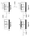
- Figures 1A up to 1Dillustrate schematic views of a Cu structure onto which an improved CuSi x N z and/or CuGe y N z capping layer is formed according to preferred embodiments of the present invention.
- Figure 2illustrates a flow chart illustrating a preferred embodiment of the method to provide a CuSi x N z and/or CuGe y N z (dual) capping layer with improved and stable sheet resistance.
- FIG. 3illustrates the sheet resistance (Rs) evolution of Plasma Vapour Deposited copper (PVD-Cu) having a CuGeN capping layer on top using state of the art processing (std) and using the method according to preferred embodiments of the invention compared to PVD-Cu without a CuGeN capping layer.
- FIG 4illustrates the sheet resistance (Rs) evolution of Electrochemically deposited copper (ECP-Cu) having a CuGeN capping layer on top using state of the art processing (std) and using the method according to preferred embodiments of the invention compared to ECP-Cu without a CuGeN capping layer.
- ECP-Cuhaving chemical Mechanical processing to planarize the ECP-Cu
- the Rs of ECP-Cuis much lower and has a different starting Rs value compared to PVD-Cu
- the present inventionrelates to a novel method to provide a capping layer onto a copper interconnect structure thereby avoiding plasma damage and resulting in improved capping layer characteristics such as lower sheet resistance (Rs) increase and good barrier performance (no or negligible Cu out-diffusion).
- Thisis achieved by introducing a pre annealing step (annealing the copper interconnect structure) prior to the step of providing the capping layer and/or by the step of introducing NH 3 to the GeH 4 /SiH 4 comprising gas.
- a pre annealing stepannealing the copper interconnect structure
- NH 3 to the GeH 4 /SiH 4 comprising gasBy introducing NH 3 in the GeH 4 /SiH 4 comprising gas the nitridation of the copper silicide and/or copper germanide occurs during the formation step (of the capping layer).
- the present inventionfurther relates to a novel composition and/or a novel stack of capping layers to be used on top of a copper interconnect structure such as a trench and a via in a (dual) damascene type structure.
- the novel composition and/or stacking of layerssolves the problem of bad adhesion and bad barrier performance.
- novel composition and/or a novel stack of capping layersgives improved electromigration performance and improved (lower) resistivity.
- the novel composition of the capping layercorresponds to a CuSi x Ge y N z layer whereas the stack of capping layers (also referred to as “dual” capping layer) corresponds to a CuSi x N z and a CuGe y N z layer on top of each other.
- One aspect of the present inventionrelates to a method to selectively provide a capping layer comprising Cu, Si and/or Ge onto (on top of) an embedded copper conductive structure, the method comprising at least the steps of:
- the pre-annealing stepis performed in a temperature range of 250°C up to 450°C.
- the pre-annealing stepis performed at 400°C for 30 minutes.
- the GeH 4 and/or SiH 4 comprising ambientfurther comprises (besides NH 3 ) an inert gas such as N 2 .
- the step of selective growth of at least one capping layeris such that the Cu structure is exposed to an ambient comprising GeH 4 and a CuGe y N z capping layer is deposited.
- the step of selective growth of at least one capping layeris such that the Cu structure is exposed to an ambient comprising SiH 4 and a CuSi x N z capping layer is deposited.
- the step of selective growth of at least one capping layeris such that the Cu structure is exposed to an ambient comprising GeH 4 and/or SiH 4 and a CuSi x Ge y N z capping layer is deposited.
- the step of selective growth of at least one capping layeris repeated twice such that a stacking of two capping layers is achieved of a CuSi x N z and a CuGe y N z capping layer.
- an additional thermal anneal stepis performed after the step of forming at least one capping layer.
- an additional thermal anneal stepis performed after the step of performing a NH 3 plasma treatment.
- an additional thermal anneal stepis performed after the step of depositing a dielectric barrier.
- a semiconductor devicecomprising:
- the self-aligned capping layer in a semiconductor device according to the present inventionis a stacking of two capping layers made of a CuSi x N z and a CuGe y N z capping layer.
- the self-aligned capping layer in a semiconductor device according to the present inventionhas a thickness in the range of 3nm up to 20nm.
- the semiconductor device according to the present inventioncomprises a dielectric barrier covering (on top of) the self-aligned capping layer and insulating layer.
- a methodfor depositing at least one a copper germanide nitride (CuGe y N z ) and/or copper silicide nitride (CuSi x N z ) onto (on top of) a copper conductive structure.
- CuGe y N zcopper germanide nitride
- CuSi x N zcopper silicide nitride
- Figures 1A up to 1Dillustrate schematic views of a Cu structure onto which an improved CuSi x N z and/or CuGe y N z capping layer is formed according to preferred embodiments of the present invention.
- Figure 2illustrates a flow chart illustrating a preferred embodiment of the method to provide a CuSi x N z and/or CuGe y N z (dual) capping layer with improved and stable sheet resistance.
- the method to selectively provide a capping layer comprising Cu, (and also) Si and/or Ge onto (on top of) an embedded copper conductive structurecomprises at least the steps of:
- the Cu structureis part of single or dual damascene interconnect structure (trench or via) .
- the Cu structureis embedded in a dielectric layer such as SiO 2 and other state of the art low-k dielectric material which are used to isolate interconnect structures.
- the dielectric layeris deposited on a semiconductor substrate (e.g. wafer) which further comprises active components.
- the capping layercomprises Cu, (and also) Si and/or Ge.
- the step of pre-annealing the Cu structureis performed to have additional Cu grain growth.
- the additional grain growth on a post Cu-CMP surface or in other words the additional anneal step to achieve grain growth (performed after chemical mechanical planarizing (CMP) the Cu-surface)effectively eliminates defects and grain boundaries which are fast Si and/or Ge diffusing paths.
- the present inventionsolves the problem of avoiding a Si and/or Ge diffusing path by performing a pre-anneal step (immediately or not) after the CMP step.
- This step of pre-annealingis preferably performed in temperature range of 250°C up to 450°C.
- a preferred pre-annealingis performed at 400°C for 30 minutes.
- the pre-annealing stepseemed to be mandatory for achieving low Rs of metal line.
- the pre-annealing stepmay be performed in the same chamber into which the deposition of the capping layer takes place, e.g. in a Chemical Vapour Deposition chamber.
- the pre-annealing stepmay be performed by a Rapid Thermal Anneal (RTA).
- RTARapid Thermal Anneal
- the step of pre-annealing the Cu structure before formation of the capping layeravoids Ge or Si impurity (diffusion) into the Cu structure from the capping layer or from the GeH 4 and SiH 4 gases during the formation of the capping layer.
- Ge or Si impurity in the Cu grain boundary or interface or Cu grain which will retard the Cu grain growth and increase Cu resistivitycan be effectively reduced.
- the Ge or Si impurity induced high sheet resistance (Rs)is hence improved.
- the step of selectively growing (or forming, or depositing) at least one capping layer onto the Cu structuremay be performed by exposing the copper structure to a GeH 4 (and/or SiH 4 ) comprising ambient.
- the temperature during the stepis preferably in the range of 200°C up to 400°C.
- the thickness of the capping layermay be in the range of 3nm up to 20nm.
- NH 3is added to the GeH 4 (and/or SiH 4 ) comprising ambient.
- the ambientcan further comprise inert compounds such as nitrogen gas (N 2 ).
- inert compoundssuch as nitrogen gas (N 2 ).
- the step of growing (or forming, or depositing) a capping layeris performed by exposing the pre-annealed Cu structure to a SiH 4 ambient to achieve at least a copper silicide capping layer.
- NH 3 during growth (or formation, or deposition) of the capping layerleads to at least a partly nitrided copper silicide layer or CuSi x N z layer.
- a CuSi x N z layeris selectively formed on top of the Cu structure or in other words a self aligned CuSi x N z layer is formed.
- the step of growing (or forming, or depositing) a capping layeris performed by exposing the pre-annealed Cu structure to a GeH 4 ambient to achieve at least a copper germanide capping layer.
- NH 3 during growth (or formation, or deposition) of the capping layerleads to at least a partly nitrided copper germanide layer or CuGe y N z layer.
- a CuGe y N z layeris selectively formed on top of the Cu structure or in other words a self aligned CuGe y N z layer is formed.
- the step of growing (or forming, or depositing) at least one capping layeris such that a dual capping layer is formed made of two capping layers.
- the formation of a dual capping layeris performed by first exposing the pre-annealed Cu structure to a GeH 4 (or SiH 4 ) ambient to achieve at least a first copper germanide (or silicide) capping layer and then exposing the Cu structure to a SiH 4 (or GeH 4 ) ambient to achieve at least a second copper silicide (or germanide) capping layer.
- NH 3 during growth (or formation, or deposition) of the capping layersleads to at least a partly nitrided copper germanide (or silicide) layer or CuGe y N z (or CuSi x N z ) layer.
- a dual layer containing (or comprising or consisting of) a CuGe y N z layer and a CuSi x N z layeris selectively formed on top of the Cu structure or in other words a self aligned dual capping layer is formed.
- the at least one capping layercontains Si and Ge to achieve a combined capping layer according to the formula CuSi x Ge y N z being able to combine properties of both CuGe y N z and CuSi x N z layers.
- This step of selectively growing (or forming, or depositing) the combined CuSi x Ge y N z layeris performed by exposing the Cu surface to a GeH 4 and SiH 4 comprising ambient wherein NH 3 is added (optional).
- the Cu surfaceis exposed to a SiH 4 and GeH 4 comprising ambient.
- the Cu surfaceis exposed to a SiH 4 and GeH 4 comprising ambient wherein NH 3 is be added.
- NH 3during the formation of the capping layer is beneficial to avoid (reduce) Ge (and/or Si) penetration from the capping layer into the Cu structure.
- an additional thermal anneal stepmay be performed after the step of forming at least one capping layer.
- the nitrogen gas (NH 3 ) addition during the GeH 4 or SiH 4 thermal reaction with Cu during the CuGe y N z and CuSi x N z formationmay also reduce the mobile/free Ge and Si to penetrate into Cu structure and hence reduce Rs.
- the step of performing a NH 3 plasma treatment after growing (or forming, or depositing) the capping layeris performed to achieve a fully nitrided capping layer.
- an additional thermal anneal stepmay be performed after the step of performing a NH 3 plasma treatment to achieve a fully nitrided capping layer.
- the step of depositing a dielectric barrier on top of the at least one capping layermay comprise the deposition of a etch stop layer which has a dielectric constant of less than about 4.
- Suitable examples of such layersare silicon carbide (SiC), carbon-doped silicon nitride (SiCN), carbon-doped silicon oxide (SiCO), silicon nitride (SiN), carbon-based materials, as well as germanium carbide (GeC), carbon-doped germanium nitride (GeCN), carbon-doped germanium oxide (GeCO), germanium nitride (GeN), and combinations thereof.
- the preferred thickness of the dielectric barrier layeris between about 20nm and about 100nm.
- the dielectric barrier layercan also be formed "in situ" after the formation of the capping layer, for example, if GeH 4 and NH 3 gases co-exist in a plasma environment, germanium nitride will be formed as a blanket layer fully covering the corresponding wafer.
- an additional thermal anneal stepmay be performed after the step of depositing a dielectric barrier.
- the novel capping layer composition layer(combined layer CuSi x Ge y N z ) or the novel dual capping layer (CuSi x N z /CuGe y N z or CuGe y N z /CuSi x N z ) may combine the benefits of a CuSi x N z and a CuGe y N z layer.
- CuSi x N zis known to provide better barrier performance than CuGeyN z at Cu out-diffusion. So CuSi x N z as a capping layer can allow the use of thinner ESL (SiC, SiCN, SiCNO..) for lower effective-k value.
- Si in CuSi x N zwill diffuse faster than Ge in CuGe y N z into the Cu, more pronounced Rs increase for CuSi x N z than CuGe y N z when they are used as Cu capping layers.
- CuSi x N z and CuGe y N zcan provide good performance for lower Rs increase and anti Cu-out diffusion for lower effective-k.
- Figure 4illustrates the sheet resistance (Rs) evolution of electrochemically deposited copper (ECP-Cu) having a CuGe y N z capping layer on top using state of the art processing (std) and using the method according to preferred embodiments of the invention compared to ECP-Cu without a CuGeN capping layer.
- Example 1Formation of a CuSi x Ge y N z capping layer
- Suitable process parameters for depositing a CuSi x Ge y N z capping layer(after having performed a thermal (pre) annealing of the copper structure of e.g. 30 minutes at 400°C) in a Chemical Vapour Deposition (CVD) chamber are summarized below.
- pressure ⁇ 4 torr SiH 4 flow⁇ 100sccm GeH 4 flow ⁇ 10sccm N 2 flow ⁇ 20000sccm NH 3 flow ⁇ 1000sccm
- Suitable process parameters for depositing a dual capping layer (stack) CuSi x N z /CuGe y N zare similar to the condition mentioned above except the sequential use of GeH 4 or SiH 4 .
Landscapes
- Engineering & Computer Science (AREA)
- Physics & Mathematics (AREA)
- Condensed Matter Physics & Semiconductors (AREA)
- General Physics & Mathematics (AREA)
- Computer Hardware Design (AREA)
- Microelectronics & Electronic Packaging (AREA)
- Power Engineering (AREA)
- Manufacturing & Machinery (AREA)
- Plasma & Fusion (AREA)
- Internal Circuitry In Semiconductor Integrated Circuit Devices (AREA)
Description
- The present invention is related to the field of semiconductor processing. More specifically it is related to the field of (e.g. copper) damascene advanced interconnect applications for integrated circuit (IC) manufacturing
- The present invention is in particular related to the production process of copper interconnect structures in the Back End of Line stages of the production process.
- The present invention is further related to the deposition of a selective capping layer on copper interconnect structures to improve electro-migration (EM) resistance.
- A commonly used method for forming metal interconnect lines (trenches) and vias in a semiconductor device is known as "damascene". Generally, this method involves forming an opening in a dielectric layer, which separates the vertically spaced metallization layers. The opening is typically formed using conventional lithographic and etching techniques. After the formation, the opening is filled with copper or copper alloys to form a via or a trench. Excess metal material on the surface of the dielectric layer is then removed by chemical mechanical polish (CMP). The remaining copper or copper alloy forms vias and/or metal interconnect lines.
- Copper is typically used in the damascene process because of its lower resistivity. However, copper suffers from electro-migration (EM) and stress-migration (SM) reliability issues, particularly as geometries continue to shrink and current densities continue to increase. Therefore, barrier layers are typically formed to prevent copper from diffusing into neighbouring low-k dielectric materials. Recently, copper silicide nitride layers are increasingly used as barrier layers.
- In order to maintain narrow lines reliability performances, Cu/low k interconnect architectures including Self Aligned Barriers on top of Cu lines are widely investigated as an effective solution for the 45 nm generation and beyond. Indeed, electromigration is a major concern for narrow Cu lines coated by dielectric barriers such as SiCN, SiCH and SiCO. Alternative approaches with self aligned barriers are already implemented to improve interconnect performance.
- Gosset et al. (Self Aligned Barrier Approach: Overview on Process, Module Integration and Interconnect Performance Improvement Challenges, International Interconnect Technology Conference, 2006 IEEE) describes a self aligned barrier (capping layer) integration, using either a Cu line surface treatment or a selective deposition process on top of the Cu lines. A CuSiN capping layer has been developed for its direct compatibility with existing PE-CVD processes and tools. It consists in a three steps process wherein first the native Cu oxide is removed using reducing plasmas (e.g. H2-based plasmas). In a second step, Cu silicidation, copper is enriched with Si atoms using Si-based precursor decomposition (CVD) such as silane or tri-methyl silane. Finally, a NH3 plasma is performed to achieve the CuSiN self aligned barrier.
- Usami et al. (Highly Reliable Interface of Self-aligned CuSiN process with Low-k SiC barrier dielectric (k=3.5) for 65nm node and beyond, International Interconnect Technology Conference, 2006 IEEE) describes also the deposition of a CuSiN self aligned barrier. In a first step, after planarizing the wafer (Cu-CMP), a reducing plasma was applied to remove surface copper oxide. In a second step, SiH4 gas was exposed on copper surface to diffuse silicon atoms into the copper film. In a third step, post nitrogen containing plasma was applied to scavenge the excess silicon atom and generate Si-N bonds for silicon pinning. Finally, the low k SiC barrier film is deposited on the copper lines. SiC was deposited in a conventional PE-CVD reactor using a more complex organic methyl silane source than the standard precursor used for SiCN (k=4.9) deposition.
- In
US 6,821,890 a process is disclosed to provide an intervening capping layer of copper germanide, germanide oxide, germanium nitride or combinations thereof to improve adhesion of poorly adhering material onto the copper surface. - The conventional formation process of barrier layers such as copper silicide still suffers from drawbacks. Since copper silicide is relatively unstable, silicon may still break from copper silicide and diffuse into low-k dielectric layer. Therefore, it is preferred that copper silicide layer is fully nitrated to form copper silicide nitride, which is more stable. This requires long NH3 plasma treatment and/or high power. However, plasma treatments have the side effect of incurring damage to low-k dielectric layer.
- [0009a]Chhun et al. (Microelectronic Engineering 82 (2005) 587-593) describes a silicidation mechanism and demonstrates the crucial role of a nitridation step in terms of barrier stability under electrical stress. CuSiN efficiency against Cu diffusion is also evidenced.
- [0009b]Chhun et al. (Microelectronic Engineering 83 (2006) 2094-2100) proposes a technique based on the modification of a Cu surface. It consists first in removing native Cu oxide, then, enriching the Cu surface with Si atoms followed by a nitridation step to complete the so called CuSiN self-aligned barrier.
- [0009c]
US 6,358,840 relates generally to fabrication of integrated circuits, and more particularly, to forming a recess in an interconnect, such as copper interconnect for example, by partially filling an interconnect opening, and to filling the recess with an alloy to form an additional encapsulating material during a thermal anneal on top of the interconnect for preventing material comprising the interconnect from laterally drifting into surrounding insulating material. - [0009d]
US 2007/0075428 discloses an integrated circuit device comprising a partially embedded and encapsulated damascene structure and a method for forming the same to improve adhesion to an overlying dielectric layer, the integrated circuit device including a conductive material partially embedded in an opening formed in a dielectric layer; wherein said conductive material is encapsulated with a first barrier layer comprising sidewall and bottom portions and a second barrier layer covering a top portion. - The documents
US 2002/0155702 andUS 2003/0224599 disclose methods of forming a CuSiN cap on Cu interconnects by exposure to an ambient containing SiH4, N2 and NH3. - The use of copper germanide as a capping layer has the advantage of being more stable and having a lower resistivity. However, copper germanide (and nitrided copper germanide) suffers from worse electromigration performance compared to a (nitrided) copper silicide capping layer.
- The conflicting requirements and needs for a suitable capping layer requires the need for a new capping layer composition as well as an improved method to provide a suitable capping layer which avoids e.g. damage to the surrounding dielectric material(s).
- A novel capping composition should be such that it combines good barrier performance (avoiding Cu out diffusing), low resistivity and stability of the capping layer with acceptable (low) sheet resistance increase.
- The present invention provides a method for obtaining at least one selective capping layer on Cu interconnect structures whereby the capping layer has improved electro-migration (EM) resistance and in combination therewith good barrier performance and acceptable and stable metal sheet resistance (Rs).
- The present invention therefore provides an improved fabrication process (of a capping layer) as well as a novel capping layer composition.
- One aspect according to the present invention provides a method for, preferably selectively, forming (or providing, or depositing) a capping layer comprising Cu, N, and also Si and/or Ge onto (or on top of) a copper conductive structure, said method comprising the sequential steps of:
- forming (or providing, or depositing), at a temperature range between 200°C up to 400°C, at least one capping layer, preferably selectively, onto said copper conductive structure by exposing said structure to a GeH4 and/or a SiH4 comprising ambient,
- performing a NH3 plasma treatment thereby forming an at least partly nitrided capping layer,
- forming (or providing, or depositing) a dielectric barrier layer onto (on top of) said at least partly nitrided capping layer,
- prior to said step of forming said at least one capping layer a pre-annealing step of said copper conductive structure is performed at a temperature range between 250°C up to 450°C, characterized in that:
- NH3 gas is added to said GeH4 and/on SiH4 comprising ambient thereby forming an at least partly nitrided capping layer
- Preferably, the wording "selectively forming a layer" as used in the present invention means "forming said layer onto (or on top of)" the Cu structure.
- Preferably, the copper conductive structure is meant to form vias and/or metal interconnect lines in a semiconductor device according to the present invention.
- Preferably, the wording "at least partly nitrided capping layer" as used in the present invention means that the capping layer is at least partly saturated with nitrogen.
- Preferably, in a method according to the invention, said pre-annealing step of said copper conductive structure is performed (immediately or not) after chemical mechanical planarizing (CMP) the Cu-surface.
- Preferably, in a method according to the invention, said pre-annealing step of said copper conductive structure is performed at a temperature range between 300°C up to 450°C, more preferably between 350°C up to 450°C, and even more preferably between 350°C up to 400°C.
- Preferably, in a method according to the invention, said pre-annealing step of said copper conductive structure is performed for at least 15 minutes, preferably for at least 30 minutes.
- More preferably, said pre-annealing step of said copper conductive structure is performed at (about) 400°C.
- Preferably, said (additional) pre-annealing step differs significantly from the (pre)heating performed in the CVD reactor prior to deposition (prior art method).
- More preferably, the amount of energy applied during said (additional) pre-annealing step differs from the amount of energy applied during said (pre)heating performed in the CVD reactor prior to deposition (prior art method) .
- More preferably, the time of heating of said (additional) pre-annealing step differs from the time of heating of said (pre)heating performed in the CVD reactor prior to deposition (prior art method).
- Preferably, said (additional) pre-annealing step of said copper conductive structure is performed at a temperature to have (additional) Cu grain growth.
- More preferably, said ambient comprises, or preferably consists of, GeH4 mixed with NH3 gas for forming an at least partly nitrided copper germanide (CuGeyNz) capping layer.
- Said CuGeyNz capping layer is a material comprising, or preferably consisting of, copper, germanium, and nitrogen.
- In said CuGeyNz capping layer, y and z are different form zero.
- Said CuGeyNz capping layer is a material comprising equivalent benefits from germanium and nitrogen.
- Said CuGeyNz capping layer is a material comprising at least 25% mole fraction of each of germanium and nitrogen.
- Said CuGeyNz capping layer is referred to as, preferably at least partly, nitrided copper germanide.
- Said CuGeyNz capping layer is also referred to as copper germanide nitride.
- Preferably, in a method according to the invention, said ambient comprises, or preferably consists of, SiH4 mixed with NH3 gas for forming an at least partly nitrided copper silicide (CuSixNz) capping layer.
- Said CuSixNz capping layer is a material comprising, or preferably consisting of, copper, silicon, and nitrogen.
- In said CuSixNz capping layer, x and z are different form zero.
- Said CuSixNz capping layer is a material comprising equivalent benefits from silicon and nitrogen.
- Said CuSixNz capping layer is a material comprising at least 25% mole fraction of each of silicon and nitrogen.
- Said CuSixNz capping layer is referred to as, preferably at least partly, nitrided copper silicide.
- Said CuSixNz capping layer is also referred to as copper silicide nitride.
- Preferably, in a method according to the invention, said ambient comprises, or preferably consists of, GeH4 and SiH4 mixed with NH3 gas for forming an at least partly nitrided copper silicon germanide (CuSixGeyNz) capping layer.
- Said CuSixGeyNz capping layer is a material comprising, or preferably consisting of, copper, silicon, germanium, and nitrogen.
- In said CuSixGeyNz capping layer, x, y, and z are different form zero.
- Said CuSixGeyNz capping layer is a material comprising equivalent benefits from silicon, germanium, and nitrogen.
- Said CuSixGeyNz capping layer is a material comprising at least 25% mole fraction of each of silicon, germanium, and nitrogen.
- Said CuSixGeyNz capping layer is referred to as, preferably at least partly, nitrided copper silicon germanide.
- Said CuSixGeyNz capping layer is also referred to as copper silicon germanide nitride.
- Said CuSixGeyNz capping layer is referred to as a combined capping layer.
- Preferably, in a method according to the invention, after said step of forming said at least one capping layer or after said step of performing said NH3 plasma treatment, the step of forming said at least one capping layer is repeated for forming a stack comprising, or preferably consisting of, two capping layers, one comprising a partly nitrided copper germanide (CuGeyNz) capping layer and another one comprising a partly nitrided copper silicide (CuSixNz) capping layer.
- Preferably, said step of forming said at least one capping layer is repeated for improving the quality of said capping layer(s).
- Preferably, repeating said step of forming said at least one capping layer for forming a stack comprising, or preferably consisting of, two capping layers is performed, preferably subsequently, after performing said (first) step of forming said at least one capping layer.
- Preferably, repeating said step of forming said at least one capping layer for forming a stack comprising, or preferably consisting of, two capping layers is performed, preferably subsequently, after performing said step of performing said NH3 plasma treatment.
- Said stack comprising, or preferably consisting of, two capping layers, one comprising a partly nitrided copper germanide (CuGeyNz) capping layer and another one comprising a partly nitrided copper silicide (CuSixNz) capping layer, is referred to as a dual capping layer.
- Preferably, in a method according to the invention, said GeH4 and/or SiH4 comprising ambient comprises (besides NH3) an inert gas such as nitrogen (N2).
- Preferably, in a method according to the invention, a thermal anneal step is performed after said step of forming said capping layer(s), after said step of forming said at least partly nitrided capping layer(s), and/or after said step of forming said dielectric barrier layer.
- Preferably, after the step of forming said at least one capping layer a thermal anneal step is performed.
- Preferably, after the step of performing a NH3 plasma treatment a thermal anneal step is performed.
- Preferably, after the step of forming a dielectric barrier layer a thermal anneal step is performed.
- Preferably, in a method according to the invention, said step of pre-annealing said copper structure and said step of, preferably selectively, forming said capping layer(s) and/or said partly nitrided capping layer(s) are performed in the same chamber.
- Preferably, in a method according to the invention, said step of pre-annealing said copper structure and said step of, preferably selectively, forming said capping layer(s) and/or said partly nitrided capping layer(s) are performed in another chamber.
- The method of the present invention provides a, preferably self-aligned, at least partly nitrided copper silicon germanide (CuSixGeyNz) capping layer on top of (or onto) an embedded copper conductive structure obtainable by a method according to the invention.
- Preferably, a "self-aligned layer" as used in the present invention means "a layer selectively formed onto (or on top of)" the Cu structure.
- The self-aligned capping layer is formed only in those areas in which the copper structure is in direct contact with silicon and/or germanium.
- Preferably, said CuSixGeyNz layer is a material for use as a capping layer.
- Preferably, the thickness of said at least partly nitrided copper silicon germanide (CuSixGeyNz) capping layer is in the range of 3nm up to 20nm.
- Another aspect of the present invention provides a semiconductor device comprising, or preferably consisting of:
- a semiconductor substrate,
- an insulating layer over the semiconductor substrate said insulating layer having an embedded copper conductive structure,
- a, preferably self-aligned, capping layer comprising, or preferably consisting of, a stack of two capping layers comprising a partly nitrided copper silicide (CuSixNz) capping layer and a partly nitrided copper germanide (CuGeyNz) capping layer.
- Preferably, the thickness of said, preferably self-aligned, capping layer(s) is in the range of 3nm up to 20nm.
- Preferably, in an embodiment of the present invention, said semiconductor device comprises a dielectric barrier layer covering said, preferably self-aligned, capping layer(s) and said insulating layer.
- It is an advantage of certain embodiments of the present invention that bad adhesion and bad barrier performance are avoided.
- It is an advantage of certain embodiments of the present invention that a Si and/or a Ge diffusion (impurity) path into the copper structure is/are avoided.
- It is an advantage of certain embodiments of the present invention that the Ge and/or Si impurity induced high sheet resistance (Rs) of the copper structure is improved (or reduced).
- It is an advantage of certain embodiments of the present invention that the novel combined capping layer (CuSixGeyNz) or the novel dual capping layer (CuSixNz /CuGeyNz or CuGeyNz/CuSixNz) may combine the benefits of a CuSixNz layer and a CuGeyNz layer.
- All drawings are intended to illustrate some aspects and embodiments of the present invention. Not all alternatives and options are shown and therefore the invention is not limited to the content of the given drawings.
Figures 1A up to 1D illustrate schematic views of a Cu structure onto which an improved CuSixNz and/or CuGeyNz capping layer is formed according to preferred embodiments of the present invention.Figure 2 illustrates a flow chart illustrating a preferred embodiment of the method to provide a CuSixNz and/or CuGeyNz (dual) capping layer with improved and stable sheet resistance.Figure 3 illustrates the sheet resistance (Rs) evolution of Plasma Vapour Deposited copper (PVD-Cu) having a CuGeN capping layer on top using state of the art processing (std) and using the method according to preferred embodiments of the invention compared to PVD-Cu without a CuGeN capping layer.Figure 4 illustrates the sheet resistance (Rs) evolution of Electrochemically deposited copper (ECP-Cu) having a CuGeN capping layer on top using state of the art processing (std) and using the method according to preferred embodiments of the invention compared to ECP-Cu without a CuGeN capping layer. Compared to PVD-Cu, ECP-Cu (having chemical Mechanical processing to planarize the ECP-Cu) has a much thicker initial Cu thickness. For that reason the Rs of ECP-Cu is much lower and has a different starting Rs value compared to PVD-Cu)- The present invention relates to a novel method to provide a capping layer onto a copper interconnect structure thereby avoiding plasma damage and resulting in improved capping layer characteristics such as lower sheet resistance (Rs) increase and good barrier performance (no or negligible Cu out-diffusion). This is achieved by introducing a pre annealing step (annealing the copper interconnect structure) prior to the step of providing the capping layer and/or by the step of introducing NH3 to the GeH4/SiH4 comprising gas. By introducing NH3 in the GeH4/SiH4 comprising gas the nitridation of the copper silicide and/or copper germanide occurs during the formation step (of the capping layer).
- The present invention further relates to a novel composition and/or a novel stack of capping layers to be used on top of a copper interconnect structure such as a trench and a via in a (dual) damascene type structure.
- The novel composition and/or stacking of layers solves the problem of bad adhesion and bad barrier performance.
- Furthermore the novel composition and/or a novel stack of capping layers gives improved electromigration performance and improved (lower) resistivity.
- The novel composition of the capping layer (also referred to as "combined" capping layer) corresponds to a CuSixGeyNz layer whereas the stack of capping layers (also referred to as "dual" capping layer) corresponds to a CuSixNz and a CuGeyNz layer on top of each other.
- One aspect of the present invention relates to a method to selectively provide a capping layer comprising Cu, Si and/or Ge onto (on top of) an embedded copper conductive structure, the method comprising at least the steps of:
- Pre-annealing the Cu structure,
- Selective growth of at least one capping layer onto the Cu structure by exposing the structure to a GeH4 and/or SiH4 comprising ambient with additional NH3 gas,
- NH3 plasma treatment,
- Dielectric barrier deposition.
- Preferably, in a method according to the invention, the pre-annealing step is performed in a temperature range of 250°C up to 450°C.
- More preferably, the pre-annealing step is performed at 400°C for 30 minutes.
- Preferably, in a method according to the invention, the GeH4 and/or SiH4 comprising ambient further comprises (besides NH3) an inert gas such as N2.
- Preferably, in a method according to the invention, the step of selective growth of at least one capping layer is such that the Cu structure is exposed to an ambient comprising GeH4 and a CuGeyNz capping layer is deposited.
- Preferably, in a method according to the invention, the step of selective growth of at least one capping layer is such that the Cu structure is exposed to an ambient comprising SiH4 and a CuSixNz capping layer is deposited.
- Preferably, in a method according to the invention, the step of selective growth of at least one capping layer is such that the Cu structure is exposed to an ambient comprising GeH4 and/or SiH4 and a CuSixGeyNz capping layer is deposited.
- Preferably, the step of selective growth of at least one capping layer is repeated twice such that a stacking of two capping layers is achieved of a CuSixNz and a CuGeyNz capping layer.
- Preferably, in a method according to the invention, an additional thermal anneal step is performed after the step of forming at least one capping layer.
- Preferably, in a method according to the invention, an additional thermal anneal step is performed after the step of performing a NH3 plasma treatment.
- Preferably, in a method according to the invention, an additional thermal anneal step is performed after the step of depositing a dielectric barrier.
- According to a second aspect of the present invention, a semiconductor device is disclosed, comprising:
- A semiconductor substrate,
- An insulating layer over the semiconductor substrate said insulating layer having an embedded copper conductive structure,
- A self-aligned copper silicide (or silicon) germanide nitride (CuSixGeyNz) capping layer on top of the conductive structure.
- Preferably, the self-aligned capping layer in a semiconductor device according to the present invention is a stacking of two capping layers made of a CuSixNz and a CuGeyNz capping layer.
- Preferably, the self-aligned capping layer in a semiconductor device according to the present invention has a thickness in the range of 3nm up to 20nm.
- More preferably, the semiconductor device according to the present invention comprises a dielectric barrier covering (on top of) the self-aligned capping layer and insulating layer.
- In a first aspect of the invention, a method is provided for depositing at least one a copper germanide nitride (CuGeyNz) and/or copper silicide nitride (CuSixNz) onto (on top of) a copper conductive structure.
Figures 1A up to 1D illustrate schematic views of a Cu structure onto which an improved CuSixNz and/or CuGeyNz capping layer is formed according to preferred embodiments of the present invention.Figure 2 illustrates a flow chart illustrating a preferred embodiment of the method to provide a CuSixNz and/or CuGeyNz (dual) capping layer with improved and stable sheet resistance.- According to preferred embodiments, the method to selectively provide a capping layer comprising Cu, (and also) Si and/or Ge onto (on top of) an embedded copper conductive structure comprises at least the steps of:
- Pre-annealing the Cu structure
- Selective growth (or formation, or deposition) of at least one capping layer onto the Cu structure by exposing the structure to a GeH4 and/or SiH4 comprising ambient with an additional NH3 source gas
- NH3 plasma treatment
- Dielectric barrier deposition
- According to preferred embodiments the Cu structure is part of single or dual damascene interconnect structure (trench or via) .
- The Cu structure is embedded in a dielectric layer such as SiO2 and other state of the art low-k dielectric material which are used to isolate interconnect structures.
- The dielectric layer is deposited on a semiconductor substrate (e.g. wafer) which further comprises active components.
- According to preferred embodiments the capping layer comprises Cu, (and also) Si and/or Ge.
- According to preferred embodiments the step of pre-annealing the Cu structure is performed to have additional Cu grain growth.
- The additional grain growth on a post Cu-CMP surface or in other words the additional anneal step to achieve grain growth (performed after chemical mechanical planarizing (CMP) the Cu-surface) effectively eliminates defects and grain boundaries which are fast Si and/or Ge diffusing paths.
- The present invention solves the problem of avoiding a Si and/or Ge diffusing path by performing a pre-anneal step (immediately or not) after the CMP step.
- This step of pre-annealing is preferably performed in temperature range of 250°C up to 450°C.
- A preferred pre-annealing is performed at 400°C for 30 minutes.
- This thermal pre annealing leads to improved Rs of the copper structure.
- The pre-annealing step seemed to be mandatory for achieving low Rs of metal line.
- The pre-annealing step may be performed in the same chamber into which the deposition of the capping layer takes place, e.g. in a Chemical Vapour Deposition chamber.
- The pre-annealing step may be performed by a Rapid Thermal Anneal (RTA).
- The step of pre-annealing the Cu structure before formation of the capping layer avoids Ge or Si impurity (diffusion) into the Cu structure from the capping layer or from the GeH4 and SiH4 gases during the formation of the capping layer.
- Ge or Si impurity in the Cu grain boundary or interface or Cu grain which will retard the Cu grain growth and increase Cu resistivity can be effectively reduced.
- The Ge or Si impurity induced high sheet resistance (Rs) is hence improved.
- The step of selectively growing (or forming, or depositing) at least one capping layer onto the Cu structure may be performed by exposing the copper structure to a GeH4 (and/or SiH4) comprising ambient.
- The temperature during the step is preferably in the range of 200°C up to 400°C.
- The thickness of the capping layer may be in the range of 3nm up to 20nm.
- To achieve nitridation during the growth (or formation, or deposition) of the capping layer, NH3 is added to the GeH4 (and/or SiH4) comprising ambient.
- The ambient can further comprise inert compounds such as nitrogen gas (N2).
- According to embodiments of the invention, the step of growing (or forming, or depositing) a capping layer is performed by exposing the pre-annealed Cu structure to a SiH4 ambient to achieve at least a copper silicide capping layer.
- Further addition of NH3 during growth (or formation, or deposition) of the capping layer leads to at least a partly nitrided copper silicide layer or CuSixNz layer.
- A CuSixNz layer is selectively formed on top of the Cu structure or in other words a self aligned CuSixNz layer is formed.
- According to embodiments of the invention, the step of growing (or forming, or depositing) a capping layer is performed by exposing the pre-annealed Cu structure to a GeH4 ambient to achieve at least a copper germanide capping layer.
- Further addition of NH3 during growth (or formation, or deposition) of the capping layer leads to at least a partly nitrided copper germanide layer or CuGeyNz layer.
- A CuGeyNz layer is selectively formed on top of the Cu structure or in other words a self aligned CuGeyNz layer is formed.
- According to embodiments of the invention, the step of growing (or forming, or depositing) at least one capping layer is such that a dual capping layer is formed made of two capping layers.
- The formation of a dual capping layer is performed by first exposing the pre-annealed Cu structure to a GeH4 (or SiH4) ambient to achieve at least a first copper germanide (or silicide) capping layer and then exposing the Cu structure to a SiH4 (or GeH4) ambient to achieve at least a second copper silicide (or germanide) capping layer.
- Further addition of NH3 during growth (or formation, or deposition) of the capping layers leads to at least a partly nitrided copper germanide (or silicide) layer or CuGeyNz (or CuSixNz) layer.
- A dual layer containing (or comprising or consisting of) a CuGeyNz layer and a CuSixNz layer is selectively formed on top of the Cu structure or in other words a self aligned dual capping layer is formed.
- According to embodiments of the invention, the at least one capping layer contains Si and Ge to achieve a combined capping layer according to the formula CuSixGeyNz being able to combine properties of both CuGeyNz and CuSixNz layers.
- This step of selectively growing (or forming, or depositing) the combined CuSixGeyNz layer is performed by exposing the Cu surface to a GeH4 and SiH4 comprising ambient wherein NH3 is added (optional).
- In case selective growth (or formation, or deposition) of a self aligned CuSixGey layer is wanted, the Cu surface is exposed to a SiH4 and GeH4 comprising ambient.
- In case selective growth (or formation, or deposition) of a self aligned CuSixGeyNz layer is wanted, the Cu surface is exposed to a SiH4 and GeH4 comprising ambient wherein NH3 is be added.
- The addition of NH3 during the formation of the capping layer is beneficial to avoid (reduce) Ge (and/or Si) penetration from the capping layer into the Cu structure.
- According to embodiments of the invention, an additional thermal anneal step may be performed after the step of forming at least one capping layer.
- The nitrogen gas (NH3) addition during the GeH4 or SiH4 thermal reaction with Cu during the CuGeyNz and CuSixNz formation may also reduce the mobile/free Ge and Si to penetrate into Cu structure and hence reduce Rs.
- According to embodiments of the invention, the step of performing a NH3 plasma treatment after growing (or forming, or depositing) the capping layer is performed to achieve a fully nitrided capping layer.
- According to embodiments of the invention, an additional thermal anneal step may be performed after the step of performing a NH3 plasma treatment to achieve a fully nitrided capping layer.
- According to embodiments of the invention, the step of depositing a dielectric barrier on top of the at least one capping layer may comprise the deposition of a etch stop layer which has a dielectric constant of less than about 4.
- Suitable examples of such layers are silicon carbide (SiC), carbon-doped silicon nitride (SiCN), carbon-doped silicon oxide (SiCO), silicon nitride (SiN), carbon-based materials, as well as germanium carbide (GeC), carbon-doped germanium nitride (GeCN), carbon-doped germanium oxide (GeCO), germanium nitride (GeN), and combinations thereof.
- The preferred thickness of the dielectric barrier layer (etch stop layer) is between about 20nm and about 100nm.
- The dielectric barrier layer can also be formed "in situ" after the formation of the capping layer, for example, if GeH4 and NH3 gases co-exist in a plasma environment, germanium nitride will be formed as a blanket layer fully covering the corresponding wafer.
- According to embodiments of the invention, an additional thermal anneal step may be performed after the step of depositing a dielectric barrier.
- An advantageous feature of the embodiments of the present invention is that the novel capping layer composition layer (combined layer CuSixGeyNz) or the novel dual capping layer (CuSixNz /CuGeyNz or CuGeyNz/CuSixNz) may combine the benefits of a CuSixNz and a CuGeyNz layer.
- CuSixNz is known to provide better barrier performance than CuGeyNz at Cu out-diffusion. So CuSixNz as a capping layer can allow the use of thinner ESL (SiC, SiCN, SiCNO..) for lower effective-k value.
- On the other hand, Si in CuSixNz will diffuse faster than Ge in CuGeyNz into the Cu, more pronounced Rs increase for CuSixNz than CuGeyNz when they are used as Cu capping layers.
- Combining the benefits of CuSixNz and CuGeyNz: CuSixGeyNz or CuSixNz/CuGeyNz or CuGeyNz/CuSixNz stacks can provide good performance for lower Rs increase and anti Cu-out diffusion for lower effective-k.
Figure 4 illustrates the sheet resistance (Rs) evolution of electrochemically deposited copper (ECP-Cu) having a CuGeyNz capping layer on top using state of the art processing (std) and using the method according to preferred embodiments of the invention compared to ECP-Cu without a CuGeN capping layer.- Although the present invention and its advantages have been described in detail, it should be understood that various changes, substitutions and alterations can be made herein without departing from the scope of the invention as defined by the appended claims. Moreover, the scope of the present application is not intended to be limited to the particular embodiments of the process, machine, manufacture, and composition of matter, means, methods and steps described in the specification. As one of ordinary skill in the art will readily appreciate from the disclosure of the present invention, processes, machines, manufacture, compositions of matter, means, methods, or steps, presently existing or later to be developed, that perform substantially the same function or achieve substantially the same result as the corresponding embodiments described herein may be utilized according to the present invention. Accordingly, the appended claims are intended to include within their scope such processes, machines, manufacture, compositions of matter, means, methods, or steps.
- Suitable process parameters for depositing a CuSixGeyNz capping layer (after having performed a thermal (pre) annealing of the copper structure of e.g. 30 minutes at 400°C) in a Chemical Vapour Deposition (CVD) chamber are summarized below.
pressure ∼4 torr
SiH4 flow ∼ 100sccm
GeH4 flow∼10sccm
N2 flow ∼ 20000sccm
NH3 flow ∼ 1000sccm
Temperature 350°C for several seconds - The process parameters for the "in situ" post NH3 plasma treatment are:
- Plasma Power ∼500W
- NH3 flow ∼1000 sccm
- N2 flow ∼10000 sccm for ∼30 seconds at ∼350C
- Suitable process parameters for depositing a dual capping layer (stack) CuSixNz/CuGeyNz are similar to the condition mentioned above except the sequential use of GeH4 or SiH4.
Claims (16)
- A method for forming a capping layer (6) comprising Cu, N, and also Si and/or Ge onto a copper conductive structure (2), said method comprising the sequential steps of:- forming, at a temperature range between 200°C up to 400°C, at least one capping layer (4) onto said copper conductive structure (2) by exposing said structure to a GeH4 and/or a SiH4 comprising ambient (3),- performing a NH3 plasma treatment (5) thereby forming an at least partly nitrided capping layer (6),- forming a dielectric barrier layer (7) onto said at least partly nitrided capping layer (6), wherein- prior to said step of forming said at least one capping layer a pre-annealing step of said copper conductive structure is performed at a temperature range between 250°C up to 450°C, andcharacterized in that:- NH3 gas is added to said GeH4 and/or SiH4 comprising ambient, thereby forming an at least partly nitrided capping layer.
- The method according to claim 1, wherein the pre-annealing step is performed for at least 15 minutes, preferably for at least 30 minutes.
- The method according to claim 2, wherein the pre-annealing step is performed at 400°C.
- The method according to claim 1, wherein said ambient comprises GeH4 mixed with NH3 gas for forming an at least partly nitrided copper germanide capping layer.
- The method according to claim 1, wherein said ambient comprises SiH4 mixed with NH3 gas for forming an at least partly nitrided copper silicide capping layer.
- The method according to claim 1, wherein said ambient comprises GeH4 and SiH4 mixed with NH3 gas for forming an at least partly nitrided copper silicon germanide capping layer.
- The method according to any of claims 1 to 5, wherein after said step of forming said at least one capping layer or after said step of performing said NH3 plasma treatment, the step of forming said at least one capping layer is repeated for forming a stack comprising two capping layers, one comprising a partly nitrided copper germanide capping layer and another one comprising a partly nitrided copper silicide capping layer.
- The method according to any of preceding claims, wherein said GeH4 and/or SiH4 comprising ambient comprises an inert gas such as N2.
- The method according to any of preceding claims, wherein a thermal anneal step is performed after said step of forming said capping layer(s), after said step of forming said at least partly nitrided capping layer(s), and/or after said step of forming said dielectric barrier layer.
- The method according to any of preceding claims, wherein said step of pre-annealing said copper structure and said step of forming said capping layer(s) and/or said partly nitrided capping layer(s) are performed in the same chamber.
- The method according to any of preceding claims, wherein said step of pre-annealing said copper structure and said step of forming said capping layer(s) and/or said partly nitrided capping layer(s) are performed in another chamber.
- The method according to any of claims 6 or 8 to 11, wherein a self aligned at least partly nitrided copper silicon germanide capping layer (6) is formed on top of an embedded copper conductive structure (2).
- The method according to claim 12, wherein the thickness of said capping layer is in the range of 3nm up to 20nm.
- A semiconductor device comprising:- a semiconductor substrate,- an insulating layer over the semiconductor substrate said insulating layer (1) having an embedded copper conductive structure (2),characterised in that:- a self-aligned capping layer (6) comprising a stack of two capping layers comprising an at least partly nitrided copper silicide capping layer and an at least partly nitrided copper germanide capping layer.
- The semiconductor device according to claim 14, wherein the thickness of said self-aligned capping layer(s) is in the range of 3nm up to 20nm.
- The semiconductor device according to any of claims 14 to 15, wherein a dielectric barrier layer (7) is covering said self-aligned capping layer(s) and said insulating layer (1).
Priority Applications (3)
| Application Number | Priority Date | Filing Date | Title |
|---|---|---|---|
| US12/264,095US7858519B2 (en) | 2007-11-27 | 2008-11-03 | Integrated circuit and manufacturing method of copper germanide and copper silicide as copper capping layer |
| JP2008299124AJP5496493B2 (en) | 2007-11-27 | 2008-11-25 | Method for integrating and producing Cu germanide and Cu silicide as a Cu cap layer |
| CN200810176387.0ACN101515563B (en) | 2007-11-27 | 2008-11-25 | Manufacturing method of covering layer |
Applications Claiming Priority (1)
| Application Number | Priority Date | Filing Date | Title |
|---|---|---|---|
| US99058507P | 2007-11-27 | 2007-11-27 |
Publications (2)
| Publication Number | Publication Date |
|---|---|
| EP2065927A1 EP2065927A1 (en) | 2009-06-03 |
| EP2065927B1true EP2065927B1 (en) | 2013-10-02 |
Family
ID=39938379
Family Applications (1)
| Application Number | Title | Priority Date | Filing Date |
|---|---|---|---|
| EP08157374.3AActiveEP2065927B1 (en) | 2007-11-27 | 2008-05-30 | Integration and manufacturing method of Cu germanide and Cu silicide as Cu capping layer |
Country Status (4)
| Country | Link |
|---|---|
| US (1) | US7858519B2 (en) |
| EP (1) | EP2065927B1 (en) |
| JP (1) | JP5496493B2 (en) |
| CN (1) | CN101515563B (en) |
Families Citing this family (379)
| Publication number | Priority date | Publication date | Assignee | Title |
|---|---|---|---|---|
| WO2009055450A1 (en)* | 2007-10-25 | 2009-04-30 | Applied Materials, Inc. | Adhesion improvement of dielectric barrier to copper by the addition of thin interface layer |
| US20090269507A1 (en) | 2008-04-29 | 2009-10-29 | Sang-Ho Yu | Selective cobalt deposition on copper surfaces |
| US7737528B2 (en)* | 2008-06-03 | 2010-06-15 | International Business Machines Corporation | Structure and method of forming electrically blown metal fuses for integrated circuits |
| US10378106B2 (en) | 2008-11-14 | 2019-08-13 | Asm Ip Holding B.V. | Method of forming insulation film by modified PEALD |
| DE102008063417B4 (en)* | 2008-12-31 | 2016-08-11 | Globalfoundries Dresden Module One Limited Liability Company & Co. Kg | Local silicidation on contact hole bottoms in metallization systems of semiconductor devices |
| US9394608B2 (en) | 2009-04-06 | 2016-07-19 | Asm America, Inc. | Semiconductor processing reactor and components thereof |
| KR100937945B1 (en) | 2009-08-05 | 2010-01-21 | 주식회사 아토 | Method of manufacturing a semiconductor device |
| US8802201B2 (en) | 2009-08-14 | 2014-08-12 | Asm America, Inc. | Systems and methods for thin-film deposition of metal oxides using excited nitrogen-oxygen species |
| US8659155B2 (en)* | 2009-11-05 | 2014-02-25 | Taiwan Semiconductor Manufacturing Company, Ltd. | Mechanisms for forming copper pillar bumps |
| CN102263056A (en)* | 2010-05-26 | 2011-11-30 | 中芯国际集成电路制造(上海)有限公司 | Metal interconnection method |
| CN102468225B (en)* | 2010-11-18 | 2014-02-05 | 中芯国际集成电路制造(上海)有限公司 | Fuse structure and manufacturing method thereof |
| TWI458072B (en)* | 2010-12-16 | 2014-10-21 | Soitec Silicon On Insulator | Methods for directly bonding together semiconductor structures, and bonded semiconductor structures formed using such methods |
| US8778773B2 (en) | 2010-12-16 | 2014-07-15 | Soitec | Methods for directly bonding together semiconductor structures, and bonded semiconductor structures formed using such methods |
| US9312155B2 (en) | 2011-06-06 | 2016-04-12 | Asm Japan K.K. | High-throughput semiconductor-processing apparatus equipped with multiple dual-chamber modules |
| US10364496B2 (en) | 2011-06-27 | 2019-07-30 | Asm Ip Holding B.V. | Dual section module having shared and unshared mass flow controllers |
| US10854498B2 (en) | 2011-07-15 | 2020-12-01 | Asm Ip Holding B.V. | Wafer-supporting device and method for producing same |
| US20130023129A1 (en) | 2011-07-20 | 2013-01-24 | Asm America, Inc. | Pressure transmitter for a semiconductor processing environment |
| US9017481B1 (en) | 2011-10-28 | 2015-04-28 | Asm America, Inc. | Process feed management for semiconductor substrate processing |
| CN103531530A (en)* | 2012-07-05 | 2014-01-22 | 中芯国际集成电路制造(上海)有限公司 | Method for processing copper surface in interconnection |
| US9659799B2 (en) | 2012-08-28 | 2017-05-23 | Asm Ip Holding B.V. | Systems and methods for dynamic semiconductor process scheduling |
| US10714315B2 (en) | 2012-10-12 | 2020-07-14 | Asm Ip Holdings B.V. | Semiconductor reaction chamber showerhead |
| US8871639B2 (en) | 2013-01-04 | 2014-10-28 | Taiwan Semiconductor Manufacturing Company, Ltd. | Semiconductor devices and methods of manufacture thereof |
| US20160376700A1 (en) | 2013-02-01 | 2016-12-29 | Asm Ip Holding B.V. | System for treatment of deposition reactor |
| US10181443B2 (en) | 2013-02-04 | 2019-01-15 | Taiwan Semiconductor Manufacturing Company Limited | Support structure for barrier layer of semiconductor device |
| US8927420B2 (en) | 2013-02-04 | 2015-01-06 | Taiwan Semiconductor Manufacturing Company Limited | Mechanism of forming semiconductor device having support structure |
| US9484191B2 (en) | 2013-03-08 | 2016-11-01 | Asm Ip Holding B.V. | Pulsed remote plasma method and system |
| US9589770B2 (en) | 2013-03-08 | 2017-03-07 | Asm Ip Holding B.V. | Method and systems for in-situ formation of intermediate reactive species |
| US9988713B2 (en) | 2013-03-12 | 2018-06-05 | Arizona Board Of Regents On Behalf Of Arizona State University | Thin film devices and methods for preparing thin film devices |
| US9147605B2 (en) | 2013-06-14 | 2015-09-29 | Arizona Board Of Regents On Behalf Of Arizona State University | Thin film devices and low temperature process to make thin film devices |
| CN104299939B (en)* | 2013-07-16 | 2017-09-22 | 中芯国际集成电路制造(上海)有限公司 | The forming method of interconnection structure |
| JP6414899B2 (en)* | 2013-08-22 | 2018-10-31 | Necエナジーデバイス株式会社 | Negative electrode, method for producing the same, battery |
| US9240412B2 (en) | 2013-09-27 | 2016-01-19 | Asm Ip Holding B.V. | Semiconductor structure and device and methods of forming same using selective epitaxial process |
| KR102166898B1 (en)* | 2014-01-10 | 2020-10-19 | 삼성디스플레이 주식회사 | Thin film transistor array panel and method for manufacturing the same |
| US10683571B2 (en) | 2014-02-25 | 2020-06-16 | Asm Ip Holding B.V. | Gas supply manifold and method of supplying gases to chamber using same |
| US10167557B2 (en) | 2014-03-18 | 2019-01-01 | Asm Ip Holding B.V. | Gas distribution system, reactor including the system, and methods of using the same |
| US11015245B2 (en) | 2014-03-19 | 2021-05-25 | Asm Ip Holding B.V. | Gas-phase reactor and system having exhaust plenum and components thereof |
| US20160017487A1 (en)* | 2014-07-15 | 2016-01-21 | Applied Materials, Inc. | Integrated pre-clean and deposition of low-damage layers |
| US9559249B2 (en) | 2014-07-22 | 2017-01-31 | Arizona Board Of Regents | Microwave-annealed indium gallium zinc oxide films and methods of making the same |
| US10858737B2 (en) | 2014-07-28 | 2020-12-08 | Asm Ip Holding B.V. | Showerhead assembly and components thereof |
| US9890456B2 (en) | 2014-08-21 | 2018-02-13 | Asm Ip Holding B.V. | Method and system for in situ formation of gas-phase compounds |
| US9657845B2 (en) | 2014-10-07 | 2017-05-23 | Asm Ip Holding B.V. | Variable conductance gas distribution apparatus and method |
| US10941490B2 (en) | 2014-10-07 | 2021-03-09 | Asm Ip Holding B.V. | Multiple temperature range susceptor, assembly, reactor and system including the susceptor, and methods of using the same |
| JP2016111104A (en) | 2014-12-03 | 2016-06-20 | 株式会社Joled | Method of manufacturing thin-film semiconductor substrate |
| KR102263121B1 (en) | 2014-12-22 | 2021-06-09 | 에이에스엠 아이피 홀딩 비.브이. | Semiconductor device and manufacuring method thereof |
| US10529542B2 (en) | 2015-03-11 | 2020-01-07 | Asm Ip Holdings B.V. | Cross-flow reactor and method |
| US10276355B2 (en) | 2015-03-12 | 2019-04-30 | Asm Ip Holding B.V. | Multi-zone reactor, system including the reactor, and method of using the same |
| US10458018B2 (en) | 2015-06-26 | 2019-10-29 | Asm Ip Holding B.V. | Structures including metal carbide material, devices including the structures, and methods of forming same |
| US10600673B2 (en) | 2015-07-07 | 2020-03-24 | Asm Ip Holding B.V. | Magnetic susceptor to baseplate seal |
| US9960072B2 (en) | 2015-09-29 | 2018-05-01 | Asm Ip Holding B.V. | Variable adjustment for precise matching of multiple chamber cavity housings |
| US10211308B2 (en) | 2015-10-21 | 2019-02-19 | Asm Ip Holding B.V. | NbMC layers |
| US10322384B2 (en) | 2015-11-09 | 2019-06-18 | Asm Ip Holding B.V. | Counter flow mixer for process chamber |
| US11139308B2 (en) | 2015-12-29 | 2021-10-05 | Asm Ip Holding B.V. | Atomic layer deposition of III-V compounds to form V-NAND devices |
| CN114068724A (en) | 2016-01-29 | 2022-02-18 | 株式会社半导体能源研究所 | Semiconductor device and transistor |
| US10468251B2 (en) | 2016-02-19 | 2019-11-05 | Asm Ip Holding B.V. | Method for forming spacers using silicon nitride film for spacer-defined multiple patterning |
| US10529554B2 (en) | 2016-02-19 | 2020-01-07 | Asm Ip Holding B.V. | Method for forming silicon nitride film selectively on sidewalls or flat surfaces of trenches |
| US10501866B2 (en) | 2016-03-09 | 2019-12-10 | Asm Ip Holding B.V. | Gas distribution apparatus for improved film uniformity in an epitaxial system |
| US10343920B2 (en) | 2016-03-18 | 2019-07-09 | Asm Ip Holding B.V. | Aligned carbon nanotubes |
| US9892913B2 (en) | 2016-03-24 | 2018-02-13 | Asm Ip Holding B.V. | Radial and thickness control via biased multi-port injection settings |
| US10190213B2 (en) | 2016-04-21 | 2019-01-29 | Asm Ip Holding B.V. | Deposition of metal borides |
| US10865475B2 (en) | 2016-04-21 | 2020-12-15 | Asm Ip Holding B.V. | Deposition of metal borides and silicides |
| US10700276B2 (en)* | 2016-04-22 | 2020-06-30 | The Institute of Microelectronics of Chinese Academy of Sciences | Preparation method of Cu-based resistive random access memory, and memory |
| US10305035B2 (en)* | 2016-04-22 | 2019-05-28 | The Institute of Microelectronics of Chinese Academy of Sciences | Preparation method of Cu-based resistive random access memory |
| US10367080B2 (en) | 2016-05-02 | 2019-07-30 | Asm Ip Holding B.V. | Method of forming a germanium oxynitride film |
| US10032628B2 (en) | 2016-05-02 | 2018-07-24 | Asm Ip Holding B.V. | Source/drain performance through conformal solid state doping |
| KR102592471B1 (en) | 2016-05-17 | 2023-10-20 | 에이에스엠 아이피 홀딩 비.브이. | Method of forming metal interconnection and method of fabricating semiconductor device using the same |
| US11453943B2 (en) | 2016-05-25 | 2022-09-27 | Asm Ip Holding B.V. | Method for forming carbon-containing silicon/metal oxide or nitride film by ALD using silicon precursor and hydrocarbon precursor |
| US10388509B2 (en) | 2016-06-28 | 2019-08-20 | Asm Ip Holding B.V. | Formation of epitaxial layers via dislocation filtering |
| US10612137B2 (en) | 2016-07-08 | 2020-04-07 | Asm Ip Holdings B.V. | Organic reactants for atomic layer deposition |
| US9859151B1 (en) | 2016-07-08 | 2018-01-02 | Asm Ip Holding B.V. | Selective film deposition method to form air gaps |
| US10714385B2 (en) | 2016-07-19 | 2020-07-14 | Asm Ip Holding B.V. | Selective deposition of tungsten |
| US10916430B2 (en)* | 2016-07-25 | 2021-02-09 | Semiconductor Energy Laboratory Co., Ltd. | Semiconductor device and method for manufacturing the same |
| KR102354490B1 (en) | 2016-07-27 | 2022-01-21 | 에이에스엠 아이피 홀딩 비.브이. | Method of processing a substrate |
| KR102532607B1 (en) | 2016-07-28 | 2023-05-15 | 에이에스엠 아이피 홀딩 비.브이. | Substrate processing apparatus and method of operating the same |
| US10395919B2 (en) | 2016-07-28 | 2019-08-27 | Asm Ip Holding B.V. | Method and apparatus for filling a gap |
| US9887082B1 (en) | 2016-07-28 | 2018-02-06 | Asm Ip Holding B.V. | Method and apparatus for filling a gap |
| US9812320B1 (en) | 2016-07-28 | 2017-11-07 | Asm Ip Holding B.V. | Method and apparatus for filling a gap |
| KR102613349B1 (en) | 2016-08-25 | 2023-12-14 | 에이에스엠 아이피 홀딩 비.브이. | Exhaust apparatus and substrate processing apparatus and thin film fabricating method using the same |
| US10410943B2 (en) | 2016-10-13 | 2019-09-10 | Asm Ip Holding B.V. | Method for passivating a surface of a semiconductor and related systems |
| EP3310137B1 (en)* | 2016-10-14 | 2019-02-27 | ATOTECH Deutschland GmbH | Method for manufacturing a printed circuit board |
| US10643826B2 (en) | 2016-10-26 | 2020-05-05 | Asm Ip Holdings B.V. | Methods for thermally calibrating reaction chambers |
| US11532757B2 (en) | 2016-10-27 | 2022-12-20 | Asm Ip Holding B.V. | Deposition of charge trapping layers |
| US10229833B2 (en) | 2016-11-01 | 2019-03-12 | Asm Ip Holding B.V. | Methods for forming a transition metal nitride film on a substrate by atomic layer deposition and related semiconductor device structures |
| US10714350B2 (en) | 2016-11-01 | 2020-07-14 | ASM IP Holdings, B.V. | Methods for forming a transition metal niobium nitride film on a substrate by atomic layer deposition and related semiconductor device structures |
| US10435790B2 (en) | 2016-11-01 | 2019-10-08 | Asm Ip Holding B.V. | Method of subatmospheric plasma-enhanced ALD using capacitively coupled electrodes with narrow gap |
| US10643904B2 (en) | 2016-11-01 | 2020-05-05 | Asm Ip Holdings B.V. | Methods for forming a semiconductor device and related semiconductor device structures |
| US10134757B2 (en) | 2016-11-07 | 2018-11-20 | Asm Ip Holding B.V. | Method of processing a substrate and a device manufactured by using the method |
| KR102546317B1 (en) | 2016-11-15 | 2023-06-21 | 에이에스엠 아이피 홀딩 비.브이. | Gas supply unit and substrate processing apparatus including the same |
| US10340135B2 (en) | 2016-11-28 | 2019-07-02 | Asm Ip Holding B.V. | Method of topologically restricted plasma-enhanced cyclic deposition of silicon or metal nitride |
| KR102762543B1 (en) | 2016-12-14 | 2025-02-05 | 에이에스엠 아이피 홀딩 비.브이. | Substrate processing apparatus |
| US11581186B2 (en) | 2016-12-15 | 2023-02-14 | Asm Ip Holding B.V. | Sequential infiltration synthesis apparatus |
| US11447861B2 (en) | 2016-12-15 | 2022-09-20 | Asm Ip Holding B.V. | Sequential infiltration synthesis apparatus and a method of forming a patterned structure |
| KR102700194B1 (en) | 2016-12-19 | 2024-08-28 | 에이에스엠 아이피 홀딩 비.브이. | Substrate processing apparatus |
| US10269558B2 (en) | 2016-12-22 | 2019-04-23 | Asm Ip Holding B.V. | Method of forming a structure on a substrate |
| US10867788B2 (en) | 2016-12-28 | 2020-12-15 | Asm Ip Holding B.V. | Method of forming a structure on a substrate |
| US11390950B2 (en) | 2017-01-10 | 2022-07-19 | Asm Ip Holding B.V. | Reactor system and method to reduce residue buildup during a film deposition process |
| US10655221B2 (en) | 2017-02-09 | 2020-05-19 | Asm Ip Holding B.V. | Method for depositing oxide film by thermal ALD and PEALD |
| US10468261B2 (en) | 2017-02-15 | 2019-11-05 | Asm Ip Holding B.V. | Methods for forming a metallic film on a substrate by cyclical deposition and related semiconductor device structures |
| US10283353B2 (en) | 2017-03-29 | 2019-05-07 | Asm Ip Holding B.V. | Method of reforming insulating film deposited on substrate with recess pattern |
| US10529563B2 (en) | 2017-03-29 | 2020-01-07 | Asm Ip Holdings B.V. | Method for forming doped metal oxide films on a substrate by cyclical deposition and related semiconductor device structures |
| KR102457289B1 (en) | 2017-04-25 | 2022-10-21 | 에이에스엠 아이피 홀딩 비.브이. | Method for depositing a thin film and manufacturing a semiconductor device |
| US10446393B2 (en) | 2017-05-08 | 2019-10-15 | Asm Ip Holding B.V. | Methods for forming silicon-containing epitaxial layers and related semiconductor device structures |
| US10770286B2 (en) | 2017-05-08 | 2020-09-08 | Asm Ip Holdings B.V. | Methods for selectively forming a silicon nitride film on a substrate and related semiconductor device structures |
| US10892156B2 (en) | 2017-05-08 | 2021-01-12 | Asm Ip Holding B.V. | Methods for forming a silicon nitride film on a substrate and related semiconductor device structures |
| CN107256845A (en)* | 2017-05-25 | 2017-10-17 | 上海集成电路研发中心有限公司 | A kind of copper interconnection structure and its manufacture method |
| US10504742B2 (en) | 2017-05-31 | 2019-12-10 | Asm Ip Holding B.V. | Method of atomic layer etching using hydrogen plasma |
| US10886123B2 (en) | 2017-06-02 | 2021-01-05 | Asm Ip Holding B.V. | Methods for forming low temperature semiconductor layers and related semiconductor device structures |
| US12040200B2 (en) | 2017-06-20 | 2024-07-16 | Asm Ip Holding B.V. | Semiconductor processing apparatus and methods for calibrating a semiconductor processing apparatus |
| US11306395B2 (en) | 2017-06-28 | 2022-04-19 | Asm Ip Holding B.V. | Methods for depositing a transition metal nitride film on a substrate by atomic layer deposition and related deposition apparatus |
| US10685834B2 (en) | 2017-07-05 | 2020-06-16 | Asm Ip Holdings B.V. | Methods for forming a silicon germanium tin layer and related semiconductor device structures |
| KR20190009245A (en) | 2017-07-18 | 2019-01-28 | 에이에스엠 아이피 홀딩 비.브이. | Methods for forming a semiconductor device structure and related semiconductor device structures |
| US11018002B2 (en) | 2017-07-19 | 2021-05-25 | Asm Ip Holding B.V. | Method for selectively depositing a Group IV semiconductor and related semiconductor device structures |
| US10541333B2 (en) | 2017-07-19 | 2020-01-21 | Asm Ip Holding B.V. | Method for depositing a group IV semiconductor and related semiconductor device structures |
| US11374112B2 (en) | 2017-07-19 | 2022-06-28 | Asm Ip Holding B.V. | Method for depositing a group IV semiconductor and related semiconductor device structures |
| US10312055B2 (en) | 2017-07-26 | 2019-06-04 | Asm Ip Holding B.V. | Method of depositing film by PEALD using negative bias |
| US10590535B2 (en) | 2017-07-26 | 2020-03-17 | Asm Ip Holdings B.V. | Chemical treatment, deposition and/or infiltration apparatus and method for using the same |
| US10605530B2 (en) | 2017-07-26 | 2020-03-31 | Asm Ip Holding B.V. | Assembly of a liner and a flange for a vertical furnace as well as the liner and the vertical furnace |
| TWI815813B (en) | 2017-08-04 | 2023-09-21 | 荷蘭商Asm智慧財產控股公司 | Showerhead assembly for distributing a gas within a reaction chamber |
| US10692741B2 (en) | 2017-08-08 | 2020-06-23 | Asm Ip Holdings B.V. | Radiation shield |
| US10770336B2 (en) | 2017-08-08 | 2020-09-08 | Asm Ip Holding B.V. | Substrate lift mechanism and reactor including same |
| US10249524B2 (en) | 2017-08-09 | 2019-04-02 | Asm Ip Holding B.V. | Cassette holder assembly for a substrate cassette and holding member for use in such assembly |
| US11139191B2 (en) | 2017-08-09 | 2021-10-05 | Asm Ip Holding B.V. | Storage apparatus for storing cassettes for substrates and processing apparatus equipped therewith |
| US11769682B2 (en) | 2017-08-09 | 2023-09-26 | Asm Ip Holding B.V. | Storage apparatus for storing cassettes for substrates and processing apparatus equipped therewith |
| USD900036S1 (en) | 2017-08-24 | 2020-10-27 | Asm Ip Holding B.V. | Heater electrical connector and adapter |
| US11830730B2 (en) | 2017-08-29 | 2023-11-28 | Asm Ip Holding B.V. | Layer forming method and apparatus |
| KR102491945B1 (en) | 2017-08-30 | 2023-01-26 | 에이에스엠 아이피 홀딩 비.브이. | Substrate processing apparatus |
| US11295980B2 (en) | 2017-08-30 | 2022-04-05 | Asm Ip Holding B.V. | Methods for depositing a molybdenum metal film over a dielectric surface of a substrate by a cyclical deposition process and related semiconductor device structures |
| US11056344B2 (en) | 2017-08-30 | 2021-07-06 | Asm Ip Holding B.V. | Layer forming method |
| KR102401446B1 (en) | 2017-08-31 | 2022-05-24 | 에이에스엠 아이피 홀딩 비.브이. | Substrate processing apparatus |
| US10607895B2 (en) | 2017-09-18 | 2020-03-31 | Asm Ip Holdings B.V. | Method for forming a semiconductor device structure comprising a gate fill metal |
| KR102630301B1 (en) | 2017-09-21 | 2024-01-29 | 에이에스엠 아이피 홀딩 비.브이. | Method of sequential infiltration synthesis treatment of infiltrateable material and structures and devices formed using same |
| US10844484B2 (en) | 2017-09-22 | 2020-11-24 | Asm Ip Holding B.V. | Apparatus for dispensing a vapor phase reactant to a reaction chamber and related methods |
| US10658205B2 (en) | 2017-09-28 | 2020-05-19 | Asm Ip Holdings B.V. | Chemical dispensing apparatus and methods for dispensing a chemical to a reaction chamber |
| US10403504B2 (en) | 2017-10-05 | 2019-09-03 | Asm Ip Holding B.V. | Method for selectively depositing a metallic film on a substrate |
| US10319588B2 (en) | 2017-10-10 | 2019-06-11 | Asm Ip Holding B.V. | Method for depositing a metal chalcogenide on a substrate by cyclical deposition |
| US10923344B2 (en) | 2017-10-30 | 2021-02-16 | Asm Ip Holding B.V. | Methods for forming a semiconductor structure and related semiconductor structures |
| US10910262B2 (en) | 2017-11-16 | 2021-02-02 | Asm Ip Holding B.V. | Method of selectively depositing a capping layer structure on a semiconductor device structure |
| KR102443047B1 (en) | 2017-11-16 | 2022-09-14 | 에이에스엠 아이피 홀딩 비.브이. | Method of processing a substrate and a device manufactured by the same |
| US11022879B2 (en) | 2017-11-24 | 2021-06-01 | Asm Ip Holding B.V. | Method of forming an enhanced unexposed photoresist layer |
| WO2019103613A1 (en) | 2017-11-27 | 2019-05-31 | Asm Ip Holding B.V. | A storage device for storing wafer cassettes for use with a batch furnace |
| CN111344522B (en) | 2017-11-27 | 2022-04-12 | 阿斯莫Ip控股公司 | Including clean mini-environment device |
| US10290508B1 (en) | 2017-12-05 | 2019-05-14 | Asm Ip Holding B.V. | Method for forming vertical spacers for spacer-defined patterning |
| US10872771B2 (en) | 2018-01-16 | 2020-12-22 | Asm Ip Holding B. V. | Method for depositing a material film on a substrate within a reaction chamber by a cyclical deposition process and related device structures |
| TWI799494B (en) | 2018-01-19 | 2023-04-21 | 荷蘭商Asm 智慧財產控股公司 | Deposition method |
| KR102695659B1 (en) | 2018-01-19 | 2024-08-14 | 에이에스엠 아이피 홀딩 비.브이. | Method for depositing a gap filling layer by plasma assisted deposition |
| USD903477S1 (en) | 2018-01-24 | 2020-12-01 | Asm Ip Holdings B.V. | Metal clamp |
| US11018047B2 (en) | 2018-01-25 | 2021-05-25 | Asm Ip Holding B.V. | Hybrid lift pin |
| USD880437S1 (en) | 2018-02-01 | 2020-04-07 | Asm Ip Holding B.V. | Gas supply plate for semiconductor manufacturing apparatus |
| US10535516B2 (en) | 2018-02-01 | 2020-01-14 | Asm Ip Holdings B.V. | Method for depositing a semiconductor structure on a surface of a substrate and related semiconductor structures |
| US11081345B2 (en) | 2018-02-06 | 2021-08-03 | Asm Ip Holding B.V. | Method of post-deposition treatment for silicon oxide film |
| WO2019158960A1 (en) | 2018-02-14 | 2019-08-22 | Asm Ip Holding B.V. | A method for depositing a ruthenium-containing film on a substrate by a cyclical deposition process |
| US10896820B2 (en) | 2018-02-14 | 2021-01-19 | Asm Ip Holding B.V. | Method for depositing a ruthenium-containing film on a substrate by a cyclical deposition process |
| US10731249B2 (en) | 2018-02-15 | 2020-08-04 | Asm Ip Holding B.V. | Method of forming a transition metal containing film on a substrate by a cyclical deposition process, a method for supplying a transition metal halide compound to a reaction chamber, and related vapor deposition apparatus |
| US10658181B2 (en) | 2018-02-20 | 2020-05-19 | Asm Ip Holding B.V. | Method of spacer-defined direct patterning in semiconductor fabrication |
| KR102636427B1 (en) | 2018-02-20 | 2024-02-13 | 에이에스엠 아이피 홀딩 비.브이. | Substrate processing method and apparatus |
| US10975470B2 (en) | 2018-02-23 | 2021-04-13 | Asm Ip Holding B.V. | Apparatus for detecting or monitoring for a chemical precursor in a high temperature environment |
| US11473195B2 (en) | 2018-03-01 | 2022-10-18 | Asm Ip Holding B.V. | Semiconductor processing apparatus and a method for processing a substrate |
| US11629406B2 (en) | 2018-03-09 | 2023-04-18 | Asm Ip Holding B.V. | Semiconductor processing apparatus comprising one or more pyrometers for measuring a temperature of a substrate during transfer of the substrate |
| US11114283B2 (en) | 2018-03-16 | 2021-09-07 | Asm Ip Holding B.V. | Reactor, system including the reactor, and methods of manufacturing and using same |
| KR102646467B1 (en) | 2018-03-27 | 2024-03-11 | 에이에스엠 아이피 홀딩 비.브이. | Method of forming an electrode on a substrate and a semiconductor device structure including an electrode |
| US11088002B2 (en) | 2018-03-29 | 2021-08-10 | Asm Ip Holding B.V. | Substrate rack and a substrate processing system and method |
| US10510536B2 (en) | 2018-03-29 | 2019-12-17 | Asm Ip Holding B.V. | Method of depositing a co-doped polysilicon film on a surface of a substrate within a reaction chamber |
| US11230766B2 (en) | 2018-03-29 | 2022-01-25 | Asm Ip Holding B.V. | Substrate processing apparatus and method |
| KR102501472B1 (en) | 2018-03-30 | 2023-02-20 | 에이에스엠 아이피 홀딩 비.브이. | Substrate processing method |
| KR102600229B1 (en) | 2018-04-09 | 2023-11-10 | 에이에스엠 아이피 홀딩 비.브이. | Substrate supporting device, substrate processing apparatus including the same and substrate processing method |
| US12025484B2 (en) | 2018-05-08 | 2024-07-02 | Asm Ip Holding B.V. | Thin film forming method |
| TWI811348B (en) | 2018-05-08 | 2023-08-11 | 荷蘭商Asm 智慧財產控股公司 | Methods for depositing an oxide film on a substrate by a cyclical deposition process and related device structures |
| US12272527B2 (en) | 2018-05-09 | 2025-04-08 | Asm Ip Holding B.V. | Apparatus for use with hydrogen radicals and method of using same |
| KR20190129718A (en) | 2018-05-11 | 2019-11-20 | 에이에스엠 아이피 홀딩 비.브이. | Methods for forming a doped metal carbide film on a substrate and related semiconductor device structures |
| KR102596988B1 (en) | 2018-05-28 | 2023-10-31 | 에이에스엠 아이피 홀딩 비.브이. | Method of processing a substrate and a device manufactured by the same |
| US11718913B2 (en) | 2018-06-04 | 2023-08-08 | Asm Ip Holding B.V. | Gas distribution system and reactor system including same |
| TWI840362B (en) | 2018-06-04 | 2024-05-01 | 荷蘭商Asm Ip私人控股有限公司 | Wafer handling chamber with moisture reduction |
| US11286562B2 (en) | 2018-06-08 | 2022-03-29 | Asm Ip Holding B.V. | Gas-phase chemical reactor and method of using same |
| KR102568797B1 (en) | 2018-06-21 | 2023-08-21 | 에이에스엠 아이피 홀딩 비.브이. | Substrate processing system |
| US10797133B2 (en) | 2018-06-21 | 2020-10-06 | Asm Ip Holding B.V. | Method for depositing a phosphorus doped silicon arsenide film and related semiconductor device structures |
| KR102854019B1 (en) | 2018-06-27 | 2025-09-02 | 에이에스엠 아이피 홀딩 비.브이. | Periodic deposition method for forming a metal-containing material and films and structures comprising the metal-containing material |
| TWI873894B (en) | 2018-06-27 | 2025-02-21 | 荷蘭商Asm Ip私人控股有限公司 | Cyclic deposition methods for forming metal-containing material and films and structures including the metal-containing material |
| KR102686758B1 (en) | 2018-06-29 | 2024-07-18 | 에이에스엠 아이피 홀딩 비.브이. | Method for depositing a thin film and manufacturing a semiconductor device |
| US10612136B2 (en) | 2018-06-29 | 2020-04-07 | ASM IP Holding, B.V. | Temperature-controlled flange and reactor system including same |
| US10388513B1 (en) | 2018-07-03 | 2019-08-20 | Asm Ip Holding B.V. | Method for depositing silicon-free carbon-containing film as gap-fill layer by pulse plasma-assisted deposition |
| US10755922B2 (en) | 2018-07-03 | 2020-08-25 | Asm Ip Holding B.V. | Method for depositing silicon-free carbon-containing film as gap-fill layer by pulse plasma-assisted deposition |
| US10767789B2 (en) | 2018-07-16 | 2020-09-08 | Asm Ip Holding B.V. | Diaphragm valves, valve components, and methods for forming valve components |
| US10483099B1 (en) | 2018-07-26 | 2019-11-19 | Asm Ip Holding B.V. | Method for forming thermally stable organosilicon polymer film |
| US11053591B2 (en) | 2018-08-06 | 2021-07-06 | Asm Ip Holding B.V. | Multi-port gas injection system and reactor system including same |
| US10883175B2 (en) | 2018-08-09 | 2021-01-05 | Asm Ip Holding B.V. | Vertical furnace for processing substrates and a liner for use therein |
| US10829852B2 (en) | 2018-08-16 | 2020-11-10 | Asm Ip Holding B.V. | Gas distribution device for a wafer processing apparatus |
| US11430674B2 (en) | 2018-08-22 | 2022-08-30 | Asm Ip Holding B.V. | Sensor array, apparatus for dispensing a vapor phase reactant to a reaction chamber and related methods |
| KR102707956B1 (en) | 2018-09-11 | 2024-09-19 | 에이에스엠 아이피 홀딩 비.브이. | Method for deposition of a thin film |
| US11024523B2 (en) | 2018-09-11 | 2021-06-01 | Asm Ip Holding B.V. | Substrate processing apparatus and method |
| US11049751B2 (en) | 2018-09-14 | 2021-06-29 | Asm Ip Holding B.V. | Cassette supply system to store and handle cassettes and processing apparatus equipped therewith |
| CN110970344B (en) | 2018-10-01 | 2024-10-25 | Asmip控股有限公司 | Substrate holding apparatus, system comprising the same and method of using the same |
| US11232963B2 (en) | 2018-10-03 | 2022-01-25 | Asm Ip Holding B.V. | Substrate processing apparatus and method |
| KR102592699B1 (en) | 2018-10-08 | 2023-10-23 | 에이에스엠 아이피 홀딩 비.브이. | Substrate support unit and apparatuses for depositing thin film and processing the substrate including the same |
| US10847365B2 (en) | 2018-10-11 | 2020-11-24 | Asm Ip Holding B.V. | Method of forming conformal silicon carbide film by cyclic CVD |
| US10811256B2 (en) | 2018-10-16 | 2020-10-20 | Asm Ip Holding B.V. | Method for etching a carbon-containing feature |
| KR102605121B1 (en) | 2018-10-19 | 2023-11-23 | 에이에스엠 아이피 홀딩 비.브이. | Substrate processing apparatus and substrate processing method |
| KR102546322B1 (en) | 2018-10-19 | 2023-06-21 | 에이에스엠 아이피 홀딩 비.브이. | Substrate processing apparatus and substrate processing method |
| USD948463S1 (en) | 2018-10-24 | 2022-04-12 | Asm Ip Holding B.V. | Susceptor for semiconductor substrate supporting apparatus |
| US10381219B1 (en) | 2018-10-25 | 2019-08-13 | Asm Ip Holding B.V. | Methods for forming a silicon nitride film |
| US12378665B2 (en) | 2018-10-26 | 2025-08-05 | Asm Ip Holding B.V. | High temperature coatings for a preclean and etch apparatus and related methods |
| US11087997B2 (en) | 2018-10-31 | 2021-08-10 | Asm Ip Holding B.V. | Substrate processing apparatus for processing substrates |
| KR102748291B1 (en) | 2018-11-02 | 2024-12-31 | 에이에스엠 아이피 홀딩 비.브이. | Substrate support unit and substrate processing apparatus including the same |
| US11572620B2 (en) | 2018-11-06 | 2023-02-07 | Asm Ip Holding B.V. | Methods for selectively depositing an amorphous silicon film on a substrate |
| US11031242B2 (en) | 2018-11-07 | 2021-06-08 | Asm Ip Holding B.V. | Methods for depositing a boron doped silicon germanium film |
| US10847366B2 (en) | 2018-11-16 | 2020-11-24 | Asm Ip Holding B.V. | Methods for depositing a transition metal chalcogenide film on a substrate by a cyclical deposition process |
| US10818758B2 (en) | 2018-11-16 | 2020-10-27 | Asm Ip Holding B.V. | Methods for forming a metal silicate film on a substrate in a reaction chamber and related semiconductor device structures |
| US10559458B1 (en) | 2018-11-26 | 2020-02-11 | Asm Ip Holding B.V. | Method of forming oxynitride film |
| US12040199B2 (en) | 2018-11-28 | 2024-07-16 | Asm Ip Holding B.V. | Substrate processing apparatus for processing substrates |
| US11217444B2 (en) | 2018-11-30 | 2022-01-04 | Asm Ip Holding B.V. | Method for forming an ultraviolet radiation responsive metal oxide-containing film |
| KR102636428B1 (en) | 2018-12-04 | 2024-02-13 | 에이에스엠 아이피 홀딩 비.브이. | A method for cleaning a substrate processing apparatus |
| US11158513B2 (en) | 2018-12-13 | 2021-10-26 | Asm Ip Holding B.V. | Methods for forming a rhenium-containing film on a substrate by a cyclical deposition process and related semiconductor device structures |
| TWI874340B (en) | 2018-12-14 | 2025-03-01 | 荷蘭商Asm Ip私人控股有限公司 | Method of forming device structure, structure formed by the method and system for performing the method |
| TWI866480B (en) | 2019-01-17 | 2024-12-11 | 荷蘭商Asm Ip 私人控股有限公司 | Methods of forming a transition metal containing film on a substrate by a cyclical deposition process |
| KR102727227B1 (en) | 2019-01-22 | 2024-11-07 | 에이에스엠 아이피 홀딩 비.브이. | Semiconductor processing device |
| CN111524788B (en) | 2019-02-01 | 2023-11-24 | Asm Ip私人控股有限公司 | Method for forming topologically selective films of silicon oxide |
| TWI873122B (en) | 2019-02-20 | 2025-02-21 | 荷蘭商Asm Ip私人控股有限公司 | Method of filling a recess formed within a surface of a substrate, semiconductor structure formed according to the method, and semiconductor processing apparatus |
| KR102626263B1 (en) | 2019-02-20 | 2024-01-16 | 에이에스엠 아이피 홀딩 비.브이. | Cyclical deposition method including treatment step and apparatus for same |
| TWI838458B (en) | 2019-02-20 | 2024-04-11 | 荷蘭商Asm Ip私人控股有限公司 | Apparatus and methods for plug fill deposition in 3-d nand applications |
| TWI845607B (en) | 2019-02-20 | 2024-06-21 | 荷蘭商Asm Ip私人控股有限公司 | Cyclical deposition method and apparatus for filling a recess formed within a substrate surface |
| TWI842826B (en) | 2019-02-22 | 2024-05-21 | 荷蘭商Asm Ip私人控股有限公司 | Substrate processing apparatus and method for processing substrate |
| KR102782593B1 (en) | 2019-03-08 | 2025-03-14 | 에이에스엠 아이피 홀딩 비.브이. | Structure Including SiOC Layer and Method of Forming Same |
| US11742198B2 (en) | 2019-03-08 | 2023-08-29 | Asm Ip Holding B.V. | Structure including SiOCN layer and method of forming same |
| KR102858005B1 (en) | 2019-03-08 | 2025-09-09 | 에이에스엠 아이피 홀딩 비.브이. | Method for Selective Deposition of Silicon Nitride Layer and Structure Including Selectively-Deposited Silicon Nitride Layer |
| JP2020167398A (en) | 2019-03-28 | 2020-10-08 | エーエスエム・アイピー・ホールディング・ベー・フェー | Door openers and substrate processing equipment provided with door openers |
| KR102809999B1 (en) | 2019-04-01 | 2025-05-19 | 에이에스엠 아이피 홀딩 비.브이. | Method of manufacturing semiconductor device |
| KR20200123380A (en) | 2019-04-19 | 2020-10-29 | 에이에스엠 아이피 홀딩 비.브이. | Layer forming method and apparatus |
| KR20200125453A (en) | 2019-04-24 | 2020-11-04 | 에이에스엠 아이피 홀딩 비.브이. | Gas-phase reactor system and method of using same |
| KR20200130121A (en) | 2019-05-07 | 2020-11-18 | 에이에스엠 아이피 홀딩 비.브이. | Chemical source vessel with dip tube |
| US11289326B2 (en) | 2019-05-07 | 2022-03-29 | Asm Ip Holding B.V. | Method for reforming amorphous carbon polymer film |
| KR20200130652A (en) | 2019-05-10 | 2020-11-19 | 에이에스엠 아이피 홀딩 비.브이. | Method of depositing material onto a surface and structure formed according to the method |
| JP7598201B2 (en) | 2019-05-16 | 2024-12-11 | エーエスエム・アイピー・ホールディング・ベー・フェー | Wafer boat handling apparatus, vertical batch furnace and method |
| JP7612342B2 (en) | 2019-05-16 | 2025-01-14 | エーエスエム・アイピー・ホールディング・ベー・フェー | Wafer boat handling apparatus, vertical batch furnace and method |
| USD947913S1 (en) | 2019-05-17 | 2022-04-05 | Asm Ip Holding B.V. | Susceptor shaft |
| USD975665S1 (en) | 2019-05-17 | 2023-01-17 | Asm Ip Holding B.V. | Susceptor shaft |
| USD935572S1 (en) | 2019-05-24 | 2021-11-09 | Asm Ip Holding B.V. | Gas channel plate |
| USD922229S1 (en) | 2019-06-05 | 2021-06-15 | Asm Ip Holding B.V. | Device for controlling a temperature of a gas supply unit |
| KR20200141002A (en) | 2019-06-06 | 2020-12-17 | 에이에스엠 아이피 홀딩 비.브이. | Method of using a gas-phase reactor system including analyzing exhausted gas |
| KR20200141931A (en) | 2019-06-10 | 2020-12-21 | 에이에스엠 아이피 홀딩 비.브이. | Method for cleaning quartz epitaxial chambers |
| KR20200143254A (en) | 2019-06-11 | 2020-12-23 | 에이에스엠 아이피 홀딩 비.브이. | Method of forming an electronic structure using an reforming gas, system for performing the method, and structure formed using the method |
| USD944946S1 (en) | 2019-06-14 | 2022-03-01 | Asm Ip Holding B.V. | Shower plate |
| USD931978S1 (en) | 2019-06-27 | 2021-09-28 | Asm Ip Holding B.V. | Showerhead vacuum transport |
| KR20210005515A (en) | 2019-07-03 | 2021-01-14 | 에이에스엠 아이피 홀딩 비.브이. | Temperature control assembly for substrate processing apparatus and method of using same |
| JP7499079B2 (en) | 2019-07-09 | 2024-06-13 | エーエスエム・アイピー・ホールディング・ベー・フェー | Plasma device using coaxial waveguide and substrate processing method |
| CN112216646A (en) | 2019-07-10 | 2021-01-12 | Asm Ip私人控股有限公司 | Substrate supporting assembly and substrate processing device comprising same |
| KR20210010307A (en) | 2019-07-16 | 2021-01-27 | 에이에스엠 아이피 홀딩 비.브이. | Substrate processing apparatus |
| KR20210010816A (en) | 2019-07-17 | 2021-01-28 | 에이에스엠 아이피 홀딩 비.브이. | Radical assist ignition plasma system and method |
| KR102860110B1 (en) | 2019-07-17 | 2025-09-16 | 에이에스엠 아이피 홀딩 비.브이. | Methods of forming silicon germanium structures |
| US11643724B2 (en) | 2019-07-18 | 2023-05-09 | Asm Ip Holding B.V. | Method of forming structures using a neutral beam |
| KR20210010817A (en) | 2019-07-19 | 2021-01-28 | 에이에스엠 아이피 홀딩 비.브이. | Method of Forming Topology-Controlled Amorphous Carbon Polymer Film |
| TWI839544B (en) | 2019-07-19 | 2024-04-21 | 荷蘭商Asm Ip私人控股有限公司 | Method of forming topology-controlled amorphous carbon polymer film |
| TWI851767B (en) | 2019-07-29 | 2024-08-11 | 荷蘭商Asm Ip私人控股有限公司 | Methods for selective deposition utilizing n-type dopants and/or alternative dopants to achieve high dopant incorporation |
| CN112309899A (en) | 2019-07-30 | 2021-02-02 | Asm Ip私人控股有限公司 | Substrate processing apparatus |
| US12169361B2 (en) | 2019-07-30 | 2024-12-17 | Asm Ip Holding B.V. | Substrate processing apparatus and method |
| CN112309900A (en) | 2019-07-30 | 2021-02-02 | Asm Ip私人控股有限公司 | Substrate processing apparatus |
| US11587814B2 (en) | 2019-07-31 | 2023-02-21 | Asm Ip Holding B.V. | Vertical batch furnace assembly |
| US11587815B2 (en) | 2019-07-31 | 2023-02-21 | Asm Ip Holding B.V. | Vertical batch furnace assembly |
| US11227782B2 (en) | 2019-07-31 | 2022-01-18 | Asm Ip Holding B.V. | Vertical batch furnace assembly |
| CN112323048B (en) | 2019-08-05 | 2024-02-09 | Asm Ip私人控股有限公司 | Liquid level sensor for chemical source container |
| CN112342526A (en) | 2019-08-09 | 2021-02-09 | Asm Ip私人控股有限公司 | Heater assembly including cooling device and method of using same |
| USD965524S1 (en) | 2019-08-19 | 2022-10-04 | Asm Ip Holding B.V. | Susceptor support |
| USD965044S1 (en) | 2019-08-19 | 2022-09-27 | Asm Ip Holding B.V. | Susceptor shaft |
| JP2021031769A (en) | 2019-08-21 | 2021-03-01 | エーエスエム アイピー ホールディング ビー.ブイ. | Production apparatus of mixed gas of film deposition raw material and film deposition apparatus |
| USD940837S1 (en) | 2019-08-22 | 2022-01-11 | Asm Ip Holding B.V. | Electrode |
| USD949319S1 (en) | 2019-08-22 | 2022-04-19 | Asm Ip Holding B.V. | Exhaust duct |
| USD979506S1 (en) | 2019-08-22 | 2023-02-28 | Asm Ip Holding B.V. | Insulator |
| USD930782S1 (en) | 2019-08-22 | 2021-09-14 | Asm Ip Holding B.V. | Gas distributor |
| KR20210024423A (en) | 2019-08-22 | 2021-03-05 | 에이에스엠 아이피 홀딩 비.브이. | Method for forming a structure with a hole |
| US11286558B2 (en) | 2019-08-23 | 2022-03-29 | Asm Ip Holding B.V. | Methods for depositing a molybdenum nitride film on a surface of a substrate by a cyclical deposition process and related semiconductor device structures including a molybdenum nitride film |
| KR20210024420A (en) | 2019-08-23 | 2021-03-05 | 에이에스엠 아이피 홀딩 비.브이. | Method for depositing silicon oxide film having improved quality by peald using bis(diethylamino)silane |
| KR102806450B1 (en) | 2019-09-04 | 2025-05-12 | 에이에스엠 아이피 홀딩 비.브이. | Methods for selective deposition using a sacrificial capping layer |
| KR102733104B1 (en) | 2019-09-05 | 2024-11-22 | 에이에스엠 아이피 홀딩 비.브이. | Substrate processing apparatus |
| US11562901B2 (en) | 2019-09-25 | 2023-01-24 | Asm Ip Holding B.V. | Substrate processing method |
| CN112593212B (en) | 2019-10-02 | 2023-12-22 | Asm Ip私人控股有限公司 | Method for forming topologically selective silicon oxide film by cyclic plasma enhanced deposition process |
| KR20210042810A (en) | 2019-10-08 | 2021-04-20 | 에이에스엠 아이피 홀딩 비.브이. | Reactor system including a gas distribution assembly for use with activated species and method of using same |
| TWI846953B (en) | 2019-10-08 | 2024-07-01 | 荷蘭商Asm Ip私人控股有限公司 | Substrate processing device |
| TW202128273A (en) | 2019-10-08 | 2021-08-01 | 荷蘭商Asm Ip私人控股有限公司 | Gas injection system, reactor system, and method of depositing material on surface of substratewithin reaction chamber |
| TWI846966B (en) | 2019-10-10 | 2024-07-01 | 荷蘭商Asm Ip私人控股有限公司 | Method of forming a photoresist underlayer and structure including same |
| US12009241B2 (en) | 2019-10-14 | 2024-06-11 | Asm Ip Holding B.V. | Vertical batch furnace assembly with detector to detect cassette |
| TWI834919B (en) | 2019-10-16 | 2024-03-11 | 荷蘭商Asm Ip私人控股有限公司 | Method of topology-selective film formation of silicon oxide |
| US11637014B2 (en) | 2019-10-17 | 2023-04-25 | Asm Ip Holding B.V. | Methods for selective deposition of doped semiconductor material |
| KR102845724B1 (en) | 2019-10-21 | 2025-08-13 | 에이에스엠 아이피 홀딩 비.브이. | Apparatus and methods for selectively etching films |
| KR20210050453A (en) | 2019-10-25 | 2021-05-07 | 에이에스엠 아이피 홀딩 비.브이. | Methods for filling a gap feature on a substrate surface and related semiconductor structures |
| US11646205B2 (en) | 2019-10-29 | 2023-05-09 | Asm Ip Holding B.V. | Methods of selectively forming n-type doped material on a surface, systems for selectively forming n-type doped material, and structures formed using same |
| KR20210054983A (en) | 2019-11-05 | 2021-05-14 | 에이에스엠 아이피 홀딩 비.브이. | Structures with doped semiconductor layers and methods and systems for forming same |
| US11501968B2 (en) | 2019-11-15 | 2022-11-15 | Asm Ip Holding B.V. | Method for providing a semiconductor device with silicon filled gaps |
| KR102861314B1 (en) | 2019-11-20 | 2025-09-17 | 에이에스엠 아이피 홀딩 비.브이. | Method of depositing carbon-containing material on a surface of a substrate, structure formed using the method, and system for forming the structure |
| US11450529B2 (en) | 2019-11-26 | 2022-09-20 | Asm Ip Holding B.V. | Methods for selectively forming a target film on a substrate comprising a first dielectric surface and a second metallic surface |
| CN112951697B (en) | 2019-11-26 | 2025-07-29 | Asmip私人控股有限公司 | Substrate processing apparatus |
| CN112885692B (en) | 2019-11-29 | 2025-08-15 | Asmip私人控股有限公司 | Substrate processing apparatus |
| CN120432376A (en) | 2019-11-29 | 2025-08-05 | Asm Ip私人控股有限公司 | Substrate processing apparatus |
| JP7527928B2 (en) | 2019-12-02 | 2024-08-05 | エーエスエム・アイピー・ホールディング・ベー・フェー | Substrate processing apparatus and substrate processing method |
| KR20210070898A (en) | 2019-12-04 | 2021-06-15 | 에이에스엠 아이피 홀딩 비.브이. | Substrate processing apparatus |
| KR20210078405A (en) | 2019-12-17 | 2021-06-28 | 에이에스엠 아이피 홀딩 비.브이. | Method of forming vanadium nitride layer and structure including the vanadium nitride layer |
| KR20210080214A (en) | 2019-12-19 | 2021-06-30 | 에이에스엠 아이피 홀딩 비.브이. | Methods for filling a gap feature on a substrate and related semiconductor structures |
| JP7636892B2 (en) | 2020-01-06 | 2025-02-27 | エーエスエム・アイピー・ホールディング・ベー・フェー | Channeled Lift Pins |
| JP7730637B2 (en) | 2020-01-06 | 2025-08-28 | エーエスエム・アイピー・ホールディング・ベー・フェー | Gas delivery assembly, components thereof, and reactor system including same |
| US11993847B2 (en) | 2020-01-08 | 2024-05-28 | Asm Ip Holding B.V. | Injector |
| KR20210093163A (en) | 2020-01-16 | 2021-07-27 | 에이에스엠 아이피 홀딩 비.브이. | Method of forming high aspect ratio features |
| KR102675856B1 (en) | 2020-01-20 | 2024-06-17 | 에이에스엠 아이피 홀딩 비.브이. | Method of forming thin film and method of modifying surface of thin film |
| TWI889744B (en) | 2020-01-29 | 2025-07-11 | 荷蘭商Asm Ip私人控股有限公司 | Contaminant trap system, and baffle plate stack |
| TW202513845A (en) | 2020-02-03 | 2025-04-01 | 荷蘭商Asm Ip私人控股有限公司 | Semiconductor structures and methods for forming the same |
| KR20210100010A (en) | 2020-02-04 | 2021-08-13 | 에이에스엠 아이피 홀딩 비.브이. | Method and apparatus for transmittance measurements of large articles |
| US11776846B2 (en) | 2020-02-07 | 2023-10-03 | Asm Ip Holding B.V. | Methods for depositing gap filling fluids and related systems and devices |
| TW202146691A (en) | 2020-02-13 | 2021-12-16 | 荷蘭商Asm Ip私人控股有限公司 | Gas distribution assembly, shower plate assembly, and method of adjusting conductance of gas to reaction chamber |
| KR20210103956A (en) | 2020-02-13 | 2021-08-24 | 에이에스엠 아이피 홀딩 비.브이. | Substrate processing apparatus including light receiving device and calibration method of light receiving device |
| TWI855223B (en) | 2020-02-17 | 2024-09-11 | 荷蘭商Asm Ip私人控股有限公司 | Method for growing phosphorous-doped silicon layer |
| CN113410160A (en) | 2020-02-28 | 2021-09-17 | Asm Ip私人控股有限公司 | System specially used for cleaning parts |
| KR20210113043A (en) | 2020-03-04 | 2021-09-15 | 에이에스엠 아이피 홀딩 비.브이. | Alignment fixture for a reactor system |
| KR20210116240A (en) | 2020-03-11 | 2021-09-27 | 에이에스엠 아이피 홀딩 비.브이. | Substrate handling device with adjustable joints |
| US11876356B2 (en) | 2020-03-11 | 2024-01-16 | Asm Ip Holding B.V. | Lockout tagout assembly and system and method of using same |
| KR102775390B1 (en) | 2020-03-12 | 2025-02-28 | 에이에스엠 아이피 홀딩 비.브이. | Method for Fabricating Layer Structure Having Target Topological Profile |
| US12173404B2 (en) | 2020-03-17 | 2024-12-24 | Asm Ip Holding B.V. | Method of depositing epitaxial material, structure formed using the method, and system for performing the method |
| KR102755229B1 (en) | 2020-04-02 | 2025-01-14 | 에이에스엠 아이피 홀딩 비.브이. | Thin film forming method |
| TWI887376B (en) | 2020-04-03 | 2025-06-21 | 荷蘭商Asm Ip私人控股有限公司 | Method for manufacturing semiconductor device |
| TWI888525B (en) | 2020-04-08 | 2025-07-01 | 荷蘭商Asm Ip私人控股有限公司 | Apparatus and methods for selectively etching silcon oxide films |
| KR20210128343A (en) | 2020-04-15 | 2021-10-26 | 에이에스엠 아이피 홀딩 비.브이. | Method of forming chromium nitride layer and structure including the chromium nitride layer |
| US11821078B2 (en) | 2020-04-15 | 2023-11-21 | Asm Ip Holding B.V. | Method for forming precoat film and method for forming silicon-containing film |
| US11996289B2 (en) | 2020-04-16 | 2024-05-28 | Asm Ip Holding B.V. | Methods of forming structures including silicon germanium and silicon layers, devices formed using the methods, and systems for performing the methods |
| KR20210130646A (en) | 2020-04-21 | 2021-11-01 | 에이에스엠 아이피 홀딩 비.브이. | Method for processing a substrate |
| TW202208671A (en) | 2020-04-24 | 2022-03-01 | 荷蘭商Asm Ip私人控股有限公司 | Methods of forming structures including vanadium boride and vanadium phosphide layers |
| CN113555279A (en) | 2020-04-24 | 2021-10-26 | Asm Ip私人控股有限公司 | Methods of forming vanadium nitride-containing layers and structures comprising the same |
| KR20210132612A (en) | 2020-04-24 | 2021-11-04 | 에이에스엠 아이피 홀딩 비.브이. | Methods and apparatus for stabilizing vanadium compounds |
| KR102866804B1 (en) | 2020-04-24 | 2025-09-30 | 에이에스엠 아이피 홀딩 비.브이. | Vertical batch furnace assembly comprising a cooling gas supply |
| KR20210132600A (en) | 2020-04-24 | 2021-11-04 | 에이에스엠 아이피 홀딩 비.브이. | Methods and systems for depositing a layer comprising vanadium, nitrogen, and a further element |
| KR102783898B1 (en) | 2020-04-29 | 2025-03-18 | 에이에스엠 아이피 홀딩 비.브이. | Solid source precursor vessel |
| KR20210134869A (en) | 2020-05-01 | 2021-11-11 | 에이에스엠 아이피 홀딩 비.브이. | Fast FOUP swapping with a FOUP handler |
| JP7726664B2 (en) | 2020-05-04 | 2025-08-20 | エーエスエム・アイピー・ホールディング・ベー・フェー | Substrate processing system for processing a substrate |
| KR102788543B1 (en) | 2020-05-13 | 2025-03-27 | 에이에스엠 아이피 홀딩 비.브이. | Laser alignment fixture for a reactor system |
| TW202146699A (en) | 2020-05-15 | 2021-12-16 | 荷蘭商Asm Ip私人控股有限公司 | Method of forming a silicon germanium layer, semiconductor structure, semiconductor device, method of forming a deposition layer, and deposition system |
| KR20210143653A (en) | 2020-05-19 | 2021-11-29 | 에이에스엠 아이피 홀딩 비.브이. | Substrate processing apparatus |
| KR20210145079A (en) | 2020-05-21 | 2021-12-01 | 에이에스엠 아이피 홀딩 비.브이. | Flange and apparatus for processing substrates |
| KR102795476B1 (en) | 2020-05-21 | 2025-04-11 | 에이에스엠 아이피 홀딩 비.브이. | Structures including multiple carbon layers and methods of forming and using same |
| TWI873343B (en) | 2020-05-22 | 2025-02-21 | 荷蘭商Asm Ip私人控股有限公司 | Reaction system for forming thin film on substrate |
| KR20210146802A (en) | 2020-05-26 | 2021-12-06 | 에이에스엠 아이피 홀딩 비.브이. | Method for depositing boron and gallium containing silicon germanium layers |
| TWI876048B (en) | 2020-05-29 | 2025-03-11 | 荷蘭商Asm Ip私人控股有限公司 | Substrate processing device |
| TW202212620A (en) | 2020-06-02 | 2022-04-01 | 荷蘭商Asm Ip私人控股有限公司 | Apparatus for processing substrate, method of forming film, and method of controlling apparatus for processing substrate |
| TW202208659A (en) | 2020-06-16 | 2022-03-01 | 荷蘭商Asm Ip私人控股有限公司 | Method for depositing boron containing silicon germanium layers |
| TW202218133A (en) | 2020-06-24 | 2022-05-01 | 荷蘭商Asm Ip私人控股有限公司 | Method for forming a layer provided with silicon |
| TWI873359B (en) | 2020-06-30 | 2025-02-21 | 荷蘭商Asm Ip私人控股有限公司 | Substrate processing method |
| US12431354B2 (en) | 2020-07-01 | 2025-09-30 | Asm Ip Holding B.V. | Silicon nitride and silicon oxide deposition methods using fluorine inhibitor |
| TW202202649A (en) | 2020-07-08 | 2022-01-16 | 荷蘭商Asm Ip私人控股有限公司 | Substrate processing method |
| KR20220010438A (en) | 2020-07-17 | 2022-01-25 | 에이에스엠 아이피 홀딩 비.브이. | Structures and methods for use in photolithography |
| KR20220011092A (en) | 2020-07-20 | 2022-01-27 | 에이에스엠 아이피 홀딩 비.브이. | Method and system for forming structures including transition metal layers |
| TWI878570B (en) | 2020-07-20 | 2025-04-01 | 荷蘭商Asm Ip私人控股有限公司 | Method and system for depositing molybdenum layers |
| US12322591B2 (en) | 2020-07-27 | 2025-06-03 | Asm Ip Holding B.V. | Thin film deposition process |
| KR20220021863A (en) | 2020-08-14 | 2022-02-22 | 에이에스엠 아이피 홀딩 비.브이. | Method for processing a substrate |
| US12040177B2 (en) | 2020-08-18 | 2024-07-16 | Asm Ip Holding B.V. | Methods for forming a laminate film by cyclical plasma-enhanced deposition processes |
| TW202228863A (en) | 2020-08-25 | 2022-08-01 | 荷蘭商Asm Ip私人控股有限公司 | Method for cleaning a substrate, method for selectively depositing, and reaction system |
| US11725280B2 (en) | 2020-08-26 | 2023-08-15 | Asm Ip Holding B.V. | Method for forming metal silicon oxide and metal silicon oxynitride layers |
| TW202229601A (en) | 2020-08-27 | 2022-08-01 | 荷蘭商Asm Ip私人控股有限公司 | Method of forming patterned structures, method of manipulating mechanical property, device structure, and substrate processing system |
| TW202217045A (en) | 2020-09-10 | 2022-05-01 | 荷蘭商Asm Ip私人控股有限公司 | Methods for depositing gap filing fluids and related systems and devices |
| USD990534S1 (en) | 2020-09-11 | 2023-06-27 | Asm Ip Holding B.V. | Weighted lift pin |
| KR20220036866A (en) | 2020-09-16 | 2022-03-23 | 에이에스엠 아이피 홀딩 비.브이. | Silicon oxide deposition method |
| USD1012873S1 (en) | 2020-09-24 | 2024-01-30 | Asm Ip Holding B.V. | Electrode for semiconductor processing apparatus |
| TWI889903B (en) | 2020-09-25 | 2025-07-11 | 荷蘭商Asm Ip私人控股有限公司 | Semiconductor processing method |
| US12009224B2 (en) | 2020-09-29 | 2024-06-11 | Asm Ip Holding B.V. | Apparatus and method for etching metal nitrides |
| KR20220045900A (en) | 2020-10-06 | 2022-04-13 | 에이에스엠 아이피 홀딩 비.브이. | Deposition method and an apparatus for depositing a silicon-containing material |
| CN114293174A (en) | 2020-10-07 | 2022-04-08 | Asm Ip私人控股有限公司 | Gas supply unit and substrate processing apparatus including the same |
| TW202229613A (en) | 2020-10-14 | 2022-08-01 | 荷蘭商Asm Ip私人控股有限公司 | Method of depositing material on stepped structure |
| TW202232565A (en) | 2020-10-15 | 2022-08-16 | 荷蘭商Asm Ip私人控股有限公司 | Method of manufacturing semiconductor device, and substrate treatment apparatus using ether-cat |
| TW202217037A (en) | 2020-10-22 | 2022-05-01 | 荷蘭商Asm Ip私人控股有限公司 | Method of depositing vanadium metal, structure, device and a deposition assembly |
| TW202223136A (en) | 2020-10-28 | 2022-06-16 | 荷蘭商Asm Ip私人控股有限公司 | Method for forming layer on substrate, and semiconductor processing system |
| TW202229620A (en) | 2020-11-12 | 2022-08-01 | 特文特大學 | Deposition system, method for controlling reaction condition, method for depositing |
| TW202229795A (en) | 2020-11-23 | 2022-08-01 | 荷蘭商Asm Ip私人控股有限公司 | A substrate processing apparatus with an injector |
| TW202235649A (en) | 2020-11-24 | 2022-09-16 | 荷蘭商Asm Ip私人控股有限公司 | Methods for filling a gap and related systems and devices |
| TW202235675A (en) | 2020-11-30 | 2022-09-16 | 荷蘭商Asm Ip私人控股有限公司 | Injector, and substrate processing apparatus |
| US12255053B2 (en) | 2020-12-10 | 2025-03-18 | Asm Ip Holding B.V. | Methods and systems for depositing a layer |
| TW202233884A (en) | 2020-12-14 | 2022-09-01 | 荷蘭商Asm Ip私人控股有限公司 | Method of forming structures for threshold voltage control |
| US11946137B2 (en) | 2020-12-16 | 2024-04-02 | Asm Ip Holding B.V. | Runout and wobble measurement fixtures |
| TW202232639A (en) | 2020-12-18 | 2022-08-16 | 荷蘭商Asm Ip私人控股有限公司 | Wafer processing apparatus with a rotatable table |
| TW202242184A (en) | 2020-12-22 | 2022-11-01 | 荷蘭商Asm Ip私人控股有限公司 | Precursor capsule, precursor vessel, vapor deposition assembly, and method of loading solid precursor into precursor vessel |
| TW202231903A (en) | 2020-12-22 | 2022-08-16 | 荷蘭商Asm Ip私人控股有限公司 | Transition metal deposition method, transition metal layer, and deposition assembly for depositing transition metal on substrate |
| TW202226899A (en) | 2020-12-22 | 2022-07-01 | 荷蘭商Asm Ip私人控股有限公司 | Plasma treatment device having matching box |
| USD980814S1 (en) | 2021-05-11 | 2023-03-14 | Asm Ip Holding B.V. | Gas distributor for substrate processing apparatus |
| USD1023959S1 (en) | 2021-05-11 | 2024-04-23 | Asm Ip Holding B.V. | Electrode for substrate processing apparatus |
| USD980813S1 (en) | 2021-05-11 | 2023-03-14 | Asm Ip Holding B.V. | Gas flow control plate for substrate processing apparatus |
| USD981973S1 (en) | 2021-05-11 | 2023-03-28 | Asm Ip Holding B.V. | Reactor wall for substrate processing apparatus |
| USD990441S1 (en) | 2021-09-07 | 2023-06-27 | Asm Ip Holding B.V. | Gas flow control plate |
| USD1060598S1 (en) | 2021-12-03 | 2025-02-04 | Asm Ip Holding B.V. | Split showerhead cover |
| US12315807B2 (en) | 2021-12-31 | 2025-05-27 | International Business Machines Corporation | Reducing copper line resistance |
Family Cites Families (17)
| Publication number | Priority date | Publication date | Assignee | Title |
|---|---|---|---|---|
| JP3500564B2 (en)* | 1997-12-19 | 2004-02-23 | 富士通株式会社 | Method for manufacturing semiconductor device |
| JP2000058544A (en)* | 1998-08-04 | 2000-02-25 | Matsushita Electron Corp | Semiconductor device and manufacture of the same |
| US6271595B1 (en)* | 1999-01-14 | 2001-08-07 | International Business Machines Corporation | Method for improving adhesion to copper |
| US6358840B1 (en) | 2000-09-06 | 2002-03-19 | Advanced Micro Devices, Inc. | Forming and filling a recess in interconnect with alloy to minimize electromigration |
| JP4535629B2 (en)* | 2001-02-21 | 2010-09-01 | ルネサスエレクトロニクス株式会社 | Manufacturing method of semiconductor device |
| JP3939270B2 (en)* | 2002-05-31 | 2007-07-04 | 松下電器産業株式会社 | Method for forming wiring structure |
| DE10224167B4 (en)* | 2002-05-31 | 2007-01-25 | Advanced Micro Devices, Inc., Sunnyvale | A method of making a copper wire with increased resistance to electromigration in a semiconductor element |
| US20050147762A1 (en)* | 2003-12-30 | 2005-07-07 | Dubin Valery M. | Method to fabricate amorphous electroless metal layers |
| US7229911B2 (en)* | 2004-04-19 | 2007-06-12 | Applied Materials, Inc. | Adhesion improvement for low k dielectrics to conductive materials |
| US7727880B1 (en)* | 2004-11-03 | 2010-06-01 | Novellus Systems, Inc. | Protective self-aligned buffer layers for damascene interconnects |
| KR20060073189A (en)* | 2004-12-24 | 2006-06-28 | 동부일렉트로닉스 주식회사 | Copper wiring formation method of semiconductor device |
| JP4516447B2 (en)* | 2005-02-24 | 2010-08-04 | ルネサスエレクトロニクス株式会社 | Manufacturing method of semiconductor device |
| US7737556B2 (en) | 2005-09-30 | 2010-06-15 | Taiwan Semiconductor Manufacturing Co., Ltd | Encapsulated damascene with improved overlayer adhesion |
| US7524755B2 (en)* | 2006-02-22 | 2009-04-28 | Chartered Semiconductor Manufacturing, Ltd. | Entire encapsulation of Cu interconnects using self-aligned CuSiN film |
| DE102006056624B4 (en)* | 2006-11-30 | 2012-03-29 | Globalfoundries Inc. | Method for producing a self-aligned CuSiN cover layer in a microstructure component |
| US7718548B2 (en)* | 2006-12-06 | 2010-05-18 | Applied Materials, Inc. | Selective copper-silicon-nitride layer formation for an improved dielectric film/copper line interface |
| JP2008258431A (en)* | 2007-04-05 | 2008-10-23 | Toshiba Corp | Semiconductor device and manufacturing method thereof |
- 2008
- 2008-05-30EPEP08157374.3Apatent/EP2065927B1/enactiveActive
- 2008-11-03USUS12/264,095patent/US7858519B2/enactiveActive
- 2008-11-25CNCN200810176387.0Apatent/CN101515563B/enactiveActive
- 2008-11-25JPJP2008299124Apatent/JP5496493B2/enactiveActive
Also Published As
| Publication number | Publication date |
|---|---|
| US20090134521A1 (en) | 2009-05-28 |
| CN101515563A (en) | 2009-08-26 |
| JP5496493B2 (en) | 2014-05-21 |
| EP2065927A1 (en) | 2009-06-03 |
| JP2009130369A (en) | 2009-06-11 |
| CN101515563B (en) | 2011-07-27 |
| US7858519B2 (en) | 2010-12-28 |
Similar Documents
| Publication | Publication Date | Title |
|---|---|---|
| EP2065927B1 (en) | Integration and manufacturing method of Cu germanide and Cu silicide as Cu capping layer | |
| US10943867B2 (en) | Schemes for forming barrier layers for copper in interconnect structures | |
| US8384217B2 (en) | Increasing reliability of copper-based metallization structures in a microstructure device by using aluminum nitride | |
| US20120256324A1 (en) | Method for Improving Performance of Etch Stop Layer | |
| US8440562B2 (en) | Germanium-containing dielectric barrier for low-K process | |
| US7595269B2 (en) | Semiconductor device comprising a copper alloy as a barrier layer in a copper metallization layer | |
| WO2006084825A1 (en) | Nitrogen rich barrier layers and methods of fabrication thereof | |
| KR20080100153A (en) | How to reduce oxidation and enhance adhesion on electroless CO alloy films for integration with low-k intermetal dielectrics and etch stops | |
| US20100090342A1 (en) | Metal Line Formation Through Silicon/Germanium Soaking | |
| US7413985B2 (en) | Method for forming a self-aligned nitrogen-containing copper silicide capping layer in a microstructure device | |
| KR101461601B1 (en) | Method for fabricating semiconductor intergrated circuit device and semiconductor intergrated circuit device fabricated thereby | |
| US8877083B2 (en) | Surface treatment in the formation of interconnect structure | |
| EP1797585A1 (en) | Plasma enhanced nitride layer |
Legal Events
| Date | Code | Title | Description |
|---|---|---|---|
| PUAI | Public reference made under article 153(3) epc to a published international application that has entered the european phase | Free format text:ORIGINAL CODE: 0009012 | |
| AK | Designated contracting states | Kind code of ref document:A1 Designated state(s):AT BE BG CH CY CZ DE DK EE ES FI FR GB GR HR HU IE IS IT LI LT LU LV MC MT NL NO PL PT RO SE SI SK TR | |
| AX | Request for extension of the european patent | Extension state:AL BA MK RS | |
| RAP1 | Party data changed (applicant data changed or rights of an application transferred) | Owner name:TAIWAN SEMICONDUCTOR MANUFACTURING COMPANY, LTD. Owner name:IMEC | |
| 17P | Request for examination filed | Effective date:20091112 | |
| AKX | Designation fees paid | Designated state(s):AT BE BG CH CY CZ DE DK EE ES FI FR GB GR HR HU IE IS IT LI LT LU LV MC MT NL NO PL PT RO SE SI SK TR | |
| 17Q | First examination report despatched | Effective date:20100209 | |
| GRAP | Despatch of communication of intention to grant a patent | Free format text:ORIGINAL CODE: EPIDOSNIGR1 | |
| INTG | Intention to grant announced | Effective date:20130424 | |
| GRAS | Grant fee paid | Free format text:ORIGINAL CODE: EPIDOSNIGR3 | |
| GRAA | (expected) grant | Free format text:ORIGINAL CODE: 0009210 | |
| AK | Designated contracting states | Kind code of ref document:B1 Designated state(s):AT BE BG CH CY CZ DE DK EE ES FI FR GB GR HR HU IE IS IT LI LT LU LV MC MT NL NO PL PT RO SE SI SK TR | |
| REG | Reference to a national code | Ref country code:GB Ref legal event code:FG4D | |
| REG | Reference to a national code | Ref country code:CH Ref legal event code:EP Ref country code:AT Ref legal event code:REF Ref document number:634990 Country of ref document:AT Kind code of ref document:T Effective date:20131015 | |
| REG | Reference to a national code | Ref country code:IE Ref legal event code:FG4D | |
| REG | Reference to a national code | Ref country code:DE Ref legal event code:R096 Ref document number:602008027868 Country of ref document:DE Effective date:20131128 | |
| REG | Reference to a national code | Ref country code:AT Ref legal event code:MK05 Ref document number:634990 Country of ref document:AT Kind code of ref document:T Effective date:20131002 | |
| REG | Reference to a national code | Ref country code:NL Ref legal event code:VDEP Effective date:20131002 | |
| PG25 | Lapsed in a contracting state [announced via postgrant information from national office to epo] | Ref country code:SI Free format text:LAPSE BECAUSE OF FAILURE TO SUBMIT A TRANSLATION OF THE DESCRIPTION OR TO PAY THE FEE WITHIN THE PRESCRIBED TIME-LIMIT Effective date:20131002 | |
| REG | Reference to a national code | Ref country code:LT Ref legal event code:MG4D | |
| PG25 | Lapsed in a contracting state [announced via postgrant information from national office to epo] | Ref country code:NL Free format text:LAPSE BECAUSE OF FAILURE TO SUBMIT A TRANSLATION OF THE DESCRIPTION OR TO PAY THE FEE WITHIN THE PRESCRIBED TIME-LIMIT Effective date:20131002 Ref country code:BE Free format text:LAPSE BECAUSE OF FAILURE TO SUBMIT A TRANSLATION OF THE DESCRIPTION OR TO PAY THE FEE WITHIN THE PRESCRIBED TIME-LIMIT Effective date:20131002 Ref country code:LT Free format text:LAPSE BECAUSE OF FAILURE TO SUBMIT A TRANSLATION OF THE DESCRIPTION OR TO PAY THE FEE WITHIN THE PRESCRIBED TIME-LIMIT Effective date:20131002 Ref country code:NO Free format text:LAPSE BECAUSE OF FAILURE TO SUBMIT A TRANSLATION OF THE DESCRIPTION OR TO PAY THE FEE WITHIN THE PRESCRIBED TIME-LIMIT Effective date:20140102 Ref country code:CZ Free format text:LAPSE BECAUSE OF FAILURE TO SUBMIT A TRANSLATION OF THE DESCRIPTION OR TO PAY THE FEE WITHIN THE PRESCRIBED TIME-LIMIT Effective date:20131002 Ref country code:HR Free format text:LAPSE BECAUSE OF FAILURE TO SUBMIT A TRANSLATION OF THE DESCRIPTION OR TO PAY THE FEE WITHIN THE PRESCRIBED TIME-LIMIT Effective date:20131002 Ref country code:SE Free format text:LAPSE BECAUSE OF FAILURE TO SUBMIT A TRANSLATION OF THE DESCRIPTION OR TO PAY THE FEE WITHIN THE PRESCRIBED TIME-LIMIT Effective date:20131002 Ref country code:IS Free format text:LAPSE BECAUSE OF FAILURE TO SUBMIT A TRANSLATION OF THE DESCRIPTION OR TO PAY THE FEE WITHIN THE PRESCRIBED TIME-LIMIT Effective date:20140202 Ref country code:FI Free format text:LAPSE BECAUSE OF FAILURE TO SUBMIT A TRANSLATION OF THE DESCRIPTION OR TO PAY THE FEE WITHIN THE PRESCRIBED TIME-LIMIT Effective date:20131002 | |
| PG25 | Lapsed in a contracting state [announced via postgrant information from national office to epo] | Ref country code:AT Free format text:LAPSE BECAUSE OF FAILURE TO SUBMIT A TRANSLATION OF THE DESCRIPTION OR TO PAY THE FEE WITHIN THE PRESCRIBED TIME-LIMIT Effective date:20131002 Ref country code:CY Free format text:LAPSE BECAUSE OF FAILURE TO SUBMIT A TRANSLATION OF THE DESCRIPTION OR TO PAY THE FEE WITHIN THE PRESCRIBED TIME-LIMIT Effective date:20131002 Ref country code:LV Free format text:LAPSE BECAUSE OF FAILURE TO SUBMIT A TRANSLATION OF THE DESCRIPTION OR TO PAY THE FEE WITHIN THE PRESCRIBED TIME-LIMIT Effective date:20131002 Ref country code:PL Free format text:LAPSE BECAUSE OF FAILURE TO SUBMIT A TRANSLATION OF THE DESCRIPTION OR TO PAY THE FEE WITHIN THE PRESCRIBED TIME-LIMIT Effective date:20131002 Ref country code:ES Free format text:LAPSE BECAUSE OF FAILURE TO SUBMIT A TRANSLATION OF THE DESCRIPTION OR TO PAY THE FEE WITHIN THE PRESCRIBED TIME-LIMIT Effective date:20131002 | |
| PG25 | Lapsed in a contracting state [announced via postgrant information from national office to epo] | Ref country code:PT Free format text:LAPSE BECAUSE OF FAILURE TO SUBMIT A TRANSLATION OF THE DESCRIPTION OR TO PAY THE FEE WITHIN THE PRESCRIBED TIME-LIMIT Effective date:20140203 | |
| REG | Reference to a national code | Ref country code:DE Ref legal event code:R097 Ref document number:602008027868 Country of ref document:DE | |
| PG25 | Lapsed in a contracting state [announced via postgrant information from national office to epo] | Ref country code:EE Free format text:LAPSE BECAUSE OF FAILURE TO SUBMIT A TRANSLATION OF THE DESCRIPTION OR TO PAY THE FEE WITHIN THE PRESCRIBED TIME-LIMIT Effective date:20131002 | |
| PLBE | No opposition filed within time limit | Free format text:ORIGINAL CODE: 0009261 | |
| STAA | Information on the status of an ep patent application or granted ep patent | Free format text:STATUS: NO OPPOSITION FILED WITHIN TIME LIMIT | |
| PG25 | Lapsed in a contracting state [announced via postgrant information from national office to epo] | Ref country code:SK Free format text:LAPSE BECAUSE OF FAILURE TO SUBMIT A TRANSLATION OF THE DESCRIPTION OR TO PAY THE FEE WITHIN THE PRESCRIBED TIME-LIMIT Effective date:20131002 Ref country code:IT Free format text:LAPSE BECAUSE OF FAILURE TO SUBMIT A TRANSLATION OF THE DESCRIPTION OR TO PAY THE FEE WITHIN THE PRESCRIBED TIME-LIMIT Effective date:20131002 Ref country code:RO Free format text:LAPSE BECAUSE OF FAILURE TO SUBMIT A TRANSLATION OF THE DESCRIPTION OR TO PAY THE FEE WITHIN THE PRESCRIBED TIME-LIMIT Effective date:20131002 | |
| 26N | No opposition filed | Effective date:20140703 | |
| PG25 | Lapsed in a contracting state [announced via postgrant information from national office to epo] | Ref country code:DK Free format text:LAPSE BECAUSE OF FAILURE TO SUBMIT A TRANSLATION OF THE DESCRIPTION OR TO PAY THE FEE WITHIN THE PRESCRIBED TIME-LIMIT Effective date:20131002 | |
| REG | Reference to a national code | Ref country code:DE Ref legal event code:R097 Ref document number:602008027868 Country of ref document:DE Effective date:20140703 | |
| PG25 | Lapsed in a contracting state [announced via postgrant information from national office to epo] | Ref country code:LU Free format text:LAPSE BECAUSE OF FAILURE TO SUBMIT A TRANSLATION OF THE DESCRIPTION OR TO PAY THE FEE WITHIN THE PRESCRIBED TIME-LIMIT Effective date:20140530 | |
| REG | Reference to a national code | Ref country code:CH Ref legal event code:PL | |
| PG25 | Lapsed in a contracting state [announced via postgrant information from national office to epo] | Ref country code:CH Free format text:LAPSE BECAUSE OF NON-PAYMENT OF DUE FEES Effective date:20140531 Ref country code:LI Free format text:LAPSE BECAUSE OF NON-PAYMENT OF DUE FEES Effective date:20140531 Ref country code:MC Free format text:LAPSE BECAUSE OF FAILURE TO SUBMIT A TRANSLATION OF THE DESCRIPTION OR TO PAY THE FEE WITHIN THE PRESCRIBED TIME-LIMIT Effective date:20131002 | |
| REG | Reference to a national code | Ref country code:IE Ref legal event code:MM4A | |
| PG25 | Lapsed in a contracting state [announced via postgrant information from national office to epo] | Ref country code:IE Free format text:LAPSE BECAUSE OF NON-PAYMENT OF DUE FEES Effective date:20140530 | |
| PG25 | Lapsed in a contracting state [announced via postgrant information from national office to epo] | Ref country code:MT Free format text:LAPSE BECAUSE OF FAILURE TO SUBMIT A TRANSLATION OF THE DESCRIPTION OR TO PAY THE FEE WITHIN THE PRESCRIBED TIME-LIMIT Effective date:20131002 | |
| REG | Reference to a national code | Ref country code:FR Ref legal event code:PLFP Year of fee payment:9 | |
| PG25 | Lapsed in a contracting state [announced via postgrant information from national office to epo] | Ref country code:NO Free format text:LAPSE BECAUSE OF FAILURE TO SUBMIT A TRANSLATION OF THE DESCRIPTION OR TO PAY THE FEE WITHIN THE PRESCRIBED TIME-LIMIT Effective date:20140101 | |
| PG25 | Lapsed in a contracting state [announced via postgrant information from national office to epo] | Ref country code:BG Free format text:LAPSE BECAUSE OF FAILURE TO SUBMIT A TRANSLATION OF THE DESCRIPTION OR TO PAY THE FEE WITHIN THE PRESCRIBED TIME-LIMIT Effective date:20131002 | |
| PG25 | Lapsed in a contracting state [announced via postgrant information from national office to epo] | Ref country code:GR Free format text:LAPSE BECAUSE OF FAILURE TO SUBMIT A TRANSLATION OF THE DESCRIPTION OR TO PAY THE FEE WITHIN THE PRESCRIBED TIME-LIMIT Effective date:20140103 | |
| PG25 | Lapsed in a contracting state [announced via postgrant information from national office to epo] | Ref country code:HU Free format text:LAPSE BECAUSE OF FAILURE TO SUBMIT A TRANSLATION OF THE DESCRIPTION OR TO PAY THE FEE WITHIN THE PRESCRIBED TIME-LIMIT; INVALID AB INITIO Effective date:20080530 Ref country code:TR Free format text:LAPSE BECAUSE OF FAILURE TO SUBMIT A TRANSLATION OF THE DESCRIPTION OR TO PAY THE FEE WITHIN THE PRESCRIBED TIME-LIMIT Effective date:20131002 | |
| REG | Reference to a national code | Ref country code:FR Ref legal event code:PLFP Year of fee payment:10 | |
| REG | Reference to a national code | Ref country code:FR Ref legal event code:PLFP Year of fee payment:11 | |
| P01 | Opt-out of the competence of the unified patent court (upc) registered | Effective date:20230513 | |
| PGFP | Annual fee paid to national office [announced via postgrant information from national office to epo] | Ref country code:DE Payment date:20250423 Year of fee payment:18 | |
| PGFP | Annual fee paid to national office [announced via postgrant information from national office to epo] | Ref country code:GB Payment date:20250423 Year of fee payment:18 | |
| PGFP | Annual fee paid to national office [announced via postgrant information from national office to epo] | Ref country code:FR Payment date:20250423 Year of fee payment:18 |