EP2053415A2 - Integrated 3-axis field sensor and fabrication methods - Google Patents
Integrated 3-axis field sensor and fabrication methodsDownload PDFInfo
- Publication number
- EP2053415A2 EP2053415A2EP08166849AEP08166849AEP2053415A2EP 2053415 A2EP2053415 A2EP 2053415A2EP 08166849 AEP08166849 AEP 08166849AEP 08166849 AEP08166849 AEP 08166849AEP 2053415 A2EP2053415 A2EP 2053415A2
- Authority
- EP
- European Patent Office
- Prior art keywords
- sensors
- circuit board
- sensing
- field
- substrate
- Prior art date
- Legal status (The legal status is an assumption and is not a legal conclusion. Google has not performed a legal analysis and makes no representation as to the accuracy of the status listed.)
- Granted
Links
- 238000004519manufacturing processMethods0.000titleclaimsabstractdescription7
- 238000000034methodMethods0.000titleclaimsdescription10
- 239000000758substrateSubstances0.000claimsabstractdescription16
- 239000004020conductorSubstances0.000claimsdescription3
- 238000001465metallisationMethods0.000description16
- 239000000463materialSubstances0.000description14
- XUIMIQQOPSSXEZ-UHFFFAOYSA-NSiliconChemical compound[Si]XUIMIQQOPSSXEZ-UHFFFAOYSA-N0.000description5
- 229910052710siliconInorganic materials0.000description5
- 239000010703siliconSubstances0.000description5
- 238000005530etchingMethods0.000description3
- 229910000889permalloyInorganic materials0.000description3
- 230000005355Hall effectEffects0.000description1
- 235000014676Phragmites communisNutrition0.000description1
- 229910007637SnAgInorganic materials0.000description1
- 229910007116SnPbInorganic materials0.000description1
- 230000001133accelerationEffects0.000description1
- 238000002144chemical decomposition reactionMethods0.000description1
- 238000001514detection methodMethods0.000description1
- 229910052737goldInorganic materials0.000description1
- 239000000383hazardous chemicalSubstances0.000description1
- 239000012212insulatorSubstances0.000description1
- UGKDIUIOSMUOAW-UHFFFAOYSA-Niron nickelChemical compound[Fe].[Ni]UGKDIUIOSMUOAW-UHFFFAOYSA-N0.000description1
- 230000000873masking effectEffects0.000description1
- 238000005259measurementMethods0.000description1
- 229910052751metalInorganic materials0.000description1
- 239000002184metalSubstances0.000description1
- 150000002739metalsChemical class0.000description1
- 238000002161passivationMethods0.000description1
- 238000006748scratchingMethods0.000description1
- 230000002393scratching effectEffects0.000description1
- 230000035945sensitivityEffects0.000description1
- 229910000679solderInorganic materials0.000description1
- 238000005476solderingMethods0.000description1
- 239000010409thin filmSubstances0.000description1
Images


Classifications
- G—PHYSICS
- G01—MEASURING; TESTING
- G01R—MEASURING ELECTRIC VARIABLES; MEASURING MAGNETIC VARIABLES
- G01R33/00—Arrangements or instruments for measuring magnetic variables
- G01R33/02—Measuring direction or magnitude of magnetic fields or magnetic flux
- G—PHYSICS
- G01—MEASURING; TESTING
- G01R—MEASURING ELECTRIC VARIABLES; MEASURING MAGNETIC VARIABLES
- G01R33/00—Arrangements or instruments for measuring magnetic variables
- G01R33/02—Measuring direction or magnitude of magnetic fields or magnetic flux
- G01R33/0206—Three-component magnetometers
- G—PHYSICS
- G01—MEASURING; TESTING
- G01R—MEASURING ELECTRIC VARIABLES; MEASURING MAGNETIC VARIABLES
- G01R33/00—Arrangements or instruments for measuring magnetic variables
- G01R33/0005—Geometrical arrangement of magnetic sensor elements; Apparatus combining different magnetic sensor types
- H—ELECTRICITY
- H01—ELECTRIC ELEMENTS
- H01L—SEMICONDUCTOR DEVICES NOT COVERED BY CLASS H10
- H01L2224/00—Indexing scheme for arrangements for connecting or disconnecting semiconductor or solid-state bodies and methods related thereto as covered by H01L24/00
- H01L2224/73—Means for bonding being of different types provided for in two or more of groups H01L2224/10, H01L2224/18, H01L2224/26, H01L2224/34, H01L2224/42, H01L2224/50, H01L2224/63, H01L2224/71
- H01L2224/732—Location after the connecting process
- H01L2224/73251—Location after the connecting process on different surfaces
- H01L2224/73257—Bump and wire connectors
- Y—GENERAL TAGGING OF NEW TECHNOLOGICAL DEVELOPMENTS; GENERAL TAGGING OF CROSS-SECTIONAL TECHNOLOGIES SPANNING OVER SEVERAL SECTIONS OF THE IPC; TECHNICAL SUBJECTS COVERED BY FORMER USPC CROSS-REFERENCE ART COLLECTIONS [XRACs] AND DIGESTS
- Y10—TECHNICAL SUBJECTS COVERED BY FORMER USPC
- Y10T—TECHNICAL SUBJECTS COVERED BY FORMER US CLASSIFICATION
- Y10T29/00—Metal working
- Y10T29/49—Method of mechanical manufacture
- Y10T29/49002—Electrical device making
Definitions
- Magnetic sensing devicesfacilitate the measurement of a magnetic field (i.e. one or more magnetic fields) for a variety of applications by using one or more magnetic sensor units to sense the magnetic field, and to provide output signals that represent the magnetic field.
- Navigation applicationsthat determine a heading determination are popular applications for magnetic sensing devices.
- a heading determinationmay indicate a direction, such as North or North-East.
- Other applications for magnetic sensing devices, such as proximity detection,are also possible.
- the one or more magnetic sensor units in a magnetic sensing devicemay be arranged in a manner that provides sensing of particular components of a magnetic field.
- a first magnetic sensor unitmay be arranged to sense a component of a magnetic field in a direction defined as the x-axis direction
- a second magnetic sensor unitmay be arranged to sense a component of the magnetic field in a direction defined as the y-axis direction.
- the magnetic sensing devicecould have a first output to provide an output signal that represents components of the magnetic field in the x-axis direction and a second output to provide an output signal that represents components of the magnetic field in the y-axis direction.
- a wide variety of magnetic sensor unit typesare available such as reed switches, variable reluctance sensors, flux-gate magnetometers, magneto-inductor sensors, spin-tunnel device sensors, and Hall-Effect sensors.
- Another magnetic sensor unit typeis a magnetic sensor unit that comprises magnetoresistive material. Examples of magnetic sensors comprising magnetoresistive material include giant magneto-resistive sensors and giant magneto-impedance sensors. Other examples are also possible.
- Magnetoresistive materialis a material with a variable resistance value that varies depending in part on a magnetic field in proximity to the magnetoresistive material. The sensitivity of magnetoresistive material to change its resistance value when exposed to a magnetic field depends in part on the characteristics of a particular magnetoresistive material.
- Common magnetoresistive materialsinclude anisotropic magnetoresistive (AMR) materials and giant magnetoresistive (GMR) materials which are both described in U.S. Pat. No. 5,569,544 and colossal magnetoresistive (CMR) materials described in U.S. Pat. No. 5,982,178 .
- AMRanisotropic magnetoresistive
- GMRgiant magnetoresistive
- CMRcolossal magnetoresistive
- AMR-type magnetic sensor unitsmay include thin films of Permalloy deposited on a silicon wafer and patterned as a resistor. Multiple resistors made of Permalloy may be coupled together to form an electrical circuit.
- the electrical circuitcould take the form of a bridge configuration, such as a Wheatstone bridge configuration.
- Magnetic sensing devicesare available in a variety of one-axis and two-axis configurations.
- the number of axes in a magnetic sensing devicerefers to the number of sensitive axes or sensing directions for measuring a magnetic field.
- Magnetic sensing devices with more than one axistypically arrange the multiple axes to be mutually orthogonal. Some forms of three-axis magnetic sensing devices are available but not in the integrated forms as described below.
- the present inventionprovides a multi-axis (magnetic) field sensing device and method of fabricating a multi-axis (magnetic) field sensing device.
- An example sensing deviceis a 3-axis sensor package on a substrate with sensors on opposing sides of the substrate.
- One side of the substrateincludes an X-axis sensor and a Y-axis sensor (or alternatively an integrated X-Y-axis sensor) and the opposite side of the substrate includes a Z-axis sensor on at least one sloped surface, the surface sloped with respect to both the first and second surface areas.
- One surfaceis mechanically and electrically bonded to a circuit board via conductive bumps. The other surface electrically connects to the circuit board through bonded wires and/or vias formed through the substrate.
- FIGURE 1illustrates a side view of an exemplary 3-axis magnetic sensor
- FIGURE 2illustrates a partial cross-sectional view of an example of the sensor shown on FIGURE 1 ;
- FIGURE 3illustrates a 3-axis magnetic sensor formed in accordance with an alternate embodiment of the present invention
- FIGURE 4illustrates a partial cross-sectional view of an example of the sensor shown on FIGURE 3 ;
- FIGURE 5illustrates a partial cross-sectional view of another example of the present invention.
- FIGURE 6illustrates a zoomed cross-sectional view of two sensing elements located on the same side of a die.
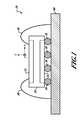
- FIGURE 1illustrates an example integrated 3-axis magnetic sensor 20 formed in accordance with one embodiment.
- the sensor 20includes a die 30 that has one or two in-plane (x, y-axis) magnetic sensing elements on one side of the die 30 and an out-of-plane (z-axis) magnetic sensing element on an opposing side of the die 30 - see sensing element(s) 32 and 34. Examples of in-plane and out-of-plane sensing elements are described in U.S. Patent No. 7,126,330 , which is hereby incorporated by reference.
- the die 30is attached both mechanically and electrically to a circuit board 60 by interconnection bump(s) 38.
- the bump(s) 38may be formed of any of a number of electrically conductive materials that are bondable (e.g., solder) to both the die 30 and the circuit board 60. Examples of Restriction of Hazardous Substances (RoHS) bump materials are SnAgCu and SnAg, and non-RoHS is SnPb.
- the bump(s) 38connect to electrical traces (not shown) on the sensing element(s) 34 and on the circuit board 60 using a re-flow process.
- one or more wires 40are soldered or somehow otherwise physically attached to predefined locations on the sensing element(s) 32 side of the die 30 and the circuit board 60 in order to electrically connect to traces on the circuit board 60 and on or in proximity to the sensing element(s) 34.
- FIGURE 2illustrates a portion of a cross-sectional view of the die 30 of FIGURE 1 .
- An example fabrication for the die 30includes forming on a first surface of a silicon wafer 42 the first sensing element(s) 32 via standard masking and etching techniques for magneto resistive sensors based on a predefined pattern for the desired sensing element.
- the wafer 42is a silicon-on-insulator (SOI) wafer that has a buried dielectric (oxide) layer 44 and the sensing element 42 is etched into a layer of silicon that is located on a top of the dielectric layer 44.
- SOIsilicon-on-insulator
- a metallization (interconnection) layer 46is applied accordingly to a predefined pattern, thus producing traces that connect to the sensing element(s) 32.
- Au and Alare typical metals used for the metallization (interconnection) layer 46.
- a scratch protection (passivation) layer 50is applied to protect the sensing element(s) 32 and metallization layer 46 from scratching and chemical degradation caused during the fabrication of the sensing element(s) 34 on the opposing side of the die 30 and during assembly on the substrate.
- the second sensing element(s) 34is formed onto the second side of the die 30.
- the second sensing element 34is formed directly into the wafer starting with creating at least one sloping surface.
- a metallization (interconnection) layer 48is applied over the sensing element(s) 34 according to a predefined pattern similar to the layer 46.
- the interconnection bump(s) 38is electrically and mechanically bonded to the metallization (interconnection) layer 48 via soldering and some other known technique.
- a scratch protection layer 58is applied over the metallization (interconnection) layer 48 and the sensing element(s) 34.
- the scratch protection layer 58is then etched in order to expose a section of the metallization (interconnection) layer 48 for allowing connection of the bump 38. Finally, the scratch protection layer 50 that is applied to the top surface of the die 30 is removed at predefined locations in order to allow for connection of the wires 40 to the metallization layer 46.
- FIGURE 3illustrates an alternate embodiment of an integrated 3-axis magnetic sensor 100.
- the magnetic sensor 100includes a die 106 with a first sensing element(s) 108 located on a first side of the die 106 and a second sensing element(s) 110 located on a second side of the die 106.
- the sensing elements 108 and 110are formed in a similar manner to that described above with regard to FIGURES 1 and 2 and with regard to U.S. Patent No. 7,126,330 .
- the sensor 100includes one or more vias 112 formed within the die 106 for electrically connecting the first sensing 108 with electrical leads on the second side of the die 106. This allows signals to be passed between the first sensing element 108 and circuit components (not shown) located on a circuit board 120 via bumps 114 that connect the die 106 to the circuit board 120.
- the second sensing element(s) 110is formed on the second side of a silicon wafer 126.
- a metallization (interconnection) layer 130is formed on the portions of the first sensing element(s) 110.
- a protection layer 134is formed over the metallization (interconnection) layer 130 and the second sensing element(s) 110 - similar to FIGURE 2 .
- a via(s) 112is formed by etching away the silicon wafer 126 from the first side to the metallization (interconnection) layer 130 using any number of predefined etching techniques (e.g., KOH etch, RIE).
- the via(s) 112may be formed before or after the first sensing element(s) 108 has been formed on the first side of the wafer 126. After the via(s) 112 is formed, then a metallization (interconnection) layer 136 is applied according to a predefined pattern in order to electrically connect the first sensing element(s) 108 to the second side of the wafer 126 via the metallization layer 136. A scratch protection layer 134 is optionally applied over the first side that includes the metallization (interconnection) layer 136 and the first sensing element 108.
- the scratch protection layer 134is removed (e.g., section 140) to expose a portion of the metallization (interconnection) layer 130 at predefined locations. Then, one or more bumps 114 are bonded to the exposed metallization layer 130. This allows signals to be communicated between electric components on the circuit board 120 and any of the sensing elements 108, 110.
- FIGURE 5illustrates another embodiment of the present invention that is a combination of those shown in FIGURES 1 and 3 to produce a sensor 180.
- the bumps 38 or 114are not included.
- the die 106is similar to that shown in FIGURE 3 with sensing elements108, 110 on opposing sides of the die with vias 112 through the die 106. However, the die 106 is directly attached to the circuit board 120 (no bumps) and the sensing elements108, 110 are electrically attached to the circuit board 120 by one or more lead wires 140 attached similar to wires 40.
- two sensors 150, 152are formed or attached to sloped surfaces on one side of a die 154.
- the previously etched sloped surfacesallow the sensors 150, 152 to measure orthogonal fields/forces. This is described in more detail in U.S. Patent No. 7,126,330 .
- the fabrication stepsmay be performed in any of a number of different orders.
- some layerssuch as the protection layer may be an optional addition.
- the sensorsmay be other type of field sensors, such as electric, gravitational, etc.
- the sensorsmay be any of a number of different types that measure a field or force (e.g., acceleration). Accordingly, the scope of the invention is not limited by the disclosure of the preferred embodiment. Instead, the invention should be determined entirely by reference to the claims that follow.
Landscapes
- Physics & Mathematics (AREA)
- Condensed Matter Physics & Semiconductors (AREA)
- General Physics & Mathematics (AREA)
- Measuring Magnetic Variables (AREA)
- Hall/Mr Elements (AREA)
Abstract
Description
- Magnetic sensing devices facilitate the measurement of a magnetic field (i.e. one or more magnetic fields) for a variety of applications by using one or more magnetic sensor units to sense the magnetic field, and to provide output signals that represent the magnetic field. Navigation applications that determine a heading determination are popular applications for magnetic sensing devices. A heading determination may indicate a direction, such as North or North-East. Other applications for magnetic sensing devices, such as proximity detection, are also possible.
- The one or more magnetic sensor units in a magnetic sensing device may be arranged in a manner that provides sensing of particular components of a magnetic field. For example, a first magnetic sensor unit may be arranged to sense a component of a magnetic field in a direction defined as the x-axis direction, and a second magnetic sensor unit may be arranged to sense a component of the magnetic field in a direction defined as the y-axis direction. In this example, the magnetic sensing device could have a first output to provide an output signal that represents components of the magnetic field in the x-axis direction and a second output to provide an output signal that represents components of the magnetic field in the y-axis direction.
- A wide variety of magnetic sensor unit types are available such as reed switches, variable reluctance sensors, flux-gate magnetometers, magneto-inductor sensors, spin-tunnel device sensors, and Hall-Effect sensors. Another magnetic sensor unit type is a magnetic sensor unit that comprises magnetoresistive material. Examples of magnetic sensors comprising magnetoresistive material include giant magneto-resistive sensors and giant magneto-impedance sensors. Other examples are also possible.
- Magnetoresistive material is a material with a variable resistance value that varies depending in part on a magnetic field in proximity to the magnetoresistive material. The sensitivity of magnetoresistive material to change its resistance value when exposed to a magnetic field depends in part on the characteristics of a particular magnetoresistive material. Common magnetoresistive materials include anisotropic magnetoresistive (AMR) materials and giant magnetoresistive (GMR) materials which are both described in
U.S. Pat. No. 5,569,544 and colossal magnetoresistive (CMR) materials described inU.S. Pat. No. 5,982,178 . One type of AMR material is a nickel-iron material known as Permalloy. AMR-type magnetic sensor units may include thin films of Permalloy deposited on a silicon wafer and patterned as a resistor. Multiple resistors made of Permalloy may be coupled together to form an electrical circuit. The electrical circuit could take the form of a bridge configuration, such as a Wheatstone bridge configuration. - Magnetic sensing devices are available in a variety of one-axis and two-axis configurations. The number of axes in a magnetic sensing device refers to the number of sensitive axes or sensing directions for measuring a magnetic field. Magnetic sensing devices with more than one axis typically arrange the multiple axes to be mutually orthogonal. Some forms of three-axis magnetic sensing devices are available but not in the integrated forms as described below.
- The present invention provides a multi-axis (magnetic) field sensing device and method of fabricating a multi-axis (magnetic) field sensing device. An example sensing device is a 3-axis sensor package on a substrate with sensors on opposing sides of the substrate. One side of the substrate includes an X-axis sensor and a Y-axis sensor (or alternatively an integrated X-Y-axis sensor) and the opposite side of the substrate includes a Z-axis sensor on at least one sloped surface, the surface sloped with respect to both the first and second surface areas. One surface is mechanically and electrically bonded to a circuit board via conductive bumps. The other surface electrically connects to the circuit board through bonded wires and/or vias formed through the substrate.
- Preferred and alternative embodiments of the present invention are described in detail below with reference to the following drawings:
FIGURE 1 illustrates a side view of an exemplary 3-axis magnetic sensor;FIGURE 2 illustrates a partial cross-sectional view of an example of the sensor shown onFIGURE 1 ;FIGURE 3 illustrates a 3-axis magnetic sensor formed in accordance with an alternate embodiment of the present invention;FIGURE 4 illustrates a partial cross-sectional view of an example of the sensor shown onFIGURE 3 ;FIGURE 5 illustrates a partial cross-sectional view of another example of the present invention; andFIGURE 6 illustrates a zoomed cross-sectional view of two sensing elements located on the same side of a die.FIGURE 1 illustrates an example integrated 3-axismagnetic sensor 20 formed in accordance with one embodiment. Thesensor 20 includes adie 30 that has one or two in-plane (x, y-axis) magnetic sensing elements on one side of the die 30 and an out-of-plane (z-axis) magnetic sensing element on an opposing side of the die 30 - see sensing element(s) 32 and 34. Examples of in-plane and out-of-plane sensing elements are described inU.S. Patent No. 7,126,330 , which is hereby incorporated by reference.- The die 30 is attached both mechanically and electrically to a
circuit board 60 by interconnection bump(s) 38. The bump(s) 38 may be formed of any of a number of electrically conductive materials that are bondable (e.g., solder) to both thedie 30 and thecircuit board 60. Examples of Restriction of Hazardous Substances (RoHS) bump materials are SnAgCu and SnAg, and non-RoHS is SnPb. The bump(s) 38 connect to electrical traces (not shown) on the sensing element(s) 34 and on thecircuit board 60 using a re-flow process. - Because the sensing element(s) 32 is located on the opposing side of the
die 30 from the sensing element(s) 34, and is electrically isolated from the sensing element(s) 34 as well as the circuit board 60 (and the bump(s) 38), one ormore wires 40 are soldered or somehow otherwise physically attached to predefined locations on the sensing element(s) 32 side of thedie 30 and thecircuit board 60 in order to electrically connect to traces on thecircuit board 60 and on or in proximity to the sensing element(s) 34. FIGURE 2 illustrates a portion of a cross-sectional view of the die 30 ofFIGURE 1 . An example fabrication for the die 30 includes forming on a first surface of asilicon wafer 42 the first sensing element(s) 32 via standard masking and etching techniques for magneto resistive sensors based on a predefined pattern for the desired sensing element. In an optional embodiment, thewafer 42 is a silicon-on-insulator (SOI) wafer that has a buried dielectric (oxide) layer 44 and thesensing element 42 is etched into a layer of silicon that is located on a top of the dielectric layer 44. After the sensing element(s) 32 has been formed, a metallization (interconnection)layer 46 is applied accordingly to a predefined pattern, thus producing traces that connect to the sensing element(s) 32. Au and Al are typical metals used for the metallization (interconnection)layer 46. Then, a scratch protection (passivation)layer 50 is applied to protect the sensing element(s) 32 andmetallization layer 46 from scratching and chemical degradation caused during the fabrication of the sensing element(s) 34 on the opposing side of thedie 30 and during assembly on the substrate.- Next, the second sensing element(s) 34 is formed onto the second side of the die 30. The
second sensing element 34 is formed directly into the wafer starting with creating at least one sloping surface. Then, a metallization (interconnection)layer 48 is applied over the sensing element(s) 34 according to a predefined pattern similar to thelayer 46. Then, the interconnection bump(s) 38 is electrically and mechanically bonded to the metallization (interconnection)layer 48 via soldering and some other known technique. Next, ascratch protection layer 58 is applied over the metallization (interconnection)layer 48 and the sensing element(s) 34. Thescratch protection layer 58 is then etched in order to expose a section of the metallization (interconnection)layer 48 for allowing connection of thebump 38. Finally, thescratch protection layer 50 that is applied to the top surface of thedie 30 is removed at predefined locations in order to allow for connection of thewires 40 to themetallization layer 46. FIGURE 3 illustrates an alternate embodiment of an integrated 3-axismagnetic sensor 100. Themagnetic sensor 100 includes adie 106 with a first sensing element(s) 108 located on a first side of the die 106 and a second sensing element(s) 110 located on a second side of the die 106. Thesensing elements FIGURES 1 and2 and with regard toU.S. Patent No. 7,126,330 . Thesensor 100 includes one ormore vias 112 formed within thedie 106 for electrically connecting thefirst sensing 108 with electrical leads on the second side of thedie 106. This allows signals to be passed between thefirst sensing element 108 and circuit components (not shown) located on acircuit board 120 viabumps 114 that connect thedie 106 to thecircuit board 120.- As shown in
FIGURE 4 , after the second sensing element(s) 110 is formed on the second side of asilicon wafer 126. A metallization (interconnection)layer 130 is formed on the portions of the first sensing element(s) 110. Then, aprotection layer 134 is formed over the metallization (interconnection)layer 130 and the second sensing element(s) 110 - similar toFIGURE 2 . Next, a via(s) 112 is formed by etching away thesilicon wafer 126 from the first side to the metallization (interconnection)layer 130 using any number of predefined etching techniques (e.g., KOH etch, RIE). The via(s) 112 may be formed before or after the first sensing element(s) 108 has been formed on the first side of thewafer 126. After the via(s) 112 is formed, then a metallization (interconnection)layer 136 is applied according to a predefined pattern in order to electrically connect the first sensing element(s) 108 to the second side of thewafer 126 via themetallization layer 136. Ascratch protection layer 134 is optionally applied over the first side that includes the metallization (interconnection)layer 136 and thefirst sensing element 108. Finally, in order to connect the die 106 mechanically and electrically to thecircuit board 120, thescratch protection layer 134 is removed (e.g., section 140) to expose a portion of the metallization (interconnection)layer 130 at predefined locations. Then, one ormore bumps 114 are bonded to the exposedmetallization layer 130. This allows signals to be communicated between electric components on thecircuit board 120 and any of thesensing elements FIGURE 5 illustrates another embodiment of the present invention that is a combination of those shown inFIGURES 1 and3 to produce asensor 180. Thebumps die 106 is similar to that shown inFIGURE 3 with sensing elements108, 110 on opposing sides of the die withvias 112 through thedie 106. However, thedie 106 is directly attached to the circuit board 120 (no bumps) and the sensing elements108, 110 are electrically attached to thecircuit board 120 by one or morelead wires 140 attached similar towires 40.- As shown in
FIGURE 6 , twosensors die 154. The previously etched sloped surfaces allow thesensors U.S. Patent No. 7,126,330 . - While the preferred embodiment of the invention has been illustrated and described, as noted above, many changes can be made without departing from the spirit and scope of the invention. For example, the fabrication steps may be performed in any of a number of different orders. Also, some layers such as the protection layer may be an optional addition. Also, the sensors may be other type of field sensors, such as electric, gravitational, etc. The sensors may be any of a number of different types that measure a field or force (e.g., acceleration). Accordingly, the scope of the invention is not limited by the disclosure of the preferred embodiment. Instead, the invention should be determined entirely by reference to the claims that follow.
- The embodiments of the invention in which an exclusive property or privilege is claimed are defined as follows:
Claims (11)
Applications Claiming Priority (1)
| Application Number | Priority Date | Filing Date | Title |
|---|---|---|---|
| US11/877,537US7564237B2 (en) | 2007-10-23 | 2007-10-23 | Integrated 3-axis field sensor and fabrication methods |
Publications (3)
| Publication Number | Publication Date |
|---|---|
| EP2053415A2true EP2053415A2 (en) | 2009-04-29 |
| EP2053415A3 EP2053415A3 (en) | 2010-10-06 |
| EP2053415B1 EP2053415B1 (en) | 2011-06-29 |
Family
ID=40266038
Family Applications (1)
| Application Number | Title | Priority Date | Filing Date |
|---|---|---|---|
| EP08166849ACeasedEP2053415B1 (en) | 2007-10-23 | 2008-10-16 | Integrated 3-axis field sensor and fabrication methods |
Country Status (4)
| Country | Link |
|---|---|
| US (1) | US7564237B2 (en) |
| EP (1) | EP2053415B1 (en) |
| JP (1) | JP5465861B2 (en) |
| KR (1) | KR101501929B1 (en) |
Families Citing this family (13)
| Publication number | Priority date | Publication date | Assignee | Title |
|---|---|---|---|---|
| US8390283B2 (en) | 2009-09-25 | 2013-03-05 | Everspin Technologies, Inc. | Three axis magnetic field sensor |
| US20110234218A1 (en)* | 2010-03-24 | 2011-09-29 | Matthieu Lagouge | Integrated multi-axis hybrid magnetic field sensor |
| US8518734B2 (en) | 2010-03-31 | 2013-08-27 | Everspin Technologies, Inc. | Process integration of a single chip three axis magnetic field sensor |
| RU2470410C2 (en)* | 2010-12-28 | 2012-12-20 | Федеральное Государственное Учреждение "Научно-Производственный Комплекс "Технологический Центр" Московского Государственного Института Электронной Техники" | Method of making microsystem for detecting three magnetic induction vector components |
| CN102426344B (en)* | 2011-08-30 | 2013-08-21 | 江苏多维科技有限公司 | Three-axis magnetic field sensor |
| US20130257423A1 (en)* | 2012-04-03 | 2013-10-03 | Isentek Inc. | Hybrid magnetic sensor |
| WO2014059110A1 (en)* | 2012-10-12 | 2014-04-17 | Memsic, Inc. | Monolithic three-axis magnetic field sensor |
| KR102282640B1 (en)* | 2014-11-24 | 2021-07-27 | 주식회사 키 파운드리 | Method for manufacturing of Semiconductor Device Having a Buried Magnetic Sensor |
| RU175590U1 (en)* | 2017-04-25 | 2017-12-11 | Российская Федерация, от имени которой выступает Федеральное государственное казенное учреждение "Войсковая часть 68240" | THREE-AXIS MICROSYSTEM ANALYSIS OF WEAK MAGNETIC FIELDS |
| JP7064662B2 (en)* | 2017-04-25 | 2022-05-11 | コニカミノルタ株式会社 | Magnetic sensor |
| US11193989B2 (en)* | 2018-07-27 | 2021-12-07 | Allegro Microsystems, Llc | Magnetoresistance assembly having a TMR element disposed over or under a GMR element |
| EP3675172B8 (en)* | 2018-12-24 | 2023-10-18 | Crocus Technology Sa | Magnetic reader sensor device for reading magnetic stripes and method for manufacturing the sensor device |
| CN114114102B (en)* | 2021-11-18 | 2024-01-23 | 中国人民解放军国防科技大学 | Integrated planarization triaxial magnetic sensor and application method thereof |
Citations (5)
| Publication number | Priority date | Publication date | Assignee | Title |
|---|---|---|---|---|
| US5569544A (en) | 1992-11-16 | 1996-10-29 | Nonvolatile Electronics, Incorporated | Magnetoresistive structure comprising ferromagnetic thin films and intermediate layers of less than 30 angstroms formed of alloys having immiscible components |
| US5982178A (en) | 1997-12-18 | 1999-11-09 | Honewell Inc. | Method and apparatus for sensing a desired component of an incident magnetic field using magneto resistive elements biased in different directions |
| US20020153876A1 (en) | 2001-04-09 | 2002-10-24 | De Jong Franciscus Gerardus Maria | Integrated circuit with power supply test interface |
| US20050122101A1 (en) | 2003-12-04 | 2005-06-09 | Honeywell International Inc. | Single package design for 3-axis magnetic sensor |
| US20050122100A1 (en) | 2003-12-04 | 2005-06-09 | Honeywell International Inc. | Vertical die chip-on-board |
Family Cites Families (11)
| Publication number | Priority date | Publication date | Assignee | Title |
|---|---|---|---|---|
| JPS6311672Y2 (en)* | 1980-12-22 | 1988-04-05 | ||
| JPS63150384U (en)* | 1987-03-24 | 1988-10-04 | ||
| JP2579995B2 (en)* | 1988-03-31 | 1997-02-12 | 株式会社東芝 | Magnetic sensor |
| JPH08167747A (en)* | 1994-12-12 | 1996-06-25 | Hitachi Cable Ltd | Hall sensor |
| FR2750769B1 (en)* | 1996-07-05 | 1998-11-13 | Thomson Csf | THIN FILM MAGNETIC FIELD SENSOR |
| JP2003161770A (en)* | 2001-11-27 | 2003-06-06 | Fuji Electric Co Ltd | Magnetic sensing element |
| JP4085859B2 (en)* | 2002-03-27 | 2008-05-14 | ヤマハ株式会社 | Magnetic sensor and manufacturing method thereof |
| US7126330B2 (en)* | 2004-06-03 | 2006-10-24 | Honeywell International, Inc. | Integrated three-dimensional magnetic sensing device and method to fabricate an integrated three-dimensional magnetic sensing device |
| JP4453536B2 (en)* | 2004-12-10 | 2010-04-21 | トヨタ自動車株式会社 | Drive device, automobile equipped with the drive device, and control method of drive device |
| JP4613661B2 (en)* | 2005-03-29 | 2011-01-19 | ヤマハ株式会社 | Manufacturing method of 3-axis magnetic sensor |
| US7768083B2 (en)* | 2006-01-20 | 2010-08-03 | Allegro Microsystems, Inc. | Arrangements for an integrated sensor |
- 2007
- 2007-10-23USUS11/877,537patent/US7564237B2/enactiveActive
- 2008
- 2008-10-16EPEP08166849Apatent/EP2053415B1/ennot_activeCeased
- 2008-10-21JPJP2008271064Apatent/JP5465861B2/enactiveActive
- 2008-10-22KRKR1020080103858Apatent/KR101501929B1/enactiveActive
Patent Citations (5)
| Publication number | Priority date | Publication date | Assignee | Title |
|---|---|---|---|---|
| US5569544A (en) | 1992-11-16 | 1996-10-29 | Nonvolatile Electronics, Incorporated | Magnetoresistive structure comprising ferromagnetic thin films and intermediate layers of less than 30 angstroms formed of alloys having immiscible components |
| US5982178A (en) | 1997-12-18 | 1999-11-09 | Honewell Inc. | Method and apparatus for sensing a desired component of an incident magnetic field using magneto resistive elements biased in different directions |
| US20020153876A1 (en) | 2001-04-09 | 2002-10-24 | De Jong Franciscus Gerardus Maria | Integrated circuit with power supply test interface |
| US20050122101A1 (en) | 2003-12-04 | 2005-06-09 | Honeywell International Inc. | Single package design for 3-axis magnetic sensor |
| US20050122100A1 (en) | 2003-12-04 | 2005-06-09 | Honeywell International Inc. | Vertical die chip-on-board |
Also Published As
| Publication number | Publication date |
|---|---|
| EP2053415B1 (en) | 2011-06-29 |
| KR101501929B1 (en) | 2015-03-12 |
| US20090102475A1 (en) | 2009-04-23 |
| JP5465861B2 (en) | 2014-04-09 |
| US7564237B2 (en) | 2009-07-21 |
| EP2053415A3 (en) | 2010-10-06 |
| KR20090041344A (en) | 2009-04-28 |
| JP2009168796A (en) | 2009-07-30 |
Similar Documents
| Publication | Publication Date | Title |
|---|---|---|
| EP2053415B1 (en) | Integrated 3-axis field sensor and fabrication methods | |
| EP2267470B1 (en) | Integrated three-dimensional magnetic sensing device and fabrication method | |
| US7095226B2 (en) | Vertical die chip-on-board | |
| JP5157611B2 (en) | Magnetic sensor and manufacturing method thereof | |
| US8742520B2 (en) | Three axis magnetic sensor device and method | |
| US8981773B2 (en) | Magnetoresistive sensor with reduced parasitic capacitance, and method | |
| US10353020B2 (en) | Manufacturing method for integrated multilayer magnetoresistive sensor | |
| EP2752676B1 (en) | Triaxial magnetic field sensor | |
| EP2656090A1 (en) | Integrated magnetoresistive sensor, in particular three-axes magnetoresistive sensor and manufacturing method thereof | |
| JP5140291B2 (en) | Motion sensor | |
| JP2015520840A (en) | Foldable board | |
| EP3462201B1 (en) | Magnetic field sensor with coil structure and method of fabrication | |
| CN111044951B (en) | Three-axis magnetic field sensor and manufacturing method thereof | |
| RU2470410C2 (en) | Method of making microsystem for detecting three magnetic induction vector components | |
| WO2006134520A1 (en) | Magnetic field sensor device |
Legal Events
| Date | Code | Title | Description |
|---|---|---|---|
| PUAI | Public reference made under article 153(3) epc to a published international application that has entered the european phase | Free format text:ORIGINAL CODE: 0009012 | |
| 17P | Request for examination filed | Effective date:20081016 | |
| AK | Designated contracting states | Kind code of ref document:A2 Designated state(s):AT BE BG CH CY CZ DE DK EE ES FI FR GB GR HR HU IE IS IT LI LT LU LV MC MT NL NO PL PT RO SE SI SK TR | |
| AX | Request for extension of the european patent | Extension state:AL BA MK RS | |
| PUAL | Search report despatched | Free format text:ORIGINAL CODE: 0009013 | |
| AK | Designated contracting states | Kind code of ref document:A3 Designated state(s):AT BE BG CH CY CZ DE DK EE ES FI FR GB GR HR HU IE IS IT LI LT LU LV MC MT NL NO PL PT RO SE SI SK TR | |
| AX | Request for extension of the european patent | Extension state:AL BA MK RS | |
| RIC1 | Information provided on ipc code assigned before grant | Ipc:G01R 33/02 20060101AFI20090128BHEP Ipc:G01R 33/00 20060101ALI20100901BHEP | |
| 17Q | First examination report despatched | Effective date:20100923 | |
| GRAP | Despatch of communication of intention to grant a patent | Free format text:ORIGINAL CODE: EPIDOSNIGR1 | |
| RIC1 | Information provided on ipc code assigned before grant | Ipc:G01R 33/00 20060101ALI20110214BHEP Ipc:G01R 33/02 20060101AFI20110214BHEP | |
| GRAS | Grant fee paid | Free format text:ORIGINAL CODE: EPIDOSNIGR3 | |
| GRAA | (expected) grant | Free format text:ORIGINAL CODE: 0009210 | |
| REG | Reference to a national code | Ref country code:DE Ref legal event code:8566 Ref country code:DE Ref legal event code:R108 Effective date:20110322 | |
| AKX | Designation fees paid | Designated state(s):FI | |
| AK | Designated contracting states | Kind code of ref document:B1 Designated state(s):FI | |
| PLBE | No opposition filed within time limit | Free format text:ORIGINAL CODE: 0009261 | |
| STAA | Information on the status of an ep patent application or granted ep patent | Free format text:STATUS: NO OPPOSITION FILED WITHIN TIME LIMIT | |
| 26N | No opposition filed | Effective date:20120330 | |
| PGFP | Annual fee paid to national office [announced via postgrant information from national office to epo] | Ref country code:FI Payment date:20181022 Year of fee payment:11 | |
| REG | Reference to a national code | Ref country code:FI Ref legal event code:MAE | |
| PG25 | Lapsed in a contracting state [announced via postgrant information from national office to epo] | Ref country code:FI Free format text:LAPSE BECAUSE OF NON-PAYMENT OF DUE FEES Effective date:20191016 | |
| P01 | Opt-out of the competence of the unified patent court (upc) registered | Effective date:20230525 |