EP2045791B1 - An electronic device - Google Patents
An electronic deviceDownload PDFInfo
- Publication number
- EP2045791B1 EP2045791B1EP07019294.3AEP07019294AEP2045791B1EP 2045791 B1EP2045791 B1EP 2045791B1EP 07019294 AEP07019294 AEP 07019294AEP 2045791 B1EP2045791 B1EP 2045791B1
- Authority
- EP
- European Patent Office
- Prior art keywords
- converter
- wire line
- electronic device
- current
- information signal
- Prior art date
- Legal status (The legal status is an assumption and is not a legal conclusion. Google has not performed a legal analysis and makes no representation as to the accuracy of the status listed.)
- Not-in-force
Links
Images
Classifications
- G—PHYSICS
- G08—SIGNALLING
- G08C—TRANSMISSION SYSTEMS FOR MEASURED VALUES, CONTROL OR SIMILAR SIGNALS
- G08C19/00—Electric signal transmission systems
- G08C19/02—Electric signal transmission systems in which the signal transmitted is magnitude of current or voltage
Definitions
- the present inventionrelates to an electronic device having an interface circuit for communicating with and receiving power from a two-wire line, said interface circuit comprising a modulation means connected to the two-wire line and responsive to an information signal for modulating the current in the two-wire line according to the information signal, and further comprising a controllable switching type DC-to-DC converter for extracting power for the electronic device from the two-wire line.
- Such an electronic deviceis known from US 6,907,082 , US 6,972,584 or GB 2 229 897 .
- the modulation meanscomprises a variable resistor constituted by the collector-emitter path of a transistor.
- the transistorneeds a minimum voltage drop across the collector-emitter path to properly work as a controllable current sink, and the current is controlled by adjusting this voltage drop which causes power dissipation.
- this objectis achieved by the electronic device of the type initially mentioned in that the DC-to-DC converter is modified to be controlled by said information signal and to perform the function of the modulation means. That is, the current sink function is implemented in a switched mode fashion.
- the modified DC-to-DC converternearly losslessly converts the two-wire line voltage to a feeding voltage for the electronic device, where the control is changed from controlling the output voltage of the DC-to-DC converter to controlling its input current.
- the input currentis used as the feedback variable and therefore is controlled by the switching duty cycle of the modified DC-to-DC converter in that the output voltage is not regulated.
- the output voltage of the DC-to-DC convertershould be limited by whatever value and method is more appropriated for the electronic device components being feed by the output voltage, such as a simple zener diode or a shunt regulator.
- the modified DC-to-DC converterhas only a current control loop and the usually present output capacitor is not part of the control loop, the restrictions of a conventionally used DC-to-DC converter to increase the bandwidth are removed. This allows for controlling and modulating the current in the two-wire line.
- the modified DC-to-DC convertermay be of any switched topology with or without features to minimize switching losses as using resonant circuits.
- switching circuit topologies with inherent input inductor like a boost and Cuk converterare used, the advantage of which is that it creates a smooth current at input and allows higher bandwidth for controlling the input current.
- the electronic deviceis typically a field device for process automation, such as a measuring transducer, but may also be any other device being powered and communicating over a two-wire line with a variety of communication protocols.
- Examples of communication protocolsinclude analog 4 to 20 mA, HART, PROFIBUS PA and FOUNDATION Fieldbus.
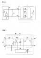
- FIG. 1exemplarily shows the basic components of a two-wire system including a DC-powered electronic device 1, here a measuring transducer for process automation, responsive to a process variable measured by a sensor 2.
- the electronic device 1is linked by a two-wire line 3 to a remote receiving station 4 in which a DC power supply 5 is connected in series with a current sensing resistor 6.
- the voltage across the current sensing resistor 6is applied to a receiver 7 which may be a process variable indicator, recorder, a controller and any other device appropriate to process control.
- the electronic device 1comprises an interface circuit 8 providing an interface between the two-wire line 3 and remaining circuit components of the device 1.
- These componentsinclude in particular a microcontroller 9 which receives a signal from the sensor 2 and, after processing it to an information signal 10 representative of the value of the process variable, controls the interface circuit 8 to transmit this value onto the two-wire line 3.
- the circuit components including the microcontroller 9are powered from the power supply 5 via the two-wire line 3 and the interface circuit 8.
- FIG. 2shows an embodiment of the interface circuit 8 which comprises a controllable switching type DC-to-DC converter 11 having input terminals 12, 13 coupled to the two-wire line 3 and output terminals 14, 15 coupled to the supply lines of the circuit components of the device 1.
- the DC-to-DC converter 11serves the double purpose of supplying energy from the two-wire line 3 to the components of the device 1 and for transmitting the information signal 10 onto the two-wire line 3.
- a controller 16generates a modulation signal 17 for modulating the current i on the two-wire line 3 in response to the information signal 10 and the actual current i measured by a current probe R.
- the DC-to-DC converter 11is configured as a Cuk converter and includes an input inductor L1 connected to terminal 12, an output inductor L2 connected to terminal 14, an energy transfer capacitor C1 connected between the two inductors L1, L2 and two switches Q and D configured to alternately tie the inductors L1 or L2 to a common connection.
- transistor switch Qis configured to be controlled by the modulation signal 17 and diode switch D is configured to switch ON and OFF in response to the switching of transistor Q.
- the function of a Cuk converteris well known and therefore does not require a particular specific description.
- the remote station 4may include additional means (not shown) for transmitting information such as parameters to the device 1 by modulating the voltage across the two-wire line 3.
- the resulting voltage variationscan be detected in the device 1 by line 18 and fed to the controller 16 for forwarding the received information 19 to the microcontroller 9.
Landscapes
- Physics & Mathematics (AREA)
- General Physics & Mathematics (AREA)
- Arrangements For Transmission Of Measured Signals (AREA)
- Dc-Dc Converters (AREA)
Description
- The present invention relates to an electronic device having an interface circuit for communicating with and receiving power from a two-wire line, said interface circuit comprising a modulation means connected to the two-wire line and responsive to an information signal for modulating the current in the two-wire line according to the information signal, and further comprising a controllable switching type DC-to-DC converter for extracting power for the electronic device from the two-wire line.
- In the known devices, the modulation means comprises a variable resistor constituted by the collector-emitter path of a transistor. The transistor needs a minimum voltage drop across the collector-emitter path to properly work as a controllable current sink, and the current is controlled by adjusting this voltage drop which causes power dissipation.
- It is therefore an object of the invention to reduce or completely eliminate such losses.
- According to the invention this object is achieved by the electronic device of the type initially mentioned in that the DC-to-DC converter is modified to be controlled by said information signal and to perform the function of the modulation means. That is, the current sink function is implemented in a switched mode fashion.
- The modified DC-to-DC converter nearly losslessly converts the two-wire line voltage to a feeding voltage for the electronic device, where the control is changed from controlling the output voltage of the DC-to-DC converter to controlling its input current. In the changed control the input current is used as the feedback variable and therefore is controlled by the switching duty cycle of the modified DC-to-DC converter in that the output voltage is not regulated. The output voltage of the DC-to-DC converter should be limited by whatever value and method is more appropriated for the electronic device components being feed by the output voltage, such as a simple zener diode or a shunt regulator. As the modified DC-to-DC converter has only a current control loop and the usually present output capacitor is not part of the control loop, the restrictions of a conventionally used DC-to-DC converter to increase the bandwidth are removed. This allows for controlling and modulating the current in the two-wire line.
- The modified DC-to-DC converter may be of any switched topology with or without features to minimize switching losses as using resonant circuits. Preferably, switching circuit topologies with inherent input inductor like a boost and Cuk converter are used, the advantage of which is that it creates a smooth current at input and allows higher bandwidth for controlling the input current.
- The electronic device is typically a field device for process automation, such as a measuring transducer, but may also be any other device being powered and communicating over a two-wire line with a variety of communication protocols. Examples of communication protocols include analog 4 to 20 mA, HART, PROFIBUS PA and FOUNDATION Fieldbus.
- The invention will be now described by way of preferred examples and with reference to the accompanying drawing, in which:
- Figure 1
- shows a block diagram of a two-wire system including an electronic device according to the invention having an interface circuit for communicating over and receiving power from the two-wire system, and
- Figure 2
- shows a block diagram of the interface circuit.
- Reference is first made to
Figure 1 which exemplarily shows the basic components of a two-wire system including a DC-poweredelectronic device 1, here a measuring transducer for process automation, responsive to a process variable measured by asensor 2. Theelectronic device 1 is linked by a two-wire line 3 to aremote receiving station 4 in which aDC power supply 5 is connected in series with acurrent sensing resistor 6. The voltage across thecurrent sensing resistor 6 is applied to areceiver 7 which may be a process variable indicator, recorder, a controller and any other device appropriate to process control. Theelectronic device 1 comprises aninterface circuit 8 providing an interface between the two-wire line 3 and remaining circuit components of thedevice 1. These components include in particular amicrocontroller 9 which receives a signal from thesensor 2 and, after processing it to aninformation signal 10 representative of the value of the process variable, controls theinterface circuit 8 to transmit this value onto the two-wire line 3. The circuit components including themicrocontroller 9 are powered from thepower supply 5 via the two-wire line 3 and theinterface circuit 8. Figure 2 shows an embodiment of theinterface circuit 8 which comprises a controllable switching type DC-to-DC converter 11 havinginput terminals wire line 3 andoutput terminals device 1. The DC-to-DC converter 11 serves the double purpose of supplying energy from the two-wire line 3 to the components of thedevice 1 and for transmitting theinformation signal 10 onto the two-wire line 3. Acontroller 16 generates amodulation signal 17 for modulating the current i on the two-wire line 3 in response to theinformation signal 10 and the actual current i measured by a current probe R. The DC-to-DC converter 11 is configured as a Cuk converter and includes an input inductor L1 connected toterminal 12, an output inductor L2 connected toterminal 14, an energy transfer capacitor C1 connected between the two inductors L1, L2 and two switches Q and D configured to alternately tie the inductors L1 or L2 to a common connection. Specifically, transistor switch Q is configured to be controlled by themodulation signal 17 and diode switch D is configured to switch ON and OFF in response to the switching of transistor Q. The function of a Cuk converter is well known and therefore does not require a particular specific description.- The
remote station 4 may include additional means (not shown) for transmitting information such as parameters to thedevice 1 by modulating the voltage across the two-wire line 3. The resulting voltage variations can be detected in thedevice 1 byline 18 and fed to thecontroller 16 for forwarding the receivedinformation 19 to themicrocontroller 9.
Claims (3)
- An electronic device (1) having an interface circuit (8) for communicating with and receiving power from a two-wire line (3), said interface circuit (8) comprising
a modulation means connected to the two-wire line (3) and responsive to an information signal (10) for modulating the current in the two-wire line (3) according to the information signal (10), and further comprising
a controllable switching type DC-to-DC converter (11) for extracting power for the electronic device (1) from the two-wire line (3),characterized in that
the DC-to-DC converter (11) is designed to be controlled by said information signal (10) and configured to modulate the current in the two-wire line according to said information signal. - The electronic device (1) according to claim 1,characterized in that the DC-to-DC converter (11) is a Cuk converter.
- The electronic device (1) according to claim 1,characterized in that the DC-to-DC converter (11) is a boost converter.
Priority Applications (2)
| Application Number | Priority Date | Filing Date | Title |
|---|---|---|---|
| EP07019294.3AEP2045791B1 (en) | 2007-10-01 | 2007-10-01 | An electronic device |
| US12/286,673US8380142B2 (en) | 2007-10-01 | 2008-10-01 | Electronic device including a dual-function DC-to-DC converter |
Applications Claiming Priority (1)
| Application Number | Priority Date | Filing Date | Title |
|---|---|---|---|
| EP07019294.3AEP2045791B1 (en) | 2007-10-01 | 2007-10-01 | An electronic device |
Publications (2)
| Publication Number | Publication Date |
|---|---|
| EP2045791A1 EP2045791A1 (en) | 2009-04-08 |
| EP2045791B1true EP2045791B1 (en) | 2014-01-15 |
Family
ID=39315108
Family Applications (1)
| Application Number | Title | Priority Date | Filing Date |
|---|---|---|---|
| EP07019294.3ANot-in-forceEP2045791B1 (en) | 2007-10-01 | 2007-10-01 | An electronic device |
Country Status (2)
| Country | Link |
|---|---|
| US (1) | US8380142B2 (en) |
| EP (1) | EP2045791B1 (en) |
Families Citing this family (6)
| Publication number | Priority date | Publication date | Assignee | Title |
|---|---|---|---|---|
| PT2275781E (en)* | 2009-07-17 | 2012-01-24 | Itron France | Energy meter powered by an m-bus |
| US8477064B2 (en) | 2010-12-22 | 2013-07-02 | Rosemount Tank Radar Ab | Loop-powered field device |
| US8928297B2 (en)* | 2011-01-31 | 2015-01-06 | Infineon Technologies Austria Ag | Ćuk based current source |
| DE102011089941A1 (en)* | 2011-12-27 | 2013-06-27 | Endress + Hauser Gmbh + Co. Kg | Device for determining and / or monitoring a limit value of a process variable |
| US20150194809A1 (en)* | 2014-01-07 | 2015-07-09 | Erick Mendoza | Variable DC Power Supply and HART Adapter |
| DE102016116378B4 (en)* | 2016-09-01 | 2018-04-12 | Abb Schweiz Ag | Method for checking the operability of transmitters |
Family Cites Families (35)
| Publication number | Priority date | Publication date | Assignee | Title |
|---|---|---|---|---|
| US4184197A (en)* | 1977-09-28 | 1980-01-15 | California Institute Of Technology | DC-to-DC switching converter |
| US4639714A (en)* | 1984-12-21 | 1987-01-27 | Ferranti Subsea Systems, Ltd. | Combined power and control signal transmission system |
| JPH0264261U (en)* | 1988-11-04 | 1990-05-15 | ||
| CA1311032C (en) | 1989-03-31 | 1992-12-01 | Stanley Chlebda | Two-wire telemetering system including power regulated transmitting device |
| US5442539A (en)* | 1992-10-02 | 1995-08-15 | California Institute Of Technology | CuK DC-to-DC switching converter with input current shaping for unity power factor operation |
| US5416387A (en)* | 1993-11-24 | 1995-05-16 | California Institute Of Technology | Single stage, high power factor, gas discharge lamp ballast |
| JPH10135882A (en)* | 1996-10-24 | 1998-05-22 | Toshiba Corp | Non-contact information recording medium and data transmission method thereof |
| JP3724773B2 (en)* | 1998-03-18 | 2005-12-07 | 富士通株式会社 | LT-NT long-distance transmission system and apparatus |
| US6907082B1 (en) | 1999-02-03 | 2005-06-14 | Invensys Systems, Inc. | 4-20 mA interface circuit |
| DE19958265A1 (en)* | 1999-12-05 | 2001-06-21 | Iq Mobil Electronics Gmbh | Wireless energy transmission system with increased output voltage |
| US6710646B1 (en)* | 2000-05-05 | 2004-03-23 | Telefonaktiebolaget Lm Ericsson | Cuk style inverter with hysteretic control |
| US7615893B2 (en)* | 2000-05-11 | 2009-11-10 | Cameron International Corporation | Electric control and supply system |
| US6400974B1 (en)* | 2000-06-29 | 2002-06-04 | Sensors For Medicine And Science, Inc. | Implanted sensor processing system and method for processing implanted sensor output |
| EP1202145B1 (en)* | 2000-10-27 | 2005-02-09 | Invensys Systems, Inc. | Field device with a transmitter and/ or receiver for wireless data communication |
| CA2388434A1 (en)* | 2002-05-31 | 2003-11-30 | Catena Networks Canada Inc. | Method of controlling low frequency load currents drawn from a dc source |
| EP1529198B1 (en)* | 2002-08-13 | 2020-02-26 | VEGA Grieshaber KG | System for the production of a modular structure for the determination of a physical process variable and standardised components |
| US6809678B2 (en)* | 2002-10-16 | 2004-10-26 | Perkinelmer Inc. | Data processor controlled DC to DC converter system and method of operation |
| US7161334B1 (en)* | 2003-04-16 | 2007-01-09 | Sandia National Laboratories | Modular high voltage power supply for chemical analysis |
| JP3871667B2 (en)* | 2003-08-18 | 2007-01-24 | 松下電器産業株式会社 | Non-contact IC card |
| KR100767763B1 (en)* | 2003-09-16 | 2007-10-17 | 노키아 코포레이션 | A Radio frequency transmitter with hybrid switched mode/linear power amplifier power supply for use in polar transmitter |
| JP4096315B2 (en)* | 2004-08-04 | 2008-06-04 | セイコーエプソン株式会社 | Display system |
| US7489526B2 (en)* | 2004-08-20 | 2009-02-10 | Analog Devices, Inc. | Power and information signal transfer using micro-transformers |
| US6972584B1 (en)* | 2004-09-30 | 2005-12-06 | Siemens Milltronics Process Instruments Inc. | Power decoupling circuit for loop powered time-of-flight ranging systems |
| US7200014B1 (en)* | 2004-11-22 | 2007-04-03 | Linear Technology Corporation | System and method for transferring duty cycle information in an isolated DC/DC converter or other circuit |
| EP1672561B1 (en)* | 2004-12-20 | 2012-08-08 | St Microelectronics S.A. | Amplitude demodulator for electromagnetic transponder |
| US8866465B2 (en)* | 2005-08-29 | 2014-10-21 | The Aerospace Corporation | Nanosatellite photovoltaic regulator |
| JP4685602B2 (en)* | 2005-11-16 | 2011-05-18 | ローム株式会社 | Triangular wave generation circuit, inverter using the same, light emitting device, liquid crystal television |
| US7751790B2 (en)* | 2006-09-28 | 2010-07-06 | Broadcom Corporation | Hybrid on-chip-off-chip transformer |
| ITMI20060487A1 (en)* | 2006-03-17 | 2007-09-18 | St Microelectronics Srl | DIGITAL SIGNAL TRANSMISSION DEVICE ON A POWER SUPPLY FOR ELECTRONIC DEVICES AND ITS METHOD |
| US7844410B2 (en)* | 2006-07-03 | 2010-11-30 | Endress + Hauser Flowtec Ag | Field device electronics fed by an external electrical energy supply |
| US7663350B2 (en)* | 2006-07-13 | 2010-02-16 | Endress + Hauser Flowtec Ag | External electrical energy supply for field device |
| DE102006056175A1 (en)* | 2006-11-27 | 2008-05-29 | Endress + Hauser Flowtec Ag | Measuring arrangement for detecting chemical and / or physical measured variables and measuring device therefor |
| US20080174178A1 (en)* | 2007-01-22 | 2008-07-24 | Roland Jakobsson | Field bus interface |
| US20080311877A1 (en)* | 2007-06-18 | 2008-12-18 | Powerdsine, Ltd. - Microsemi Corporation | Determination of wire metric for delivery of power to a powered device over communication cabling |
| AU2007355591B2 (en)* | 2007-06-28 | 2012-01-19 | Micro Motion, Inc. | Instrument power controller and method for adaptively providing an output voltage and an output current that together maintain a substantially constant electrical output power |
- 2007
- 2007-10-01EPEP07019294.3Apatent/EP2045791B1/ennot_activeNot-in-force
- 2008
- 2008-10-01USUS12/286,673patent/US8380142B2/ennot_activeExpired - Fee Related
Also Published As
| Publication number | Publication date |
|---|---|
| US8380142B2 (en) | 2013-02-19 |
| US20090117873A1 (en) | 2009-05-07 |
| EP2045791A1 (en) | 2009-04-08 |
Similar Documents
| Publication | Publication Date | Title |
|---|---|---|
| EP2045791B1 (en) | An electronic device | |
| KR101976909B1 (en) | Wireless power reception apparatus, and circuit and method for controlling same | |
| US5535243A (en) | Power supply for field mounted transmitter | |
| CN103956902B (en) | The bi-directional DC-DC converter controlled for power storage in power scavenging application | |
| RU2413308C2 (en) | Bidirectional galvanically isolated channel of transmission | |
| US10498168B2 (en) | Wireless power transmission device | |
| CA2608202A1 (en) | Power regulation for field instruments | |
| JP2009522990A (en) | Circuit apparatus for providing field devices of automation technology | |
| CN107925440B (en) | Field device coupling unit and system | |
| CN1367889A (en) | Serial bus communications system | |
| US9888547B2 (en) | Circuit assembly for operating lighting means via a master-slave system | |
| US10356873B1 (en) | Multiple interface LED driver with inherent overvoltage protection | |
| WO2006127421A2 (en) | Loop-powered field instrument | |
| EP3719994B1 (en) | Power regulation for lighting using nfc | |
| US20230168655A1 (en) | Automation field device | |
| US10687404B2 (en) | Communication interface and arrangement | |
| CN103282842B (en) | measuring device | |
| CN112636786B (en) | Field device coupling device and field device | |
| JP4833572B2 (en) | Remote control of phantom powered microphones | |
| CN109061331B (en) | Measuring transducer feed device | |
| KR20120046960A (en) | Sensor module having internal power source | |
| CN117240412B (en) | Data transmission method and device | |
| EP2858257B1 (en) | Isolated signal transmission apparatus | |
| US20230128671A1 (en) | Wireless power transfer system | |
| KR102175898B1 (en) | Two-wire digital data communication method with power supply and multiple connection |
Legal Events
| Date | Code | Title | Description |
|---|---|---|---|
| PUAI | Public reference made under article 153(3) epc to a published international application that has entered the european phase | Free format text:ORIGINAL CODE: 0009012 | |
| AK | Designated contracting states | Kind code of ref document:A1 Designated state(s):AT BE BG CH CY CZ DE DK EE ES FI FR GB GR HU IE IS IT LI LT LU LV MC MT NL PL PT RO SE SI SK TR | |
| AX | Request for extension of the european patent | Extension state:AL BA HR MK RS | |
| 17P | Request for examination filed | Effective date:20091007 | |
| AKX | Designation fees paid | Designated state(s):DE FR GB | |
| 17Q | First examination report despatched | Effective date:20091117 | |
| RAP1 | Party data changed (applicant data changed or rights of an application transferred) | Owner name:SIEMENS AKTIENGESELLSCHAFT | |
| RAP1 | Party data changed (applicant data changed or rights of an application transferred) | Owner name:SIEMENS AKTIENGESELLSCHAFT | |
| GRAP | Despatch of communication of intention to grant a patent | Free format text:ORIGINAL CODE: EPIDOSNIGR1 | |
| INTG | Intention to grant announced | Effective date:20130819 | |
| GRAS | Grant fee paid | Free format text:ORIGINAL CODE: EPIDOSNIGR3 | |
| GRAA | (expected) grant | Free format text:ORIGINAL CODE: 0009210 | |
| AK | Designated contracting states | Kind code of ref document:B1 Designated state(s):DE FR GB | |
| REG | Reference to a national code | Ref country code:GB Ref legal event code:FG4D | |
| REG | Reference to a national code | Ref country code:DE Ref legal event code:R096 Ref document number:602007034760 Country of ref document:DE Effective date:20140227 | |
| REG | Reference to a national code | Ref country code:DE Ref legal event code:R097 Ref document number:602007034760 Country of ref document:DE | |
| PLBE | No opposition filed within time limit | Free format text:ORIGINAL CODE: 0009261 | |
| STAA | Information on the status of an ep patent application or granted ep patent | Free format text:STATUS: NO OPPOSITION FILED WITHIN TIME LIMIT | |
| 26N | No opposition filed | Effective date:20141016 | |
| PGFP | Annual fee paid to national office [announced via postgrant information from national office to epo] | Ref country code:GB Payment date:20141013 Year of fee payment:8 Ref country code:FR Payment date:20141017 Year of fee payment:8 | |
| REG | Reference to a national code | Ref country code:DE Ref legal event code:R097 Ref document number:602007034760 Country of ref document:DE Effective date:20141016 | |
| GBPC | Gb: european patent ceased through non-payment of renewal fee | Effective date:20151001 | |
| PG25 | Lapsed in a contracting state [announced via postgrant information from national office to epo] | Ref country code:GB Free format text:LAPSE BECAUSE OF NON-PAYMENT OF DUE FEES Effective date:20151001 | |
| REG | Reference to a national code | Ref country code:FR Ref legal event code:ST Effective date:20160630 | |
| PG25 | Lapsed in a contracting state [announced via postgrant information from national office to epo] | Ref country code:FR Free format text:LAPSE BECAUSE OF NON-PAYMENT OF DUE FEES Effective date:20151102 | |
| PGFP | Annual fee paid to national office [announced via postgrant information from national office to epo] | Ref country code:DE Payment date:20231214 Year of fee payment:17 | |
| REG | Reference to a national code | Ref country code:DE Ref legal event code:R119 Ref document number:602007034760 Country of ref document:DE | |
| PG25 | Lapsed in a contracting state [announced via postgrant information from national office to epo] | Ref country code:DE Free format text:LAPSE BECAUSE OF NON-PAYMENT OF DUE FEES Effective date:20250501 |