EP2034536B1 - Phase change memory device for multibit storage - Google Patents
Phase change memory device for multibit storageDownload PDFInfo
- Publication number
- EP2034536B1 EP2034536B1EP07425555AEP07425555AEP2034536B1EP 2034536 B1EP2034536 B1EP 2034536B1EP 07425555 AEP07425555 AEP 07425555AEP 07425555 AEP07425555 AEP 07425555AEP 2034536 B1EP2034536 B1EP 2034536B1
- Authority
- EP
- European Patent Office
- Prior art keywords
- region
- memory
- phase change
- layer
- heater element
- Prior art date
- Legal status (The legal status is an assumption and is not a legal conclusion. Google has not performed a legal analysis and makes no representation as to the accuracy of the status listed.)
- Active
Links
- 230000008859changeEffects0.000titleclaimsdescription42
- 238000003860storageMethods0.000titledescription3
- 239000000463materialSubstances0.000claimsdescription21
- 238000000034methodMethods0.000claimsdescription13
- 230000008569processEffects0.000claimsdescription12
- 238000000151depositionMethods0.000claimsdescription11
- 229910052751metalInorganic materials0.000claimsdescription8
- 239000002184metalSubstances0.000claimsdescription8
- 229910010037TiAlNInorganic materials0.000claimsdescription5
- 229910008482TiSiNInorganic materials0.000claimsdescription5
- QRXWMOHMRWLFEY-UHFFFAOYSA-NisoniazideChemical compoundNNC(=O)C1=CC=NC=C1QRXWMOHMRWLFEY-UHFFFAOYSA-N0.000claimsdescription5
- 238000000059patterningMethods0.000claimsdescription5
- 229910052718tinInorganic materials0.000claimsdescription5
- ATJFFYVFTNAWJD-UHFFFAOYSA-NTinChemical compound[Sn]ATJFFYVFTNAWJD-UHFFFAOYSA-N0.000claimsdescription4
- 238000004519manufacturing processMethods0.000claimsdescription3
- 229910021420polycrystalline siliconInorganic materials0.000claimsdescription3
- 229920005591polysiliconPolymers0.000claimsdescription3
- 230000003068static effectEffects0.000claimsdescription2
- 230000002596correlated effectEffects0.000claims2
- 150000004767nitridesChemical class0.000description7
- 150000004770chalcogenidesChemical class0.000description5
- 238000007789sealingMethods0.000description4
- 125000006850spacer groupChemical group0.000description4
- 239000012782phase change materialSubstances0.000description3
- 230000004888barrier functionEffects0.000description2
- 230000008021depositionEffects0.000description2
- 238000010438heat treatmentMethods0.000description2
- 230000004048modificationEffects0.000description2
- 238000012986modificationMethods0.000description2
- 230000006911nucleationEffects0.000description2
- 238000010899nucleationMethods0.000description2
- 229910000927Ge alloyInorganic materials0.000description1
- BPQQTUXANYXVAA-UHFFFAOYSA-NOrthosilicateChemical compound[O-][Si]([O-])([O-])[O-]BPQQTUXANYXVAA-UHFFFAOYSA-N0.000description1
- 229910001245Sb alloyInorganic materials0.000description1
- 229910052581Si3N4Inorganic materials0.000description1
- 229910001215Te alloyInorganic materials0.000description1
- 229910045601alloyInorganic materials0.000description1
- 239000000956alloySubstances0.000description1
- 230000006399behaviorEffects0.000description1
- 230000015572biosynthetic processEffects0.000description1
- 230000001413cellular effectEffects0.000description1
- 238000004891communicationMethods0.000description1
- 230000000052comparative effectEffects0.000description1
- 239000004020conductorSubstances0.000description1
- 238000002425crystallisationMethods0.000description1
- 230000008025crystallizationEffects0.000description1
- 230000000694effectsEffects0.000description1
- 238000005530etchingMethods0.000description1
- 239000000945fillerSubstances0.000description1
- 230000006870functionEffects0.000description1
- -1i.e.Substances0.000description1
- 230000003116impacting effectEffects0.000description1
- 230000008018meltingEffects0.000description1
- 238000002844meltingMethods0.000description1
- 230000000737periodic effectEffects0.000description1
- 238000005498polishingMethods0.000description1
- 230000000717retained effectEffects0.000description1
- 239000004065semiconductorSubstances0.000description1
- HQVNEWCFYHHQES-UHFFFAOYSA-Nsilicon nitrideChemical compoundN12[Si]34N5[Si]62N3[Si]51N64HQVNEWCFYHHQES-UHFFFAOYSA-N0.000description1
- 238000001228spectrumMethods0.000description1
- 239000000126substanceSubstances0.000description1
- 239000000758substrateSubstances0.000description1
- 229910052714telluriumInorganic materials0.000description1
- 230000036962time dependentEffects0.000description1
- WFKWXMTUELFFGS-UHFFFAOYSA-NtungstenChemical compound[W]WFKWXMTUELFFGS-UHFFFAOYSA-N0.000description1
- 229910052721tungstenInorganic materials0.000description1
- 239000010937tungstenSubstances0.000description1
Images


Classifications
- H—ELECTRICITY
- H10—SEMICONDUCTOR DEVICES; ELECTRIC SOLID-STATE DEVICES NOT OTHERWISE PROVIDED FOR
- H10N—ELECTRIC SOLID-STATE DEVICES NOT OTHERWISE PROVIDED FOR
- H10N70/00—Solid-state devices having no potential barriers, and specially adapted for rectifying, amplifying, oscillating or switching
- H10N70/20—Multistable switching devices, e.g. memristors
- H10N70/231—Multistable switching devices, e.g. memristors based on solid-state phase change, e.g. between amorphous and crystalline phases, Ovshinsky effect
- G—PHYSICS
- G11—INFORMATION STORAGE
- G11C—STATIC STORES
- G11C11/00—Digital stores characterised by the use of particular electric or magnetic storage elements; Storage elements therefor
- G11C11/56—Digital stores characterised by the use of particular electric or magnetic storage elements; Storage elements therefor using storage elements with more than two stable states represented by steps, e.g. of voltage, current, phase, frequency
- G11C11/5678—Digital stores characterised by the use of particular electric or magnetic storage elements; Storage elements therefor using storage elements with more than two stable states represented by steps, e.g. of voltage, current, phase, frequency using amorphous/crystalline phase transition storage elements
- G—PHYSICS
- G11—INFORMATION STORAGE
- G11C—STATIC STORES
- G11C13/00—Digital stores characterised by the use of storage elements not covered by groups G11C11/00, G11C23/00, or G11C25/00
- G11C13/0002—Digital stores characterised by the use of storage elements not covered by groups G11C11/00, G11C23/00, or G11C25/00 using resistive RAM [RRAM] elements
- G11C13/0004—Digital stores characterised by the use of storage elements not covered by groups G11C11/00, G11C23/00, or G11C25/00 using resistive RAM [RRAM] elements comprising amorphous/crystalline phase transition cells
- H—ELECTRICITY
- H10—SEMICONDUCTOR DEVICES; ELECTRIC SOLID-STATE DEVICES NOT OTHERWISE PROVIDED FOR
- H10N—ELECTRIC SOLID-STATE DEVICES NOT OTHERWISE PROVIDED FOR
- H10N70/00—Solid-state devices having no potential barriers, and specially adapted for rectifying, amplifying, oscillating or switching
- H10N70/801—Constructional details of multistable switching devices
- H10N70/821—Device geometry
- H10N70/826—Device geometry adapted for essentially vertical current flow, e.g. sandwich or pillar type devices
- H—ELECTRICITY
- H10—SEMICONDUCTOR DEVICES; ELECTRIC SOLID-STATE DEVICES NOT OTHERWISE PROVIDED FOR
- H10N—ELECTRIC SOLID-STATE DEVICES NOT OTHERWISE PROVIDED FOR
- H10N70/00—Solid-state devices having no potential barriers, and specially adapted for rectifying, amplifying, oscillating or switching
- H10N70/801—Constructional details of multistable switching devices
- H10N70/841—Electrodes
- H10N70/8413—Electrodes adapted for resistive heating
- H—ELECTRICITY
- H10—SEMICONDUCTOR DEVICES; ELECTRIC SOLID-STATE DEVICES NOT OTHERWISE PROVIDED FOR
- H10N—ELECTRIC SOLID-STATE DEVICES NOT OTHERWISE PROVIDED FOR
- H10N70/00—Solid-state devices having no potential barriers, and specially adapted for rectifying, amplifying, oscillating or switching
- H10N70/801—Constructional details of multistable switching devices
- H10N70/881—Switching materials
- H10N70/882—Compounds of sulfur, selenium or tellurium, e.g. chalcogenides
- H10N70/8825—Selenides, e.g. GeSe
- H—ELECTRICITY
- H10—SEMICONDUCTOR DEVICES; ELECTRIC SOLID-STATE DEVICES NOT OTHERWISE PROVIDED FOR
- H10N—ELECTRIC SOLID-STATE DEVICES NOT OTHERWISE PROVIDED FOR
- H10N70/00—Solid-state devices having no potential barriers, and specially adapted for rectifying, amplifying, oscillating or switching
- H10N70/801—Constructional details of multistable switching devices
- H10N70/881—Switching materials
- H10N70/882—Compounds of sulfur, selenium or tellurium, e.g. chalcogenides
- H10N70/8828—Tellurides, e.g. GeSbTe
Definitions
- the present inventionrelates to a phase change memory device for multibit storage.
- phase change memory devicesuse phase change materials, i.e., materials that may be electrically switched between a generally amorphous and a generally crystalline state or between different detectable states of local order across the entire spectrum between completely amorphous and completely crystalline states, for electronic memory application.
- the state of the phase change materialsis also non-volatile in that, when set in either a crystalline, semi-crystalline, amorphous, or semi-amorphous state representing a resistance value, that value is retained until changed by another programming event, as that value represents a phase or physical state of the material (e.g., crystalline or amorphous). The state is unaffected by removing electrical power.
- alloys of group VI of the periodic tablesuch as Te or Se, referred to as chalcogenides or chalcogenic materials
- chalcogenides or chalcogenic materialscan advantageously be used in phase change cells as phase change materials.
- the most promising chalcogenideis formed by a Ge, Sb and Te alloy (Ge 2 Sb 2 Te 5 ), also called GST, which is currently widely used for storing information in overwritable disks.
- the resistivityvaries by two or more magnitude orders when the material passes from the amorphous phase (more resistive) to the polycrystalline phase (more conductive) and vice versa.
- Phase changemay be obtained by locally increasing the temperature. Below 150°C all phases are stable. Above 200°C (temperature of start of nucleation), fast nucleation of the crystallites takes place, and, if the material is kept at the crystallization temperature for a sufficient length of time, it changes its phase and becomes crystalline (so-called set state). To bring the chalcogenide back into the amorphous state (reset state), it is necessary to raise the temperature above the melting temperature (approximately 600°C) and then to cool the chalcogenide off rapidly. Intermediate phases may be obtained applying suitable temperatures for different times, which cause the formation of amorphous "spots" or "bubbles" of different dimensions in contact with the heater.
- the chalcogenic materialit is possible to cause the chalcogenic material to change state by causing a current to flow through a resistive element, called a heater, which heats the chalcogenic material by the Joule effect.
- FIG. 1The basic structure of a PCM element 1 which operates according to the principles described above is shown in Figure 1 and comprises a heater element 2 and a memory element 3 of chalcogenic material.
- a portion of the memory element 3(generally polycrystalline) is in direct contact with the heater 2 and is subject to phase change between amorphous and polycrystalline.
- Figure 1shows a PCM element in an intermediate state, wherein the portion that has not changed phase and enables a good flow of current is referred to as polycrystalline portion 4 and the portion that has changed state is referred to as amorphous portion 5.
- the dimensions of the amorphous portion 5define the overall resistivity of the memory region 3 and thus of the PCM element 1.
- different resistance levelsmay be associated with different bits and may be obtained by generating appropriate program currents that cause the amorphous portion 5 to assume different dimensions.
- a critical issue in the multilevel programmingresides in the discrimination among the different programmed states within a reasonable time.
- Figures 2a-2dshowing a portion of the PCM element 1 of Figure 1 in different programming conditions, obtained using progressively higher programming currents.
- Figures 2a-2dthe same reference numbers have been used as in Figure 1 , while number 6 represents a dielectric layer surrounding the heater 2.
- the amorphous portions 5have different dimensions (radiuses).
- the phase change portion 5extends just a little beyond the edge of the heater 2
- the protruding portion of the phase change portion 5is gradually bigger.
- amorphous portions 5are quite different in the four Figures, the difference in the resistance of the PCM element 1 in Figures 2a-2d does not change to the same extent.
- the current path from the heater 2 to the polycrystalline portion 4passes through the high resistive amorphous portion 5; therefore the current path resistance is very high in all four conditions.
- the difference in resistance among the four conditionsis small, compared with its absolute value, and the discrimination among the different states may be problematic, or the reading time may be unacceptably increased.
- the amorphous portion or portionsis/are less stable in temperature and more subject to a resistance drift that causes reading errors.
- the programmed resistanceis entirely associated to the high resistivity of the amorphized portion. It follows that the time-dependent resistivity variation usually observed for the amorphous portion directly affects the resistance of the cell, thus impacting the reading capability of intermediate levels.
- the aim of the inventionis thus to provide a phase change memory device having an improved behavior.
- phase change memory deviceand a fabrication method thereof, as defined respectively in claims 1 and 13.
- Figures 3a-3dshow a portion of a PCM element 10 including a heater 2 surrounded by a dielectric layer 6 and overlaid by a memory element 3, analogously to the PCM element 1 of Figures 1, 2a-2d .
- the memory element 3has been programmed in four different conditions and includes a polycrystalline portion 4 and an amorphous portion 5, analogously to Figures 1, 2a-2d .
- a thin resistive region 11protrudes from the top edge of the heater 2 along the interface between the dielectric layer 6 and the memory element 3.
- the thin resistive region 11is of a conductive material, e.g. metal or doped polysilicon, and has a reduced thickness.
- the thin resistive region 11is of the same material as the heater 2, for example TiN, TiAlN, TiSiN. In the alternative, it may be of a different material.
- the heater 2may be of TiAlN and the thin resistive region 11 is of TiSiN, or vice versa.
- other resistive materialsmay be used and, in general, the thin resistive region 11 may have the same, a higher or a lower resistivity than the heater 2, according to the desired resistivity and resistance differences for the various programmed states.
- the thin resistive region 11has a thickness lower than 10 nm, for example comprised between 1 and 10 nm, preferably about 5 nm.
- the thin resistive region 11forms a parallel path for a reading current flowing between the heater 2 and the polycrystalline portion 4 of the memory element 3 and its resistance depends on the dimensions of the amorphous portion 5.
- a first part of the reading current flowing between the heater 2 and the polycrystalline portion 4flows through the amorphous portion 5 and a second part thereof flows through the thin resistive region 11.
- the second part of the currentflows across a length of the thin resistive region 11 which is equal to the distance between the edge of the heater 2 and the edge of the amorphous portion 5. Since such a length depends on the programmed state of the PCM element 1, the parallel path has a resistance whose value depends on the programmed state of the PCM element 1.
- the overall resistance of the PCM element 1depends mainly on the parallel path. Since the resistance of the parallel path depends linearly on the length thereof, the difference in resistance among the various programmed states is easily detectable by the reading circuit.
- phase change portion 5extends just a little beyond the edge of the heater 2.
- the length X1 of the protruding portionis also the length of the parallel path.
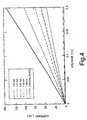
- the resistance of the PCM element 10 as a function of the programming currentis plotted in Figure 4 , showing the current versus voltage plot in seven different conditions, from a completely crystalline memory element 3 (curve with continuous line) to the completely resetted memory element 3 (abscissa line). From Figure 4 it is clear that, if the PCM element 10 is read at a reading voltage of 0,2 V, very different current values are obtained, which can be discriminated very easily and rapidly by a reading stage.
- Figure 5shows an implementation of the structure of Figures 3a-3d in a phase change memory cell of the lance type, as described for example in EP-A-1 675 183 , wherein the thin resistive region 11 has been introduced.
- Figure 5shows a phase change memory cell including a first dielectric layer 39 (preferably, USG -Undoped Silicate Glass-) extending on a semiconductor substrate which is not shown and accommodates access or selector elements, in a per se known manner.
- First-level plugs or contacts 41a and 41bextend through the first dielectric layer 39 and comprise, e.g., a barrier layer, e.g. a multiple Ti/TiN layer, and a tungsten filler.
- First-level plugs 41a and 41bare connected to two terminals of the access element, e.g. the emitter and the base regions of a bipolar junction transistor or the source and gate regions of a MOS transistor, in a per se known manner.
- a nitride layer 45 and a second dielectric layer 46extend on the first dielectric layer 39; an opening 47 extends in the second dielectric layer 46 and in the nitride layer 45 on top of the first-level plug 41a; a spacer 48 of silicon nitride coats the walls of the opening 40 and surrounds the heater 2.
- the stack 49forms a bit line running perpendicularly to the plane of Figure 5 and forming a contact with the heater 2 having a sub-lithographic dimension by virtue of the sub-lithographic width of the heater.
- the stack 49is laterally and upwardly sealed by a sealing layer 51, e.g. of nitride, extending also at the interface between the second dielectric layer 46 and a third dielectric layer 52.
- a first hole 55extends through the third dielectric layer 52 and a second hole 56 extends through the second and the third dielectric layers 46, 52.
- the holes 55, 56are coated with a barrier layer and filled by a metal layer, e.g. of Cu, to form second-level plugs 57 and 58 which are in contact with the stack 9 and the first-level plug 41b, respectively.
- the heatermay be formed by depositing the nitride layer 45, depositing the second dielectric layer 46, digging an opening in the layers 45 and 46, depositing a spacer layer and removing it from the bottom of the opening, filling the opening with a heating layer and removing the excess heating layer and spacer by CMP ("Chemical Mechanical Polishing").
- CMPChemical Mechanical Polishing
- the stack 49is formed by depositing, in sequence, a resistive layer, e.g. of TiN, TiAlN, TiSiN, a GST layer and a metal layer, and defining these three layers using a same mask. Thereafter, the sealing layer 51 is deposited.
- the heateris cup-shaped and the drawings shows only a vertical wall thereof extending over the first-level plug 41a.
- a spacer layer, a heater layer, a sheath layer and the second dielectric layerare deposited; and the wafer is planarized.
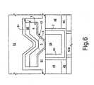
- Figure 6shows an implementation of the structure of Figures 3a-3d in a phase change memory cell of the tapered microtrench type, as described for example in US 2005/0142863 , wherein the thin resistive region 11 has been introduced.
- the heater 2is formed by a cup-shaped region formed in an opening extending in the second dielectric layer 46 and in the nitride layer 45 above and in contact with the first-level plug 41a.
- the cup-shaped regionfrom above, has a ring-like or an elongated shape (e.g., rectangular or oval) and is internally surrounded by sealing region 60, e.g. of nitride, and a filling region 59, e.g. of USG.
- a mold layer 61e.g. of nitride, extends over the second dielectric layer 46 and forms a microtrench 62 having inclined walls and tapered profile.
- the microtrench 62may be formed by plasma etch using the process described in US 2005/0142863 .
- the microtrench 62has a sublithographic bottom width and a lithographic top width.
- the stack 49may form a bit line running perpendicularly to the plane of Figure 6 and has a sublithograhic dimension in the horizontal direction.
- the stack 49has a dot-like shape, and a bitline of metal contacts the stack 49.
- a further sealing layer 51surrounds the stack 49.
- the chalcogenic region 3makes a sub-lithographic contact with the heater 2 since the heater 2 has a sub-lithographic thickness in one direction (perpendicular to the drawing plane, at the contact area) and the stack has a sub-lithographic dimension in the horizontal direction of the drawing.
- the advantages of the present inventionare clear from the above description.
- the presence of a parallel current path whose resistance depends upon the dimensions of the amorphous region 5allows a better control of the programmed resistance.
- multilevel storagemay be obtained, wherein the various bit stored in a same memory cell are associated with resistance values that can be programmed with high accuracy and easily discriminated.
- the sensingis simpler, faster and highly reliable.
- the use of a parallel resistive pathallows the use of an amorphous region or spot of suitable dimensions, thus improving the resistance stability of the programmed phase with time.
- the solutionis very simple and requires only the deposition of an extra layer with respect to standard processes, both in the lance and in the microtrench architectures; thus the invention does not increase the costs for manufacturing the memory cell or for its operation.
- System 500may be used in wireless devices such as, for example, a personal digital assistant (PDA), a laptop or portable computer with wireless capability, a web tablet, a wireless telephone, a pager, an instant messaging device, a digital music player, a digital camera, or other devices that may be adapted to transmit and/or receive information wirelessly.
- PDApersonal digital assistant
- System 500may be used in any of the following systems: a wireless local area network (WLAN) system, a wireless personal area network (WPAN) system, a cellular network, although the scope of the present invention is not limited in this respect.
- WLANwireless local area network
- WPANwireless personal area network
- cellular networkalthough the scope of the present invention is not limited in this respect.
- System 500includes a controller 510, an input/output (I/O) device 520 (e.g. a keypad, display), static random access memory (SRAM) 560, a memory 530, and a wireless interface 540 coupled to each other via a bus 550.
- I/Oinput/output
- SRAMstatic random access memory
- a battery 580is used in some embodiments. It should be noted that the scope of the present invention is not limited to embodiments having any or all of these components.
- Controller 510comprises, for example, one or more microprocessors, digital signal processors, microcontrollers, or the like.
- Memory 530may be used to store messages transmitted to or by system 500. Memory 530 may also optionally be used to store instructions that are executed by controller 510 during the operation of system 500, and may be used to store user data.
- Memory 530may be provided by one or more different types of memory.
- memory 530may comprise any type of random access memory, a volatile memory, a non-volatile memory such as a flash memory and includes the phase change memory device according to Figures 3a-3d .
- I/O device 520may be used by a user to generate a message.
- System 500uses wireless interface 540 to transmit and receive messages to and from a wireless communication network with a radio frequency (RF) signal.
- RFradio frequency
- Examples of wireless interface 540may include an antenna or a wireless transceiver, although the scope of the present invention is not limited in this respect.
- the thin resistive region 11is described as being a separate region from the heater 2, formed by an own deposition step, it may be formed by the same material of the heater, by stopping the CMP just before reaching the second dielectric layer so as to form a thin resistive layer that is then patterned by an own etching step or during patterning of the stack 49.
- the thin resistive region 11may be considered a projecting portion of the heater 2.
Landscapes
- Chemical & Material Sciences (AREA)
- Crystallography & Structural Chemistry (AREA)
- Engineering & Computer Science (AREA)
- Computer Hardware Design (AREA)
- Semiconductor Memories (AREA)
Description
- The present invention relates to a phase change memory device for multibit storage.
- As is known, phase change memory devices use phase change materials, i.e., materials that may be electrically switched between a generally amorphous and a generally crystalline state or between different detectable states of local order across the entire spectrum between completely amorphous and completely crystalline states, for electronic memory application. The state of the phase change materials is also non-volatile in that, when set in either a crystalline, semi-crystalline, amorphous, or semi-amorphous state representing a resistance value, that value is retained until changed by another programming event, as that value represents a phase or physical state of the material (e.g., crystalline or amorphous). The state is unaffected by removing electrical power.
- At present, alloys of group VI of the periodic table, such as Te or Se, referred to as chalcogenides or chalcogenic materials, can advantageously be used in phase change cells as phase change materials. The most promising chalcogenide is formed by a Ge, Sb and Te alloy (Ge2Sb2Te5), also called GST, which is currently widely used for storing information in overwritable disks.
- In chalcogenides, the resistivity varies by two or more magnitude orders when the material passes from the amorphous phase (more resistive) to the polycrystalline phase (more conductive) and vice versa.
- Phase change may be obtained by locally increasing the temperature. Below 150°C all phases are stable. Above 200°C (temperature of start of nucleation), fast nucleation of the crystallites takes place, and, if the material is kept at the crystallization temperature for a sufficient length of time, it changes its phase and becomes crystalline (so-called set state). To bring the chalcogenide back into the amorphous state (reset state), it is necessary to raise the temperature above the melting temperature (approximately 600°C) and then to cool the chalcogenide off rapidly. Intermediate phases may be obtained applying suitable temperatures for different times, which cause the formation of amorphous "spots" or "bubbles" of different dimensions in contact with the heater.
- From the electrical standpoint, it is possible to cause the chalcogenic material to change state by causing a current to flow through a resistive element, called a heater, which heats the chalcogenic material by the Joule effect.
- The basic structure of a PCM element 1 which operates according to the principles described above is shown in
Figure 1 and comprises aheater element 2 and amemory element 3 of chalcogenic material. A portion of the memory element 3 (generally polycrystalline) is in direct contact with theheater 2 and is subject to phase change between amorphous and polycrystalline.Figure 1 shows a PCM element in an intermediate state, wherein the portion that has not changed phase and enables a good flow of current is referred to aspolycrystalline portion 4 and the portion that has changed state is referred to asamorphous portion 5. The dimensions of theamorphous portion 5 define the overall resistivity of thememory region 3 and thus of the PCM element 1. Thus, different resistance levels may be associated with different bits and may be obtained by generating appropriate program currents that cause theamorphous portion 5 to assume different dimensions. - A critical issue in the multilevel programming resides in the discrimination among the different programmed states within a reasonable time.
- For a better understanding of this problem, reference is made to
Figures 2a-2d , showing a portion of the PCM element 1 ofFigure 1 in different programming conditions, obtained using progressively higher programming currents. InFigures 2a-2d , the same reference numbers have been used as inFigure 1 , whilenumber 6 represents a dielectric layer surrounding theheater 2. - As visible in
Figures 2a-2d , theamorphous portions 5 have different dimensions (radiuses). In detail, inFigure 2a , where a lower programming current was used (e.g., ip = 1.32 mA), thephase change portion 5 extends just a little beyond the edge of theheater 2, while inFigures 2b, 2c, 2d (obtained e.g. using programming currents ip = 1.42 mA, 1.51 mA and 1.6 mA, respectively) the protruding portion of thephase change portion 5 is gradually bigger. - Although the dimensions of
amorphous portions 5 are quite different in the four Figures, the difference in the resistance of the PCM element 1 inFigures 2a-2d does not change to the same extent. In fact, the current path from theheater 2 to thepolycrystalline portion 4 passes through the high resistiveamorphous portion 5; therefore the current path resistance is very high in all four conditions. Thus, the difference in resistance among the four conditions is small, compared with its absolute value, and the discrimination among the different states may be problematic, or the reading time may be unacceptably increased. - On the other hand, if a thin amorphous portion or a plurality of nanoportions are used, to obtain lower resistance values, the amorphous portion or portions is/are less stable in temperature and more subject to a resistance drift that causes reading errors.
- Moreover, the programmed resistance is entirely associated to the high resistivity of the amorphized portion. It follows that the time-dependent resistivity variation usually observed for the amorphous portion directly affects the resistance of the cell, thus impacting the reading capability of intermediate levels.
- In other words, ease and speed in reading are difficult to obtain without impairing stability in temperature and time.
- The aim of the invention is thus to provide a phase change memory device having an improved behavior.
- According to the present invention, there are provided a phase change memory device and a fabrication method thereof, as defined respectively in claims 1 and 13.
- For the understanding of the present invention, preferred embodiments thereof are now described, purely as non-limitative examples, with reference to the enclosed drawings, wherein:
Figure 1 shows the basic structure of a known phase change memory element;Figures 2a-2d show a portion of the phase change memory element ofFigure 1 in different programming conditions;Figures 3a-3d show a portion of a phase change memory element according to a schematical representation of the present phase change memory device in different programming conditions;Figure 4 shows a representation of the current vs. voltage plot for the phase change memory element according toFigure 3a-3d ;Figure 5 shows a cross-section of a phase change memory element according to an embodiment of the invention;Figure 6 shows a cross-section of a phase change memory element according to another embodiment of the invention; andFigure 7 is a system depiction for another embodiment of the invention.Figures 3a-3d show a portion of aPCM element 10 including aheater 2 surrounded by adielectric layer 6 and overlaid by amemory element 3, analogously to the PCM element 1 ofFigures 1, 2a-2d . InFigures 3a-3d , thememory element 3 has been programmed in four different conditions and includes apolycrystalline portion 4 and anamorphous portion 5, analogously toFigures 1, 2a-2d . Here, a thinresistive region 11 protrudes from the top edge of theheater 2 along the interface between thedielectric layer 6 and thememory element 3. The thinresistive region 11 is of a conductive material, e.g. metal or doped polysilicon, and has a reduced thickness. Preferably, the thinresistive region 11 is of the same material as theheater 2, for example TiN, TiAlN, TiSiN. In the alternative, it may be of a different material. For example, theheater 2 may be of TiAlN and the thinresistive region 11 is of TiSiN, or vice versa. However, other resistive materials may be used and, in general, the thinresistive region 11 may have the same, a higher or a lower resistivity than theheater 2, according to the desired resistivity and resistance differences for the various programmed states.- Furthermore, the thin
resistive region 11 has a thickness lower than 10 nm, for example comprised between 1 and 10 nm, preferably about 5 nm. - The thin
resistive region 11 forms a parallel path for a reading current flowing between theheater 2 and thepolycrystalline portion 4 of thememory element 3 and its resistance depends on the dimensions of theamorphous portion 5. In fact, a first part of the reading current flowing between theheater 2 and thepolycrystalline portion 4 flows through theamorphous portion 5 and a second part thereof flows through the thinresistive region 11. In particular, the second part of the current flows across a length of the thinresistive region 11 which is equal to the distance between the edge of theheater 2 and the edge of theamorphous portion 5. Since such a length depends on the programmed state of the PCM element 1, the parallel path has a resistance whose value depends on the programmed state of the PCM element 1. Furthermore, since the resistance of the parallel path (for a positive length of the parallel path) is much lower than the resistance of the amorphous portion, the overall resistance of the PCM element 1 depends mainly on the parallel path. Since the resistance of the parallel path depends linearly on the length thereof, the difference in resistance among the various programmed states is easily detectable by the reading circuit. - The above is clear from the comparative observation of
Figures 3a-3d , wherein theamorphous portion 5 has different dimensions according to four different programming conditions of thePCM element 10, namely obtained using progressively higher programming currents, analogously toFigures 2a-2d . - In detail, in
Figure 3a , where a lower programming current was used (e.g., ip = 1.32 mA), thephase change portion 5 extends just a little beyond the edge of theheater 2. The length X1 of the protruding portion is also the length of the parallel path. - In
Figures 3b, 3c and 3d (obtained e.g. using programming currents ip = 1.42 mA, 1.51 mA and 1.6 mA, respectively) the protruding portion of thephase change portion 5 is gradually longer. In those Figures, the lengths of the protruding portions are indicated by X2, X3 and X4. For example, assuming that X2 = 2*X1, the resistance R2 of the parallel path inFigure 3b is almost double than the resistance R1 inFigure 3a (R2 ≈ 2*R1). Analogously, assuming that X3 = 3*X1 and X4 = 4*X1, the respective resistances are R3 ≈ 3*R1 and R4 ≈ 4*R1. - The resistance of the
PCM element 10 as a function of the programming current (and thus the dimension of the amorphous portion 5) is plotted inFigure 4 , showing the current versus voltage plot in seven different conditions, from a completely crystalline memory element 3 (curve with continuous line) to the completely resetted memory element 3 (abscissa line). FromFigure 4 it is clear that, if thePCM element 10 is read at a reading voltage of 0,2 V, very different current values are obtained, which can be discriminated very easily and rapidly by a reading stage. Figure 5 shows an implementation of the structure ofFigures 3a-3d in a phase change memory cell of the lance type, as described for example inEP-A-1 675 183 , wherein the thinresistive region 11 has been introduced.- In detail,
Figure 5 shows a phase change memory cell including a first dielectric layer 39 (preferably, USG -Undoped Silicate Glass-) extending on a semiconductor substrate which is not shown and accommodates access or selector elements, in a per se known manner. First-level plugs orcontacts first dielectric layer 39 and comprise, e.g., a barrier layer, e.g. a multiple Ti/TiN layer, and a tungsten filler. First-level plugs - A
nitride layer 45 and asecond dielectric layer 46 extend on thefirst dielectric layer 39; anopening 47 extends in thesecond dielectric layer 46 and in thenitride layer 45 on top of the first-level plug 41a; aspacer 48 of silicon nitride coats the walls of the opening 40 and surrounds theheater 2. - A
stack 49 formed by the thinconductive region 11, thechalcogenic region 3 of GST (Ge2Sb2Te5), and acap region 50, of metal, extends over and in contact with theheater 2. Thestack 49 forms a bit line running perpendicularly to the plane ofFigure 5 and forming a contact with theheater 2 having a sub-lithographic dimension by virtue of the sub-lithographic width of the heater. - The
stack 49 is laterally and upwardly sealed by asealing layer 51, e.g. of nitride, extending also at the interface between thesecond dielectric layer 46 and athird dielectric layer 52. Afirst hole 55 extends through thethird dielectric layer 52 and asecond hole 56 extends through the second and the third dielectric layers 46, 52. Theholes level plug 41b, respectively. - In the cell of
Figure 5 , the heater may be formed by depositing thenitride layer 45, depositing thesecond dielectric layer 46, digging an opening in thelayers stack 49 is formed by depositing, in sequence, a resistive layer, e.g. of TiN, TiAlN, TiSiN, a GST layer and a metal layer, and defining these three layers using a same mask. Thereafter, thesealing layer 51 is deposited. - In the alternative, the heater is cup-shaped and the drawings shows only a vertical wall thereof extending over the first-
level plug 41a. In this case, after digging an opening, a spacer layer, a heater layer, a sheath layer and the second dielectric layer are deposited; and the wafer is planarized. Figure 6 shows an implementation of the structure ofFigures 3a-3d in a phase change memory cell of the tapered microtrench type, as described for example inUS 2005/0142863 , wherein the thinresistive region 11 has been introduced.- In
Figure 6 , theheater 2 is formed by a cup-shaped region formed in an opening extending in thesecond dielectric layer 46 and in thenitride layer 45 above and in contact with the first-level plug 41a. The cup-shaped region, from above, has a ring-like or an elongated shape (e.g., rectangular or oval) and is internally surrounded by sealingregion 60, e.g. of nitride, and a fillingregion 59, e.g. of USG. - A
mold layer 61, e.g. of nitride, extends over thesecond dielectric layer 46 and forms amicrotrench 62 having inclined walls and tapered profile. Themicrotrench 62 may be formed by plasma etch using the process described inUS 2005/0142863 . In particular, themicrotrench 62 has a sublithographic bottom width and a lithographic top width. - A
stack 49 formed by the thinconductive region 11, thechalcogenic region 3 of GST (Ge2Sb2Te5), and acap region 50, of metal, extends in part within themicrotrench 62 so as to contact the cup-shapedheater 2 in a plane parallel to the drawing sheet. Thestack 49 may form a bit line running perpendicularly to the plane ofFigure 6 and has a sublithograhic dimension in the horizontal direction. In the alternative, thestack 49 has a dot-like shape, and a bitline of metal contacts thestack 49. - Analogously to
figure 5 , afurther sealing layer 51 surrounds thestack 49. - Here, the
chalcogenic region 3 makes a sub-lithographic contact with theheater 2 since theheater 2 has a sub-lithographic thickness in one direction (perpendicular to the drawing plane, at the contact area) and the stack has a sub-lithographic dimension in the horizontal direction of the drawing. - The advantages of the present invention are clear from the above description. In particular, the presence of a parallel current path whose resistance depends upon the dimensions of the
amorphous region 5 allows a better control of the programmed resistance. Thus, multilevel storage may be obtained, wherein the various bit stored in a same memory cell are associated with resistance values that can be programmed with high accuracy and easily discriminated. Thus, the sensing is simpler, faster and highly reliable. - Furthermore, the use of a parallel resistive path allows the use of an amorphous region or spot of suitable dimensions, thus improving the resistance stability of the programmed phase with time.
- Moreover, since the overall resistance mainly depends on the parallel path resistivity, any modification of the resistivity of the amorphous portion on the cell resistance is negligible.
- The solution is very simple and requires only the deposition of an extra layer with respect to standard processes, both in the lance and in the microtrench architectures; thus the invention does not increase the costs for manufacturing the memory cell or for its operation.
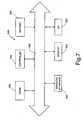
- Turning to
Figure 7 , a portion of asystem 500 in accordance with an embodiment of the present invention is described.System 500 may be used in wireless devices such as, for example, a personal digital assistant (PDA), a laptop or portable computer with wireless capability, a web tablet, a wireless telephone, a pager, an instant messaging device, a digital music player, a digital camera, or other devices that may be adapted to transmit and/or receive information wirelessly.System 500 may be used in any of the following systems: a wireless local area network (WLAN) system, a wireless personal area network (WPAN) system, a cellular network, although the scope of the present invention is not limited in this respect. System 500 includes acontroller 510, an input/output (I/O) device 520 (e.g. a keypad, display), static random access memory (SRAM) 560, amemory 530, and awireless interface 540 coupled to each other via abus 550. Abattery 580 is used in some embodiments. It should be noted that the scope of the present invention is not limited to embodiments having any or all of these components.Controller 510 comprises, for example, one or more microprocessors, digital signal processors, microcontrollers, or the like.Memory 530 may be used to store messages transmitted to or bysystem 500.Memory 530 may also optionally be used to store instructions that are executed bycontroller 510 during the operation ofsystem 500, and may be used to store user data.Memory 530 may be provided by one or more different types of memory. For example,memory 530 may comprise any type of random access memory, a volatile memory, a non-volatile memory such as a flash memory and includes the phase change memory device according toFigures 3a-3d .- I/
O device 520 may be used by a user to generate a message.System 500 useswireless interface 540 to transmit and receive messages to and from a wireless communication network with a radio frequency (RF) signal. Examples ofwireless interface 540 may include an antenna or a wireless transceiver, although the scope of the present invention is not limited in this respect. - Finally, it is clear that numerous variations and modifications may be made to the phase change memory cell and process described and illustrated herein, all falling within the scope of the invention as defined in the attached claims. For example, although the thin
resistive region 11 is described as being a separate region from theheater 2, formed by an own deposition step, it may be formed by the same material of the heater, by stopping the CMP just before reaching the second dielectric layer so as to form a thin resistive layer that is then patterned by an own etching step or during patterning of thestack 49. In this case, inFigure 5 , the thinresistive region 11 may be considered a projecting portion of theheater 2.
Claims (21)
- A phase change memory device comprising a heater element (2) and memory region (3) of chalcogenic material, the memory region having a phase changing portion (5) in electrical and thermal contact with said heater element and forming a first current path between the heater element and a rest portion (4) of said memory element, the phase changing portion having a dimension and a different resistivity from the rest portion, said dimension being correlated to information stored in said memory region,
characterised by a thin resistive region between said phase change portion (5) and a dielectric (6) to provide a parallel current path (11) between said heater element (2) and said rest portion (4) of said memory element (3). - The phase change memory device according to claim 1, wherein said parallel current path (11) has a resistance depending upon said dimension and lower than said phase changing portion (5).
- The phase change memory device according to claim 1 or 2, wherein said parallel path is a resistive region (11) extending from an upper edge of said heater (2) element, between an insulating region (6; 46, 48; 61) and said memory region (3).
- The phase change memory device according to claim 3, wherein the resistive region (11) is of a material selected between metal and polysilicon.
- The phase change memory device according to claim 3 or 4, wherein the resistive region (11) is of a same material as the heater element.
- The phase change memory device according to claim 3 or 4, wherein the resistive region (11) is of a different material from the heater element (2).
- The phase change memory device according to any of claims 3 to 6, wherein the resistive region (11) is of a material selected from TiN, TiAlN, TiSiN.
- The phase change memory device according to any of claims 3 to 6, wherein the resistive region (11) has a thickness lower than 10 nm, preferably comprised between 1 and 10 nm, most preferably of 4-5 nm.
- The phase change memory device according to any of claims 3-5 or 7, 8, wherein the resistive region (11) is a projecting portion of the heater element (2) in contact with the memory region (3).
- A phase change memory device according to any of claims 3 to 7, wherein the heater element (2) is a lance element surrounded by said insulating layer (46, 48) and the device comprises a planar memory stack (49) including said resistive region (11) and said memory region (3).
- A phase change memory device according to any of claims 3 to 7, wherein the insulating region comprises a dielectric layer (46) surrounding the heater element (2) and a mold layer (61) extending over the dielectric layer, the mold layer having a tapered microtrench (62) with has a shallower base towards the heater element (2) and a memory stack (49) extends at least in part in said tapered microtrench and includes said resistive region (11) and said memory region (3).
- A system comprising:a processor (510);a static random access memory (560) coupled to said processor; anda memory (530) coupled to said processor, the memory comprising the phase change memory device (10) according to any of claims 1-11.
- A process for manufacturing a phase change memory device comprising forming a heater element (2) and forming a memory region (3) of chalcogenic material in electrical and thermal contact with the heater element, the memory region having a phase changing portion (5) towards the heater element forming a first current path between the heater element and a rest portion (4) of said memory element, the phase changing portion having a dimension and a different resistivity from a rest portion, said dimension being correlated to information stored in said memory region,
characterised by forming a thin resistive region between said phase change portion (5) and a dielectric (6) to provide a parallel current path (11) between said heater element (2) and said rest portion (4) of said memory element. - The process according to claim 13, wherein forming a parallel current path comprises, before forming said memory region, forming a resistive region (11) over an insulating region (6; 46, 48) surrounding the heater element (2) and extending from an upper edge of said heater element.
- The process according to claim 14, wherein the phase change portion (5) has a higher resistivity than said rest portion (4) and the resistive region (11) has a lower resistivity than the phase changing portion (5).
- The process according to claim 14 or 15, wherein the resistive region (11) is of a material selected between metal and polysilicon.
- The process according to any of claims 14-16, wherein the resistive region (11) is of a same material as the heater element.
- The process according to any of claims 14 to 17, wherein the resistive region (11) is of a material selected from TiN, TiAlN, TiSiN.
- The process according to any of claims 14 to 18, wherein the resistive region (11) has a thickness lower than 10 nm, preferably comprised between 1 and 10 nm, most preferably of 4-5 nm.
- The process according to any of claims 14 to 19, wherein forming the heater element (2) comprises forming the insulating layer (6; 46, 48); forming an opening in the insulating layer; depositing a heater layer (2) in the opening; removing an excess heater layer outside the opening to have a planarized surface; depositing a layer stack (49) including a resistive layer (11) and a chalcogenic layer (3); patterning the layer stack in a same patterning step to form a memory stack (49) including the memory region (3) and the resistive region (11).
- A process according to any of claims 14 to 20, wherein forming the heater element (2) comprises forming the insulating layer (46); forming an opening in the insulating layer; depositing a heater layer (2) in the opening; removing an excess heater layer outside the opening to have a planarized surface; depositing a mold layer (61) over the planarized surface; forming, in the mold layer, a tapered aperture (62) having a shallower base in contact with the heater element; depositing a layer stack (49) including a resistive layer (11) and a chalcogenic layer (3); patterning the layer stack (49) in a same patterning step to form a memory stack including the memory region (3) and the resistive region (11) having a least one portion in the tapered aperture.
Priority Applications (7)
| Application Number | Priority Date | Filing Date | Title |
|---|---|---|---|
| DE602007010624TDE602007010624D1 (en) | 2007-09-07 | 2007-09-07 | Phase change memory device for multi-bit storage |
| EP07425555AEP2034536B1 (en) | 2007-09-07 | 2007-09-07 | Phase change memory device for multibit storage |
| DE102008041810ADE102008041810A1 (en) | 2007-09-07 | 2008-09-04 | Phase change memory device for multi-bit storage |
| TW097134288ATWI419322B (en) | 2007-09-07 | 2008-09-05 | Phase change memory device for multibit storage |
| CN200810212331.6ACN101442103B (en) | 2007-09-07 | 2008-09-08 | Phase-change memory devices for multi-bit storage |
| KR1020080088382AKR101534500B1 (en) | 2007-09-07 | 2008-09-08 | Phase change memory device for multi-bit storage |
| JP2008261125AJP5613868B2 (en) | 2007-09-07 | 2008-09-08 | Phase change memory device for multi-bit storage |
Applications Claiming Priority (1)
| Application Number | Priority Date | Filing Date | Title |
|---|---|---|---|
| EP07425555AEP2034536B1 (en) | 2007-09-07 | 2007-09-07 | Phase change memory device for multibit storage |
Publications (2)
| Publication Number | Publication Date |
|---|---|
| EP2034536A1 EP2034536A1 (en) | 2009-03-11 |
| EP2034536B1true EP2034536B1 (en) | 2010-11-17 |
Family
ID=38859091
Family Applications (1)
| Application Number | Title | Priority Date | Filing Date |
|---|---|---|---|
| EP07425555AActiveEP2034536B1 (en) | 2007-09-07 | 2007-09-07 | Phase change memory device for multibit storage |
Country Status (6)
| Country | Link |
|---|---|
| EP (1) | EP2034536B1 (en) |
| JP (1) | JP5613868B2 (en) |
| KR (1) | KR101534500B1 (en) |
| CN (1) | CN101442103B (en) |
| DE (2) | DE602007010624D1 (en) |
| TW (1) | TWI419322B (en) |
Cited By (6)
| Publication number | Priority date | Publication date | Assignee | Title |
|---|---|---|---|---|
| US11456415B2 (en) | 2020-12-08 | 2022-09-27 | International Business Machines Corporation | Phase change memory cell with a wrap around and ring type of electrode contact and a projection liner |
| US11476418B2 (en) | 2020-12-08 | 2022-10-18 | International Business Machines Corporation | Phase change memory cell with a projection liner |
| US20230085288A1 (en)* | 2021-09-13 | 2023-03-16 | International Business Machines Corporation | Electrically insulated projection liner for ai device |
| US20230105007A1 (en)* | 2021-10-04 | 2023-04-06 | International Business Machines Corporation | Artificial intelligence (ai) devices with improved thermal stability and scaling behavior |
| IT202200001130A1 (en) | 2022-01-24 | 2023-07-24 | St Microelectronics Srl | PHASE CHANGE MEMORY CELL WITH ASYMMETRIC STRUCTURE, MEMORY DEVICE INCLUDING THE PHASE CHANGE MEMORY CELL, AND METHOD FOR MANUFACTURING THE PHASE CHANGE MEMORY CELL |
| US12364174B2 (en) | 2021-12-08 | 2025-07-15 | International Business Machines Corporation | Global heater for phase change memory |
Families Citing this family (18)
| Publication number | Priority date | Publication date | Assignee | Title |
|---|---|---|---|---|
| EP3159333B1 (en) | 2007-08-08 | 2020-04-22 | Universal Display Corporation | Benzo-fused thiophene or furan compounds comprising a triphenylene group |
| US8830722B2 (en) | 2011-08-25 | 2014-09-09 | Micron Technology, Inc. | Methods, apparatuses, and circuits for programming a memory device |
| US8988926B2 (en) | 2013-01-11 | 2015-03-24 | Micron Technology, Inc. | Method, system and device for phase change memory with shunt |
| GB2515100A (en) | 2013-06-14 | 2014-12-17 | Ibm | Phase-change memory cells |
| GB2515101A (en) | 2013-06-14 | 2014-12-17 | Ibm | Phase-change memory cells |
| GB2515567A (en)* | 2013-06-28 | 2014-12-31 | Ibm | Phase-Change memory cells |
| KR20150043759A (en)* | 2013-10-15 | 2015-04-23 | 에스케이하이닉스 주식회사 | Resistance variable memory apparatus and manufacturing method thereof |
| US9853229B2 (en) | 2013-10-23 | 2017-12-26 | University Of Southern California | Organic electroluminescent materials and devices |
| IT201900021606A1 (en) | 2019-11-19 | 2021-05-19 | St Microelectronics Srl | PHASE CHANGE MEMORY DEVICE AND METHOD OF PROGRAMMING A PHASE CHANGE MEMORY DEVICE |
| US11283015B2 (en) | 2020-03-24 | 2022-03-22 | International Business Machines Corporation | Projected phase change memory devices |
| US11805711B2 (en)* | 2020-09-28 | 2023-10-31 | International Business Machines Corporation | Phase-change memory (PCM) including liner reducing resistance drift |
| US11665985B2 (en)* | 2020-11-23 | 2023-05-30 | International Business Machines Corporation | Projected memory device with reduced minimum conductance state |
| US11653578B2 (en) | 2020-12-01 | 2023-05-16 | International Business Machines Corporation | Phase-change material-based XOR logic gates |
| US11621394B2 (en)* | 2020-12-29 | 2023-04-04 | International Business Machines Corporation | Multi-layer phase change memory device |
| US11545624B2 (en) | 2021-03-29 | 2023-01-03 | International Business Machines Corporation | Phase change memory cell resistive liner |
| US20230093604A1 (en)* | 2021-09-21 | 2023-03-23 | International Business Machines Corporation | Phase-change memory with embedded air gap |
| US20230098562A1 (en)* | 2021-09-29 | 2023-03-30 | International Business Machines Corporation | Phase change memory cell sidewall projection liner |
| CN116490058A (en)* | 2022-01-24 | 2023-07-25 | 意法半导体股份有限公司 | Phase change memory cell, memory device, and corresponding methods |
Family Cites Families (14)
| Publication number | Priority date | Publication date | Assignee | Title |
|---|---|---|---|---|
| US5166758A (en)* | 1991-01-18 | 1992-11-24 | Energy Conversion Devices, Inc. | Electrically erasable phase change memory |
| US5406509A (en)* | 1991-01-18 | 1995-04-11 | Energy Conversion Devices, Inc. | Electrically erasable, directly overwritable, multibit single cell memory elements and arrays fabricated therefrom |
| US6764894B2 (en)* | 2001-08-31 | 2004-07-20 | Ovonyx, Inc. | Elevated pore phase-change memory |
| US6507061B1 (en)* | 2001-08-31 | 2003-01-14 | Intel Corporation | Multiple layer phase-change memory |
| KR100504698B1 (en)* | 2003-04-02 | 2005-08-02 | 삼성전자주식회사 | Phase change memory device and method for forming the same |
| EP1557875A1 (en) | 2003-12-29 | 2005-07-27 | STMicroelectronics S.r.l. | Process for forming tapered trenches in a dielectric material |
| KR100568511B1 (en)* | 2003-12-30 | 2006-04-07 | 삼성전자주식회사 | Semiconductor Devices Having Phase Transition Film Patterns and Manufacturing Methods Thereof |
| EP1675183A1 (en) | 2004-12-21 | 2006-06-28 | STMicroelectronics S.r.l. | Phase change memory cell with diode junction selection and manufacturing method thereof |
| US7488968B2 (en)* | 2005-05-05 | 2009-02-10 | Ovonyx, Inc. | Multilevel phase change memory |
| KR100794654B1 (en)* | 2005-07-06 | 2008-01-14 | 삼성전자주식회사 | Phase change memory device and its programming method |
| TWI290369B (en)* | 2005-07-08 | 2007-11-21 | Ind Tech Res Inst | Phase change memory with adjustable resistance ratio and fabricating method thereof |
| DE602005011972D1 (en)* | 2005-09-14 | 2009-02-05 | St Microelectronics Srl | Annular heater for a phase change memory device |
| JP2007165710A (en)* | 2005-12-15 | 2007-06-28 | Elpida Memory Inc | Method of manufacturing nonvolatile memory element |
| JP4691454B2 (en)* | 2006-02-25 | 2011-06-01 | エルピーダメモリ株式会社 | Phase change memory device and manufacturing method thereof |
- 2007
- 2007-09-07EPEP07425555Apatent/EP2034536B1/enactiveActive
- 2007-09-07DEDE602007010624Tpatent/DE602007010624D1/enactiveActive
- 2008
- 2008-09-04DEDE102008041810Apatent/DE102008041810A1/ennot_activeWithdrawn
- 2008-09-05TWTW097134288Apatent/TWI419322B/enactive
- 2008-09-08KRKR1020080088382Apatent/KR101534500B1/enactiveActive
- 2008-09-08JPJP2008261125Apatent/JP5613868B2/enactiveActive
- 2008-09-08CNCN200810212331.6Apatent/CN101442103B/enactiveActive
Cited By (7)
| Publication number | Priority date | Publication date | Assignee | Title |
|---|---|---|---|---|
| US11456415B2 (en) | 2020-12-08 | 2022-09-27 | International Business Machines Corporation | Phase change memory cell with a wrap around and ring type of electrode contact and a projection liner |
| US11476418B2 (en) | 2020-12-08 | 2022-10-18 | International Business Machines Corporation | Phase change memory cell with a projection liner |
| US20230085288A1 (en)* | 2021-09-13 | 2023-03-16 | International Business Machines Corporation | Electrically insulated projection liner for ai device |
| US20230105007A1 (en)* | 2021-10-04 | 2023-04-06 | International Business Machines Corporation | Artificial intelligence (ai) devices with improved thermal stability and scaling behavior |
| US12364174B2 (en) | 2021-12-08 | 2025-07-15 | International Business Machines Corporation | Global heater for phase change memory |
| IT202200001130A1 (en) | 2022-01-24 | 2023-07-24 | St Microelectronics Srl | PHASE CHANGE MEMORY CELL WITH ASYMMETRIC STRUCTURE, MEMORY DEVICE INCLUDING THE PHASE CHANGE MEMORY CELL, AND METHOD FOR MANUFACTURING THE PHASE CHANGE MEMORY CELL |
| EP4216698A1 (en) | 2022-01-24 | 2023-07-26 | STMicroelectronics S.r.l. | A phase-change memory cell with asymmetric structure, a memory device including the phase-change memory cell, and a method for manufacturing the phase-change memory cell |
Also Published As
| Publication number | Publication date |
|---|---|
| KR20090027152A (en) | 2009-03-16 |
| DE102008041810A1 (en) | 2009-04-16 |
| CN101442103B (en) | 2014-02-19 |
| DE602007010624D1 (en) | 2010-12-30 |
| EP2034536A1 (en) | 2009-03-11 |
| KR101534500B1 (en) | 2015-07-06 |
| JP5613868B2 (en) | 2014-10-29 |
| TWI419322B (en) | 2013-12-11 |
| JP2009071314A (en) | 2009-04-02 |
| TW200939467A (en) | 2009-09-16 |
| CN101442103A (en) | 2009-05-27 |
Similar Documents
| Publication | Publication Date | Title |
|---|---|---|
| EP2034536B1 (en) | Phase change memory device for multibit storage | |
| KR101486984B1 (en) | Variable resistance memory device and method of forming the same | |
| US8404514B2 (en) | Fabricating current-confining structures in phase change memory switch cells | |
| EP1729355B1 (en) | Self-aligned process for manufacturing phase change memory cells | |
| US8377741B2 (en) | Self-heating phase change memory cell architecture | |
| KR100808365B1 (en) | Shapinhg a phase change layer in a phase change memory cell | |
| US8796101B2 (en) | Memory device | |
| KR100766504B1 (en) | Semiconductor device and manufacturing method thereof | |
| KR100668825B1 (en) | Phase change memory device and manufacturing method thereof | |
| CN101529595B (en) | Self-aligned planar phase-change memory element and device, system using same and method of forming same | |
| US20080029752A1 (en) | Phase change memory and manufacturing method thereof | |
| US8476612B2 (en) | Method for forming a lateral phase change memory element | |
| US20090161406A1 (en) | Non-volatile memory and method for fabricating the same | |
| US7485559B2 (en) | Semiconductor device and method of fabricating the same | |
| US7985693B2 (en) | Method of producing phase change memory device | |
| US20060098524A1 (en) | Forming planarized semiconductor structures | |
| KR100968448B1 (en) | Phase change memory device and manufacturing method thereof | |
| KR20100037726A (en) | Phase change random access memory having encapsulator and method of manufacturing the same |
Legal Events
| Date | Code | Title | Description |
|---|---|---|---|
| PUAI | Public reference made under article 153(3) epc to a published international application that has entered the european phase | Free format text:ORIGINAL CODE: 0009012 | |
| AK | Designated contracting states | Kind code of ref document:A1 Designated state(s):AT BE BG CH CY CZ DE DK EE ES FI FR GB GR HU IE IS IT LI LT LU LV MC MT NL PL PT RO SE SI SK TR | |
| AX | Request for extension of the european patent | Extension state:AL BA HR MK RS | |
| 17P | Request for examination filed | Effective date:20090624 | |
| 17Q | First examination report despatched | Effective date:20090722 | |
| AKX | Designation fees paid | Designated state(s):DE | |
| RAP1 | Party data changed (applicant data changed or rights of an application transferred) | Owner name:POLITECNICO DI MILANO Owner name:STMICROELECTRONICS SRL | |
| GRAP | Despatch of communication of intention to grant a patent | Free format text:ORIGINAL CODE: EPIDOSNIGR1 | |
| GRAS | Grant fee paid | Free format text:ORIGINAL CODE: EPIDOSNIGR3 | |
| GRAA | (expected) grant | Free format text:ORIGINAL CODE: 0009210 | |
| AK | Designated contracting states | Kind code of ref document:B1 Designated state(s):DE | |
| REF | Corresponds to: | Ref document number:602007010624 Country of ref document:DE Date of ref document:20101230 Kind code of ref document:P | |
| PLBE | No opposition filed within time limit | Free format text:ORIGINAL CODE: 0009261 | |
| STAA | Information on the status of an ep patent application or granted ep patent | Free format text:STATUS: NO OPPOSITION FILED WITHIN TIME LIMIT | |
| 26N | No opposition filed | Effective date:20110818 | |
| REG | Reference to a national code | Ref country code:DE Ref legal event code:R097 Ref document number:602007010624 Country of ref document:DE Effective date:20110818 | |
| REG | Reference to a national code | Ref country code:DE Ref legal event code:R082 Ref document number:602007010624 Country of ref document:DE Representative=s name:HOEGER, STELLRECHT & PARTNER PATENTANWAELTE MB, DE | |
| REG | Reference to a national code | Ref country code:DE Ref legal event code:R079 Ref document number:602007010624 Country of ref document:DE Free format text:PREVIOUS MAIN CLASS: H01L0045000000 Ipc:H10N0070000000 | |
| PGFP | Annual fee paid to national office [announced via postgrant information from national office to epo] | Ref country code:DE Payment date:20240926 Year of fee payment:18 |