EP2004063B1 - Ultrasonic matching layer and transducer - Google Patents
Ultrasonic matching layer and transducerDownload PDFInfo
- Publication number
- EP2004063B1 EP2004063B1EP07752028.6AEP07752028AEP2004063B1EP 2004063 B1EP2004063 B1EP 2004063B1EP 07752028 AEP07752028 AEP 07752028AEP 2004063 B1EP2004063 B1EP 2004063B1
- Authority
- EP
- European Patent Office
- Prior art keywords
- layer
- matching layer
- matching
- lens
- mhz
- Prior art date
- Legal status (The legal status is an assumption and is not a legal conclusion. Google has not performed a legal analysis and makes no representation as to the accuracy of the status listed.)
- Active
Links
- 239000004593EpoxySubstances0.000claimsdescription85
- 229920001651CyanoacrylatePolymers0.000claimsdescription65
- MWCLLHOVUTZFKS-UHFFFAOYSA-NMethyl cyanoacrylateChemical compoundCOC(=O)C(=C)C#NMWCLLHOVUTZFKS-UHFFFAOYSA-N0.000claimsdescription64
- 238000002604ultrasonographyMethods0.000claimsdescription42
- 239000000463materialSubstances0.000claimsdescription36
- 238000000034methodMethods0.000claimsdescription33
- 230000008569processEffects0.000claimsdescription16
- XLYOFNOQVPJJNP-UHFFFAOYSA-NwaterSubstancesOXLYOFNOQVPJJNP-UHFFFAOYSA-N0.000claimsdescription12
- 125000006850spacer groupChemical group0.000claimsdescription10
- 230000005540biological transmissionEffects0.000claimsdescription7
- 239000003292glueSubstances0.000claimsdescription5
- 238000009736wettingMethods0.000claimsdescription5
- 239000011888foilSubstances0.000claimsdescription4
- FYYHWMGAXLPEAU-UHFFFAOYSA-NMagnesiumChemical compound[Mg]FYYHWMGAXLPEAU-UHFFFAOYSA-N0.000claims1
- 239000005030aluminium foilSubstances0.000claims1
- 239000011777magnesiumSubstances0.000claims1
- 229910052749magnesiumInorganic materials0.000claims1
- 239000010410layerSubstances0.000description350
- 239000002245particleSubstances0.000description127
- 239000002105nanoparticleSubstances0.000description45
- 239000002131composite materialSubstances0.000description36
- 239000000843powderSubstances0.000description28
- 239000013078crystalSubstances0.000description27
- 239000011159matrix materialSubstances0.000description23
- 239000000203mixtureSubstances0.000description23
- 241001465754MetazoaSpecies0.000description22
- 238000003384imaging methodMethods0.000description20
- GQYHUHYESMUTHG-UHFFFAOYSA-Nlithium niobateChemical compound[Li+].[O-][Nb](=O)=OGQYHUHYESMUTHG-UHFFFAOYSA-N0.000description17
- 238000013461designMethods0.000description15
- WFKWXMTUELFFGS-UHFFFAOYSA-NtungstenChemical compound[W]WFKWXMTUELFFGS-UHFFFAOYSA-N0.000description15
- 241000700159RattusSpecies0.000description14
- 230000035945sensitivityEffects0.000description12
- 238000004519manufacturing processMethods0.000description11
- 229910052721tungstenInorganic materials0.000description11
- 230000009974thixotropic effectEffects0.000description10
- 239000010937tungstenSubstances0.000description10
- 238000010171animal modelMethods0.000description9
- PCHJSUWPFVWCPO-UHFFFAOYSA-NgoldChemical compound[Au]PCHJSUWPFVWCPO-UHFFFAOYSA-N0.000description7
- 229910052737goldInorganic materials0.000description7
- 239000010931goldSubstances0.000description7
- 241000699666Mus <mouse, genus>Species0.000description6
- YXFVVABEGXRONW-UHFFFAOYSA-NTolueneChemical compoundCC1=CC=CC=C1YXFVVABEGXRONW-UHFFFAOYSA-N0.000description6
- 238000010586diagramMethods0.000description6
- 239000006187pillSubstances0.000description6
- 239000000853adhesiveSubstances0.000description5
- 230000001070adhesive effectEffects0.000description5
- 239000011859microparticleSubstances0.000description5
- 229920000642polymerPolymers0.000description5
- 230000008901benefitEffects0.000description4
- 125000003700epoxy groupChemical group0.000description4
- BASFCYQUMIYNBI-UHFFFAOYSA-NplatinumChemical compound[Pt]BASFCYQUMIYNBI-UHFFFAOYSA-N0.000description4
- 229920000647polyepoxidePolymers0.000description4
- 239000004926polymethyl methacrylateSubstances0.000description4
- KFZMGEQAYNKOFK-UHFFFAOYSA-NIsopropanolChemical compoundCC(C)OKFZMGEQAYNKOFK-UHFFFAOYSA-N0.000description3
- PNEYBMLMFCGWSK-UHFFFAOYSA-Naluminium oxideInorganic materials[O-2].[O-2].[O-2].[Al+3].[Al+3]PNEYBMLMFCGWSK-UHFFFAOYSA-N0.000description3
- 230000000694effectsEffects0.000description3
- 230000006870functionEffects0.000description3
- 238000011068loading methodMethods0.000description3
- 230000005499meniscusEffects0.000description3
- 238000002156mixingMethods0.000description3
- 238000012986modificationMethods0.000description3
- 230000004048modificationEffects0.000description3
- 238000010172mouse modelMethods0.000description3
- 210000000056organAnatomy0.000description3
- 238000002360preparation methodMethods0.000description3
- 230000009467reductionEffects0.000description3
- 238000011160researchMethods0.000description3
- 239000000523sampleSubstances0.000description3
- 238000003892spreadingMethods0.000description3
- 230000007480spreadingEffects0.000description3
- 238000012360testing methodMethods0.000description3
- 230000007704transitionEffects0.000description3
- CSCPPACGZOOCGX-UHFFFAOYSA-NAcetoneChemical compoundCC(C)=OCSCPPACGZOOCGX-UHFFFAOYSA-N0.000description2
- 241000283973Oryctolagus cuniculusSpecies0.000description2
- 241000283984RodentiaSpecies0.000description2
- XUIMIQQOPSSXEZ-UHFFFAOYSA-NSiliconChemical compound[Si]XUIMIQQOPSSXEZ-UHFFFAOYSA-N0.000description2
- 230000006978adaptationEffects0.000description2
- 229910052782aluminiumInorganic materials0.000description2
- XAGFODPZIPBFFR-UHFFFAOYSA-NaluminiumChemical compound[Al]XAGFODPZIPBFFR-UHFFFAOYSA-N0.000description2
- 239000011324beadSubstances0.000description2
- 230000009286beneficial effectEffects0.000description2
- 239000000919ceramicSubstances0.000description2
- 239000004020conductorSubstances0.000description2
- 238000013016dampingMethods0.000description2
- 230000001627detrimental effectEffects0.000description2
- 230000002500effect on skinEffects0.000description2
- 238000011049fillingMethods0.000description2
- 239000012212insulatorSubstances0.000description2
- 229910052751metalInorganic materials0.000description2
- 239000002184metalSubstances0.000description2
- 229910052697platinumInorganic materials0.000description2
- 229920003229poly(methyl methacrylate)Polymers0.000description2
- 229920000098polyolefinPolymers0.000description2
- 239000012254powdered materialSubstances0.000description2
- 238000012545processingMethods0.000description2
- 238000011552rat modelMethods0.000description2
- 238000007789sealingMethods0.000description2
- 229910052710siliconInorganic materials0.000description2
- 239000010703siliconSubstances0.000description2
- 238000004544sputter depositionMethods0.000description2
- 229920001169thermoplasticPolymers0.000description2
- 239000004416thermosoftening plasticSubstances0.000description2
- 238000012285ultrasound imagingMethods0.000description2
- 241000251468ActinopterygiiSpecies0.000description1
- 229920003319Araldite®Polymers0.000description1
- 241000282472Canis lupus familiarisSpecies0.000description1
- 241000700198CaviaSpecies0.000description1
- RYGMFSIKBFXOCR-UHFFFAOYSA-NCopperChemical compound[Cu]RYGMFSIKBFXOCR-UHFFFAOYSA-N0.000description1
- 241000282326Felis catusSpecies0.000description1
- 229910000846In alloyInorganic materials0.000description1
- 229920004142LEXAN™Polymers0.000description1
- 239000004418LexanSubstances0.000description1
- WHXSMMKQMYFTQS-UHFFFAOYSA-NLithiumChemical compound[Li]WHXSMMKQMYFTQS-UHFFFAOYSA-N0.000description1
- 229920005479Lucite®Polymers0.000description1
- 241000699670Mus sp.Species0.000description1
- 244000137852Petrea volubilisSpecies0.000description1
- 229920005372Plexiglas®Polymers0.000description1
- 239000004697PolyetherimideSubstances0.000description1
- 239000004793PolystyreneSubstances0.000description1
- 241000288906PrimatesSpecies0.000description1
- BQCADISMDOOEFD-UHFFFAOYSA-NSilverChemical compound[Ag]BQCADISMDOOEFD-UHFFFAOYSA-N0.000description1
- ATJFFYVFTNAWJD-UHFFFAOYSA-NTinChemical compound[Sn]ATJFFYVFTNAWJD-UHFFFAOYSA-N0.000description1
- 229920004738ULTEM®Polymers0.000description1
- 229920004747ULTEM® 1000Polymers0.000description1
- 238000005299abrasionMethods0.000description1
- NIXOWILDQLNWCW-UHFFFAOYSA-Nacrylic acid groupChemical groupC(C=C)(=O)ONIXOWILDQLNWCW-UHFFFAOYSA-N0.000description1
- 230000009471actionEffects0.000description1
- 239000002318adhesion promoterSubstances0.000description1
- 239000012790adhesive layerSubstances0.000description1
- 238000013019agitationMethods0.000description1
- 230000003444anaesthetic effectEffects0.000description1
- 230000000712assemblyEffects0.000description1
- 238000000429assemblyMethods0.000description1
- 230000036772blood pressureEffects0.000description1
- 230000000747cardiac effectEffects0.000description1
- 210000000748cardiovascular systemAnatomy0.000description1
- 229910010293ceramic materialInorganic materials0.000description1
- 239000003795chemical substances by applicationSubstances0.000description1
- 229910052804chromiumInorganic materials0.000description1
- 238000004140cleaningMethods0.000description1
- 239000002361compostSubstances0.000description1
- 150000001875compoundsChemical class0.000description1
- 238000010276constructionMethods0.000description1
- 238000001816coolingMethods0.000description1
- 230000002596correlated effectEffects0.000description1
- 230000000875corresponding effectEffects0.000description1
- 230000008878couplingEffects0.000description1
- 238000010168coupling processMethods0.000description1
- 238000005859coupling reactionMethods0.000description1
- 125000004093cyano groupChemical group*C#N0.000description1
- 238000007872degassingMethods0.000description1
- 230000032798delaminationEffects0.000description1
- 238000000151depositionMethods0.000description1
- 230000008021depositionEffects0.000description1
- 239000003599detergentSubstances0.000description1
- 238000002059diagnostic imagingMethods0.000description1
- 238000009826distributionMethods0.000description1
- 239000002019doping agentSubstances0.000description1
- -1e.g.Polymers0.000description1
- 229920001971elastomerPolymers0.000description1
- 210000002257embryonic structureAnatomy0.000description1
- 230000007613environmental effectEffects0.000description1
- 238000005530etchingMethods0.000description1
- 210000003754fetusAnatomy0.000description1
- 230000005484gravityEffects0.000description1
- 229910052738indiumInorganic materials0.000description1
- APFVFJFRJDLVQX-UHFFFAOYSA-Nindium atomChemical compound[In]APFVFJFRJDLVQX-UHFFFAOYSA-N0.000description1
- 239000000976inkSubstances0.000description1
- 238000003780insertionMethods0.000description1
- 230000037431insertionEffects0.000description1
- 230000003993interactionEffects0.000description1
- 239000007788liquidSubstances0.000description1
- 229910052744lithiumInorganic materials0.000description1
- 150000002739metalsChemical class0.000description1
- 239000004570mortar (masonry)Substances0.000description1
- 229910052759nickelInorganic materials0.000description1
- 239000003921oilSubstances0.000description1
- 230000008520organizationEffects0.000description1
- 230000035515penetrationEffects0.000description1
- 238000011170pharmaceutical developmentMethods0.000description1
- 230000000704physical effectEffects0.000description1
- 239000004033plasticSubstances0.000description1
- 229920003023plasticPolymers0.000description1
- 239000004417polycarbonateSubstances0.000description1
- 229920000515polycarbonatePolymers0.000description1
- 229920001601polyetherimidePolymers0.000description1
- 239000004848polyfunctional curativeSubstances0.000description1
- 229920000306polymethylpentenePolymers0.000description1
- 239000011116polymethylpenteneSubstances0.000description1
- 229920002223polystyrenePolymers0.000description1
- 238000011417postcuringMethods0.000description1
- 229920005989resinPolymers0.000description1
- 239000011347resinSubstances0.000description1
- 230000029058respiratory gaseous exchangeEffects0.000description1
- 230000004044responseEffects0.000description1
- 230000000630rising effectEffects0.000description1
- 239000004576sandSubstances0.000description1
- 229920002379silicone rubberPolymers0.000description1
- 239000004945silicone rubberSubstances0.000description1
- 229910052709silverInorganic materials0.000description1
- 239000004332silverSubstances0.000description1
- 125000003808silyl groupChemical group[H][Si]([H])([H])[*]0.000description1
- 239000000758substrateSubstances0.000description1
- 229920001187thermosetting polymerPolymers0.000description1
- 229910052718tinInorganic materials0.000description1
- 239000011800void materialSubstances0.000description1
- 230000003245working effectEffects0.000description1
Images


Classifications
- B—PERFORMING OPERATIONS; TRANSPORTING
- B06—GENERATING OR TRANSMITTING MECHANICAL VIBRATIONS IN GENERAL
- B06B—METHODS OR APPARATUS FOR GENERATING OR TRANSMITTING MECHANICAL VIBRATIONS OF INFRASONIC, SONIC, OR ULTRASONIC FREQUENCY, e.g. FOR PERFORMING MECHANICAL WORK IN GENERAL
- B06B3/00—Methods or apparatus specially adapted for transmitting mechanical vibrations of infrasonic, sonic, or ultrasonic frequency
- B—PERFORMING OPERATIONS; TRANSPORTING
- B06—GENERATING OR TRANSMITTING MECHANICAL VIBRATIONS IN GENERAL
- B06B—METHODS OR APPARATUS FOR GENERATING OR TRANSMITTING MECHANICAL VIBRATIONS OF INFRASONIC, SONIC, OR ULTRASONIC FREQUENCY, e.g. FOR PERFORMING MECHANICAL WORK IN GENERAL
- B06B1/00—Methods or apparatus for generating mechanical vibrations of infrasonic, sonic, or ultrasonic frequency
- B06B1/02—Methods or apparatus for generating mechanical vibrations of infrasonic, sonic, or ultrasonic frequency making use of electrical energy
- B06B1/06—Methods or apparatus for generating mechanical vibrations of infrasonic, sonic, or ultrasonic frequency making use of electrical energy operating with piezoelectric effect or with electrostriction
- B06B1/0644—Methods or apparatus for generating mechanical vibrations of infrasonic, sonic, or ultrasonic frequency making use of electrical energy operating with piezoelectric effect or with electrostriction using a single piezoelectric element
- B06B1/0662—Methods or apparatus for generating mechanical vibrations of infrasonic, sonic, or ultrasonic frequency making use of electrical energy operating with piezoelectric effect or with electrostriction using a single piezoelectric element with an electrode on the sensitive surface
- B06B1/067—Methods or apparatus for generating mechanical vibrations of infrasonic, sonic, or ultrasonic frequency making use of electrical energy operating with piezoelectric effect or with electrostriction using a single piezoelectric element with an electrode on the sensitive surface which is used as, or combined with, an impedance matching layer
- B—PERFORMING OPERATIONS; TRANSPORTING
- B32—LAYERED PRODUCTS
- B32B—LAYERED PRODUCTS, i.e. PRODUCTS BUILT-UP OF STRATA OF FLAT OR NON-FLAT, e.g. CELLULAR OR HONEYCOMB, FORM
- B32B7/00—Layered products characterised by the relation between layers; Layered products characterised by the relative orientation of features between layers, or by the relative values of a measurable parameter between layers, i.e. products comprising layers having different physical, chemical or physicochemical properties; Layered products characterised by the interconnection of layers
- B32B7/04—Interconnection of layers
- B32B7/12—Interconnection of layers using interposed adhesives or interposed materials with bonding properties
- G—PHYSICS
- G10—MUSICAL INSTRUMENTS; ACOUSTICS
- G10K—SOUND-PRODUCING DEVICES; METHODS OR DEVICES FOR PROTECTING AGAINST, OR FOR DAMPING, NOISE OR OTHER ACOUSTIC WAVES IN GENERAL; ACOUSTICS NOT OTHERWISE PROVIDED FOR
- G10K11/00—Methods or devices for transmitting, conducting or directing sound in general; Methods or devices for protecting against, or for damping, noise or other acoustic waves in general
- G10K11/02—Mechanical acoustic impedances; Impedance matching, e.g. by horns; Acoustic resonators
- G—PHYSICS
- G10—MUSICAL INSTRUMENTS; ACOUSTICS
- G10K—SOUND-PRODUCING DEVICES; METHODS OR DEVICES FOR PROTECTING AGAINST, OR FOR DAMPING, NOISE OR OTHER ACOUSTIC WAVES IN GENERAL; ACOUSTICS NOT OTHERWISE PROVIDED FOR
- G10K11/00—Methods or devices for transmitting, conducting or directing sound in general; Methods or devices for protecting against, or for damping, noise or other acoustic waves in general
- G10K11/18—Methods or devices for transmitting, conducting or directing sound
- G10K11/26—Sound-focusing or directing, e.g. scanning
- G10K11/30—Sound-focusing or directing, e.g. scanning using refraction, e.g. acoustic lenses
- G—PHYSICS
- G10—MUSICAL INSTRUMENTS; ACOUSTICS
- G10K—SOUND-PRODUCING DEVICES; METHODS OR DEVICES FOR PROTECTING AGAINST, OR FOR DAMPING, NOISE OR OTHER ACOUSTIC WAVES IN GENERAL; ACOUSTICS NOT OTHERWISE PROVIDED FOR
- G10K9/00—Devices in which sound is produced by vibrating a diaphragm or analogous element, e.g. fog horns, vehicle hooters or buzzers
- G10K9/12—Devices in which sound is produced by vibrating a diaphragm or analogous element, e.g. fog horns, vehicle hooters or buzzers electrically operated
- G10K9/122—Devices in which sound is produced by vibrating a diaphragm or analogous element, e.g. fog horns, vehicle hooters or buzzers electrically operated using piezoelectric driving means
- H—ELECTRICITY
- H10—SEMICONDUCTOR DEVICES; ELECTRIC SOLID-STATE DEVICES NOT OTHERWISE PROVIDED FOR
- H10N—ELECTRIC SOLID-STATE DEVICES NOT OTHERWISE PROVIDED FOR
- H10N30/00—Piezoelectric or electrostrictive devices
- H10N30/50—Piezoelectric or electrostrictive devices having a stacked or multilayer structure
- A—HUMAN NECESSITIES
- A61—MEDICAL OR VETERINARY SCIENCE; HYGIENE
- A61B—DIAGNOSIS; SURGERY; IDENTIFICATION
- A61B8/00—Diagnosis using ultrasonic, sonic or infrasonic waves
- A61B8/42—Details of probe positioning or probe attachment to the patient
- A61B8/4209—Details of probe positioning or probe attachment to the patient by using holders, e.g. positioning frames
- Y—GENERAL TAGGING OF NEW TECHNOLOGICAL DEVELOPMENTS; GENERAL TAGGING OF CROSS-SECTIONAL TECHNOLOGIES SPANNING OVER SEVERAL SECTIONS OF THE IPC; TECHNICAL SUBJECTS COVERED BY FORMER USPC CROSS-REFERENCE ART COLLECTIONS [XRACs] AND DIGESTS
- Y10—TECHNICAL SUBJECTS COVERED BY FORMER USPC
- Y10T—TECHNICAL SUBJECTS COVERED BY FORMER US CLASSIFICATION
- Y10T156/00—Adhesive bonding and miscellaneous chemical manufacture
- Y10T156/10—Methods of surface bonding and/or assembly therefor
- Y—GENERAL TAGGING OF NEW TECHNOLOGICAL DEVELOPMENTS; GENERAL TAGGING OF CROSS-SECTIONAL TECHNOLOGIES SPANNING OVER SEVERAL SECTIONS OF THE IPC; TECHNICAL SUBJECTS COVERED BY FORMER USPC CROSS-REFERENCE ART COLLECTIONS [XRACs] AND DIGESTS
- Y10—TECHNICAL SUBJECTS COVERED BY FORMER USPC
- Y10T—TECHNICAL SUBJECTS COVERED BY FORMER US CLASSIFICATION
- Y10T428/00—Stock material or miscellaneous articles
- Y10T428/31504—Composite [nonstructural laminate]
- Y10T428/31855—Of addition polymer from unsaturated monomers
Definitions
- Small animal imagingis an important field of research in many areas including preclinical pharmaceutical development, developmental biology, cardiac research, and molecular biology.
- Several small animal modelsare widely used in theses fields, the most prevalent being the mouse and the rat.
- High frequency ultrasoundhas been widely used to image the mouse model at frequencies from about 20 megahertz (MHz) to over 60 MHz.
- the rat modelis difficult to image at high frequencies in comparison to the mouse because the rat has highly attenuating and echogenic epidermal, dermal, and sub-dermal tissues.
- JP-A-2001 069594discloses an ultrasound probe comprising a piezoelectric device, a sound matching layer laminated to the piezoelectric device, and a lens laminated to the sound matching layer via an adhesion agent layer.
- the lenscomprises silicone rubber
- the adhesion layerpreferably comprises silyl group polymer adhesives, but could instead comprise cyano adhesive.
- US-A-2002/0111620discloses a lens for an ultrasound probe comprising TPX.
- an ultrasonic transducer stackcomprising a plurality of stacked layers, the plurality of stacked layers comprising: a piezoelectric layer; a first matching layer; and a lens layer, wherein each layer of the plurality of layers has a top surface and an opposed bottom surface; wherein the first matching layer is connected to and underlies the bottom surface of the lens layer, and wherein the piezoelectric layer underlies the bottom surface of the matching layer, characterised in that the first matching layer comprises cyanoacrylate and is configured to be about a 1 ⁇ 4 acoustic wavelength matching layer; and in that the lens layer comprises TPX.
- a process for producing an ultrasonic transducer stackcomprising a plurality of layers, each layer having a top surface and an opposed bottom surface, the process comprising: providing a piezoelectric layer; providing a lens layer; bonding a first matching layer to the bottom surface of the lens layer; and positioning the bonded first matching layer and lens layer into substantial overlying registration with the piezoelectric layer to produce an ultrasonic transducer stack, characterised in that the lens layer comprises TPX, and in that the first matching layer comprises cyanoacrylate and is configured to be a 1 ⁇ 4 wavelength matching layer.
- Rangescan be expressed herein as from “about” one particular value, and/or to "about” another particular value. When such a range is expressed, another aspect includes from the one particular value and/or to the other particular value. Similarly, when values are expressed as approximations, by use of the antecedent "about,” it will be understood that the particular value forms another aspect. It will be further understood that the endpoints of each of the ranges are significant both in relation to the other endpoint, and independently of the other endpoint.
- the terms "optional” or “optionally”mean that the subsequently described event or circumstance may or may not occur, and that the description includes instances where said event or circumstance occurs and instances where it does not.
- subj ectan individual.
- the term subj ectincludes small or laboratory animals as well as primates, including humans.
- a laboratory animalincludes, but is not limited to, a rodent such as a mouse or a rat.
- the term laboratory animalis also used interchangeably with animal, small animal, small laboratory animal, or subject, which includes mice, rats, cats, dogs, fish, rabbits, guinea pigs, rodents, etc.
- laboratory animaldoes not denote a particular age or sex. Thus, adult and newborn animals, as well as fetuses (including embryos), whether male or female, are included.
- the present inventionis directed to matching layers for ultrasonic transducer stacks having a plurality of layers.
- Ultrasound transducers, or transducer stacks, that are used for imagingutilize acoustic matching layers positioned between a piezoelectric layer and a lens layer or face layer of the transducer.
- the piezoelectric layertypically has a high acoustic impedance (Z).
- the subject being imagedtypically has a much lower acoustic impedance. If the piezoelectric layer were pressed directly onto the subject, a great deal of the acoustic energy would be lost due to the impedance mismatch between the piezoelectric layer and the subject.
- matching layers with acoustic impedances between the piezoelectric layer and the lens or face layerare introduced into the transducer stack to provide a transition from the higher impedance piezoelectric layer to the lower impedance subject.
- the matching layers provided hereincan be used in an ultrasonic transducer stack to accomplish an impedance transition from a piezoelectric layer to a lens or face layer.
- the exemplary matching layerscan have varying acoustic impedances.
- One exemplary matching layercan have an acoustic impedance of between about 7.0 MegaRayles and about 14.0 MegaRayles.
- Another exemplary matching layercan have an acoustic impedance of between about 3.0 MegaRayles and about 7.0 MegaRayles.
- Yet another exemplary matching layercan have an acoustic impedance of between about 2.5 MegaRayles and about 2.8 MegaRayles.
- each exemplary matching layercan be a 1 ⁇ 4 wavelength matching layer.
- An ultrasonic transducer stackcan be used to generate, transmit and receive ultrasound of high frequency (equal to or greater than 20 megahertz).
- Exemplary ultrasonic transducer stackscomprise at least one disclosed matching layer.
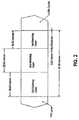
- FIG. 1shows a transducer stack 100 having a lithium nibate piezoelectric layer 102.
- the bottom surface of the piezoelectric layeroverlies the top surface of a backing layer 104.
- Above the top layer of the piezoelectric layerare an electrode layer 106, three exemplary matching layers (108, 110 and 112), an epoxy bonding layer 114, and a lens layer 116.
- the matching layer 108is a higher impedance matching layer that can have an acoustic impedance of between about 7.0 MegaRayles and about 14.0 MegaRayles.
- the matching layer 108can comprise nano and micron sized particles as described below.
- the matching layer 110Above the upper surface of the matching layer 108 is the matching layer 110, which has a lower impedance that the matching layer 108.
- the matching layer 110can have an acoustic impedance of between about 3.0 MegaRayles and about 7.0 MegaRayles.
- the matching layer 110can comprise light and heavy particles as described below.
- the matching layer 112has a lower impedance than the matching layer 110.
- the matching layer 112has an acoustic impedance of between about 2.5 MegaRayles and about 2.8 MegaRayles.
- the matching layer 112can comprise cyanoacrylate as described below.
- the matching layer 112can be bonded to the underlying matching layer 110 using a layer of epoxy 114.
- the face layer of the exemplary transducer stack 100comprises a lens layer 116.
- the lens layercan comprise TPX as described below.
- the lens layer 116can be directly bonded to the matching layer 112.
- the matching layersaccomplish an impedance transition from a piezoelectric layer 102 to a lens layer 116.
- a transducer stackcan be used to image subjects, or anatomical portions thereof, using high frequency ultrasound.
- the images producedcan have a high resolution.
- an ultrasonic transducer stackcomprises a plurality of layers, each layer having a top surface and an opposed bottom surface.
- the plurality of layersincludes a piezoelectric layer and at least one matching layer. When positioned in a transducer stack, the bottom surface of a given matching layer overlies the top surface of the piezoelectric layer.
- a matching layercan comprise a composite material.
- the composite materialcan comprise a matrix material loaded with a plurality of micron-sized and nano-sized particles.
- the composite materialcan also comprise a matrix material loaded with a plurality of first heavy particles and a plurality of second light particles.
- a matching layercan also comprise cyanoacrylate (CA).
- Capturing of ultrasound data using an exemplary transducer stackcomprises generating ultrasound, transmitting ultrasound into the subject, and receiving ultrasound reflected by the subject.
- a wide range of frequencies of ultrasoundcan be used to capture ultrasound data.
- clinical frequency ultrasoundless than 20 MHz
- high frequency ultrasoundequal to or greater than 20 MHz
- One skilled in the artcan readily determine what frequency to use based on factors such as, for example, but not limited to, depth of imaging, or desired resolution.
- High frequency ultrasoundmay be desired when high resolution imaging is desired and the structures to be imaged within the subject are not at too great a depth.
- capturing ultrasound datacan comprise transmitting ultrasound having a frequency of at least 20MHz into the subject and receiving a portion of the transmitted ultrasound that is reflected by the subject.
- a transducer having a center frequency of about 20MHz, 30MHz, 40MHz, 50MHz, 60MHz or highercan be used.
- the transducercan have a center frequency of about 20 MHz (for a design frequency of 25 MHz per the general frequency example given herein below.).
- High frequency ultrasound transmissionis often desirable for the imaging of small animals, where a high resolution may be achieved with an acceptable depth of penetration.
- the methodscan therefore be used at clinical or high frequency on a small animal subject
- the small animalcan be a rat or mouse.
- the disclosed transducerscan be operatively connected to an ultrasound imaging system for the generation, transmission, receipt, and processing of ultrasound data.
- ultrasoundcan be transmitted, received and processed using an ultrasonic scanning device that can supply an ultrasonic signal of at least about 20 MHz to the highest practical frequency. Any ultrasound system or device capable of operating at 20 MHz or above can be used.
- the matching layers described hereincan be used with other devices capable of transmitting and receiving ultrasound at the desired frequencies.
- ultrasound systems using arrayed transducerscan be used.
- a small animal subjectcan exemplarily be positioned on a platform with access to anesthetic equipment.
- the methodscan be used with platforms and apparatus used in imaging small animals including "rail guide” type platforms with maneuverable probe holder apparatuses.
- the described systemscan be used with multi-rail imaging systems, and with small animal mount assemblies as described in U.S. Patent Application No. 10/683,168 , entitled “Integrated Multi-Rail Imaging System,” U.S. Patent Application No. 10/053,748 , entitled “Integrated Multi-Rail Imaging System,” U.S. Patent Application No. 10/683,870 , now U.S. Patent No. 6,851,392, issued February 8, 2005 , entitled “Small Animal Mount Assembly," and U.S. Patent Application No. 11/053,653 , entitled “Small Animal Mount Assembly”.
- the systemcan include means for acquiring ECG and temperature signals for processing and display.
- the systemcan also display physiological waveforms such as an ECG, respiration or blood pressure waveform.
- the disclosed system for producing an ultrasound image using line based image reconstructioncan provide an ultrasound image having an effective frame rate in excess of 200 frames per second.
- the systemcomprises an ECG based technique that enables high time resolution and allows the accurate depiction of a rapidly moving structure, such as a heart, in a small animal, such as a mouse, rat, rabbit, or other small animal, using ultrasound.
- a heartor a portion thereof, can be imaged using the methods and systems described herein.
- the methods and systemsare not limited to imaging the heart, however, and it is contemplated that other organs or portions thereof, including other portions of the cardiovascular system can be imaged.
- Exemplary operational characteristics that overcome these imaging obstaclescan comprise high sensitivity to overcome attenuation, a matched lens system to overcome reverb, and/or the use of a matched attenuation layer between the transducer and the tissue to attenuate multiple reflections.
- the transducer described for imaging the ratcan have a broad bandwidth, so as not to compromise axial resolution.
- a transducer incorporating an acoustic match to water, sensitivity, and broad bandwidth responseis described herein and is useful for the imaging of a subject animal model.
- the transducerimproves high frequency ultrasonic imaging on rats and other small animal models.
- the transduceris relatively broadband with, for example, a -6 dB bandwidth of about 80% or greater.
- matching layers for an ultrasonic transducer stack having a plurality of layersare provided.
- the matching layer describedcan be a layer of an ultrasonic transducer stack including a piezoelectric layer.
- the stackcan comprise other layers, such as, for example and not meant to be limiting, a backing layer, other matching layers, a lens layer, a signal electrode layer, a ground electrode layer, bonding layers and/or other layers known to those skilled in the art.
- a matching layercomprises a composite material.
- the composite materialcan comprise a matrix material loaded with a plurality of micron-sized and nano-sized particles.
- the composite materialcan also comprise a matrix material loaded with a plurality of heavy and light particles.
- a matching layercan also comprise cured cyanoacrylate.
- ultrasound transducer stacksthat comprise a plurality of layers, each layer having a top surface and an opposed bottom surface.
- the plurality of layersincludes a piezoelectric layer and at least one matching layer.
- the matching layerscan be positioned in the stack such that they substantially overlie the top surface of the piezoelectric layer.
- An exemplary stackcan comprise a matching layer comprising a composite material loaded with a plurality of nano and micron sized particles, a matching layer with a plurality of heavy and light particles and a matching layer comprising cyanoacrylate.
- Piezoelectric materialsthat can be used include, for example and not meant to be limiting, ceramics, composite ceramic materials, and single crystals.
- lithium niobateLiNb
- 36 degree Y-Rotated Lithium Niobateis an exemplary material for the piezoelectric layer.
- Lithium Niobate(LiNb) has a high Q (in the region of 10,000) that can result in a narrow band transducer. It is contemplated that the high Q can be compensated for with a broad band matching structure and a damping backing system, which acts to reduce the Q of the transducer.
- a backing systemcan be used with the transducer stack and can be connected to and/or underlie the bottom side piezoelectric layer. If used, a backing layer accomplishes several things. First, it has an acoustic impedance that causes the transducer to resonate with the desired bandwidth. Secondly, it is highly attenuating so that there are reduced or no internal reflections in the transducer itself. Finally, the backing layer can be in operative contact with the piezoelectric element.
- the acoustic impedance of the backing layeris chosen as low as possible, relative to the Z of LiNb, to achieve high sensitivity while ensuring good bandwidth.
- an acoustic impedance in the range of between about 5 MR to 7 MRgives a desirable trade-off between sensitivity and bandwidth.
- a backing impedance of between about 25 MR to 40 MRcan be employed.
- the backing layercan be electrically conductive, or it can be an insulator. However, whether a conductor or insulator is used, the backing layer is operatively connected to the piezoelectric layer.
- the conductive backing layercan result in a faster manufacturing process, with a very narrow range of possible attenuation and acoustic impedances available.
- the non-conductive backing layerallows for a very wide range of damping and attenuation possibilities.
- One exemplary backing layeris formed from Ablebond 16-1 conductive epoxy.
- This backing layer materialhas an acoustic impedance of about 6.7 MR and an attenuation of over about 100 dB/mm at 30 MHz.
- this exemplary conductive epoxyexhibits excellent conductivity at the bond line and makes an integral connection with the piezoelectric layer.
- metalscan also be used to form the backing layer such as, for example and not meant to be limiting, indium, tin, and alloys of indium.
- a lens layercan also be used.
- a lens that is substantially acoustically matched to watercan be used.
- Such a lenscan have a speed of sound either higher or lower than that of water, but sufficiently different from water so that a practical curvature can be realized to achieve a desired amount of focusing.
- An exemplary lens material that can be usedis polymethylpentene or TPX. This thermoplastic has an acoustic impedance of 1.8 MR and a longitudinal velocity of 2200 m/s.
- a convex lens(one with a speed of sound lower than water) can also be used.
- TPXis lossy compared to some other alternatives (5.7 dB/mm at 30 MHz), but provides an exceptionally good acoustic match to water and tissue.
- the primary challenge in using TPXis that it is very difficult to bond to other layers of the ultrasonic transducer stack.
- Rexolitea thermo set cross linked polystyrene
- TPXhas a lower loss than TPX having a loss of only about 1.1 dB/mm at 30 MHz, but has an acoustic impedance of 2.6 MR.
- Rexolitecan be used where sensitivity is at a premium, and multiple reflections can be tolerated.
- the lens thin and the F-Number toward the higher end of the usual rangewhich is typically between about 2.5 - 3, the lossiness can be mitigated.
- an exemplary at least one 1 ⁇ 4 wavelength wave matching layeris used in the ultrasonic transducer stack.
- 1 ⁇ 4 wavelength matching layersare also known simply as “matching layers.”
- matching layeris used throughout the description of the present invention and has the same meaning as 1 ⁇ 4 wave or wavelength matching layer.
- the 1 ⁇ 4 wave matching layerinfluences both sensitivity, and bandwidth.
- matching layerscan be on the order of between about 5.0 um to over 50.0 ⁇ m thick, and there is typically a low tolerance for intermediate adhesive layers. For example, a layer of more than 500 nm can be detrimental to the design, and anything over 1500 nm can substantially negate the effect of the stack.
- the thicknessdepends on the desired transmit frequency and the speed of sound in the layer. One of skill in the art could thus readily determine the appropriate thickness for a 1 ⁇ 4 wavelength for a matching layer comprising heavy and light particles through routine testing for the speed of sound of the composite and knowledge of the desired design frequency.
- the exemplary lens layercomprises TPX that is connected to a cyanoacrylate matching layer, which has an acoustic impedance of approximately 3 MR.
- the cyanoacrylate matching layeris bonded to the TPX lens layer for attachment to other layers of the stack.
- an approximately 10 MR matching layeris overlaid on a matching layer having an impedance between about 4.5 - 5 MR to enhance the bandwidth and maintain excellent sensitivity.
- Thiscan exemplarily be accomplished using two layers of tungsten doped epoxy that are sanded to a desired thickness using a vacuum sander.
- the lower impedance layercan also be doped with SiC nano-particles to prevent settling of the tungsten powder during curing.
- another matching layercan be the cyanoacrylate (CA) layer deposited thereon the TPX lens.
- the CA matching layer, bonded to the lens layer,can be bonded with a layer of epoxy to the lower impedance matching layer, which is located in the stack underneath the bottom surface of the CA layer.
- the elevational thickness of the epoxy layeris about 5 ⁇ m thickness or less. Due to the acoustic similarity of the epoxy to the CA, at a thickness of a few microns ( ⁇ 5 um at 20 MHz) this layer is not significant to the performance of the stack.
- the epoxycan be, for example and not meant to be limiting, Epotek 301 epoxy.
- a rubber toughened CAsuch as Loctite Black Max
- a matching layer for an ultrasonic transducer stackcomprising a plurality of layers can comprise a composite material having a matrix material loaded with a plurality of micron-sized and nano-sized particles.
- the composite materialforms the matching layer of the ultrasonic transducer stack.
- the matching layercan be a 1 ⁇ 4 acoustic wavelength matching layer.
- the particlescan be of varying dimension within the respective nano and micon size domains.
- the loaded particleshave a largest lengthwise or elongate dimension that is less than the thickness of the matching layer.
- the micron-sized particleshave a largest lengthwise dimension that is about 5 um and the nano-sized particles have a largest lengthwise dimension that is about 800 nm wherein the matching layer thickness is larger than 5 um.
- the selected particlesare as small as possible without making it impossible to get to the desired acoustic impedance. Nominally, in a matching layer, attenuation should be kept to a minimum, and the particle size is much smaller than a wave length. For example, a 5 um particle in a 16.5 um quarter wave layer is approximately 1/13 of a wave length.
- the micron-sized and nano-sized particlescan comprise a high density metal.
- the micron-sized and nano-sized particlescan comprise tungsten, gold, platinum or a mixture thereof.
- high density ceramicssuch as, for example, PZT, can be used if a non-conductive layer is desired.
- the matrix materialcan be a polymer.
- the polymer forming the matrixis an epoxy.
- the epoxycan be a low viscosity, room temperature cure epoxy with a Tg above the maximum operating temperature of the transducer.
- Some non-limiting epoxy examplesinclude Epotek® 301 and 302 (Epotek, Billerica, MA), Cotronics Duralco® 4461 (Cotronics, Brooklyn, NY), West Systems Epoxies (West Systems, Bay City, MI) and various Araldite® Epoxy combinations.
- the matching layercan also be a thermoplastic such as polymethylmethacrylate (PMMA), e.g., acrylic, plexiglas, Lucite, or polycarbonate (PC), e.g., Lexan.
- PMMApolymethylmethacrylate
- PCpolycarbonate
- the micron-sized and nano-sized particlescan be loaded in the matrix material in a ratio of between about 5:1 and about 1:5 parts micron-sized particles to nano-sized particles by weight.
- the micron-sized and nano-sized particlescan be loaded in the matrix material in a ratio of between about 1:1 par micron-sized particles to nano-sized particles by weight.
- the desired percentage of large particlescan increase. For example, if a 10 MR matching layer is desired, a 1:1 ratio can be used. In another example, for a 12 MR layer, a ratio of 2:1 or 3:1 micro:nano can be used.
- the nano-sized particles and micron-sized particles of the matching layercomprise between about 10% and about 35% of the composite material on a volume basis. In other examples, the nano-sized particles and micron-sized particles can comprise between about 25% and about 30% of the composite material on a volume basis. In one preferred embodiment, the nano-sized particles and micron-sized particles comprise about 25% of the composite material on a volume basis.
- the matching layer having nano and micro particlescan be designed with a desired acoustic impedance.
- the acoustic impedance of the matching layercan be formed to be between about 7.0 MegaRayles (MR) and 14.0 MegaRayles (MR). In one preferred aspect, the acoustic impedance of the matching layer is about 10 MR.
- the matching layercan also vary in thickness.
- the thickness to achieve a 1 ⁇ 4 wavelength matching layerwill vary with the speed of sound in the matching layer and the frequency of the ultrasound passing through the matching layer.
- the speed of sound in the matching layercan be between about 1000 meters per second (m/s) and 3000 m/s.
- the elevational thickness of a matching layercan be between about 4 ⁇ m and 30 ⁇ m.
- a process for producing the nano/micron particle matching layercomprises providing a matrix material, a plurality of micron-sized particles and a plurality of nano-sized particles.
- the matrix materialis loaded with a plurality of the micron-sized particles and a plurality of the nano-sized particles to form a composite material and the formed composite material is used to produce the matching layer of an ultrasonic transducer stack.
- the micron-sized particles and the nano-sized particlescan comprise the same base material.
- the micron-sized particles and the nano-sized particlescan also be comprised of different base materials.
- the nano/micro particle matching layercan be used as a matching layer in an exemplified ultrasonic transducer stack 100 having a plurality of layers.
- the exemplary ultrasound stack 100comprises a plurality of layers, each layer having a top surface and an opposed bottom surface.
- the plurality of layersincludes a piezoelectric layer 102 and at least one matching layer.
- multiple matching layers108, 110, and 112 can be used in the transducer stack 100.
- the matching layer 108comprises the 1 ⁇ 4 wavelength acoustic matching layer described above.
- the piezoelectric layercan generate ultrasound at a center frequency of at least about 20 megahertz (MHz) for transmission through the first matching layer.
- MHzmegahertz
- the piezoelectric layercan generate ultrasound at a center frequency of at least about 20 MHz, 25 MHz, 30 MHz, 35 MHz, 40 MHz, 45 MHz, 50 MHz, 55 MHz, 60 MHz, 65 MHz, 70 MHz or higher for transmission through the first matching layer.
- the piezoelectric layercan have an acoustic impedance of 20 MR or greater.
- one exemplary type of piezoelectric layer that can be usedcomprises lithium niobate, which has an impedance of about 34 MR.
- the piezoelectric layercan comprise PZT, which has an impedance of about 33-35 MR.
- One exemplary matching layer of an ultrasonic transducer stack having a plurality of layerscomprises a composite material comprising a matrix material loaded with a plurality of first heavy particles and a plurality of second light particles.
- the light and heavy particlesare not limited in size in this embodiment.
- the matching layer comprising the light and heavy particlescan comprise a mixture of nano and micro particles.
- the light particlescan be micro sized or nano sized and the heavy particles can be micro sized or nano sized, any combination of which can be added to the matrix material.
- the matching layer having heavy and light particlescan comprise a 1 ⁇ 4 acoustic wavelength matching layer.
- the light particleshave a mass density of about 4.0 grams per cubic centimeter (g/cc) or lower and the heavy particles have a mass density of greater than about 4.0 g/cc.
- the light particlescan have a mass density of between about 2.5 g/cc and about 4.0 g/cc.
- the heavy particlescan have a mass density of, for examples, 10.0 g/cc or more.
- the first heavy particlescan comprise micron-sized or nano-sized particles selected from the group consisting of tungsten particles and lead zirconate titrate particles or a mixture thereof.
- the second light particlescomprise micron-sized or nano-sized particles selected from the group consisting of silicon carbite particles and alumina particles or a mixture thereof.
- the density of the second light particlescan be between about 100%-200% of the density of the final composite of the heavy particles and the matrix.
- the heavy and light particlescan vary in size.
- the heavy or light particlescan be less than 1 micron.
- the loaded particleshave a largest lengthwise or elongate dimension that is less than 1/50 th of a wave length in the matching layer which they comprise.
- the heavy and light particlescan be loaded in the matrix material, which can comprise a polymer such as, for example, an epoxy.
- the loaded plurality of particlescan comprise al least about 11.0% of the composite material by volume.
- the plurality of particlescan comprise between about 11.0% and about 20.0% of the composite material by volume.
- about 5.5% of the composite material by volumecomprises a plurality of nano-sized heavy particles and about 5.5 % of the composite material by volume comprises a plurality of nano-sized light particles.
- the heavy particlescan be tungsten particles, PZT particles, gold particles, or platinum particles and the light particles can be silicon carbite particles or alumina particles.
- the acoustic impedance of the matching layer comprising heavy and light particlescan vary.
- the acoustic impedance of this layercan be between about 3.0 MegaRayles and 7.0 MegaRayles. In one exemplary embodiment, the acoustic impedance is about 4.5 MR.
- the thickness of the matching layercan also vary. One skilled in the art could thus readily determine the appropriate thickness for a 1 ⁇ 4 wavelength for a matching layer comprising heavy and light particles through routine testing for the speed of sound and knowledge of the desired transmit frequency.
- the matching layercan have a speed of sound of between about 1500 m/s and about 4500 m/s. In other examples, the speed of sound in the matching layer is between about 1800 m/s and about 2500 m/s. In one preferred embodiment, the speed of sound in the matching layer is about 2100 m/s. In various aspects, it is contemplated that the thickness of the exemplified matching layer comprising heavy and light particles can be between about 4.0 microns and 30 microns.
- the matching layeris about 22.0 microns thick in the elevational dimension of the ultrasonic transducer stack.
- a process for producing the light/heavy matching layercomprises providing a matrix material, a plurality of first heavy particles and a plurality of second light particles.
- the matrix materialis loaded with a plurality of the first heavy particles and a plurality of the second light particles to form a composite material that is used as a matching layer of an ultrasonic transducer stack.
- An ultrasound transducer stackcan comprise a matching layer comprising light and heavy particles as described above.
- This matching layercan comprise a lower impedance matching layer of a transducer stack that also comprising a higher impedance matching layer.
- the higher impedance matching layercomprises nano and micro particles of similar weight and or material as the lower impedance matching layer.
- an exemplary stack 100can comprise a plurality of layers, each layer having a top surface and an opposed bottom surface.
- the plurality of layerscan include a piezoelectric layer 102 and at least one matching layer.
- a matching layer 110can comprise a composite material comprising a matrix material loaded with a plurality of first heavy particles and a plurality of second light particles, wherein the bottom surface of the matching layer 110 overlies the top surface of the piezoelectric layer 102.
- the ultrasound transducer stack 100can further comprises a matching layer 108 having a higher impedance than the impedance of the matching layer 110, the matching layer 108 being positioned between the top surface of the piezoelectric layer 102 and the bottom surface of the matching layer 110.
- the piezoelectric layercan generate ultrasound at a center frequency of at least about 20 megahertz (MHz) for transmission through one or more matching layer.
- the piezoelectric layercan generate ultrasound at a center frequency of at least about 25 MHz, 30 MHz, 35 MHz, 40 MHz, 45 MHz, 50 MHz, 55 MHz, 60 MHz, 65 MHz, 70 MHz or higher for transmission through one or more matching layer.
- the ultrasoundcan be transmitted through the matching layer 108 and then through the matching layer 110.
- a backing layer 104 of an ultrasonic transducer stack 100having a plurality of layers.
- the backing layercan comprise a composite material having a matrix material loaded with a plurality of micron-sized and nano-sized particles.
- a backing layer 104 of an ultrasonic transducer stack 100comprising a composite material having a matrix material loaded with a plurality of first heavy particles and a plurality of second light particles.
- Example 1Fabrication of an Exemplary LiNb 20-25 MHz Transducer Stack with a TPX Lens
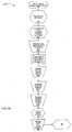
- FIG. 5is a block diagram showing an exemplary method of fabricating an exemplary LiNb 20-25 MHz transducer with a TPX lens.
- the fabrication processis described below in three exemplary sections. First, the fabrication of matching layers and piezoelectric layer to form a stack is described. Second, the fabrication of the lens layer and a cyanoacrylate matching layer is described. Finally, bonding of the lens and cyanoacrylate layer to the transducer stack is described.
- a LiNb Crystalis prepared for the piezoelectric layer as shown in block 504.
- a 36 degree Y-Cut LiNb crystalis lapped to a thickness of 0.4 lambda of the desired center frequency to compensate for mass loading.
- the crystalis plated with 3000 A of gold using a suitable means such as E-Beam deposition or Sputtering.
- a suitable meanssuch as E-Beam deposition or Sputtering.
- typically a thin layer of Cr or Nican be used to improve adhesion of the gold layer.
- the gold side of the LiNb crystalis cleaned with Acetone. After cleaning, the crystal is placed in a clean place until further handling.
- a nano-particle and micro-particle loaded epoxyis prepared for 1 ⁇ 4 wave matching layers.
- a high impedance matching layer, having an impedance above about 8 MRis prepared in block 506.
- Creating a loaded epoxy composite with acoustic impedance over 8 MRis typically limited by the maximum volumetric ratio of powder that can be wetted by the epoxy. Achieving volumetric ratios of over 20 % with particles small enough to be compatible with a 25 MHz design is challenging due to the large surface area to volume ratio of fine powders. With a 20 % volumetric limitation and using tungsten powder, it is difficult to create composites with acoustic impedances over about 8 - 9 MR. See, e.g., Martha G. Grewe, T.R.
- a low viscosity epoxy(less than 1000 cps is preferred) allows for the greatest volumetric ratio of powder to be added to the epoxy before the mixture becomes too dry to use.
- An example of such an epoxyknown in the art, is Epotek 301. See, e.g., Haifeng Wang, Tim Ritter, Wenwu Cao, and K. Kirk Shung, "Passive Materials for High Frequency Ultrasound Transducers", SPIE Conf. on Ultrasonic Transducer Engineering, San Diego, California, Feb. 1999, SPIE Vol. 3664 .
- the epoxyis mixed completely before addition of any powders.
- a volumetric ratio of 25% powder in an epoxy matrixis used.
- relatively large 5 ⁇ m particlesare used.
- a sub-micron tungsten (W) powder mixed with the 5 ⁇ m powder to a ratio of 1:1is also used. This is effective over a range of at least 1:6 to 2:1 by weight.
- the upper limit of density that can be achieved in a powder loaded epoxyis limited by the ability to wet the surface of all the powder particles. As the particle size increases, the ratio of the volume of the powdered material, to the surface area increases linearly.
- the volumetric ratio of powder to epoxy that can be sufficiently wetted to result in a void free mixtureincreases.
- the particle diametercan be small compared to the wavelength of the matrix (epoxy).
- the particle sizecan be sufficiently small that the composite contains at least 15 or more particles through its thickness.
- the exemplified use of a mixture of nano-particles with larger particlesallows for high density loaded powders with both high volumetric fractions of the loading powder and excellent control over settling. Settling is controlled by adjusting the amount of nano-particles to control the viscosity and thixotropic index of the resulting paste.
- the nano-particlesalso provide that at any given cross section, the 1 ⁇ 4 wave layer (16.5 um thick at 25 MHz for example) has a high number of particles and an even spatial distribution of powder particles ( i.e. there are no large areas of epoxy between large particles as would be the case with just large particles).
- An exemplary W doped Epoxy preparationcomprises a mixed batch of 3:1 vol. / vol. Epotek 301 epoxy to 50%:50% 5 ⁇ m: ⁇ 1 um tungsten powder. This is a highly thixotropic paste and is an 85% by weight tungsten mixture with a density of 5.7 g/cc and a volumetric fraction of 25% tungsten.
- the mixturecan be weighed out as follows: 0.5 g of mixed 301 epoxy (0.1 g of hardener and 0.4 g of resin); 1.5 g of ⁇ 1 um W powder; 1.5 g of 5 um W powder.
- a medium acoustic impedance matching layerhaving an impedance between about 3.5 MR to 6 MR is fabricated as shown in block 514 by mixing lightweight particles with heavy particles.
- the creation of medium acoustic impedance matching layerscan use high volumetric fractions of a single light particle to achieve mid and upper impedances in this range.
- using a single material, with a sufficiently small particle size to create medium acoustic impedancetypically requires a difficult search for an appropriate density material available in a suitable powder grain size.
- High volumetric fractionsmaking mixing, degassing, and spreading/application very difficult due to high viscosity and highly thixotropic pastes being created, which leads to manufacturing issues.
- the volumetric fraction of powderare typically be kept above 11% to keep attenuation low, often a compromise must be made between achieving the ideal acoustic impedance and ideal physical properties, or a new material must be sought and the process begun again.
- a solutionis possible that decouples the problem of achieving the desired acoustic impedance from the issues of viscosity, wetting, and thixotropic index.
- a heavy materialis mixed to a volumetric fraction resulting in the desired acoustic impedance, then light nano-particles are added until a desirable viscosity and thixotropic index are achieved (i.e., a paste that is easily wetted, but will not flow all over or settle.)
- a commercially available light weight nano particle of SiCmay be used as the light weight particle.
- the acoustic impedance of the matching layeris controlled almost exclusively by the volumetric faction of the heavy powder, which would have significant settling issues at that fraction.
- the viscosity and consistency of the composite mixture and settlingis controlled almost exclusively by the light weight powder.
- the light weight powderis selected so that its density is within between about 100% to 200% of the density of the desired composite density of the heavy powder-epoxy mixture.
- a 5.5% volumetric fraction of nano-particles of tungsten powderis used in a suitable room temperature cure low viscosity epoxy to achieve an acoustic impedance of between about 4.5 MR - 5 MR.
- SiC nano-particlesare then added to achieve an exemplified 11 % volumetric fraction.
- This exemplified mixtureis easy to work with, wets very well, and does not settle appreciably over a 24 hour cure period during which the epoxy to sets.
- the mixturesettles out completely in seconds, however, after the addition of the SiC, the mixture becomes thixotropic, and does not settle.
- the addition of SiC particlesminimally changes the acoustic impedance, but significantly changes the viscosity and eliminates settling of the mixture. Any desired acoustic impedance can be achieved in the medium range while maintaining a desirable working property without settling, and without needing extremely high volumetric fractions using two readily obtainable powdered materials. Also due to the size of the nano-particles, attenuation and scattering are kept to a minimum, making this an exceptional matching layer.
- the W-Doped epoxycan be added to the stack as shown in block 508.
- Application of the matching layersrequires careful attention, as air pockets in the matching layer can generally result in a malfunctioning stack. Air pockets near the interface of the piezoelectric crystal and the powder loaded epoxy can be detrimental.
- the loaded epoxyis spread evenly and air pockets are forced to the surface of the mixture.
- the thixotropic pastes used to make matching layersare difficult to 'flow' onto a part and normally require agitation to flow like a liquid.
- a vibrating manipulatorfor example, an engraver with a piece of 22 gauge wire attached to it
- the vibrationencourages air pockets to rise to the surface of the paste, where they can be sanded away. This allows the use of highly thixotropic pastes that do not settle after they have been spread as desired.
- an engraver tip modified with 22 gauge hard temper copper wire L-Shaped tipis used to move the thixotropic paste smoothly over the surface for good wetting and promotion of the rising of air pockets to the surface.
- the engraver tipis used over the entire surface of the aperture and is set to a low amplitude high frequency setting (about 7,200 spm).
- the surface of the LiNb crystalis covered leaving a small part of the rim (about .25 mm) uncovered around the edge so that it can be used for a ground later. If epoxy is placed on the rim, it cannot be cleaned effectively without removing the whole batch off the face of the transducer.
- the epoxyis allowed to cure at room temperature and post cure at an elevated temperature as shown in block 510.
- Room temperature cure epoxiesare used so that significant shrinkage of the layers, which can cause warping of the piezoelectric crystal, does not occur.
- a high Tgis preferred, so an epoxy is selected that is compatible with an elevated temperature post cure in an oven.
- the epoxyis allowed to cure at room temperature for about 18 hours or more (24 hours is preferred). Further, the cured epoxy is post cured in incubator for about 3 or more hours at 65 degrees C.
- a second lower impedance layeris fabricated and applied as shown in block 514.
- a second medium acoustic impedance pasteis applied to the first layer and the process of spreading, curing, and material removal is repeated to create the second 1 ⁇ 4 wave layer.
- a batchis mixed as follows: W powder doped epoxy using a 17:1 vol. / vol. or (51% W by weight) mixture of Epotek 301 and ⁇ 1 ⁇ m Tungsten powder. 50% of the mass of the mixture in ⁇ 1 um SiC powder is added and mixed until a smooth paste is achieved. Any lumps in the paste can be removed by mixing lightly in a mortar and pestle.
- the mixturemay be weighted out as follows: 0.5 g of mixed 301 epoxy; 0.52 g of ⁇ 1 um W powder; 0.2 g of ⁇ 1 um SiC powder.
- the second layeris applied as with the 1st, using the L-shaped tip in the engraver for even spreading of the paste, and for good wetting.
- the mixtureis allowed to cure at room temperature for about 18 - 24 hours, then post cured at 65 degrees for about 3 hours or more.
- the second matching layeris sanded and/or lapped as show in block 516.
- the support structure for the stackis prepared and the crystal is bonded to the support structure as shown in block 518 and 520.
- the stackis positioned in a housing.
- a Ultem 1000 (polyetherimide) insertcan be used having an ID matching the desired transducer aperture and height and OD matching the specifications of the desired Ti transducer housing so that the top of the insert is about 1.5 mm below the rim of the Ti housing.
- the front face of the insertis cleaned and inspected so that it is clean and free of burrs or flashing.
- the insertcan be cleaned with the ultrasonic cleaner and detergent initially and can be cleaned just before use with isopropyl alcohol.
- a small quantity of a suitable low temp cure medium viscosity epoxy(e.g. , Loctite E-20 HP) is prepared and is applied to the cleansed front face of the insert in a very thin coat using a sponge tipped swab.
- the epoxyis not applied so heavily as to form a meniscus across the wall thickness of the insert.
- the crystalis placed, with the stack side up, onto the epoxy covered face of the insert and is centered on the insert.
- the lithium niobate crystalis applied to the insert by using a vacuum pick-up tool.
- a small amount of forceis applied to push the crystal onto the face of the insert, which causes the epoxy to flow toward the edges of the underlying insert.
- the centered crystalis placed into a incubator for curing at about 40 degrees C for about 3 hours.
- the insert/crystal assemblyis inspected to ensure that the crystal is centered and completely adhered to the insert. Subsequently, the periphery of the insert/crystal assembly is cleaned. The non-increased diameter of the Ultem insert is checked by sliding the part into an exemplary housing.
- the acoustic stackcan be housed onto a suitable support structure and a rear electrode and suitably attenuating backing material can be applied as shown in blocks 522 and 524. These functions are can be combined by using conductive epoxy as a backing layer.
- the exemplified insert/crystal assemblyis normally placed in a clean smooth work surface crystal layer down.
- the back cavityis filled with Ablebond 16-1 silver conductive epoxy.
- the cavityis filled by first placing a dollop of epoxy in the center of the cavity using an epoxy syringe and applicator tip. The epoxy is applied to the entire back face of the crystal making sure not to allow any air pockets to be trapped in the backing material. The epoxy syringe is used to continue filling with the tip of the applicator below the surface of the epoxy so that no air pockets are created in the epoxy when filling.
- the cavityis filled until the conductive epoxy is about 0.5 mm below the rim of the insert.
- the backed stackcan now be housed in a suitable housing depending on the application that the device is intended for, taking into consideration, weight budgets, temperature, and RF shielding, etc. and is sealed as shown in blocks 526 and 528.
- the pillis placed onto the Housing fixture with the uncured epoxy up. Several small dots of Loctite E-20 HP are applied to the back rim of the pill such that the dots do not flow together.
- a completed housingis laid over the pill until the pill makes contact with the back of the housing.
- the fixture clampis placed over the housing to hold it in place, and allowed to cure at room temperature for about 18 hours or more.
- the assemblyis then placed into an incubator at 65 degrees for about 3 hours for post curing.
- the face of the pillis oriented parallel to the floor and pointing down to help prevent the backing layer from flowing inside the housing.
- a sealing layercan be applied.
- a bead of epoxyis applied around the perimeter of the crystal so that a continuous smooth surface exists between the crystal and the Ti housing.
- Epotek 301 epoxyis placed around the perimeter of the LiNb crystal and the inside diameter of the housing.
- the surface of the crystalis about 1.25 mm below chamfer on the Ti housing in order to desirably achieve a negative meniscus of epoxy between the crystal and the Ti housing.
- Both the crystal and the Tiare clean and free of epoxy on their surfaces so that gold can be sputtered onto both surfaces.
- a high magnification(about 20 times and preferably more) is used to place the epoxy bead.
- the epoxycan be applied at three locations around the perimeter and allowed to run around the perimeter using gravity and capillary action.
- a piece of fine gauge wire(26 gauge or so) can be attached to the end of a sharp Q-tip to improve control to help the glue to flow around the entire perimeter.
- the resultant constructis allowed to cure at room temperature for about 12 - 18 hours.
- the sealing procedurecan be repeated and the construct is allowed to cure at room temp for about 18 hours then is incubated at 65 degrees for a post cure of about 3 hours.
- the rim of the Ti housingis inspected for epoxy. Any epoxy found on the rim is removed.
- a ground connection to a signal return pathis made to the exposed gold rim of the acoustic stack as shown in block 530.
- attaching such an electrodeincluding sputtering, conductive inks and epoxies, direct mechanical contact with a good conductor, etc.
- the stackin one example, can then be bonded to a third low impedance matching layer and a lens.
- a well-matched lensis selected.
- the lensis closely matched to water in terms of acoustic impedance to provide for a reduction of reverberation artifacts.
- the lens materialcan be low in attenuation and have a speed of sound sufficiently different from water so as to be able to create a focusing effect without extreme curvature.
- many transducer designsmake use of cured piezoelectric elements, or array structures as alternatives to lenses.
- TPXa preferred lens material that has an acoustic match to water.
- TPXis a member of the polyolefin family and has a close acoustic impedance match to water and tissue compared to most plastics.
- TPXhas an acoustic impedance of between about 1.78 MR to 1.85 MR. See, e.g., Alan R. Selfridge, "Approximate Material Properties in Isotropic Materials," IEE Trans. Sonics and Ultrasonics, Vol. SU-32, No.3, May 1985 .
- TPXis difficult to bond with epoxies and most other adhesives.
- the most common use of TPX in industryis as a release film. That is, TPX is recognized as a material that most things will not stick to. While some surface preparation techniques can be used to enhance bond strength, in fact, even with adhesion promoters and primers, or coronal etching TPX is often not bondable in a demanding application and must be jointed either mechanically or heat sealed or welded. See, Timothy Ritter, K. Kirk Shung, Xuecang Geng, Pat Lopath, Richard Tutwiler, and Thomas Shrout," Proceedings of SPIE - Volume 3664 Medical Imaging 1999: Ultrasonic Transducer Engineering, K. Kirk Shung, Editor, June 1999, pp. 67-75 .
- the bondline between a lens and an acoustic stack in an imaging transducercan experience temperature swings of over 40 degrees Celsius in a few minutes, and rapid cooling routinely during use. In addition, it is constantly bombarded with ultrasonic energy. Weakness in bonding generally results in delamination and dead spots in the transducer. For this reason, high quality bond lines are desired for transducer construction.
- the lensremains in contact with the stack at all times. Even a thin disbond can result in a dead spot in the transducer.
- CA adhesive systemsare bonded to the TPX lens.
- a suitable primersuch as, for example and not meant to be limiting, Verik AC77, some toluene based primers, and the like
- CAcan form a robust bond to TPX.
- cyanoacrylate's curing characteristicsbeing very sudden and dependant on substrate and environmental conditions, CA has not been used in transducer stacks. The glue can snap cure occurs suddenly at the very thin bond lines used in making a high frequency ultrasonic stack.
- the addition of bondline spacersis often not used with CA adhesives as they cause instant curing of the material due to their large surface areas.
- CAcannot be powder loaded for the same reason, further making it an unlikely candidate for transducer manufacturing. Moreover, acoustic properties of CA have not been available in the literature, as the material cannot be cured in a thick enough section for standard testing. Furthermore, material properties that may be used to acoustically model CA have been unavailable for similar reasons.
- CAcan be cured over a narrow range of thickness.
- the range over which CA can be curedcan be used for forming 1 ⁇ 4 wave matching layers for frequencies from 5 MHz up to over 60 MHz.
- the acoustic properties of CAwere determined by using it as a matching layer and were correlated to a model using PiezoCAD software based on the KLM model available from Sonic Concepts, Woodinville, Washington USA. The results showed that CA can be used as a matching layer with acoustic impedance of between about 2.5 MR -2.8 MR.
- One exemplary method to bond TPX to a 1 ⁇ 4 wave matching systemmakes use of CA.
- the bond between the TPX layer and the CA layerwas tested and results indicated that the interface between the CA layer and TPX layer is at least as strong as the TPX itself.
- itis not suitable for bonding directly to the stack, as the bond thickness cannot be controlled, and voids and misalignment are likely, which can ruin an almost complete transponder stack at the last stages of assembly.
- a 1 ⁇ 4 wave thick cured layer of CAis created on the back (flat side) of the TPX lens layer, and the formed construct is then bonded to the upper surface of the previously formed stack with a traditional epoxy.
- the epoxybonds readily to the CA layer, and the CA layer, which is, in turn, bonded to the TPX lens layer.
- the CA layerforms a 1 ⁇ 4 wave matching layer from the top of the stack to the TPX lens layer.
- a quantity of CA gluesuch as, for example, Verik PR40, is coated onto the back of the TPX lens by means of an aluminum foil release layer and wire spacers as shown in blocks 534 and 536.
- the release filmis placed onto a flat surface (preferably a vacuum plate so that the foil is flat).
- the aluminum foilis clean and free of oil and moisture.
- Wiresare laid in a pattern onto the release film.
- the wiresare positioned in a radial pattern so that the wires do not meet at their common vertex. These wires are used as spacers for the layer of CA.
- a wire having a diameter of about 25 ⁇ mis used to form a CA layer having a resultant thickness about 23 ⁇ m - 25 ⁇ m.
- Thisis slightly thicker than the desired 1 ⁇ 4 wave thickness for CA, which would be between about 21 to 23 ⁇ m for a 25 MHz design frequency transducer.
- the longitudinal velocity in CAis between about 2100 m/s to 2200 m/s.
- the 1- 3 ⁇ m surplus materialis removed during a later abrasion process which also acts to prepare the surface of the CA layer to improve adhesion of the epoxy used to glue the lens layer having the adhered CA layer to the underlying stack.
- the back face of the TPX lens layeris abraded with a suitable grit SiC sandpaper to improve the surface for adhesion and is treated with a suitable CA polyolefin primer, such as, for example, Verik AC77, toluene based primers, and the like, as shown in block 532.
- a suitable CA polyolefin primersuch as, for example, Verik AC77, toluene based primers, and the like.
- the back of the lensis then covered with a generous amount of CA so that substantially the entire surface is wetted as shown in block 536.
- CAwill not cure quickly when allowed to form a relatively thick meniscus on the back of the lens, and so the generous amount of CA provides sufficient time to place the lens onto the prepared release film/wire arrangement.
- the lens layerwith the applied CA, is placed onto the release film and pressed lightly so that the lens "sandwiches" the wires between the underlying release film and the lens layer as shown in block 538.
- the lens and the attached release filmis removed from the vacuum plate and the release film is peeled off the lens layer as shown in block 542.
- the CA layeris allowed to cure for about 24 hours, as shown in block 540, at which time 1 - 3 ⁇ m of CA are then removed with SiC sand paper to abrade the surface of the newly formed CA layer in preparation for bonding to the stack as shown in block 544.
- the composite formed lens layer/CA layeris bonded to the transducer stack as shown in blocks 548, 550 and 552.
- a suitable low viscosity RT cure epoxysuch as Epotek 301, with an acoustic impedance value close to that of the CA layer is used to glue the composite lens layer/CA layer to the underlying stack.
- the lensis held in place using a fixture to maintain pressure of at least about 100 kPa during curing of the epoxy.
- An extended post cure at an elevated temperature using a external heat sourceis used for curing epoxy at such a thin bondline, which ensures the production of a bondline of less than 5 ⁇ m, and preferably from 1 ⁇ m - 3 ⁇ m.
- the above exemplary methodscan be used to create a transducer stack wherein the piezoelectric layer has a center frequency range of from about 5 MHz to about 60 MHz or higher.
- Such a transducercan be used to image small animals, including the rat, using high transmit frequencies (greater than or equal to 20MHz).
- Example 2General High Frequency Design for an Exemplified Broadband (85 - 95 % - 6dB bandwidth) LiNb Transducer with TPX lens
- Table 1shows the different layers that make up an exemplary transducer stack.
- the stack designcan be used for transducers with a center frequency from about 20 MHz to over 60 MHz.
- the design center frequency ⁇ Dis chosen to be higher than the desired operating center frequency of the device ⁇ O to compensate for mass loading which reduces the center frequency of a device.
- ⁇ Dis the frequency that the device would operate at in air with no lens and air backing.
Landscapes
- Engineering & Computer Science (AREA)
- Physics & Mathematics (AREA)
- Acoustics & Sound (AREA)
- Multimedia (AREA)
- Mechanical Engineering (AREA)
- Transducers For Ultrasonic Waves (AREA)
- Ultra Sonic Daignosis Equipment (AREA)
Description
- Small animal imaging is an important field of research in many areas including preclinical pharmaceutical development, developmental biology, cardiac research, and molecular biology. Several small animal models are widely used in theses fields, the most prevalent being the mouse and the rat. High frequency ultrasound has been widely used to image the mouse model at frequencies from about 20 megahertz (MHz) to over 60 MHz. The rat model, however, is difficult to image at high frequencies in comparison to the mouse because the rat has highly attenuating and echogenic epidermal, dermal, and sub-dermal tissues.
JP-A-2001 069594 US-A-2002/0111620 discloses a lens for an ultrasound probe comprising TPX.- According to a first aspect of the present invention, there is provided an ultrasonic transducer stack comprising a plurality of stacked layers, the plurality of stacked layers comprising: a piezoelectric layer; a first matching layer; and a lens layer, wherein each layer of the plurality of layers has a top surface and an opposed bottom surface; wherein the first matching layer is connected to and underlies the bottom surface of the lens layer, and wherein the piezoelectric layer underlies the bottom surface of the matching layer, characterised in that the first matching layer comprises cyanoacrylate and is configured to be about a ¼ acoustic wavelength matching layer; and in that the lens layer comprises TPX.
- According to a second aspect of the present invention, there is provided a process for producing an ultrasonic transducer stack comprising a plurality of layers, each layer having a top surface and an opposed bottom surface, the process comprising: providing a piezoelectric layer; providing a lens layer; bonding a first matching layer to the bottom surface of the lens layer; and positioning the bonded first matching layer and lens layer into substantial overlying registration with the piezoelectric layer to produce an ultrasonic transducer stack, characterised in that the lens layer comprises TPX, and in that the first matching layer comprises cyanoacrylate and is configured to be a ¼ wavelength matching layer.
- Other systems, methods, and aspects and advantages of the invention will be discussed with reference to the Figures and to the detailed description.
- The accompanying drawings, which are incorporated in and constitute a part of this specification, illustrate certain aspects of the instant invention and together with the description, serve to explain, without limitation, the principles of the invention. Like reference characters used therein indicate like parts throughout the several drawings.
FIG. 1 is a schematic diagram illustrating an exemplary transducer stack having a plurality of layers, and showing a plurality of matching layers.FIG. 2 is a schematic diagram showing a cross section of an exemplary transducer stack in the elevational dimension.FIG. 3 is a block schematic diagram illustrating an exemplary transducer stack with electrical connections.FIG. 4 is a enlarged schematic diagram illustrating layers of the exemplary transducer stack ofFig. 3 , shown in exemplary scaled dimensions.FIG. 5 is a block diagram illustrating an exemplary method of fabricating an exemplary transducer stack.- The present invention can be understood more readily by reference to the following detailed description, examples, drawings, and claims, and their previous and following description. However, before the present devices, systems, and/or methods are disclosed and described, it is to be understood that this invention is not limited to the specific devices, systems, and/or methods disclosed unless otherwise specified, as such can, of course, vary. It is also to be understood that the terminology used herein is for the purpose of describing particular aspects only and is not intended to be limiting.
- The following description of the invention is provided as an enabling teaching of the invention in its best, currently known embodiment. To this end, those skilled in the relevant art will recognize and appreciate that many changes can be made to the various aspects of the invention described herein, while still obtaining the beneficial results of the present invention. It will also be apparent that some of the desired benefits of the present invention can be obtained by selecting some of the features of the present invention without utilizing other features. Accordingly, those who work in the art will recognize that many modifications and adaptations to the present invention are possible and can even be desirable in certain circumstances and are a part of the present invention. Thus, the following description is provided as illustrative of the principles of the present invention and not in limitation thereof.
- As used herein, the singular forms "a," "an" and "the" include plural referents unless the context clearly dictates otherwise. Thus, for example, reference to a "layer" includes aspects having two or more such layers unless the context clearly indicates otherwise.
- Ranges can be expressed herein as from "about" one particular value, and/or to "about" another particular value. When such a range is expressed, another aspect includes from the one particular value and/or to the other particular value. Similarly, when values are expressed as approximations, by use of the antecedent "about," it will be understood that the particular value forms another aspect. It will be further understood that the endpoints of each of the ranges are significant both in relation to the other endpoint, and independently of the other endpoint.
- As used herein, the terms "optional" or "optionally" mean that the subsequently described event or circumstance may or may not occur, and that the description includes instances where said event or circumstance occurs and instances where it does not.
- By a "subj ect" is meant an individual. The term subj ect includes small or laboratory animals as well as primates, including humans. A laboratory animal includes, but is not limited to, a rodent such as a mouse or a rat. The term laboratory animal is also used interchangeably with animal, small animal, small laboratory animal, or subject, which includes mice, rats, cats, dogs, fish, rabbits, guinea pigs, rodents, etc. The term laboratory animal does not denote a particular age or sex. Thus, adult and newborn animals, as well as fetuses (including embryos), whether male or female, are included.
- The present invention may be understood more readily by reference to the following detailed description of preferred embodiments of the invention and the examples included therein and to the Figures and their previous and following description.
- In one embodiment, the present invention is directed to matching layers for ultrasonic transducer stacks having a plurality of layers. Ultrasound transducers, or transducer stacks, that are used for imaging utilize acoustic matching layers positioned between a piezoelectric layer and a lens layer or face layer of the transducer. The piezoelectric layer typically has a high acoustic impedance (Z). The subject being imaged typically has a much lower acoustic impedance. If the piezoelectric layer were pressed directly onto the subject, a great deal of the acoustic energy would be lost due to the impedance mismatch between the piezoelectric layer and the subject. In the ultrasound imaging arts, matching layers with acoustic impedances between the piezoelectric layer and the lens or face layer are introduced into the transducer stack to provide a transition from the higher impedance piezoelectric layer to the lower impedance subject.
- Thus, the matching layers provided herein can be used in an ultrasonic transducer stack to accomplish an impedance transition from a piezoelectric layer to a lens or face layer. The exemplary matching layers can have varying acoustic impedances. One exemplary matching layer can have an acoustic impedance of between about 7.0 MegaRayles and about 14.0 MegaRayles. Another exemplary matching layer can have an acoustic impedance of between about 3.0 MegaRayles and about 7.0 MegaRayles. Yet another exemplary matching layer can have an acoustic impedance of between about 2.5 MegaRayles and about 2.8 MegaRayles. One skilled in the art will appreciate that each exemplary matching layer can be a ¼ wavelength matching layer.
- An ultrasonic transducer stack can be used to generate, transmit and receive ultrasound of high frequency (equal to or greater than 20 megahertz). Exemplary ultrasonic transducer stacks comprise at least one disclosed matching layer.
- A schematic of such an exemplary transducer stack is shown in
FIG. 1. FIG. 1 shows atransducer stack 100 having a lithium nibatepiezoelectric layer 102. The bottom surface of the piezoelectric layer overlies the top surface of abacking layer 104. Above the top layer of the piezoelectric layer are anelectrode layer 106, three exemplary matching layers (108, 110 and 112), anepoxy bonding layer 114, and alens layer 116. - In this aspect, the
matching layer 108 is a higher impedance matching layer that can have an acoustic impedance of between about 7.0 MegaRayles and about 14.0 MegaRayles. In another aspect, thematching layer 108 can comprise nano and micron sized particles as described below. - Above the upper surface of the
matching layer 108 is thematching layer 110, which has a lower impedance that thematching layer 108. The matchinglayer 110 can have an acoustic impedance of between about 3.0 MegaRayles and about 7.0 MegaRayles. In another aspect, thematching layer 110 can comprise light and heavy particles as described below. - The
matching layer 112 has a lower impedance than thematching layer 110. Thematching layer 112 has an acoustic impedance of between about 2.5 MegaRayles and about 2.8 MegaRayles. Thematching layer 112 can comprise cyanoacrylate as described below. Thematching layer 112 can be bonded to theunderlying matching layer 110 using a layer ofepoxy 114. - The face layer of the
exemplary transducer stack 100 comprises alens layer 116. The lens layer can comprise TPX as described below. Thelens layer 116 can be directly bonded to thematching layer 112. Thus, in thisexemplary transducer stack 100 the matching layers (108, 110, and 112) accomplish an impedance transition from apiezoelectric layer 102 to alens layer 116. - A transducer stack, as exemplified herein, can be used to image subjects, or anatomical portions thereof, using high frequency ultrasound. The images produced can have a high resolution. In one aspect, an ultrasonic transducer stack comprises a plurality of layers, each layer having a top surface and an opposed bottom surface. In another aspect, the plurality of layers includes a piezoelectric layer and at least one matching layer. When positioned in a transducer stack, the bottom surface of a given matching layer overlies the top surface of the piezoelectric layer.
- A matching layer can comprise a composite material. In one aspect, the composite material can comprise a matrix material loaded with a plurality of micron-sized and nano-sized particles. In another aspect, the composite material can also comprise a matrix material loaded with a plurality of first heavy particles and a plurality of second light particles. In a further aspect, a matching layer can also comprise cyanoacrylate (CA).
- Capturing of ultrasound data using an exemplary transducer stack comprises generating ultrasound, transmitting ultrasound into the subject, and receiving ultrasound reflected by the subject. A wide range of frequencies of ultrasound can be used to capture ultrasound data. For example, clinical frequency ultrasound (less than 20 MHz) or high frequency ultrasound (equal to or greater than 20 MHz) can be used. One skilled in the art can readily determine what frequency to use based on factors such as, for example, but not limited to, depth of imaging, or desired resolution.
- High frequency ultrasound may be desired when high resolution imaging is desired and the structures to be imaged within the subject are not at too great a depth. Thus, capturing ultrasound data can comprise transmitting ultrasound having a frequency of at least 20MHz into the subject and receiving a portion of the transmitted ultrasound that is reflected by the subject. For example, a transducer having a center frequency of about 20MHz, 30MHz, 40MHz, 50MHz, 60MHz or higher can be used. In one exemplary preferred embodiment, the transducer can have a center frequency of about 20 MHz (for a design frequency of 25 MHz per the general frequency example given herein below.).
- High frequency ultrasound transmission is often desirable for the imaging of small animals, where a high resolution may be achieved with an acceptable depth of penetration. The methods can therefore be used at clinical or high frequency on a small animal subject Optionally, as noted above, the small animal can be a rat or mouse.
- The disclosed transducers can be operatively connected to an ultrasound imaging system for the generation, transmission, receipt, and processing of ultrasound data. For example, ultrasound can be transmitted, received and processed using an ultrasonic scanning device that can supply an ultrasonic signal of at least about 20 MHz to the highest practical frequency. Any ultrasound system or device capable of operating at 20 MHz or above can be used.
- The matching layers described herein can be used with other devices capable of transmitting and receiving ultrasound at the desired frequencies. For example, ultrasound systems using arrayed transducers can be used.
- If a small animal subject is imaged, it can exemplarily be positioned on a platform with access to anesthetic equipment. Thus, the methods can be used with platforms and apparatus used in imaging small animals including "rail guide" type platforms with maneuverable probe holder apparatuses. For example, the described systems can be used with multi-rail imaging systems, and with small animal mount assemblies as described in
U.S. Patent Application No. 10/683,168 , entitled "Integrated Multi-Rail Imaging System,"U.S. Patent Application No. 10/053,748 , entitled "Integrated Multi-Rail Imaging System,"U.S. Patent Application No. 10/683,870 , nowU.S. Patent No. 6,851,392, issued February 8, 2005 , entitled "Small Animal Mount Assembly," andU.S. Patent Application No. 11/053,653 , entitled "Small Animal Mount Assembly". - Small animals can be anesthetized during imaging and vital physiological parameters such as heart rate and temperature can be monitored. Thus, the system can include means for acquiring ECG and temperature signals for processing and display. The system can also display physiological waveforms such as an ECG, respiration or blood pressure waveform.
- Also provided is the use of the described transducers or matching layers in a system for producing an ultrasound image using line-based image reconstruction when a high frame rate is desired. One example of such a system may have the following components as described in
U.S. Patent application 10/736,232U.S. patent application publication 20040236219 . The disclosed system for producing an ultrasound image using line based image reconstruction can provide an ultrasound image having an effective frame rate in excess of 200 frames per second. The system comprises an ECG based technique that enables high time resolution and allows the accurate depiction of a rapidly moving structure, such as a heart, in a small animal, such as a mouse, rat, rabbit, or other small animal, using ultrasound. - Many different organs of interest can be imaged including dynamic organs having a lumen. For example, a heart, or a portion thereof, can be imaged using the methods and systems described herein. The methods and systems are not limited to imaging the heart, however, and it is contemplated that other organs or portions thereof, including other portions of the cardiovascular system can be imaged.
- Several small animal models are widely used in research, the most prevalent being the mouse and the rat. High frequency ultrasound has been used to image the mouse model with great effect at frequencies from about 20 MHz to over 60 MHz. However, the rat model has proved difficult to image at high frequencies in comparison to the mouse model due to highly attenuating and echogenic epidermal, dermal, and sub-dermal tissues, which give rise to two main imaging obstacles. The first is high attenuation of the high frequency ultrasonic energy. The second is the generation of multiple reflections that cause reverb imaging artifacts. Both of these obstacles can be mitigated by changing the operational characteristics of the transducer used to image the rat.
- Exemplary operational characteristics that overcome these imaging obstacles can comprise high sensitivity to overcome attenuation, a matched lens system to overcome reverb, and/or the use of a matched attenuation layer between the transducer and the tissue to attenuate multiple reflections. In addition, the transducer described for imaging the rat can have a broad bandwidth, so as not to compromise axial resolution.
- These three characteristics often come at the expense of each other and are generally regarded as engineering trade offs. In one example, more sensitivity generally comes at the expense of bandwidth. Similarly, better matching often involves lossy lens materials thus compromising sensitivity and, if designed to be a ¼ wave match at the design frequency, a reduction in bandwidth. The addition of a matched attenuation layer also results in reduced sensitivity of the primary signal level.
- A transducer incorporating an acoustic match to water, sensitivity, and broad bandwidth response is described herein and is useful for the imaging of a subject animal model. The transducer improves high frequency ultrasonic imaging on rats and other small animal models.
- In one aspect, to overcome the highly attenuative nature of the rat tissues, a highly efficient transducer with very good sensitivity is described herein. In a further aspect, the transducer is relatively broadband with, for example, a -6 dB bandwidth of about 80% or greater.
- In another embodiment, matching layers for an ultrasonic transducer stack having a plurality of layers are provided. In one aspect, the matching layer described can be a layer of an ultrasonic transducer stack including a piezoelectric layer. In alternative aspects, the stack can comprise other layers, such as, for example and not meant to be limiting, a backing layer, other matching layers, a lens layer, a signal electrode layer, a ground electrode layer, bonding layers and/or other layers known to those skilled in the art.
- In one embodiment of the present invention, a matching layer comprises a composite material. In this aspect, the composite material can comprise a matrix material loaded with a plurality of micron-sized and nano-sized particles. In an alternative aspect, the composite material can also comprise a matrix material loaded with a plurality of heavy and light particles. In another example, a matching layer can also comprise cured cyanoacrylate.
- Exemplified herein are ultrasound transducer stacks that comprise a plurality of layers, each layer having a top surface and an opposed bottom surface. In one aspect, the plurality of layers includes a piezoelectric layer and at least one matching layer. In this aspect, the matching layers can be positioned in the stack such that they substantially overlie the top surface of the piezoelectric layer. An exemplary stack can comprise a matching layer comprising a composite material loaded with a plurality of nano and micron sized particles, a matching layer with a plurality of heavy and light particles and a matching layer comprising cyanoacrylate.
- Piezoelectric materials that can be used include, for example and not meant to be limiting, ceramics, composite ceramic materials, and single crystals. For example, lithium niobate (LiNb) can be used for a exemplary single element mechanically scanned transducer. In another example, 36 degree Y-Rotated Lithium Niobate is an exemplary material for the piezoelectric layer. LiNb has a highly efficient mechanical coupling characteristic (Kt of about 50%), and a very low dielectric constant (εr = 34) and can yield an efficient single element transducer that may not use an additional electrical matching network. Further, Lithium Niobate (LiNb) has a high Q (in the region of 10,000) that can result in a narrow band transducer. It is contemplated that the high Q can be compensated for with a broad band matching structure and a damping backing system, which acts to reduce the Q of the transducer.
- In a further aspect, a backing system can be used with the transducer stack and can be connected to and/or underlie the bottom side piezoelectric layer. If used, a backing layer accomplishes several things. First, it has an acoustic impedance that causes the transducer to resonate with the desired bandwidth. Secondly, it is highly attenuating so that there are reduced or no internal reflections in the transducer itself. Finally, the backing layer can be in operative contact with the piezoelectric element.
- In one exemplary aspect, the acoustic impedance of the backing layer is chosen as low as possible, relative to the Z of LiNb, to achieve high sensitivity while ensuring good bandwidth. For example, an acoustic impedance in the range of between about 5 MR to 7 MR gives a desirable trade-off between sensitivity and bandwidth. For example, should a higher bandwidth be desired, a backing impedance of between about 25 MR to 40 MR can be employed.
- In regard to the attenuation of the backing layer, the higher the attenuation, the less backing thickness is required to eliminate internal reflections. Also, a thinner backing layer results in the transducer having less mass and volume.
- In alternative aspects, the backing layer can be electrically conductive, or it can be an insulator. However, whether a conductor or insulator is used, the backing layer is operatively connected to the piezoelectric layer. The conductive backing layer can result in a faster manufacturing process, with a very narrow range of possible attenuation and acoustic impedances available. The non-conductive backing layer allows for a very wide range of damping and attenuation possibilities.
- One exemplary backing layer is formed from Ablebond 16-1 conductive epoxy. This backing layer material has an acoustic impedance of about 6.7 MR and an attenuation of over about 100 dB/mm at 30 MHz. In addition, this exemplary conductive epoxy exhibits excellent conductivity at the bond line and makes an integral connection with the piezoelectric layer.
- In alternative aspects, to create very high bandwidth designs where lower sensitivity is desired, metals can also be used to form the backing layer such as, for example and not meant to be limiting, indium, tin, and alloys of indium.
- In another aspect, a lens layer can also be used. For example, a lens that is substantially acoustically matched to water can be used. Such a lens can have a speed of sound either higher or lower than that of water, but sufficiently different from water so that a practical curvature can be realized to achieve a desired amount of focusing. An exemplary lens material that can be used is polymethylpentene or TPX. This thermoplastic has an acoustic impedance of 1.8 MR and a longitudinal velocity of 2200 m/s. A convex lens (one with a speed of sound lower than water) can also be used.
- TPX is lossy compared to some other alternatives (5.7 dB/mm at 30 MHz), but provides an exceptionally good acoustic match to water and tissue. The primary challenge in using TPX is that it is very difficult to bond to other layers of the ultrasonic transducer stack. For example, Rexolite (a thermo set cross linked polystyrene) has a lower loss than TPX having a loss of only about 1.1 dB/mm at 30 MHz, but has an acoustic impedance of 2.6 MR. Rexolite can be used where sensitivity is at a premium, and multiple reflections can be tolerated. By keeping the lens thin and the F-Number toward the higher end of the usual range, which is typically between about 2.5 - 3, the lossiness can be mitigated.
- In various aspects, an exemplary at least one ¼ wavelength wave matching layer is used in the ultrasonic transducer stack. Conventionally, such ¼ wavelength matching layers are also known simply as "matching layers." It will be noted that the term "matching layer" is used throughout the description of the present invention and has the same meaning as ¼ wave or wavelength matching layer. The ¼ wave matching layer influences both sensitivity, and bandwidth.
- At high frequencies, matching layers can be on the order of between about 5.0 um to over 50.0 µm thick, and there is typically a low tolerance for intermediate adhesive layers. For example, a layer of more than 500 nm can be detrimental to the design, and anything over 1500 nm can substantially negate the effect of the stack. As will be clear to one skilled in the art, for a ¼ wavelength layer, the thickness depends on the desired transmit frequency and the speed of sound in the layer. One of skill in the art could thus readily determine the appropriate thickness for a ¼ wavelength for a matching layer comprising heavy and light particles through routine testing for the speed of sound of the composite and knowledge of the desired design frequency.
- In one embodiment of the present invention, the exemplary lens layer comprises TPX that is connected to a cyanoacrylate matching layer, which has an acoustic impedance of approximately 3 MR. As described herein, the cyanoacrylate matching layer is bonded to the TPX lens layer for attachment to other layers of the stack.
- In one exemplary embodiment, an approximately 10 MR matching layer is overlaid on a matching layer having an impedance between about 4.5 - 5 MR to enhance the bandwidth and maintain excellent sensitivity. This can exemplarily be accomplished using two layers of tungsten doped epoxy that are sanded to a desired thickness using a vacuum sander. In a further aspect, the lower impedance layer can also be doped with SiC nano-particles to prevent settling of the tungsten powder during curing.
- As noted above, another matching layer can be the cyanoacrylate (CA) layer deposited thereon the TPX lens. The CA matching layer, bonded to the lens layer, can be bonded with a layer of epoxy to the lower impedance matching layer, which is located in the stack underneath the bottom surface of the CA layer. In one aspect, the elevational thickness of the epoxy layer is about 5 µm thickness or less. Due to the acoustic similarity of the epoxy to the CA, at a thickness of a few microns (<5 um at 20 MHz) this layer is not significant to the performance of the stack. In one aspect, the epoxy can be, for example and not meant to be limiting,
Epotek 301 epoxy. In another aspect, a rubber toughened CA (such as Loctite Black Max) can be used which can have a slightly lower acoustic impedance. - In alternative embodiments of the present invention, a matching layer for an ultrasonic transducer stack comprising a plurality of layers can comprise a composite material having a matrix material loaded with a plurality of micron-sized and nano-sized particles. In one aspect, the composite material forms the matching layer of the ultrasonic transducer stack. The matching layer can be a ¼ acoustic wavelength matching layer.
- The particles can be of varying dimension within the respective nano and micon size domains. In one preferred embodiment, the loaded particles have a largest lengthwise or elongate dimension that is less than the thickness of the matching layer. For example, the micron-sized particles have a largest lengthwise dimension that is about 5 um and the nano-sized particles have a largest lengthwise dimension that is about 800 nm wherein the matching layer thickness is larger than 5 um. One skilled in the art will appreciate that the selected particles are as small as possible without making it impossible to get to the desired acoustic impedance. Nominally, in a matching layer, attenuation should be kept to a minimum, and the particle size is much smaller than a wave length. For example, a 5 um particle in a 16.5 um quarter wave layer is approximately 1/13 of a wave length.
- In one aspect, the micron-sized and nano-sized particles can comprise a high density metal. For example, the micron-sized and nano-sized particles can comprise tungsten, gold, platinum or a mixture thereof. Alternatively, high density ceramics, such as, for example, PZT, can be used if a non-conductive layer is desired.
- In a further aspect, the matrix material can be a polymer. In one non-limiting example, the polymer forming the matrix is an epoxy. For example, the epoxy can be a low viscosity, room temperature cure epoxy with a Tg above the maximum operating temperature of the transducer. Some non-limiting epoxy examples include
Epotek® 301 and 302 (Epotek, Billerica, MA), Cotronics Duralco® 4461 (Cotronics, Brooklyn, NY), West Systems Epoxies (West Systems, Bay City, MI) and various Araldite® Epoxy combinations. Alternatively, the matching layer can also be a thermoplastic such as polymethylmethacrylate (PMMA), e.g., acrylic, plexiglas, Lucite, or polycarbonate (PC), e.g., Lexan. - In one exemplary aspect, the micron-sized and nano-sized particles can be loaded in the matrix material in a ratio of between about 5:1 and about 1:5 parts micron-sized particles to nano-sized particles by weight. For example, the micron-sized and nano-sized particles can be loaded in the matrix material in a ratio of between about 1:1 par micron-sized particles to nano-sized particles by weight. In another aspect, as the desired acoustic impedance increases, the desired percentage of large particles can increase. For example, if a 10 MR matching layer is desired, a 1:1 ratio can be used. In another example, for a 12 MR layer, a ratio of 2:1 or 3:1 micro:nano can be used.
- In some exemplary aspects, the nano-sized particles and micron-sized particles of the matching layer comprise between about 10% and about 35% of the composite material on a volume basis. In other examples, the nano-sized particles and micron-sized particles can comprise between about 25% and about 30% of the composite material on a volume basis. In one preferred embodiment, the nano-sized particles and micron-sized particles comprise about 25% of the composite material on a volume basis.
- The matching layer having nano and micro particles can be designed with a desired acoustic impedance. For example, the acoustic impedance of the matching layer can be formed to be between about 7.0 MegaRayles (MR) and 14.0 MegaRayles (MR). In one preferred aspect, the acoustic impedance of the matching layer is about 10 MR.
- In various aspects, the matching layer can also vary in thickness. As one skilled in the art will appreciate, the thickness to achieve a ¼ wavelength matching layer will vary with the speed of sound in the matching layer and the frequency of the ultrasound passing through the matching layer. Thus, one of skill in the art could readily determine the appropriate thickness of a matching layer based on the teachings herein in combination with any desired ultrasound transmit frequency, including frequencies at and above 20MHz. In other exemplary aspects, the speed of sound in the matching layer can be between about 1000 meters per second (m/s) and 3000 m/s. Further, the elevational thickness of a matching layer can be between about 4 µm and 30 µm.
- In one embodiment, a process for producing the nano/micron particle matching layer comprises providing a matrix material, a plurality of micron-sized particles and a plurality of nano-sized particles. The matrix material is loaded with a plurality of the micron-sized particles and a plurality of the nano-sized particles to form a composite material and the formed composite material is used to produce the matching layer of an ultrasonic transducer stack. In one aspect, the micron-sized particles and the nano-sized particles can comprise the same base material. Of course, it is contemplated that the micron-sized particles and the nano-sized particles can also be comprised of different base materials.
- As shown in
FIG. 1 , the nano/micro particle matching layer can be used as a matching layer in an exemplifiedultrasonic transducer stack 100 having a plurality of layers. As illustrated, theexemplary ultrasound stack 100 comprises a plurality of layers, each layer having a top surface and an opposed bottom surface. The plurality of layers includes apiezoelectric layer 102 and at least one matching layer. Of course, multiple matching layers (108, 110, and 112) can be used in thetransducer stack 100. Thematching layer 108 comprises the ¼ wavelength acoustic matching layer described above. - In some exemplary embodiments, the piezoelectric layer can generate ultrasound at a center frequency of at least about 20 megahertz (MHz) for transmission through the first matching layer. Such high transmit center frequencies may be particularly desirable for imaging small animals, including rats. Thus, in one exemplary aspect, the piezoelectric layer can generate ultrasound at a center frequency of at least about 20 MHz, 25 MHz, 30 MHz, 35 MHz, 40 MHz, 45 MHz, 50 MHz, 55 MHz, 60 MHz, 65 MHz, 70 MHz or higher for transmission through the first matching layer.
- In another aspect, the piezoelectric layer can have an acoustic impedance of 20 MR or greater. As noted above, one exemplary type of piezoelectric layer that can be used comprises lithium niobate, which has an impedance of about 34 MR. In another example, the piezoelectric layer can comprise PZT, which has an impedance of about 33-35 MR.
- Of course, in addition the nano/micro matching layer described herein, other matching layers can be used. One exemplary matching layer of an ultrasonic transducer stack having a plurality of layers comprises a composite material comprising a matrix material loaded with a plurality of first heavy particles and a plurality of second light particles. It should be noted, however, that the light and heavy particles are not limited in size in this embodiment. Thus, the matching layer comprising the light and heavy particles can comprise a mixture of nano and micro particles. For example, the light particles can be micro sized or nano sized and the heavy particles can be micro sized or nano sized, any combination of which can be added to the matrix material.
- The matching layer having heavy and light particles can comprise a ¼ acoustic wavelength matching layer. In some non-limiting examples, the light particles have a mass density of about 4.0 grams per cubic centimeter (g/cc) or lower and the heavy particles have a mass density of greater than about 4.0 g/cc. For example, the light particles can have a mass density of between about 2.5 g/cc and about 4.0 g/cc. The heavy particles can have a mass density of, for examples, 10.0 g/cc or more.
- For example, the first heavy particles can comprise micron-sized or nano-sized particles selected from the group consisting of tungsten particles and lead zirconate titrate particles or a mixture thereof. In a further example, the second light particles comprise micron-sized or nano-sized particles selected from the group consisting of silicon carbite particles and alumina particles or a mixture thereof. Further, the density of the second light particles can be between about 100%-200% of the density of the final composite of the heavy particles and the matrix.
- As described above, the heavy and light particles can vary in size. In various aspects, the heavy or light particles can be less than 1 micron. In a preferred embodiment, the loaded particles have a largest lengthwise or elongate dimension that is less than 1/50th of a wave length in the matching layer which they comprise. The heavy and light particles can be loaded in the matrix material, which can comprise a polymer such as, for example, an epoxy. In one example, the loaded plurality of particles can comprise al least about 11.0% of the composite material by volume. For example, the plurality of particles can comprise between about 11.0% and about 20.0% of the composite material by volume. In a preferred embodiment, about 5.5% of the composite material by volume comprises a plurality of nano-sized heavy particles and about 5.5 % of the composite material by volume comprises a plurality of nano-sized light particles. In this preferred embodiment, as in other exemplary embodiments, the heavy particles can be tungsten particles, PZT particles, gold particles, or platinum particles and the light particles can be silicon carbite particles or alumina particles.
- The acoustic impedance of the matching layer comprising heavy and light particles can vary. For example, the acoustic impedance of this layer can be between about 3.0 MegaRayles and 7.0 MegaRayles. In one exemplary embodiment, the acoustic impedance is about 4.5 MR.
- The thickness of the matching layer can also vary. One skilled in the art could thus readily determine the appropriate thickness for a ¼ wavelength for a matching layer comprising heavy and light particles through routine testing for the speed of sound and knowledge of the desired transmit frequency. In one example, the matching layer can have a speed of sound of between about 1500 m/s and about 4500 m/s. In other examples, the speed of sound in the matching layer is between about 1800 m/s and about 2500 m/s. In one preferred embodiment, the speed of sound in the matching layer is about 2100 m/s. In various aspects, it is contemplated that the thickness of the exemplified matching layer comprising heavy and light particles can be between about 4.0 microns and 30 microns. For example, for an exemplary 20MHz center frequency transducer, for a 25 MHz design frequency, comprising an exemplary mix of about 5.5% of the composite material by volume of nano-sized first heavy particles and about 5.5 % of the composite material by volume of nano-sized second light particles, the matching layer is about 22.0 microns thick in the elevational dimension of the ultrasonic transducer stack.
- In one embodiment of the present invention, a process for producing the light/heavy matching layer comprises providing a matrix material, a plurality of first heavy particles and a plurality of second light particles. In this aspect, the matrix material is loaded with a plurality of the first heavy particles and a plurality of the second light particles to form a composite material that is used as a matching layer of an ultrasonic transducer stack.
- An ultrasound transducer stack can comprise a matching layer comprising light and heavy particles as described above. This matching layer can comprise a lower impedance matching layer of a transducer stack that also comprising a higher impedance matching layer. In this aspect, the higher impedance matching layer comprises nano and micro particles of similar weight and or material as the lower impedance matching layer.
- Thus, an
exemplary stack 100 can comprise a plurality of layers, each layer having a top surface and an opposed bottom surface. The plurality of layers can include apiezoelectric layer 102 and at least one matching layer. Amatching layer 110 can comprise a composite material comprising a matrix material loaded with a plurality of first heavy particles and a plurality of second light particles, wherein the bottom surface of thematching layer 110 overlies the top surface of thepiezoelectric layer 102. Theultrasound transducer stack 100 can further comprises amatching layer 108 having a higher impedance than the impedance of thematching layer 110, thematching layer 108 being positioned between the top surface of thepiezoelectric layer 102 and the bottom surface of thematching layer 110. - The piezoelectric layer can generate ultrasound at a center frequency of at least about 20 megahertz (MHz) for transmission through one or more matching layer. For example, the piezoelectric layer can generate ultrasound at a center frequency of at least about 25 MHz, 30 MHz, 35 MHz, 40 MHz, 45 MHz, 50 MHz, 55 MHz, 60 MHz, 65 MHz, 70 MHz or higher for transmission through one or more matching layer. The ultrasound can be transmitted through the
matching layer 108 and then through thematching layer 110. - Also provided herein is a
backing layer 104 of anultrasonic transducer stack 100 having a plurality of layers. The backing layer can comprise a composite material having a matrix material loaded with a plurality of micron-sized and nano-sized particles. Also provided is abacking layer 104 of anultrasonic transducer stack 100 comprising a composite material having a matrix material loaded with a plurality of first heavy particles and a plurality of second light particles. - The following examples are put forth so as to provide those of ordinary skill in the art with a complete disclosure and description of how the compounds, compositions, articles, devices and/or methods claimed herein are made and evaluated, and are intended to be purely exemplary of the invention and are not intended to limit the scope of what the inventors regard as their invention. Efforts have been made to ensure accuracy with respect to numbers (e.g., amounts, temperature, etc.), but some errors and deviations should be accounted for. Unless indicated otherwise, parts are parts by weight, temperature is in °C or is at ambient temperature, and pressure is at or near atmospheric.
FIG. 5 is a block diagram showing an exemplary method of fabricating an exemplary LiNb 20-25 MHz transducer with a TPX lens. The fabrication process is described below in three exemplary sections. First, the fabrication of matching layers and piezoelectric layer to form a stack is described. Second, the fabrication of the lens layer and a cyanoacrylate matching layer is described. Finally, bonding of the lens and cyanoacrylate layer to the transducer stack is described.- A LiNb Crystal is prepared for the piezoelectric layer as shown in
block 504. A 36 degree Y-Cut LiNb crystal is lapped to a thickness of 0.4 lambda of the desired center frequency to compensate for mass loading. The crystal is plated with 3000 A of gold using a suitable means such as E-Beam deposition or Sputtering. As skilled in the art will recognize, typically a thin layer of Cr or Ni can be used to improve adhesion of the gold layer. The gold side of the LiNb crystal is cleaned with Acetone. After cleaning, the crystal is placed in a clean place until further handling. - A nano-particle and micro-particle loaded epoxy is prepared for ¼ wave matching layers. A high impedance matching layer, having an impedance above about 8 MR is prepared in
block 506. Creating a loaded epoxy composite with acoustic impedance over 8 MR is typically limited by the maximum volumetric ratio of powder that can be wetted by the epoxy. Achieving volumetric ratios of over 20 % with particles small enough to be compatible with a 25 MHz design is challenging due to the large surface area to volume ratio of fine powders. With a 20 % volumetric limitation and using tungsten powder, it is difficult to create composites with acoustic impedances over about 8 - 9 MR.See, e.g.,Martha G. Grewe, T.R. Gururaha, Thomas R Shrout, and Robert E Newnham, " Acoustic Properties of Particle/Polymer Composites for Ultrasonic Transducer Backing Applications," IEEE Trans. on Ultrasonics, Ferroelectrics and Frequency Control, Vol. 37, No. 6, Nov. 1990. - The use of a low viscosity epoxy (less than 1000 cps is preferred) allows for the greatest volumetric ratio of powder to be added to the epoxy before the mixture becomes too dry to use. An example of such an epoxy, known in the art, is
Epotek 301.See, e.g.,Haifeng Wang, Tim Ritter, Wenwu Cao, and K. Kirk Shung, "Passive Materials for High Frequency Ultrasound Transducers", SPIE Conf. on Ultrasonic Transducer Engineering, San Diego, California, Feb. 1999, SPIE Vol. 3664. The epoxy is mixed completely before addition of any powders. - To create an exemplary 10 MegaRayles matching layer, a volumetric ratio of 25% powder in an epoxy matrix is used. To achieve this volumetric ratio, relatively large 5 µm particles are used. However, such large particles are not compatible with the frequency of the transducer, as they would allow for only 3 grains through the thickness of a matching layer. A sub-micron tungsten (W) powder mixed with the 5 µm powder to a ratio of 1:1 is also used. This is effective over a range of at least 1:6 to 2:1 by weight. The upper limit of density that can be achieved in a powder loaded epoxy is limited by the ability to wet the surface of all the powder particles. As the particle size increases, the ratio of the volume of the powdered material, to the surface area increases linearly. Thus, as the powder particle diameter increases, the volumetric ratio of powder to epoxy that can be sufficiently wetted to result in a void free mixture increases. However, as the particle size increases, issues arise with settling and the increasingly significant interaction of individual particles with the wavelength of the ultrasonic energy.
- To reduce attenuation in a matching layer and for predictable acoustic impedance of the matrix and powder as a compost material, the particle diameter can be small compared to the wavelength of the matrix (epoxy). For making a ¼ wave matching layer, the particle size can be sufficiently small that the composite contains at least 15 or more particles through its thickness.
- The exemplified use of a mixture of nano-particles with larger particles allows for high density loaded powders with both high volumetric fractions of the loading powder and excellent control over settling. Settling is controlled by adjusting the amount of nano-particles to control the viscosity and thixotropic index of the resulting paste. In addition to the advantages gained in the upper limit to the volumetric fraction attainable and the reduction of settling of larger particles, the nano-particles also provide that at any given cross section, the ¼ wave layer (16.5 um thick at 25 MHz for example) has a high number of particles and an even spatial distribution of powder particles (i.e. there are no large areas of epoxy between large particles as would be the case with just large particles).
- A mixture of large and small particles is preferred. The use of only the nano-particles results in an upper limit of less than 20% by volume being possible, while the exclusive use of 5.0 µm particles or even 2.0 or 3.0 µm particles results in a highly attenuative matching layer with a poorly defined acoustic impedance due to large spaces between particles compared to the wave length. An exemplary W doped Epoxy preparation comprises a mixed batch of 3:1 vol. / vol.
Epotek 301 epoxy to 50%:50% 5 µm: <1 um tungsten powder. This is a highly thixotropic paste and is an 85% by weight tungsten mixture with a density of 5.7 g/cc and a volumetric fraction of 25% tungsten. Due to the small size of the nano-sized particles it has up to 50 particles through its thickness. For example, the mixture can be weighed out as follows: 0.5 g of mixed 301 epoxy (0.1 g of hardener and 0.4 g of resin); 1.5 g of <1 um W powder; 1.5 g of 5 um W powder. - A medium acoustic impedance matching layer, having an impedance between about 3.5 MR to 6 MR is fabricated as shown in
block 514 by mixing lightweight particles with heavy particles. The creation of medium acoustic impedance matching layers can use high volumetric fractions of a single light particle to achieve mid and upper impedances in this range. However, using a single material, with a sufficiently small particle size to create medium acoustic impedance typically requires a difficult search for an appropriate density material available in a suitable powder grain size. High volumetric fractions making mixing, degassing, and spreading/application very difficult due to high viscosity and highly thixotropic pastes being created, which leads to manufacturing issues. However, since the volumetric fraction of powder are typically be kept above 11% to keep attenuation low, often a compromise must be made between achieving the ideal acoustic impedance and ideal physical properties, or a new material must be sought and the process begun again. - Thus, using light and heavy dopants together, a solution is possible that decouples the problem of achieving the desired acoustic impedance from the issues of viscosity, wetting, and thixotropic index. A heavy material is mixed to a volumetric fraction resulting in the desired acoustic impedance, then light nano-particles are added until a desirable viscosity and thixotropic index are achieved (i.e., a paste that is easily wetted, but will not flow all over or settle.) In one example, a commercially available light weight nano particle of SiC may be used as the light weight particle. Several such particles can be used including but not limited to SiC p=3.2 g/cc and alumina p=3.9 g/cc to decouple the problem of wetting, viscosity, and thixotropic index, from that of achieving a given acoustic impedance.
- In this way, the acoustic impedance of the matching layer is controlled almost exclusively by the volumetric faction of the heavy powder, which would have significant settling issues at that fraction. However, the viscosity and consistency of the composite mixture and settling is controlled almost exclusively by the light weight powder. In this aspect, the light weight powder is selected so that its density is within between about 100% to 200% of the density of the desired composite density of the heavy powder-epoxy mixture.
- For example, in an exemplary 25 MHz 4.5 MR matching layer, a 5.5% volumetric fraction of nano-particles of tungsten powder is used in a suitable room temperature cure low viscosity epoxy to achieve an acoustic impedance of between about 4.5 MR - 5 MR. SiC nano-particles are then added to achieve an exemplified 11 % volumetric fraction.
- This exemplified mixture is easy to work with, wets very well, and does not settle appreciably over a 24 hour cure period during which the epoxy to sets. Before addition of the SiC particles, the mixture settles out completely in seconds, however, after the addition of the SiC, the mixture becomes thixotropic, and does not settle. The addition of SiC particles minimally changes the acoustic impedance, but significantly changes the viscosity and eliminates settling of the mixture. Any desired acoustic impedance can be achieved in the medium range while maintaining a desirable working property without settling, and without needing extremely high volumetric fractions using two readily obtainable powdered materials. Also due to the size of the nano-particles, attenuation and scattering are kept to a minimum, making this an exceptional matching layer.
- The W-Doped epoxy can be added to the stack as shown in block 508. Application of the matching layers requires careful attention, as air pockets in the matching layer can generally result in a malfunctioning stack. Air pockets near the interface of the piezoelectric crystal and the powder loaded epoxy can be detrimental.
- To prevent air pockets the loaded epoxy is spread evenly and air pockets are forced to the surface of the mixture. Generally, the thixotropic pastes used to make matching layers are difficult to 'flow' onto a part and normally require agitation to flow like a liquid. Thus, a vibrating manipulator (for example, an engraver with a piece of 22 gauge wire attached to it) can be used to spread the paste over the surface of the crystal so that it flows and wets the entire surface, Further, the vibration encourages air pockets to rise to the surface of the paste, where they can be sanded away. This allows the use of highly thixotropic pastes that do not settle after they have been spread as desired.
- In one example, under the microscope, an engraver tip modified with 22 gauge hard temper copper wire L-Shaped tip is used to move the thixotropic paste smoothly over the surface for good wetting and promotion of the rising of air pockets to the surface. Typically, the engraver tip is used over the entire surface of the aperture and is set to a low amplitude high frequency setting (about 7,200 spm). In one aspect, the surface of the LiNb crystal is covered leaving a small part of the rim (about .25 mm) uncovered around the edge so that it can be used for a ground later. If epoxy is placed on the rim, it cannot be cleaned effectively without removing the whole batch off the face of the transducer.
- The epoxy is allowed to cure at room temperature and post cure at an elevated temperature as shown in
block 510. Room temperature cure epoxies are used so that significant shrinkage of the layers, which can cause warping of the piezoelectric crystal, does not occur. A high Tg is preferred, so an epoxy is selected that is compatible with an elevated temperature post cure in an oven. The epoxy is allowed to cure at room temperature for about 18 hours or more (24 hours is preferred). Further, the cured epoxy is post cured in incubator for about 3 or more hours at 65 degrees C. - The first matching layer is sanded and/or lapped as shown in
block 510. Excess material is removed to achieve the ¼ wave matching layers. Several methods (such as lapping or sanding, etc.) can be used to remove excess material leaving a ¼ wave thickness matching layer. A sanding system is used to sand the 1st matching layer to a thickness of lambda/4 with c=1600 m/s (for the 25 MHz version this is 16 - 17 um thick). Care is used to mount and measure the samples, as tolerances for an exemplary 20 MHz device for a design frequency of about 25 MHz are in the 2 -3 µm range,i.e., 16.5 µm +2 µm / -1 µm. - A second lower impedance layer is fabricated and applied as shown in
block 514. After completing a first matching layer, a second medium acoustic impedance paste is applied to the first layer and the process of spreading, curing, and material removal is repeated to create the second ¼ wave layer. A batch is mixed as follows: W powder doped epoxy using a 17:1 vol. / vol. or (51% W by weight) mixture ofEpotek 301 and <1 µm Tungsten powder. 50% of the mass of the mixture in <1 um SiC powder is added and mixed until a smooth paste is achieved. Any lumps in the paste can be removed by mixing lightly in a mortar and pestle. The mixture may be weighted out as follows: 0.5 g of mixed 301 epoxy; 0.52 g of < 1 um W powder; 0.2 g of <1 um SiC powder. The second layer is applied as with the 1st, using the L-shaped tip in the engraver for even spreading of the paste, and for good wetting. The mixture is allowed to cure at room temperature for about 18 - 24 hours, then post cured at 65 degrees for about 3 hours or more. - The second matching layer is sanded and/or lapped as show in block 516. The material is sanded to a thickness of Lambda/4 using c = 2100 m/s,i.e., for the 25 MHz design frequency example this thickness is about 18-19 um thick +/- 1 um).
- The support structure for the stack is prepared and the crystal is bonded to the support structure as shown in
block - A small quantity of a suitable low temp cure medium viscosity epoxy (e.g., Loctite E-20 HP) is prepared and is applied to the cleansed front face of the insert in a very thin coat using a sponge tipped swab. The epoxy is not applied so heavily as to form a meniscus across the wall thickness of the insert. In operation, the crystal is placed, with the stack side up, onto the epoxy covered face of the insert and is centered on the insert. In one example, the lithium niobate crystal is applied to the insert by using a vacuum pick-up tool. A small amount of force is applied to push the crystal onto the face of the insert, which causes the epoxy to flow toward the edges of the underlying insert. The centered crystal is placed into a incubator for curing at about 40 degrees C for about 3 hours.
- After curing, the insert/crystal assembly is inspected to ensure that the crystal is centered and completely adhered to the insert. Subsequently, the periphery of the insert/crystal assembly is cleaned. The non-increased diameter of the Ultem insert is checked by sliding the part into an exemplary housing.
- At this stage, one skilled in the art will appreciate that the acoustic stack can be housed onto a suitable support structure and a rear electrode and suitably attenuating backing material can be applied as shown in
blocks 522 and 524. These functions are can be combined by using conductive epoxy as a backing layer. - In one example, the exemplified insert/crystal assembly is normally placed in a clean smooth work surface crystal layer down. The back cavity is filled with Ablebond 16-1 silver conductive epoxy. The cavity is filled by first placing a dollop of epoxy in the center of the cavity using an epoxy syringe and applicator tip. The epoxy is applied to the entire back face of the crystal making sure not to allow any air pockets to be trapped in the backing material. The epoxy syringe is used to continue filling with the tip of the applicator below the surface of the epoxy so that no air pockets are created in the epoxy when filling. The cavity is filled until the conductive epoxy is about 0.5 mm below the rim of the insert.
- The backed stack, called a "pill," can now be housed in a suitable housing depending on the application that the device is intended for, taking into consideration, weight budgets, temperature, and RF shielding, etc. and is sealed as shown in
blocks 526 and 528. - The pill is placed onto the Housing fixture with the uncured epoxy up. Several small dots of Loctite E-20 HP are applied to the back rim of the pill such that the dots do not flow together. Next, a completed housing is laid over the pill until the pill makes contact with the back of the housing. Subsequently, the fixture clamp is placed over the housing to hold it in place, and allowed to cure at room temperature for about 18 hours or more. The assembly is then placed into an incubator at 65 degrees for about 3 hours for post curing. Typically, the face of the pill is oriented parallel to the floor and pointing down to help prevent the backing layer from flowing inside the housing.
- Next, a sealing layer can be applied. In this example, when the epoxy is fully cured, a bead of epoxy is applied around the perimeter of the crystal so that a continuous smooth surface exists between the crystal and the Ti housing. Here, a very small amount of
Epotek 301 epoxy is placed around the perimeter of the LiNb crystal and the inside diameter of the housing. The surface of the crystal is about 1.25 mm below chamfer on the Ti housing in order to desirably achieve a negative meniscus of epoxy between the crystal and the Ti housing. Both the crystal and the Ti are clean and free of epoxy on their surfaces so that gold can be sputtered onto both surfaces. In operation, a high magnification (about 20 times and preferably more) is used to place the epoxy bead. In one example, the epoxy can be applied at three locations around the perimeter and allowed to run around the perimeter using gravity and capillary action. In a further example, a piece of fine gauge wire (26 gauge or so) can be attached to the end of a sharp Q-tip to improve control to help the glue to flow around the entire perimeter. The resultant construct is allowed to cure at room temperature for about 12 - 18 hours. The sealing procedure can be repeated and the construct is allowed to cure at room temp for about 18 hours then is incubated at 65 degrees for a post cure of about 3 hours. After the epoxy has cured, the rim of the Ti housing is inspected for epoxy. Any epoxy found on the rim is removed. - As one will appreciate, a ground connection to a signal return path is made to the exposed gold rim of the acoustic stack as shown in
block 530. Again, one skilled in the art will recognize several methods of attaching such an electrode including sputtering, conductive inks and epoxies, direct mechanical contact with a good conductor, etc. - In one example of the ultrasonic stack, the stack, as formed above, can then be bonded to a third low impedance matching layer and a lens. A well-matched lens is selected. As noted above, in one preferred embodiment, the lens is closely matched to water in terms of acoustic impedance to provide for a reduction of reverberation artifacts. Furthermore, the lens material can be low in attenuation and have a speed of sound sufficiently different from water so as to be able to create a focusing effect without extreme curvature. There are many exemplary materials that have been used to form the lens for ultrasonic transducers. Furthermore, many transducer designs make use of cured piezoelectric elements, or array structures as alternatives to lenses.
- For the purposes of imaging rats, the reverb artifact is a significant concern in the design of a lens. While other materials exist that have lower loss at high frequency, or more refractive power, TPX was identified as a preferred lens material that has an acoustic match to water. TPX is a member of the polyolefin family and has a close acoustic impedance match to water and tissue compared to most plastics. TPX has an acoustic impedance of between about 1.78 MR to 1.85 MR.See, e.g.,Alan R. Selfridge, "Approximate Material Properties in Isotropic Materials," IEE Trans. Sonics and Ultrasonics, Vol. SU-32, No.3, May 1985. The impedance of water is Z =1.5 MR.
- It is well known that TPX is difficult to bond with epoxies and most other adhesives. The most common use of TPX in industry is as a release film. That is, TPX is recognized as a material that most things will not stick to. While some surface preparation techniques can be used to enhance bond strength, in fact, even with adhesion promoters and primers, or coronal etching TPX is often not bondable in a demanding application and must be jointed either mechanically or heat sealed or welded. See,Timothy Ritter, K. Kirk Shung, Xuecang Geng, Pat Lopath, Richard Tutwiler, and Thomas Shrout," Proceedings of SPIE - Volume 3664 Medical Imaging 1999: Ultrasonic Transducer Engineering, K. Kirk Shung, Editor, June 1999, pp. 67-75.
- The bondline between a lens and an acoustic stack in an imaging transducer can experience temperature swings of over 40 degrees Celsius in a few minutes, and rapid cooling routinely during use. In addition, it is constantly bombarded with ultrasonic energy. Weakness in bonding generally results in delamination and dead spots in the transducer. For this reason, high quality bond lines are desired for transducer construction.
- For the exemplary high frequency ultrasonic transducers, the lens remains in contact with the stack at all times. Even a thin disbond can result in a dead spot in the transducer.
- In one exemplified example, cyanoacrylate (CA) adhesive systems are bonded to the TPX lens. With the use of a suitable primer such as, for example and not meant to be limiting, Verik AC77, some toluene based primers, and the like, CA can form a robust bond to TPX. However, because of cyanoacrylate's curing characteristics being very sudden and dependant on substrate and environmental conditions, CA has not been used in transducer stacks. The glue can snap cure occurs suddenly at the very thin bond lines used in making a high frequency ultrasonic stack. The addition of bondline spacers is often not used with CA adhesives as they cause instant curing of the material due to their large surface areas. CA cannot be powder loaded for the same reason, further making it an unlikely candidate for transducer manufacturing. Moreover, acoustic properties of CA have not been available in the literature, as the material cannot be cured in a thick enough section for standard testing. Furthermore, material properties that may be used to acoustically model CA have been unavailable for similar reasons.
- Despite the lack of art and drawbacks noted in the art, CA can be cured over a narrow range of thickness. The range over which CA can be cured can be used for forming ¼ wave matching layers for frequencies from 5 MHz up to over 60 MHz. The acoustic properties of CA were determined by using it as a matching layer and were correlated to a model using PiezoCAD software based on the KLM model available from Sonic Concepts, Woodinville, Washington USA. The results showed that CA can be used as a matching layer with acoustic impedance of between about 2.5 MR -2.8 MR.
- One exemplary method to bond TPX to a ¼ wave matching system makes use of CA. The bond between the TPX layer and the CA layer was tested and results indicated that the interface between the CA layer and TPX layer is at least as strong as the TPX itself. However, for reasons stated above, it is not suitable for bonding directly to the stack, as the bond thickness cannot be controlled, and voids and misalignment are likely, which can ruin an almost complete transponder stack at the last stages of assembly.
- In one exemplary process, a ¼ wave thick cured layer of CA is created on the back (flat side) of the TPX lens layer, and the formed construct is then bonded to the upper surface of the previously formed stack with a traditional epoxy. The epoxy bonds readily to the CA layer, and the CA layer, which is, in turn, bonded to the TPX lens layer. Thus the CA layer forms a ¼ wave matching layer from the top of the stack to the TPX lens layer. In the case of the exemplary stack, the top of the stack has an acoustic impedance of 4.5 MR, with the CA having Z=2.5 - 2.8, and the TPX lens layer Z= 1.8. This yields a transducer with a -6 dB bandwidth of 85% - 90% and a two way insertion loss of between approximately -41 dB to -42 dB at 25 MHz re1V/V.
- In one example, a quantity of CA glue, such as, for example, Verik PR40, is coated onto the back of the TPX lens by means of an aluminum foil release layer and wire spacers as shown in
blocks - In operation, the back face of the TPX lens layer is abraded with a suitable grit SiC sandpaper to improve the surface for adhesion and is treated with a suitable CA polyolefin primer, such as, for example, Verik AC77, toluene based primers, and the like, as shown in block 532. The back of the lens is then covered with a generous amount of CA so that substantially the entire surface is wetted as shown in
block 536. CA will not cure quickly when allowed to form a relatively thick meniscus on the back of the lens, and so the generous amount of CA provides sufficient time to place the lens onto the prepared release film/wire arrangement. - Subsequently, the lens layer, with the applied CA, is placed onto the release film and pressed lightly so that the lens "sandwiches" the wires between the underlying release film and the lens layer as shown in
block 538. After curing for about two hours, the lens and the attached release film is removed from the vacuum plate and the release film is peeled off the lens layer as shown inblock 542. Next, the CA layer is allowed to cure for about 24 hours, as shown in block 540, at which time 1 - 3 µm of CA are then removed with SiC sand paper to abrade the surface of the newly formed CA layer in preparation for bonding to the stack as shown in block 544. - The composite formed lens layer/CA layer is bonded to the transducer stack as shown in
blocks Epotek 301, with an acoustic impedance value close to that of the CA layer is used to glue the composite lens layer/CA layer to the underlying stack. In one aspect, the lens is held in place using a fixture to maintain pressure of at least about 100 kPa during curing of the epoxy. An extended post cure at an elevated temperature using a external heat source is used for curing epoxy at such a thin bondline, which ensures the production of a bondline of less than 5 µm, and preferably from 1 µm - 3 µm. One would appreciate that, since the acoustic impedance of the epoxy is similar to that of the CA, there is little, if any, contribution to the stack by this bond layer. - The above exemplary methods can be used to create a transducer stack wherein the piezoelectric layer has a center frequency range of from about 5 MHz to about 60 MHz or higher. Such a transducer can be used to image small animals, including the rat, using high transmit frequencies (greater than or equal to 20MHz).
- Table 1 shows the different layers that make up an exemplary transducer stack. The stack design can be used for transducers with a center frequency from about 20 MHz to over 60 MHz.
- The design center frequencyƒD is chosen to be higher than the desired operating center frequency of the deviceƒO to compensate for mass loading which reduces the center frequency of a device.ƒD is the frequency that the device would operate at in air with no lens and air backing. For this exemplary design,ƒD is chosen to be approximately 1.15 to 1.25 times the desired center frequency of the final transducer. For example, for a 20 MHz device, one would chooseƒD = ~ 23 - 25 MHz for the purpose of the relationships shown in Table 1 below.
Table 1: TPX Lens CA (cyanoacrylate) ¼ Wave Matching layer 
relevant layer Thin layer of Low Viscosity RTC Epoxy (Typical: Epotek 301, Duralco 4461)¼ Wave Matching Layer of Moderate Impedance SiC nano-particles and Tungsten nano-particles doped Epoxy 
¼ Wave Matching layer of High Impedance Tungsten (5 um particles mixed with tungsten nano-particles) doped Epoxy 

Conductive Epoxy Backing with Z= 5MR - 7 MR - The foregoing detailed description has been given for understanding exemplary implementations of the invention only and no unnecessary limitations should be understood there from as modifications will be obvious to those skilled in the art without departing from the scope of the appended claims.
- The preceding description of the invention is provided as an enabling teaching of the invention in its best, currently known embodiment. To this end, those skilled in the relevant art will recognize and appreciate that many changes can be made to the various aspects of the invention described herein, while still obtaining the beneficial results of the present invention. It will also be apparent that some of the desired benefits of the present invention can be obtained by selecting some of the features of the present invention without utilizing other features. The corresponding structures, materials, acts, and equivalents of all means or step plus function elements in the claims below are intended to include any structure, material, or acts for performing the functions in combination with other claimed elements as specifically claimed.
- Unless otherwise expressly stated, it is in no way intended that any method set forth herein be construed as requiring that its steps be performed in a specific order. Accordingly, where a method claim does not actually recite an order to be followed by its steps or it is not otherwise specifically stated in the claims or descriptions that the steps are to be limited to a specific order, it is no way intended that an order be inferred, in any respect. This holds for any possible non-express basis for interpretation, including: matters of logic with respect to arrangement of steps or operational flow; plain meaning derived from grammatical organization or punctuation; and the number or type of embodiments described in the specification.
- Accordingly, those who work in the art will recognize that many modifications and adaptations to the present invention are possible and can even be desirable in certain circumstances and are a part of the present invention. Other embodiments of the invention will be apparent to those skilled in the art from consideration of the specification and practice of the invention disclosed herein. Thus, the preceding description is provided as illustrative of the principles of the present invention and not in limitation thereof. It is intended that the specification and examples be considered as exemplary only, with a scope of the invention being defined by the following claims.


Claims (17)
- An ultrasonic transducer stack (100) comprising a plurality of stacked layers, the plurality of stacked layers comprising:a piezoelectric layer (102),a first matching layer (112), anda lens layer (116),wherein each layer of the plurality of layers has a top surface and an opposed bottom surface; wherein the first matching layer (112) is connected to and underlies the bottom surface of the lens layer (116) and wherein the piezoelectric layer (102) underlies the bottom surface of the first matching layer (112),characterised in that the first matching layers (112) comprises cyanoacrylate and is configured to be about a ¼ acoustic wavelength matching layer andin that the lens layer (116) comprises TPX.
- An ultrasonic transducer stack (100) is claimed in claim 1, wherein the acoustic impedance of the first matching layer (112) is between about 2.0 MegaRayles to about 3.5 MegaRayles, preferably between about 2.5 MegaRayles and about 2.8 MegaRayles.
- An ultrasonic transducer stack (100) as claimed in claim 1 or 2, wherein the acoustic impedance of the lens layer (116) is about 1.8 MegaRayles (MR), or is substantially the same as the acoustic impedance of water.
- An ultrasonic transducer stack (100) as claimed in claim 1, 2 or 3, wherein the piezoelectric layer (102) can generate ultrasound at a frequency of at least about 20 megahertz (MHz), preferably at about 20 MHz, 25 MHz, 30 MHz, 35 MHz, 40 MHz, 45 MHz, 50 MHz, 55 MHz, 60 MHz, or higher for transmission through the first matching layer (112) and then through the lens layer (116).
- An ultrasonic transducer stack (100) as claimed in claim 1, 2, 3 or 4, further comprising a second matching layer (110) located between the top surface of the piezoelectric layer (102) and the bottom surface of the first matching layer (112), and preferably wherein the top surface of the second matching layer (110) is bonded to the bottom surface of the first matching layer (112) using a bonding material (114).
- An ultrasonic transducer stack (100) as claimed in claim 5, wherein the bonding material (114) forms a bondline layer between the first matching layer (112) and the second matching layer (110), and preferably wherein the bondline layer (114) has an elevational thickness of less than about 5 microns, more preferably between about 1 micron to about 5 microns, most preferably between about 1 micron to about 3 microns.
- An ultrasonic transducer stack (100) as claimed in claim 6, wherein the acoustic impedance of the bondline layer (114) is substantially the same as the acoustic impedance of the first matching layer (112).
- An ultrasonic transducer stack (100) as claimed in any of claims 5 to 7, wherein the bonding material is selected from a group consisting of epoxy or glue, preferably a low viscosity RT cure epoxy.
- An ultrasonic transducer stack (100) as claimed in claim 5, wherein the acoustic impedance of the second matching layer (110) is between about 3.5 MegaRayles to about 6.0 MegaRayles.
- An ultrasonic transducer stack (100) as claimed in claim 5, further comprising a third matching layer (108) wherein the third matching layer (108) is positioned between the bottom surface of the second matching layer (110) and the top surface of the piezoelectric layer (102), and wherein preferably the acoustic impedance of the third matching layer (108) is between about 7.5 MegaRayles and about 12 MegaRayles, most preferably between about 9.5 MegaRayles and about 10.5 MegaRayles.
- An ultrasonic transducer stack (100) claimed in any preceding claim, further comprising a backing layer (104) wherein the top surface of the backing layer (104) connected to and underlies the bottom surface of the piezoelectric layer (102).
- A process for producing an ultrasonic transducer stack (100) comprising a plurality of layers, each layer having a top surface and an opposed bottom surface, the process comprising:providing a piezoelectric layer (102),providing a lens layer (116);bonding a first matching layer (112) to the bottom surface of the lens layer (116); andpositioning the bonded first matching layer (112) and lens layer (116) into substantial overlying registration with the piezoelectric layer (102) to produce an ultrasonic transducer stack (100);characterised in that the lens layer (116) comprises TPX, andin that the first matching layer (112) comprises cyanoacrylate and is configured to be a ¼ wavelength matching layer.
- A process as claimed in claim 12, wherein the step of bonding the top surface of the first matching laye (112) to the bottom surface of the lens layer (116) comprises:providing a release film;providing a plurality of spacers;positioning the plurality of spacers onto a portion of the release film;wetting substantially the entire bottom surface of the lens layer (116) with cyanoacrylate; andmounting the lens layer (116) onto the plurality of spacers in spaced relation from the release film, wherein the cyanoacrylate fills the interior volume defined between the bottom surface of the lens layer (116) and the release film and forms the first matching layer (112).
- A process as claimed in claim 13, wherein the release film consists of a low surface energy metallic film, preferably selected from aluminium foil and magnesium foil.
- A process as claimed in claim 13 or 14, wherein the step of bonding the first matching layer (112) to the bottom surface of the lens layer (116) further comprises:applying force to the lens layer (116) to compress the cyanoacrylate positioned therebetween the bottom surface of the lens layer (116) and the release film; andcuring the first matching layer (112) comprising cyanoacrylate.
- A process as claimed in any of claims 13 to 15, wherein the step of bonding the top surface of the first matching layer (112) to the bottom surface of the lens layer (116) further comprises removing the release film from the formed top surface of the first matching layer (112);
and preferably wherein the step of bonding the first matching layer (112) to the bottom surface of the lens layer (116) further comprises:removing the plurality of spacers; andabrading the formed top surface of the first matching layer (112) until the first matching layer (112) is at a predetermined thickness. - A process as claimed in claim 13, wherein the spacers have a diameter of between about 20 microns to about 30 microns, preferably about 25 microns; and/or wherein the spacers have a diameter that is larger than the desired predetermined thickness of the first matching layer (112); and preferably wherein the spacers are wires.
Applications Claiming Priority (2)
| Application Number | Priority Date | Filing Date | Title |
|---|---|---|---|
| US11/366,953US7750536B2 (en) | 2006-03-02 | 2006-03-02 | High frequency ultrasonic transducer and matching layer comprising cyanoacrylate |
| PCT/US2007/005300WO2007103143A2 (en) | 2006-03-02 | 2007-03-01 | Ultrasonic matching layer and transducer |
Publications (3)
| Publication Number | Publication Date |
|---|---|
| EP2004063A2 EP2004063A2 (en) | 2008-12-24 |
| EP2004063A4 EP2004063A4 (en) | 2012-05-02 |
| EP2004063B1true EP2004063B1 (en) | 2016-05-11 |
Family
ID=38470886
Family Applications (1)
| Application Number | Title | Priority Date | Filing Date |
|---|---|---|---|
| EP07752028.6AActiveEP2004063B1 (en) | 2006-03-02 | 2007-03-01 | Ultrasonic matching layer and transducer |
Country Status (6)
| Country | Link |
|---|---|
| US (5) | US7750536B2 (en) |
| EP (1) | EP2004063B1 (en) |
| JP (7) | JP2009528783A (en) |
| CN (1) | CN101442941B (en) |
| CA (2) | CA2928337C (en) |
| WO (1) | WO2007103143A2 (en) |
Families Citing this family (52)
| Publication number | Priority date | Publication date | Assignee | Title |
|---|---|---|---|---|
| EP1738407B1 (en) | 2004-04-20 | 2014-03-26 | Visualsonics Inc. | Arrayed ultrasonic transducer |
| EP1952175B1 (en) | 2005-11-02 | 2013-01-09 | Visualsonics, Inc. | Digital transmit beamformer for an arrayed ultrasound transducer system |
| US7750536B2 (en) | 2006-03-02 | 2010-07-06 | Visualsonics Inc. | High frequency ultrasonic transducer and matching layer comprising cyanoacrylate |
| US7808156B2 (en) | 2006-03-02 | 2010-10-05 | Visualsonics Inc. | Ultrasonic matching layer and transducer |
| US8181523B2 (en)* | 2008-07-22 | 2012-05-22 | Nuovo Pignone S.P.A. | Ultrasound inspection methods for noisy cast materials and related probes |
| US9184369B2 (en) | 2008-09-18 | 2015-11-10 | Fujifilm Sonosite, Inc. | Methods for manufacturing ultrasound transducers and other components |
| EP2345066B1 (en) | 2008-09-18 | 2018-10-31 | FUJIFILM SonoSite, Inc. | Methods for manufacturing ultrasound transducers and other components |
| US9173047B2 (en) | 2008-09-18 | 2015-10-27 | Fujifilm Sonosite, Inc. | Methods for manufacturing ultrasound transducers and other components |
| US7905007B2 (en)* | 2009-03-18 | 2011-03-15 | General Electric Company | Method for forming a matching layer structure of an acoustic stack |
| US20100256502A1 (en)* | 2009-04-06 | 2010-10-07 | General Electric Company | Materials and processes for bonding acoustically neutral structures for use in ultrasound catheters |
| US10602289B2 (en)* | 2010-03-09 | 2020-03-24 | Baker Hughes, A Ge Company, Llc | Acoustic transducer with a liquid-filled porous medium backing and methods of making and using same |
| US8030829B1 (en)* | 2010-03-26 | 2011-10-04 | MALAXIT Co. | Hybrid piezoelectric composites with high electromechanical characteristics |
| WO2012154954A2 (en) | 2011-05-10 | 2012-11-15 | Edison Welding Institute, Inc. | Three-dimensional matrix phased array spot weld inspection system |
| US9037419B2 (en) | 2011-05-10 | 2015-05-19 | Edison Welding Institute, Inc. | Portable matrix phased array spot weld inspection system |
| JP6122441B2 (en) | 2011-12-13 | 2017-04-26 | ピエゾテック・エルエルシー | Extended bandwidth transducer for well integrity measurements |
| WO2013145740A1 (en)* | 2012-03-29 | 2013-10-03 | 京セラ株式会社 | Electronic apparatus, panel unit, and unit for electronic apparatus |
| US9113825B2 (en)* | 2012-07-10 | 2015-08-25 | Fujifilm Sonosite, Inc. | Ultrasonic probe and aligned needle guide system |
| US9307952B2 (en)* | 2012-12-21 | 2016-04-12 | Volcano Corporation | Method for focusing miniature ultrasound transducers |
| JP6149425B2 (en)* | 2013-03-01 | 2017-06-21 | コニカミノルタ株式会社 | Manufacturing method of ultrasonic probe |
| US9502023B2 (en) | 2013-03-15 | 2016-11-22 | Fujifilm Sonosite, Inc. | Acoustic lens for micromachined ultrasound transducers |
| US9211110B2 (en) | 2013-03-15 | 2015-12-15 | The Regents Of The University Of Michigan | Lung ventillation measurements using ultrasound |
| JP2014198083A (en)* | 2013-03-29 | 2014-10-23 | セイコーエプソン株式会社 | Acoustic matching body, ultrasonic probe, and ultrasonic measurement device |
| JP2015112326A (en)* | 2013-12-12 | 2015-06-22 | キヤノン株式会社 | Probe and subject information acquisition device |
| WO2015095721A1 (en)* | 2013-12-20 | 2015-06-25 | Fujifilm Sonosite, Inc. | High frequency ultrasound transducers |
| US20150265155A1 (en)* | 2014-02-27 | 2015-09-24 | Seno Medical Instruments, Inc. | Probe having light delivery through combined optically diffusing and acoustically propagating element |
| JP2017507736A (en) | 2014-03-12 | 2017-03-23 | フジフィルム ソノサイト インコーポレイテッド | High frequency ultrasonic transducer with ultrasonic lens with integrated center matching layer |
| US11723625B2 (en)* | 2014-04-25 | 2023-08-15 | Transducerworks, Llc | Acoustic lens of enhanced wear resistance |
| US11007686B2 (en) | 2014-10-01 | 2021-05-18 | Surf Technology As | Ultrasound transducer matching layers and method of manufacturing |
| KR102373132B1 (en)* | 2014-12-26 | 2022-03-11 | 삼성메디슨 주식회사 | An ultrasonic probe apparatus and an ultrasonic imaging apparatus using the same |
| KR102457217B1 (en)* | 2014-12-26 | 2022-10-21 | 삼성메디슨 주식회사 | Probe and manufacturing method thereof |
| DE102015202393A1 (en)* | 2015-02-11 | 2016-08-11 | Robert Bosch Gmbh | Sound transducer comprising a plurality of single transducers and method for its production |
| CN107405649B (en)* | 2015-03-03 | 2021-06-01 | 皇家飞利浦有限公司 | CMUT array including acoustic window layer |
| EP3265244A1 (en) | 2015-03-03 | 2018-01-10 | Koninklijke Philips N.V. | A cmut array comprising an acoustic window layer |
| CN105381943B (en)* | 2015-10-14 | 2018-02-09 | 深圳市理邦精密仪器股份有限公司 | Ultrasonic transducer, gradual change acoustic impedance matching layer and preparation method thereof |
| EP3389878B1 (en)* | 2015-12-18 | 2020-08-19 | Koninklijke Philips N.V. | An acoustic lens for an ultrasound array |
| US11039814B2 (en) | 2016-12-04 | 2021-06-22 | Exo Imaging, Inc. | Imaging devices having piezoelectric transducers |
| CN110300631B (en)* | 2017-02-24 | 2021-09-24 | 传感频谱有限责任公司 | Ultrasound equipment that includes acoustically matched areas |
| US10925628B2 (en)* | 2017-09-18 | 2021-02-23 | Novuson Surgical, Inc. | Tissue engagement apparatus for theapeutic ultrasound apparatus and method |
| US10648852B2 (en) | 2018-04-11 | 2020-05-12 | Exo Imaging Inc. | Imaging devices having piezoelectric transceivers |
| US10656007B2 (en) | 2018-04-11 | 2020-05-19 | Exo Imaging Inc. | Asymmetrical ultrasound transducer array |
| CN112470214A (en) | 2018-05-21 | 2021-03-09 | 艾科索成像公司 | Ultrasonic transducer with Q value abrupt change |
| JP7515182B2 (en) | 2018-08-01 | 2024-07-12 | エコー イメージング,インク. | Systems and methods for integration of ultrasonic transducers with hybrid terminations - Patents.com |
| JP7162143B2 (en) | 2019-08-30 | 2022-10-27 | 富士フイルム株式会社 | Acoustic matching layer material, composition for acoustic matching layer material, acoustic matching sheet, acoustic wave probe, acoustic wave measuring device, and method for manufacturing acoustic wave probe |
| TW202519098A (en) | 2019-09-12 | 2025-05-01 | 美商艾克索影像股份有限公司 | Increased mut coupling efficiency and bandwidth via edge groove, virtual pivots, and free boundaries |
| JP7395946B2 (en)* | 2019-10-17 | 2023-12-12 | コニカミノルタ株式会社 | Method for manufacturing ultrasonic probes, ultrasonic diagnostic equipment, and backing materials |
| CN111013994B (en)* | 2019-12-05 | 2021-08-27 | 上海交通大学 | Contact type focusing medical piezoelectric ultrasonic transducer and preparation method thereof |
| EP4223226B1 (en)* | 2020-09-30 | 2025-10-08 | FUJIFILM Corporation | Acoustic matching layer material, acoustic matching sheet, composition for forming acoustic matching sheet, acoustic wave probe, acoustic wave measurement device, and production methods for acoustic matching layer material and acoustic wave probe |
| US11951512B2 (en) | 2021-03-31 | 2024-04-09 | Exo Imaging, Inc. | Imaging devices having piezoelectric transceivers with harmonic characteristics |
| US11819881B2 (en) | 2021-03-31 | 2023-11-21 | Exo Imaging, Inc. | Imaging devices having piezoelectric transceivers with harmonic characteristics |
| US11715321B2 (en) | 2021-05-13 | 2023-08-01 | Apple Inc. | Geometric structures for acoustic impedance matching and improved touch sensing and fingerprint imaging |
| WO2023220036A1 (en)* | 2022-05-09 | 2023-11-16 | Bfly Operations, Inc. | Method and system for acoustic crosstalk suppression |
| CN117019608B (en)* | 2023-10-08 | 2024-01-05 | 中北大学 | High-performance air-coupled ultrasonic point focusing transducer and preparation method thereof |
Family Cites Families (187)
| Publication number | Priority date | Publication date | Assignee | Title |
|---|---|---|---|---|
| JPS5413370U (en) | 1977-06-30 | 1979-01-27 | ||
| JPS5826547B2 (en)* | 1977-07-01 | 1983-06-03 | 横河電機株式会社 | Ultrasonic transmitter/receiver |
| US4240090A (en) | 1978-06-14 | 1980-12-16 | Rca Corporation | Electroluminescent semiconductor device with fiber-optic face plate |
| JPS5686598A (en)* | 1979-12-17 | 1981-07-14 | Toshiba Corp | Manufacture for ultrasonic wave transducer |
| US4387720A (en)* | 1980-12-29 | 1983-06-14 | Hewlett-Packard Company | Transducer acoustic lens |
| JPS58171665A (en)* | 1982-04-01 | 1983-10-08 | Hitachi Medical Corp | Production of ultrasonic probe |
| US4484820A (en) | 1982-05-25 | 1984-11-27 | Therma-Wave, Inc. | Method for evaluating the quality of the bond between two members utilizing thermoacoustic microscopy |
| JPS58216294A (en) | 1982-06-10 | 1983-12-15 | 松下電器産業株式会社 | Acoustic lens |
| EP0119855B2 (en)* | 1983-03-17 | 1992-06-10 | Matsushita Electric Industrial Co., Ltd. | Ultrasonic transducers having improved acoustic impedance matching layers |
| JPS59225044A (en)* | 1983-06-07 | 1984-12-18 | 松下電器産業株式会社 | Ultrasonic transducer |
| JPS61172546A (en)* | 1985-01-29 | 1986-08-04 | 日本電気株式会社 | Ultrasonic probe |
| JPS61172546U (en) | 1985-04-15 | 1986-10-27 | ||
| JPS61278297A (en)* | 1985-06-04 | 1986-12-09 | Toshiba Corp | Ultrasonic probe |
| US4672963A (en) | 1985-06-07 | 1987-06-16 | Israel Barken | Apparatus and method for computer controlled laser surgery |
| JPS6297245A (en) | 1985-06-14 | 1987-05-06 | Tsutomu Hoshimiya | Imaging system |
| EP0239999B1 (en)* | 1986-04-02 | 1993-10-13 | Matsushita Electric Industrial Co., Ltd. | Ultrasonic probe having an ultrasonic propagation medium |
| JPS63220846A (en)* | 1987-03-10 | 1988-09-14 | 松下電器産業株式会社 | ultrasonic probe |
| US4856335A (en) | 1987-10-21 | 1989-08-15 | The Expert System Technologies, Inc. | Method of establishing standard composite material properties |
| JPH0827264B2 (en) | 1988-09-21 | 1996-03-21 | 工業技術院長 | Photoacoustic imaging method with multiple modulation frequencies |
| JP2763326B2 (en) | 1989-03-31 | 1998-06-11 | オリンパス光学工業株式会社 | Ultrasound imaging lens system |
| US5136172A (en) | 1989-08-16 | 1992-08-04 | Hitachi, Ltd. | Method and apparatus for detecting photoacoustic signal |
| JPH0440099A (en)* | 1990-06-04 | 1992-02-10 | Omron Corp | Ultrasonic probe |
| JPH0440099U (en) | 1990-07-28 | 1992-04-06 | ||
| US5353798A (en)* | 1991-03-13 | 1994-10-11 | Scimed Life Systems, Incorporated | Intravascular imaging apparatus and methods for use and manufacture |
| US5235553A (en)* | 1991-11-22 | 1993-08-10 | Advanced Imaging Systems | Solid ultrasonic lens |
| JP3168350B2 (en) | 1992-03-17 | 2001-05-21 | セイコープレシジョン株式会社 | Power supply circuit for camera display |
| US5265612A (en) | 1992-12-21 | 1993-11-30 | Medical Biophysics International | Intracavity ultrasonic device for elasticity imaging |
| US20070016071A1 (en)* | 1993-02-01 | 2007-01-18 | Volcano Corporation | Ultrasound transducer assembly |
| US5453575A (en)* | 1993-02-01 | 1995-09-26 | Endosonics Corporation | Apparatus and method for detecting blood flow in intravascular ultrasonic imaging |
| JPH06254100A (en)* | 1993-03-05 | 1994-09-13 | Toshiba Corp | Acoustic lens and ultrasonic probe |
| US5553035A (en)* | 1993-06-15 | 1996-09-03 | Hewlett-Packard Company | Method of forming integral transducer and impedance matching layers |
| GB9312327D0 (en) | 1993-06-15 | 1993-07-28 | British Tech Group | Laser ultrasound probe and ablator |
| ZA948393B (en) | 1993-11-01 | 1995-06-26 | Polartechnics Ltd | Method and apparatus for tissue type recognition |
| JP3495069B2 (en) | 1993-12-03 | 2004-02-09 | 株式会社日立製作所 | Photothermal displacement signal detection method and device |
| JP3379180B2 (en) | 1993-12-13 | 2003-02-17 | 株式会社日立製作所 | Photoacoustic signal detection method and device |
| US5577507A (en)* | 1994-11-21 | 1996-11-26 | General Electric Company | Compound lens for ultrasound transducer probe |
| US6246898B1 (en)* | 1995-03-28 | 2001-06-12 | Sonometrics Corporation | Method for carrying out a medical procedure using a three-dimensional tracking and imaging system |
| US5834687A (en) | 1995-06-07 | 1998-11-10 | Acuson Corporation | Coupling of acoustic window and lens for medical ultrasound transducers |
| JPH09107594A (en)* | 1995-10-13 | 1997-04-22 | Nikkiso Co Ltd | Ultrasonic device |
| US5840023A (en) | 1996-01-31 | 1998-11-24 | Oraevsky; Alexander A. | Optoacoustic imaging for medical diagnosis |
| US5991693A (en) | 1996-02-23 | 1999-11-23 | Mindcraft Technologies, Inc. | Wireless I/O apparatus and method of computer-assisted instruction |
| US5713356A (en) | 1996-10-04 | 1998-02-03 | Optosonics, Inc. | Photoacoustic breast scanner |
| JP3844869B2 (en) | 1998-01-22 | 2006-11-15 | 株式会社日立メディコ | Needle-shaped ultrasonic probe and ultrasonic diagnostic apparatus |
| US6183578B1 (en)* | 1998-04-21 | 2001-02-06 | Penn State Research Foundation | Method for manufacture of high frequency ultrasound transducers |
| US6104942A (en) | 1998-05-12 | 2000-08-15 | Optosonics, Inc. | Thermoacoustic tissue scanner |
| US5971925A (en) | 1998-06-08 | 1999-10-26 | Acuson Corporation | Broadband phased array transducer with frequency controlled two dimensional aperture capability for harmonic imaging |
| US6194814B1 (en)* | 1998-06-08 | 2001-02-27 | Acuson Corporation | Nosepiece having an integrated faceplate window for phased-array acoustic transducers |
| EP1123504A2 (en) | 1998-10-19 | 2001-08-16 | THE GOVERNMENT OF THE UNITED STATES OF AMERICA, as represented by THE SECRETARY, DEPARTMENT OF HEALTH AND HUMAN SERVICES | Electroacoustic imaging methods and apparatus |
| JP3488102B2 (en)* | 1998-11-06 | 2004-01-19 | オリンパス株式会社 | Ultrasonic probe |
| JP3429696B2 (en)* | 1998-12-28 | 2003-07-22 | 松下電器産業株式会社 | Ultrasonic probe |
| US6216025B1 (en) | 1999-02-02 | 2001-04-10 | Optosonics, Inc. | Thermoacoustic computed tomography scanner |
| JP3745157B2 (en) | 1999-04-06 | 2006-02-15 | 独立行政法人科学技術振興機構 | Photoacoustic microscope apparatus and video method thereof |
| US7175644B2 (en) | 2001-02-14 | 2007-02-13 | Broncus Technologies, Inc. | Devices and methods for maintaining collateral channels in tissue |
| WO2001010295A1 (en) | 1999-08-06 | 2001-02-15 | The Board Of Regents Of The University Of Texas System | Optoacoustic monitoring of blood oxygenation |
| DE60035505T2 (en) | 1999-08-10 | 2008-03-13 | The Regents Of The University Of California, Oakland | DETERMINATION OF NEUROLOGICAL CONDITIONS BY MEANS OF IRRITANT POTENTIALS |
| US6567688B1 (en) | 1999-08-19 | 2003-05-20 | The Texas A&M University System | Methods and apparatus for scanning electromagnetically-induced thermoacoustic tomography |
| JP2001069594A (en)* | 1999-08-26 | 2001-03-16 | Matsushita Electric Ind Co Ltd | Ultrasonic probe |
| CA2332158C (en) | 2000-03-07 | 2004-09-14 | Matsushita Electric Industrial Co., Ltd. | Ultrasonic probe |
| US6443900B2 (en) | 2000-03-15 | 2002-09-03 | Olympus Optical Co., Ltd. | Ultrasonic wave transducer system and ultrasonic wave transducer |
| IT1316597B1 (en) | 2000-08-02 | 2003-04-24 | Actis S R L | OPTOACOUSTIC ULTRASONIC GENERATOR FROM LASER ENERGY POWERED THROUGH OPTICAL FIBER. |
| US6558323B2 (en) | 2000-11-29 | 2003-05-06 | Olympus Optical Co., Ltd. | Ultrasound transducer array |
| US6490470B1 (en) | 2001-06-19 | 2002-12-03 | Optosonics, Inc. | Thermoacoustic tissue scanner |
| US6666825B2 (en)* | 2001-07-05 | 2003-12-23 | General Electric Company | Ultrasound transducer for improving resolution in imaging system |
| US7139676B2 (en) | 2002-01-18 | 2006-11-21 | Agilent Technologies, Inc | Revising a test suite using diagnostic efficacy evaluation |
| US7964214B2 (en) | 2006-07-13 | 2011-06-21 | Peyman Gholam A | Method and composition for hyperthermally treating cells in the eye with simultaneous imaging |
| JP3894024B2 (en) | 2002-03-29 | 2007-03-14 | 富士ゼロックス株式会社 | Image forming method |
| JP2004020986A (en) | 2002-06-18 | 2004-01-22 | Fuji Xerox Co Ltd | Device for writing in picture and display medium for optical writing in |
| CA2492140A1 (en) | 2002-07-12 | 2004-01-22 | Iscience Surgical Corporation | Ultrasound interfacing device for tissue imaging |
| US7367948B2 (en) | 2002-08-29 | 2008-05-06 | The Regents Of The University Of Michigan | Acoustic monitoring method and system in laser-induced optical breakdown (LIOB) |
| US20040054287A1 (en)* | 2002-08-29 | 2004-03-18 | Stephens Douglas Neil | Ultrasonic imaging devices and methods of fabrication |
| US7774042B2 (en) | 2002-09-26 | 2010-08-10 | Senco Brands, Inc. | Tissue scanner |
| US7245789B2 (en) | 2002-10-07 | 2007-07-17 | Vascular Imaging Corporation | Systems and methods for minimally-invasive optical-acoustic imaging |
| AU2003282810A1 (en) | 2002-10-10 | 2004-05-04 | Visualsonics Inc. | Integrated multi-rail imaging system |
| US7426904B2 (en) | 2002-10-10 | 2008-09-23 | Visualsonics Inc. | Small-animal mount assembly |
| JP4713339B2 (en) | 2002-10-10 | 2011-06-29 | ビジュアルソニックス インコーポレイティド | High frequency high frame rate ultrasound imaging system |
| US8078256B2 (en) | 2002-10-10 | 2011-12-13 | Visualsonics Inc. | Integrated multi-rail imaging system |
| JP4234393B2 (en) | 2002-10-31 | 2009-03-04 | 株式会社東芝 | Biological information measuring device |
| US6822376B2 (en)* | 2002-11-19 | 2004-11-23 | General Electric Company | Method for making electrical connection to ultrasonic transducer |
| US20040215072A1 (en) | 2003-01-24 | 2004-10-28 | Quing Zhu | Method of medical imaging using combined near infrared diffusive light and ultrasound |
| US7332850B2 (en)* | 2003-02-10 | 2008-02-19 | Siemens Medical Solutions Usa, Inc. | Microfabricated ultrasonic transducers with curvature and method for making the same |
| WO2004075753A1 (en) | 2003-02-27 | 2004-09-10 | Hitachi Medical Corporation | Ultrasonic probe |
| US7052460B2 (en) | 2003-05-09 | 2006-05-30 | Visualsonics Inc. | System for producing an ultrasound image using line-based image reconstruction |
| JP2004351023A (en) | 2003-05-30 | 2004-12-16 | Olympus Corp | Photoacoustic probe |
| JP4406226B2 (en) | 2003-07-02 | 2010-01-27 | 株式会社東芝 | Biological information video device |
| US20050070803A1 (en) | 2003-09-30 | 2005-03-31 | Cullum Brian M. | Multiphoton photoacoustic spectroscopy system and method |
| TWI240990B (en) | 2003-10-21 | 2005-10-01 | Ind Tech Res Inst | Preparation method of micromachined capacitive ultrasonic transducer by the imprinting technique |
| US20050101854A1 (en) | 2003-11-10 | 2005-05-12 | Sonotech, Inc. | Medical ultrasound transducer UV sterilization device |
| US7266407B2 (en) | 2003-11-17 | 2007-09-04 | University Of Florida Research Foundation, Inc. | Multi-frequency microwave-induced thermoacoustic imaging of biological tissue |
| JP4528606B2 (en)* | 2003-12-09 | 2010-08-18 | 株式会社東芝 | Ultrasonic probe and ultrasonic diagnostic apparatus |
| US20050127793A1 (en)* | 2003-12-15 | 2005-06-16 | Baumgartner Charles E. | Acoustic backing material for small-element ultrasound transducer arrays |
| EP1711101A1 (en) | 2004-01-15 | 2006-10-18 | Glucon Inc. | Wearable glucometer |
| JP4643153B2 (en) | 2004-02-06 | 2011-03-02 | 株式会社東芝 | Non-invasive biological information imaging device |
| JP3982824B2 (en)* | 2004-03-04 | 2007-09-26 | 本多電子株式会社 | Array-type ultrasonic probe |
| EP1738407B1 (en)* | 2004-04-20 | 2014-03-26 | Visualsonics Inc. | Arrayed ultrasonic transducer |
| AT414212B (en) | 2004-07-20 | 2006-10-15 | Upper Austrian Res Gmbh | THERMOACUSTIC TOMOGRAPHY PROCESS AND THERMOACUSTIC TOMOGRAPH |
| US7554422B2 (en) | 2004-09-10 | 2009-06-30 | Panasonic Corporation | Filter module using piezoelectric resonators, duplexer, communication device, and method for fabricating filter module |
| US20120165848A1 (en) | 2010-08-02 | 2012-06-28 | Guided Therapy Systems, Llc | System and method for treating cartilage |
| WO2006061829A1 (en) | 2004-12-06 | 2006-06-15 | Glucon Inc. | Photoacoustic intravascular probe |
| US6979282B1 (en) | 2004-12-10 | 2005-12-27 | Ingenious Designs Llc | Portable foot operated exercise device |
| US20060184042A1 (en) | 2005-01-22 | 2006-08-17 | The Texas A&M University System | Method, system and apparatus for dark-field reflection-mode photoacoustic tomography |
| JP4422626B2 (en) | 2005-01-25 | 2010-02-24 | 日本電信電話株式会社 | Biological imaging device |
| JP4511977B2 (en) | 2005-03-04 | 2010-07-28 | 三井造船株式会社 | Photoacoustic microscope |
| WO2007117572A2 (en) | 2005-05-27 | 2007-10-18 | Board Of Regents, University Of Texas System | Optical coherence tomographic detection of cells and killing of the same |
| DE102005034219A1 (en) | 2005-07-19 | 2007-02-22 | Fachhochschule Lübeck | Method for in vivo tissue classification |
| US7405510B2 (en) | 2005-07-20 | 2008-07-29 | Ust, Inc. | Thermally enhanced piezoelectric element |
| US7713200B1 (en) | 2005-09-10 | 2010-05-11 | Sarvazyan Armen P | Wireless beacon for time-reversal acoustics, method of use and instrument containing thereof |
| WO2007035529A2 (en) | 2005-09-16 | 2007-03-29 | University Of Washington | Thin-profile therapeutic ultrasound applicators |
| JP2007097654A (en) | 2005-09-30 | 2007-04-19 | Fujifilm Corp | Blood information measuring device |
| US20070093702A1 (en) | 2005-10-26 | 2007-04-26 | Skyline Biomedical, Inc. | Apparatus and method for non-invasive and minimally-invasive sensing of parameters relating to blood |
| EP1952175B1 (en) | 2005-11-02 | 2013-01-09 | Visualsonics, Inc. | Digital transmit beamformer for an arrayed ultrasound transducer system |
| US20080108867A1 (en) | 2005-12-22 | 2008-05-08 | Gan Zhou | Devices and Methods for Ultrasonic Imaging and Ablation |
| WO2007072490A1 (en) | 2005-12-23 | 2007-06-28 | Ultraview Ltd. | An operating mode for ultrasound imaging systems |
| US20090054763A1 (en) | 2006-01-19 | 2009-02-26 | The Regents Of The University Of Michigan | System and method for spectroscopic photoacoustic tomography |
| US20090227997A1 (en) | 2006-01-19 | 2009-09-10 | The Regents Of The University Of Michigan | System and method for photoacoustic imaging and monitoring of laser therapy |
| TWI328972B (en) | 2006-02-27 | 2010-08-11 | Univ Nat Cheng Kung | Analytical back scattering arrayed ultrasound transducer (absaut) |
| US7750536B2 (en) | 2006-03-02 | 2010-07-06 | Visualsonics Inc. | High frequency ultrasonic transducer and matching layer comprising cyanoacrylate |
| US7808156B2 (en) | 2006-03-02 | 2010-10-05 | Visualsonics Inc. | Ultrasonic matching layer and transducer |
| JP5432708B2 (en) | 2006-06-23 | 2014-03-05 | コーニンクレッカ フィリップス エヌ ヴェ | Timing control device for photoacoustic and ultrasonic composite imager |
| WO2008011112A2 (en) | 2006-07-19 | 2008-01-24 | University Of Connecticut | Method and apparatus for medical imaging using combined near-infrared optical tomography, fluorescent tomography and ultrasound |
| US7888847B2 (en) | 2006-10-24 | 2011-02-15 | Dennis Raymond Dietz | Apodizing ultrasonic lens |
| US20080123083A1 (en) | 2006-11-29 | 2008-05-29 | The Regents Of The University Of Michigan | System and Method for Photoacoustic Guided Diffuse Optical Imaging |
| ATE526882T1 (en) | 2006-12-19 | 2011-10-15 | Koninkl Philips Electronics Nv | COMBINED PHOTOACOUSTIC AND ULTRASONIC DISPLAY SYSTEM |
| EP1935346A1 (en) | 2006-12-21 | 2008-06-25 | Stichting voor de Technische Wetenschappen | Imaging apparatus and method |
| US8382689B2 (en) | 2007-02-08 | 2013-02-26 | St. Jude Medical, Atrial Fibrillation Division, Inc. | Device and method for high intensity focused ultrasound ablation with acoustic lens |
| US20080173093A1 (en) | 2007-01-18 | 2008-07-24 | The Regents Of The University Of Michigan | System and method for photoacoustic tomography of joints |
| JP5406729B2 (en) | 2007-02-05 | 2014-02-05 | ブラウン ユニバーシティ | Improved high-resolution acoustic microscope |
| US20110021924A1 (en) | 2007-02-09 | 2011-01-27 | Shriram Sethuraman | Intravascular photoacoustic and utrasound echo imaging |
| WO2008101019A2 (en) | 2007-02-13 | 2008-08-21 | Board Of Regents, The University Of Texas System | Molecular specific photoacoustic imaging |
| US20080221647A1 (en) | 2007-02-23 | 2008-09-11 | The Regents Of The University Of Michigan | System and method for monitoring photodynamic therapy |
| JP2008237236A (en) | 2007-03-23 | 2008-10-09 | Olympus Medical Systems Corp | Endoscope and living body observation system |
| JP4739363B2 (en) | 2007-05-15 | 2011-08-03 | キヤノン株式会社 | Biological information imaging apparatus, biological information analysis method, and biological information imaging method |
| JP5546111B2 (en) | 2007-06-29 | 2014-07-09 | キヤノン株式会社 | Ultrasonic probe and inspection apparatus provided with the ultrasonic probe |
| US8251909B2 (en) | 2007-07-16 | 2012-08-28 | Arnold Stephen C | Acoustic imaging probe incorporating photoacoustic excitation |
| WO2009011934A1 (en) | 2007-07-17 | 2009-01-22 | University Of Florida Research Foundation, Inc. | Method and apparatus for tomographic imaging of absolute optical absorption coefficient in turbid media using combined photoacoustic and diffusing light measurements |
| US20090024040A1 (en) | 2007-07-20 | 2009-01-22 | Prescient Medical, Inc. | Wall-Contacting Intravascular Ultrasound Probe Catheters |
| US20110262750A1 (en) | 2007-08-23 | 2011-10-27 | Yasuo Taima | Resin Material for Optical Use and Optical Device |
| US20090105588A1 (en) | 2007-10-02 | 2009-04-23 | Board Of Regents, The University Of Texas System | Real-Time Ultrasound Monitoring of Heat-Induced Tissue Interactions |
| EP3229010A3 (en) | 2007-10-25 | 2018-01-10 | Washington University in St. Louis | Confocal photoacoustic microscopy with optical lateral resolution |
| JP2011502688A (en) | 2007-11-14 | 2011-01-27 | コーニンクレッカ フィリップス エレクトロニクス エヌ ヴィ | System and method for detecting flow and improving SNR characteristics in photo-acoustic imaging applications |
| US20100196278A1 (en) | 2007-11-16 | 2010-08-05 | Canon Kabushiki Kaisha | Photoacoustic imaging agent |
| CA2708743C (en) | 2007-12-10 | 2016-08-30 | Stc.Unm | Photoacoustic imaging devices and methods of imaging |
| CA2708675C (en) | 2007-12-12 | 2016-07-19 | Jeffrey J. L. Carson | Three-dimensional photoacoustic imager and methods for calibrating an imager |
| EP2110076A1 (en) | 2008-02-19 | 2009-10-21 | Helmholtz Zentrum München Deutsches Forschungszentrum für Gesundheit und Umwelt (GmbH) | Method and device for near-field dual-wave modality imaging |
| US20090281431A1 (en) | 2008-05-07 | 2009-11-12 | Deltex Medical Limited | Oesophageal Doppler Monitoring Probe Having a See-Through Boot |
| WO2009154963A1 (en) | 2008-05-27 | 2009-12-23 | Board Of Regents, The University Of Texas System | Composition for therapy and imaging of cancer and associated methods |
| WO2009158146A2 (en) | 2008-05-30 | 2009-12-30 | Stc.Unm | Photoacoustic imaging devices and methods of making and using the same |
| JP5294998B2 (en) | 2008-06-18 | 2013-09-18 | キヤノン株式会社 | Ultrasonic probe, photoacoustic / ultrasonic system including the ultrasonic probe, and specimen imaging apparatus |
| JP5159803B2 (en) | 2008-06-18 | 2013-03-13 | キヤノン株式会社 | Subject information acquisition device |
| TWI470314B (en) | 2008-06-25 | 2015-01-21 | Eternal Materials Co Ltd | Optical film |
| WO2010009412A2 (en) | 2008-07-18 | 2010-01-21 | University Of Rochester Medical Center | Low-cost device for c-scan photoacoustic imaging |
| JP5210087B2 (en) | 2008-08-14 | 2013-06-12 | 富士フイルム株式会社 | Optical ultrasonic tomography system |
| JP4900979B2 (en) | 2008-08-27 | 2012-03-21 | キヤノン株式会社 | Photoacoustic apparatus and probe for receiving photoacoustic waves |
| JP5419404B2 (en) | 2008-09-04 | 2014-02-19 | キヤノン株式会社 | Photoacoustic device |
| US20110306865A1 (en) | 2008-09-10 | 2011-12-15 | Endra, Inc. | photoacoustic imaging device |
| EP2345066B1 (en) | 2008-09-18 | 2018-10-31 | FUJIFILM SonoSite, Inc. | Methods for manufacturing ultrasound transducers and other components |
| WO2010039950A1 (en) | 2008-10-02 | 2010-04-08 | Eberle Michael J | Optical ultrasound receiver |
| JP2010088627A (en) | 2008-10-07 | 2010-04-22 | Canon Inc | Apparatus and method for processing biological information |
| US20100094134A1 (en) | 2008-10-14 | 2010-04-15 | The University Of Connecticut | Method and apparatus for medical imaging using near-infrared optical tomography combined with photoacoustic and ultrasound guidance |
| EP2337500A4 (en) | 2008-10-15 | 2012-08-29 | Univ Rochester | PHOTOACUSTIC IMAGE DISPLAY WITH A VERSATILE ACOUSTIC LENS |
| WO2010048623A2 (en) | 2008-10-26 | 2010-04-29 | Board Of Regents, The University Of Texas Systems | Medical and imaging nanoclusters |
| JP5241465B2 (en) | 2008-12-11 | 2013-07-17 | キヤノン株式会社 | Photoacoustic imaging apparatus and photoacoustic imaging method |
| WO2010086861A1 (en) | 2009-01-29 | 2010-08-05 | Noel Axelrod | Multimodal depth-resolving endoscope |
| WO2010107930A1 (en) | 2009-03-17 | 2010-09-23 | The Uwm Research Foundation, Inc. | Ultrasonic imaging device |
| CA2760691A1 (en) | 2009-05-01 | 2010-11-04 | Visualsonics Inc. | System for photoacoustic imaging and related methods |
| CN102481108B (en) | 2009-05-19 | 2015-11-25 | 安德拉有限公司 | For analyzing the thermoacoustic system of tissue |
| JP2011005042A (en) | 2009-06-26 | 2011-01-13 | Canon Inc | Photoacoustic imaging apparatus and photoacoustic imaging method |
| US9271654B2 (en) | 2009-06-29 | 2016-03-01 | Helmholtz Zentrum Munchen Deutsches Forschungszentrum Fur Gesundheit Und Umwelt (Gmbh) | Thermoacoustic imaging with quantitative extraction of absorption map |
| EP2459987A1 (en) | 2009-07-27 | 2012-06-06 | Helmholtz Zentrum München Deutsches Forschungszentrum für Gesundheit und Umwelt (GmbH) | Imaging device and method for optoacoustic imaging of small animals |
| US20110044516A1 (en) | 2009-08-21 | 2011-02-24 | National Taiwan University | Contrast improvement method and system for photoacoustic imaging |
| US20110045607A1 (en) | 2009-08-21 | 2011-02-24 | National Taiwan University | Probe composite, method for manufacturing the same, method for using the same, and contrast agent including the same |
| WO2011035279A2 (en) | 2009-09-21 | 2011-03-24 | Board Of Regents, The University Of Texas System | Nanocarriers for imaging and therapy applications |
| EP2471556A4 (en) | 2009-10-05 | 2015-06-03 | Canon Kk | Contrast agent for photoacoustic imaging and photoacoustic imaging method utilizing same |
| US8652441B2 (en) | 2009-10-05 | 2014-02-18 | Canon Kabushiki Kaisha | Contrast agent for photoacoustic imaging and photoacoustic imaging method |
| JP3156362U (en) | 2009-10-15 | 2009-12-24 | 素杏 葉 | LED lamp configuration |
| US8932223B2 (en) | 2009-11-02 | 2015-01-13 | Board Of Regents, The University Of Texas System | Catheter for intravascular ultrasound and photoacoustic imaging |
| US20110144502A1 (en) | 2009-12-15 | 2011-06-16 | Tea Time Partners, L.P. | Imaging guidewire |
| TWI405560B (en) | 2009-12-15 | 2013-08-21 | Nat Univ Tsing Hua | Imaging method and system for microcalcification in tissue |
| JP5518096B2 (en) | 2009-12-17 | 2014-06-11 | キヤノン株式会社 | Measuring system, image forming method and program |
| EP2563225A4 (en) | 2010-04-30 | 2014-01-15 | Visualsonics Inc | Photoacoustic transducer and imaging system |
| US20130289381A1 (en) | 2011-11-02 | 2013-10-31 | Seno Medical Instruments, Inc. | Dual modality imaging system for coregistered functional and anatomical mapping |
| JP5860822B2 (en) | 2012-02-13 | 2016-02-16 | 富士フイルム株式会社 | Probe for acoustic wave detection and photoacoustic measurement apparatus having the probe |
| JP6102075B2 (en) | 2012-03-30 | 2017-03-29 | セイコーエプソン株式会社 | Ultrasonic transducer element chip and probe, electronic device and ultrasonic diagnostic apparatus |
| KR101222198B1 (en) | 2012-04-23 | 2013-01-14 | (주)프로소닉 | A structure for improved receiver sensitivity of ultrasonic transducers for medical |
| TWM458203U (en) | 2012-12-17 | 2013-08-01 | Ind Tech Res Inst | Photoacoustic detector, photoacoustic board and dector using the photoacoustic board |
| KR20130123347A (en) | 2013-09-27 | 2013-11-12 | 삼성전자주식회사 | Ultrasonic transducer, ultrasonic probe, and ultrasound image diagnosis apparatus |
| WO2015095721A1 (en) | 2013-12-20 | 2015-06-25 | Fujifilm Sonosite, Inc. | High frequency ultrasound transducers |
| JP2017507736A (en) | 2014-03-12 | 2017-03-23 | フジフィルム ソノサイト インコーポレイテッド | High frequency ultrasonic transducer with ultrasonic lens with integrated center matching layer |
- 2006
- 2006-03-02USUS11/366,953patent/US7750536B2/enactiveActive
- 2007
- 2007-03-01CACA2928337Apatent/CA2928337C/enactiveActive
- 2007-03-01JPJP2008557385Apatent/JP2009528783A/ennot_activeWithdrawn
- 2007-03-01CACA2644224Apatent/CA2644224C/enactiveActive
- 2007-03-01EPEP07752028.6Apatent/EP2004063B1/enactiveActive
- 2007-03-01CNCN200780016016XApatent/CN101442941B/enactiveActive
- 2007-03-01WOPCT/US2007/005300patent/WO2007103143A2/enactiveApplication Filing
- 2010
- 2010-07-06USUS12/830,904patent/US8343289B2/enactiveActive
- 2012
- 2012-04-06JPJP2012087397Apatent/JP2012130780A/ennot_activeWithdrawn
- 2012-12-28USUS13/730,337patent/US8847467B2/enactiveActive
- 2013
- 2013-05-09JPJP2013099049Apatent/JP2013153540A/ennot_activeWithdrawn
- 2013-11-29JPJP2013246982Apatent/JP2014042355A/enactivePending
- 2014
- 2014-09-22USUS14/493,242patent/US9520119B2/enactiveActive
- 2015
- 2015-11-09JPJP2015219452Apatent/JP2016026461A/enactivePending
- 2016
- 2016-11-07USUS15/345,479patent/US10478859B2/enactiveActive
- 2016-12-26JPJP2016251395Apatent/JP2017060196A/enactivePending
- 2019
- 2019-02-25JPJP2019031501Apatent/JP6931014B2/enactiveActive
Also Published As
| Publication number | Publication date |
|---|---|
| CA2644224C (en) | 2016-07-12 |
| US8847467B2 (en) | 2014-09-30 |
| US9520119B2 (en) | 2016-12-13 |
| US20070205698A1 (en) | 2007-09-06 |
| CN101442941A (en) | 2009-05-27 |
| HK1132644A1 (en) | 2010-03-05 |
| JP2012130780A (en) | 2012-07-12 |
| EP2004063A4 (en) | 2012-05-02 |
| JP2019083581A (en) | 2019-05-30 |
| US20170144195A1 (en) | 2017-05-25 |
| JP2014042355A (en) | 2014-03-06 |
| JP2016026461A (en) | 2016-02-12 |
| US8343289B2 (en) | 2013-01-01 |
| CA2928337C (en) | 2017-10-24 |
| EP2004063A2 (en) | 2008-12-24 |
| JP2009528783A (en) | 2009-08-06 |
| US10478859B2 (en) | 2019-11-19 |
| WO2007103143A3 (en) | 2008-04-24 |
| CA2928337A1 (en) | 2007-09-13 |
| US20110057545A1 (en) | 2011-03-10 |
| US20130181574A1 (en) | 2013-07-18 |
| US7750536B2 (en) | 2010-07-06 |
| CN101442941B (en) | 2012-07-18 |
| JP2013153540A (en) | 2013-08-08 |
| US20150108874A1 (en) | 2015-04-23 |
| JP2017060196A (en) | 2017-03-23 |
| WO2007103143A2 (en) | 2007-09-13 |
| CA2644224A1 (en) | 2007-09-13 |
| JP6931014B2 (en) | 2021-09-01 |
Similar Documents
| Publication | Publication Date | Title |
|---|---|---|
| EP2004063B1 (en) | Ultrasonic matching layer and transducer | |
| EP3151238B1 (en) | Ultrasonic transducer and producing process thereof | |
| HK1132644B (en) | Ultrasonic matching layer and transducer | |
| HK1132645A (en) | Ultrasonic matching layer and transducer | |
| JP2000115892A (en) | Manufacture of ultrasonic wave vibrator | |
| JPH11113908A (en) | Ultrasonic probe | |
| JPS61276500A (en) | Ultrasonic probe and its manufacture |
Legal Events
| Date | Code | Title | Description |
|---|---|---|---|
| PUAI | Public reference made under article 153(3) epc to a published international application that has entered the european phase | Free format text:ORIGINAL CODE: 0009012 | |
| 17P | Request for examination filed | Effective date:20080930 | |
| AK | Designated contracting states | Kind code of ref document:A2 Designated state(s):AT BE BG CH CY CZ DE DK EE ES FI FR GB GR HU IE IS IT LI LT LU LV MC MT NL PL PT RO SE SI SK TR | |
| A4 | Supplementary search report drawn up and despatched | Effective date:20120329 | |
| RIC1 | Information provided on ipc code assigned before grant | Ipc:G10K 11/02 20060101ALI20120323BHEP Ipc:B06B 1/06 20060101AFI20120323BHEP | |
| DAX | Request for extension of the european patent (deleted) | ||
| REG | Reference to a national code | Ref country code:DE Ref legal event code:R079 Ref document number:602007046274 Country of ref document:DE Free format text:PREVIOUS MAIN CLASS: A61B0008140000 Ipc:B06B0001060000 | |
| GRAP | Despatch of communication of intention to grant a patent | Free format text:ORIGINAL CODE: EPIDOSNIGR1 | |
| RIC1 | Information provided on ipc code assigned before grant | Ipc:G10K 11/02 20060101ALI20150914BHEP Ipc:B06B 1/06 20060101AFI20150914BHEP | |
| INTG | Intention to grant announced | Effective date:20151015 | |
| GRAS | Grant fee paid | Free format text:ORIGINAL CODE: EPIDOSNIGR3 | |
| GRAA | (expected) grant | Free format text:ORIGINAL CODE: 0009210 | |
| AK | Designated contracting states | Kind code of ref document:B1 Designated state(s):AT BE BG CH CY CZ DE DK EE ES FI FR GB GR HU IE IS IT LI LT LU LV MC MT NL PL PT RO SE SI SK TR | |
| REG | Reference to a national code | Ref country code:GB Ref legal event code:FG4D | |
| REG | Reference to a national code | Ref country code:CH Ref legal event code:EP | |
| REG | Reference to a national code | Ref country code:AT Ref legal event code:REF Ref document number:798220 Country of ref document:AT Kind code of ref document:T Effective date:20160515 | |
| REG | Reference to a national code | Ref country code:IE Ref legal event code:FG4D | |
| REG | Reference to a national code | Ref country code:DE Ref legal event code:R096 Ref document number:602007046274 Country of ref document:DE | |
| REG | Reference to a national code | Ref country code:NL Ref legal event code:FP | |
| REG | Reference to a national code | Ref country code:LT Ref legal event code:MG4D | |
| PG25 | Lapsed in a contracting state [announced via postgrant information from national office to epo] | Ref country code:LT Free format text:LAPSE BECAUSE OF FAILURE TO SUBMIT A TRANSLATION OF THE DESCRIPTION OR TO PAY THE FEE WITHIN THE PRESCRIBED TIME-LIMIT Effective date:20160511 Ref country code:FI Free format text:LAPSE BECAUSE OF FAILURE TO SUBMIT A TRANSLATION OF THE DESCRIPTION OR TO PAY THE FEE WITHIN THE PRESCRIBED TIME-LIMIT Effective date:20160511 | |
| REG | Reference to a national code | Ref country code:AT Ref legal event code:MK05 Ref document number:798220 Country of ref document:AT Kind code of ref document:T Effective date:20160511 | |
| PG25 | Lapsed in a contracting state [announced via postgrant information from national office to epo] | Ref country code:ES Free format text:LAPSE BECAUSE OF FAILURE TO SUBMIT A TRANSLATION OF THE DESCRIPTION OR TO PAY THE FEE WITHIN THE PRESCRIBED TIME-LIMIT Effective date:20160511 Ref country code:LV Free format text:LAPSE BECAUSE OF FAILURE TO SUBMIT A TRANSLATION OF THE DESCRIPTION OR TO PAY THE FEE WITHIN THE PRESCRIBED TIME-LIMIT Effective date:20160511 Ref country code:PT Free format text:LAPSE BECAUSE OF FAILURE TO SUBMIT A TRANSLATION OF THE DESCRIPTION OR TO PAY THE FEE WITHIN THE PRESCRIBED TIME-LIMIT Effective date:20160912 Ref country code:SE Free format text:LAPSE BECAUSE OF FAILURE TO SUBMIT A TRANSLATION OF THE DESCRIPTION OR TO PAY THE FEE WITHIN THE PRESCRIBED TIME-LIMIT Effective date:20160511 Ref country code:GR Free format text:LAPSE BECAUSE OF FAILURE TO SUBMIT A TRANSLATION OF THE DESCRIPTION OR TO PAY THE FEE WITHIN THE PRESCRIBED TIME-LIMIT Effective date:20160812 | |
| PG25 | Lapsed in a contracting state [announced via postgrant information from national office to epo] | Ref country code:RO Free format text:LAPSE BECAUSE OF FAILURE TO SUBMIT A TRANSLATION OF THE DESCRIPTION OR TO PAY THE FEE WITHIN THE PRESCRIBED TIME-LIMIT Effective date:20160511 Ref country code:CZ Free format text:LAPSE BECAUSE OF FAILURE TO SUBMIT A TRANSLATION OF THE DESCRIPTION OR TO PAY THE FEE WITHIN THE PRESCRIBED TIME-LIMIT Effective date:20160511 Ref country code:DK Free format text:LAPSE BECAUSE OF FAILURE TO SUBMIT A TRANSLATION OF THE DESCRIPTION OR TO PAY THE FEE WITHIN THE PRESCRIBED TIME-LIMIT Effective date:20160511 Ref country code:SK Free format text:LAPSE BECAUSE OF FAILURE TO SUBMIT A TRANSLATION OF THE DESCRIPTION OR TO PAY THE FEE WITHIN THE PRESCRIBED TIME-LIMIT Effective date:20160511 Ref country code:EE Free format text:LAPSE BECAUSE OF FAILURE TO SUBMIT A TRANSLATION OF THE DESCRIPTION OR TO PAY THE FEE WITHIN THE PRESCRIBED TIME-LIMIT Effective date:20160511 | |
| REG | Reference to a national code | Ref country code:DE Ref legal event code:R097 Ref document number:602007046274 Country of ref document:DE | |
| PG25 | Lapsed in a contracting state [announced via postgrant information from national office to epo] | Ref country code:BE Free format text:LAPSE BECAUSE OF FAILURE TO SUBMIT A TRANSLATION OF THE DESCRIPTION OR TO PAY THE FEE WITHIN THE PRESCRIBED TIME-LIMIT Effective date:20160511 Ref country code:AT Free format text:LAPSE BECAUSE OF FAILURE TO SUBMIT A TRANSLATION OF THE DESCRIPTION OR TO PAY THE FEE WITHIN THE PRESCRIBED TIME-LIMIT Effective date:20160511 Ref country code:PL Free format text:LAPSE BECAUSE OF FAILURE TO SUBMIT A TRANSLATION OF THE DESCRIPTION OR TO PAY THE FEE WITHIN THE PRESCRIBED TIME-LIMIT Effective date:20160511 | |
| PLBE | No opposition filed within time limit | Free format text:ORIGINAL CODE: 0009261 | |
| STAA | Information on the status of an ep patent application or granted ep patent | Free format text:STATUS: NO OPPOSITION FILED WITHIN TIME LIMIT | |
| REG | Reference to a national code | Ref country code:FR Ref legal event code:PLFP Year of fee payment:11 | |
| 26N | No opposition filed | Effective date:20170214 | |
| PG25 | Lapsed in a contracting state [announced via postgrant information from national office to epo] | Ref country code:SI Free format text:LAPSE BECAUSE OF FAILURE TO SUBMIT A TRANSLATION OF THE DESCRIPTION OR TO PAY THE FEE WITHIN THE PRESCRIBED TIME-LIMIT Effective date:20160511 | |
| REG | Reference to a national code | Ref country code:CH Ref legal event code:PL | |
| PG25 | Lapsed in a contracting state [announced via postgrant information from national office to epo] | Ref country code:MC Free format text:LAPSE BECAUSE OF FAILURE TO SUBMIT A TRANSLATION OF THE DESCRIPTION OR TO PAY THE FEE WITHIN THE PRESCRIBED TIME-LIMIT Effective date:20160511 | |
| REG | Reference to a national code | Ref country code:IE Ref legal event code:MM4A | |
| PG25 | Lapsed in a contracting state [announced via postgrant information from national office to epo] | Ref country code:LU Free format text:LAPSE BECAUSE OF NON-PAYMENT OF DUE FEES Effective date:20170301 | |
| PG25 | Lapsed in a contracting state [announced via postgrant information from national office to epo] | Ref country code:IE Free format text:LAPSE BECAUSE OF NON-PAYMENT OF DUE FEES Effective date:20170301 Ref country code:LI Free format text:LAPSE BECAUSE OF NON-PAYMENT OF DUE FEES Effective date:20170331 Ref country code:CH Free format text:LAPSE BECAUSE OF NON-PAYMENT OF DUE FEES Effective date:20170331 | |
| REG | Reference to a national code | Ref country code:FR Ref legal event code:PLFP Year of fee payment:12 | |
| PG25 | Lapsed in a contracting state [announced via postgrant information from national office to epo] | Ref country code:MT Free format text:LAPSE BECAUSE OF NON-PAYMENT OF DUE FEES Effective date:20170301 | |
| PG25 | Lapsed in a contracting state [announced via postgrant information from national office to epo] | Ref country code:HU Free format text:LAPSE BECAUSE OF FAILURE TO SUBMIT A TRANSLATION OF THE DESCRIPTION OR TO PAY THE FEE WITHIN THE PRESCRIBED TIME-LIMIT; INVALID AB INITIO Effective date:20070301 | |
| PG25 | Lapsed in a contracting state [announced via postgrant information from national office to epo] | Ref country code:BG Free format text:LAPSE BECAUSE OF FAILURE TO SUBMIT A TRANSLATION OF THE DESCRIPTION OR TO PAY THE FEE WITHIN THE PRESCRIBED TIME-LIMIT Effective date:20160511 | |
| PG25 | Lapsed in a contracting state [announced via postgrant information from national office to epo] | Ref country code:CY Free format text:LAPSE BECAUSE OF NON-PAYMENT OF DUE FEES Effective date:20160511 | |
| REG | Reference to a national code | Ref country code:GB Ref legal event code:732E Free format text:REGISTERED BETWEEN 20200220 AND 20200226 | |
| PG25 | Lapsed in a contracting state [announced via postgrant information from national office to epo] | Ref country code:TR Free format text:LAPSE BECAUSE OF FAILURE TO SUBMIT A TRANSLATION OF THE DESCRIPTION OR TO PAY THE FEE WITHIN THE PRESCRIBED TIME-LIMIT Effective date:20160511 | |
| REG | Reference to a national code | Ref country code:DE Ref legal event code:R081 Ref document number:602007046274 Country of ref document:DE Owner name:FUJIFILM SONOSITE, INC., BOTHELL, US Free format text:FORMER OWNER: VISUALSONICS INC., TORONTO, ONTARIO, CA Ref country code:DE Ref legal event code:R082 Ref document number:602007046274 Country of ref document:DE | |
| PG25 | Lapsed in a contracting state [announced via postgrant information from national office to epo] | Ref country code:IS Free format text:LAPSE BECAUSE OF FAILURE TO SUBMIT A TRANSLATION OF THE DESCRIPTION OR TO PAY THE FEE WITHIN THE PRESCRIBED TIME-LIMIT Effective date:20160911 | |
| REG | Reference to a national code | Ref country code:NL Ref legal event code:HC Owner name:FUJIFILM VISUALSONICS INC.; CA Free format text:DETAILS ASSIGNMENT: CHANGE OF OWNER(S), CHANGE OF OWNER(S) NAME; FORMER OWNER NAME: VISUALSONICS INC. Effective date:20210420 Ref country code:NL Ref legal event code:PD Owner name:FUJIFILM SONOSITE, INC.; US Free format text:DETAILS ASSIGNMENT: CHANGE OF OWNER(S), ASSIGNMENT; FORMER OWNER NAME: FUJIFILM VISUALSONICS INC. Effective date:20210420 | |
| PGFP | Annual fee paid to national office [announced via postgrant information from national office to epo] | Ref country code:NL Payment date:20240214 Year of fee payment:18 | |
| PGFP | Annual fee paid to national office [announced via postgrant information from national office to epo] | Ref country code:DE Payment date:20240130 Year of fee payment:18 Ref country code:GB Payment date:20240201 Year of fee payment:18 | |
| PGFP | Annual fee paid to national office [announced via postgrant information from national office to epo] | Ref country code:IT Payment date:20240212 Year of fee payment:18 Ref country code:FR Payment date:20240213 Year of fee payment:18 |