EP1996993B1 - Dual mode power-saving computing system - Google Patents
Dual mode power-saving computing systemDownload PDFInfo
- Publication number
- EP1996993B1 EP1996993B1EP07709193.2AEP07709193AEP1996993B1EP 1996993 B1EP1996993 B1EP 1996993B1EP 07709193 AEP07709193 AEP 07709193AEP 1996993 B1EP1996993 B1EP 1996993B1
- Authority
- EP
- European Patent Office
- Prior art keywords
- subsystem
- low
- performance
- data processing
- processing system
- Prior art date
- Legal status (The legal status is an assumption and is not a legal conclusion. Google has not performed a legal analysis and makes no representation as to the accuracy of the status listed.)
- Not-in-force
Links
Images


Classifications
- G—PHYSICS
- G06—COMPUTING OR CALCULATING; COUNTING
- G06F—ELECTRIC DIGITAL DATA PROCESSING
- G06F1/00—Details not covered by groups G06F3/00 - G06F13/00 and G06F21/00
- G06F1/26—Power supply means, e.g. regulation thereof
- G06F1/32—Means for saving power
- G06F1/3203—Power management, i.e. event-based initiation of a power-saving mode
- G06F1/3234—Power saving characterised by the action undertaken
- G06F1/3293—Power saving characterised by the action undertaken by switching to a less power-consuming processor, e.g. sub-CPU
- Y—GENERAL TAGGING OF NEW TECHNOLOGICAL DEVELOPMENTS; GENERAL TAGGING OF CROSS-SECTIONAL TECHNOLOGIES SPANNING OVER SEVERAL SECTIONS OF THE IPC; TECHNICAL SUBJECTS COVERED BY FORMER USPC CROSS-REFERENCE ART COLLECTIONS [XRACs] AND DIGESTS
- Y02—TECHNOLOGIES OR APPLICATIONS FOR MITIGATION OR ADAPTATION AGAINST CLIMATE CHANGE
- Y02D—CLIMATE CHANGE MITIGATION TECHNOLOGIES IN INFORMATION AND COMMUNICATION TECHNOLOGIES [ICT], I.E. INFORMATION AND COMMUNICATION TECHNOLOGIES AIMING AT THE REDUCTION OF THEIR OWN ENERGY USE
- Y02D10/00—Energy efficient computing, e.g. low power processors, power management or thermal management
Definitions
- the present inventionrelates to computer hardware and software. Specifically it relates to a computer system architecture to reduce electrical power consumption.
- the Dualcormost resembles Intel patent number 20030088800 with the exception that it uses two OS to facilitate handheld use (read functionality) and reduced power consumption. Its claims are very similar to that of the Dualcor patent application.
- the computerincludes a primary processor, a primary memory, and a primary input/output (I/O) interface that communicates with the primary processor and the primary memory.
- a primary displaycommunicates with the primary I/O interface.
- the primary processor, the primary memory, and the primary displayare operated in active and inactive modes and powered down when the computer is in the inactive mode.
- a secondary processordissipates less power than the primary processor.
- a secondary displaycommunicates with the secondary processor.
- the secondary processor and the secondary displayare powered up when the computer is in the inactive mode.
- the secondary processor and displaysupport PDA-like functionality when the computer is in the inactive mode.
- the US patent application 20020129288discloses a computing device having a low power secondary processor coupled to a keyboard controller for the primary applications: Media Notebooks - Instant on DVD/TV, which is designed to be installed over existing x86 systems. As such it does not have access to system components such as USB. In point 0017 of the patent it does provide for network connections, this seems to be directed toward connection to the Internet. The patent makes a full range of system peripheries available to the "secondary processor".
- Another US patent application 20030088800presents a multi-processor mobile computer system having one low power processor integrated within a "highly integrated chipset" (Combined Northbridge and Southbridge) and a conventional main processor, thus creating a computer system having two processors of different clock frequencies and different levels of power consumption.
- An interface circuitcan select one of the two processors to operate at a time to reduce power consumption without compromising the system performance.
- US 2003/0163666 A1discloses managing software within a data processing system comprising low and high performance computing subsystems.
- the present inventionrelates to a data processing system comprising a high-performance computing subsystems HP involving generally high power consumption and a low-performance computing subsystems LP having low power consumption.
- the inventionis characterized in that the data processing system acts as a single computing device by moving the execution of a main operation alternatively to the high-performance subsystems HP when high computing performance is needed or the low-performance subsystems LP when low computing performance is sufficient. In the latter case the high-performance HP subsystems can be put into a power saving state.
- the inventionrelates also to a method to coordinate a LP subsystem and a HP subsystem in a data processing system in order to transparently move a software between the subsystems making the subsystems to act as a single computing device.
- an initial booting step (a)bringing the LP subsystem from off 200 to power-on 205 and keeping the HP subsystem powered-off 210 the method enters 215 a wait state (b), 220.
- said HP subsystemis booted 230, 235 entering a booted state 240.
- control of user interface meansis transferred to the HP subsystem and the software to be executed is started 245, 250, 255, 260.
- control of the user interface meansis transferred to the LP subsystem, the software is stopped and resources released 270, 275. Then the HP subsystem is transferred into a power-saving mode and the method brings the system finally back to the wait state of step (b) 280, 285, 220.
- the inventionrelates further to a method to coordinate at least two subsystems in a data processing system in order to transparently move an active main operation between those subsystems making those subsystems to act as a single computing device.
- Thisis done by two procedures, wherein the first procedure executes on the first subsystems and comprises the steps of (a) gathering information about the state of the main operation on the first subsystems, which comprises the state of allocated resources, (b) saving this state information to a storage means shared by both subsystems and (c) closing down the main operation on the first subsystems comprising releasing resources.
- the second procedure executing on a second subsystemscomprises the steps of (i) fetching the saved information about the first state of the main operation from the shared storage means, (ii) starting up the main operation on the second subsystems comprising allocating resources according to the saved state information, and (iii) establishing a state on the second subsystems corresponding to the information about the first statue.
- the inventionis defined according to the system of claim 1 and the method of claim 20.
- the inventioncan be implemented - but is not limited to it - in the x86 architecture best known as the PC architecture using the industry standard Intel x86 processor family or compatible processors which is used throughout this document as an example, but not limitation, for a high-performance, high-powered processor.
- the x86 architecturecomprises the so-called Northbridge organizing the access of the central processor to internal volatile memory, the graphic processing and to the so-called Southbridge.
- the Southbridgehandles all other 10 and system management.
- the Northbridge and the above mentioned equipment attached to it,can be considered as the high-performance subsystem HP.
- a low-performance subsystemcan be connected to or integrated into the Southbridge using a low-power, low-performance processor. This could for instance be an industry-standard ARM RISC-processor which will be used as an example, but not limitation in this document.
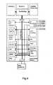
- Figure 1shows a block diagram of a data processing system 100 comprising on the left side a high-performance computing subsystem HP with both a hardware part below and a software part above. Typical in computer electronics, high-performance equipment - everything else being equal - has high power consumption.
- the right side of the diagramshows a corresponding low-performance subsystem LP having lower power consumption compared with the high-performance subsystem HP.
- Both software and hardwareare divided into layers with the common desktop 170, 175 at top, making the data processing system as a whole appear to the user substantially as a single computing device. Below the common desktop is the application layer 160, 165 followed by the operating system.
- the high-performance subsystem HPcan be set into a different state which conserves power or even be switched off completely when the low-performance subsystem executes the software.
- the low-performance subsystem LPis always active and runs the basic administration of the total system, and also 'Always-On' devices like any communication equipment (GPS, RF-modules, network interfacing components - NIC, WiFi, Bluetooth, GPRS, CDMACertainly may be connected to the LP sub-system.
- the operating systems (OS) 150,155 running on the subsystemsare adapted to their respective computing performance and tasks.
- the display means(typically a LCD-screen) is controlled by the low-performance subsystem LP while the high-performance subsystem HP is in a power saving/- hibernating/off state, and by the high-performance subsystem HP while the HP subsystem is executing the software application or user programs - also called "main operation" - requiring high-performance computing resources.
- both systemscomprise their own main processor, graphical processor and storage adapted to the specific requirements.
- At least one communication link 190interconnects the high-performance subsystem HP with the low-performance subsystem LP.
- This communication link 190can provide a connection from the low-performance subsystem LP to the high-performance HP subsystem.
- This linkuses IP/TCP or other protocols to link the two systems together.
- the physical linkis between I/O areas of respective systems. Peripheral devices can be shared using this link or by using a wider connection on the I/O Hub. This is dependent upon required system performance.
- the subsystemstypically share a common basic input/output system (BIOS) and an Advanced Configuration and Power Interface (ACPI).
- BIOSbasic input/output system
- ACPIAdvanced Configuration and Power Interface
- a 'switch' 180,185being a physical switch, a selector item as a part of the user interface on the computer display, or a result of software based evaluating a set of predetermined factors internal to the data processing system.
- the switchchanges typically the connection 125 of peripheral devices to that subsystem which is intended to execute the application program. This will allow the system to function in two distinct modes, each of which will be recognized by all peripheral devices as "Master" of the system depending on which CPU is active.
- FIGs 2 and 3show a block diagram of the x 86 architecture.
- Processor, volatile memory and graphics processing meansare connected together and to the Southbridge by the Northbridge.
- the Southbridgeacts as an I/O-hub for a number of protocols (SATA, PCIe, USB%) and provides connectivity also for the low-performance subsystem LP.
- this connectivityis as an example provided by a PCIe, forming the link to access the HP subsystem peripheral devices, and a USB channel used to transmit and receive data across the IP link 190, while figure 3 uses USB and UART for the same purposes.
- the figures 2 and 3indicate an implementation of the low-performance subsystem on the motherboard being a chip that sits next to the Southbridge and interfaces via any number of protocols while figure 6 indicates the LP-subsystem being a detachable unit (PDA and the like), equipped with UI inputs (Keyboard, touchscreen, jog wheel, "five way directional pad” or similar inputs and display.), power source, antennas for embedded RF devices, ports, small screen UI suited to its form factor and use and other features characteristic of the product category.
- PDAdetachable unit
- UI inputsKeyboard, touchscreen, jog wheel, "five way directional pad” or similar inputs and display.
- power sourceantennas for embedded RF devices
- portssmall screen UI suited to its form factor and use and other features characteristic of the product category.
- FIG. 4shows the block diagram of one possible embodiment of the present invention where the low-performance subsystem LP is implemented as a part of the x86 architecture Southbridge, this Southbridge also called the input/- output hub 120.
- An internal shared busconnects all internal I/O interface modules (PCIe, LAN, USB, AUDIO, SATA, IDE, DMA) and internal system administration modules (RESET, POWER, TEST, INTERRUPT, APIC) with the Northbridge, the BIOS and the integrated low-performance processor (ARM for instance), which in turn connects to external non-volatile memory, volatile memory, graphics, radio equipment and possibly more.
- Figure 6shows an embodiment of the invention where the low-performance system is implemented as a PCIe card - both standard format and mini-PCIe for notebooks are possible.
- the cardalso comprises keyboard, mouse and display connectors and furthermore LAN, SATA, USB, AUDIO, network and other connectors enabling it to act as a low-performance, low-power subsystem LP according to the principles of the present invention.
- keyboard, mouse and display connectorsand furthermore LAN, SATA, USB, AUDIO, network and other connectors enabling it to act as a low-performance, low-power subsystem LP according to the principles of the present invention.
- Figure 7illustrates an embodiment of the invention, where the low-performance subsystem LP - together with an additional power supply and user interface means - forms a removable stand-alone data processing system like a PDA, Smartphone or the like, which together with a substantially larger unit provides a full-featured computing environment, but removed from this full-featured computing environment provides an ultra-portable minor-performance computing unit.
- the presence of a second distinct CPUis used for multitasking and server client/protocols within the system where for example, tasks which are performed more power-efficiently on an ARM processor, can be handled by the secondary processor even when the x86 is active.
- ARMfunctions as a slave processor for the x86, handling always on task such as GPRS, GPS and other radios, an Audio could also be handled by the ARM if so chosen.
- the ARMwould function as a server for the x86 system exposing services to the HP OS.
- both subsystemshere being represented by the x86 known from the PC, and the ARM processor, typically applied in embedded applications such as mobile phones and PDA's.
- State 210is entered. Still the x86 remains off while the ARM is booting. After booting, the ARM enters state 220 (low power mode). After transition 215 ARM boot is finished.
- the low-performance subsystemis now in state 220 "Low Power Mode".
- the ARMis in control of the device.
- This mode of operationallows users to perform various computing tasks with full access to peripheries on the device (such as hard drives and embedded radio frequency devices, cameras, other).
- computing tasksmight include light office work, editing of documents, Use of calendar, email, music playback, video playback, personal entertainment programs and similar activities.
- the x86On a signal given the system enters 225 the state 230 and the high-performance x86 type processor starts its boot/resume routine.
- state 230the x86 is executing its boot sequence and gathers desktop and user environment information from database(s).
- the desktop, the user I/O and environmentthat is pointing devices, character input and shared desktop, user settings for instance
- the usermay be notified of this process via UI cue otherwise it is undisturbed by said process.
- a signaltransfers 235 the system over to state 240 indicating that the x86 has finished its boot sequence. At this point both processors and OS are running. Here error checking and data hand off for desktop and user environment may occur.
- the desktop and the user I/O and environmentthat is pointing device, character input and shared desktop
- the transition 245shows that the processes of state 240 have been completed and state 250 is entered where switching user I/O between respective subsystems occurs. This may be characterized by a momentary flicker on the display means. An image from BIOS may be displayed, an on-screen timer, or other UI niceties may be used.
- Transition 255makes the system indicating that hand off of user I/O is complete and arriving in state 260 - "Full power mode". In this mode the x86 controls both the UI and peripheries.
- Transition 265upon a signal transfers into state 270 making the x86 to start to shutdown, 'hibernate' or 'sleep', switching user I/O between respective subsystems. This again may be characterized by a momentary flicker on the screen.
- User environmentis described for ARM system. An image from BIOS may be displayed, an on-screen timer, or other UI niceties may be used.
- transition 275hand off of user I/O is complete and the system arrives at state 280 - "Low Power Mode".
- the low-performance subsystemis in control of the device.
- This mode of operationallows users to perform various computing tasks with full access to peripheries on the device (such as hard drives and embedded radios). With an ARM processor such tasks might include light office work, editing of documents, use of calendar, email, music playback, video playback, personal entertainment programs and similar activities.
- the transition 285indicates the x86 shutdown/sleep/hibernation process continues until completed.
- the systemarrives at state 220 again.
- a timeout function during this statecan transfer 289 the system into state 290, a standby state where even the ARM is in a sleep-mode, some user I/O is off, the whole system consuming even less power.
- Any wake-up event(PoC - Point of Contact, ex. keyboard input, incoming call on GPRS, calendar event) will initiate the opposite transition 291 and put the system in state 220.
- the inventionconcerns also a method according to the flow chart in figure 8 to coordinate the two subsystems in order to transparently move the software to be executed between the subsystems making these subsystems to act as a single computing device.
- the methodcomprises two procedures, the first procedure executed on the first subsystem comprising the steps: (a) gathering information about the state of the software on the first subsystem including information about allocated resources (300); then (b) storing the this state information to a storage means shared by both subsystems (310), and (c) closing down the software on the first subsystem including releasing/unmounting the resources (320).
- the second procedureexecutes on the second subsystem and includes the steps (i) fetching the stored information about the first state of the software from the shared storage means (330), (ii) starting up the software on the second subsystem comprising also allocating/mounting the resources according to the above mentioned saved state information (340), (iii) establishing a second state on the second subsystem corresponding to information about the first state (350), and (iv) saving the second state information to a storage means shared by both subsystems (360).
- a final step (d) in the first procedurecomprises putting the first subsystem into a passive, power saving state.
- parts of the state information on the storage meansare updated dynamically, when these part are observed to change on the subsystem, are updated sequentially as the operating system is in process, or are updated as system resources become available to execute background tasks.
- the present inventioncan be embodied as combinations of software and hardware modules, but will typically be implemented as a set of hardware gate logic optimized for use in a given chipset and integral with the mentioned input/output hub ("Southbridge").
Landscapes
- Engineering & Computer Science (AREA)
- Theoretical Computer Science (AREA)
- Physics & Mathematics (AREA)
- General Engineering & Computer Science (AREA)
- General Physics & Mathematics (AREA)
- Power Sources (AREA)
Description
- The present invention relates to computer hardware and software. Specifically it relates to a computer system architecture to reduce electrical power consumption.
- With ever increasing computing power - increased clock frequency, more memory, wider data paths - also power consumption of computing equipment has increased. This in turn requires increased effort in removal of dissipated heat from the electronic components but also larger power supplies or - in case of mobile equipment - better energy storage (batteries). Many innovations have been implemented to reduce power consumption, but still the typical laptop drains its battery in less than a working day.
- Besides reduction of power requirements in the field of the basic electronics (lower operational voltage for circuits f inst), some work has been done to also save power by simply powering down/switching off parts of a complex computing system when those parts are not needed for the current operation. The dichotomy is that computers often stand idle but consuming large amounts of power to maintain powerful processing capacitates, which is used only upon occasion. Many individuals computing needs could be met with little more than a smart-phones computing capacity.
- Some attempts to address this issue have been made:
- The international patent application
WO2004064119 relates to a dual processor architecture - "Dualcor" - with two different processors and two operating systems (OS). These processors in this application are integrated on a single chip and share memory and graphics systems. - The Dualcor most resembles Intel patent number
20030088800 with the exception that it uses two OS to facilitate handheld use (read functionality) and reduced power consumption. Its claims are very similar to that of the Dualcor patent application. - An application presented by Marvell World,
20050182980 integrates a PDA (Personal digital Assistant) on to a Notebook computer, allowing the user to access the personal information management (PIM), email, and media (music) on a secondary screen with a several button input while allowing the x86 system to remain off, thus saving power. The computer includes a primary processor, a primary memory, and a primary input/output (I/O) interface that communicates with the primary processor and the primary memory. A primary display communicates with the primary I/O interface. The primary processor, the primary memory, and the primary display are operated in active and inactive modes and powered down when the computer is in the inactive mode. A secondary processor dissipates less power than the primary processor. A secondary display communicates with the secondary processor. The secondary processor and the secondary display are powered up when the computer is in the inactive mode. The secondary processor and display support PDA-like functionality when the computer is in the inactive mode. - The
US patent application 20020129288 discloses a computing device having a low power secondary processor coupled to a keyboard controller for the primary applications: Media Notebooks - Instant on DVD/TV, which is designed to be installed over existing x86 systems. As such it does not have access to system components such as USB. In point 0017 of the patent it does provide for network connections, this seems to be directed toward connection to the Internet. The patent makes a full range of system peripheries available to the "secondary processor". - Another
US patent application 20030088800 presents a multi-processor mobile computer system having one low power processor integrated within a "highly integrated chipset" (Combined Northbridge and Southbridge) and a conventional main processor, thus creating a computer system having two processors of different clock frequencies and different levels of power consumption. An interface circuit can select one of the two processors to operate at a time to reduce power consumption without compromising the system performance. US 2003/0163666 A1 discloses managing software within a data processing system comprising low and high performance computing subsystems.- Still there is a need for improving the prior art, which the present invention will do in several aspects.
- The present invention relates to a data processing system comprising a high-performance computing subsystems HP involving generally high power consumption and a low-performance computing subsystems LP having low power consumption. The invention is characterized in that the data processing system acts as a single computing device by moving the execution of a main operation alternatively to the high-performance subsystems HP when high computing performance is needed or the low-performance subsystems LP when low computing performance is sufficient. In the latter case the high-performance HP subsystems can be put into a power saving state.
- The invention relates also to a method to coordinate a LP subsystem and a HP subsystem in a data processing system in order to transparently move a software between the subsystems making the subsystems to act as a single computing device. After an initial booting step (a) bringing the LP subsystem from off 200 to power-on 205 and keeping the HP subsystem powered-off 210 the method enters 215 a wait state (b), 220. On need for
high computing performance 225, said HP subsystem is booted 230, 235 entering a booted state 240. In the next step control of user interface means is transferred to the HP subsystem and the software to be executed is started 245, 250, 255, 260. In a situation of annulment of theneed 265 for high computing performance, control of the user interface means is transferred to the LP subsystem, the software is stopped and resources released 270, 275. Then the HP subsystem is transferred into a power-saving mode and the method brings the system finally back to the wait state of step (b) 280, 285, 220. - The invention relates further to a method to coordinate at least two subsystems in a data processing system in order to transparently move an active main operation between those subsystems making those subsystems to act as a single computing device. This is done by two procedures, wherein the first procedure executes on the first subsystems and comprises the steps of (a) gathering information about the state of the main operation on the first subsystems, which comprises the state of allocated resources, (b) saving this state information to a storage means shared by both subsystems and (c) closing down the main operation on the first subsystems comprising releasing resources. The second procedure executing on a second subsystems comprises the steps of (i) fetching the saved information about the first state of the main operation from the shared storage means, (ii) starting up the main operation on the second subsystems comprising allocating resources according to the saved state information, and (iii) establishing a state on the second subsystems corresponding to the information about the first statue.
- The invention is defined according to the system of claim 1 and the method of claim 20.
- Below the present invention will be described in greater detail with reference to the attached drawings, in which
Figure 1 shows the block diagram of the complete data processing system structured in hardware, software, low-performance and high-performance subsystems and shared equipment,Figure 2 shows a block diagram of the system more specifically aimed at the x86 architecture, presenting the low-performance processor connected to the I/O hub by PCI e and USB interface;Figure 3 gives a similar view asFigure 2 , but the LP-processor connects using USP and UART;Figure 4 shows the block diagram of a x86-"Southbridge" with the LP processor integrated;Figure 5 presents the state diagram for the process of moving the execution of application programs between the low- and high-performance subsystems;Figure 6 illustrates an implementation as PCIe-card (=PCI express) for the x86 architecture;Figure 7 presents a block diagram for a detachable, stand-alone, low-performance module implementation; whileFigure 8 corresponds to two procedures used in synchronizing both subsystems.- Preferred embodiments of the present invention will now be described in detail with reference to the attached drawings.
- The circumstance of unwanted high power consumption creates an opening for a computing system which is comprised of a high performance subsystem and a low performance subsystem. These two subsystems are then merged via hardware and software integration to create a single system.
- In the industry standard situation, the invention can be implemented - but is not limited to it - in the x86 architecture best known as the PC architecture using the industry standard Intel x86 processor family or compatible processors which is used throughout this document as an example, but not limitation, for a high-performance, high-powered processor. The x86 architecture comprises the so-called Northbridge organizing the access of the central processor to internal volatile memory, the graphic processing and to the so-called Southbridge. The Southbridge handles all other 10 and system management. The Northbridge and the above mentioned equipment attached to it, can be considered as the high-performance subsystem HP. Then, according to the present invention, a low-performance subsystem can be connected to or integrated into the Southbridge using a low-power, low-performance processor. This could for instance be an industry-standard ARM RISC-processor which will be used as an example, but not limitation in this document.
Figure 1 shows a block diagram of a data processing system 100 comprising on the left side a high-performance computing subsystem HP with both a hardware part below and a software part above. Typical in computer electronics, high-performance equipment - everything else being equal - has high power consumption. The right side of the diagram shows a corresponding low-performance subsystem LP having lower power consumption compared with the high-performance subsystem HP. Both software and hardware are divided into layers with thecommon desktop 170, 175 at top, making the data processing system as a whole appear to the user substantially as a single computing device. Below the common desktop is theapplication layer - In any case the low-performance subsystem LP is always active and runs the basic administration of the total system, and also 'Always-On' devices like any communication equipment (GPS, RF-modules, network interfacing components - NIC, WiFi, Bluetooth, GPRS, CDMA...) may be connected to the LP sub-system. The operating systems (OS) 150,155 running on the subsystems are adapted to their respective computing performance and tasks.
- To give the user the impression of working on a single computing device, it is important to retain a user interface and a use of peripheral devices independent, on which one of the subsystems the software is executed. To achieve this, the display means (typically a LCD-screen) is controlled by the low-performance subsystem LP while the high-performance subsystem HP is in a power saving/- hibernating/off state, and by the high-performance subsystem HP while the HP subsystem is executing the software application or user programs - also called "main operation" - requiring high-performance computing resources.
- As rather independent (sub-) systems of their own with largely different requirements for performance and power consumption, both systems comprise their own main processor, graphical processor and storage adapted to the specific requirements.
- For further supporting the cooperation of the operating system of both subsystems, at least one communication link 190 (IP link) interconnects the high-performance subsystem HP with the low-performance subsystem LP. This communication link 190 can provide a connection from the low-performance subsystem LP to the high-performance HP subsystem. This link uses IP/TCP or other protocols to link the two systems together. Although diagrammed in the software layer, the physical link is between I/O areas of respective systems. Peripheral devices can be shared using this link or by using a wider connection on the I/O Hub. This is dependent upon required system performance.
- The subsystems typically share a common basic input/output system (BIOS) and an Advanced Configuration and Power Interface (ACPI).
- The decision on which of the subsystems the execution of the application program shall be moved to, is in one preferred embodiment indicated by a 'switch' 180,185, being a physical switch, a selector item as a part of the user interface on the computer display, or a result of software based evaluating a set of predetermined factors internal to the data processing system.
- The switch changes typically the
connection 125 of peripheral devices to that subsystem which is intended to execute the application program. This will allow the system to function in two distinct modes, each of which will be recognized by all peripheral devices as "Master" of the system depending on which CPU is active. Figures 2 and 3 show a block diagram of the x 86 architecture. Processor, volatile memory and graphics processing means are connected together and to the Southbridge by the Northbridge. The Southbridge acts as an I/O-hub for a number of protocols (SATA, PCIe, USB...) and provides connectivity also for the low-performance subsystem LP. Infigure 2 this connectivity is as an example provided by a PCIe, forming the link to access the HP subsystem peripheral devices, and a USB channel used to transmit and receive data across theIP link 190, whilefigure 3 uses USB and UART for the same purposes.- The
figures 2 and 3 indicate an implementation of the low-performance subsystem on the motherboard being a chip that sits next to the Southbridge and interfaces via any number of protocols whilefigure 6 indicates the LP-subsystem being a detachable unit (PDA and the like), equipped with UI inputs (Keyboard, touchscreen, jog wheel, "five way directional pad" or similar inputs and display.), power source, antennas for embedded RF devices, ports, small screen UI suited to its form factor and use and other features characteristic of the product category. Figure 4 shows the block diagram of one possible embodiment of the present invention where the low-performance subsystem LP is implemented as a part of the x86 architecture Southbridge, this Southbridge also called the input/-output hub 120. An internal shared bus connects all internal I/O interface modules (PCIe, LAN, USB, AUDIO, SATA, IDE, DMA) and internal system administration modules (RESET, POWER, TEST, INTERRUPT, APIC) with the Northbridge, the BIOS and the integrated low-performance processor (ARM for instance), which in turn connects to external non-volatile memory, volatile memory, graphics, radio equipment and possibly more.Figure 6 shows an embodiment of the invention where the low-performance system is implemented as a PCIe card - both standard format and mini-PCIe for notebooks are possible. In addition to the components mentioned above in connection with the description of the other embodiments, here the card also comprises keyboard, mouse and display connectors and furthermore LAN, SATA, USB, AUDIO, network and other connectors enabling it to act as a low-performance, low-power subsystem LP according to the principles of the present invention. As being able already today, they could listen to network wake-up signals, but unlike today, they would in many cases not need to wake up the complete workstation, but rather do the requested job on their own.Figure 7 illustrates an embodiment of the invention, where the low-performance subsystem LP - together with an additional power supply and user interface means - forms a removable stand-alone data processing system like a PDA, Smartphone or the like, which together with a substantially larger unit provides a full-featured computing environment, but removed from this full-featured computing environment provides an ultra-portable minor-performance computing unit.- As a further embodiment of the invention, the presence of a second distinct CPU is used for multitasking and server client/protocols within the system where for example, tasks which are performed more power-efficiently on an ARM processor, can be handled by the secondary processor even when the x86 is active. In one case ARM functions as a slave processor for the x86, handling always on task such as GPRS, GPS and other radios, an Audio could also be handled by the ARM if so chosen. In another case the ARM would function as a server for the x86 system exposing services to the HP OS.
- The possible state-switching logic according to the present invention is given in
figure 5 . Minor variants may occur dependant on implementations of the present invention. - It starts - state 200 - with the combined system being powered off: both subsystems, here being represented by the x86 known from the PC, and the ARM processor, typically applied in embedded applications such as mobile phones and PDA's.
- Upon powering-on - transition 205 - from OFF-
state 200 the LPBoot process begins. State 210 is entered. Still the x86 remains off while the ARM is booting. After booting, the ARM enters state 220 (low power mode). Aftertransition 215 ARM boot is finished.- The low-performance subsystem is now in state 220 "Low Power Mode". In this state the ARM is in control of the device. This mode of operation allows users to perform various computing tasks with full access to peripheries on the device (such as hard drives and embedded radio frequency devices, cameras, other). With an ARM processor such tasks might include light office work, editing of documents, Use of calendar, email, music playback, video playback, personal entertainment programs and similar activities.
- On a signal given the system enters 225 the state 230 and the high-performance x86 type processor starts its boot/resume routine. In state 230 the x86 is executing its boot sequence and gathers desktop and user environment information from database(s). The desktop, the user I/O and environment (that is pointing devices, character input and shared desktop, user settings for instance) remain in the control of the low-performance processor. The user may be notified of this process via UI cue otherwise it is undisturbed by said process. A signal transfers 235 the system over to state 240 indicating that the x86 has finished its boot sequence. At this point both processors and OS are running. Here error checking and data hand off for desktop and user environment may occur. The desktop and the user I/O and environment (that is pointing device, character input and shared desktop) still remain under the control of the low-performance processor.
- The
transition 245 shows that the processes of state 240 have been completed andstate 250 is entered where switching user I/O between respective subsystems occurs. This may be characterized by a momentary flicker on the display means. An image from BIOS may be displayed, an on-screen timer, or other UI niceties may be used. Transition 255 makes the system indicating that hand off of user I/O is complete and arriving in state 260 - "Full power mode". In this mode the x86 controls both the UI and peripheries.Transition 265 upon a signal transfers into state 270 making the x86 to start to shutdown, 'hibernate' or 'sleep', switching user I/O between respective subsystems. This again may be characterized by a momentary flicker on the screen. User environment is described for ARM system. An image from BIOS may be displayed, an on-screen timer, or other UI niceties may be used.- After
transition 275 hand off of user I/O is complete and the system arrives at state 280 - "Low Power Mode". In this state the low-performance subsystem is in control of the device. This mode of operation allows users to perform various computing tasks with full access to peripheries on the device (such as hard drives and embedded radios). With an ARM processor such tasks might include light office work, editing of documents, use of calendar, email, music playback, video playback, personal entertainment programs and similar activities. - The
transition 285 indicates the x86 shutdown/sleep/hibernation process continues until completed. The system arrives at state 220 again. - A timeout function during this state can transfer 289 the system into state 290, a standby state where even the ARM is in a sleep-mode, some user I/O is off, the whole system consuming even less power. Any wake-up event (PoC - Point of Contact, ex. keyboard input, incoming call on GPRS, calendar event) will initiate the
opposite transition 291 and put the system in state 220. - The invention concerns also a method according to the flow chart in
figure 8 to coordinate the two subsystems in order to transparently move the software to be executed between the subsystems making these subsystems to act as a single computing device. - The method comprises two procedures, the first procedure executed on the first subsystem comprising the steps: (a) gathering information about the state of the software on the first subsystem including information about allocated resources (300); then (b) storing the this state information to a storage means shared by both subsystems (310), and (c) closing down the software on the first subsystem including releasing/unmounting the resources (320). The second procedure executes on the second subsystem and includes the steps (i) fetching the stored information about the first state of the software from the shared storage means (330), (ii) starting up the software on the second subsystem comprising also allocating/mounting the resources according to the above mentioned saved state information (340), (iii) establishing a second state on the second subsystem corresponding to information about the first state (350), and (iv) saving the second state information to a storage means shared by both subsystems (360).
- In a typical embodiment a final step (d) in the first procedure comprises putting the first subsystem into a passive, power saving state.
- According to one embodiment of the invention parts of the state information on the storage means are updated dynamically, when these part are observed to change on the subsystem, are updated sequentially as the operating system is in process, or are updated as system resources become available to execute background tasks.
- Generally speaking the present invention can be embodied as combinations of software and hardware modules, but will typically be implemented as a set of hardware gate logic optimized for use in a given chipset and integral with the mentioned input/output hub ("Southbridge").
Claims (26)
- A data processing systemcharacterized by:a high-performance computing subsystem having a first processor,a low-performance computing subsystem having a second processor independent from said first processor and said low-performance computing subsystem having lower power consumption and lower computing performance than said high-performance computing subsystem, anda controller coupled to said high-performance computing subsystem and to said low-performance computing subsystem;said low-performance computing subsystem :(i) being configured to be controlled by said controller, and(ii) being configured to:boot in an initial step from off (200) to power-on (205), while keeping said high-performance computing sub-system powered-off (210), and enter (215) a low-power waiting state (220),enter upon an inactivity timeout (289) a standby state (290);return upon a wake-up event (291) to said low-power waiting state (220); and(iii) being configured to control said data processing system to act as a single computing device by moving software execution to one of:said high-performance computing subsystem when high computing performance is needed (225) by booting said high-performance computing subsystem (230, 235) into a booted state (240), transferring control of user interface means to said high-performance computing subsystem and running said software (245, 250, 255, 260), orsaid low-performance computing subsystem when low computing performance is sufficient, by transferring control of user interface means to said low-performance computing sub-system, and stopping said software (270, 275); andif said low computing performance is sufficient, to put said high-performance computing subsystem into a power saving mode, thereby arriving at said low-power waiting state (280, 285, 220).
- Data processing system according to claim 1,
characterized in that said low-performance computing subsystem performs at least one task even when said high-performance computing subsystem is actively executing said software. - Data processing system according to claim 1,
characterized in that said data processing system retains said user interface and a use of peripheral devices independent of, on which one of said subsystems said software is executed. - Data processing system according to claim 1,
characterized in that said subsystems use operating systems being adapted to their respective computing performance. - Data processing system according to claim 1,
characterized in that said subsystems comprise their own main processing means, graphical processing means and storage means. - Data processing system according to claim 1,
characterized in that a display means is controlled by:said low-performance computing subsystem while said high-performance computing subsystem is in said power saving state, andsaid high-performance computing subsystem while said high-performance computing subsystem is executing said software. - Data processing system according to claim 1,
characterized in that at least one communication link interconnects said high-performance computing subsystem with said low-performance computing subsystem. - Data processing system according to claim 5 or 7,
characterized in that said communication link provides said connection to an input/output hub on said high-performance computing subsystem. - Data processing system according to claim 8,
characterized in that peripheral devices are shared using said communication link. - Data processing system according to claim 1,
characterized in that said subsystems share a basic input/output system. - Data processing system according to claim 1,
characterized in that a decision on which of said subsystems said execution of said software shall be moved in, is indicated by a switch being at least one of:a physical switch,a selector as a part of said user interface on said display means, anda result of evaluating a set of predetermined factors internal to said data processing system. - Data processing system according to claim 11,
characterized in that said switch is arranged to change a connection of peripheral devices to said subsystem, said subsystem being indicated to execute said software. - Data processing system according to claim 12,
characterized in that said low-performance computing subsystem is detachable from said data processing system, providing-together with necessary power supply and user interface means-a stand-alone data processing system. - Data processing system according to claim 1,
characterized in that said low-performance subsystem is used for at least one of multitasking and server/client protocols within said data processing system, executing tasks on behalf of said high-performance computing subsystem. - Data processing system according to claim 1,
characterized in that said low-performance computing subsystem acts as a slave processor for said high-performance computing subsystem. - Data processing system according to claim 1,
characterized in that said low-performance computing subsystem is arranged to handle 'always-on' tasks. - Data processing system according to claim 16,
characterized in that said 'always-on'-tasks comprise drivers for radio input/output, audio-applications, wake-up functions. - Data processing system according to claim 1,
characterized in that said low-performance computing subsystem acts as a server for said high-performance computing subsystem. - Data processing system according to claim 1,
characterized in that said data processing system is based on 'core logic' architecture, and said controller is part of said core logic. - A method to coordinate a low-performance computing subsystem and a high-performance computing subsystem in a data processing system in order to transparently move a software to be executed between said subsystems making said subsystems to act as a single computing device, the methodcharacterized in the following steps:controlling said low-performance computing subsystem to:boot in an initial step, using a second processor of said low-performance subsystem, from off (200) to power-on (205), while keeping said high-performance computing subsystem powered-off (210), said high-performance sub-system having a first processor independent of said second processor;enter (215) a low-power waiting state (220);on an inactivity timeout (289), enter a standby state (290);return on a wake-up event (291) to said low-power waiting state (220); and when there is a need for high computing performance (225), to boot said high-performance computing subsystem (230, 235) into a booted state (240);transfer control of user interface means to said high-performance computing subsystem and run said software (245, 250, 255, 260); alternatively:when there is no need (265) for high computing performance, to transfer control of said user interface means to said low-performance computing subsystem and stop said software (270, 275); andif said low computing performance is sufficient, to put said high-performance computing subsystem into a power-saving mode, thereby arriving at said low-power waiting state (280, 285, 220).
- Method according to claim 20,
characterized in alternatively to enter a state of standby (290) when an inactivity timeout occurs (289) and returning to said low-power waiting state (220) on a wake-up event (291). - Method according to claim 20,
characterized in stopping said software and saving a reentry point on one of said subsystems-a first subsystem-by running a first procedure on said first subsystem comprising the steps:gathering information about a first state of said software on said first subsystem comprising allocated resources (300),storing said first state information to a storage means shared by both subsystems (310),closing down said software on said subsystem comprising releasing memory (320), andputting said first subsystem into a passive power saving state. - Method according to claim 20,
characterized in starting said software from a defined start point on one of said subsystems not being said first subsystem-a second subsystem-by running a second procedure on said second subsystem comprising the steps:fetching said stored information about said first state of said software from said shared storage means (330),starting up said software on said second subsystem comprising allocating resources according to said saved state information (340),establishing a second state on said second subsystem corresponding to said first state information (350),saving said second state information to said storage means shared by both subsystems (360). - Method according to claim 22 or 23,
characterized in that parts of said state information on said storage means are changed dynamically, when said part of said state information is changed. - Method according to claim 22 or 23,
characterized in that parts of said state information on said storage means are updated sequentially as said operating system is in process. - Method according to claim 22 or 23,
characterized in that parts of said state information on said storage means are updated sequentially as said system resources become available to execute background tasks.
Applications Claiming Priority (2)
| Application Number | Priority Date | Filing Date | Title |
|---|---|---|---|
| US75747206P | 2006-01-10 | 2006-01-10 | |
| PCT/NO2007/000010WO2007081218A1 (en) | 2006-01-10 | 2007-01-10 | Dual mode power-saving computing system |
Publications (3)
| Publication Number | Publication Date |
|---|---|
| EP1996993A1 EP1996993A1 (en) | 2008-12-03 |
| EP1996993A4 EP1996993A4 (en) | 2013-08-07 |
| EP1996993B1true EP1996993B1 (en) | 2015-03-11 |
Family
ID=38256549
Family Applications (1)
| Application Number | Title | Priority Date | Filing Date |
|---|---|---|---|
| EP07709193.2ANot-in-forceEP1996993B1 (en) | 2006-01-10 | 2007-01-10 | Dual mode power-saving computing system |
Country Status (3)
| Country | Link |
|---|---|
| US (1) | US8065536B2 (en) |
| EP (1) | EP1996993B1 (en) |
| WO (1) | WO2007081218A1 (en) |
Families Citing this family (33)
| Publication number | Priority date | Publication date | Assignee | Title |
|---|---|---|---|---|
| US8749561B1 (en) | 2003-03-14 | 2014-06-10 | Nvidia Corporation | Method and system for coordinated data execution using a primary graphics processor and a secondary graphics processor |
| US8743019B1 (en) | 2005-05-17 | 2014-06-03 | Nvidia Corporation | System and method for abstracting computer displays across a host-client network |
| US9195428B2 (en)* | 2006-04-05 | 2015-11-24 | Nvidia Corporation | Method and system for displaying data from auxiliary display subsystem of a notebook on a main display of the notebook |
| US8775704B2 (en)* | 2006-04-05 | 2014-07-08 | Nvidia Corporation | Method and system for communication between a secondary processor and an auxiliary display subsystem of a notebook |
| US20080263324A1 (en)* | 2006-08-10 | 2008-10-23 | Sehat Sutardja | Dynamic core switching |
| US20080293449A1 (en)* | 2007-05-24 | 2008-11-27 | Stephen Barlow | Method and system for partitioning a device into domains to optimize power consumption |
| JP5084372B2 (en)* | 2007-07-03 | 2012-11-28 | キヤノン株式会社 | Data processing apparatus and data processing apparatus control method |
| CN101470509B (en)* | 2007-12-27 | 2011-04-27 | 联想(北京)有限公司 | Computer system control method, computer system and notebook computer |
| US8615647B2 (en)* | 2008-02-29 | 2013-12-24 | Intel Corporation | Migrating execution of thread between cores of different instruction set architecture in multi-core processor and transitioning each core to respective on / off power state |
| US9513695B2 (en)* | 2008-06-24 | 2016-12-06 | Virident Systems, Inc. | Methods of managing power in network computer systems |
| US8736617B2 (en) | 2008-08-04 | 2014-05-27 | Nvidia Corporation | Hybrid graphic display |
| US8799425B2 (en) | 2008-11-24 | 2014-08-05 | Nvidia Corporation | Configuring display properties of display units on remote systems |
| US20100138768A1 (en)* | 2008-12-02 | 2010-06-03 | Nvidia Corporation | Simplifying Configuration Of Multiple Display Units For Common Use |
| US9075559B2 (en) | 2009-02-27 | 2015-07-07 | Nvidia Corporation | Multiple graphics processing unit system and method |
| US20100262966A1 (en)* | 2009-04-14 | 2010-10-14 | International Business Machines Corporation | Multiprocessor computing device |
| US8650425B2 (en)* | 2009-05-06 | 2014-02-11 | Via Technologies, Inc. | Computer system for processing data in non-operational state and processing method thereof |
| US9135675B2 (en)* | 2009-06-15 | 2015-09-15 | Nvidia Corporation | Multiple graphics processing unit display synchronization system and method |
| CN101930424A (en)* | 2009-06-18 | 2010-12-29 | 辉达公司 | Hybrid Optimized PC |
| US7996596B2 (en)* | 2009-07-17 | 2011-08-09 | Dell Products, Lp | Multiple minicard interface system and method thereof |
| US8766989B2 (en) | 2009-07-29 | 2014-07-01 | Nvidia Corporation | Method and system for dynamically adding and removing display modes coordinated across multiple graphics processing units |
| US9111325B2 (en) | 2009-12-31 | 2015-08-18 | Nvidia Corporation | Shared buffer techniques for heterogeneous hybrid graphics |
| CN102213973A (en)* | 2010-04-08 | 2011-10-12 | 辉达公司 | Portable computer system |
| WO2011155047A1 (en)* | 2010-06-10 | 2011-12-15 | 富士通株式会社 | Multi-core processor system, method of power control, and power control program |
| GB2491666A (en)* | 2011-06-08 | 2012-12-12 | Inst Information Industry | Green computing heterogeneous computer system |
| US20130205144A1 (en)* | 2012-02-06 | 2013-08-08 | Jeffrey R. Eastlack | Limitation of leakage power via dynamic enablement of execution units to accommodate varying performance demands |
| US9742676B2 (en) | 2012-06-06 | 2017-08-22 | International Business Machines Corporation | Highly available servers |
| US9818379B2 (en) | 2013-08-08 | 2017-11-14 | Nvidia Corporation | Pixel data transmission over multiple pixel interfaces |
| KR102149679B1 (en)* | 2014-02-13 | 2020-08-31 | 삼성전자주식회사 | Data storage device, method thereof, and data processing system including same |
| US9591582B1 (en) | 2015-09-10 | 2017-03-07 | Qualcomm Incorporated | Smart co-processor for optimizing service discovery power consumption in wireless service platforms |
| JP6642169B2 (en)* | 2016-03-23 | 2020-02-05 | 日本電気株式会社 | Computer, computer control method, and program |
| JP6849484B2 (en)* | 2017-03-03 | 2021-03-24 | キヤノン株式会社 | Information processing device, control method of information processing device, and program |
| US11430367B2 (en)* | 2017-12-14 | 2022-08-30 | Hewlett-Packard Development Company, L.P. | Displays with phosphorescent components |
| US11112849B2 (en)* | 2018-10-26 | 2021-09-07 | Silicon Laboratories Inc. | Method and apparatus for selectable high performance or low power processor system |
Family Cites Families (21)
| Publication number | Priority date | Publication date | Assignee | Title |
|---|---|---|---|---|
| US6795929B2 (en)* | 1990-03-23 | 2004-09-21 | Matsushita Electric Industrial Co., Ltd. | Data processing apparatus |
| US6058434A (en)* | 1997-11-26 | 2000-05-02 | Acuity Imaging, Llc | Apparent network interface for and between embedded and host processors |
| US6035408A (en)* | 1998-01-06 | 2000-03-07 | Magnex Corp. | Portable computer with dual switchable processors for selectable power consumption |
| US6240521B1 (en)* | 1998-09-10 | 2001-05-29 | International Business Machines Corp. | Sleep mode transition between processors sharing an instruction set and an address space |
| US6501999B1 (en)* | 1999-12-22 | 2002-12-31 | Intel Corporation | Multi-processor mobile computer system having one processor integrated with a chipset |
| US6631474B1 (en)* | 1999-12-31 | 2003-10-07 | Intel Corporation | System to coordinate switching between first and second processors and to coordinate cache coherency between first and second processors during switching |
| JP2002215597A (en)* | 2001-01-15 | 2002-08-02 | Mitsubishi Electric Corp | Multiprocessor device |
| US20020129288A1 (en)* | 2001-03-08 | 2002-09-12 | Loh Weng Wah | Computing device having a low power secondary processor coupled to a keyboard controller |
| US20030100340A1 (en)* | 2001-03-16 | 2003-05-29 | Cupps Bryan T. | Novel personal electronics device with thermal management |
| US7184003B2 (en)* | 2001-03-16 | 2007-02-27 | Dualcor Technologies, Inc. | Personal electronics device with display switching |
| US7231531B2 (en) | 2001-03-16 | 2007-06-12 | Dualcor Technologies, Inc. | Personal electronics device with a dual core processor |
| US20030065734A1 (en)* | 2001-09-29 | 2003-04-03 | Sundaram Ramakesavan | Method and apparatus for an integrated computer and PDA |
| AU2003241016A1 (en)* | 2002-05-27 | 2003-12-12 | Sendo International Limited | Processor re-start control |
| GB0212143D0 (en)* | 2002-05-27 | 2002-07-03 | Sendo Int Ltd | Processor Monitor |
| GB0212260D0 (en)* | 2002-05-28 | 2002-07-10 | Sendo Int Ltd | System wakeup |
| US7100060B2 (en)* | 2002-06-26 | 2006-08-29 | Intel Corporation | Techniques for utilization of asymmetric secondary processing resources |
| US20050066209A1 (en)* | 2003-09-18 | 2005-03-24 | Kee Martin J. | Portable electronic device having high and low power processors operable in a low power mode |
| US20050132239A1 (en)* | 2003-12-16 | 2005-06-16 | Athas William C. | Almost-symmetric multiprocessor that supports high-performance and energy-efficient execution |
| US7421602B2 (en)* | 2004-02-13 | 2008-09-02 | Marvell World Trade Ltd. | Computer with low-power secondary processor and secondary display |
| US7152171B2 (en)* | 2004-04-28 | 2006-12-19 | Microsoft Corporation | Task-oriented processing as an auxiliary to primary computing environments |
| US20060294401A1 (en)* | 2005-06-24 | 2006-12-28 | Dell Products L.P. | Power management of multiple processors |
- 2007
- 2007-01-10EPEP07709193.2Apatent/EP1996993B1/ennot_activeNot-in-force
- 2007-01-10WOPCT/NO2007/000010patent/WO2007081218A1/enactiveApplication Filing
- 2008
- 2008-01-10USUS12/087,609patent/US8065536B2/enactiveActive
Also Published As
| Publication number | Publication date |
|---|---|
| US8065536B2 (en) | 2011-11-22 |
| EP1996993A1 (en) | 2008-12-03 |
| WO2007081218A1 (en) | 2007-07-19 |
| US20090193243A1 (en) | 2009-07-30 |
| EP1996993A4 (en) | 2013-08-07 |
Similar Documents
| Publication | Publication Date | Title |
|---|---|---|
| EP1996993B1 (en) | Dual mode power-saving computing system | |
| US7353413B2 (en) | Computer system power policy adjustment in response to an affirmative indication from a user | |
| US7149837B2 (en) | Method of operating combination personal data assistant and personal computing device | |
| KR100320979B1 (en) | Mobile client computer and power management architecture | |
| US9256271B2 (en) | Predictive power management based on user category | |
| EP1591909B1 (en) | Task-oriented processing as an auxiliary to primary computing environments | |
| US10248183B2 (en) | System and method for power management | |
| CN101359273B (en) | Mode-switching in ultra mobile devices | |
| KR101479590B1 (en) | A heterogeneous computer system for executing software | |
| US9310783B2 (en) | Dynamic clock and power gating with decentralized wake-ups | |
| US9639143B2 (en) | Interfacing dynamic hardware power managed blocks and software power managed blocks | |
| US9746910B2 (en) | Supporting runtime D3 and buffer flush and fill for a peripheral component interconnect device | |
| US20090300396A1 (en) | Information processing apparatus | |
| US20100281276A1 (en) | Computer system with power source control and power source control method | |
| US8185763B2 (en) | Method of and apparatus for informing user about setting state of wake-on-LAN function | |
| TW594466B (en) | Power management method for microprocessor | |
| CN101408792A (en) | Power management device and management method thereof | |
| US10860083B2 (en) | System, apparatus and method for collective power control of multiple intellectual property agents and a shared power rail | |
| US8065547B2 (en) | Control method and computer system for advanced configuration and power interface | |
| US20240028222A1 (en) | Sleep mode using shared memory between two processors of an information handling system | |
| CN1716162A (en) | Method and device for switching multiple operating systems in dormant state |
Legal Events
| Date | Code | Title | Description |
|---|---|---|---|
| PUAI | Public reference made under article 153(3) epc to a published international application that has entered the european phase | Free format text:ORIGINAL CODE: 0009012 | |
| 17P | Request for examination filed | Effective date:20080902 | |
| AK | Designated contracting states | Kind code of ref document:A1 Designated state(s):AT BE BG CH CY CZ DE DK EE ES FI FR GB GR HU IE IS IT LI LT LU LV MC NL PL PT RO SE SI SK TR | |
| DAX | Request for extension of the european patent (deleted) | ||
| A4 | Supplementary search report drawn up and despatched | Effective date:20130704 | |
| RIC1 | Information provided on ipc code assigned before grant | Ipc:G06F 15/16 20060101ALI20130628BHEP Ipc:G06F 1/32 20060101AFI20130628BHEP | |
| GRAP | Despatch of communication of intention to grant a patent | Free format text:ORIGINAL CODE: EPIDOSNIGR1 | |
| GRAJ | Information related to disapproval of communication of intention to grant by the applicant or resumption of examination proceedings by the epo deleted | Free format text:ORIGINAL CODE: EPIDOSDIGR1 | |
| GRAP | Despatch of communication of intention to grant a patent | Free format text:ORIGINAL CODE: EPIDOSNIGR1 | |
| INTG | Intention to grant announced | Effective date:20140728 | |
| INTC | Intention to grant announced (deleted) | ||
| INTG | Intention to grant announced | Effective date:20140811 | |
| GRAS | Grant fee paid | Free format text:ORIGINAL CODE: EPIDOSNIGR3 | |
| GRAA | (expected) grant | Free format text:ORIGINAL CODE: 0009210 | |
| AK | Designated contracting states | Kind code of ref document:B1 Designated state(s):AT BE BG CH CY CZ DE DK EE ES FI FR GB GR HU IE IS IT LI LT LU LV MC NL PL PT RO SE SI SK TR | |
| REG | Reference to a national code | Ref country code:GB Ref legal event code:FG4D | |
| REG | Reference to a national code | Ref country code:CH Ref legal event code:EP | |
| RAP2 | Party data changed (patent owner data changed or rights of a patent transferred) | Owner name:CUPP COMPUTING AS | |
| REG | Reference to a national code | Ref country code:IE Ref legal event code:FG4D | |
| REG | Reference to a national code | Ref country code:AT Ref legal event code:REF Ref document number:715661 Country of ref document:AT Kind code of ref document:T Effective date:20150415 | |
| REG | Reference to a national code | Ref country code:DE Ref legal event code:R096 Ref document number:602007040564 Country of ref document:DE Effective date:20150423 | |
| REG | Reference to a national code | Ref country code:NL Ref legal event code:VDEP Effective date:20150311 | |
| REG | Reference to a national code | Ref country code:NL Ref legal event code:VDEP Effective date:20150311 | |
| PG25 | Lapsed in a contracting state [announced via postgrant information from national office to epo] | Ref country code:FI Free format text:LAPSE BECAUSE OF FAILURE TO SUBMIT A TRANSLATION OF THE DESCRIPTION OR TO PAY THE FEE WITHIN THE PRESCRIBED TIME-LIMIT Effective date:20150311 Ref country code:ES Free format text:LAPSE BECAUSE OF FAILURE TO SUBMIT A TRANSLATION OF THE DESCRIPTION OR TO PAY THE FEE WITHIN THE PRESCRIBED TIME-LIMIT Effective date:20150311 Ref country code:SE Free format text:LAPSE BECAUSE OF FAILURE TO SUBMIT A TRANSLATION OF THE DESCRIPTION OR TO PAY THE FEE WITHIN THE PRESCRIBED TIME-LIMIT Effective date:20150311 Ref country code:LT Free format text:LAPSE BECAUSE OF FAILURE TO SUBMIT A TRANSLATION OF THE DESCRIPTION OR TO PAY THE FEE WITHIN THE PRESCRIBED TIME-LIMIT Effective date:20150311 | |
| REG | Reference to a national code | Ref country code:AT Ref legal event code:MK05 Ref document number:715661 Country of ref document:AT Kind code of ref document:T Effective date:20150311 | |
| REG | Reference to a national code | Ref country code:LT Ref legal event code:MG4D | |
| PG25 | Lapsed in a contracting state [announced via postgrant information from national office to epo] | Ref country code:GR Free format text:LAPSE BECAUSE OF FAILURE TO SUBMIT A TRANSLATION OF THE DESCRIPTION OR TO PAY THE FEE WITHIN THE PRESCRIBED TIME-LIMIT Effective date:20150612 Ref country code:LV Free format text:LAPSE BECAUSE OF FAILURE TO SUBMIT A TRANSLATION OF THE DESCRIPTION OR TO PAY THE FEE WITHIN THE PRESCRIBED TIME-LIMIT Effective date:20150311 | |
| PG25 | Lapsed in a contracting state [announced via postgrant information from national office to epo] | Ref country code:NL Free format text:LAPSE BECAUSE OF FAILURE TO SUBMIT A TRANSLATION OF THE DESCRIPTION OR TO PAY THE FEE WITHIN THE PRESCRIBED TIME-LIMIT Effective date:20150311 | |
| PG25 | Lapsed in a contracting state [announced via postgrant information from national office to epo] | Ref country code:SK Free format text:LAPSE BECAUSE OF FAILURE TO SUBMIT A TRANSLATION OF THE DESCRIPTION OR TO PAY THE FEE WITHIN THE PRESCRIBED TIME-LIMIT Effective date:20150311 Ref country code:CZ Free format text:LAPSE BECAUSE OF FAILURE TO SUBMIT A TRANSLATION OF THE DESCRIPTION OR TO PAY THE FEE WITHIN THE PRESCRIBED TIME-LIMIT Effective date:20150311 Ref country code:RO Free format text:LAPSE BECAUSE OF FAILURE TO SUBMIT A TRANSLATION OF THE DESCRIPTION OR TO PAY THE FEE WITHIN THE PRESCRIBED TIME-LIMIT Effective date:20150311 Ref country code:PT Free format text:LAPSE BECAUSE OF FAILURE TO SUBMIT A TRANSLATION OF THE DESCRIPTION OR TO PAY THE FEE WITHIN THE PRESCRIBED TIME-LIMIT Effective date:20150713 Ref country code:EE Free format text:LAPSE BECAUSE OF FAILURE TO SUBMIT A TRANSLATION OF THE DESCRIPTION OR TO PAY THE FEE WITHIN THE PRESCRIBED TIME-LIMIT Effective date:20150311 | |
| PG25 | Lapsed in a contracting state [announced via postgrant information from national office to epo] | Ref country code:IS Free format text:LAPSE BECAUSE OF FAILURE TO SUBMIT A TRANSLATION OF THE DESCRIPTION OR TO PAY THE FEE WITHIN THE PRESCRIBED TIME-LIMIT Effective date:20150711 Ref country code:PL Free format text:LAPSE BECAUSE OF FAILURE TO SUBMIT A TRANSLATION OF THE DESCRIPTION OR TO PAY THE FEE WITHIN THE PRESCRIBED TIME-LIMIT Effective date:20150311 Ref country code:AT Free format text:LAPSE BECAUSE OF FAILURE TO SUBMIT A TRANSLATION OF THE DESCRIPTION OR TO PAY THE FEE WITHIN THE PRESCRIBED TIME-LIMIT Effective date:20150311 | |
| REG | Reference to a national code | Ref country code:DE Ref legal event code:R097 Ref document number:602007040564 Country of ref document:DE | |
| PG25 | Lapsed in a contracting state [announced via postgrant information from national office to epo] | Ref country code:IT Free format text:LAPSE BECAUSE OF FAILURE TO SUBMIT A TRANSLATION OF THE DESCRIPTION OR TO PAY THE FEE WITHIN THE PRESCRIBED TIME-LIMIT Effective date:20150311 | |
| PLBE | No opposition filed within time limit | Free format text:ORIGINAL CODE: 0009261 | |
| STAA | Information on the status of an ep patent application or granted ep patent | Free format text:STATUS: NO OPPOSITION FILED WITHIN TIME LIMIT | |
| PG25 | Lapsed in a contracting state [announced via postgrant information from national office to epo] | Ref country code:DK Free format text:LAPSE BECAUSE OF FAILURE TO SUBMIT A TRANSLATION OF THE DESCRIPTION OR TO PAY THE FEE WITHIN THE PRESCRIBED TIME-LIMIT Effective date:20150311 | |
| 26N | No opposition filed | Effective date:20151214 | |
| PG25 | Lapsed in a contracting state [announced via postgrant information from national office to epo] | Ref country code:SI Free format text:LAPSE BECAUSE OF FAILURE TO SUBMIT A TRANSLATION OF THE DESCRIPTION OR TO PAY THE FEE WITHIN THE PRESCRIBED TIME-LIMIT Effective date:20150311 | |
| PG25 | Lapsed in a contracting state [announced via postgrant information from national office to epo] | Ref country code:BE Free format text:LAPSE BECAUSE OF NON-PAYMENT OF DUE FEES Effective date:20160131 | |
| REG | Reference to a national code | Ref country code:DE Ref legal event code:R119 Ref document number:602007040564 Country of ref document:DE | |
| PG25 | Lapsed in a contracting state [announced via postgrant information from national office to epo] | Ref country code:LU Free format text:LAPSE BECAUSE OF FAILURE TO SUBMIT A TRANSLATION OF THE DESCRIPTION OR TO PAY THE FEE WITHIN THE PRESCRIBED TIME-LIMIT Effective date:20160110 Ref country code:BE Free format text:LAPSE BECAUSE OF FAILURE TO SUBMIT A TRANSLATION OF THE DESCRIPTION OR TO PAY THE FEE WITHIN THE PRESCRIBED TIME-LIMIT Effective date:20150311 | |
| REG | Reference to a national code | Ref country code:CH Ref legal event code:PL | |
| GBPC | Gb: european patent ceased through non-payment of renewal fee | Effective date:20160110 | |
| PG25 | Lapsed in a contracting state [announced via postgrant information from national office to epo] | Ref country code:MC Free format text:LAPSE BECAUSE OF FAILURE TO SUBMIT A TRANSLATION OF THE DESCRIPTION OR TO PAY THE FEE WITHIN THE PRESCRIBED TIME-LIMIT Effective date:20150311 | |
| REG | Reference to a national code | Ref country code:FR Ref legal event code:ST Effective date:20160930 | |
| PG25 | Lapsed in a contracting state [announced via postgrant information from national office to epo] | Ref country code:DE Free format text:LAPSE BECAUSE OF NON-PAYMENT OF DUE FEES Effective date:20160802 Ref country code:CH Free format text:LAPSE BECAUSE OF NON-PAYMENT OF DUE FEES Effective date:20160131 Ref country code:GB Free format text:LAPSE BECAUSE OF NON-PAYMENT OF DUE FEES Effective date:20160110 Ref country code:LI Free format text:LAPSE BECAUSE OF NON-PAYMENT OF DUE FEES Effective date:20160131 | |
| REG | Reference to a national code | Ref country code:IE Ref legal event code:MM4A | |
| PG25 | Lapsed in a contracting state [announced via postgrant information from national office to epo] | Ref country code:FR Free format text:LAPSE BECAUSE OF NON-PAYMENT OF DUE FEES Effective date:20160201 | |
| PG25 | Lapsed in a contracting state [announced via postgrant information from national office to epo] | Ref country code:IE Free format text:LAPSE BECAUSE OF NON-PAYMENT OF DUE FEES Effective date:20160110 | |
| PG25 | Lapsed in a contracting state [announced via postgrant information from national office to epo] | Ref country code:HU Free format text:LAPSE BECAUSE OF FAILURE TO SUBMIT A TRANSLATION OF THE DESCRIPTION OR TO PAY THE FEE WITHIN THE PRESCRIBED TIME-LIMIT; INVALID AB INITIO Effective date:20070110 Ref country code:CY Free format text:LAPSE BECAUSE OF FAILURE TO SUBMIT A TRANSLATION OF THE DESCRIPTION OR TO PAY THE FEE WITHIN THE PRESCRIBED TIME-LIMIT Effective date:20150311 | |
| PG25 | Lapsed in a contracting state [announced via postgrant information from national office to epo] | Ref country code:TR Free format text:LAPSE BECAUSE OF FAILURE TO SUBMIT A TRANSLATION OF THE DESCRIPTION OR TO PAY THE FEE WITHIN THE PRESCRIBED TIME-LIMIT Effective date:20150311 | |
| PG25 | Lapsed in a contracting state [announced via postgrant information from national office to epo] | Ref country code:BG Free format text:LAPSE BECAUSE OF FAILURE TO SUBMIT A TRANSLATION OF THE DESCRIPTION OR TO PAY THE FEE WITHIN THE PRESCRIBED TIME-LIMIT Effective date:20150311 |