EP1984954B1 - Field effect transistor using oxide film for channel and method of manufacturing the same - Google Patents
Field effect transistor using oxide film for channel and method of manufacturing the sameDownload PDFInfo
- Publication number
- EP1984954B1 EP1984954B1EP07738746AEP07738746AEP1984954B1EP 1984954 B1EP1984954 B1EP 1984954B1EP 07738746 AEP07738746 AEP 07738746AEP 07738746 AEP07738746 AEP 07738746AEP 1984954 B1EP1984954 B1EP 1984954B1
- Authority
- EP
- European Patent Office
- Prior art keywords
- drain
- source
- hydrogen
- electrode
- field effect
- Prior art date
- Legal status (The legal status is an assumption and is not a legal conclusion. Google has not performed a legal analysis and makes no representation as to the accuracy of the status listed.)
- Not-in-force
Links
- 230000005669field effectEffects0.000titleclaimsabstractdescription78
- 238000004519manufacturing processMethods0.000titleclaimsdescription17
- 229910052739hydrogenInorganic materials0.000claimsabstractdescription96
- 239000001257hydrogenSubstances0.000claimsabstractdescription96
- UFHFLCQGNIYNRP-UHFFFAOYSA-NHydrogenChemical compound[H][H]UFHFLCQGNIYNRP-UHFFFAOYSA-N0.000claimsabstractdescription87
- 229910052805deuteriumInorganic materials0.000claimsabstractdescription29
- YZCKVEUIGOORGS-OUBTZVSYSA-NDeuteriumChemical compound[2H]YZCKVEUIGOORGS-OUBTZVSYSA-N0.000claimsabstractdescription27
- 239000004065semiconductorSubstances0.000claimsabstractdescription14
- 238000000034methodMethods0.000claimsdescription60
- 239000000758substrateSubstances0.000claimsdescription45
- 108091006149Electron carriersProteins0.000claimsdescription7
- 229910052738indiumInorganic materials0.000claimsdescription3
- 229910052725zincInorganic materials0.000claimsdescription3
- 239000012212insulatorSubstances0.000claimsdescription2
- 239000010408filmSubstances0.000description116
- 239000010410layerSubstances0.000description75
- 239000010409thin filmSubstances0.000description46
- XLOMVQKBTHCTTD-UHFFFAOYSA-NZinc monoxideChemical compound[Zn]=OXLOMVQKBTHCTTD-UHFFFAOYSA-N0.000description22
- 239000000463materialSubstances0.000description21
- 230000015572biosynthetic processEffects0.000description19
- QVGXLLKOCUKJST-UHFFFAOYSA-Natomic oxygenChemical compound[O]QVGXLLKOCUKJST-UHFFFAOYSA-N0.000description15
- 239000001301oxygenSubstances0.000description15
- 229910052760oxygenInorganic materials0.000description15
- 239000000203mixtureSubstances0.000description14
- 229910007541Zn OInorganic materials0.000description13
- 239000007789gasSubstances0.000description13
- 238000005468ion implantationMethods0.000description13
- 229920003023plasticPolymers0.000description13
- 238000012545processingMethods0.000description13
- 239000004973liquid crystal related substanceSubstances0.000description12
- 239000004033plasticSubstances0.000description12
- 239000011787zinc oxideSubstances0.000description11
- 238000000059patterningMethods0.000description10
- 230000000052comparative effectEffects0.000description9
- GPRLSGONYQIRFK-UHFFFAOYSA-NhydronChemical compound[H+]GPRLSGONYQIRFK-UHFFFAOYSA-N0.000description9
- 150000002500ionsChemical class0.000description9
- 230000008569processEffects0.000description9
- 230000008859changeEffects0.000description8
- -1hydrogen ionsChemical class0.000description8
- 239000011701zincSubstances0.000description7
- XKRFYHLGVUSROY-UHFFFAOYSA-NArgonChemical compound[Ar]XKRFYHLGVUSROY-UHFFFAOYSA-N0.000description6
- 239000003990capacitorSubstances0.000description6
- 239000011521glassSubstances0.000description6
- PJXISJQVUVHSOJ-UHFFFAOYSA-Nindium(III) oxideInorganic materials[O-2].[O-2].[O-2].[In+3].[In+3]PJXISJQVUVHSOJ-UHFFFAOYSA-N0.000description6
- 230000003071parasitic effectEffects0.000description6
- 238000011156evaluationMethods0.000description5
- 239000010931goldSubstances0.000description5
- 150000002431hydrogenChemical class0.000description5
- 239000002245particleSubstances0.000description5
- 238000000206photolithographyMethods0.000description5
- 229920006255plastic filmPolymers0.000description5
- 239000002985plastic filmSubstances0.000description5
- 238000004544sputter depositionMethods0.000description5
- 238000004458analytical methodMethods0.000description4
- 150000001875compoundsChemical class0.000description4
- 210000002858crystal cellAnatomy0.000description4
- 238000005259measurementMethods0.000description4
- 229910052751metalInorganic materials0.000description4
- 239000002184metalSubstances0.000description4
- 238000001020plasma etchingMethods0.000description4
- XOLBLPGZBRYERU-UHFFFAOYSA-Ntin dioxideChemical compoundO=[Sn]=OXOLBLPGZBRYERU-UHFFFAOYSA-N0.000description4
- 238000012546transferMethods0.000description4
- 229920002799BoPETPolymers0.000description3
- 238000002441X-ray diffractionMethods0.000description3
- 229910021417amorphous siliconInorganic materials0.000description3
- 229910052786argonInorganic materials0.000description3
- 239000002775capsuleSubstances0.000description3
- 238000000151depositionMethods0.000description3
- 238000001514detection methodMethods0.000description3
- 238000011161developmentMethods0.000description3
- 230000018109developmental processEffects0.000description3
- 238000010586diagramMethods0.000description3
- 229910052737goldInorganic materials0.000description3
- 150000002739metalsChemical class0.000description3
- SLIUAWYAILUBJU-UHFFFAOYSA-NpentaceneChemical compoundC1=CC=CC2=CC3=CC4=CC5=CC=CC=C5C=C4C=C3C=C21SLIUAWYAILUBJU-UHFFFAOYSA-N0.000description3
- 229920001721polyimidePolymers0.000description3
- 238000001004secondary ion mass spectrometryMethods0.000description3
- 238000004611spectroscopical analysisMethods0.000description3
- 238000004876x-ray fluorescenceMethods0.000description3
- RUDFQVOCFDJEEF-UHFFFAOYSA-Nyttrium(III) oxideInorganic materials[O-2].[O-2].[O-2].[Y+3].[Y+3]RUDFQVOCFDJEEF-UHFFFAOYSA-N0.000description3
- MYMOFIZGZYHOMD-UHFFFAOYSA-NDioxygenChemical compoundO=OMYMOFIZGZYHOMD-UHFFFAOYSA-N0.000description2
- 125000003118aryl groupChemical group0.000description2
- 230000008901benefitEffects0.000description2
- 210000004027cellAnatomy0.000description2
- 239000011248coating agentSubstances0.000description2
- 238000000576coating methodMethods0.000description2
- 238000002425crystallisationMethods0.000description2
- 230000008025crystallizationEffects0.000description2
- 229910001882dioxygenInorganic materials0.000description2
- 230000000694effectsEffects0.000description2
- 238000000313electron-beam-induced depositionMethods0.000description2
- 238000001962electrophoresisMethods0.000description2
- 239000012530fluidSubstances0.000description2
- 229910052733galliumInorganic materials0.000description2
- PCHJSUWPFVWCPO-UHFFFAOYSA-NgoldChemical compound[Au]PCHJSUWPFVWCPO-UHFFFAOYSA-N0.000description2
- CJNBYAVZURUTKZ-UHFFFAOYSA-Nhafnium(IV) oxideInorganic materialsO=[Hf]=OCJNBYAVZURUTKZ-UHFFFAOYSA-N0.000description2
- 239000002075main ingredientSubstances0.000description2
- 239000011159matrix materialSubstances0.000description2
- 238000005268plasma chemical vapour depositionMethods0.000description2
- 229910021420polycrystalline siliconInorganic materials0.000description2
- 229920000139polyethylene terephthalatePolymers0.000description2
- 239000005020polyethylene terephthalateSubstances0.000description2
- 230000000630rising effectEffects0.000description2
- 229910052710siliconInorganic materials0.000description2
- 239000011343solid materialSubstances0.000description2
- 238000000391spectroscopic ellipsometryMethods0.000description2
- 238000002834transmittanceMethods0.000description2
- 206010007269CarcinogenicityDiseases0.000description1
- 229910001218Gallium arsenideInorganic materials0.000description1
- 239000004988Nematic liquid crystalSubstances0.000description1
- XUIMIQQOPSSXEZ-UHFFFAOYSA-NSiliconChemical compound[Si]XUIMIQQOPSSXEZ-UHFFFAOYSA-N0.000description1
- 238000000862absorption spectrumMethods0.000description1
- 229910052782aluminiumInorganic materials0.000description1
- PNEYBMLMFCGWSK-UHFFFAOYSA-Naluminium oxideInorganic materials[O-2].[O-2].[O-2].[Al+3].[Al+3]PNEYBMLMFCGWSK-UHFFFAOYSA-N0.000description1
- 238000000137annealingMethods0.000description1
- 238000005452bendingMethods0.000description1
- 230000007670carcinogenicityEffects0.000description1
- 231100000260carcinogenicityToxicity0.000description1
- 239000000969carrierSubstances0.000description1
- 239000000919ceramicSubstances0.000description1
- 229910052593corundumInorganic materials0.000description1
- 239000013078crystalSubstances0.000description1
- 238000009792diffusion processMethods0.000description1
- 239000002019doping agentSubstances0.000description1
- 238000005401electroluminescenceMethods0.000description1
- 238000005516engineering processMethods0.000description1
- 238000005530etchingMethods0.000description1
- 238000001704evaporationMethods0.000description1
- 238000013213extrapolationMethods0.000description1
- 229910021476group 6 elementInorganic materials0.000description1
- 238000002513implantationMethods0.000description1
- 230000003993interactionEffects0.000description1
- 239000011229interlayerSubstances0.000description1
- 230000031700light absorptionEffects0.000description1
- 239000007788liquidSubstances0.000description1
- 229910052749magnesiumInorganic materials0.000description1
- 239000011777magnesiumSubstances0.000description1
- PNHVEGMHOXTHMW-UHFFFAOYSA-Nmagnesium;zinc;oxygen(2-)Chemical compound[O-2].[O-2].[Mg+2].[Zn+2]PNHVEGMHOXTHMW-UHFFFAOYSA-N0.000description1
- 229910052759nickelInorganic materials0.000description1
- 229910052697platinumInorganic materials0.000description1
- 229920000642polymerPolymers0.000description1
- 229920006254polymer filmPolymers0.000description1
- 230000009467reductionEffects0.000description1
- 238000012827research and developmentMethods0.000description1
- 239000011347resinSubstances0.000description1
- 229920005989resinPolymers0.000description1
- 230000004044responseEffects0.000description1
- 229920006395saturated elastomerPolymers0.000description1
- 239000010703siliconSubstances0.000description1
- 230000001988toxicityEffects0.000description1
- 231100000419toxicityToxicity0.000description1
- 239000012780transparent materialSubstances0.000description1
- 229910001845yogo sapphireInorganic materials0.000description1
Images


Classifications
- H—ELECTRICITY
- H10—SEMICONDUCTOR DEVICES; ELECTRIC SOLID-STATE DEVICES NOT OTHERWISE PROVIDED FOR
- H10D—INORGANIC ELECTRIC SEMICONDUCTOR DEVICES
- H10D30/00—Field-effect transistors [FET]
- H10D30/60—Insulated-gate field-effect transistors [IGFET]
- H10D30/67—Thin-film transistors [TFT]
- H10D30/674—Thin-film transistors [TFT] characterised by the active materials
- H10D30/6755—Oxide semiconductors, e.g. zinc oxide, copper aluminium oxide or cadmium stannate
- H10D30/6756—Amorphous oxide semiconductors
- H—ELECTRICITY
- H10—SEMICONDUCTOR DEVICES; ELECTRIC SOLID-STATE DEVICES NOT OTHERWISE PROVIDED FOR
- H10D—INORGANIC ELECTRIC SEMICONDUCTOR DEVICES
- H10D30/00—Field-effect transistors [FET]
- H10D30/01—Manufacture or treatment
- H10D30/021—Manufacture or treatment of FETs having insulated gates [IGFET]
- H10D30/031—Manufacture or treatment of FETs having insulated gates [IGFET] of thin-film transistors [TFT]
- H—ELECTRICITY
- H10—SEMICONDUCTOR DEVICES; ELECTRIC SOLID-STATE DEVICES NOT OTHERWISE PROVIDED FOR
- H10D—INORGANIC ELECTRIC SEMICONDUCTOR DEVICES
- H10D30/00—Field-effect transistors [FET]
- H10D30/60—Insulated-gate field-effect transistors [IGFET]
- H10D30/67—Thin-film transistors [TFT]
- H10D30/6704—Thin-film transistors [TFT] having supplementary regions or layers in the thin films or in the insulated bulk substrates for controlling properties of the device
- H10D30/6713—Thin-film transistors [TFT] having supplementary regions or layers in the thin films or in the insulated bulk substrates for controlling properties of the device characterised by the properties of the source or drain regions, e.g. compositions or sectional shapes
- H10D30/6715—Thin-film transistors [TFT] having supplementary regions or layers in the thin films or in the insulated bulk substrates for controlling properties of the device characterised by the properties of the source or drain regions, e.g. compositions or sectional shapes characterised by the doping profiles, e.g. having lightly-doped source or drain extensions
- H—ELECTRICITY
- H10—SEMICONDUCTOR DEVICES; ELECTRIC SOLID-STATE DEVICES NOT OTHERWISE PROVIDED FOR
- H10D—INORGANIC ELECTRIC SEMICONDUCTOR DEVICES
- H10D30/00—Field-effect transistors [FET]
- H10D30/60—Insulated-gate field-effect transistors [IGFET]
- H10D30/67—Thin-film transistors [TFT]
- H10D30/6757—Thin-film transistors [TFT] characterised by the structure of the channel, e.g. transverse or longitudinal shape or doping profile
- H—ELECTRICITY
- H10—SEMICONDUCTOR DEVICES; ELECTRIC SOLID-STATE DEVICES NOT OTHERWISE PROVIDED FOR
- H10D—INORGANIC ELECTRIC SEMICONDUCTOR DEVICES
- H10D62/00—Semiconductor bodies, or regions thereof, of devices having potential barriers
- H10D62/10—Shapes, relative sizes or dispositions of the regions of the semiconductor bodies; Shapes of the semiconductor bodies
- H—ELECTRICITY
- H10—SEMICONDUCTOR DEVICES; ELECTRIC SOLID-STATE DEVICES NOT OTHERWISE PROVIDED FOR
- H10D—INORGANIC ELECTRIC SEMICONDUCTOR DEVICES
- H10D99/00—Subject matter not provided for in other groups of this subclass
Definitions
- the present inventionrelates to a field effect transistor including an oxide film as a semiconductor layer, a method of manufacturing the same, and a display device.
- the present inventionrelates to a field effect transistor having transistor characteristics which can be applied to a display device or the like, a method of manufacturing the same, and a display device.
- a field effect transistoris a three-terminal device having a gate electrode, a source electrode, and a drain electrode. Further, the field effect transistor is an electronic active device in which a current flowing through a channel layer (a current between a source electrode and a drain electrode) is controlled by voltage applied to a gate electrode.
- a current flowing through a channel layera current between a source electrode and a drain electrode
- a thin film FETthin film transistor, TFT.
- the devicecan be formed on an several substrates formed of ceramic, glass, plastic, or the like.
- the above-mentioned TFThas an advantage of being easily formed on a substrate having a relatively large area because the TFT uses thin film technology, and is widely used as a driving device in a flat panel display device such as a liquid crystal display device. More specifically, in an active liquid crystal display (ALCD), TFTs formed on a glass substrate are used to turn on and off individual image pixels. Also, in a prospective high performance organic LED display (OLED), it is thought to be effective to current-drive the pixels by TFTs. Further, a higher performance liquid crystal display device is realized in which a TFT circuit having a function of driving and controlling the whole image is formed on a substrate in the vicinity of an image display region.
- ACDactive liquid crystal display
- OLEDorganic LED display
- a TFT which is currently most widely usedis a metal-insulator-semiconductor field effect transistor (MIS-FET) device using a polycrytalline silicon film or an amorphous silicon film as a channel layer material.
- MI-FETmetal-insulator-semiconductor field effect transistor
- An amorphous silicon TFTis practically used for pixel driving and a high-performance polycrystalline silicon TFT is practically used for drive control of the entire image.
- pentacenehas been under research and development for the organic semiconductor film.
- the organic semiconductorhas an aromatic ring.
- Large carrier mobilityis obtained in the stack direction of the aromatic ring at the time of crystallization.
- the carrier mobilityis approximately 0.5 cm 2 (Vs) -1 , which is equal to that of an amorphous SI-MOSFET.
- the organic semiconductor such as the pentacenehas low thermal stability (it is unstable when temperature exceeds 150°C) and toxicity (carcinogenicity). Therefore, a practical device has not been realized.
- a TFT using, as the channel layer thereof, a transparent conductive oxide polycrystalline thin film containing ZnO as a main ingredienthas been under active development.
- the thin filmcan be formed at a relatively low temperature, and therefore it is possible to form the film on a substrate such as a plastic plate or a plastic film.
- a stable amorphous phasecannot be formed at a room temperature and a polycrystalline phase is formed. Therefore, it is difficult to increase an electron mobility thereof because of scattering of polycrystalline grain boundaries.
- it is difficult to achieve reproductivity in the characteristics of a TFT devicebecause a' polycrystalline grain shape and an interconnection thereof are significantly changed depending on film formation methods.
- a thin film transistor using an amorphous In-Ga-Zn-O-based oxidehas been reported by K. Nomura, et al., Nature, 432, 488 (2004 ).
- the thin film transistorcan be formed on a plastic plate or a glass substrate at a room temperature.
- the deviceshows a normally-off characteristics with field effect mobility of approximately 6 to 9.
- WO 2004/114391 A and US 2006/0244107 Adisclose a thin-film transistor where the active layer is formed of zinc oxide or magnesium zinc oxide.
- the inventors of the present inventionhave studied a thin film transistor using an oxide including an amorphous In-Ga-Zn-O oxide. As a result, there is the case where a variation in transistor characteristic (Id-Vg characteristic) of a TFT occurs, although an extent of the variation is depended on the channel materials or the manufacturing conditions etc.
- the variation in characteristiccauses a variation in operation of an organic LED or a liquid.crystal element which is to be driven, therevy finally reducing the image quality of the display.
- an object of the present inventionis to reduce the above-mentioned variation in characteristic.
- Examples of a factor of the variationinclude:
- a first object of the present inventionis to device a connection between the channel of a transistor and each of the source and drain electrodes thereof, thereby reducing the variation in characteristic.
- a second object of the present inventionis to provide a structure capable of forming the positional relationship among the gate, the source, and the drain with high precision and a manufacturing method thereof, thereby reducing the variation in characteristic.
- the present inventionprovides the field effect transistor claimed in claim 1, the display device claimed in claim 10, and the method of manufacturing a field effect transistor claimed in claim 12.
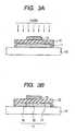
- FIGS. 1A and 1Bare cross sectional views illustrating structural examples of a field effect transistor according to an embodiment of the present invention.
- FIG. 1Aillustrates an example of a top-gate structure
- FIG. 1Billustrates an example of a bottom-gate structure.
- FIGS. 1A and 1Bprovided are on a substrate 10, a channel layer (oxide thin film) 11, a gate insulating layer 12, a source electrode 13, a drain electrode 14, a gate electrode 15, a source part 16, a drain part 17, and a channel part 18.
- the channel layer 11includes the source part 16, the drain part 17, and the channel part 18.
- the gate insulating layer 12 and the gate electrode 15are formed on the channel layer 11 in mentioned order, thereby obtaining the top-gate structure.
- the gate insulating layer 12 and the channel layer 11are formed on the gate electrode 15 in mentioned order, thereby obtaining the bottom-gate structure.
- the source part and the drain partalso serve as the source electrode and the drain electrode, respectively.
- the channel part of the transistor and the source electrode (drain electrode)are connected with each other through the source part (drain part).
- the oxide thin film which is the channel layer 11includes the channel part 18, the source part 16, and the drain part 17.
- the source part 16 and the drain part 17are added with hydrogen or deuterium to reduce a resistivity thereof.
- the concentration of hydrogen or deuterium of each of the source part 16 and the drain part 17is set to a value larger than the concentration of hydrogen or deuterium of the channel part 18.
- the electric conductivity of the source part (drain part)can be increased by the addition of hydrogen or deuterium thereto.
- the concentration of hydrogen or deuterium of the source part (drain part)is increased to a value larger than the concentration of hydrogen or deuterium of the channel part 18, the electric conductivity of the source part (drain part) can be set to a value larger than the electric conductivity of the channel part.
- the channel part and the source (drain) electrodecan be electrically connected with each other with high reliability, whereby a thin film transistor having small variation can be realized.
- the source part and the drain partare formed in the oxide film. Therefore, stable electrical connection can be made in comparison with the case of a conventional structure in which the source electrode and the drain electrode are directly formed on the oxide film.
- a top-gate structure, a bottom-gate structure, a staggered structure, or a coplanar structurecan be arbitrarily used as the structure of the field effect transistor.
- the coplanar structure illustrated in FIG. 1Amay be used.
- the source and drain electrodesare directly connected with an interface between the gate insulating layer and the channel layer, and high-reliability electrical connection can be attained.
- the transistor according to this embodimentmay have a structure in which the gate electrode and the source (drain) part are formed in self-alignment. That is, as described later, hydrogen is added to the oxide film by using a pattern of the gate electrode as a mask, whereby the source part and the drain part in self-alignment with respect to the pattern of the gate electrode are formed in the oxide film.
- a transistorWhen the self-alignment method is used, a transistor can be realized in which the overlap between the source (drain) part and the gate electrode is small and uniform. As a result, a parasitic capacitance of the transistor which is caused in an overlap portion' between the gate electrode and the drain part can be reduced and made uniform. Because of the small parasitic capacitance, high-speed operation can be realized. Because of the uniform parasitic capacitance, a transistor excellent in uniform characteristics is can be realized.
- the source part 16 and the drain part 17are added with hydrogen or deuterium to reduce resistivity thereof.
- the inventors of the present inventionfound that, when hydrogen (or deuterium) is added to an amorphous In-Ga-Zn-O thin film, the electric conductivity of the oxide thin film becomes larger.
- the channel part 18contains hydrogen or deuterium, the concentration of hydrogen or deuterium of each of the source part and the drain part is increased to a value larger than the concentration of hydrogen or deuterium of the channel part, so electrical connecting can be improved.
- FIG. 2is a characteristic graph illustrating an example of a relationship between a hydrogen ion implantation amount and resistivity.
- FIG. 2illustrates a change in electric conductivity to the hydrogen ion implantation amount in the case where ions are implanted into an InGaZnO 4 thin film having a film thickness of approximately 500 nm.
- the abscissa (x-axis)is a logarithmic representation of the hydrogen ion implantation amount per unit area and the ordinate (y-axis) is a logarithmic representation of the resistivity. Therefore, hydrogen can be added to the amorphous oxide film to control the electric conductivity.
- the electric conductivity thereofcan be increased.
- the concentration of hydrogen of each of the source part and the drain partis increased to a value larger than the concentration of hydrogen of the channel part. Therefore, the electric conductivity of each of the source part and the, drain part can be set to a value larger than the electric conductivity of the channel part.
- any resistivity that is smaller than the resistivity of the channel partcan be used as the resistivity of each of the source part and the drain part.
- the resistivity of each of the source part and the drain partmay be equal to or smaller than 1/10 of the resistivity of the channel part.
- the source (drain) partcan be used as the source (drain) electrode.
- the amount of change in resistivity to a change in hydrogen concentrationdepends on a composition of the oxide film, film quality thereof, or the like. For example, when hydrogen ions of approximately 10 17 (1/cm 3 ) per volume are implanted into an In-Ga-Zn-O thin film having approximately 1000 ⁇ cm, the resistivity thereof can be reduced to approximately several 50 ⁇ cm. When hydrogen ions of approximately 10 19 (1/cm 3 ) are implanted, the resistivity can be reduced to approximately 0.5 ⁇ cm.
- a concentration range of the hydrogen added to each of the source part and drain partdepends on a structure of the oxide film, but a concentration may be equal to or larger than 10 17 /cm 3 . In particular, when a concentration equal to or larger than approximately 10 19 /cm 3 is set, the electric conductivity of each of the source part and the drain part becomes larger, so the source part and the drain part can be used as the source electrode and the drain electrode.
- the oxide filmmay contain hydrogen without active hydrogen addition in some cases. Therefore, there is the case where the channel part contains hydrogen without adding hydrogen actively. Even in such a case, in order to form the source part and the drain part, hydrogen is added in a post-process such that a hydrogen amount which exceeds the amount of hydrogen contained in the channel part is introduced into the source part and the drain part. Therefore, the structure and the effect as described above can be realized.
- a method of locally reducing a hydrogen amount in a portion of the oxide filmmay also be employed, to use the portion as the channel part.
- the concentration of hydrogencan be evaluated by the measurement using SIMS (secondary ion mass spectrometry).
- SIMSsecondary ion mass spectrometry
- a detection limitis approximately 10 17 /cm 3 .
- a value equal to or smaller than the detection limitcan be indirectly calculated by an extrapolation based on a linear relationship between a hydrogen addition process parameter (oxygen partial pressure at the time of film formation or ion implantation amount as described later) and the amount of hydrogen contained in the thin film.
- the single source part and the single drain partare formed.
- multiple source parts 16a and 16b and multiple drain parts 17a and 17bmay be provided.
- the source parts 16a and 16bhave different electric conductivities.
- the drain parts 17a and 17bhave different electric conductivities.
- the electric conductivitymay increase in order of the channel part 18, the source part 16a, and the source part 16b. Further, the electric conductivity may increase in order of the channel part 18, the drain part 17a, and the drain part 17b.
- any material that is oxidecan be used as the material of the channel layer (oxide file)
- the materialinclude In oxide and Zn oxide from which a large mobility can be obtained.
- the channel layeris made of amorphous oxide. When the following amorphous oxide film is added with hydrogen, the electric conductivity can be effectively increased.
- M4is a group VI element (Si, Ge, or Zr) having an atomic number smaller than that of Sn
- M3is Lu or a group III element (B, A1, Ga, or Y) having an atomic number smaller than that of In
- M2is a group II element (Mg or Ca) having an atomic number smaller than that of Zn.
- [(In 1-y Ga y ) 2 O 3 ]b ⁇ [(ZnO)]c (where 0 ⁇ y ⁇ 1, 0 ⁇ b ⁇ 1, and 0 ⁇ c ⁇ 1) and [SnO 2 ]a ⁇ [(In 2 O 3 )]b ⁇ [(ZnO)]c (where 0 ⁇ a ⁇ 1, 0 ⁇ b ⁇ 1, and 0 ⁇ c ⁇ 1)are preferable.
- the amorphous oxide filmcan be realized based on a unary, binary, or ternary composition located in an inner region of a triangle in which SnO 2 , In 2 O 3 , and ZnO are set in vertices.
- a composition ratio of the ternary compositionthere is the case where crystallization is made in a composition ratio range.
- an amorphous In-Zn-O filmcan be formed with a composition in which In is contained therein at equal to or more than approximately 80 atomic% or more and an amorphous Sn-In-O film can be formed with a composition in which In is contained therein at approximately 80 atomic%.
- an amorphous oxidemay contain In, Ga, and Zn.
- the inventors of the present inventionstudied a thin film transistor in which the amorphous oxide is applied to the channel layer. As a result of the study, it is found that a semi-insulating amorphous oxide film having an electric conductivity of 10 S/cm or more and 0.0001 S/cm or less may be applied to the channel, in order to obtain excellent TFT characteristics. Depending on a material composition of the channel, in order to obtain the electric conductivity, an amorphous oxide film may be formed which has an electron carrier concentration of approximately 10 14 to 10 18 /cm 3 .
- the electrical conductivity of an oxide used for the channel layercan be controlled by controlling the oxygen partial pressure at the time of forming the film. More specifically, by controlling the oxygen partial pressure, the amount of oxygen vacancy in the thin film is mainly controlled, whereby the electron carrier concentration is controlled.
- FIG. 9is a diagram illustrating exemplary dependence of the electrical conductivity on the oxygen partial pressure when an In-Ga-Zn-O oxide thin film is formed by sputtering.
- a semi-insulating filmwhich is an amorphous oxide film with a semi-insulating property having an electron carrier concentration of 10 14 to 10 18 /cm 3 can be obtained.
- a satisfactory TFTcan be formed.
- a semi-insulating thin filmcan be obtained.
- the oxygen partial pressureis 0.001 Pa or less
- the formed thin filmis insulating
- the electrical conductivityis so high that the film is inappropriate for a channel layer of a transistor.
- amorphous oxide filmsformed in different oxygen partial pressures, were prepared and their transport properties were compared. in a film formation atmosphere is adjusted to evaluate an electron transport properties When the oxygen partial pressure increases, there is the tendency to increase broth the carrier concentration and the electron mobility. Hall mobility measurement is employed for the evaluation.
- the electron mobilitywhen the carrier concentration increases, the electron mobility reduces due to, for example, the interaction among carriers and dopant.
- the electron mobilityincreases with an increase in electron carrier concentration.
- a voltageis applied to the gate electrode, electrons can be implanted into the channel layer of the amorphous oxide. Therefore, a current flows between the source electrode and the drains electrode, an on-state is obtained between both the electrodes.
- the electron carrier concentrationincreases, the electron mobility becomes larger, so a current flowing into the transistor which is in the on-state can be made larger. That is, a saturation current and an on/off ratio can be made larger.
- any material that has a satisfactory insulating propertycan be used for the gate insulating layer 12.
- Al 2 O 3 , Y 2 O 3 , HfO 2 , or a mixed compound including at least two of those compoundscan be used for the gate insulating layer 12. Therefore, each of a leak current flowing between the source electrode and the gate electrode and a leak current flowing between the drain electrode and the gate electrode can be reduced to.approximately 10 -7 amperes.
- any material that has satisfactory electric conductivity and can make electrical connection with the source part 16 and the drain part 17can be used for each of the source electrode 13, the drain electrode 14. Any material can be also used for the gate electrode 15.
- a transparent conductive film composed of In 2 O 3 : Sn, ZnO, or the like or a metal film composed of Au, Pt, Al, Ni, or the likemay be used.
- the electrodescan be omitted as illustrated in FIG. 1A .
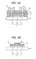
- FIGS. 1B , 5A, and 5Beach illustrate a structural example in which the source electrode 13 and the drain electrode 14 are provided.
- an insulating slayer 19is provided on the structure illustrated in FIG. 1A and the source electrode and the drain electrode are connected with the source part and the drain part through vias.
- a glass substrate, a plastic substrate, a plastic film, or the likecan be used as the substrate 10.
- the channel layer and the gate insulating layer as described aboveare transparent to visible light. Therefore, when a transparent material are used for the electrodes and the substrate, a transparent thin film' transistor can be produced.
- the field effect transistorhas a three-terminal device including the gate electrode 15, the source electrode 13, and the drain electrode 14.
- the field effect transistoris an electronic active device having a function for controlling a current Id flowing into the channel based on a voltage Vg applied to the gate electrode. This enables to control the current Id flowing between the source electrode and the drain electrodes.
- FIGS. 7A and 7Billustrate typical characteristics of the field effect transistor according to this embodiment. While a voltage Vd of approximately 5 V is applied between the source electrode and the drain electrode, the gate voltage Vg to be applied is switched between 0 V and 5 V, the current Id (unit: pA) flowing between the source electrode and the drain electrode can be controlled (switched on/off).
- FIG. 7Aillustrates an example of an Id-Vd characteristic at each Vg and
- FIG. 7Billustrates an example of Id-Vg characteristic (transfer characteristic) at Vd of 6 V.
- the hysteresismeans that, as illustrated in FIGS. 8A and 8B , in the case where a TFT transfer characteristic is evaluated, when Vg is swept (risen and fallen) while Vd is held, a change in value of Id during the rise of the voltage is different from that during the fall of the voltage.
- Vgis swept (risen and fallen) while Vd is held
- a change in value of Id during the rise of the voltageis different from that during the fall of the voltage.
- the hysteresisis large, the value of Id obtained at set Vg varies. Therefore, a device having small hysteresis may be used.
- FIGS. 8A and 8Billustrate examples of the TFT transfer characteristic in the case of a conventional structure in which the source electrode and the drain electrode are directly formed on the oxide film and the TFT transfer characteristic in the case of the structure in this embodiment in which the source part and the drain part, each of which has a high hydrogen concentration, are provided.
- the conventional, structureexhibits the hysteresis characteristic as illustrated in FIG. 8A .
- the device having small hysteresis as illustrated in FIG. 8Bcan be obtained.
- the amount of charges trapped in a connection portionmay be lowered to reduce the hysteresis.
- the field effect transistor described abovecan be manufactured by the following manufacturing method.
- the manufacturing methodincludes a step of forming the oxide film which is the channel layer and a step of adding hydrogen to portions of the oxide film to form the source part and the drain part.
- a method of forming in advance an oxide film having a resistance value suitable to provide the channel part and then adding hydrogen to portions of the oxide film to form the source part and the drain partmay be used.
- a methodmay be used in which an' oxide film having a resistance value slightly smaller than the resistance value suitable to provide the channel part is formed in advance and then a hydrogen concentration of a portion of the oxide film is reduced to form the channel part.
- the former methodis suitable because it is easy to control the hydrogen concentration.
- a sputtering methodSP method
- PLD methodpulse laser deposition method
- an electron beam deposition methodmay be used as a method of forming the oxide film.
- the SP methodis suitable in view of mass productivity.
- the film formation methodis not limited to those methods.
- a temperature of a substrate during film formationcan be held to substantially a room temperature without intentionalheating.
- a method such as hydrogen ion implantation, hydrogen plasma processing, hydrogen atmosphere processing, or diffusion from an adjacent hydrogencontaining filmcan be uses as the method of adding hydrogen to the oxide film.
- the ion implantation methodis suitable in view of the control of a hydrogen content.
- An H + ion, an H - ion, a D + ion (deuterium ion), an H 2+ ion (hydrogen molecular ion), or the likecan be used as an ion species for the ion implantation method.
- the hydrogen plasma processingis suitable in view of throughput.
- the hydrogen plasma processingcan be performed using a parallel-plate type plasma CVD apparatus or an RIE type plasma etching apparatus.
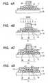
- the source part and the drain parthydrogen is added to the oxide film using the pattern of the gate electrode located above the channel layer as a mask.
- the source part and the drain partcan be formed in self-alignment with the gate electrode.
- the oxide film which is the channel layer 11is formed on the substrate 10 by patterning.
- the gate insulating layer 12is deposited.
- the gate electrode 15is formed by patterning.
- hydrogenis added into the oxide film by a method such as hydrogen ion implantation or hydrogen plasma processing, using the gate electrode as the mask ( FIG. 3A ), thereby forming the source part 16 and the drain part 17 ( FIG. 3B ). After that, annealing may be performed to uniform the hydrogen amount.
- the coplanar transistorcan be easily produced by the self-alignment method of adding hydrogen to the channel layer 11 using the gate electrode 15 as the mask.
- the overlap between the gate electrode and each of the source and drain partscan be reduced.
- the overlapinhibits the high-speed operation of the transistor because the overlap acts as a capacitor, (parasitic capacitor).
- a variation in overlapcauses a variation in transistor characteristic.
- the self-alignment processis used, a parasitic capacitance of the transistor which is caused in an overlap portion between the gate electrode and each of the source and drain parts can be reduced and made uniform. As a result, it is possible to produce a transistor having high drive capability and excellent uniformity.
- the positional relationship among the gate, the source, and the draincan be automatically determined without mask alignment which is likely to cause an error. Because the self-alignment method is used, high-precision mask alignment is unnecessary. A mask alignment margin for allowing an error caused in the mask alignment is also unnecessary, so a size of the device can be reduced.
- the methodcan be performed at a low-temperature process, so the thin film transistor can be formed on the substrate such as the plastic plate or the plastic film.
- the number of etching processes and the number of lift-off processescan be reduced to form the source and the drain. Therefore, electrode-semiconductor connection can be realized in a low-cost process with excellent stability.
- a display devicecan be produced in which the drain corresponding to an output terminal of the field effect transistor is connected with an electrode of a display element such as an organic or inorganic electroluminescent (EL) element or a liquid crystal element.
- a display elementsuch as an organic or inorganic electroluminescent (EL) element or a liquid crystal element.
- a field effect transistorincluding an oxide film (channel layer) 112, a source electrode 113, a drain electrode 114, a gate insulating film 115, and a gate electrode 116 is formed on a base 111.
- the drain electrode 114is connected with an electrode 118 through an interlayer insulating film 117.
- the electrode 118is in contact with a light-emitting layer 119.
- the light-emitting layer 1119is in contact with an electrode 120.
- a current injected into the light-emitting layer 119can be controlled based on a current value flowing between the source electrode 113 and the drain electrode 114 through the channel formed in the oxide film 112.
- the current injected into the light-emitting layer 119can be controlled based on a voltage applied to the gate electrode 116 of the field effect transistor.
- the electrode 118, the light-emitting layer 119, and the electrode 120compose an inorganic or organic electroluminescent element.
- the drain electrode 114is extended to also serve as the electrode 118, so a structure can be provided in which the drain electrode 114 is used as the electrode 118 for applying a voltage to a liquid crystal cell or electrophoresis particle cell 123 sandwiched between high-resistance films 121 and 122.
- the liquid crystal cell or electrophoresis particle cell 123, the high-resistance films 121 and 122, the electrode 118, and the electrode 120compose a display element.
- a voltage applied to the display elementcan be controlled based on a voltagevalue of the drain electrode 114 Therefore, the voltage applied to the display element can be controlled based on a voltage applied to the gate electrode 116 of the TFT.
- a display medium of the display elementis a capsule in which a fluid and particles are sealed in an insulating coating, the high-resistance films 121 and 122 are unnecessary.
- the top-gate coplanar structureis typically shown.
- this embodimentis not necessarily limited to this structure.
- the connection between the drain electrode which is the output terminal of the field effect transistor and the display elementis topologically the same, another structure such as the staggered structure can be employed.
- the example in which the pair of electrodes for driving the display element are provided in parallel with the baseis shown.
- this embodimentis not necessarily limited to such a structure.
- the connection between the drain electrode which is the output terminal of the field effect transistor and the display elementis topologically the same, any one of the electrodes or both the electrodes may be provided perpendicular to the base.
- the field effect transistor shown in the drawingmay be connected with another field effect transistor according to this embodiment. It is only necessary that the field effect transistor illustrated in the drawing be provided at a final stage of a circuit including field effect transistors.
- the pair of the electrodes for driving the display elementare provided in parallel with the base
- the display elementis an EL element or a reflection display element such as a reflection liquid crystal element
- any one of the electrodesbe transparent to the wavelength of emitted light or the wavelength of reflected light.
- a display devicesuch as a transmission-type liquid crystal element
- each of the electrodesbe transparent to transmitted light.
- All members composing the field effect transistor according to this embodimentcan be also made transparent, with the result that a transparent display element can be produced.
- a display elementcan be provided on a low-heat-resistant base such as a resin plastic substrate which is light weight, flexible, and transparent.
- pixelseach of which includes an EL element (organic EL element in this case) and field effect transistors, are two-dimensionally arranged will be described with reference to FIG. 13 .
- a.transistor 181drives an organic EL layer 184 and a transistor 182 selects a pixel.
- a capacitor 183which is used to maintain a selected state and located between a common electrode line 187 and the source portion of the transistor 182 stores charges to.hold a signal applied to the gate of the transistor 181.
- the pixel selectionis determined by a scanning electrode line 185 and a signal electrode line 186.
- an image signalis applied as a pulse signal from a driver circuit (not shown) to a gate electrode through the scanning electrode line 185.
- a pulse signalis applied from another driver circuit (not shown) to the transistor 182 through the signal electrode line 186, thereby selecting a pixel.
- the transistor 182is turned ON to store charges in the capacitor 183 located between the signal electrode line 186 and the source of the transistor 182. Therefore, a gate voltage of the transistor 181 is held to a desirable voltage, so the transistor is turned ON. Such a state is held until a next signal is received.
- a voltage and a currentare being supplied to the organic EL layer 184 to maintain light emission.
- each pixelincludes two transistors and a capacitor. In order to improve the performance, a larger number of transistors and the like may be incorporated. It is essential that an In-Ga-Zn-O'field effect transistor which is the transparent field effect transistor according to this embodiment which can be formed at a low temperature be used for a transistor portion. Therefore, an effective EL element is obtained.
- the top-gate TFT device having the coplanar structure as illustrated in FIG. 1Awas manufactured.
- An amorphous In-Ga-Zn-O oxidewas used for the channel layer 11.
- a hydrogen ion implantation methodwas used to form the source part and the drain part.
- the amorphous oxide film as the channel layer 11was formed on the glass substrate 10 (manufactured by Corning Incorporated, 1737).
- the amorphous In-Zn-Ga-O oxide filmwas formed by radio frequency sputtering under a mixed atmosphere of argon gas and oxygen gas.
- a sputtering apparatus for film formation as illustrated in FIG. 10including a sample 51, a target 52, a vacuum pump 53, a vacuum gauge 54, a substrate holding means 55, gas flow rate control means 56 provided for the respective gas introduction systems, a pressure control means 57, and a film formation chamber 58, was used.
- the sputtering apparatus for film formationwhich includes the film formation chamber 58, the vacuum pump 53 for evacuating the film formation chamber, the substrate holding means 55 for holding the substrate on which the oxide film is formed in the film formation chamber, and the solid material source (target) 52 opposed to the substrate holding means, and further including an energy source (radio frequency power source which is not shown) for evaporating a material from the solid material source, and a means for supplying an oxygen gas into the film formation chamber.
- the energy sourceradio frequency power source which is not shown
- a polycrystalline sintered material having a composition of InGaO 3 (ZnO) having a size of two incheswas used as the target (material source), and the applied RF power was 100 W.
- the film formation ratewas 13 nm/min, and the temperature of the substrate was 25°C.
- the electrical conductivitywas approximately 10 -2 S/cm
- the electron carrier concentrationwas 4 ⁇ 10 16 /cm 3
- the estimated electron mobilitywas approximately 2 cm 2 /V ⁇ sec.
- forbidden band energy width of the manufactured amorphous oxide filmwas approximately 3 eV.
- the gate insulating layer 12was formed by patterning using a photolithography method and a lift-' off method.
- the gate insulating layerwas obtained by forming a Y 2 O 3 film at a thickness of 150 nm using an electron beam deposition method.
- a relative dielectric constant of the Y 2 O 3 filmwas approximately 15.
- the gate electrode 15was formed using a photolithography method and a lift-off method.
- the channel length thereofwas 90 ⁇ m while the channel width thereof was 200 ⁇ m.
- the electrodewas made of Au and had a thickness of 30 nm.
- hydrogen (or deuterium) ionwas implanted to the amorphous oxide thin film ( FIG. 3A ) to form the source part and the drain part in the channel layer ( FIG. 3B ).
- hydrogen ionswere implanted into the channel layer through the gate insulating layer.
- the gate electrodewas used as a mask and the source part and the drain part were arranged in self-alignment corresponding to the pattern of the gate electrode.
- H +proton
- accelerating voltage20 kV
- An ion irradiation amount per areawas able to be set to approximately 1x10 13 (1/cm 2 ) to 1x10 17 (1/cm 2 ).
- a specimen to which deuterium ions D + are implantedwas separately prepared as in the above-mentioned case.
- Composition analysiswas performed using a SIMS to evaluate a hydrogen content.
- a hydrogen concentration of a thin film of a specimen irradiated with ions at 1 ⁇ 10 15 (1/cm 2 )was approximately 2 ⁇ 10 19 (1/cm 3 ) Therefore, for example, in the case of a specimen in which an ion irradiation amount was 1 ⁇ 10 13 (1/cm 2 ), a hydrogen concentration was not able to be measured because it was equal to or smaller than the detection limit. However, it was able to be evaluated that the hydrogen concentration was approximately 2 ⁇ 10 17 (1/cm 3 ).
- the hydrogen ion irradiation amount of each of the source part and the drain part in the thin film transistor according to this examplewas set to 1 ⁇ 10 16 (1/cm 2 ).
- the hydrogen concentrationwas evaluated to be approximately 2 ⁇ 10 20 (1/cm 3 ).
- Electric conductivity of a specimen separately preparedwas evaluated. The electric conductivity was approximately 80 S/cm.
- each of the source part and the drain parthad sufficient high electric conductivity, so that the structure illustrated in FIG. 1A with omitting a source electrode and a drain electrode was employed.
- a device having a structure in which a source electrode and a drain electrode were directly formed on an oxide filmwas produced.
- An amorphous oxide layerwas formed on a substrate.
- the source electrode, the drain electrode, a gate insulating layer, and a gate electrodewere formed by patterning.
- the self-alignment methodwas not used.
- the formation of each layerwas performed based on Example 1.
- An Au electrode having a thickness of 30 nmwas used as each of the source electrode and the drain electrode. Evaluation of Characteristics of TFT Device
- FIGS. 7A and 7Billustrate exemplary current-voltage characteristics of the TFT device measured at a room temperature.
- FIG. 7Aillustrates the Id-Vd characteristics
- FIG. 7Billustrates the Id-Vg characteristics.
- Vgwhen predetermined gate voltage Vg was applied and the dependence of the source-drain current Id on the drain voltage Vd along with variation of Vd was measured, behavior of a typical semiconductor transistor, i.e., saturation (pinch off) at a time when Vd was approximately 6V, was exhibited.
- the threshold value of the gate voltage V Gwas approximately -0.5 V.
- Vgwas 10 V
- the current Idapproximately 1.0 ⁇ 10 -5 A flew.
- the on/off ratio of the transistorwas 10 6 or more. Further, when the field effect mobility was calculated from the output characteristics, the field effect mobility of approximately 8cm 2 (Vs) -1 was obtained in a saturation region. The manufactured device was irradiated with visible light and the same measurement was made. No change in the transistor characteristics was observed.
- a variation in characteristics of a plurality of the devices produced on the same substratewas evaluated.
- the variation in this examplewas smaller than that in the comparative example.
- a variation in on-currentswas evaluated.
- the variationwas approximately ⁇ 15% in the comparative example. In contrast to this, the variation was approximately ⁇ 10% in this example.
- the channel layerincluded the channel part, and the source part and the drain part, each of which had a hydrogen concentration larger than that of the channel part. Therefore, it is expected that stable electrical connection was able to be made between the channel part and each of the source electrode and the drain electrode, thereby improving the uniformity and reliability of the device.
- the TFT according to this examplehad hysteresis smaller than that of the TFT of the comparative example.
- FIGS. 8A and 8Billustrate the Id-Vg characteristics in this example and the comparative example for comparison therebetween.
- FIG. 8Aillustrates the comparative example
- FIG. 8Billustrates the example of the TFT characteristics in this example.
- hydrogenwas added to the channel layer, the hysteresis of the TFT was able to be reduced.
- the satisfactory electrical connection which was resistant to trap chargeswas able to be realized between each of the source and drain electrode and the channel, so the thin film transistor having small hysteresis was able to be realized.
- the positional relationship among the gate, the source; and the drainwas able to be realized with high precision by the self-alignment method.
- high-speed operationwas possible and the device having high uniformity was able to be realized.
- the field effect transistor having a relatively large field effect mobilityaccording to this example be used for, for example, a circuit for operating an organic light emitting diode.
- Example 1a structure and a manufacturing method were based on Example 1. However, a hydrogen implantation amount was controlled such that the hydrogen concentration of each of the source part and the drain part became approximately 1x10 18 (1/cm 3 ).
- the insulating layer 19When the relatively low hydrogen concentration was applied to the source part and the drain part, the insulating layer 19, the source electrode, and the drain electrode were further provided.as illustrated in FIG. 5A , so that the satisfactory transistor characteristics was able to be realized as in the case of Example 1.
- the hysteresis characteristic, the uniformity, and the high-speed operation performancewere also preferable.
- This exampleis an example in which the bottom-gate TFT device having the coplanar structure as illustrated in FIG. 1B was manufactured.
- the devicewas produced using the manufacturing method illustrated in FIGS. 4A to 4D .
- the self-alignment methodwas not used.
- a channel layer made of amorphous In-Ga-Zn-O oxidewas formed using a PLD method.
- the source part and the drain partwere formed using hydrogen plasma processing.
- the gate electrode 15was patterned using a photolithography method and a lift-off method on a glass substrate 10 (manufactured by Corning Incorporated, 1737).
- the electrodewas made of Ta and had a thickness of 50 nm.
- the gate insulating layer 12was formed by patterning using a photolithography method and a lift-off method.
- the gate insulating layerwas obtained by forming an HfO 2 film in a thickness of 150 nm using a laser deposition method.
- an amorphous In-Zn-Ga-O oxide film which is the channel layerwas formed by patterning using a photolithography method and a lift-off method.
- An amorphous In-Zn-Ga-O oxide filmwas deposited by a PLD method using a KrF excimer laser.
- the amorphous In-Zn-Ga-O oxide filmwas deposited with using a polycrystalline sintered material having a composition of InGaO 3 (ZnO) 4 as the target.
- the oxygen partial pressure when the film was formedwas 7 Pa.
- the power of the KrF excimer laserwas 1.5 ⁇ 10 -3 mJ/cm 2 /pulse, the pulse width was 20 nsec, and the repetition frequency was 10 Hz. Further, the temperature of the substrate was 25°C.
- XRFX-ray fluorescence
- a resist mask 20 having the same pattern as that of the gate electrodewas formed by patterning ( FIG. 4A ).
- hydrogenwas added to the amorphous In-Ga-Zn-O thin film which was the channel layer by hydrogen plasma processing using a plasma processing apparatus.
- the hydrogen plasma processingcan be performed using a parallel-plate type plasma CVD apparatus or an RIE type plasma etching apparatus ( FIG. 4B ).
- a specimen to be processed(substrate obtained after the above step) was stored in the apparatus which was evacuated. After that, a gas containing hydrogen was introduced from a reactive gas introduction port and radio frequency power was introduced into a processing container by a radio frequency (RF) power source, thereby generating plasma.
- RFradio frequency
- an electrode intervalwas set to 5 cm
- a substrate temperaturewas set to 100°C
- an H 2 gas flow ratewas set to 500 sccm
- an inner pressure of the chamberwas set to 1 Torr.
- a hydrogen content of the thin film subjected to the hydrogen plasma processingincreased and a resistivity thereof reduced.
- each of the electrodeswas made of gold and had a thickness of 30 nm ( FIG. 4C ).
- a channel lengthwas 50 ⁇ m and a channel width was 180 ⁇ m.
- Example 2A specimen not subjected to the above-mentioned hydrogen plasma processing was prepared. That is, the channel layer had a substantially uniform hydrogen concentration over the entire film region thereof and did not include the source part and the drain part. Other structures and manufacturing methods were based on Example 2.
- An on/off ratio of the transistorwas 10 6 or more and a field effect mobility thereof was approximately 7 cm 2 (Vs) -1 .
- the channel layerincluded the channel part, and the source part and the drain part, each of which had a hydrogen concentration larger than that of the channel part. Therefore, it is expected that stable electrical connection was able to be made between the channel part and each of the source electrode and the drain electrode, thereby improving the uniformity and reliability of the device.
- the field effect transistor having a relatively large field effect mobilityaccording to this example be used for, for example, a circuit for operating an organic light emitting diode.
- This exampleis an example in which a top-gate TFT device as illustrated in FIG. 5B was formed on a plastic substrate.
- PETpolyethylene terephthalate
- a channel layerwas formed'on the substrate, by patterning.
- a polycrystalline sintered material having a composition of In 2 O 3 /ZnO having a size of two incheswas used as the target (material source), and the applied RF power was 100 W.
- the film formation ratewas 12 nm/min, and the temperature of the substrate was 25°C.
- the gate insulating layer and the gate electrodeare formed to be the same pattern.
- the gate electrodeis a transparent conductive film composed of In 2 O 3 :Sn.
- Example 3hydrogen plasma processing was performed as in the case of Example 3.
- the source part 16 and the drain part 17were formed in.self-alignment using the gate electrode as a mask.
- a source electrode and a drain electrodewere formed by patterning.
- a transparent conductive film composed of In 2 O 3 :Snwas used as each of the source electrode and the drain electrode and a thickness thereof was 100 nm.
- the TFT formed on the PET filmwas measured at a room temperature.
- An on/off ratio of the transistoris 10 3 or more.
- Calculated field effect mobilitywas approximately 3 cm 2 (Vs) -1 .
- Vscm 2
- the transistor characteristicwas measured in the same manner. A large change in transistor characteristic was not observed. The same measurement was performed with visible irradiation. A change in transistor characteristic was not observed.
- the thin film transistor produced in this embodimentwas transparent to visible light and formed on a flexible substrate.
- a display device using the field effect transistor illustrated in FIG. 12will be described.
- the field effect transistoran island of an ITO film serving as the drain electrode was extended from a short side thereof up to 100 ⁇ m. A portion corresponding to 90 ⁇ m of an extended portion was left to ensure wirings for the source electrode and the gate electrode. Then, the TFT was coated with an insulating layer. A polyimide film was applied onto the insulating layer and subjected to a rubbing step. On the other hand, a plastic substrate in which an ITO film and a polyimide film were formed thereon and a rubbing step was performed was prepared.
- the plastic substratewas opposed to the substrate on which each field effect transistor was formed at a gap of 5 ⁇ m and then nematic liquid crystal was injected thereto.
- a pair of polarizing plateswere provided on both sides of such a structure.
- a white plastic substratewas used as the substrate on which each TFT was formed.
- a material of each of the electrodes of the TFTwas replaced by gold.
- the polyimide film and the polarizing plateswere omitted.
- a gap between the white plastic substrate and the transparent plastic substratewas filled with capsules in which particles and a fluid were coated with an insulating coating.
- a voltage between the extended drain electrode and the ITO film located thereabovewas controlled by the field effect transistor, so that the particles in the capsules move in the longitudinal direction. Therefore, the reflectance of the extend drain region as viewed from the transparent substrate side was able to be controlled for display.
- a plurality of field effect transistorwere formed adjacent to one another to produce, for example, a normal current control circuit including four transistors and a capacitor. Therefore, the TFT illustrated in FIG. 11 was able to be used as one of final-stage transistors to drive an EL element.
- the field effect transistor using the ITO film as the drain electrodewas employed.
- An organic electroluminescence element including a charge injecting layer and a light emitting layerwas formed in the region of 30 ⁇ m ⁇ 90 ⁇ m which was the portion of the island of the ITO film which was extended from the drain electrode.
- the display device using the EL elementwas able to be produced.
- Display elements and field effect transistorseach of which corresponds to that in Example 5, were two-dimensionally arranged.
- 7425 ⁇ 1790 pixelseach of which included the display element such as the liquid crystal cell or the EL element and the field effect transistor in Example 5 and had an area of 30 ⁇ m ⁇ 115 ⁇ m; were arranged in a square shape at a pitch of 40 ⁇ m in a short-side direction and at a pitch of 120 ⁇ m in a long-side direction.
- 1790 gate wirings passing through the gate electrodes of 7425 field effect transistors in the long-side directionwere provided and 7425 signal wirings passing through portions of the source electrodes of 1790 TFTs which protrude from amorphous oxide semiconductor film islands by 5 ⁇ m in the short-side direction were provided.
- the wiringswere connected with a gate driver circuit and a source driver circuit.
- the gate electrode of a first field effect transistorwas connected with a gate line and the source electrode of a second field effect transistor was connected with signal line.
- the light emission wavelengths of the EL elementswere repeated in the order of R, G, and B lights in the long-side direction. Therefore, a light-emission color image display device having the same resolution was able to be constructed.
- a driver circuit for driving an active matrix circuitmay be constructed using the TFT according to this embodiment which is identical to the field effect transistor of the pixel or constructed using an existing IC chip.
- the field effect transistor according to the present inventioncan be formed on the flexible material including the PET film. That is, switching can be performed with a bending state.
- the field effect transistoris transparent to visible light and infrared light which have a wavelength of 400 nm or more, so that the field effect transistor according to the present invention can be applied as a switching element of an LCD or an organic EL display.
- the field effect transistor according to the present inventioncan be widely applied to a flexible display, a see-through display, an IC card, an ID tag, and the like.
- the channel layerincludes the source part and the drain part which are added with hydrogen or deuterium.
- the channel layer (oxide film)includes the channel part containing hydrogen.or deuterium and the source part and the drain part which have the hydrogen concentration larger than that .of the channel part. Therefore, the stable electrical connection can be made between the channel part and each of the source electrode and the drain electrode, thereby improving the uniformity and reliability of the device.
- the satisfactory'electrical connection resistant to trap chargescan be realized between each of the source and drain electrode and.the channel, so that the field effect transistor having small hysteresis and excellent characteristic stability can be realized.
- the source part and the drain partcan be formed in self-alignment with the pattern of the gate electrode, with the result that the positional relationship among the gate, the source, and the drain can be realized with high precision.
Landscapes
- Thin Film Transistor (AREA)
- Liquid Crystal (AREA)
- Electroluminescent Light Sources (AREA)
- Dram (AREA)
Abstract
Description
- The present invention relates to a field effect transistor including an oxide film as a semiconductor layer, a method of manufacturing the same, and a display device. In particular, the present invention relates to a field effect transistor having transistor characteristics which can be applied to a display device or the like, a method of manufacturing the same, and a display device.
- A field effect transistor (FET) is a three-terminal device having a gate electrode,a source electrode, and a drain electrode. Further, the field effect transistor is an electronic active device in which a current flowing through a channel layer (a current between a source electrode and a drain electrode) is controlled by voltage applied to a gate electrode.. In particular, an FET which uses as a channel layer a thin film is called a thin film FET (thin film transistor, TFT). The device can be formed on an several substrates formed of ceramic, glass, plastic, or the like.
- The above-mentioned TFT has an advantage of being easily formed on a substrate having a relatively large area because the TFT uses thin film technology, and is widely used as a driving device in a flat panel display device such as a liquid crystal display device. More specifically, in an active liquid crystal display (ALCD), TFTs formed on a glass substrate are used to turn on and off individual image pixels. Also, in a prospective high performance organic LED display (OLED), it is thought to be effective to current-drive the pixels by TFTs. Further, a higher performance liquid crystal display device is realized in which a TFT circuit having a function of driving and controlling the whole image is formed on a substrate in the vicinity of an image display region.
- A TFT which is currently most widely used is a metal-insulator-semiconductor field effect transistor (MIS-FET) device using a polycrytalline silicon film or an amorphous silicon film as a channel layer material. An amorphous silicon TFT is practically used for pixel driving and a high-performance polycrystalline silicon TFT is practically used for drive control of the entire image.
- However, it is difficult to form the amorphous silicon TFT and the polycrystalline silicon TFT on a substrate such as a plastic plate or a plastic film because a high-temperature process is essential for device formation.
- In recent years, active development has been conducted for realizing a flexible display by using TFTs formed on a substrate such as a polymer plate or a polymer film for a driver circuit of an LCD or OLED. Attention is focused on an organic semiconductor film which is made of a material capable of being formed on a plastic film or the like, which can be formed at a low temperature.
- For example, pentacene has been under research and development for the organic semiconductor film. The organic semiconductor has an aromatic ring. Large carrier mobility is obtained in the stack direction of the aromatic ring at the time of crystallization. For example, it is reported that, in the case where the pentacene is used for an active layer, the carrier mobility is approximately 0.5 cm2(Vs)-1, which is equal to that of an amorphous SI-MOSFET.
- However, the organic semiconductor such as the pentacene has low thermal stability (it is unstable when temperature exceeds 150°C) and toxicity (carcinogenicity). Therefore, a practical device has not been realized.
- Attention has been recently focused on an oxide material as a material which can be applied to the channel layer of a TFT.
- four example, a TFT using, as the channel layer thereof, a transparent conductive oxide polycrystalline thin film containing ZnO as a main ingredient has been under active development. The thin film can be formed at a relatively low temperature, and therefore it is possible to form the film on a substrate such as a plastic plate or a plastic film. However, in the case of a compound containing ZnO as a main ingredient, a stable amorphous phase cannot be formed at a room temperature and a polycrystalline phase is formed. Therefore, it is difficult to increase an electron mobility thereof because of scattering of polycrystalline grain boundaries. In addition,' it is difficult to achieve reproductivity in the characteristics of a TFT device because a' polycrystalline grain shape and an interconnection thereof are significantly changed depending on film formation methods.
- A thin film transistor using an amorphous In-Ga-Zn-O-based oxide has been reported byK. Nomura, et al., Nature, 432, 488 (2004). The thin film transistor can be formed on a plastic plate or a glass substrate at a room temperature. The device shows a normally-off characteristics with field effect mobility of approximately 6 to 9. There is also an advantage in that the thin film transistor is transparent to visible light.
WO 2004/114391 A andUS 2006/0244107 A disclose a thin-film transistor where the active layer is formed of zinc oxide or magnesium zinc oxide.- The inventors of the present invention have studied a thin film transistor using an oxide including an amorphous In-Ga-Zn-O oxide. As a result, there is the case where a variation in transistor characteristic (Id-Vg characteristic) of a TFT occurs, although an extent of the variation is depended on the channel materials or the manufacturing conditions etc.
- When the TFT is used for, for example, a pixel circuit of a display, the variation in characteristic causes a variation in operation of an organic LED or a liquid.crystal element which is to be driven, therevy finally reducing the image quality of the display.
- In view of the above, an object of the present invention is to reduce the above-mentioned variation in characteristic.
- Examples of a factor of the variation include:
- 1) a parasitic resistance caused between each of source and drain electrodes and a channel; and
- 2) a variation in positional relationship among a. gate, a source, and a drain.
- Specifically, a first object of the present invention is to device a connection between the channel of a transistor and each of the source and drain electrodes thereof, thereby reducing the variation in characteristic.
- A second object of the present invention is to provide a structure capable of forming the positional relationship among the gate, the source, and the drain with high precision and a manufacturing method thereof, thereby reducing the variation in characteristic.
- In view of these objects, the present invention provides the field effect transistor claimed in
claim 1, the display device claimed inclaim 10, and the method of manufacturing a field effect transistor claimed inclaim 12. - The other claims relate to further developments.
FIGS. 1A and 1B are cross sectional views illustrating structural examples of a field effect transistor according to the present invention;FIG. 2 is a diagram illustrating a change in resistivity of amorphous In-Ga-Zn-O oxide film in a case where hydrogen is added thereto;FIGS. 3A and 3B are cross sectional views illustrating a method of manufacturing a field effect transistor according to the present invention with using a self-alignment method;FIGS. 4A, 4B, 4C and 4D are cross sectional views illustrating a method of manufacturing a field effect transistor according to the present invention;FIGS. 5A and 5B are cross sectional views illustrating structural examples of a field effect transistor according to the present invention;FIG. 6 is a cross sectional view illustrating a structural example of a field effect transistor according to the present invention;FIGS. 7A and 7B are graphs illustrating TFT characteristics of a field effect transistor according to the present invention;FIGS. 8A and 8B are graphs illustrating a hysteresis characteristic of the field effect transistor according to the present invention;FIG. 9 is a graph illustrating a relationship between electric conductivity of an amorphous In-Ga-Zn-O oxide film and an oxygen partial pressure during film formation;FIG. 10 is a cross sectional view illustrating an apparatus for forming the amorphous oxide film;FIG. 11 is a cross sectional view illustrating an example of a display device according to the present invention;FIG. 12 is a cross sectional view illustrating another example of a display device according to the present invention; andFIG. 13 is a diagram illustrating a structure of a display device in which pixels each including an organic EL device and a thin film transistor are two-dimensionally arranged.FIGS. 1A and 1B are cross sectional views illustrating structural examples of a field effect transistor according to an embodiment of the present invention.FIG. 1A illustrates an example of a top-gate structure andFIG. 1B illustrates an example of a bottom-gate structure.- In
FIGS. 1A and 1B , provided are on asubstrate 10, a channel layer (oxide thin film) 11, agate insulating layer 12, asource electrode 13, adrain electrode 14, agate electrode 15, asource part 16, adrain part 17, and achannel part 18. Thechannel layer 11 includes thesource part 16, thedrain part 17, and thechannel part 18. - As illustrated in
FIG. 1A , thegate insulating layer 12 and thegate electrode 15 are formed on thechannel layer 11 in mentioned order, thereby obtaining the top-gate structure. As illustrated inFIG. 1B , thegate insulating layer 12 and thechannel layer 11 are formed on thegate electrode 15 in mentioned order, thereby obtaining the bottom-gate structure. InFIG. 1A , the source part and the drain part also serve as the source electrode and the drain electrode, respectively. InFIG. 1B , the channel part of the transistor and the source electrode (drain electrode) are connected with each other through the source part (drain part). - As illustrated in each of
FIGS. 1A and 1B , in the field effect transistor (FET) according to this embodiment, the oxide thin film which is thechannel layer 11 includes thechannel part 18, thesource part 16, and thedrain part 17. Thesource part 16 and thedrain part 17 are added with hydrogen or deuterium to reduce a resistivity thereof. When thechannel part 18 contains hydrogen or deuterium, the concentration of hydrogen or deuterium of each of thesource part 16 and thedrain part 17 is set to a value larger than the concentration of hydrogen or deuterium of thechannel part 18. There are the case where hydrogen or deuterium is actively added to thechannel part 18 and the case where hydrogen is contained therein without adding hydrogen actively. As described later, the electric conductivity of the source part (drain part) can be increased by the addition of hydrogen or deuterium thereto. In addition, when the concentration of hydrogen or deuterium of the source part (drain part) is increased to a value larger than the concentration of hydrogen or deuterium of thechannel part 18, the electric conductivity of the source part (drain part) can be set to a value larger than the electric conductivity of the channel part. According to the structure, the channel part and the source (drain) electrode can be electrically connected with each other with high reliability, whereby a thin film transistor having small variation can be realized. - In particular, according to this embodiment, the source part and the drain part are formed in the oxide film. Therefore, stable electrical connection can be made in comparison with the case of a conventional structure in which the source electrode and the drain electrode are directly formed on the oxide film.
- In this embodiment, a top-gate structure, a bottom-gate structure, a staggered structure, or a coplanar structure can be arbitrarily used as the structure of the field effect transistor. In view of the stable electrical connection, the coplanar structure illustrated in
FIG. 1A may be used. When the coplanar structure is used, the source and drain electrodes are directly connected with an interface between the gate insulating layer and the channel layer, and high-reliability electrical connection can be attained. - The transistor according to this embodiment may have a structure in which the gate electrode and the source (drain) part are formed in self-alignment. That is, as described later, hydrogen is added to the oxide film by using a pattern of the gate electrode as a mask, whereby the source part and the drain part in self-alignment with respect to the pattern of the gate electrode are formed in the oxide film.
- When the self-alignment method is used, a transistor can be realized in which the overlap between the source (drain) part and the gate electrode is small and uniform. As a result, a parasitic capacitance of the transistor which is caused in an overlap portion' between the gate electrode and the drain part can be reduced and made uniform. Because of the small parasitic capacitance, high-speed operation can be realized. Because of the uniform parasitic capacitance, a transistor excellent in uniform characteristics is can be realized.
- As described earlier, the
source part 16 and thedrain part 17 are added with hydrogen or deuterium to reduce resistivity thereof. The inventors of the present invention found that, when hydrogen (or deuterium) is added to an amorphous In-Ga-Zn-O thin film, the electric conductivity of the oxide thin film becomes larger. In the case that thechannel part 18 contains hydrogen or deuterium, the concentration of hydrogen or deuterium of each of the source part and the drain part is increased to a value larger than the concentration of hydrogen or deuterium of the channel part, so electrical connecting can be improved. FIG. 2 is a characteristic graph illustrating an example of a relationship between a hydrogen ion implantation amount and resistivity.FIG. 2 illustrates a change in electric conductivity to the hydrogen ion implantation amount in the case where ions are implanted into an InGaZnO4 thin film having a film thickness of approximately 500 nm. The abscissa (x-axis) is a logarithmic representation of the hydrogen ion implantation amount per unit area and the ordinate (y-axis) is a logarithmic representation of the resistivity. Therefore, hydrogen can be added to the amorphous oxide film to control the electric conductivity.- When hydrogen or deuterium is added to the source part and the drain part, the electric conductivity thereof can be increased. When the channel part contains hydrogen or deuterium, the concentration of hydrogen of each of the source part and the drain part is increased to a value larger than the concentration of hydrogen of the channel part. Therefore, the electric conductivity of each of the source part and the, drain part can be set to a value larger than the electric conductivity of the channel part. As described above, when each of the source part and the drain part is made of a material substantially identical (except for the hydrogen concentration) to that of the channel part, satisfactory electrical connection between the channel part and each of the source electrode and the drain electrode can be realized. That is, the source (drain) electrode is connected with the channel part through the source (drain) part, thereby realizing the satisfactory electrical connection.
- In this embodiment, any resistivity that is smaller than the resistivity of the channel part can be used as the resistivity of each of the source part and the drain part. The resistivity of each of the source part and the drain part may be equal to or smaller than 1/10 of the resistivity of the channel part. When the resistivity of each of the source part and the drain part becomes equal to or smaller than 1/1000 of the resistivity of the channel part, the source (drain) part can be used as the source (drain) electrode.
- The amount of change in resistivity to a change in hydrogen concentration depends on a composition of the oxide film, film quality thereof, or the like. For example, when hydrogen ions of approximately 1017 (1/cm3) per volume are implanted into an In-Ga-Zn-O thin film having approximately 1000 Ωcm, the resistivity thereof can be reduced to approximately several 50 Ωcm. When hydrogen ions of approximately 1019 (1/cm3) are implanted, the resistivity can be reduced to approximately 0.5 Ωcm. A concentration range of the hydrogen added to each of the source part and drain part depends on a structure of the oxide film, but a concentration may be equal to or larger than 1017 /cm3. In particular, when a concentration equal to or larger than approximately 1019 /cm3 is set, the electric conductivity of each of the source part and the drain part becomes larger, so the source part and the drain part can be used as the source electrode and the drain electrode.
- As described above, depending on a film formation condition, the oxide film may contain hydrogen without active hydrogen addition in some cases. Therefore, there is the case where the channel part contains hydrogen without adding hydrogen actively. Even in such a case, in order to form the source part and the drain part, hydrogen is added in a post-process such that a hydrogen amount which exceeds the amount of hydrogen contained in the channel part is introduced into the source part and the drain part. Therefore, the structure and the effect as described above can be realized.
- A method of locally reducing a hydrogen amount in a portion of the oxide film may also be employed, to use the portion as the channel part.
- The concentration of hydrogen can be evaluated by the measurement using SIMS (secondary ion mass spectrometry). Depending on an evaluation apparatus, a detection limit is approximately 1017/cm3. A value equal to or smaller than the detection limit can be indirectly calculated by an extrapolation based on a linear relationship between a hydrogen addition process parameter (oxygen partial pressure at the time of film formation or ion implantation amount as described later) and the amount of hydrogen contained in the thin film.
- In each of
FIGS. 1A and 1B , the single source part and the single drain part are formed. As illustrated inFIG. 6 ,multiple source parts multiple drain parts source parts drain parts channel part 18, thesource part 16a, and thesource part 16b. Further, the electric conductivity may increase in order of thechannel part 18, thedrain part 17a, and thedrain part 17b. To obtain such a structure, it is only necessary to increase the additional amount of hydrogen ion in order of thechannel part 18, thesource part 16a, and thesource part 16b and to increase the additional amount of hydrogen in order of thechannel part 18, thedrain part 17a, and thedrain part 17b. - Any material that is oxide can be used as the material of the channel layer (oxide file) Examples of the material include In oxide and Zn oxide from which a large mobility can be obtained. Further, the channel layer is made of amorphous oxide. When the following amorphous oxide film is added with hydrogen, the electric conductivity can be effectively increased.
- In particular, components of the channel layer made of amorphous oxide are represented by [(Sn1-xM4x)O2]a· [(In1-yM3y)2O]b· [(Zn1-zM2zO)]c where 0≤x≤1, 0≤y≤1, 0≤z≤1, 0≤a≤1, 0≤b≤1, 0≤c≤1, and a+b+c = 1, M4 is a group VI element (Si, Ge, or Zr) having an atomic number smaller than that of Sn, M3 is Lu or a group III element (B, A1, Ga, or Y) having an atomic number smaller than that of In, and, M2 is a group II element (Mg or Ca) having an atomic number smaller than that of Zn.
- In particular, [(In1-yGay)2O3]b· [(ZnO)]c (where 0≤y≤1, 0≤b≤1, and 0≤c≤1) and [SnO2]a·[(In2O3)]b·[(ZnO)]c (where 0≤a≤1, 0≤b≤1, and 0≤c≤1) are preferable.
- For example, the amorphous oxide film can be realized based on a unary, binary, or ternary composition located in an inner region of a triangle in which SnO2, In2O3, and ZnO are set in vertices. Depending on a composition ratio of the ternary composition, there is the case where crystallization is made in a composition ratio range. For example, with respect to the binary composition including two of three kinds of compounds as described above (composition located in a side of the triangle), an amorphous In-Zn-O film can be formed with a composition in which In is contained therein at equal to or more than approximately 80 atomic% or more and an amorphous Sn-In-O film can be formed with a composition in which In is contained therein at approximately 80 atomic%.
- Further, an amorphous oxide may contain In, Ga, and Zn.
- The inventors of the present invention studied a thin film transistor in which the amorphous oxide is applied to the channel layer. As a result of the study, it is found that a semi-insulating amorphous oxide film having an electric conductivity of 10 S/cm or more and 0.0001 S/cm or less may be applied to the channel, in order to obtain excellent TFT characteristics. Depending on a material composition of the channel, in order to obtain the electric conductivity, an amorphous oxide film may be formed which has an electron carrier concentration of approximately 1014 to 1018 /cm3.
- When the electrical conductivity is 10 S/cm or more, a norinally-off transistor can not be formed, and the on/off ratio can not be made large. In extreme cases, even if gate voltage is applied, the current between the source and drain electrodes is not switched on/off, and transistor operation is not observed.
- On the other hand, in the case of an insulator, in other words, when the electrical conductivity is equal to or less than 0.0001 S/cm, the on-current can not be made large. In extreme cases, even if gate voltage is applied, the current between the source and drain electrodes is not switched on/off, and transistor operation is not observed.
- For example, the electrical conductivity of an oxide used for the channel layer can be controlled by controlling the oxygen partial pressure at the time of forming the film. More specifically, by controlling the oxygen partial pressure, the amount of oxygen vacancy in the thin film is mainly controlled, whereby the electron carrier concentration is controlled.
FIG. 9 is a diagram illustrating exemplary dependence of the electrical conductivity on the oxygen partial pressure when an In-Ga-Zn-O oxide thin film is formed by sputtering. In reality, by highly controlling the oxygen partial pressure, a semi-insulating film which is an amorphous oxide film with a semi-insulating property having an electron carrier concentration of 1014 to 1018/cm3 can be obtained. By using the thin film as described above for the channel layer, a satisfactory TFT can be formed. As illustrated inFIG. 9 , by forming a film with an oxygen partial pressure of typically approximately 0.005 Pa, a semi-insulating thin film can be obtained. When the oxygen partial pressure is 0.001 Pa or less, the formed thin film is insulating, while, when the oxygen partial pressure is 0.01 Pa or more, the electrical conductivity is so high that the film is inappropriate for a channel layer of a transistor. - Several amorphous oxide films, formed in different oxygen partial pressures, were prepared and their transport properties were compared. in a film formation atmosphere is adjusted to evaluate an electron transport properties When the oxygen partial pressure increases, there is the tendency to increase broth the carrier concentration and the electron mobility. Hall mobility measurement is employed for the evaluation.
- In the case of a general semiconductor of Si, GaAs, ZnO etc., when the carrier concentration increases, the electron mobility reduces due to, for example, the interaction among carriers and dopant. On the other hand, in the case of the amorphous oxide film used in this embodiment, the electron mobility increases with an increase in electron carrier concentration. When a voltage is applied to the gate electrode, electrons can be implanted into the channel layer of the amorphous oxide. Therefore, a current flows between the source electrode and the drains electrode, an on-state is obtained between both the electrodes. In the case of the amorphous oxide film in this embodiment, when the electron carrier concentration increases, the electron mobility becomes larger, so a current flowing into the transistor which is in the on-state can be made larger. That is, a saturation current and an on/off ratio can be made larger.
- In the case of the field effect transistor according to this embodiment, any material that has a satisfactory insulating property can be used for the
gate insulating layer 12. For example, Al2O3, Y2O3, HfO2, or a mixed compound including at least two of those compounds can be used for thegate insulating layer 12. Therefore, each of a leak current flowing between the source electrode and the gate electrode and a leak current flowing between the drain electrode and the gate electrode can be reduced to.approximately 10-7 amperes. - Any material that has satisfactory electric conductivity and can make electrical connection with the
source part 16 and thedrain part 17 can be used for each of thesource electrode 13, thedrain electrode 14. Any material can be also used for thegate electrode 15. For example, a transparent conductive film composed of In2O3: Sn, ZnO, or the like or a metal film composed of Au, Pt, Al, Ni, or the like may be used. - When each of the gate part and the drain part has sufficient electric conductivity, the electrodes can be omitted as illustrated in
FIG. 1A . FIGS. 1B ,5A, and 5B each illustrate a structural example in which thesource electrode 13 and thedrain electrode 14 are provided. InFIG. 5A , an insulatingslayer 19 is provided on the structure illustrated inFIG. 1A and the source electrode and the drain electrode are connected with the source part and the drain part through vias.- A glass substrate, a plastic substrate, a plastic film, or the like can be used as the
substrate 10. - The channel layer and the gate insulating layer as described above are transparent to visible light. Therefore, when a transparent material are used for the electrodes and the substrate, a transparent thin film' transistor can be produced.
- The field effect transistor has a three-terminal device including the
gate electrode 15, thesource electrode 13, and thedrain electrode 14. The field effect transistor is an electronic active device having a function for controlling a current Id flowing into the channel based on a voltage Vg applied to the gate electrode. This enables to control the current Id flowing between the source electrode and the drain electrodes. FIGS. 7A and 7B illustrate typical characteristics of the field effect transistor according to this embodiment. While a voltage Vd of approximately 5 V is applied between the source electrode and the drain electrode, the gate voltage Vg to be applied is switched between 0 V and 5 V, the current Id (unit: pA) flowing between the source electrode and the drain electrode can be controlled (switched on/off).FIG. 7A illustrates an example of an Id-Vd characteristic at each Vg andFIG. 7B illustrates an example of Id-Vg characteristic (transfer characteristic) at Vd of 6 V.- Reduction in hysteresis which.is one of effects in this embodiment will be described with reference to
FIGS. 8A and 8B . The hysteresis means that, as illustrated inFIGS. 8A and 8B , in the case where a TFT transfer characteristic is evaluated, when Vg is swept (risen and fallen) while Vd is held, a change in value of Id during the rise of the voltage is different from that during the fall of the voltage. When the hysteresis is large, the value of Id obtained at set Vg varies. Therefore, a device having small hysteresis may be used. FIGS. 8A and 8B illustrate examples of the TFT transfer characteristic in the case of a conventional structure in which the source electrode and the drain electrode are directly formed on the oxide film and the TFT transfer characteristic in the case of the structure in this embodiment in which the source part and the drain part, each of which has a high hydrogen concentration, are provided. The conventional, structure exhibits the hysteresis characteristic as illustrated inFIG. 8A . In contrast to this, when the source part and the drain part, each of which is added with hydrogen, are further provided as in this embodiment, the device having small hysteresis as illustrated inFIG. 8B can be obtained.- When the channel is connected with the source (drain) electrode through the source (drain) part added with hydrogen, the amount of charges trapped in a connection portion may be lowered to reduce the hysteresis.
- The field effect transistor described above can be manufactured by the following manufacturing method.
- That is, the manufacturing method includes a step of forming the oxide film which is the channel layer and a step of adding hydrogen to portions of the oxide film to form the source part and the drain part.
- A method of forming in advance an oxide film having a resistance value suitable to provide the channel part and then adding hydrogen to portions of the oxide film to form the source part and the drain part may be used.
- Alternatively, a method may be used in which an' oxide film having a resistance value slightly smaller than the resistance value suitable to provide the channel part is formed in advance and then a hydrogen concentration of a portion of the oxide film is reduced to form the channel part. The former method is suitable because it is easy to control the hydrogen concentration.
- Several deposition methods such as a sputtering method (SP method), a pulse laser deposition method (PLD method), or an electron beam deposition method may be used as a method of forming the oxide film. The SP method is suitable in view of mass productivity. However, the film formation method is not limited to those methods. A temperature of a substrate during film formation can be held to substantially a room temperature without intentionalheating.
- A method such as hydrogen ion implantation, hydrogen plasma processing, hydrogen atmosphere processing, or diffusion from an adjacent hydrogencontaining film can be uses as the method of adding hydrogen to the oxide film. Of the methods, the ion implantation method is suitable in view of the control of a hydrogen content. An H+ ion, an H- ion, a D+ ion (deuterium ion), an H2+ ion (hydrogen molecular ion), or the like can be used as an ion species for the ion implantation method. In contrast to this, the hydrogen plasma processing is suitable in view of throughput.
- For examples, the hydrogen plasma processing can be performed using a parallel-plate type plasma CVD apparatus or an RIE type plasma etching apparatus.
- Next, a self-alignment process in this embodiment will be described.
- In this method, in order to form the source part and the drain part, hydrogen is added to the oxide film using the pattern of the gate electrode located above the channel layer as a mask. According to the method, the source part and the drain part can be formed in self-alignment with the gate electrode.
- The self-alignment process in this embodiment with respect to an example of the top-gate thin film transistor illustrated in
FIG. 1A will be described with reference toFIGS. 3A and 3B . - First, the oxide film which is the
channel layer 11 is formed on thesubstrate 10 by patterning. Next, thegate insulating layer 12 is deposited. Then, thegate electrode 15 is formed by patterning. In a hydrogen addition step, hydrogen is added into the oxide film by a method such as hydrogen ion implantation or hydrogen plasma processing, using the gate electrode as the mask (FIG. 3A ), thereby forming thesource part 16 and the drain part 17 (FIG. 3B ). After that, annealing may be performed to uniform the hydrogen amount. - Therefore, the coplanar transistor can be easily produced by the self-alignment method of adding hydrogen to the
channel layer 11 using thegate electrode 15 as the mask. - When such a method is used, the overlap between the gate electrode and each of the source and drain parts can be reduced. The overlap inhibits the high-speed operation of the transistor because the overlap acts as a capacitor, (parasitic capacitor). A variation in overlap causes a variation in transistor characteristic. When the self-alignment process is used, a parasitic capacitance of the transistor which is caused in an overlap portion between the gate electrode and each of the source and drain parts can be reduced and made uniform. As a result, it is possible to produce a transistor having high drive capability and excellent uniformity.
- When the method is used, the positional relationship among the gate, the source, and the drain can be automatically determined without mask alignment which is likely to cause an error. Because the self-alignment method is used, high-precision mask alignment is unnecessary. A mask alignment margin for allowing an error caused in the mask alignment is also unnecessary, so a size of the device can be reduced.
- The method can be performed at a low-temperature process, so the thin film transistor can be formed on the substrate such as the plastic plate or the plastic film.
- According to this embodiment, the number of etching processes and the number of lift-off processes can be reduced to form the source and the drain. Therefore, electrode-semiconductor connection can be realized in a low-cost process with excellent stability.
- A display device can be produced in which the drain corresponding to an output terminal of the field effect transistor is connected with an electrode of a display element such as an organic or inorganic electroluminescent (EL) element or a liquid crystal element. A structural example of a specific display device will be described below with reference to a display device cross sectional view.
- For example, as illustrated in
FIG. 11 , a field effect transistor including an oxide film (channel layer) 112, asource electrode 113, adrain electrode 114, agate insulating film 115, and agate electrode 116 is formed on abase 111. Thedrain electrode 114 is connected with anelectrode 118 through aninterlayer insulating film 117. Theelectrode 118 is in contact with a light-emittinglayer 119. The light-emitting layer 1119 is in contact with anelectrode 120. According to such a structure, a current injected into the light-emittinglayer 119 can be controlled based on a current value flowing between thesource electrode 113 and thedrain electrode 114 through the channel formed in theoxide film 112. Therefore, the current injected into the light-emittinglayer 119 can be controlled based on a voltage applied to thegate electrode 116 of the field effect transistor. Theelectrode 118, the light-emittinglayer 119, and theelectrode 120 compose an inorganic or organic electroluminescent element. - Alternatively, as illustrated in
FIG. 12 , thedrain electrode 114 is extended to also serve as theelectrode 118, so a structure can be provided in which thedrain electrode 114 is used as theelectrode 118 for applying a voltage to a liquid crystal cell orelectrophoresis particle cell 123 sandwiched between high-resistance films electrophoresis particle cell 123, the high-resistance films electrode 118, and theelectrode 120 compose a display element. A voltage applied to the display element can be controlled based on a voltagevalue of thedrain electrode 114 Therefore, the voltage applied to the display element can be controlled based on a voltage applied to thegate electrode 116 of the TFT. When a display medium of the display element is a capsule in which a fluid and particles are sealed in an insulating coating, the high-resistance films - In the above-mentioned two examples of the field effect transistor, the top-gate coplanar structure is typically shown. However, this embodiment is not necessarily limited to this structure. For example, the connection between the drain electrode which is the output terminal of the field effect transistor and the display element is topologically the same, another structure such as the staggered structure can be employed.
- In the two examples, the example in which the pair of electrodes for driving the display element are provided in parallel with the base is shown. However, this embodiment is not necessarily limited to such a structure. For example, the connection between the drain electrode which is the output terminal of the field effect transistor and the display element is topologically the same, any one of the electrodes or both the electrodes may be provided perpendicular to the base.
- In the two examples, only one field effect transistor connected with the display element is shown. However, this embodiment is not necessarily limited to such a structure. For example, the field effect transistor shown in the drawing may be connected with another field effect transistor according to this embodiment. It is only necessary that the field effect transistor illustrated in the drawing be provided at a final stage of a circuit including field effect transistors.
- In the case where the pair of the electrodes for driving the display element are provided in parallel with the base, when the display element is an EL element or a reflection display element such as a reflection liquid crystal element, it is necessary that any one of the electrodes be transparent to the wavelength of emitted light or the wavelength of reflected light. Alternatively, in the case of a display device such as a transmission-type liquid crystal element, it is necessary that each of the electrodes be transparent to transmitted light.
- All members composing the field effect transistor according to this embodiment can be also made transparent, with the result that a transparent display element can be produced. Such a display element can be provided on a low-heat-resistant base such as a resin plastic substrate which is light weight, flexible, and transparent.
- Next, a display device in which pixels, each of which includes an EL element (organic EL element in this case) and field effect transistors, are two-dimensionally arranged will be described with reference to
FIG. 13 . - In
FIG. 13 ,a.transistor 181 drives anorganic EL layer 184 and atransistor 182 selects a pixel. Acapacitor 183 which is used to maintain a selected state and located between acommon electrode line 187 and the source portion of thetransistor 182 stores charges to.hold a signal applied to the gate of thetransistor 181. The pixel selection is determined by ascanning electrode line 185 and asignal electrode line 186. - To be more specific, an image signal is applied as a pulse signal from a driver circuit (not shown) to a gate electrode through the
scanning electrode line 185. At the same time, a pulse signal is applied from another driver circuit (not shown) to thetransistor 182 through thesignal electrode line 186, thereby selecting a pixel. At this time, thetransistor 182 is turned ON to store charges in thecapacitor 183 located between thesignal electrode line 186 and the source of thetransistor 182. Therefore, a gate voltage of thetransistor 181 is held to a desirable voltage, so the transistor is turned ON. Such a state is held until a next signal is received. During a state in which thetransistor 181 is being turned ON, a voltage and a current are being supplied to theorganic EL layer 184 to maintain light emission. - In the structural example illustrated in
FIG. 13 , each pixel includes two transistors and a capacitor. In order to improve the performance, a larger number of transistors and the like may be incorporated. It is essential that an In-Ga-Zn-O'field effect transistor which is the transparent field effect transistor according to this embodiment which can be formed at a low temperature be used for a transistor portion. Therefore, an effective EL element is obtained. - Next, examples of the present invention will be described with reference to the attached drawings.
- In this example, the top-gate TFT device having the coplanar structure as illustrated in
FIG. 1A was manufactured. - With respect to a manufacturing method, the self-alignment method illustrated in
FIGS. 3A and 3B was applied to this example. - An amorphous In-Ga-Zn-O oxide was used for the
channel layer 11. A hydrogen ion implantation method was used to form the source part and the drain part. - First, the amorphous oxide film as the
channel layer 11 was formed on the glass substrate 10 (manufactured by Corning Incorporated, 1737). In this example, the amorphous In-Zn-Ga-O oxide film was formed by radio frequency sputtering under a mixed atmosphere of argon gas and oxygen gas. - A sputtering apparatus for film formation as illustrated in
FIG. 10 including asample 51, atarget 52, avacuum pump 53, avacuum gauge 54, a substrate holding means 55, gas flow rate control means 56 provided for the respective gas introduction systems, a pressure control means 57, and afilm formation chamber 58, was used. - That is, the sputtering apparatus for film formation was used which includes the
film formation chamber 58, thevacuum pump 53 for evacuating the film formation chamber, the substrate holding means 55 for holding the substrate on which the oxide film is formed in the film formation chamber, and the solid material source (target) 52 opposed to the substrate holding means, and further including an energy source (radio frequency power source which is not shown) for evaporating a material from the solid material source, and a means for supplying an oxygen gas into the film formation chamber. - There were provided three gas introduction systems for argon, oxygen, and mixed gas of argon and oxygen (Ar:O2 = 80:20). With the gas flow rate control means 56 capable of independently controlling the flow rates of the respective gases and the pressure control means 57 for controlling the exhaust speed, a predetermined gas atmosphere was able to be obtained in the film forming chamber.
- In this example, a polycrystalline sintered material having a composition of InGaO3 (ZnO) having a size of two inches was used as the target (material source), and the applied RF power was 100 W. The total pressure of the atmosphere when the film was formed was 0.5 Pa, where the gas flow ratio was Ar:O2 = 100:1. The film formation rate was 13 nm/min, and the temperature of the substrate was 25°C.
- With regard to the obtained film, when glance angle X-ray diffraction (thin film method, incident angle was 0.5 degrees) was carried out approximately on the surface of the film, no clear diffraction peak was detected, which shows that the manufactured In-Zn-Ga-O film was an amorphous film.
- Further, as a result of pattern analysis using spectroscopic ellipsometry, it was found that the root-mean-square roughness (Rrms) of the thin film was approximately 0.5 nm and the film thickness thereof was approximately 60 nm. As a result of X-ray fluorescence (XRF) spectroscopy, the compositional ratio of metals in the thin film was In:Ga:Zn = 38:37:25.
- The electrical conductivity was approximately 10-2 S/cm, the electron carrier concentration was 4 × 10¹⁶ /cm3, and the estimated electron mobility was approximately 2 cm2/V·sec.
- From light absorption spectrum analysis, forbidden band energy width of the manufactured amorphous oxide film was approximately 3 eV.
- Next, the
gate insulating layer 12 was formed by patterning using a photolithography method and a lift-' off method. The gate insulating layer was obtained by forming a Y2O3 film at a thickness of 150 nm using an electron beam deposition method. A relative dielectric constant of the Y2O3 film was approximately 15. - Further, the
gate electrode 15 was formed using a photolithography method and a lift-off method. The channel length thereof was 90 µm while the channel width thereof was 200 µm. The electrode was made of Au and had a thickness of 30 nm. - Next, hydrogen (or deuterium) ion was implanted to the amorphous oxide thin film (
FIG. 3A ) to form the source part and the drain part in the channel layer (FIG. 3B ). During the ion implantation, as illustrated inFIG. 3A , hydrogen ions were implanted into the channel layer through the gate insulating layer. - According to such a manner, the gate electrode was used as a mask and the source part and the drain part were arranged in self-alignment corresponding to the pattern of the gate electrode.
- In the ion implantation, H+ (proton) was used as an ion species and an accelerating voltage was 20 kV. An ion irradiation amount per area was able to be set to approximately 1x10¹³ (1/cm2) to 1x10¹⁷ (1/cm2). A specimen to which deuterium ions D+ are implanted was separately prepared as in the above-mentioned case.
- Composition analysis was performed using a SIMS to evaluate a hydrogen content. A hydrogen concentration of a thin film of a specimen irradiated with ions at 1 × 10¹⁵ (1/cm2) was approximately 2 × 10¹⁹ (1/cm3) Therefore, for example, in the case of a specimen in which an ion irradiation amount was 1 × 10¹³ (1/cm2), a hydrogen concentration was not able to be measured because it was equal to or smaller than the detection limit. However, it was able to be evaluated that the hydrogen concentration was approximately 2 × 10¹⁷ (1/cm3).
- The hydrogen ion irradiation amount of each of the source part and the drain part in the thin film transistor according to this example was set to 1×10¹⁶ (1/cm2). The hydrogen concentration was evaluated to be approximately 2 × 10²⁰ (1/cm3). Electric conductivity of a specimen separately prepared was evaluated. The electric conductivity was approximately 80 S/cm. In this example, each of the source part and the drain part had sufficient high electric conductivity, so that the structure illustrated in
FIG. 1A with omitting a source electrode and a drain electrode was employed. - In a comparative example, a device having a structure in which a source electrode and a drain electrode were directly formed on an oxide film was produced. An amorphous oxide layer was formed on a substrate. After that, the source electrode, the drain electrode, a gate insulating layer, and a gate electrode were formed by patterning. The self-alignment method was not used. The formation of each layer was performed based on Example 1. An Au electrode having a thickness of 30 nm was used as each of the source electrode and the drain electrode. Evaluation of Characteristics of TFT Device
FIGS. 7A and 7B illustrate exemplary current-voltage characteristics of the TFT device measured at a room temperature.FIG. 7A illustrates the Id-Vd characteristics, whileFIG. 7B illustrates the Id-Vg characteristics. As illustrated inFIG. 7A , when predetermined gate voltage Vg was applied and the dependence of the source-drain current Id on the drain voltage Vd along with variation of Vd was measured, behavior of a typical semiconductor transistor, i.e., saturation (pinch off) at a time when Vd was approximately 6V, was exhibited. With regard to the gain characteristics, when Vd of 4 V was applied, the threshold value of the gate voltage VG was approximately -0.5 V. When Vg was 10 V, the current Id of approximately 1.0 × 10⁻⁵ A flew.- The on/off ratio of the transistor was 106 or more. Further, when the field effect mobility was calculated from the output characteristics, the field effect mobility of approximately 8cm2 (Vs)-1 was obtained in a saturation region. The manufactured device was irradiated with visible light and the same measurement was made. No change in the transistor characteristics was observed.
- A variation in characteristics of a plurality of the devices produced on the same substrate was evaluated. The variation in this example was smaller than that in the comparative example. For example, a variation in on-currents was evaluated. The variation was approximately ±15% in the comparative example. In contrast to this, the variation was approximately ±10% in this example.
- In the field effect transistor according to this example, the channel layer (oxide thin film) included the channel part, and the source part and the drain part, each of which had a hydrogen concentration larger than that of the channel part. Therefore, it is expected that stable electrical connection was able to be made between the channel part and each of the source electrode and the drain electrode, thereby improving the uniformity and reliability of the device.
- The TFT according to this example had hysteresis smaller than that of the TFT of the comparative example.
FIGS. 8A and 8B illustrate the Id-Vg characteristics in this example and the comparative example for comparison therebetween.FIG. 8A illustrates the comparative example andFIG. 8B illustrates the example of the TFT characteristics in this example. As shown in the drawings, when hydrogen was added to the channel layer, the hysteresis of the TFT was able to be reduced.- That is, according to this example, the satisfactory electrical connection which was resistant to trap charges was able to be realized between each of the source and drain electrode and the channel, so the thin film transistor having small hysteresis was able to be realized.
- Next, the dynamic characteristic of the top-gate thin film transistor was evaluated. A voltage of 5 V was applied between the source and the drain. Voltages of +5 V and -5 V which were applied to the gate electrode, each of which had a pulse width of 30 µsec. and a period of 30 msec., were alternately switched to measure a response of a drain current. In this example, current rising was excellent and a variation in rising times between devices was small.
- That is, according this example, the positional relationship among the gate, the source; and the drain was able to be realized with high precision by the self-alignment method..Therefore, high-speed operation was possible and the device having high uniformity was able to be realized.
- A large characteristic difference was not observed between the case of the hydrogen ion implantation and the case of the deuterium ion implantation.
- It can be expected that the field effect transistor having a relatively large field effect mobility according to this example be used for, for example, a circuit for operating an organic light emitting diode.
- In this example, a structure and a manufacturing method were based on Example 1. However, a hydrogen implantation amount was controlled such that the hydrogen concentration of each of the source part and the drain part became approximately 1x10¹⁸ (1/cm3).
- In this example, the electric conductivity of each of the source part and the drain part was insufficient, and therefore the on-current was slightly smaller than that in Example 1. Electric conductivity of a specimen separately prepared at the above-mentioned hydrogen concentration was evaluated to obtain an electric conductivity of approximately 0.01 S/cm.
- When the relatively low hydrogen concentration was applied to the source part and the drain part, the insulating
layer 19, the source electrode, and the drain electrode were further provided.as illustrated inFIG. 5A , so that the satisfactory transistor characteristics was able to be realized as in the case of Example 1. The hysteresis characteristic, the uniformity, and the high-speed operation performance were also preferable. - This example is an example in which the bottom-gate TFT device having the coplanar structure as illustrated in
FIG. 1B was manufactured. - In this example, the device was produced using the manufacturing method illustrated in
FIGS. 4A to 4D . The self-alignment method was not used. - A channel layer made of amorphous In-Ga-Zn-O oxide was formed using a PLD method. The source part and the drain part were formed using hydrogen plasma processing.
- First, the
gate electrode 15 was patterned using a photolithography method and a lift-off method on a glass substrate 10 (manufactured by Corning Incorporated, 1737). The electrode was made of Ta and had a thickness of 50 nm. - Next, the
gate insulating layer 12 was formed by patterning using a photolithography method and a lift-off method. The gate insulating layer was obtained by forming an HfO2 film in a thickness of 150 nm using a laser deposition method. - Further, an amorphous In-Zn-Ga-O oxide film which is the channel layer was formed by patterning using a photolithography method and a lift-off method.
- An amorphous In-Zn-Ga-O oxide film was deposited by a PLD method using a KrF excimer laser.
- The amorphous In-Zn-Ga-O oxide film was deposited with using a polycrystalline sintered material having a composition of InGaO3(ZnO)4 as the target. The oxygen partial pressure when the film was formed was 7 Pa. It should be noted that the power of the KrF excimer laser was 1.5 × 10⁻³ mJ/cm2/pulse, the pulse width was 20 nsec, and the repetition frequency was 10 Hz. Further, the temperature of the substrate was 25°C.
- AS a result of X-ray fluorescence (XRF) spectroscopy, the compositional ratio of metals in the thin film was In:Ga:Zn = 0.97:1.01:4. Further, as a result of pattern analysis using spectroscopic ellipsometry, it was found that the root-mean-square roughness (Rrms) of the thin film was approximately 0..6 nm and the film thickness thereof was approximately 100 nm. With regard to the obtained film, when glance angle X-ray diffraction (thin film method, incident angle = 0.5 degrees) was carried out approximately on the surface of the film, no clear diffraction peak was detected, which shows that the manufactured In-Zn-Ga-O film was an amorphous film.
- Next, a resist
mask 20 having the same pattern as that of the gate electrode was formed by patterning (FIG. 4A ). - After that, hydrogen was added to the amorphous In-Ga-Zn-O thin film which was the channel layer by hydrogen plasma processing using a plasma processing apparatus. The hydrogen plasma processing can be performed using a parallel-plate type plasma CVD apparatus or an RIE type plasma etching apparatus (
FIG. 4B ). - A specimen to be processed (substrate obtained after the above step) was stored in the apparatus which was evacuated. After that, a gas containing hydrogen was introduced from a reactive gas introduction port and radio frequency power was introduced into a processing container by a radio frequency (RF) power source, thereby generating plasma. For example, an electrode interval was set to 5 cm, a substrate temperature was set to 100°C, an H2 gas flow rate was set to 500 sccm, and an inner pressure of the chamber was set to 1 Torr. A hydrogen content of the thin film subjected to the hydrogen plasma processing increased and a resistivity thereof reduced.
- Subsequently, the
drain electrode 14 and thesource electrode 13 were formed by patterning. Each of the electrodes was made of gold and had a thickness of 30 nm (FIG. 4C ). - Finally, the
mask 20 was etched to form a thin film transistor illustrated inFIG. 4D . A channel length was 50 µm and a channel width was 180 µm. - A specimen not subjected to the above-mentioned hydrogen plasma processing was prepared. That is, the channel layer had a substantially uniform hydrogen concentration over the entire film region thereof and did not include the source part and the drain part. Other structures and manufacturing methods were based on Example 2.
- The thin film transistor according to this embodiment exhibited a behavior of a typical semiconductor transistor which saturated (pinched off) at Vd = 6 V. An on/off ratio of the transistor was 106 or more and a field effect mobility thereof was approximately 7 cm2 (Vs)-1.
- When a plurality of devices were produced, a variation in characteristics of the TFTs according to Example 3 was smaller than that of the TFTs according to Comparative Example 2. The hysteresis characteristic and the high-speed operation performance of the devices of Example 3 were also preferable.
- In the field effect transistor according to this example, the channel layer (oxide thin film) included the channel part, and the source part and the drain part, each of which had a hydrogen concentration larger than that of the channel part. Therefore, it is expected that stable electrical connection was able to be made between the channel part and each of the source electrode and the drain electrode, thereby improving the uniformity and reliability of the device.
- It can be expected that the field effect transistor having a relatively large field effect mobility according to this example be used for, for example, a circuit for operating an organic light emitting diode.
- This example is an example in which a top-gate TFT device as illustrated in
FIG. 5B was formed on a plastic substrate. - A polyethylene terephthalate (PET) film was used as the substrate.
- First, a channel layer was formed'on the substrate, by patterning.
- Further, in this example, in formation of the channel layer, a polycrystalline sintered material having a composition of In2O3/ZnO having a size of two inches was used as the target (material source), and the applied RF power was 100 W. The total pressure of the atmosphere when the film was formed was 0.4 Pa, where the gas flow ratio was Ar:O2 = 100:2. The film formation rate was 12 nm/min, and the temperature of the substrate was 25°C.
- With regard to the obtained film, when glance angle X-ray diffraction (thin film method, incident angle = 0.5 degrees) was carried out approximately on the surface of the film, no clear diffraction peak was detected, which shows that the manufactured In-Zn-O film was an amorphous film. As a result of X-raw fluorescence (XRF) spectroscopy, the compositional ratio of metals was In:Zn = 1.1:0.9.
- Next, a gate insulating layer and a gate electrode were stacked. The gate insulating layer and the gate electrode are formed to be the same pattern. The gate electrode is a transparent conductive film composed of In2O3:Sn.
- Next, hydrogen plasma processing was performed as in the case of Example 3. The
source part 16 and thedrain part 17 were formed in.self-alignment using the gate electrode as a mask. - A source electrode and a drain electrode were formed by patterning. A transparent conductive film composed of In2O3:Sn was used as each of the source electrode and the drain electrode and a thickness thereof was 100 nm.
- The TFT formed on the PET film was measured at a room temperature. An on/off ratio of the transistor is 103 or more. Calculated field effect mobility was approximately 3 cm2(Vs)-1. As in the case of Example 1, The variation in characteristics between devices, the hysteresis characteristic, and the high-speed operation performance were preferable.
- While the device formed on the PET film was bent at a curvature radius of 30 mm, the transistor characteristic was measured in the same manner. A large change in transistor characteristic was not observed. The same measurement was performed with visible irradiation. A change in transistor characteristic was not observed. The thin film transistor produced in this embodiment was transparent to visible light and formed on a flexible substrate.
- In this example, a display device using the field effect transistor illustrated in
FIG. 12 will be described. In the field effect transistor, an island of an ITO film serving as the drain electrode was extended from a short side thereof up to 100 µm. A portion corresponding to 90 µm of an extended portion was left to ensure wirings for the source electrode and the gate electrode. Then, the TFT was coated with an insulating layer. A polyimide film was applied onto the insulating layer and subjected to a rubbing step. On the other hand, a plastic substrate in which an ITO film and a polyimide film were formed thereon and a rubbing step was performed was prepared. The plastic substrate was opposed to the substrate on which each field effect transistor was formed at a gap of 5 µm and then nematic liquid crystal was injected thereto. A pair of polarizing plates were provided on both sides of such a structure. When a voltage was applied to the source electrode of the field effect transistor and a voltage applied to the gate electrode thereof was adjusted, light transmittance was changed only in a region of 30 µm × 90 µm which was the portion of the island of the ITO film which was extended from the drain electrode. The transmittance was able to be continuously changed by a source-drain voltage during the application of the gate voltage at which the field effect transistor became an on-state. Therefore, a display device using a liquid crystal cell as a display element as illustrated inFIG. 12 was produced. - In another example, a white plastic substrate was used as the substrate on which each TFT was formed. A material of each of the electrodes of the TFT was replaced by gold. The polyimide film and the polarizing plates were omitted. A gap between the white plastic substrate and the transparent plastic substrate was filled with capsules in which particles and a fluid were coated with an insulating coating. In the case of a display device having such a structure, a voltage between the extended drain electrode and the ITO film located thereabove was controlled by the field effect transistor, so that the particles in the capsules move in the longitudinal direction. Therefore, the reflectance of the extend drain region as viewed from the transparent substrate side was able to be controlled for display.
- In another example, a plurality of field effect transistor were formed adjacent to one another to produce, for example, a normal current control circuit including four transistors and a capacitor. Therefore, the TFT illustrated in
FIG. 11 was able to be used as one of final-stage transistors to drive an EL element. For example, the field effect transistor using the ITO film as the drain electrode was employed.. An organic electroluminescence element including a charge injecting layer and a light emitting layer was formed in the region of 30 µm × 90 µm which was the portion of the island of the ITO film which was extended from the drain electrode. Thus, the display device using the EL element was able to be produced. - Display elements and field effect transistors, each of which corresponds to that in Example 5, were two-dimensionally arranged. For example, 7425 × 1790 pixels, each of which included the display element such as the liquid crystal cell or the EL element and the field effect transistor in Example 5 and had an area of 30 µm × 115 µm; were arranged in a square shape at a pitch of 40 µm in a short-side direction and at a pitch of 120 µm in a long-side direction. Then, 1790 gate wirings passing through the gate electrodes of 7425 field effect transistors in the long-side direction were provided and 7425 signal wirings passing through portions of the source electrodes of 1790 TFTs which protrude from amorphous oxide semiconductor film islands by 5 µm in the short-side direction were provided. The wirings were connected with a gate driver circuit and a source driver circuit. In the case of the liquid crystal display element, when color filters, each of which was equal to the liquid crystal display element in size and aligned therewith, were provided on the surfaces of the devices such that red (R), green (G), and blue (B) filters were repeated in the long-side direction, an active matrix color image display device (approximately 211 ppi and A4 size) was able to be constructed.
- In the case of the EL element, among two field effect transistors included in an EL element, the gate electrode of a first field effect transistor was connected with a gate line and the source electrode of a second field effect transistor was connected with signal line. The light emission wavelengths of the EL elements were repeated in the order of R, G, and B lights in the long-side direction. Therefore, a light-emission color image display device having the same resolution was able to be constructed.
- A driver circuit for driving an active matrix circuit may be constructed using the TFT according to this embodiment which is identical to the field effect transistor of the pixel or constructed using an existing IC chip.
- The field effect transistor according to the present invention can be formed on the flexible material including the PET film. That is, switching can be performed with a bending state. In addition, the field effect transistor is transparent to visible light and infrared light which have a wavelength of 400 nm or more, so that the field effect transistor according to the present invention can be applied as a switching element of an LCD or an organic EL display. The field effect transistor according to the present invention can be widely applied to a flexible display, a see-through display, an IC card, an ID tag, and the like.
- According to the field effect transistor of the present invention, the channel layer (oxide film) includes the source part and the drain part which are added with hydrogen or deuterium. Alternatively, the channel layer (oxide film) includes the channel part containing hydrogen.or deuterium and the source part and the drain part which have the hydrogen concentration larger than that .of the channel part. Therefore, the stable electrical connection can be made between the channel part and each of the source electrode and the drain electrode, thereby improving the uniformity and reliability of the device. The satisfactory'electrical connection resistant to trap charges can be realized between each of the source and drain electrode and.the channel, so that the field effect transistor having small hysteresis and excellent characteristic stability can be realized.
- According to the present invention, when the field effect transistor is to be manufactured, hydrogen is added to the oxide film using the pattern of the gate electrode as the mask. Therefore, the source part and the drain part can be formed in self-alignment with the pattern of the gate electrode, with the result that the positional relationship among the gate, the source, and the drain can be realized with high precision.
- This application claims priority from Japanese Patent Application No.
2006-074630 filed March 17, 2006
Claims (14)
- A field effect transistor, comprising an oxide film (11) as a semiconductor layer;
wherein the oxide film includes a channel part (18), a source part (16), and a drain part (17), and said oxide film is formed of an amorphous oxide;
characterized in that a concentration of one of hydrogen and deuterium in the source part and the drain part is larger than a concentration of one of hydrogen and deuterium in the channel part so as to decrease the resistivity of the source and drain part compared to the channel part. - The transistor according to claim 1, wherein the source part and the drain part are disposed in self-alignment with a gate electrode (15) and have a coplanar structure.
- The transistor according to claim 1, wherein a resistivity of one of the source part and the drain part is 1/10 or less of a resistivity of the channel part.
- The transistor according to claim 1,
further including a gate electrode (15), a gate insulator (12), a drain electrode (14), and a source electrode (13);
wherein the source part and the drain part are adjacent to the source or drain electrode, respectively. - The transistor according to any one of claims 1 to 4, wherein the amorphous oxide contains In or Zn.
- The transistor according to claim 5, wherein the amorphous oxide contains In and Zn and optionally also Ga.
- The transistor according to claim 5, wherein the amorphous oxide is any one out of In-Ga-Zn oxide, In-Zn oxide, and In-Sn oxide.
- The transistor according to claim 1, wherein the source part or the drain part contains 1017 /cm3 or more of the hydrogen or the deuterium.
- The transistor according to claim 1, wherein the channel part has an electron carrier concentration of 1014 to 1018 /cm3.
- A display device, comprising:a display element (118,119,120) including an electrode (118'; andthe field effect transistor according to any one of claims 1 to 9,wherein one of the source part and the drain part of the field effect transistor is electrically connected with the electrode of the display device.
- The device according to claim 10, wherein a plurality of display elements and a plurality of field effect transistors are two-dimensionally arranged on a substrate (111).
- A method of manufacturing a field effect transistor including an oxide film (11) as a semiconductor layer, comprising the step of:forming the oxide film on a substrate (10), wherein said oxide film is formed of an amorphous oxide;characterized by further comprising the step ofadding one of hydrogen and deuterium to a portion of the oxide film to form a source part (16) and a drain part (17), with a concentration of one of hydrogen and deuterium in the source and the drain part being larger than a concentration of one of hydrogen and deuterium in a channel part (18) of the oxide film.
- The method according to claim 12, further comprising the steps of:forming a gate insulating film (12) on the oxide film; andforming a gate electrode (15) on the gate insulating film;wherein in the adding step one of hydrogen and deuterium are added to the oxide film with using a pattern of the gate electrode as a mask to form the source part and the drain part in the oxide film in self-alignment with the pattern of the gate electrode.
- The method according to claim 1 2 or 13, used to manufacture the field effect transistor claimed in any one of claims 1 to 9.
Applications Claiming Priority (2)
| Application Number | Priority Date | Filing Date | Title |
|---|---|---|---|
| JP2006074630AJP5110803B2 (en) | 2006-03-17 | 2006-03-17 | FIELD EFFECT TRANSISTOR USING OXIDE FILM FOR CHANNEL AND METHOD FOR MANUFACTURING THE SAME |
| PCT/JP2007/055296WO2007119386A1 (en) | 2006-03-17 | 2007-03-08 | Field effect transistor using oxide film for channel and method of manufacturing the same |
Publications (2)
| Publication Number | Publication Date |
|---|---|
| EP1984954A1 EP1984954A1 (en) | 2008-10-29 |
| EP1984954B1true EP1984954B1 (en) | 2011-10-05 |
Family
ID=38197737
Family Applications (1)
| Application Number | Title | Priority Date | Filing Date |
|---|---|---|---|
| EP07738746ANot-in-forceEP1984954B1 (en) | 2006-03-17 | 2007-03-08 | Field effect transistor using oxide film for channel and method of manufacturing the same |
Country Status (9)
| Country | Link |
|---|---|
| US (2) | US8003981B2 (en) |
| EP (1) | EP1984954B1 (en) |
| JP (1) | JP5110803B2 (en) |
| KR (1) | KR101142327B1 (en) |
| CN (1) | CN101401213B (en) |
| AT (1) | ATE527693T1 (en) |
| BR (1) | BRPI0709583B8 (en) |
| RU (1) | RU2400865C2 (en) |
| WO (1) | WO2007119386A1 (en) |
Cited By (1)
| Publication number | Priority date | Publication date | Assignee | Title |
|---|---|---|---|---|
| US9601601B2 (en) | 2008-12-19 | 2017-03-21 | Semiconductor Energy Laboratory Co., Ltd. | Method for manufacturing transistor |
Families Citing this family (304)
| Publication number | Priority date | Publication date | Assignee | Title |
|---|---|---|---|---|
| US7371605B2 (en)* | 2005-03-25 | 2008-05-13 | Lucent Technologies Inc. | Active organic semiconductor devices and methods for making the same |
| KR100785038B1 (en) | 2006-04-17 | 2007-12-12 | 삼성전자주식회사 | Amorphous ZnO based Thin Film Transistor |
| US7692223B2 (en)* | 2006-04-28 | 2010-04-06 | Semiconductor Energy Laboratory Co., Ltd | Semiconductor device and method for manufacturing the same |
| JP4332545B2 (en) | 2006-09-15 | 2009-09-16 | キヤノン株式会社 | Field effect transistor and manufacturing method thereof |
| JP5116290B2 (en)* | 2006-11-21 | 2013-01-09 | キヤノン株式会社 | Thin film transistor manufacturing method |
| CN101663762B (en)* | 2007-04-25 | 2011-09-21 | 佳能株式会社 | Oxynitride semiconductor |
| JP5408842B2 (en)* | 2007-04-27 | 2014-02-05 | キヤノン株式会社 | Light emitting device and manufacturing method thereof |
| JP5294651B2 (en)* | 2007-05-18 | 2013-09-18 | キヤノン株式会社 | Inverter manufacturing method and inverter |
| KR100873081B1 (en)* | 2007-05-29 | 2008-12-09 | 삼성모바일디스플레이주식회사 | Thin film transistor, its manufacturing method, and flat panel display device comprising thin film transistor |
| JP2010530634A (en) | 2007-06-19 | 2010-09-09 | サムスン エレクトロニクス カンパニー リミテッド | Oxide semiconductor and thin film transistor including the same |
| JP5393058B2 (en)* | 2007-09-05 | 2014-01-22 | キヤノン株式会社 | Field effect transistor |
| JP5354999B2 (en)* | 2007-09-26 | 2013-11-27 | キヤノン株式会社 | Method for manufacturing field effect transistor |
| JP2009099887A (en)* | 2007-10-19 | 2009-05-07 | Hitachi Displays Ltd | Display device |
| JP5268132B2 (en)* | 2007-10-30 | 2013-08-21 | 富士フイルム株式会社 | Oxide semiconductor element and manufacturing method thereof, thin film sensor, and electro-optical device |
| JP5489445B2 (en)* | 2007-11-15 | 2014-05-14 | 富士フイルム株式会社 | Thin film field effect transistor and display device using the same |
| JP5489446B2 (en)* | 2007-11-15 | 2014-05-14 | 富士フイルム株式会社 | Thin film field effect transistor and display device using the same |
| JP2009130209A (en)* | 2007-11-26 | 2009-06-11 | Fujifilm Corp | Radiation imaging device |
| JP2009146100A (en)* | 2007-12-13 | 2009-07-02 | Sony Corp | Display device and light sensor element |
| JP5213429B2 (en)* | 2007-12-13 | 2013-06-19 | キヤノン株式会社 | Field effect transistor |
| JP5213458B2 (en) | 2008-01-08 | 2013-06-19 | キヤノン株式会社 | Amorphous oxide and field effect transistor |
| TWI467761B (en) | 2008-01-17 | 2015-01-01 | Idemitsu Kosan Co | Field effect transistor, semiconductor device and manufacturing method thereof |
| WO2009093625A1 (en)* | 2008-01-23 | 2009-07-30 | Idemitsu Kosan Co., Ltd. | Field-effect transistor, method for manufacturing field-effect transistor, display device using field-effect transistor, and semiconductor device |
| JP5219529B2 (en)* | 2008-01-23 | 2013-06-26 | キヤノン株式会社 | Field effect transistor and display device including the field effect transistor |
| JP2009206508A (en)* | 2008-01-31 | 2009-09-10 | Canon Inc | Thin film transistor and display |
| JP5305696B2 (en)* | 2008-03-06 | 2013-10-02 | キヤノン株式会社 | Semiconductor device processing method |
| JP5343853B2 (en)* | 2008-03-13 | 2013-11-13 | 株式会社村田製作所 | Glass ceramic composition, glass ceramic sintered body and multilayer ceramic electronic component |
| JP5181164B2 (en)* | 2008-03-17 | 2013-04-10 | ユー・ディー・シー アイルランド リミテッド | Organic electroluminescence display |
| JP5325446B2 (en) | 2008-04-16 | 2013-10-23 | 株式会社日立製作所 | Semiconductor device and manufacturing method thereof |
| JP5704790B2 (en)* | 2008-05-07 | 2015-04-22 | キヤノン株式会社 | Thin film transistor and display device |
| KR101496148B1 (en)* | 2008-05-15 | 2015-02-27 | 삼성전자주식회사 | Semiconductor device and manufacturing method thereof |
| US7812346B2 (en)* | 2008-07-16 | 2010-10-12 | Cbrite, Inc. | Metal oxide TFT with improved carrier mobility |
| JP5616038B2 (en) | 2008-07-31 | 2014-10-29 | 株式会社半導体エネルギー研究所 | Method for manufacturing semiconductor device |
| JP2010056541A (en) | 2008-07-31 | 2010-03-11 | Semiconductor Energy Lab Co Ltd | Semiconductor device and manufacturing method thereof |
| TWI627757B (en) | 2008-07-31 | 2018-06-21 | 半導體能源研究所股份有限公司 | Semiconductor device |
| TWI469354B (en) | 2008-07-31 | 2015-01-11 | Semiconductor Energy Lab | Semiconductor device and method of manufacturing same |
| TWI491048B (en) | 2008-07-31 | 2015-07-01 | Semiconductor Energy Lab | Semiconductor device |
| JP5322530B2 (en)* | 2008-08-01 | 2013-10-23 | 富士フイルム株式会社 | Thin film field effect transistor manufacturing method and thin film field effect transistor manufactured by the manufacturing method |
| JP5608347B2 (en) | 2008-08-08 | 2014-10-15 | 株式会社半導体エネルギー研究所 | Semiconductor device and manufacturing method of semiconductor device |
| JP5525778B2 (en) | 2008-08-08 | 2014-06-18 | 株式会社半導体エネルギー研究所 | Semiconductor device |
| TWI424506B (en) | 2008-08-08 | 2014-01-21 | Semiconductor Energy Lab | Semiconductor device manufacturing method |
| JP5480554B2 (en) | 2008-08-08 | 2014-04-23 | 株式会社半導体エネルギー研究所 | Semiconductor device |
| JP2010045263A (en)* | 2008-08-15 | 2010-02-25 | Idemitsu Kosan Co Ltd | Oxide semiconductor, sputtering target, and thin-film transistor |
| US8129718B2 (en)* | 2008-08-28 | 2012-03-06 | Canon Kabushiki Kaisha | Amorphous oxide semiconductor and thin film transistor using the same |
| TWI511299B (en) | 2008-09-01 | 2015-12-01 | Semiconductor Energy Lab | Semiconductor device manufacturing method |
| JP5627071B2 (en)* | 2008-09-01 | 2014-11-19 | 株式会社半導体エネルギー研究所 | Method for manufacturing semiconductor device |
| US9082857B2 (en) | 2008-09-01 | 2015-07-14 | Semiconductor Energy Laboratory Co., Ltd. | Semiconductor device comprising an oxide semiconductor layer |
| JP5339825B2 (en)* | 2008-09-09 | 2013-11-13 | 富士フイルム株式会社 | Thin film field effect transistor and display device using the same |
| JP5258467B2 (en)* | 2008-09-11 | 2013-08-07 | 富士フイルム株式会社 | Thin film field effect transistor and display device using the same |
| WO2010029865A1 (en) | 2008-09-12 | 2010-03-18 | Semiconductor Energy Laboratory Co., Ltd. | Display device |
| KR101767864B1 (en) | 2008-09-12 | 2017-08-11 | 가부시키가이샤 한도오따이 에네루기 켄큐쇼 | Semiconductor device and manufacturing method thereof |
| KR101657957B1 (en) | 2008-09-12 | 2016-09-20 | 가부시키가이샤 한도오따이 에네루기 켄큐쇼 | Display device |
| CN102160105B (en) | 2008-09-19 | 2014-06-11 | 株式会社半导体能源研究所 | Display device and manufacturing method thereof |
| KR101803264B1 (en) | 2008-09-19 | 2017-12-28 | 가부시키가이샤 한도오따이 에네루기 켄큐쇼 | Semiconductor device |
| CN102160103B (en) | 2008-09-19 | 2013-09-11 | 株式会社半导体能源研究所 | Display device |
| CN102160184B (en) | 2008-09-19 | 2014-07-09 | 株式会社半导体能源研究所 | Display device |
| KR101670695B1 (en) | 2008-09-19 | 2016-10-31 | 가부시키가이샤 한도오따이 에네루기 켄큐쇼 | Semiconductor device |
| EP2172977A1 (en) | 2008-10-03 | 2010-04-07 | Semiconductor Energy Laboratory Co., Ltd. | Display device |
| CN101714546B (en) | 2008-10-03 | 2014-05-14 | 株式会社半导体能源研究所 | Display device and manufacturing method thereof |
| EP2172804B1 (en) | 2008-10-03 | 2016-05-11 | Semiconductor Energy Laboratory Co, Ltd. | Display device |
| KR101435501B1 (en) | 2008-10-03 | 2014-08-29 | 가부시키가이샤 한도오따이 에네루기 켄큐쇼 | Display device |
| KR101652693B1 (en) | 2008-10-03 | 2016-09-01 | 가부시키가이샤 한도오따이 에네루기 켄큐쇼 | Display device |
| CN101719493B (en) | 2008-10-08 | 2014-05-14 | 株式会社半导体能源研究所 | Display device |
| JP5430113B2 (en) | 2008-10-08 | 2014-02-26 | キヤノン株式会社 | Field effect transistor and manufacturing method thereof |
| JP5484853B2 (en) | 2008-10-10 | 2014-05-07 | 株式会社半導体エネルギー研究所 | Method for manufacturing semiconductor device |
| KR101799601B1 (en) | 2008-10-16 | 2017-11-20 | 가부시키가이샤 한도오따이 에네루기 켄큐쇼 | Light-emitting display device |
| JP5361651B2 (en) | 2008-10-22 | 2013-12-04 | 株式会社半導体エネルギー研究所 | Method for manufacturing semiconductor device |
| KR20160072845A (en) | 2008-10-24 | 2016-06-23 | 가부시키가이샤 한도오따이 에네루기 켄큐쇼 | Semiconductor device and method for manufacturing the same |
| WO2010047288A1 (en) | 2008-10-24 | 2010-04-29 | Semiconductor Energy Laboratory Co., Ltd. | Method for manufacturing semiconductordevice |
| US8106400B2 (en) | 2008-10-24 | 2012-01-31 | Semiconductor Energy Laboratory Co., Ltd. | Semiconductor device and method for manufacturing the same |
| EP2180518B1 (en) | 2008-10-24 | 2018-04-25 | Semiconductor Energy Laboratory Co, Ltd. | Method for manufacturing semiconductor device |
| US8741702B2 (en) | 2008-10-24 | 2014-06-03 | Semiconductor Energy Laboratory Co., Ltd. | Method for manufacturing semiconductor device |
| JP5442234B2 (en) | 2008-10-24 | 2014-03-12 | 株式会社半導体エネルギー研究所 | Semiconductor device and display device |
| KR101667909B1 (en) | 2008-10-24 | 2016-10-28 | 가부시키가이샤 한도오따이 에네루기 켄큐쇼 | Method for manufacturing semiconductor device |
| JP5616012B2 (en) | 2008-10-24 | 2014-10-29 | 株式会社半導体エネルギー研究所 | Method for manufacturing semiconductor device |
| WO2010050419A1 (en) | 2008-10-31 | 2010-05-06 | Semiconductor Energy Laboratory Co., Ltd. | Driver circuit and display device |
| TWI567829B (en) | 2008-10-31 | 2017-01-21 | 半導體能源研究所股份有限公司 | Semiconductor device and method of manufacturing same |
| KR101631454B1 (en) | 2008-10-31 | 2016-06-17 | 가부시키가이샤 한도오따이 에네루기 켄큐쇼 | Logic circuit |
| TWI487104B (en) | 2008-11-07 | 2015-06-01 | Semiconductor Energy Lab | Semiconductor device and method of manufacturing same |
| EP2184783B1 (en) | 2008-11-07 | 2012-10-03 | Semiconductor Energy Laboratory Co, Ltd. | Semiconductor device and method for manufacturing the same |
| CN101740631B (en) | 2008-11-07 | 2014-07-16 | 株式会社半导体能源研究所 | Semiconductor device and method for manufacturing the semiconductor device |
| TWI606595B (en)* | 2008-11-07 | 2017-11-21 | 半導體能源研究所股份有限公司 | Semiconductor device and method of manufacturing same |
| TWI467663B (en) | 2008-11-07 | 2015-01-01 | Semiconductor Energy Lab | Semiconductor device and method of manufacturing the same |
| TWI656645B (en) | 2008-11-13 | 2019-04-11 | 日商半導體能源研究所股份有限公司 | Semiconductor device and method of manufacturing same |
| KR101432764B1 (en)* | 2008-11-13 | 2014-08-21 | 가부시키가이샤 한도오따이 에네루기 켄큐쇼 | Method for manufacturing semiconductor device |
| JP2010153802A (en) | 2008-11-20 | 2010-07-08 | Semiconductor Energy Lab Co Ltd | Semiconductor device and method of manufacturing the same |
| KR101914404B1 (en) | 2008-11-21 | 2018-11-01 | 가부시키가이샤 한도오따이 에네루기 켄큐쇼 | Semiconductor device |
| TWI506795B (en) | 2008-11-28 | 2015-11-01 | Semiconductor Energy Lab | Semiconductor device and method of manufacturing same |
| TWI585955B (en) | 2008-11-28 | 2017-06-01 | 半導體能源研究所股份有限公司 | Light sensor and display device |
| KR101643204B1 (en) | 2008-12-01 | 2016-07-27 | 가부시키가이샤 한도오따이 에네루기 켄큐쇼 | Semiconductor device and manufacturing method thereof |
| TWI633371B (en) | 2008-12-03 | 2018-08-21 | 半導體能源研究所股份有限公司 | Liquid crystal display device |
| JP5491833B2 (en)* | 2008-12-05 | 2014-05-14 | 株式会社半導体エネルギー研究所 | Semiconductor device |
| JP2010140919A (en) | 2008-12-09 | 2010-06-24 | Hitachi Ltd | Oxide semiconductor device, manufacturing method thereof, and active matrix substrate |
| JP5781720B2 (en) | 2008-12-15 | 2015-09-24 | ルネサスエレクトロニクス株式会社 | Semiconductor device and manufacturing method of semiconductor device |
| WO2010071183A1 (en) | 2008-12-19 | 2010-06-24 | Semiconductor Energy Laboratory Co., Ltd. | Method for manufacturing semiconductor device |
| JP4844627B2 (en) | 2008-12-24 | 2011-12-28 | ソニー株式会社 | Thin film transistor manufacturing method and display device manufacturing method |
| EP2515337B1 (en) | 2008-12-24 | 2016-02-24 | Semiconductor Energy Laboratory Co., Ltd. | Driver circuit and semiconductor device |
| US8383470B2 (en) | 2008-12-25 | 2013-02-26 | Semiconductor Energy Laboratory Co., Ltd. | Thin film transistor (TFT) having a protective layer and manufacturing method thereof |
| US8114720B2 (en) | 2008-12-25 | 2012-02-14 | Semiconductor Energy Laboratory Co., Ltd. | Semiconductor device and manufacturing method thereof |
| US8441007B2 (en) | 2008-12-25 | 2013-05-14 | Semiconductor Energy Laboratory Co., Ltd. | Display device and manufacturing method thereof |
| TWI501319B (en)* | 2008-12-26 | 2015-09-21 | Semiconductor Energy Lab | Semiconductor device and manufacturing method thereof |
| KR101648927B1 (en) | 2009-01-16 | 2016-08-17 | 가부시키가이샤 한도오따이 에네루기 켄큐쇼 | Semiconductor device and manufacturing method thereof |
| US8492756B2 (en)* | 2009-01-23 | 2013-07-23 | Semiconductor Energy Laboratory Co., Ltd. | Semiconductor device and method for manufacturing the same |
| US8278657B2 (en)* | 2009-02-13 | 2012-10-02 | Semiconductor Energy Laboratory Co., Ltd. | Transistor, semiconductor device including the transistor, and manufacturing method of the transistor and the semiconductor device |
| US8247812B2 (en) | 2009-02-13 | 2012-08-21 | Semiconductor Energy Laboratory Co., Ltd. | Transistor, semiconductor device including the transistor, and manufacturing method of the transistor and the semiconductor device |
| CN101840936B (en)* | 2009-02-13 | 2014-10-08 | 株式会社半导体能源研究所 | Semiconductor device including a transistor, and manufacturing method of the semiconductor device |
| US8247276B2 (en) | 2009-02-20 | 2012-08-21 | Semiconductor Energy Laboratory Co., Ltd. | Thin film transistor, method for manufacturing the same, and semiconductor device |
| US8841661B2 (en) | 2009-02-25 | 2014-09-23 | Semiconductor Energy Laboratory Co., Ltd. | Staggered oxide semiconductor TFT semiconductor device and manufacturing method thereof |
| JP5617174B2 (en)* | 2009-02-27 | 2014-11-05 | 大日本印刷株式会社 | Method for manufacturing transistor element |
| US20100224878A1 (en)* | 2009-03-05 | 2010-09-09 | Semiconductor Energy Laboratory Co., Ltd. | Semiconductor device |
| US20100224880A1 (en)* | 2009-03-05 | 2010-09-09 | Semiconductor Energy Laboratory Co., Ltd. | Semiconductor device |
| US8461582B2 (en) | 2009-03-05 | 2013-06-11 | Semiconductor Energy Laboratory Co., Ltd. | Semiconductor device and method for manufacturing the same |
| JP5504008B2 (en) | 2009-03-06 | 2014-05-28 | 株式会社半導体エネルギー研究所 | Semiconductor device |
| KR102391280B1 (en) | 2009-03-12 | 2022-04-28 | 가부시키가이샤 한도오따이 에네루기 켄큐쇼 | Semiconductor device |
| TWI485781B (en) | 2009-03-13 | 2015-05-21 | Semiconductor Energy Lab | Semiconductor device and method of manufacturing the same |
| US8450144B2 (en) | 2009-03-26 | 2013-05-28 | Semiconductor Energy Laboratory Co., Ltd. | Semiconductor device and method for manufacturing the same |
| KR101681884B1 (en) | 2009-03-27 | 2016-12-05 | 가부시키가이샤 한도오따이 에네루기 켄큐쇼 | Semiconductor device, display device, and electronic appliance |
| US8927981B2 (en) | 2009-03-30 | 2015-01-06 | Semiconductor Energy Laboratory Co., Ltd. | Semiconductor device and method for manufacturing the same |
| TWI489628B (en)* | 2009-04-02 | 2015-06-21 | Semiconductor Energy Lab | Semiconductor device and method of manufacturing same |
| US8338226B2 (en) | 2009-04-02 | 2012-12-25 | Semiconductor Energy Laboratory Co., Ltd. | Method for manufacturing semiconductor device |
| JP5564331B2 (en)* | 2009-05-29 | 2014-07-30 | 株式会社半導体エネルギー研究所 | Method for manufacturing semiconductor device |
| EP2256795B1 (en) | 2009-05-29 | 2014-11-19 | Semiconductor Energy Laboratory Co., Ltd. | Manufacturing method for oxide semiconductor device |
| JP5322787B2 (en) | 2009-06-11 | 2013-10-23 | 富士フイルム株式会社 | THIN FILM TRANSISTOR AND MANUFACTURING METHOD THEREOF, ELECTRO-OPTICAL DEVICE, AND SENSOR |
| KR101732859B1 (en) | 2009-06-30 | 2017-05-04 | 가부시키가이샤 한도오따이 에네루기 켄큐쇼 | Method for manufacturing semiconductor device |
| TW201103090A (en)* | 2009-07-01 | 2011-01-16 | Univ Nat Chiao Tung | Method for manufacturing a self-aligned thin film transistor and a structure of the same |
| KR101476817B1 (en) | 2009-07-03 | 2014-12-26 | 가부시키가이샤 한도오따이 에네루기 켄큐쇼 | Display device including transistor and manufacturing method thereof |
| JP5640478B2 (en)* | 2009-07-09 | 2014-12-17 | 株式会社リコー | Method for manufacturing field effect transistor and field effect transistor |
| WO2011007682A1 (en) | 2009-07-17 | 2011-01-20 | Semiconductor Energy Laboratory Co., Ltd. | Method of manufacturing semiconductor device |
| CN102751295B (en) | 2009-07-18 | 2015-07-15 | 株式会社半导体能源研究所 | Semiconductor device and method for manufacturing semiconductor device |
| CN105070749B (en) | 2009-07-18 | 2019-08-09 | 株式会社半导体能源研究所 | Semiconductor device and method of manufacturing semiconductor device |
| WO2011010541A1 (en) | 2009-07-18 | 2011-01-27 | Semiconductor Energy Laboratory Co., Ltd. | Semiconductor device and method for manufacturing the same |
| KR101638978B1 (en)* | 2009-07-24 | 2016-07-13 | 삼성전자주식회사 | Thin film transistor and manufacturing method of the same |
| TWI700810B (en) | 2009-08-07 | 2020-08-01 | 日商半導體能源研究所股份有限公司 | Semiconductor device and method for manufacturing the same |
| CN102484137B (en)* | 2009-08-26 | 2015-06-17 | 株式会社爱发科 | Semiconductor device, liquid crystal display device equipped with semiconductor device, and process for production of semiconductor device |
| CN102498570B (en)* | 2009-09-04 | 2016-02-10 | 株式会社半导体能源研究所 | Light emitting device and manufacturing method thereof |
| CN102598283B (en)* | 2009-09-04 | 2016-05-18 | 株式会社半导体能源研究所 | Semiconductor device and manufacturing method thereof |
| WO2011027701A1 (en) | 2009-09-04 | 2011-03-10 | Semiconductor Energy Laboratory Co., Ltd. | Light-emitting device and method for manufacturing the same |
| WO2011027702A1 (en)* | 2009-09-04 | 2011-03-10 | Semiconductor Energy Laboratory Co., Ltd. | Light-emitting device and method for manufacturing the same |
| WO2011034012A1 (en) | 2009-09-16 | 2011-03-24 | Semiconductor Energy Laboratory Co., Ltd. | Logic circuit, light emitting device, semiconductor device, and electronic device |
| CN102511082B (en)* | 2009-09-16 | 2016-04-27 | 株式会社半导体能源研究所 | Semiconductor device and manufacturing method thereof |
| KR20230165355A (en) | 2009-09-16 | 2023-12-05 | 가부시키가이샤 한도오따이 에네루기 켄큐쇼 | Display device |
| CN105513644B (en) | 2009-09-24 | 2019-10-15 | 株式会社半导体能源研究所 | Driver circuit, display device including driver circuit, and electronic appliance including display device |
| WO2011037010A1 (en)* | 2009-09-24 | 2011-03-31 | Semiconductor Energy Laboratory Co., Ltd. | Semiconductor element and method for manufacturing the same |
| WO2011043206A1 (en) | 2009-10-09 | 2011-04-14 | Semiconductor Energy Laboratory Co., Ltd. | Semiconductor device |
| KR101882350B1 (en) | 2009-10-09 | 2018-07-27 | 가부시키가이샤 한도오따이 에네루기 켄큐쇼 | Display device |
| KR102143040B1 (en) | 2009-10-16 | 2020-08-11 | 가부시키가이샤 한도오따이 에네루기 켄큐쇼 | Liquid crystal display device and electronic apparatus having the same |
| KR101745747B1 (en) | 2009-10-16 | 2017-06-27 | 가부시키가이샤 한도오따이 에네루기 켄큐쇼 | Logic circuit and semiconductor device |
| KR101772639B1 (en)* | 2009-10-16 | 2017-08-29 | 가부시키가이샤 한도오따이 에네루기 켄큐쇼 | Semiconductor device |
| CN105702688B (en)* | 2009-10-21 | 2020-09-08 | 株式会社半导体能源研究所 | Liquid crystal display device and electronic apparatus including the same |
| KR101969279B1 (en) | 2009-10-29 | 2019-04-15 | 가부시키가이샤 한도오따이 에네루기 켄큐쇼 | Semiconductor device |
| KR101835155B1 (en)* | 2009-10-30 | 2018-03-06 | 가부시키가이샤 한도오따이 에네루기 켄큐쇼 | Liquid crystal display device, driving method of the same, and electronic appliance including the same |
| WO2011052384A1 (en) | 2009-10-30 | 2011-05-05 | Semiconductor Energy Laboratory Co., Ltd. | Semiconductor device and method for manufacturing the same |
| CN102687400B (en)* | 2009-10-30 | 2016-08-24 | 株式会社半导体能源研究所 | Logic circuit and semiconductor device |
| KR101753927B1 (en)* | 2009-11-06 | 2017-07-04 | 가부시키가이샤 한도오따이 에네루기 켄큐쇼 | Semiconductor device |
| KR101488521B1 (en)* | 2009-11-06 | 2015-02-02 | 가부시키가이샤 한도오따이 에네루기 켄큐쇼 | Semiconductor device |
| WO2011055625A1 (en) | 2009-11-06 | 2011-05-12 | Semiconductor Energy Laboratory Co., Ltd. | Semiconductor device and operating method thereof |
| CN102668097B (en)* | 2009-11-13 | 2015-08-12 | 株式会社半导体能源研究所 | Semiconductor device and manufacture method thereof |
| KR102329497B1 (en)* | 2009-11-13 | 2021-11-22 | 가부시키가이샤 한도오따이 에네루기 켄큐쇼 | Display device and electronic device including the same |
| KR101829176B1 (en)* | 2009-11-20 | 2018-02-13 | 가부시키가이샤 한도오따이 에네루기 켄큐쇼 | Semiconductor device |
| WO2011062041A1 (en)* | 2009-11-20 | 2011-05-26 | Semiconductor Energy Laboratory Co., Ltd. | Transistor |
| KR101800852B1 (en)* | 2009-11-20 | 2017-12-20 | 가부시키가이샤 한도오따이 에네루기 켄큐쇼 | Semiconductor device |
| KR101800038B1 (en)* | 2009-12-04 | 2017-11-21 | 가부시키가이샤 한도오따이 에네루기 켄큐쇼 | Display device |
| KR101840623B1 (en)* | 2009-12-04 | 2018-03-21 | 가부시키가이샤 한도오따이 에네루기 켄큐쇼 | Display device and electronic device including the same |
| KR101523358B1 (en)* | 2009-12-04 | 2015-05-27 | 가부시키가이샤 한도오따이 에네루기 켄큐쇼 | Display device |
| KR101894821B1 (en) | 2009-12-11 | 2018-09-05 | 가부시키가이샤 한도오따이 에네루기 켄큐쇼 | Semiconductor device |
| JP5727204B2 (en) | 2009-12-11 | 2015-06-03 | 株式会社半導体エネルギー研究所 | Method for manufacturing semiconductor device |
| WO2011074408A1 (en)* | 2009-12-18 | 2011-06-23 | Semiconductor Energy Laboratory Co., Ltd. | Non-volatile latch circuit and logic circuit, and semiconductor device using the same |
| WO2011074407A1 (en) | 2009-12-18 | 2011-06-23 | Semiconductor Energy Laboratory Co., Ltd. | Semiconductor device and method for manufacturing the same |
| JP2011149933A (en)* | 2009-12-25 | 2011-08-04 | Semiconductor Energy Lab Co Ltd | Method for analysis of solid sample |
| KR102111309B1 (en)* | 2009-12-25 | 2020-05-15 | 가부시키가이샤 한도오따이 에네루기 켄큐쇼 | Method for manufacturing semiconductor device |
| KR20250048807A (en)* | 2009-12-25 | 2025-04-10 | 가부시키가이샤 한도오따이 에네루기 켄큐쇼 | Semiconductor device |
| KR101762316B1 (en) | 2009-12-28 | 2017-07-27 | 가부시키가이샤 한도오따이 에네루기 켄큐쇼 | Semiconductor device |
| US8879010B2 (en)* | 2010-01-24 | 2014-11-04 | Semiconductor Energy Laboratory Co., Ltd. | Display device |
| WO2011099342A1 (en)* | 2010-02-10 | 2011-08-18 | Semiconductor Energy Laboratory Co., Ltd. | Field effect transistor |
| US8617920B2 (en)* | 2010-02-12 | 2013-12-31 | Semiconductor Energy Laboratory Co., Ltd. | Semiconductor device and manufacturing method thereof |
| KR20120121931A (en)* | 2010-02-19 | 2012-11-06 | 가부시키가이샤 한도오따이 에네루기 켄큐쇼 | Semiconductor device and method for manufacturing the same |
| US20120319104A1 (en)* | 2010-02-23 | 2012-12-20 | Sharp Kabushiki Kaisha | Method for producing circuit board, circuit board and display device |
| KR102420689B1 (en) | 2010-02-26 | 2022-07-15 | 가부시키가이샤 한도오따이 에네루기 켄큐쇼 | Semiconductor device |
| JP2011187506A (en)* | 2010-03-04 | 2011-09-22 | Sony Corp | Thin-film transistor, method of manufacturing the thin-film transistor, and display device |
| KR102114012B1 (en)* | 2010-03-05 | 2020-05-22 | 가부시키가이샤 한도오따이 에네루기 켄큐쇼 | Display device |
| CN102834921B (en)* | 2010-03-26 | 2016-04-27 | 株式会社半导体能源研究所 | Manufacturing method of semiconductor device |
| WO2011118741A1 (en) | 2010-03-26 | 2011-09-29 | Semiconductor Energy Laboratory Co., Ltd. | Method for manufacturing semiconductor device |
| KR101351219B1 (en)* | 2010-04-06 | 2014-01-13 | 가부시키가이샤 히타치세이사쿠쇼 | Thin-film transistor and method for manufacturing the same |
| KR20130045418A (en) | 2010-04-23 | 2013-05-03 | 가부시키가이샤 한도오따이 에네루기 켄큐쇼 | Manufacturing method of semiconductor device |
| CN102906881B (en)* | 2010-05-21 | 2016-02-10 | 株式会社半导体能源研究所 | Semiconductor device |
| WO2011145484A1 (en)* | 2010-05-21 | 2011-11-24 | Semiconductor Energy Laboratory Co., Ltd. | Semiconductor device |
| KR20180015760A (en) | 2010-09-03 | 2018-02-13 | 가부시키가이샤 한도오따이 에네루기 켄큐쇼 | Field effect transistor and method for manufacturing semiconductor device |
| KR101824125B1 (en)* | 2010-09-10 | 2018-02-01 | 가부시키가이샤 한도오따이 에네루기 켄큐쇼 | Display device |
| KR101952235B1 (en)* | 2010-09-13 | 2019-02-26 | 가부시키가이샤 한도오따이 에네루기 켄큐쇼 | Display device |
| KR101856722B1 (en)* | 2010-09-22 | 2018-05-10 | 가부시키가이샤 한도오따이 에네루기 켄큐쇼 | Power-insulated-gate field-effect transistor |
| US8530273B2 (en)* | 2010-09-29 | 2013-09-10 | Guardian Industries Corp. | Method of making oxide thin film transistor array |
| EP2447999A1 (en)* | 2010-10-29 | 2012-05-02 | Applied Materials, Inc. | Method for depositing a thin film electrode and thin film stack |
| TWI555205B (en)* | 2010-11-05 | 2016-10-21 | 半導體能源研究所股份有限公司 | Semiconductor device and method of manufacturing semiconductor device |
| TWI535014B (en)* | 2010-11-11 | 2016-05-21 | 半導體能源研究所股份有限公司 | Semiconductor device and method of manufacturing same |
| TWI541981B (en)* | 2010-11-12 | 2016-07-11 | 半導體能源研究所股份有限公司 | Semiconductor device |
| TWI423449B (en)* | 2010-12-09 | 2014-01-11 | Au Optronics Corp | Oxide semiconductor thin film transistor and manufacturing method thereof |
| WO2012090799A1 (en) | 2010-12-28 | 2012-07-05 | Semiconductor Energy Laboratory Co., Ltd. | Semiconductor device and method for manufacturing the same |
| US8883556B2 (en) | 2010-12-28 | 2014-11-11 | Semiconductor Energy Laboratory Co., Ltd. | Semiconductor device and manufacturing method thereof |
| US9443984B2 (en)* | 2010-12-28 | 2016-09-13 | Semiconductor Energy Laboratory Co., Ltd. | Semiconductor device and manufacturing method thereof |
| US8941112B2 (en)* | 2010-12-28 | 2015-01-27 | Semiconductor Energy Laboratory Co., Ltd. | Semiconductor device and method for manufacturing the same |
| JP5975635B2 (en)* | 2010-12-28 | 2016-08-23 | 株式会社半導体エネルギー研究所 | Semiconductor device |
| US9911858B2 (en) | 2010-12-28 | 2018-03-06 | Semiconductor Energy Laboratory Co., Ltd. | Semiconductor device and method for manufacturing the same |
| US8912080B2 (en)* | 2011-01-12 | 2014-12-16 | Semiconductor Energy Laboratory Co., Ltd. | Manufacturing method of the semiconductor device |
| TWI570809B (en) | 2011-01-12 | 2017-02-11 | 半導體能源研究所股份有限公司 | Semiconductor device and method of manufacturing same |
| JP5527225B2 (en)* | 2011-01-14 | 2014-06-18 | ソニー株式会社 | Thin film transistor and display device |
| TWI866652B (en)* | 2011-01-26 | 2024-12-11 | 日商半導體能源研究所股份有限公司 | Semiconductor device and manufacturing method thereof |
| TWI570920B (en)* | 2011-01-26 | 2017-02-11 | 半導體能源研究所股份有限公司 | Semiconductor device and method of manufacturing same |
| US8643007B2 (en)* | 2011-02-23 | 2014-02-04 | Semiconductor Energy Laboratory Co., Ltd. | Semiconductor device |
| KR101995682B1 (en)* | 2011-03-18 | 2019-07-02 | 가부시키가이샤 한도오따이 에네루기 켄큐쇼 | Oxide semiconductor film, semiconductor device, and manufacturing method of semiconductor device |
| JP6023453B2 (en)* | 2011-04-15 | 2016-11-09 | 株式会社半導体エネルギー研究所 | Storage device |
| US9331206B2 (en) | 2011-04-22 | 2016-05-03 | Semiconductor Energy Laboratory Co., Ltd. | Oxide material and semiconductor device |
| CN105931967B (en)* | 2011-04-27 | 2019-05-03 | 株式会社半导体能源研究所 | Manufacturing method of semiconductor device |
| US8445969B2 (en)* | 2011-04-27 | 2013-05-21 | Freescale Semiconductor, Inc. | High pressure deuterium treatment for semiconductor/high-K insulator interface |
| KR20140003315A (en)* | 2011-06-08 | 2014-01-09 | 가부시키가이샤 한도오따이 에네루기 켄큐쇼 | Sputtering target, method for manufacturing sputtering target, and method for forming thin film |
| US9112036B2 (en) | 2011-06-10 | 2015-08-18 | Semiconductor Energy Laboratory Co., Ltd. | Manufacturing method of semiconductor device |
| JP6005401B2 (en) | 2011-06-10 | 2016-10-12 | 株式会社半導体エネルギー研究所 | Method for manufacturing semiconductor device |
| US8673426B2 (en)* | 2011-06-29 | 2014-03-18 | Semiconductor Energy Laboratory Co., Ltd. | Driver circuit, method of manufacturing the driver circuit, and display device including the driver circuit |
| JP6013685B2 (en)* | 2011-07-22 | 2016-10-25 | 株式会社半導体エネルギー研究所 | Semiconductor device |
| US9012993B2 (en)* | 2011-07-22 | 2015-04-21 | Semiconductor Energy Laboratory Co., Ltd. | Semiconductor device |
| US8994019B2 (en)* | 2011-08-05 | 2015-03-31 | Semiconductor Energy Laboratory Co., Ltd. | Semiconductor device |
| US20130037793A1 (en)* | 2011-08-11 | 2013-02-14 | Qualcomm Mems Technologies, Inc. | Amorphous oxide semiconductor thin film transistor fabrication method |
| US9660092B2 (en) | 2011-08-31 | 2017-05-23 | Semiconductor Energy Laboratory Co., Ltd. | Oxide semiconductor thin film transistor including oxygen release layer |
| TW201312757A (en)* | 2011-09-14 | 2013-03-16 | Hon Hai Prec Ind Co Ltd | Thin film transistor structure and manufacturing method thereof |
| US8952379B2 (en) | 2011-09-16 | 2015-02-10 | Semiconductor Energy Laboratory Co., Ltd. | Semiconductor device |
| US9082663B2 (en) | 2011-09-16 | 2015-07-14 | Semiconductor Energy Laboratory Co., Ltd. | Semiconductor device and manufacturing method thereof |
| WO2013039126A1 (en) | 2011-09-16 | 2013-03-21 | Semiconductor Energy Laboratory Co., Ltd. | Semiconductor device |
| US9431545B2 (en) | 2011-09-23 | 2016-08-30 | Semiconductor Energy Laboratory Co., Ltd. | Semiconductor device and method for manufacturing the same |
| JP2013084333A (en) | 2011-09-28 | 2013-05-09 | Semiconductor Energy Lab Co Ltd | Shift register circuit |
| US20130087784A1 (en)* | 2011-10-05 | 2013-04-11 | Semiconductor Energy Laboratory Co., Ltd. | Semiconductor device and manufacturing method thereof |
| JP5912394B2 (en) | 2011-10-13 | 2016-04-27 | 株式会社半導体エネルギー研究所 | Semiconductor device |
| US8637864B2 (en) | 2011-10-13 | 2014-01-28 | Semiconductor Energy Laboratory Co., Ltd. | Semiconductor device and method of manufacturing the same |
| JP6053490B2 (en) | 2011-12-23 | 2016-12-27 | 株式会社半導体エネルギー研究所 | Method for manufacturing semiconductor device |
| US8969867B2 (en)* | 2012-01-18 | 2015-03-03 | Semiconductor Energy Laboratory Co., Ltd. | Semiconductor device |
| US9653614B2 (en) | 2012-01-23 | 2017-05-16 | Semiconductor Energy Laboratory Co., Ltd. | Semiconductor device and method for manufacturing the same |
| TWI581431B (en) | 2012-01-26 | 2017-05-01 | 半導體能源研究所股份有限公司 | Semiconductor device and method of manufacturing semiconductor device |
| US9419146B2 (en) | 2012-01-26 | 2016-08-16 | Semiconductor Energy Laboratory Co., Ltd. | Semiconductor device and method for manufacturing the same |
| CN102629590B (en)* | 2012-02-23 | 2014-10-22 | 京东方科技集团股份有限公司 | Thin film transistor array substrate and manufacturing method thereof |
| JP6207178B2 (en)* | 2012-03-05 | 2017-10-04 | 株式会社半導体エネルギー研究所 | Semiconductor device |
| US20130240875A1 (en)* | 2012-03-14 | 2013-09-19 | Semiconductor Energy Laboratory Co., Ltd. | Semiconductor device and method for manufacturing the same |
| US8901556B2 (en)* | 2012-04-06 | 2014-12-02 | Semiconductor Energy Laboratory Co., Ltd. | Insulating film, method for manufacturing semiconductor device, and semiconductor device |
| US8860023B2 (en) | 2012-05-01 | 2014-10-14 | Semiconductor Energy Laboratory Co., Ltd. | Semiconductor device |
| US20130320335A1 (en)* | 2012-06-01 | 2013-12-05 | Semiconductor Energy Laboratory Co., Ltd. | Semiconductor device and method for manufacturing the same |
| KR20130136063A (en)* | 2012-06-04 | 2013-12-12 | 삼성디스플레이 주식회사 | Thin film transistor, thin film transistor array panel including the same and manufacturing method thereof |
| WO2013183495A1 (en)* | 2012-06-08 | 2013-12-12 | シャープ株式会社 | Semiconductor device and method for manufacturing same |
| US20140014948A1 (en)* | 2012-07-12 | 2014-01-16 | Semiconductor Energy Laboratory Co. Ltd. | Semiconductor device |
| KR102002858B1 (en) | 2012-08-10 | 2019-10-02 | 삼성디스플레이 주식회사 | Thin-film transistor substrate and method of manufacturing the same |
| US20140062849A1 (en)* | 2012-09-05 | 2014-03-06 | Tagnetics, Inc. | Cmos-compatible display system and method |
| KR102001057B1 (en) | 2012-10-31 | 2019-07-18 | 엘지디스플레이 주식회사 | Method of fabricating array substrate |
| KR102680781B1 (en) | 2012-12-25 | 2024-07-04 | 가부시키가이샤 한도오따이 에네루기 켄큐쇼 | Semiconductor device |
| KR102241249B1 (en) | 2012-12-25 | 2021-04-15 | 가부시키가이샤 한도오따이 에네루기 켄큐쇼 | Resistor, display device, and electronic device |
| CN103915508B (en)* | 2013-01-17 | 2017-05-17 | 上海天马微电子有限公司 | Oxide thin film transistor with bottom gate structure and manufacturing method thereof |
| US8981374B2 (en) | 2013-01-30 | 2015-03-17 | Semiconductor Energy Laboratory Co., Ltd. | Semiconductor device |
| CN103984170A (en)* | 2013-02-19 | 2014-08-13 | 上海天马微电子有限公司 | Array substrate, manufacturing method thereof and liquid crystal display |
| US9915848B2 (en) | 2013-04-19 | 2018-03-13 | Semiconductor Energy Laboratory Co., Ltd. | Display device and electronic device |
| CN104124277B (en)* | 2013-04-24 | 2018-02-09 | 北京京东方光电科技有限公司 | A kind of thin film transistor (TFT) and preparation method thereof and array base palte |
| KR102222344B1 (en)* | 2013-05-02 | 2021-03-02 | 가부시키가이샤 한도오따이 에네루기 켄큐쇼 | Semiconductor device |
| JP6475424B2 (en) | 2013-06-05 | 2019-02-27 | 株式会社半導体エネルギー研究所 | Semiconductor device |
| TWI687748B (en) | 2013-06-05 | 2020-03-11 | 日商半導體能源研究所股份有限公司 | Display device and electronic device |
| KR102294507B1 (en)* | 2013-09-06 | 2021-08-30 | 가부시키가이샤 한도오따이 에네루기 켄큐쇼 | Semiconductor device |
| JP2016001712A (en) | 2013-11-29 | 2016-01-07 | 株式会社半導体エネルギー研究所 | Method for manufacturing semiconductor device |
| TWI518430B (en)* | 2013-12-02 | 2016-01-21 | 群創光電股份有限公司 | Display panel and display device using the same |
| JP2016027597A (en)* | 2013-12-06 | 2016-02-18 | 株式会社半導体エネルギー研究所 | Semiconductor device |
| US9929279B2 (en) | 2014-02-05 | 2018-03-27 | Semiconductor Energy Laboratory Co., Ltd. | Semiconductor device and manufacturing method thereof |
| TWI658597B (en) | 2014-02-07 | 2019-05-01 | 日商半導體能源研究所股份有限公司 | Semiconductor device |
| JP2015188062A (en) | 2014-02-07 | 2015-10-29 | 株式会社半導体エネルギー研究所 | semiconductor device |
| JP6585354B2 (en) | 2014-03-07 | 2019-10-02 | 株式会社半導体エネルギー研究所 | Semiconductor device |
| KR102450562B1 (en) | 2014-03-13 | 2022-10-07 | 가부시키가이샤 한도오따이 에네루기 켄큐쇼 | Imaging device |
| US10361290B2 (en) | 2014-03-14 | 2019-07-23 | Semiconductor Energy Laboratory Co., Ltd. | Method for manufacturing semiconductor device comprising adding oxygen to buffer film and insulating film |
| CN103928400A (en)* | 2014-03-31 | 2014-07-16 | 京东方科技集团股份有限公司 | Array substrate, manufacturing method thereof, and display device |
| KR102380829B1 (en) | 2014-04-23 | 2022-03-31 | 가부시키가이샤 한도오따이 에네루기 켄큐쇼 | Imaging device |
| JP5856227B2 (en)* | 2014-05-26 | 2016-02-09 | ルネサスエレクトロニクス株式会社 | Semiconductor device |
| US10002971B2 (en)* | 2014-07-03 | 2018-06-19 | Semiconductor Energy Laboratory Co., Ltd. | Semiconductor device and display device including the semiconductor device |
| CN104112779A (en)* | 2014-07-29 | 2014-10-22 | 叶志 | Deuterating metallic oxide thin film based thin film transistor |
| CN104201111A (en)* | 2014-09-18 | 2014-12-10 | 六安市华海电子器材科技有限公司 | Method for manufacturing oxide semiconductor thin-film transistors |
| KR102281848B1 (en)* | 2015-01-26 | 2021-07-26 | 삼성디스플레이 주식회사 | Thin film transistor and method of manufacturing the same |
| US10147823B2 (en) | 2015-03-19 | 2018-12-04 | Semiconductor Energy Laboratory Co., Ltd. | Semiconductor device |
| JP6803682B2 (en)* | 2015-05-22 | 2020-12-23 | 株式会社半導体エネルギー研究所 | Manufacturing method of semiconductor device |
| WO2017029576A1 (en)* | 2015-08-19 | 2017-02-23 | Semiconductor Energy Laboratory Co., Ltd. | Manufacturing method of semiconductor device |
| JP6851166B2 (en) | 2015-10-12 | 2021-03-31 | 株式会社半導体エネルギー研究所 | Manufacturing method of semiconductor device |
| KR102617041B1 (en) | 2015-12-28 | 2023-12-26 | 가부시키가이샤 한도오따이 에네루기 켄큐쇼 | devices, television systems, and electronic devices |
| RU167501U1 (en)* | 2016-06-14 | 2017-01-10 | Федеральное государственное бюджетное образовательное учреждение высшего образования "Воронежский государственный технический университет" (ВГТУ) | THIN FILM TRANSPARENT FIELD TRANSISTOR |
| CN105977306A (en)* | 2016-06-21 | 2016-09-28 | 北京大学深圳研究生院 | Self-aligned thin-film transistor and preparation method thereof |
| KR102643111B1 (en)* | 2016-07-05 | 2024-03-04 | 삼성디스플레이 주식회사 | Thin film transistor, thin film transistor array panel including the same and manufacturing method thereof |
| JP6581057B2 (en)* | 2016-09-14 | 2019-09-25 | 株式会社東芝 | Semiconductor device, semiconductor memory device, and solid-state imaging device |
| CN109196651B (en)* | 2016-10-28 | 2022-05-10 | 华为技术有限公司 | Field effect transistor structure and fabrication method thereof |
| CN109906405B (en) | 2016-11-09 | 2022-04-26 | 株式会社半导体能源研究所 | Display device, display module, electronic device, and manufacturing method of display device |
| KR102627305B1 (en)* | 2016-12-30 | 2024-01-18 | 한양대학교 산학협력단 | Thin film trnasistor substrate and display device |
| US11038001B2 (en)* | 2017-03-27 | 2021-06-15 | Sharp Kabushiki Kaisha | Active matrix substrate and method for producing same |
| CN107195583B (en)* | 2017-05-02 | 2019-08-02 | 深圳市华星光电技术有限公司 | A kind of OLED display panel and preparation method thereof |
| CN107170762B (en)* | 2017-06-16 | 2019-04-30 | 武汉华星光电半导体显示技术有限公司 | OLED display panel and manufacturing method thereof |
| JP7108386B2 (en)* | 2017-08-24 | 2022-07-28 | 住友化学株式会社 | Charge trap evaluation method |
| KR102690047B1 (en) | 2017-11-29 | 2024-07-29 | 엘지디스플레이 주식회사 | Thin film transistor array substrateand organic light emitting display device comprising the same |
| US10854612B2 (en)* | 2018-03-21 | 2020-12-01 | Samsung Electronics Co., Ltd. | Semiconductor device including active region with variable atomic concentration of oxide semiconductor material and method of forming the same |
| US10396061B1 (en)* | 2018-03-22 | 2019-08-27 | International Business Machines Corporation | Transparent electronics for invisible smart dust applications |
| CN109148598B (en)* | 2018-08-20 | 2022-04-26 | Tcl华星光电技术有限公司 | Thin film transistor and preparation method thereof |
| WO2020089733A1 (en) | 2018-11-02 | 2020-05-07 | 株式会社半導体エネルギー研究所 | Semiconductor device |
| KR102727034B1 (en) | 2019-09-03 | 2024-11-07 | 삼성디스플레이 주식회사 | Display device and method of manufacturing display device |
| CN110707042A (en)* | 2019-09-23 | 2020-01-17 | 深圳市华星光电半导体显示技术有限公司 | Manufacturing method of inverter and inverter |
| KR102111067B1 (en)* | 2019-12-26 | 2020-05-18 | 삼성디스플레이 주식회사 | Switching element, display substrate and method of manufacturing the same |
| JP2021141193A (en) | 2020-03-05 | 2021-09-16 | 株式会社ジャパンディスプレイ | Semiconductor devices and display devices |
| JP2021141196A (en) | 2020-03-05 | 2021-09-16 | 株式会社ジャパンディスプレイ | Semiconductor devices and display devices |
| KR102237898B1 (en)* | 2020-04-21 | 2021-04-09 | 삼성디스플레이 주식회사 | Thin-film transistor substrate and method of manufacturing the same |
| CN113138487B (en)* | 2021-04-13 | 2022-08-05 | 深圳市华星光电半导体显示技术有限公司 | Display panel and display device |
| KR102410310B1 (en)* | 2021-05-03 | 2022-06-22 | (주) 엔지온 | Measuring unit of electrical characteristic of semiconductor an apparatus for measuring electrical characteristic of semiconductor and a method for using the same |
| WO2025141646A1 (en)* | 2023-12-25 | 2025-07-03 | 株式会社ニコン | Semiconductor device, electronic device, ph sensor, biosensor, and method for producing semiconductor device |
Family Cites Families (20)
| Publication number | Priority date | Publication date | Assignee | Title |
|---|---|---|---|---|
| JPH06338631A (en) | 1993-03-29 | 1994-12-06 | Canon Inc | Light emitting device and manufacturing method thereof |
| JP3205167B2 (en) | 1993-04-05 | 2001-09-04 | キヤノン株式会社 | Method of manufacturing electron source and method of manufacturing image forming apparatus |
| JP3141979B2 (en) | 1993-10-01 | 2001-03-07 | 株式会社半導体エネルギー研究所 | Semiconductor device and manufacturing method thereof |
| RU2069417C1 (en)* | 1994-06-08 | 1996-11-20 | Акционерное общество открытого типа "Научно-исследовательский институт молекулярной электроники и завод "Микрон" | Method for producing thin-film transistor arrays of liquid-crystal screens |
| JP2946189B2 (en) | 1994-10-17 | 1999-09-06 | キヤノン株式会社 | Electron source, image forming apparatus, and activation method thereof |
| JP3479375B2 (en)* | 1995-03-27 | 2003-12-15 | 科学技術振興事業団 | Metal oxide semiconductor device in which a pn junction is formed with a thin film transistor made of a metal oxide semiconductor such as cuprous oxide, and methods for manufacturing the same |
| JP4986347B2 (en)* | 2000-08-25 | 2012-07-25 | 株式会社半導体エネルギー研究所 | Method for manufacturing semiconductor device |
| US6936854B2 (en) | 2001-05-10 | 2005-08-30 | Canon Kabushiki Kaisha | Optoelectronic substrate |
| JP2003179233A (en)* | 2001-12-13 | 2003-06-27 | Fuji Xerox Co Ltd | Thin film transistor and display element having the same |
| JP4108633B2 (en)* | 2003-06-20 | 2008-06-25 | シャープ株式会社 | THIN FILM TRANSISTOR, MANUFACTURING METHOD THEREOF, AND ELECTRONIC DEVICE |
| US7242039B2 (en)* | 2004-03-12 | 2007-07-10 | Hewlett-Packard Development Company, L.P. | Semiconductor device |
| CN1998087B (en) | 2004-03-12 | 2014-12-31 | 独立行政法人科学技术振兴机构 | Amorphous oxide and thin film transistor |
| JP4544518B2 (en) | 2004-09-01 | 2010-09-15 | キヤノン株式会社 | Electric field excitation type light emitting device and image display device |
| US7791072B2 (en)* | 2004-11-10 | 2010-09-07 | Canon Kabushiki Kaisha | Display |
| JP4560502B2 (en)* | 2005-09-06 | 2010-10-13 | キヤノン株式会社 | Field effect transistor |
| JP5006598B2 (en)* | 2005-09-16 | 2012-08-22 | キヤノン株式会社 | Field effect transistor |
| JP5015470B2 (en)* | 2006-02-15 | 2012-08-29 | 財団法人高知県産業振興センター | Thin film transistor and manufacturing method thereof |
| US20070215945A1 (en)* | 2006-03-20 | 2007-09-20 | Canon Kabushiki Kaisha | Light control device and display |
| WO2007142167A1 (en)* | 2006-06-02 | 2007-12-13 | Kochi Industrial Promotion Center | Semiconductor device including an oxide semiconductor thin film layer of zinc oxide and manufacturing method thereof |
| JP4332545B2 (en) | 2006-09-15 | 2009-09-16 | キヤノン株式会社 | Field effect transistor and manufacturing method thereof |
- 2006
- 2006-03-17JPJP2006074630Apatent/JP5110803B2/enactiveActive
- 2007
- 2007-03-08ATAT07738746Tpatent/ATE527693T1/ennot_activeIP Right Cessation
- 2007-03-08WOPCT/JP2007/055296patent/WO2007119386A1/enactiveApplication Filing
- 2007-03-08RURU2008141166/28Apatent/RU2400865C2/ennot_activeIP Right Cessation
- 2007-03-08EPEP07738746Apatent/EP1984954B1/ennot_activeNot-in-force
- 2007-03-08KRKR1020087025162Apatent/KR101142327B1/ennot_activeExpired - Fee Related
- 2007-03-08CNCN2007800091475Apatent/CN101401213B/ennot_activeExpired - Fee Related
- 2007-03-08BRBRPI0709583Apatent/BRPI0709583B8/ennot_activeIP Right Cessation
- 2007-08-03USUS12/282,000patent/US8003981B2/enactiveActive
- 2011
- 2011-06-27USUS13/169,221patent/US20110256684A1/ennot_activeAbandoned
Cited By (2)
| Publication number | Priority date | Publication date | Assignee | Title |
|---|---|---|---|---|
| US9601601B2 (en) | 2008-12-19 | 2017-03-21 | Semiconductor Energy Laboratory Co., Ltd. | Method for manufacturing transistor |
| US10439050B2 (en) | 2008-12-19 | 2019-10-08 | Semiconductor Energy Laboratory Co., Ltd. | Method for manufacturing transistor |
Also Published As
| Publication number | Publication date |
|---|---|
| US8003981B2 (en) | 2011-08-23 |
| WO2007119386A1 (en) | 2007-10-25 |
| CN101401213A (en) | 2009-04-01 |
| JP2007250983A (en) | 2007-09-27 |
| BRPI0709583A2 (en) | 2011-07-19 |
| RU2008141166A (en) | 2010-04-27 |
| US20090065771A1 (en) | 2009-03-12 |
| BRPI0709583B1 (en) | 2018-05-29 |
| CN101401213B (en) | 2011-03-23 |
| EP1984954A1 (en) | 2008-10-29 |
| ATE527693T1 (en) | 2011-10-15 |
| KR101142327B1 (en) | 2012-05-17 |
| BRPI0709583B8 (en) | 2018-08-07 |
| RU2400865C2 (en) | 2010-09-27 |
| JP5110803B2 (en) | 2012-12-26 |
| US20110256684A1 (en) | 2011-10-20 |
| KR20080114802A (en) | 2008-12-31 |
Similar Documents
| Publication | Publication Date | Title |
|---|---|---|
| EP1984954B1 (en) | Field effect transistor using oxide film for channel and method of manufacturing the same | |
| US7906780B2 (en) | Field effect transistor | |
| US7935582B2 (en) | Field effect transistor using amorphous oxide film as channel layer, manufacturing method of field effect transistor using amorphous oxide film as channel layer, and manufacturing method of amorphous oxide film | |
| KR101186858B1 (en) | Field-effect transistor using amorphous oxide | |
| JP5295170B2 (en) | Manufacturing method of field effect transistor using amorphous oxide film for channel layer | |
| JP5430113B2 (en) | Field effect transistor and manufacturing method thereof | |
| KR101352159B1 (en) | Field effect transistor | |
| US7791082B2 (en) | Semiconductor apparatus and method of manufacturing the same | |
| JP5016831B2 (en) | LIGHT EMITTING ELEMENT USING OXIDE SEMICONDUCTOR THIN FILM TRANSISTOR AND IMAGE DISPLAY DEVICE USING THE SAME | |
| US20110175081A1 (en) | Thin film transistor and display |
Legal Events
| Date | Code | Title | Description |
|---|---|---|---|
| PUAI | Public reference made under article 153(3) epc to a published international application that has entered the european phase | Free format text:ORIGINAL CODE: 0009012 | |
| 17P | Request for examination filed | Effective date:20080827 | |
| AK | Designated contracting states | Kind code of ref document:A1 Designated state(s):AT BE BG CH CY CZ DE DK EE ES FI FR GB GR HU IE IS IT LI LT LU LV MC MT NL PL PT RO SE SI SK TR | |
| GRAP | Despatch of communication of intention to grant a patent | Free format text:ORIGINAL CODE: EPIDOSNIGR1 | |
| GRAS | Grant fee paid | Free format text:ORIGINAL CODE: EPIDOSNIGR3 | |
| GRAA | (expected) grant | Free format text:ORIGINAL CODE: 0009210 | |
| AK | Designated contracting states | Kind code of ref document:B1 Designated state(s):AT BE BG CH CY CZ DE DK EE ES FI FR GB GR HU IE IS IT LI LT LU LV MC MT NL PL PT RO SE SI SK TR | |
| REG | Reference to a national code | Ref country code:GB Ref legal event code:FG4D | |
| REG | Reference to a national code | Ref country code:CH Ref legal event code:EP | |
| REG | Reference to a national code | Ref country code:IE Ref legal event code:FG4D | |
| REG | Reference to a national code | Ref country code:DE Ref legal event code:R096 Ref document number:602007017644 Country of ref document:DE Effective date:20111215 | |
| REG | Reference to a national code | Ref country code:NL Ref legal event code:VDEP Effective date:20111005 | |
| PG25 | Lapsed in a contracting state [announced via postgrant information from national office to epo] | Ref country code:SI Free format text:LAPSE BECAUSE OF FAILURE TO SUBMIT A TRANSLATION OF THE DESCRIPTION OR TO PAY THE FEE WITHIN THE PRESCRIBED TIME-LIMIT Effective date:20111005 | |
| LTIE | Lt: invalidation of european patent or patent extension | Effective date:20111005 | |
| REG | Reference to a national code | Ref country code:AT Ref legal event code:MK05 Ref document number:527693 Country of ref document:AT Kind code of ref document:T Effective date:20111005 | |
| PG25 | Lapsed in a contracting state [announced via postgrant information from national office to epo] | Ref country code:IS Free format text:LAPSE BECAUSE OF FAILURE TO SUBMIT A TRANSLATION OF THE DESCRIPTION OR TO PAY THE FEE WITHIN THE PRESCRIBED TIME-LIMIT Effective date:20120205 Ref country code:LT Free format text:LAPSE BECAUSE OF FAILURE TO SUBMIT A TRANSLATION OF THE DESCRIPTION OR TO PAY THE FEE WITHIN THE PRESCRIBED TIME-LIMIT Effective date:20111005 Ref country code:BE Free format text:LAPSE BECAUSE OF FAILURE TO SUBMIT A TRANSLATION OF THE DESCRIPTION OR TO PAY THE FEE WITHIN THE PRESCRIBED TIME-LIMIT Effective date:20111005 | |
| PG25 | Lapsed in a contracting state [announced via postgrant information from national office to epo] | Ref country code:NL Free format text:LAPSE BECAUSE OF FAILURE TO SUBMIT A TRANSLATION OF THE DESCRIPTION OR TO PAY THE FEE WITHIN THE PRESCRIBED TIME-LIMIT Effective date:20111005 Ref country code:GR Free format text:LAPSE BECAUSE OF FAILURE TO SUBMIT A TRANSLATION OF THE DESCRIPTION OR TO PAY THE FEE WITHIN THE PRESCRIBED TIME-LIMIT Effective date:20120106 Ref country code:SE Free format text:LAPSE BECAUSE OF FAILURE TO SUBMIT A TRANSLATION OF THE DESCRIPTION OR TO PAY THE FEE WITHIN THE PRESCRIBED TIME-LIMIT Effective date:20111005 Ref country code:LV Free format text:LAPSE BECAUSE OF FAILURE TO SUBMIT A TRANSLATION OF THE DESCRIPTION OR TO PAY THE FEE WITHIN THE PRESCRIBED TIME-LIMIT Effective date:20111005 Ref country code:PT Free format text:LAPSE BECAUSE OF FAILURE TO SUBMIT A TRANSLATION OF THE DESCRIPTION OR TO PAY THE FEE WITHIN THE PRESCRIBED TIME-LIMIT Effective date:20120206 | |
| PG25 | Lapsed in a contracting state [announced via postgrant information from national office to epo] | Ref country code:CY Free format text:LAPSE BECAUSE OF FAILURE TO SUBMIT A TRANSLATION OF THE DESCRIPTION OR TO PAY THE FEE WITHIN THE PRESCRIBED TIME-LIMIT Effective date:20111005 | |
| PG25 | Lapsed in a contracting state [announced via postgrant information from national office to epo] | Ref country code:EE Free format text:LAPSE BECAUSE OF FAILURE TO SUBMIT A TRANSLATION OF THE DESCRIPTION OR TO PAY THE FEE WITHIN THE PRESCRIBED TIME-LIMIT Effective date:20111005 Ref country code:CZ Free format text:LAPSE BECAUSE OF FAILURE TO SUBMIT A TRANSLATION OF THE DESCRIPTION OR TO PAY THE FEE WITHIN THE PRESCRIBED TIME-LIMIT Effective date:20111005 Ref country code:SK Free format text:LAPSE BECAUSE OF FAILURE TO SUBMIT A TRANSLATION OF THE DESCRIPTION OR TO PAY THE FEE WITHIN THE PRESCRIBED TIME-LIMIT Effective date:20111005 Ref country code:BG Free format text:LAPSE BECAUSE OF FAILURE TO SUBMIT A TRANSLATION OF THE DESCRIPTION OR TO PAY THE FEE WITHIN THE PRESCRIBED TIME-LIMIT Effective date:20120105 Ref country code:DK Free format text:LAPSE BECAUSE OF FAILURE TO SUBMIT A TRANSLATION OF THE DESCRIPTION OR TO PAY THE FEE WITHIN THE PRESCRIBED TIME-LIMIT Effective date:20111005 | |
| PLBE | No opposition filed within time limit | Free format text:ORIGINAL CODE: 0009261 | |
| STAA | Information on the status of an ep patent application or granted ep patent | Free format text:STATUS: NO OPPOSITION FILED WITHIN TIME LIMIT | |
| PG25 | Lapsed in a contracting state [announced via postgrant information from national office to epo] | Ref country code:IT Free format text:LAPSE BECAUSE OF FAILURE TO SUBMIT A TRANSLATION OF THE DESCRIPTION OR TO PAY THE FEE WITHIN THE PRESCRIBED TIME-LIMIT Effective date:20111005 Ref country code:RO Free format text:LAPSE BECAUSE OF FAILURE TO SUBMIT A TRANSLATION OF THE DESCRIPTION OR TO PAY THE FEE WITHIN THE PRESCRIBED TIME-LIMIT Effective date:20111005 Ref country code:PL Free format text:LAPSE BECAUSE OF FAILURE TO SUBMIT A TRANSLATION OF THE DESCRIPTION OR TO PAY THE FEE WITHIN THE PRESCRIBED TIME-LIMIT Effective date:20111005 | |
| 26N | No opposition filed | Effective date:20120706 | |
| PG25 | Lapsed in a contracting state [announced via postgrant information from national office to epo] | Ref country code:MC Free format text:LAPSE BECAUSE OF NON-PAYMENT OF DUE FEES Effective date:20120331 | |
| REG | Reference to a national code | Ref country code:DE Ref legal event code:R097 Ref document number:602007017644 Country of ref document:DE Effective date:20120706 Ref country code:CH Ref legal event code:PL | |
| REG | Reference to a national code | Ref country code:IE Ref legal event code:MM4A | |
| PG25 | Lapsed in a contracting state [announced via postgrant information from national office to epo] | Ref country code:CH Free format text:LAPSE BECAUSE OF NON-PAYMENT OF DUE FEES Effective date:20120331 Ref country code:LI Free format text:LAPSE BECAUSE OF NON-PAYMENT OF DUE FEES Effective date:20120331 Ref country code:AT Free format text:LAPSE BECAUSE OF FAILURE TO SUBMIT A TRANSLATION OF THE DESCRIPTION OR TO PAY THE FEE WITHIN THE PRESCRIBED TIME-LIMIT Effective date:20111005 Ref country code:IE Free format text:LAPSE BECAUSE OF NON-PAYMENT OF DUE FEES Effective date:20120308 | |
| PG25 | Lapsed in a contracting state [announced via postgrant information from national office to epo] | Ref country code:ES Free format text:LAPSE BECAUSE OF FAILURE TO SUBMIT A TRANSLATION OF THE DESCRIPTION OR TO PAY THE FEE WITHIN THE PRESCRIBED TIME-LIMIT Effective date:20120116 | |
| PG25 | Lapsed in a contracting state [announced via postgrant information from national office to epo] | Ref country code:FI Free format text:LAPSE BECAUSE OF FAILURE TO SUBMIT A TRANSLATION OF THE DESCRIPTION OR TO PAY THE FEE WITHIN THE PRESCRIBED TIME-LIMIT Effective date:20111005 | |
| PG25 | Lapsed in a contracting state [announced via postgrant information from national office to epo] | Ref country code:MT Free format text:LAPSE BECAUSE OF FAILURE TO SUBMIT A TRANSLATION OF THE DESCRIPTION OR TO PAY THE FEE WITHIN THE PRESCRIBED TIME-LIMIT Effective date:20111005 | |
| PG25 | Lapsed in a contracting state [announced via postgrant information from national office to epo] | Ref country code:TR Free format text:LAPSE BECAUSE OF FAILURE TO SUBMIT A TRANSLATION OF THE DESCRIPTION OR TO PAY THE FEE WITHIN THE PRESCRIBED TIME-LIMIT Effective date:20111005 | |
| PG25 | Lapsed in a contracting state [announced via postgrant information from national office to epo] | Ref country code:LU Free format text:LAPSE BECAUSE OF NON-PAYMENT OF DUE FEES Effective date:20120308 | |
| PG25 | Lapsed in a contracting state [announced via postgrant information from national office to epo] | Ref country code:HU Free format text:LAPSE BECAUSE OF FAILURE TO SUBMIT A TRANSLATION OF THE DESCRIPTION OR TO PAY THE FEE WITHIN THE PRESCRIBED TIME-LIMIT Effective date:20070308 | |
| REG | Reference to a national code | Ref country code:FR Ref legal event code:PLFP Year of fee payment:10 | |
| PGFP | Annual fee paid to national office [announced via postgrant information from national office to epo] | Ref country code:FR Payment date:20160324 Year of fee payment:10 Ref country code:GB Payment date:20160329 Year of fee payment:10 | |
| PGFP | Annual fee paid to national office [announced via postgrant information from national office to epo] | Ref country code:DE Payment date:20160331 Year of fee payment:10 | |
| REG | Reference to a national code | Ref country code:DE Ref legal event code:R119 Ref document number:602007017644 Country of ref document:DE | |
| GBPC | Gb: european patent ceased through non-payment of renewal fee | Effective date:20170308 | |
| REG | Reference to a national code | Ref country code:FR Ref legal event code:ST Effective date:20171130 | |
| PG25 | Lapsed in a contracting state [announced via postgrant information from national office to epo] | Ref country code:DE Free format text:LAPSE BECAUSE OF NON-PAYMENT OF DUE FEES Effective date:20171003 Ref country code:FR Free format text:LAPSE BECAUSE OF NON-PAYMENT OF DUE FEES Effective date:20170331 | |
| PG25 | Lapsed in a contracting state [announced via postgrant information from national office to epo] | Ref country code:GB Free format text:LAPSE BECAUSE OF NON-PAYMENT OF DUE FEES Effective date:20170308 |