EP1960048B1 - Battery protection and zero-volt battery recovery system for an implantable medical device - Google Patents
Battery protection and zero-volt battery recovery system for an implantable medical deviceDownload PDFInfo
- Publication number
- EP1960048B1 EP1960048B1EP06839472AEP06839472AEP1960048B1EP 1960048 B1EP1960048 B1EP 1960048B1EP 06839472 AEP06839472 AEP 06839472AEP 06839472 AEP06839472 AEP 06839472AEP 1960048 B1EP1960048 B1EP 1960048B1
- Authority
- EP
- European Patent Office
- Prior art keywords
- battery
- charging
- voltage
- switch
- path
- Prior art date
- Legal status (The legal status is an assumption and is not a legal conclusion. Google has not performed a legal analysis and makes no representation as to the accuracy of the status listed.)
- Active
Links
- 238000011084recoveryMethods0.000titleclaimsdescription21
- 238000000034methodMethods0.000claimsdescription17
- HBBGRARXTFLTSG-UHFFFAOYSA-NLithium ionChemical group[Li+]HBBGRARXTFLTSG-UHFFFAOYSA-N0.000claimsdescription7
- 229910001416lithium ionInorganic materials0.000claimsdescription7
- 229920000642polymerPolymers0.000claimsdescription3
- 239000000758substrateSubstances0.000abstractdescription13
- 230000000638stimulationEffects0.000description17
- 230000006870functionEffects0.000description15
- 239000003990capacitorSubstances0.000description8
- 238000007599dischargingMethods0.000description7
- 238000012544monitoring processMethods0.000description7
- 238000010586diagramMethods0.000description6
- 230000003071parasitic effectEffects0.000description6
- 210000000278spinal cordAnatomy0.000description6
- 230000005540biological transmissionEffects0.000description5
- 230000001276controlling effectEffects0.000description4
- 230000008878couplingEffects0.000description4
- 238000010168coupling processMethods0.000description4
- 238000005859coupling reactionMethods0.000description4
- 230000002411adverseEffects0.000description3
- 230000009286beneficial effectEffects0.000description3
- 210000001519tissueAnatomy0.000description3
- 208000002193PainDiseases0.000description2
- 206010046543Urinary incontinenceDiseases0.000description2
- 210000001015abdomenAnatomy0.000description2
- 238000013459approachMethods0.000description2
- 230000008901benefitEffects0.000description2
- 210000004556brainAnatomy0.000description2
- 210000001217buttockAnatomy0.000description2
- 230000006854communicationEffects0.000description2
- 238000004891communicationMethods0.000description2
- 230000001054cortical effectEffects0.000description2
- 238000013461designMethods0.000description2
- 230000005672electromagnetic fieldEffects0.000description2
- 210000003414extremityAnatomy0.000description2
- 238000002847impedance measurementMethods0.000description2
- 239000007943implantSubstances0.000description2
- 230000006698inductionEffects0.000description2
- 230000001939inductive effectEffects0.000description2
- 230000008569processEffects0.000description2
- 238000012545processingMethods0.000description2
- 230000001105regulatory effectEffects0.000description2
- 230000002207retinal effectEffects0.000description2
- 201000002859sleep apneaDiseases0.000description2
- 230000004936stimulating effectEffects0.000description2
- 201000004569BlindnessDiseases0.000description1
- 208000000094Chronic PainDiseases0.000description1
- 206010011878DeafnessDiseases0.000description1
- 241001269524DuraSpecies0.000description1
- 208000019430Motor diseaseDiseases0.000description1
- 235000014676Phragmites communisNutrition0.000description1
- 229910001069Ti alloyInorganic materials0.000description1
- 206010003119arrhythmiaDiseases0.000description1
- 230000007175bidirectional communicationEffects0.000description1
- 230000033228biological regulationEffects0.000description1
- 230000002051biphasic effectEffects0.000description1
- 206010061592cardiac fibrillationDiseases0.000description1
- 230000001351cycling effectEffects0.000description1
- 231100000895deafnessToxicity0.000description1
- 230000001419dependent effectEffects0.000description1
- 208000037265diseases, disorders, signs and symptomsDiseases0.000description1
- 208000035475disorderDiseases0.000description1
- 230000000694effectsEffects0.000description1
- 230000005684electric fieldEffects0.000description1
- 238000000605extractionMethods0.000description1
- 208000016354hearing loss diseaseDiseases0.000description1
- 238000010438heat treatmentMethods0.000description1
- 238000002513implantationMethods0.000description1
- 230000010354integrationEffects0.000description1
- 238000012986modificationMethods0.000description1
- 230000004048modificationEffects0.000description1
- 210000003205muscleAnatomy0.000description1
- 210000005036nerveAnatomy0.000description1
- 210000004126nerve fiberAnatomy0.000description1
- 230000001537neural effectEffects0.000description1
- 208000020016psychiatric diseaseDiseases0.000description1
- 238000012552reviewMethods0.000description1
- 238000012358sourcingMethods0.000description1
- 238000007920subcutaneous administrationMethods0.000description1
- 238000001356surgical procedureMethods0.000description1
- 230000001360synchronised effectEffects0.000description1
- 238000012360testing methodMethods0.000description1
- 238000002560therapeutic procedureMethods0.000description1
- 230000007704transitionEffects0.000description1
Images


Classifications
- A—HUMAN NECESSITIES
- A61—MEDICAL OR VETERINARY SCIENCE; HYGIENE
- A61N—ELECTROTHERAPY; MAGNETOTHERAPY; RADIATION THERAPY; ULTRASOUND THERAPY
- A61N1/00—Electrotherapy; Circuits therefor
- A61N1/18—Applying electric currents by contact electrodes
- A61N1/32—Applying electric currents by contact electrodes alternating or intermittent currents
- A61N1/36—Applying electric currents by contact electrodes alternating or intermittent currents for stimulation
- A61N1/372—Arrangements in connection with the implantation of stimulators
- A61N1/378—Electrical supply
- A—HUMAN NECESSITIES
- A61—MEDICAL OR VETERINARY SCIENCE; HYGIENE
- A61N—ELECTROTHERAPY; MAGNETOTHERAPY; RADIATION THERAPY; ULTRASOUND THERAPY
- A61N1/00—Electrotherapy; Circuits therefor
- A61N1/18—Applying electric currents by contact electrodes
- A61N1/32—Applying electric currents by contact electrodes alternating or intermittent currents
- A61N1/36—Applying electric currents by contact electrodes alternating or intermittent currents for stimulation
- A61N1/362—Heart stimulators
- A61N1/37—Monitoring; Protecting
- H—ELECTRICITY
- H01—ELECTRIC ELEMENTS
- H01M—PROCESSES OR MEANS, e.g. BATTERIES, FOR THE DIRECT CONVERSION OF CHEMICAL ENERGY INTO ELECTRICAL ENERGY
- H01M10/00—Secondary cells; Manufacture thereof
- H01M10/42—Methods or arrangements for servicing or maintenance of secondary cells or secondary half-cells
- H01M10/44—Methods for charging or discharging
- H—ELECTRICITY
- H02—GENERATION; CONVERSION OR DISTRIBUTION OF ELECTRIC POWER
- H02J—CIRCUIT ARRANGEMENTS OR SYSTEMS FOR SUPPLYING OR DISTRIBUTING ELECTRIC POWER; SYSTEMS FOR STORING ELECTRIC ENERGY
- H02J50/00—Circuit arrangements or systems for wireless supply or distribution of electric power
- H02J50/10—Circuit arrangements or systems for wireless supply or distribution of electric power using inductive coupling
- H—ELECTRICITY
- H02—GENERATION; CONVERSION OR DISTRIBUTION OF ELECTRIC POWER
- H02J—CIRCUIT ARRANGEMENTS OR SYSTEMS FOR SUPPLYING OR DISTRIBUTING ELECTRIC POWER; SYSTEMS FOR STORING ELECTRIC ENERGY
- H02J50/00—Circuit arrangements or systems for wireless supply or distribution of electric power
- H02J50/80—Circuit arrangements or systems for wireless supply or distribution of electric power involving the exchange of data, concerning supply or distribution of electric power, between transmitting devices and receiving devices
- A—HUMAN NECESSITIES
- A61—MEDICAL OR VETERINARY SCIENCE; HYGIENE
- A61N—ELECTROTHERAPY; MAGNETOTHERAPY; RADIATION THERAPY; ULTRASOUND THERAPY
- A61N1/00—Electrotherapy; Circuits therefor
- A61N1/18—Applying electric currents by contact electrodes
- A61N1/32—Applying electric currents by contact electrodes alternating or intermittent currents
- A61N1/36—Applying electric currents by contact electrodes alternating or intermittent currents for stimulation
- A61N1/372—Arrangements in connection with the implantation of stimulators
- A61N1/378—Electrical supply
- A61N1/3787—Electrical supply from an external energy source
- H—ELECTRICITY
- H02—GENERATION; CONVERSION OR DISTRIBUTION OF ELECTRIC POWER
- H02J—CIRCUIT ARRANGEMENTS OR SYSTEMS FOR SUPPLYING OR DISTRIBUTING ELECTRIC POWER; SYSTEMS FOR STORING ELECTRIC ENERGY
- H02J2310/00—The network for supplying or distributing electric power characterised by its spatial reach or by the load
- H02J2310/10—The network having a local or delimited stationary reach
- H02J2310/20—The network being internal to a load
- H02J2310/23—The load being a medical device, a medical implant, or a life supporting device
- H—ELECTRICITY
- H02—GENERATION; CONVERSION OR DISTRIBUTION OF ELECTRIC POWER
- H02J—CIRCUIT ARRANGEMENTS OR SYSTEMS FOR SUPPLYING OR DISTRIBUTING ELECTRIC POWER; SYSTEMS FOR STORING ELECTRIC ENERGY
- H02J7/00—Circuit arrangements for charging or depolarising batteries or for supplying loads from batteries
- H02J7/007—Regulation of charging or discharging current or voltage
- H02J7/0071—Regulation of charging or discharging current or voltage with a programmable schedule
- H—ELECTRICITY
- H02—GENERATION; CONVERSION OR DISTRIBUTION OF ELECTRIC POWER
- H02J—CIRCUIT ARRANGEMENTS OR SYSTEMS FOR SUPPLYING OR DISTRIBUTING ELECTRIC POWER; SYSTEMS FOR STORING ELECTRIC ENERGY
- H02J7/00—Circuit arrangements for charging or depolarising batteries or for supplying loads from batteries
- H02J7/007—Regulation of charging or discharging current or voltage
- H02J7/00711—Regulation of charging or discharging current or voltage with introduction of pulses during the charging process
- Y—GENERAL TAGGING OF NEW TECHNOLOGICAL DEVELOPMENTS; GENERAL TAGGING OF CROSS-SECTIONAL TECHNOLOGIES SPANNING OVER SEVERAL SECTIONS OF THE IPC; TECHNICAL SUBJECTS COVERED BY FORMER USPC CROSS-REFERENCE ART COLLECTIONS [XRACs] AND DIGESTS
- Y02—TECHNOLOGIES OR APPLICATIONS FOR MITIGATION OR ADAPTATION AGAINST CLIMATE CHANGE
- Y02E—REDUCTION OF GREENHOUSE GAS [GHG] EMISSIONS, RELATED TO ENERGY GENERATION, TRANSMISSION OR DISTRIBUTION
- Y02E60/00—Enabling technologies; Technologies with a potential or indirect contribution to GHG emissions mitigation
- Y02E60/10—Energy storage using batteries
Definitions
- the present inventionrelates generally to circuitry and techniques for battery protection and zero-Volt battery recovery preferably for use in an implantable medical device such as an implantable stimulator device, or more specifically an implantable pulse generator.
- Implantable stimulation devicesgenerate and deliver electrical stimuli to body nerves and tissues for the therapy of various biological disorders, such as pacemakers to treat cardiac arrhythmia, defibrillators to treat cardiac fibrillation, cochlear stimulators to treat deafness, retinal stimulators to treat blindness, muscle stimulators to produce coordinated limb movement, spinal cord stimulators to treat chronic pain, cortical and deep brain stimulators to treat motor and psychological disorders, and other neural stimulators to treat urinary incontinence, sleep apnea, shoulder sublaxation, etc.
- the present inventionmay find applicability in all such applications, although the description that follows will generally focus on the use of the invention within a Spinal Cord Stimulation (SCS) system, such as that disclosed in U.S. Patent US 2007/0038250 .
- SCSSpinal Cord Stimulation
- An SCS systemtypically includes an Implantable Pulse Generator (IPG) or Radio-Frequency (RF) transmitter and receiver, electrodes, at least one electrode lead, and, optionally, at least one electrode lead extension.
- IPGImplantable Pulse Generator
- RFRadio-Frequency
- the electrodeswhich reside on a distal end of the electrode lead, are typically implanted along the dura of the spinal cord, and the IPG or RF transmitter generates electrical pulses that are delivered through the electrodes to the nerve fibers within the spinal column.
- Individual electrode contactsare arranged in a desired pattern and spacing to create an electrode array. Individual wires within one or more electrode leads connect with cach electrode in the array.
- the electrode lead(s)exit the spinal column and generally attach to one or more electrode lead extensions.
- the electrode lead extensionsare typically tunneled around the torso of the patient to a subcutaneous pocket where the IPG or RF transceiver is implanted.
- the electrode leadmay directly connect with the IPG or RF transceiver.
- implantable pulse generatorsare active devices requiring energy for operation, such as is provided by an implanted battery or an external power source.
- an TPGneeds electrical power to function.
- Such powercan be provided in several different ways, such as through the use of a rechargeable or non-rechargeable battery or through electromagnetic (EM) induction provided from an external charger, or from combinations of these and other approaches, which are discussed in further detail in U.S. Patent 6,553,263 ("the '263 patent").
- EMelectromagnetic
- a rechargeable battery in the IPGsuch as a lithium-ion battery or a lithium-ion polymer battery.
- Such a rechargeable batterycan generally supply sufficient power to run an IPG for a sufficient period (e.g., a day or more) between recharging.
- Rechargingcan occur through the use of EM induction, in which EM fields are sent by an external charger to the IPG.
- the patient in which the IPG is implantedcan activate the external charger to percutaneously (i.e., through the patient's flesh) charge the battery (e.g., at night when the patient is sleeping or during other convenient periods).
- the systemcomprises in relevant part the external charger 208 and IPG 100.
- a coil 279 in the charger 208produces an EM field 290 capable of percutaneous transmission through a patient's flesh 278.
- the external charger 208may be powered by any known means, such as via a battery or by plugging into a wall outlet, for example.
- the EM field 290is met at the IPG 100 by another coil 270, and accordingly an AC voltage is induced in that coil 270. This AC voltage is turn is rectified to a DC voltage at a rectifier 682, which may comprise a standard bridge circuit.
- the rectified DC voltageis in turn sent to a charge controller 684, which operates generally to regulate the DC voltage and to produce either a constant voltage or constant current output as necessary for recharging the battery 180.
- the output of the charge controller 684i.e., how aggressively the charge controller charges the battery 180, is dependent on the battery voltage, Vbat, as will be explained in further detail later.
- the charge controller 684can also be used to report the battery 180's charge status back to the external charge 208 via back telemetry using coil 270, as disclosed in the '263 application; however, because this function is not particularly relevant to this disclosure, it is not further discussed).
- the output of the charge controller 684is in turn met by two switches 701, 702 which respectively prevent the battery 180 from over-charging or over-discharging.
- these transistorsare N-channel transistors, which will be “on,” and thus capable of connecting the charge controller 684's output to the battery 180 when their gates are biased.
- Control of these gatesis provided by a battery protection circuit 686, which receives the battery current and voltage, That and Vbat, as control signals, again as will be explained in further detail latter. For example, whenever the battery 180 exhibits too high a voltage, the battery protection circuit 686 will turn off the gate of the over-charging transistor 701 to protect the battery from further charging.
- a fuse positioned between the transistors 701, 702 and the battery 180may also be used to further protect the battery from very high current events (not shown).
- the battery 180is coupled to one of several loads in the IPG 100, such as the electrode stimulation circuitry, i.e., the circuits the battery 180 ultimately powers.
- the battery 180is coupled to such loads through a load switch 504, which can isolate the battery 180 from the load to protect one from adverse effects of the other.
- This load switch 504is preferably part of the charge controller 684, which may comprise its own integrated circuit, although this is not strictly necessary.
- the charging circuitry 684can charge the battery 180 in different ways, depending on the status of the battery voltage, Vbat. Without reiterating the contents of that disclosure, such selective charging of the battery 180 is beneficial for safely charging the battery, particularly when a lithium-ion-based battery is used. Essentially, this safe charging scheme charges the battery 180 with smaller currents when the battery voltage Vbat is significantly depleted, and charges with higher currents when the battery voltage is still undercharged but at higher, safer levels.
- the charge controller 684may continue to charge the battery 180 by providing a constant voltage instead of constant current on its output, which as charging continues is manifest in a gradual decay of the battery current.
- the relationship between Vbat and That during battery chargingis graphically illustrated in Figure 2 .
- the battery protection circuit 686prevents the battery from potential damage during charging by disconnecting the battery from the charge controller 684. Specifically, Vbat exceeds a safe value (e.g., greater than 4.2V), then the over-charging transistor 701 is disabled by the battery protection circuit 686 to block further charging. Likewise, if the battery voltage is less than a predetermined value and if Ibat exceeds a predetermined value, over-discharge transistor 702 is disabled to prevent discharging of the battery. While disclosed as controlling two transistors 701, 702, the battery protection circuit 686 may control a single disabling protection transistor which functions to disable the battery 180 during both over-charging and over-discharging. Load switch 504 may be similarly controlled to isolate the components to protect them from adverse voltages and currents.
- a safe valuee.g., greater than 4.2V
- the battery protection circuit 686may have difficulty generating a sufficient voltage to turn on the gates of the N-channel transistors 701 and 702. Specifically, the battery protection circuitry 686 must be able to produce a gate voltage for the transistors that is greater than Vgs (i.e., the potential difference between the gate and source of the transistors). In short, the battery protection circuitry needs to be able to produce a gate voltage which exceeds a threshold voltage (Vt) of the transistors given the source voltages apparent at the transistors. If Vbat is below this threshold voltage, the battery protection circuit 686 may not be able to produce a suitably-high gate voltage to turn transistors 701 and 702 on.
- Vgsi.e., the potential difference between the gate and source of the transistors
- the charging and protection circuitry in Figure 1is potentially susceptible to failure at when Vbat is extremely low, i.e., at zero Volts or near-zero Volts. In a worst case this would mean that the IPG 100 is unrecoverable, and if implanted in a patient, may require the drastic step of surgical removal and replacement of the device. But this is unfortunate, because patients in which IPGs are implanted cannot necessarily be relied upon to diligently charge their implanted devices, and hence the risk of a depleted, unrecoverable battery is very real.
- Circuitry useable to protect and reliably charge a rechargeable battery, even from a zero-volt state,is disclosed, and is particularly useful when employed in an implantable medical device.
- the circuitincludes two charging paths, a first path for trickle charging the battery at a relatively low current when the battery voltage is below a threshold, and a second path for charging the battery at relatively higher currents that the battery voltage is above a certain threshold.
- a passive diodeis used in the first trickle-charging path which allows trickle charging even when the battery voltage is too low for reliable gating, while a gateable switch (preferably a PMOS transistor) is used in the second higher-current charging path when the voltage is higher and the switch can therefore be gated more reliably.
- a second diode between the two pathsensures no leakage to the substrate through the gateable switch during trickle charging.
- the loadcouples to the battery through the switch, and preferably through a second switch specifically used for decoupling the load.
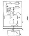
- FIG 1illustrates a prior art system comprising an external charger for charging an implantable pulse generator (IPG), and shows the charge controller and battery protection aspects of the IPG.
- IPGimplantable pulse generator
- Figure 2graphically shows the relationship between battery voltage and battery current during charging of the battery as dictated by the charge controller of Figure 1 .
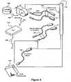
- FIG. 3shows a block diagram that illustrates exemplary implantable, eternal, and surgical components of a spinal cord stimulation (SCS) system that employs an implantable simulator device in accordance with the present invention.
- SCSspinal cord stimulation
- Figure 4shows various components of the SCS system of Figure 1 .
- Figure 5shows a block diagram that illustrates the main components of one embodiment of an implantable stimulator device in which the invention can be used.
- Figure 6shows a block diagram that illustrates another embodiment of an implantable stimulator device in which the invention can be used.
- Figure 7is similar to the system illustrated in Figure 1 , but includes improved battery protection and zero-Volt recovery circuitry in accordance with an embodiment of the invention.
- Figure 8illustrates the various sensors used in conjunction with the improved protection and zero-Volt recovery circuitry of Figure 7 .
- Figure 9illustrates the main switch used in the improved protection and zero-Volt recovery circuitry of Figure 7 , and shows parasitic current paths that can exist.
- the disclosed implantable stimulator devicemay comprise implantable pulse generator (IPG), or similar electrical stimulator and/or electrical sensor, that may be used as a component of numerous different types of stimulation systems. More specifically, the description that follow relates to use of the invention within a spinal cord stimulation (SCS) system as an exemplary embodiment.
- SCSspinal cord stimulation
- the inventionis not so limited. Rather, the invention may be used with any type of implantable electrical circuitry that could benefit from improved battery protection and zero-Volt recovery techniques.
- the present inventionmay be used as part of a pacemaker, an implantable pump, a defibrillator, a cochlear stimulator, a retinal stimulator, a stimulator configured to produce coordinated limb movement, a cortical or deep brain stimulator, or in any other stimulator configured to treat urinary incontinence, sleep apnea, shoulder sublaxation, etc.
- the techniquecan be used in non-medical and/or non-implantable devices or systems as well, i.e., in any device or system in which zero-Volt battery recovery and/or protection is necessary or desirable.
- the implantable components 10include an implantable pulse generator (IPG) 100, an electrode array 110, and (as needed) a lead extension 120.
- IPGimplantable pulse generator
- the extension 120may be used to electrically connect the electrode array 110 to the IPG 100.
- the IPG 100may comprise a rechargeable, multichannel, telemetry-controlled, pulse generator housed in a rounded high-resistivity titanium alloy case to reduce eddy current heating during the inductive charging process.
- the IPG 100may provide electrical stimulation through a multiplicity of electrodes, e.g., sixteen electrodes E 1 through E 16 , included within the electrode array 110.
- the IPG 100may include stimulating electrical circuitry ("stimulating electronics, a power source, e.g., a rechargeable battery, and a telemetry system, the latter of which is particularly relevant to embodiments of the disclosed invention.
- the IPG 100is placed in a surgically-made pocket either in the abdomen, or just at the top of the buttocks. It may, of course, also be implanted in other locations of the patient's body.
- the IPG 100is connected to the lead system, comprising the lead extension 120, if needed, and the electrode array 110.
- the lead extension 120for example, may be tunneled up to the spinal column.
- the lead system 110 and lead extension 120are intended to be permanent.
- the IPG 104may be replaced if it fails.
- the electrode array 110 and its associated lead systemtypically interface with the implantable pulse generator (IPG) 100 via the lead extension system 120 just mentioned.
- the electrode array 110may also be connected to an external trial stimulator 140, through the use of a percutaneous lead extension 132 and/or an external cable 134.
- the external trial stimulator 140typically includes the same or similar pulse generation circuitry as does the IPG 100, and is used on a trial basis, e.g., for 7-10 days, after the electrode array has been implanted and prior to implantation of the IPG 100, to test the effectiveness of the stimulation that is to be provided.
- a hand-held programmer (HHP) 202may be used to control the IPG 100 via a suitable non-invasive communications link 201, e.g., an RF link. Such control allows the IPG 100 to be turned on or off, and generally allows stimulation parameters, e.g., pulse amplitude, width, and rate, to be set by a patient or clinician within prescribed limits.
- the HHP 202may also be linked with the external trial stimulator 140 through another link 205', e.g., an infra red link.
- CPclinician's programmer
- An external charger 208non-invasively coupled with the IPG 100 through link 290, e.g., an inductive link, allows energy stored or otherwise made available to the charger 208 to be coupled into the rechargeable battery 180 housed within the IPG 100, as explained in the Background.
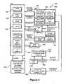
- the IPGincludes a microcontroller ( ⁇ C) 160 connected to memory circuitry 162.
- the ⁇ C 160typically comprises a microprocessor and associated logic circuitry, which in combination with control logic circuits 166, timer logic 168, and an oscillator and clock circuit 164, generate the necessary control and status signals which allow the ⁇ C 160 to control the operation of the IPG in accordance with a selected operating program and stimulation parameters.
- a "microcontroller” as used hereinshould be understood as any integrated device capable of processing signals in the IPG, including traditional microcontrollers, microprocessors, or other signal processors, including those that are application-specific, such as ASIC chips).
- the operating program and stimulation parametersare telemetered to the IPG 100, where they are received via antenna 250 (which may include a coil 170 and/or other antenna components), processed, e.g., via RF-telemetry circuitry 172, and may be stored, e.g., within the memory 162.
- the RF-telemetry circuitry 172demodulates the signal it receives from the HHP 202 or CP 204 to recover the operating program and/or the stimulation parameters. More specifically, signals received by the antenna 250 are passed through the transmit/receive switch 254 to amplifiers and filters 258.
- the received signalsare demodulated (262) using Frequency Shift Keying (FSK) demodulation for example, and the data is then sent to the microcontroller 160 for processing and/or eventual storage.
- FSKFrequency Shift Keying
- the microcontroller 160sends relevant data to transmission drivers 256, where the carrier is modulated by the data and amplified for transmission.
- the transmit/receive switch 254would then be set to communicate with the transmission drivers 256, which in turn drive the data to the antenna 250 to be broadcast.
- the microcontroller 160is further coupled to monitoring circuits 174 via bus 173.
- the monitoring circuits 174monitor the status of various nodes or other points 175 throughout the IPG 100, e.g., power supply voltages, current values, temperature, the impedance of electrodes attached to the various electrodes E 1 ... E N , and the like.
- Informational data sensed through the monitoring circuit 174may be sent to a remote location external to the IPG (e.g., a non-implanted location) through telemetry circuitry 172 via coil 170.
- the operating power for the TPG 100may be derived from a rechargeable power source 180, which may comprise a lithium-ion or lithium-ion polymer battery, for example, as discussed earlier.
- the rechargeable battery 180provides an unregulated voltage to power circuits 182.
- the battery 180is charged by an electromagnetic field created by an external portable charger 208 ( Figs. 1 , 3 ) as already noted.
- charging coil 270When placed near the IPG 100 (e.g., centimeters away), an electromagnetic field emanating from the portable charger 208 induces a current in charging coil 270 (even through a patient's skin). This current is then rectified and regulated to charge the battery 180, as explained in the Background. Further associated with the charging circuitry is charging telemetry circuitry 272, which is used for example by the IPG 100 to report back to the portable charger 208 when the battery is full, and thus when portable charger can be shut off.
- any of the N electrodesmay be assigned to up to k possible groups or "channels.” In one preferred embodiment, k may equal four. Moreover, any of the N electrodes can operate, or be included in, any of the k channels.
- the channelidentifies which electrodes are selected to synchronously source or sink current to create an electric field in the tissue to be stimulated. Amplitudes and polarities of electrodes on a channel may vary, e.g., as controlled by the HHP 202.
- External programming software in the CP 204is typically used to set parameters including electrode polarity, amplitude, pulse rate and pulse width for the electrodes of a given channel, among other possible programmable features.
- the N programmable electrodescan be programmed to have a positive (sourcing current), negative (sinking current), or off (no current) polarity in any of the k channels.
- each of the N electrodescan operate in a bipolar mode or multipolar mode, e.g., where two or more electrode contacts arc grouped to source/sink current at the same time.
- each of the N electrodescan operate in a monopolar mode where, e.g., the electrode contacts associated with a channel are configured as cathodes (negative), and the case electrode (i.e., the IPG case) is configured as an anode (positive).
- the amplitude of the current pulse being sourced or sunk to or from a given electrode contactmay be programmed to one of several discrete current levels, e.g., between 0 to 10 mA in steps of 0.1 mA.
- the pulse width of the current pulsesis preferably adjustable in convenient increments, e.g., from 0 to 1 milliseconds (ms) in increments of 10 microseconds ( ⁇ s).
- the pulse rateis preferably adjustable within acceptable limits, e.g., from 0 to 1000Hz.
- Other programmable featurescan include slow start/end ramping, burst stimulation cycling (on for X time, off for Y time), and open or closed loop sensing modes.
- the stimulation pulses generated by the IPG 100may be charge balanced. This means that the amount of positive charge associated with a given stimulus pulse is offset with an equal and opposite negative charge. Charge balance may be achieved through coupling capacitors C x , which provide a passive capacitor discharge that achieves the desired charge-balanced condition. Alternatively, active biphasic or multi-phasic pulses with positive and negative phases that are balanced may be used to achieve the needed charge balanced condition.
- the IPG 100is able to individually control the currents at the N electrodes.
- DACDigital-to-Analog Current
- the IPG 100may include N feedthroughs to allow electrical contact to be individually made from inside of the hermetically-sealed case with the N electrodes that form part of the lead system outside of the case.
- the IPG 100may be placed in a surgically-made pocket, e.g., in the abdomen or just at the top of the buttocks, and detachably connected to the lead system (comprising optional lead extension 120 and electrode array 110). While the lead system is intended to be permanent, the IPG 100 may be replaced should it fail.
- the telemetry features of the IPG 100allow the status of the IPG to be checked. For example, when the HHP 202 and/or the CP 204 initiate a programming session with the IPG 100, the capacity of the battery is telemetered so that the external programmer can calculate the estimated time to recharge. Any changes made to the current stimulus parameters are confirmed through back-telemetry, thereby assuring that such changes have been correctly received and implemented within the implant system. Moreover, upon interrogation by the external programmer, all programmable settings stored within the implant system 10 may be uploaded to one or more external programmers.
- the IPG 100'includes both analog and digital dies, or integrated circuits (ICs), which may be housed in a single hermetically-sealed rounded case having, for instance, a diameter of about 45mm and a maximum thickness of about 10mm.
- ICsintegrated circuits
- Many of the circuits contained within the IPG 100'are identical or similar to the circuits contained within the IPG 100, shown in Figure 5 .
- the IPG 100'includes a processor dic, or chip, 160', an RF telemetry circuit 172' (typically realized with discrete components), a charger coil 270', a rechargeable battery 180', battery charger and protection circuits 272', 182', memory circuits 162' (SEEPROM) and 163' (SRAM), a digital IC 191', an analog IC 190', and a capacitor array and header connector 192'.
- a processor dic, or chip, 160'an RF telemetry circuit 172' (typically realized with discrete components), a charger coil 270', a rechargeable battery 180', battery charger and protection circuits 272', 182', memory circuits 162' (SEEPROM) and 163' (SRAM), a digital IC 191', an analog IC 190', and a capacitor array and header connector 192'.
- the capacitor array and header connector 192'include sixteen output decoupling capacitors, as well as respective feed-through connectors for connecting one side of each decoupling capacitor through the hermetically-sealed case to a connector to which the electrode array 110, or lead extension 120, may be detachably connected.
- the processor 160'may be realized with an application specific integrated circuit (ASIC), field programmable gate array (FPGA), or the like that comprises a main device for full bi-directional communication and programming.
- the processor 160'may utilize an 8086 core (the 8086 is a commercially-available microprocessor available from, e.g., Intel), or a low power equivalent thereof, SRAM or other memory, two synchronous serial interface circuits, a serial EEPROM interface, and a ROM boot loader 735.
- the processor die 160'may further include an efficient clock oscillator circuit 164', and (as noted earlier) mixer and modulator/demodulator circuitry implementing the QFAST RF telemetry method.
- An analog-to-digital converter (A/D) circuit 734is also resident on the processor 160' to allow monitoring of various system level analog signals, impedances, regulator status and battery voltage.
- the processor 160'further includes the necessary communication links to other individual ASICs utilized within the IPG 100'.
- the processor 160'like all similar processors, operates in accordance with a program that is stored within its memory circuits.
- the analog IC (AIC) 190'may comprise an ASIC that functions as the main integrated circuit that performs several tasks necessary for the functionality of the IPG 100', including providing power regulation, stimulus output, and impedance measurement and monitoring.
- Electronic circuitry 194'performs the impedance measurement and monitoring function.
- the analog IC 190'may also include output current DAC circuitry 186' configured to supply current to a load, such as tissue, for example.
- the output current DAC circuitry 186'may be configured to deliver up to 20mA aggregate and up to 12.7 mA on a single channel in 0.1 mA steps. However, it will be noted that the output current DAC circuitry 186' may be configured to deliver any amount of aggregate current and any amount of current on a single channel, according to one exemplary embodiment.
- Regulators for the IPG 100'supply the processor and the digital sequencer with a voltage.
- Digital interface circuits residing on the analog IC 190'are similarly supplied with a voltage.
- a programmable regulatorsupplies the operating voltage for the output current DAC circuitry 186'.
- the coupling capacitors C X and electrodes E Xmay all be housed within the hermetically sealed case of the IPG 100.
- a feedthrough pinwhich is included as part of the header connector 192', allows electrical connection to be made between each of the coupling capacitors C N and the respective electrodes E 1 , E 2 , E 3 , ... , or E 16 .
- the digital IC (DigIC) 191'functions as the primary interface between the processor 160' and the output current DAC circuitry 186', and its main function is to provide stimulus information to the output current DAC circuitry 186'.
- the DigIC 191'thus controls and changes the stimulus levels and sequences when prompted by the processor 160'.
- the DigIC 191'comprises a digital application specific integrated circuit (digital ASIC).
- FIG. 7Improved battery protection and zero-Volt recovery circuitry 500 is shown in Figure 7 . Because many of the components are similar to components discussed earlier with respect to Figure 1 , they are labeled with the same element numerals, even if differing slightly in function as noted herein. Protection and zero-Volt recovery circuitry 500 is preferably formed on an integrated circuit, but may also comprise discrete components. Moreover, circuitry 500 may be integrated with the charge controller 684 or with other integrated circuits in the IPG 100, the level of integration and/or combination of functions being merely a design choice.
- protection and zero-Volt recovery circuitry 500comprises in a preferred embodiment two distinct charging paths: one (designated by node “Trickle") for trickle changing, and another (designated by node “Plus”) used for normal charging.
- At least one diode 501(a passive device, unlike a transistor which must be actively gated) intervenes between node Trickle and the battery voltage, Vbat. (If more than one diode is used, they would be serially connected, although this is not shown in Figure 7 for simplicity).
- a main switch 503(preferably a P-channel MOS transistor) intervenes between node Plus and Vbat, which is controlled by a main switch control circuit 505, explained in further detail with respect to Figure 8 .
- Load switch 504intervenes between node Plus and the load (designated by node "Vdd"), and is generally similar in function to the load switch of Figure 1 .
- Vddthe load switch of Figure 1 .
- main switch control 505controlling the former
- charge controller 684for example controlling the latter.
- a diode 502intervenes between nodes Plus and Trickle.
- diode 502, like diode 501,may actually comprise a chain of serially-connected diodes, although Figure 7 shows a single diode for simplicity).
- Protection and zero-Volt recovery circuitry 500basically supports and controls two operative modes: a charging mode and discharging mode.
- the discharging modeis implicated when the battery 180 is coupled to the load, e.g., during normal operation, through main switch 503 and load switch 504.
- the circuit 500can sense a short circuit, i.e., from node Plus or Vdd to ground and/or excessive current draw, either of which evidences a problem with the IPG 100.
- the main switch 503is turned off by main switch control circuit 505 to prevent the battery 180 from being drained, and will remain off until the external charger 208 turns it back on, a point discussed in further detail later.
- the charging modecan further be classified into two sub-modes: a trickle charging mode and a normal charging mode, similar to that discussed with respect to Figures 1 and 2 .
- a trickle charging modeWhen the battery 180 voltage, Vbat, is sensed by the charge controller 684 to be less than the 2.5V, the circuit is in trickle charging mode.
- currentItrickle; approximately 10 mA
- node TrickleTo charge the battery up to 2.5V.
- Vbatequals 2.5V
- the charge controller 684switches to the normal charging mode, thus passing a larger current (Inormal; approximately 50 mA) through node Plus to the battery.
- the main switch 503When the battery 180 is finally fully charged, the main switch 503 is turned off to isolate the battery 180 from the charge controller.
- main switch 503is controlled on and off by main switch control circuitry 505, and it is useful at this point to briefly explain how the logic in this circuitry 505 reacts to open and close the main switch 503.
- Figure 8thus show the various sensing circuits used to open and close the switch 503, not shown in Figure 7 for clarity. While relevant to protection, one skilled in the art will realize that these various sensors may also be integrated with the charge controller 684.
- a short circuit sensor 510receives as input either the battery voltage, Vbat, or the voltage at node Plus as shown.
- Reed switch 522preferably a discrete component separate from other integrated circuitry, can be used to freely disable the main switch 503, and thus terminate charging or discharging of the battery 180, for any number of other reasons.
- Short circuit sensor 510monitors the voltage at node Plus. If this voltage falls below an acceptable value (e.g., 0.8V), sensor 510 infers that a short circuit is present between Plus and ground (or between Vdd and ground if load switch 504 is on), and so directs the main switch control circuitry 505 to disable main switch 503, thus isolating the battery 180 to prevent it from draining. For safety reasons, should short circuit sensor 510 direct the main switch control circuitry 505 to disable the main switch 503, it is preferable that the main switch 503 stay permanently open until the external charger 208 ( Fig. 1 ) is used to raise node Plus to an acceptable operating voltage. Of course, whether the external charger 208 will be capable of resetting main switch 503 ultimately depends on removal of the condition or "glitch" which caused the initial short circuit..
- an acceptable valuee.g. 0.8V
- Battery voltage sensor 512senses the voltage of the battery 180, Vbat, and can be used to inform the charge controller 684 of this value, e.g., so that the charge controller knows when to transition between trickle and normal charging. Battery voltage sensor 512 is also useful to assess whether Vbat is too high (e.g., greater than 4.2V), and if so, to activate self discharge circuit 514 to lower the voltage to a proper level. During normal operation, the battery voltage sensor 512 directs the main switch control 505 to close main switch 503 should Vbat be within normal operating parameters, e.g., between 2.5V and 4.2V, and otherwise directs control 505 to disable switch 503. The various voltage levels of interest to the battery voltage sensor 512 (e.g., 2.5V, 4.2V), may be trimmed to adjust their values to account for process variations via a multi-bit bus (not shown).
- a multi-bit busnot shown.
- Excess current sensor 516is used to disconnect the battery 180 under conditions of high current draw.
- the main switch substrate sensor 520monitors the polarity of current flow (charge or discharge) across the main switch 503 and ties the N-well of the main switch 315 to the higher of Plus or Vbat to prevent current loss to the substrate, as described further below.
- the various sensors illustrated in Figure 8may be constructed using standard reference circuits, such as bandgap voltage reference circuits, voltage dividers, differential amplifiers, comparators, etc. Because such sensors circuits are well known and may take several different forms as one skilled in the art will appreciate, they are not discussed further.
- the main switch 503is implemented with a PMOS transistor residing in an N well, such as is shown in cross-section in Figure 9 . It should be noted that the source and drain regions of the main switch 503 (which are otherwise symmetrically fabricated as one skilled in the art will appreciate, and hence arbitrarily named in Figure 9 ) will be subject to different voltages depending on whether the battery 180 is being charged or discharged. For example, during normal charging, node Plus is brought high due to biasing from the charge controller 684; while being discharged, Vbat is brought relatively high by the battery 180.
- the N well potential(node “Bias" in Figure 9 ) is tied to the higher of potential of the source or drain of main switch 503 at all times, rather than simply always having the N well biased to Vbat as would be more typical for a PMOS transistor. This prevents unwanted current draw to the substrate.
- the N well (node Bias)is biased to the higher of the source or drain nodes of main switch 503 via a polarity control circuit, such as the main switch substrate sensor 520 discussed above (see Fig. 8 ).
- a polarity control circuitsuch as the main switch substrate sensor 520 discussed above (see Fig. 8 ).
- the trickle charging pathnode Trickle; current Itrickle
- normal charging pathnode Plus; current Inormal
- Zero-Volt recoveryis the driving factor for separating these two charging paths.
- node Plusis tied to Vbat. This is accomplished in one embodiment through the use of diode(s) 502.
- the function of diode(s) 502is to match the voltage drop across diode(s) 501 during trickle charging to keep the voltage at Plus the same as Vbat so that trickle charge current does not leak to the substrate through switch 503. In other words, if 502 were not present, the voltage at Plus could be below the battery and 503 could leak to the substrate.
- diodes 501 and 502are shown as single diodes in Figure 7 , different numbers of diodes can be used. In a preferred embodiment, two diodes in series are used for diodes 501 and 502. Moreover, it should be realized that diodes 501, 502 can be realized as transistors in which one of the source and drain are tied to the substrate (well), as is well known. As such, "diode” as used herein should be understood as including such structures, and any other structures capable of one-way current transmission.
- trickle chargingcan be accomplished by having the charge controller 684 providing a significantly high bias to node Trickle to overcome the forward threshold on diode 501 to produce the desired trickle current, Itrickle.
- Vbatwill raise to a level at which normal charging can take place, e.g., at 2.5V.
- monitoring of Vbat for this cross-over conditionis the function of battery voltage sensor 512 of Figure 8 , which, like main switch control 505 will start functioning reliably once Vbat is charged to a suitably high level (e.g., 2.0V).
- protection and zero-Volt recovery circuitry 500is capable of both protecting the battery, and charging the battery 180 even from a zero-Volt condition. Protection is present by the ability to isolate the battery 180 from both the load via load switch 504 and from the charge controller via main switch 503 and via diode 501 (which will prevent battery discharge back to the charge controller 684). Such protection does not hamper the circuitry 500 from being charged. Instead, through the provision of two separate charging paths, Plus and Trickle, the battery can be charged through one path (Trickle) without concern that the protection circuitry will inhibit low-level charging when the battery is at low voltages. Once suitable charged, the other path (Plus) is used to charge the battery through the protection circuitry (e.g., main switch 503) to nominal voltages.
- the protection circuitrye.g., main switch 503
- the battery and loadare protectable from adverse voltage and current conditions, and the battery can be fully recovered. As noted earlier, this is especially important when the circuitry 500 is incorporated in an implantable medical device such as an IPG 100, for failure to recover a fully depleted battery might otherwise warrant surgical extraction of the device.
Landscapes
- Engineering & Computer Science (AREA)
- Health & Medical Sciences (AREA)
- Biomedical Technology (AREA)
- Nuclear Medicine, Radiotherapy & Molecular Imaging (AREA)
- Radiology & Medical Imaging (AREA)
- Life Sciences & Earth Sciences (AREA)
- Animal Behavior & Ethology (AREA)
- General Health & Medical Sciences (AREA)
- Public Health (AREA)
- Veterinary Medicine (AREA)
- Computer Networks & Wireless Communication (AREA)
- Power Engineering (AREA)
- Heart & Thoracic Surgery (AREA)
- Chemical & Material Sciences (AREA)
- Chemical Kinetics & Catalysis (AREA)
- Electrochemistry (AREA)
- General Chemical & Material Sciences (AREA)
- Manufacturing & Machinery (AREA)
- Cardiology (AREA)
- Charge And Discharge Circuits For Batteries Or The Like (AREA)
- Electrotherapy Devices (AREA)
- Neurology (AREA)
- Prostheses (AREA)
Abstract
Description
- This international patent application claims priority to
U.S. Provisional Patent Application Serial No. 60/748,240, filed December 7, 2005 - The present invention relates generally to circuitry and techniques for battery protection and zero-Volt battery recovery preferably for use in an implantable medical device such as an implantable stimulator device, or more specifically an implantable pulse generator.
- Implantable stimulation devices generate and deliver electrical stimuli to body nerves and tissues for the therapy of various biological disorders, such as pacemakers to treat cardiac arrhythmia, defibrillators to treat cardiac fibrillation, cochlear stimulators to treat deafness, retinal stimulators to treat blindness, muscle stimulators to produce coordinated limb movement, spinal cord stimulators to treat chronic pain, cortical and deep brain stimulators to treat motor and psychological disorders, and other neural stimulators to treat urinary incontinence, sleep apnea, shoulder sublaxation, etc. The present invention may find applicability in all such applications, although the description that follows will generally focus on the use of the invention within a Spinal Cord Stimulation (SCS) system, such as that disclosed in U.S. Patent
US 2007/0038250 . - Spinal cord stimulation is a well-accepted clinical method for reducing pain in certain populations of patients. An SCS system typically includes an Implantable Pulse Generator (IPG) or Radio-Frequency (RF) transmitter and receiver, electrodes, at least one electrode lead, and, optionally, at least one electrode lead extension. The electrodes, which reside on a distal end of the electrode lead, are typically implanted along the dura of the spinal cord, and the IPG or RF transmitter generates electrical pulses that are delivered through the electrodes to the nerve fibers within the spinal column. Individual electrode contacts (the "electrodes") are arranged in a desired pattern and spacing to create an electrode array. Individual wires within one or more electrode leads connect with cach electrode in the array. The electrode lead(s) exit the spinal column and generally attach to one or more electrode lead extensions. The electrode lead extensions, in turn, are typically tunneled around the torso of the patient to a subcutaneous pocket where the IPG or RF transceiver is implanted. Alternatively, the electrode lead may directly connect with the IPG or RF transceiver. For examples of other SCS systems and other stimulation systems, see
U.S. Patents 3,646,940 and3,822,708 .
Of course, implantable pulse generators are active devices requiring energy for operation, such as is provided by an implanted battery or an external power source. - As should be obvious, an TPG needs electrical power to function. Such power can be provided in several different ways, such as through the use of a rechargeable or non-rechargeable battery or through electromagnetic (EM) induction provided from an external charger, or from combinations of these and other approaches, which are discussed in further detail in
U.S. Patent 6,553,263 ("the '263 patent"). Perhaps the favorite of these approaches is to use a rechargeable battery in the IPG, such as a lithium-ion battery or a lithium-ion polymer battery. Such a rechargeable battery can generally supply sufficient power to run an IPG for a sufficient period (e.g., a day or more) between recharging. Recharging can occur through the use of EM induction, in which EM fields are sent by an external charger to the IPG. Thus, when the battery needs recharging, the patient in which the IPG is implanted can activate the external charger to percutaneously (i.e., through the patient's flesh) charge the battery (e.g., at night when the patient is sleeping or during other convenient periods). - The basics of such a system are shown in
Figure 1 , which is largely descriptive of salient contents of the '263 patent. As shown, the system comprises in relevant part theexternal charger 208 and IPG 100. As noted, acoil 279 in thecharger 208 produces anEM field 290 capable of percutaneous transmission through a patient'sflesh 278. Theexternal charger 208 may be powered by any known means, such as via a battery or by plugging into a wall outlet, for example. TheEM field 290 is met at the IPG 100 by anothercoil 270, and accordingly an AC voltage is induced in thatcoil 270. This AC voltage is turn is rectified to a DC voltage at arectifier 682, which may comprise a standard bridge circuit. (There may additionally be data telemetry associated with theEM field 290, but this detail is ignored as impertinent to the present disclosure). The rectified DC voltage is in turn sent to acharge controller 684, which operates generally to regulate the DC voltage and to produce either a constant voltage or constant current output as necessary for recharging thebattery 180. The output of thecharge controller 684, i.e., how aggressively the charge controller charges thebattery 180, is dependent on the battery voltage, Vbat, as will be explained in further detail later. (Thecharge controller 684 can also be used to report thebattery 180's charge status back to theexternal charge 208 via backtelemetry using coil 270, as disclosed in the '263 application; however, because this function is not particularly relevant to this disclosure, it is not further discussed). - The output of the
charge controller 684 is in turn met by twoswitches battery 180 from over-charging or over-discharging. As shown, these transistors are N-channel transistors, which will be "on," and thus capable of connecting thecharge controller 684's output to thebattery 180 when their gates are biased. Control of these gates is provided by abattery protection circuit 686, which receives the battery current and voltage, That and Vbat, as control signals, again as will be explained in further detail latter. For example, whenever thebattery 180 exhibits too high a voltage, thebattery protection circuit 686 will turn off the gate of the over-chargingtransistor 701 to protect the battery from further charging. A fuse positioned between thetransistors battery 180 may also be used to further protect the battery from very high current events (not shown). Thebattery 180 is coupled to one of several loads in theIPG 100, such as the electrode stimulation circuitry, i.e., the circuits thebattery 180 ultimately powers. Thebattery 180 is coupled to such loads through aload switch 504, which can isolate thebattery 180 from the load to protect one from adverse effects of the other. Thisload switch 504 is preferably part of thecharge controller 684, which may comprise its own integrated circuit, although this is not strictly necessary. - As discussed in the above-referenced '263 patent, the
charging circuitry 684 can charge thebattery 180 in different ways, depending on the status of the battery voltage, Vbat. Without reiterating the contents of that disclosure, such selective charging of thebattery 180 is beneficial for safely charging the battery, particularly when a lithium-ion-based battery is used. Essentially, this safe charging scheme charges thebattery 180 with smaller currents when the battery voltage Vbat is significantly depleted, and charges with higher currents when the battery voltage is still undercharged but at higher, safer levels. - Consider an embodiment in which Vbat = 4.2V represents a nominal voltage for the
battery 180. When Vbat < 2.5V, thecharge controller 684 will "trickle" charge thebattery 180 with a low level current, e.g., Ibat = 10 mA. As the battery charges and as Vbat increases, higher charging current can be used. For example, once Vbat > 2.5V, a charging current of Ibat = 50 mA may be set by thecharge controller 684. Once the nominal voltage of 4.2V is approached, thecharge controller 684 may continue to charge thebattery 180 by providing a constant voltage instead of constant current on its output, which as charging continues is manifest in a gradual decay of the battery current. The relationship between Vbat and That during battery charging is graphically illustrated inFigure 2 . Of course, these various current and voltage values are merely exemplary, and other parameters may be suitable depending on the system at hand. Also, more than two levels of charging current (e.g., 10 mA, 25 mA, and 50 mA) can be used in stair-step fashion. - As noted earlier, the
battery protection circuit 686 prevents the battery from potential damage during charging by disconnecting the battery from thecharge controller 684. Specifically, Vbat exceeds a safe value (e.g., greater than 4.2V), then the over-chargingtransistor 701 is disabled by thebattery protection circuit 686 to block further charging. Likewise, if the battery voltage is less than a predetermined value and if Ibat exceeds a predetermined value, over-dischargetransistor 702 is disabled to prevent discharging of the battery. While disclosed as controlling twotransistors battery protection circuit 686 may control a single disabling protection transistor which functions to disable thebattery 180 during both over-charging and over-discharging.Load switch 504 may be similarly controlled to isolate the components to protect them from adverse voltages and currents. - While the charging and protection circuitry of
Figure 1 is suitable, its functionality may be hampered at extremely low battery voltages. As the '263 patent explains, this is because thebattery protection circuit 686 is powered by the battery voltage, Vbat, and hence when Vbat is extremely low (e.g., approaching zero Volts), thebattery protection circuitry 686 may not function as desired. In this regard, note that when Vbat is extremely low, and thus when thebattery 180 is in need of charging, thebattery protection circuit 686 needs to be able to turntransistors charging controller 684 will not be able to pass a charging current, Ibat, to the battery. However, when Ibat is low, thebattery protection circuit 686 may have difficulty generating a sufficient voltage to turn on the gates of the N-channel transistors battery protection circuitry 686 must be able to produce a gate voltage for the transistors that is greater than Vgs (i.e., the potential difference between the gate and source of the transistors). In short, the battery protection circuitry needs to be able to produce a gate voltage which exceeds a threshold voltage (Vt) of the transistors given the source voltages apparent at the transistors. If Vbat is below this threshold voltage, thebattery protection circuit 686 may not be able to produce a suitably-high gate voltage to turntransistors - Should this occur, the
battery 180 cannot be charged, even though Vbat is low and hence thebattery 180 is very much in need of charging. In other words, the charging and protection circuitry inFigure 1 is potentially susceptible to failure at when Vbat is extremely low, i.e., at zero Volts or near-zero Volts. In a worst case this would mean that the IPG 100 is unrecoverable, and if implanted in a patient, may require the drastic step of surgical removal and replacement of the device. But this is unfortunate, because patients in which IPGs are implanted cannot necessarily be relied upon to diligently charge their implanted devices, and hence the risk of a depleted, unrecoverable battery is very real. - As a result, improved circuitry and techniques for protection and zero-Volt recovery for batteries in implantable medical devices would be beneficial. Such solutions are provided herein.
- A solution to this problem is provided by a circuit and a recharging method according to the independent claims.
- Circuitry useable to protect and reliably charge a rechargeable battery, even from a zero-volt state, is disclosed, and is particularly useful when employed in an implantable medical device. The circuit includes two charging paths, a first path for trickle charging the battery at a relatively low current when the battery voltage is below a threshold, and a second path for charging the battery at relatively higher currents that the battery voltage is above a certain threshold. A passive diode is used in the first trickle-charging path which allows trickle charging even when the battery voltage is too low for reliable gating, while a gateable switch (preferably a PMOS transistor) is used in the second higher-current charging path when the voltage is higher and the switch can therefore be gated more reliably. A second diode between the two paths ensures no leakage to the substrate through the gateable switch during trickle charging. The load couples to the battery through the switch, and preferably through a second switch specifically used for decoupling the load.
- The above and other aspects of the present invention will be more apparent from the following more particular description thereof, presented in conjunction with the following drawings wherein:
Figure 1 illustrates a prior art system comprising an external charger for charging an implantable pulse generator (IPG), and shows the charge controller and battery protection aspects of the IPG.Figure 2 graphically shows the relationship between battery voltage and battery current during charging of the battery as dictated by the charge controller ofFigure 1 .Figure 3 shows a block diagram that illustrates exemplary implantable, eternal, and surgical components of a spinal cord stimulation (SCS) system that employs an implantable simulator device in accordance with the present invention.Figure 4 shows various components of the SCS system ofFigure 1 .Figure 5 shows a block diagram that illustrates the main components of one embodiment of an implantable stimulator device in which the invention can be used.Figure 6 shows a block diagram that illustrates another embodiment of an implantable stimulator device in which the invention can be used.Figure 7 is similar to the system illustrated inFigure 1 , but includes improved battery protection and zero-Volt recovery circuitry in accordance with an embodiment of the invention.Figure 8 illustrates the various sensors used in conjunction with the improved protection and zero-Volt recovery circuitry ofFigure 7 .Figure 9 illustrates the main switch used in the improved protection and zero-Volt recovery circuitry ofFigure 7 , and shows parasitic current paths that can exist.- The following description is of the best mode presently contemplated for carrying out the invention. This description is not to be taken in a limiting sense, but is made merely for the purpose of describing the general principles of the invention. The scope of the invention should be determined with reference to the claims and their equivalents.
- Before discussing the battery protection and zero-Volt recovery aspects of the invention that is the focus of this disclosure, the circuitry, structure, and function of an implantable stimulator device in which the disclosed circuitry and technique can be used is set forth for completeness with respect to
Figures 3-6 . The disclosed implantable stimulator device may comprise implantable pulse generator (IPG), or similar electrical stimulator and/or electrical sensor, that may be used as a component of numerous different types of stimulation systems. More specifically, the description that follow relates to use of the invention within a spinal cord stimulation (SCS) system as an exemplary embodiment. However, it is to be understood that the invention is not so limited. Rather, the invention may be used with any type of implantable electrical circuitry that could benefit from improved battery protection and zero-Volt recovery techniques. For example, the present invention may be used as part of a pacemaker, an implantable pump, a defibrillator, a cochlear stimulator, a retinal stimulator, a stimulator configured to produce coordinated limb movement, a cortical or deep brain stimulator, or in any other stimulator configured to treat urinary incontinence, sleep apnea, shoulder sublaxation, etc. Moreover the technique can be used in non-medical and/or non-implantable devices or systems as well, i.e., in any device or system in which zero-Volt battery recovery and/or protection is necessary or desirable. - Turning first to
Figure 3 , a block diagram is shown that illustrates the various components of an exemplary SCS system in which the invention may be used. These components may be subdivided into three broad categories:implantable components 10,external components 20, andsurgical components 30. As seen inFigure 3 , theimplantable components 10 include an implantable pulse generator (IPG) 100, anelectrode array 110, and (as needed) alead extension 120. Theextension 120 may be used to electrically connect theelectrode array 110 to theIPG 100. In an exemplary embodiment, theIPG 100, described more fully below in connection withFigures 5 or6 , may comprise a rechargeable, multichannel, telemetry-controlled, pulse generator housed in a rounded high-resistivity titanium alloy case to reduce eddy current heating during the inductive charging process. TheIPG 100 may provide electrical stimulation through a multiplicity of electrodes, e.g., sixteen electrodes E1 through E16, included within theelectrode array 110. - In this regard, the
IPG 100 may include stimulating electrical circuitry ("stimulating electronics, a power source, e.g., a rechargeable battery, and a telemetry system, the latter of which is particularly relevant to embodiments of the disclosed invention. Typically, theIPG 100 is placed in a surgically-made pocket either in the abdomen, or just at the top of the buttocks. It may, of course, also be implanted in other locations of the patient's body. Once implanted, theIPG 100 is connected to the lead system, comprising thelead extension 120, if needed, and theelectrode array 110. Thelead extension 120, for example, may be tunneled up to the spinal column. Once implanted and any trial stimulation period is complete, thelead system 110 andlead extension 120 are intended to be permanent. In contrast, the IPG 104 may be replaced if it fails. - As seen best in
Figure 4 , and as also illustrated inFigure 3 , theelectrode array 110 and its associated lead system typically interface with the implantable pulse generator (IPG) 100 via thelead extension system 120 just mentioned. Theelectrode array 110 may also be connected to anexternal trial stimulator 140, through the use of apercutaneous lead extension 132 and/or anexternal cable 134. Theexternal trial stimulator 140 typically includes the same or similar pulse generation circuitry as does theIPG 100, and is used on a trial basis, e.g., for 7-10 days, after the electrode array has been implanted and prior to implantation of theIPG 100, to test the effectiveness of the stimulation that is to be provided. - Still with reference to
Figures 3 and4 , and as noted earlier, a hand-held programmer (HHP) 202 may be used to control theIPG 100 via a suitable non-invasive communications link 201, e.g., an RF link. Such control allows theIPG 100 to be turned on or off, and generally allows stimulation parameters, e.g., pulse amplitude, width, and rate, to be set by a patient or clinician within prescribed limits. TheHHP 202 may also be linked with theexternal trial stimulator 140 through another link 205', e.g., an infra red link. Detailed programming of theIPG 100 is preferably accomplished through the use of an external clinician's programmer (CP) 204 (Fig. 3 ), which may also be hand-held and which may be coupled to theIPG 100 directly vialink 201a or indirectly through theHHP 202. Anexternal charger 208, non-invasively coupled with theIPG 100 throughlink 290, e.g., an inductive link, allows energy stored or otherwise made available to thecharger 208 to be coupled into therechargeable battery 180 housed within theIPG 100, as explained in the Background. - Turning next to
Figure 5 , a block diagram is shown that illustrates the main components of one embodiment of an implantable pulse generator (IPG) 100 in which embodiments of the invention may be used. As seen inFigure 5 , the IPG includes a microcontroller (µC) 160 connected tomemory circuitry 162. TheµC 160 typically comprises a microprocessor and associated logic circuitry, which in combination withcontrol logic circuits 166,timer logic 168, and an oscillator andclock circuit 164, generate the necessary control and status signals which allow theµC 160 to control the operation of the IPG in accordance with a selected operating program and stimulation parameters. (A "microcontroller" as used herein should be understood as any integrated device capable of processing signals in the IPG, including traditional microcontrollers, microprocessors, or other signal processors, including those that are application-specific, such as ASIC chips). - The operating program and stimulation parameters are telemetered to the
IPG 100, where they are received via antenna 250 (which may include acoil 170 and/or other antenna components), processed, e.g., via RF-telemetry circuitry 172, and may be stored, e.g., within thememory 162. As noted earlier, the RF-telemetry circuitry 172 demodulates the signal it receives from theHHP 202 orCP 204 to recover the operating program and/or the stimulation parameters. More specifically, signals received by theantenna 250 are passed through the transmit/receiveswitch 254 to amplifiers and filters 258. From there, the received signals are demodulated (262) using Frequency Shift Keying (FSK) demodulation for example, and the data is then sent to themicrocontroller 160 for processing and/or eventual storage. When RF-telemetry circuitry 172 is used to transmit information to theHHP 202 orCP 204 to report in some fashion on its status, themicrocontroller 160 sends relevant data totransmission drivers 256, where the carrier is modulated by the data and amplified for transmission. The transmit/receiveswitch 254 would then be set to communicate with thetransmission drivers 256, which in turn drive the data to theantenna 250 to be broadcast. - The
microcontroller 160 is further coupled to monitoringcircuits 174 viabus 173. Themonitoring circuits 174 monitor the status of various nodes orother points 175 throughout theIPG 100, e.g., power supply voltages, current values, temperature, the impedance of electrodes attached to the various electrodes E1 ... EN, and the like. Informational data sensed through themonitoring circuit 174 may be sent to a remote location external to the IPG (e.g., a non-implanted location) throughtelemetry circuitry 172 viacoil 170. - The operating power for the
TPG 100 may be derived from arechargeable power source 180, which may comprise a lithium-ion or lithium-ion polymer battery, for example, as discussed earlier. Therechargeable battery 180 provides an unregulated voltage topower circuits 182. Thepower circuits 182, in turn, generate thevarious voltages 184, some of which are regulated and some of which are not, as needed by the various circuits located within theIPG 100. In a preferred embodiment, thebattery 180 is charged by an electromagnetic field created by an external portable charger 208 (Figs. 1 ,3 ) as already noted. When placed near the IPG 100 (e.g., centimeters away), an electromagnetic field emanating from theportable charger 208 induces a current in charging coil 270 (even through a patient's skin). This current is then rectified and regulated to charge thebattery 180, as explained in the Background. Further associated with the charging circuitry is chargingtelemetry circuitry 272, which is used for example by theIPG 100 to report back to theportable charger 208 when the battery is full, and thus when portable charger can be shut off. - In one exemplary embodiment, any of the N electrodes may be assigned to up to k possible groups or "channels." In one preferred embodiment, k may equal four. Moreover, any of the N electrodes can operate, or be included in, any of the k channels. The channel identifies which electrodes are selected to synchronously source or sink current to create an electric field in the tissue to be stimulated. Amplitudes and polarities of electrodes on a channel may vary, e.g., as controlled by the
HHP 202. External programming software in theCP 204 is typically used to set parameters including electrode polarity, amplitude, pulse rate and pulse width for the electrodes of a given channel, among other possible programmable features. - The N programmable electrodes can be programmed to have a positive (sourcing current), negative (sinking current), or off (no current) polarity in any of the k channels. Moreover, each of the N electrodes can operate in a bipolar mode or multipolar mode, e.g., where two or more electrode contacts arc grouped to source/sink current at the same time. Alternatively, each of the N electrodes can operate in a monopolar mode where, e.g., the electrode contacts associated with a channel are configured as cathodes (negative), and the case electrode (i.e., the IPG case) is configured as an anode (positive).
- Further, the amplitude of the current pulse being sourced or sunk to or from a given electrode contact may be programmed to one of several discrete current levels, e.g., between 0 to 10 mA in steps of 0.1 mA. Also, the pulse width of the current pulses is preferably adjustable in convenient increments, e.g., from 0 to 1 milliseconds (ms) in increments of 10 microseconds (µs). Similarly, the pulse rate is preferably adjustable within acceptable limits, e.g., from 0 to 1000Hz. Other programmable features can include slow start/end ramping, burst stimulation cycling (on for X time, off for Y time), and open or closed loop sensing modes.
- The stimulation pulses generated by the
IPG 100 may be charge balanced. This means that the amount of positive charge associated with a given stimulus pulse is offset with an equal and opposite negative charge. Charge balance may be achieved through coupling capacitors Cx, which provide a passive capacitor discharge that achieves the desired charge-balanced condition. Alternatively, active biphasic or multi-phasic pulses with positive and negative phases that are balanced may be used to achieve the needed charge balanced condition. - In short, the
IPG 100 is able to individually control the currents at the N electrodes. Controlling the output current Digital-to-Analog Current (DAC)circuitry 186 using themicrocontroller 160, in combination with thecontrol logic 166 andtimer logic 168, allows each electrode contact to be paired or grouped with other electrode contacts, including the monopolar case electrode, to control the polarity, amplitude, rate, pulse width and channel through which the current stimulus pulses are provided. - As shown in
Figure 5 , much of circuitry included within theTPG 100 may be realized on a single application specific integrated circuit (ASIC) 190. This allows the overall size of theIPG 100 to be quite small, and readily housed within a suitable hermetically-sealed case. TheIPG 100 may include N feedthroughs to allow electrical contact to be individually made from inside of the hermetically-sealed case with the N electrodes that form part of the lead system outside of the case. - As noted earlier, in use, the
IPG 100 may be placed in a surgically-made pocket, e.g., in the abdomen or just at the top of the buttocks, and detachably connected to the lead system (comprisingoptional lead extension 120 and electrode array 110). While the lead system is intended to be permanent, theIPG 100 may be replaced should it fail. - The telemetry features of the
IPG 100 allow the status of the IPG to be checked. For example, when theHHP 202 and/or theCP 204 initiate a programming session with theIPG 100, the capacity of the battery is telemetered so that the external programmer can calculate the estimated time to recharge. Any changes made to the current stimulus parameters are confirmed through back-telemetry, thereby assuring that such changes have been correctly received and implemented within the implant system. Moreover, upon interrogation by the external programmer, all programmable settings stored within theimplant system 10 may be uploaded to one or more external programmers. - Turning next to
Figure 6 , a hybrid block diagram of an alternative embodiment of an IPG 100' that may be used with the invention is illustrated. The IPG 100' includes both analog and digital dies, or integrated circuits (ICs), which may be housed in a single hermetically-sealed rounded case having, for instance, a diameter of about 45mm and a maximum thickness of about 10mm. Many of the circuits contained within the IPG 100' are identical or similar to the circuits contained within theIPG 100, shown inFigure 5 . The IPG 100' includes a processor dic, or chip, 160', an RF telemetry circuit 172' (typically realized with discrete components), a charger coil 270', a rechargeable battery 180', battery charger and protection circuits 272', 182', memory circuits 162' (SEEPROM) and 163' (SRAM), a digital IC 191', an analog IC 190', and a capacitor array and header connector 192'. - The capacitor array and header connector 192' include sixteen output decoupling capacitors, as well as respective feed-through connectors for connecting one side of each decoupling capacitor through the hermetically-sealed case to a connector to which the
electrode array 110, orlead extension 120, may be detachably connected. - The processor 160' may be realized with an application specific integrated circuit (ASIC), field programmable gate array (FPGA), or the like that comprises a main device for full bi-directional communication and programming. The processor 160' may utilize an 8086 core (the 8086 is a commercially-available microprocessor available from, e.g., Intel), or a low power equivalent thereof, SRAM or other memory, two synchronous serial interface circuits, a serial EEPROM interface, and a
ROM boot loader 735. The processor die 160' may further include an efficient clock oscillator circuit 164', and (as noted earlier) mixer and modulator/demodulator circuitry implementing the QFAST RF telemetry method. An analog-to-digital converter (A/D)circuit 734 is also resident on the processor 160' to allow monitoring of various system level analog signals, impedances, regulator status and battery voltage. The processor 160' further includes the necessary communication links to other individual ASICs utilized within the IPG 100'. The processor 160', like all similar processors, operates in accordance with a program that is stored within its memory circuits. - The analog IC (AIC) 190' may comprise an ASIC that functions as the main integrated circuit that performs several tasks necessary for the functionality of the IPG 100', including providing power regulation, stimulus output, and impedance measurement and monitoring. Electronic circuitry 194' performs the impedance measurement and monitoring function.
- The analog IC 190' may also include output current DAC circuitry 186' configured to supply current to a load, such as tissue, for example. The output current DAC circuitry 186' may be configured to deliver up to 20mA aggregate and up to 12.7 mA on a single channel in 0.1 mA steps. However, it will be noted that the output current DAC circuitry 186' may be configured to deliver any amount of aggregate current and any amount of current on a single channel, according to one exemplary embodiment.
- Regulators for the IPG 100' supply the processor and the digital sequencer with a voltage. Digital interface circuits residing on the analog IC 190' are similarly supplied with a voltage. A programmable regulator supplies the operating voltage for the output current DAC circuitry 186'. The coupling capacitors CX and electrodes EX, as well as the remaining circuitry on the analog IC 186', may all be housed within the hermetically sealed case of the
IPG 100. A feedthrough pin, which is included as part of the header connector 192', allows electrical connection to be made between each of the coupling capacitors CN and the respective electrodes E1, E2, E3, ... , or E16. - The digital IC (DigIC) 191' functions as the primary interface between the processor 160' and the output current DAC circuitry 186', and its main function is to provide stimulus information to the output current DAC circuitry 186'. The DigIC 191' thus controls and changes the stimulus levels and sequences when prompted by the processor 160'. In an exemplary embodiment, the DigIC 191' comprises a digital application specific integrated circuit (digital ASIC).
- With the basic structure of an implantable stimulator understood, focus now shifts to a detailed description of the battery protection and zero-Volt recovery aspects that are the focus of this disclosure. It is again worth noting that while particularly useful when implemented in implantable medical devices in which the problem of zero-Volt battery recovery is unique, the disclosed techniques can benefit any device or system in which zero-Volt recovery is beneficial. Thus, disclosure in the context of an implantable medical device should be understood as merely exemplary.
- Improved battery protection and zero-
Volt recovery circuitry 500 is shown inFigure 7 . Because many of the components are similar to components discussed earlier with respect toFigure 1 , they are labeled with the same element numerals, even if differing slightly in function as noted herein. Protection and zero-Volt recovery circuitry 500 is preferably formed on an integrated circuit, but may also comprise discrete components. Moreover,circuitry 500 may be integrated with thecharge controller 684 or with other integrated circuits in theIPG 100, the level of integration and/or combination of functions being merely a design choice. - Briefly, protection and zero-
Volt recovery circuitry 500 comprises in a preferred embodiment two distinct charging paths: one (designated by node "Trickle") for trickle changing, and another (designated by node "Plus") used for normal charging. At least one diode 501 (a passive device, unlike a transistor which must be actively gated) intervenes between node Trickle and the battery voltage, Vbat. (If more than one diode is used, they would be serially connected, although this is not shown inFigure 7 for simplicity). A main switch 503 (preferably a P-channel MOS transistor) intervenes between node Plus and Vbat, which is controlled by a mainswitch control circuit 505, explained in further detail with respect toFigure 8 .Load switch 504 intervenes between node Plus and the load (designated by node "Vdd"), and is generally similar in function to the load switch ofFigure 1 . However, it should be noted that coupling thebattery 180 to the load requires that bothswitches main switch control 505 controlling the former, and thecharge controller 684 for example controlling the latter. Additionally, adiode 502 intervenes between nodes Plus and Trickle. (In other embodiments,diode 502, like diode 501, may actually comprise a chain of serially-connected diodes, althoughFigure 7 shows a single diode for simplicity). - Protection and zero-
Volt recovery circuitry 500 basically supports and controls two operative modes: a charging mode and discharging mode. - The discharging mode is implicated when the
battery 180 is coupled to the load, e.g., during normal operation, throughmain switch 503 andload switch 504. In discharge mode, thecircuit 500 can sense a short circuit, i.e., from node Plus or Vdd to ground and/or excessive current draw, either of which evidences a problem with theIPG 100. When either condition is detected, themain switch 503 is turned off by mainswitch control circuit 505 to prevent thebattery 180 from being drained, and will remain off until theexternal charger 208 turns it back on, a point discussed in further detail later. - The charging mode can further be classified into two sub-modes: a trickle charging mode and a normal charging mode, similar to that discussed with respect to
Figures 1 and 2 . When thebattery 180 voltage, Vbat, is sensed by thecharge controller 684 to be less than the 2.5V, the circuit is in trickle charging mode. As will be seen, during trickle charging, current (Itrickle; approximately 10 mA) is passed from thecharge controller 684 through node Trickle to charge the battery up to 2.5V. Once Vbat equals 2.5V, thecharge controller 684 switches to the normal charging mode, thus passing a larger current (Inormal; approximately 50 mA) through node Plus to the battery. When thebattery 180 is finally fully charged, themain switch 503 is turned off to isolate thebattery 180 from the charge controller. - As noted, the
main switch 503 is controlled on and off by mainswitch control circuitry 505, and it is useful at this point to briefly explain how the logic in thiscircuitry 505 reacts to open and close themain switch 503.Figure 8 thus show the various sensing circuits used to open and close theswitch 503, not shown inFigure 7 for clarity. While relevant to protection, one skilled in the art will realize that these various sensors may also be integrated with thecharge controller 684. - Shown in
Figure 8 are four sensors: a short circuit sensor 510, abattery voltage sensor 512, an excesscurrent sensor 516, and a main switch substrate sensor 520. Each sensor receives as input either the battery voltage, Vbat, or the voltage at node Plus as shown.Reed switch 522, preferably a discrete component separate from other integrated circuitry, can be used to freely disable themain switch 503, and thus terminate charging or discharging of thebattery 180, for any number of other reasons. - Short circuit sensor 510 monitors the voltage at node Plus. If this voltage falls below an acceptable value (e.g., 0.8V), sensor 510 infers that a short circuit is present between Plus and ground (or between Vdd and ground if
load switch 504 is on), and so directs the mainswitch control circuitry 505 to disablemain switch 503, thus isolating thebattery 180 to prevent it from draining. For safety reasons, should short circuit sensor 510 direct the mainswitch control circuitry 505 to disable themain switch 503, it is preferable that themain switch 503 stay permanently open until the external charger 208 (Fig. 1 ) is used to raise node Plus to an acceptable operating voltage. Of course, whether theexternal charger 208 will be capable of resettingmain switch 503 ultimately depends on removal of the condition or "glitch" which caused the initial short circuit.. Battery voltage sensor 512 senses the voltage of thebattery 180, Vbat, and can be used to inform thecharge controller 684 of this value, e.g., so that the charge controller knows when to transition between trickle and normal charging.Battery voltage sensor 512 is also useful to assess whether Vbat is too high (e.g., greater than 4.2V), and if so, to activateself discharge circuit 514 to lower the voltage to a proper level. During normal operation, thebattery voltage sensor 512 directs themain switch control 505 to closemain switch 503 should Vbat be within normal operating parameters, e.g., between 2.5V and 4.2V, and otherwise directscontrol 505 to disableswitch 503. The various voltage levels of interest to the battery voltage sensor 512 (e.g., 2.5V, 4.2V), may be trimmed to adjust their values to account for process variations via a multi-bit bus (not shown).- Excess
current sensor 516, like short circuit sensor 510, is used to disconnect thebattery 180 under conditions of high current draw. In a preferred embodiment,sensor 516 senses excessive current by measuring the voltage drop across themain switch 503, i.e., from node Plus to Vbat. Knowing the "on" resistance of the main switch 503 (preferably between 0.12 to 0.19 ohms when Vbat=3.6V), should the voltage drop suggest an excessive high current draw (e.g., greater than 400 mA), the short circuit sensor 510 directs themain switch control 505 to disable themain switch 503. - The main switch substrate sensor 520 monitors the polarity of current flow (charge or discharge) across the
main switch 503 and ties the N-well of the main switch 315 to the higher of Plus or Vbat to prevent current loss to the substrate, as described further below. - The various sensors illustrated in
Figure 8 may be constructed using standard reference circuits, such as bandgap voltage reference circuits, voltage dividers, differential amplifiers, comparators, etc. Because such sensors circuits are well known and may take several different forms as one skilled in the art will appreciate, they are not discussed further. - The
main switch 503 is implemented with a PMOS transistor residing in an N well, such as is shown in cross-section inFigure 9 . It should be noted that the source and drain regions of the main switch 503 (which are otherwise symmetrically fabricated as one skilled in the art will appreciate, and hence arbitrarily named inFigure 9 ) will be subject to different voltages depending on whether thebattery 180 is being charged or discharged. For example, during normal charging, node Plus is brought high due to biasing from thecharge controller 684; while being discharged, Vbat is brought relatively high by thebattery 180. - Since the source and drain regions of the
main switch 503 arc subject to these different voltage polarities, the N well potential (node "Bias" inFigure 9 ) is tied to the higher of potential of the source or drain ofmain switch 503 at all times, rather than simply always having the N well biased to Vbat as would be more typical for a PMOS transistor. This prevents unwanted current draw to the substrate. - To illustrate this problem, consider normal charging of battery. When charging commences, the provision of current (i.e., voltage) at node Plus may be relatively high when compared with Vbat, i.e., depending on Vbat's current level of charge. If Vbat is coupled to the N well at node Bias, a parasitic PNP bipolar transistor (540;
Fig. 9 ) could turn on, with the result that current meant to trickle charge thebattery 180 would be routed to the substrate of themain switch 503. Such inadvertent siphoning of the current would at least slow the charging of thebattery 180, or if significant, could prevent charging of thebattery 180 altogether. However, this problem is not simply fixed by tying the N well (Bias) to node Plus, because during discharging, the parasitic effect could be realized at the other of the source/drain of the switch 503: that is, during discharge, Vbat could be higher than Plus, which could turn on the parasitic PNP bipolar transistor at the other terminal (542;Fig. 9 ), causing current otherwise useable by the load to be inadvertently drained to the substrate. To address this problem, as noted, the N well (node Bias) is biased to the higher of the source or drain nodes ofmain switch 503 via a polarity control circuit, such as the main switch substrate sensor 520 discussed above (seeFig. 8 ). The design of such a polarity control circuit is easily made by those of skill in the art and can be made in many different ways. - With this overview of the protection and zero-
Volt recovery circuitry 500 in hand, attention can know be focused on how thecircuit 500 operates to protect and charge thebattery 180, even from a completely zero-Volt state. - In this regard, and as noted earlier, note from
Figure 7 that the trickle charging path (node Trickle; current Itrickle) is separated from normal charging path (node Plus; current Inormal). Zero-Volt recovery is the driving factor for separating these two charging paths. By separating the Trickle and Plus nodes, the trickle charging current (Itrickle) can be prevented from flowing into the Plus node, and hence bipolar transistor parasitics in themain switch 503 are not implicated. At the same time, because the trickle current bypasses themain switch 503, potential uncertainty in the status of the switch at low voltages is of little concern. - However, what is of concern is the possibility of current leakage through node Plus to the substrate. This is alleviated in one embodiment by holding node Plus at a suitable voltage level during trickle charging. Specifically, in a preferred embodiment, during trickle charging, node Plus is tied to Vbat. This is accomplished in one embodiment through the use of diode(s) 502. The function of diode(s) 502 is to match the voltage drop across diode(s) 501 during trickle charging to keep the voltage at Plus the same as Vbat so that trickle charge current does not leak to the substrate through
switch 503. In other words, if 502 were not present, the voltage at Plus could be below the battery and 503 could leak to the substrate. - Although
diodes 501 and 502 are shown as single diodes inFigure 7 , different numbers of diodes can be used. In a preferred embodiment, two diodes in series are used fordiodes 501 and 502. Moreover, it should be realized thatdiodes 501, 502 can be realized as transistors in which one of the source and drain are tied to the substrate (well), as is well known. As such, "diode" as used herein should be understood as including such structures, and any other structures capable of one-way current transmission. - With Plus held to Vbat during trickle charging, even if the N well is likewise biased to Vbat, the parasitic bipolar transistor 540 (
Fig. 9 ) cannot turn on due the zero-Volt potential difference between the Plus and the well. Moreover, pursuant to this biasing scheme, all junction nodes of themain switch 503 are held to the same potential, i.e., source = drain = N well = Vbat. The result is that no current can flow throughmain switch 503, regardless of whatever potential is present on the gate of the transistor. That being said, when it is desired for themain switch 503 to be off, it may still be preferable to bias the gate ofmain switch 503 to the higher of the two voltages apparent at its source and drain regions, just as the N well is biased as explained earlier. (Similar circuitry could be used for both of these functions). This even further helps to ensure that the PMOSmain switch 503 will not conduct during trickle charging. - Thus, in contrast to the circuit of
Figure 1 as discussed in the Background, low values for Vbat, which affected the ability to turn ontransistors Fig. 8 ), cannot operate reliably at lower values of Vbat, because trickle charging can reliability occur regardless of what such sensors would otherwise indicate to themain switch control 505, and how themain switch control 505 would bias the gate of themain switch 503. With the Plus node effectively prevented from drawing current during trickle charging, trickle charging can be accomplished by having thecharge controller 684 providing a significantly high bias to node Trickle to overcome the forward threshold on diode 501 to produce the desired trickle current, Itrickle. - Once the
battery 180 has been trickled charged as just described, eventually Vbat will raise to a level at which normal charging can take place, e.g., at 2.5V. By way of review, monitoring of Vbat for this cross-over condition is the function ofbattery voltage sensor 512 ofFigure 8 , which, likemain switch control 505 will start functioning reliably once Vbat is charged to a suitably high level (e.g., 2.0V). Thus, whereas during trickle charging the gate voltage ofmain switch 503 was irrelevant because the voltage conditions in the source, drain, and well prevented current flow, during normal charging, voltages have been charged to a suitable level that themain switch control 505 and other sensors reporting to it can now reliably turn on theswitch 503 to permit the flow of current (Inormal) from thecharge controller 684 to node Plus, and ultimately to thebattery 180. Because the voltage at node Plus will be relatively high during normal charging,diode 502 will be reversed-biased, thus preventing the flow of current to node Trickle. - In summary, protection and zero-
Volt recovery circuitry 500 is capable of both protecting the battery, and charging thebattery 180 even from a zero-Volt condition. Protection is present by the ability to isolate thebattery 180 from both the load viaload switch 504 and from the charge controller viamain switch 503 and via diode 501 (which will prevent battery discharge back to the charge controller 684). Such protection does not hamper thecircuitry 500 from being charged. Instead, through the provision of two separate charging paths, Plus and Trickle, the battery can be charged through one path (Trickle) without concern that the protection circuitry will inhibit low-level charging when the battery is at low voltages. Once suitable charged, the other path (Plus) is used to charge the battery through the protection circuitry (e.g., main switch 503) to nominal voltages. Thus, the battery and load are protectable from adverse voltage and current conditions, and the battery can be fully recovered. As noted earlier, this is especially important when thecircuitry 500 is incorporated in an implantable medical device such as anIPG 100, for failure to recover a fully depleted battery might otherwise warrant surgical extraction of the device. - While the invention herein disclosed has been described by means of specific embodiments and applications thereof, numerous modifications and variations could be made thereto by those skilled in the art without departing from the literal and equivalent scope of the invention set forth in the claims.
Claims (13)
- A protection and recovery circuit (500) for an implantable medical device, comprising:a rechargeable battery (180);a charge controller (684) for charging the rechargeable battery (180).a first charging path between the charge controller (684) and a terminal of the battery (180) for charging the battery through at least one diode (501), wherein the first charging path is active to charge the battery from zero volts when a voltage of the battery is below a threshold; anda second charging path between the charge controller (684) and the terminal of the battery (180) for charging the battery through a gateable first switch (503), wherein the second charging path is active to charge the batter (180) when a voltage of the battery is above the threshold.
- The circuit of claim 1, wherein the gateable first switch (503) is off to deactivate the second charging path.
- The circuit of claim 1, wherein a load is coupled to the second charging path such that the gateable switch (503) is active to couple the battery (180) to the load.
- The circuit of claim 3, further comprising a second switch (504) between the gateable first switch (503) and the load for decoupling the load.
- The circuit of claim 1, further comprising at least one diode (502) between the first charging path and the second charging path.
- The circuit of claim 1, wherein the gateable first switch (503) comprises a PMOS transistor.
- The circuit of claim 6, wherein a well of the PMOS transistor is biased to
a higher of a source or a drain of the PMOS transistor or is biased to the battery voltage or is biased to a voltage output by the charge controller (684) on the first charging path. - A method for recharging a battery in an implantable medical device, comprising:producing a relatively low current to charge a terminal of the battery through a first path when the battery voltage is greater than or equal to zero and less than or equal to a threshold; andproducing a relatively high current to charge the terminal of the battery through a second path when the battery voltage is greater than the threshold, wherein the second path comprises an active gateable component.
- The method of claim 8, wherein the second path is opened by a switch when the battery terminal is being charged through the first path.
- The method of claim 8, wherein the first path comprises only a passive component.
- The method of claim 8, wherein the active gateable component comprises a PMOS transistor whose well is biased to ensure no current leakage through the well.
- The method of claim 8, wherein the active gateable component is deactivated when excessive discharge is detected.
- The method of claim 8, wherein the battery is a lithium-ion battery or a lithium-ion polymer battery.
Priority Applications (1)
| Application Number | Priority Date | Filing Date | Title |
|---|---|---|---|
| EP09004190.6AEP2072080B1 (en) | 2005-12-07 | 2006-10-19 | Battery protection and zero-volt battery recovery system for an implantable medical device |
Applications Claiming Priority (2)
| Application Number | Priority Date | Filing Date | Title |
|---|---|---|---|
| US74824005P | 2005-12-07 | 2005-12-07 | |
| PCT/US2006/060081WO2007067825A1 (en) | 2005-12-07 | 2006-10-19 | Battery protection and zero-volt battery recovery system for an implantable medical device |
Related Child Applications (2)
| Application Number | Title | Priority Date | Filing Date |
|---|---|---|---|
| EP09004190.6ADivisionEP2072080B1 (en) | 2005-12-07 | 2006-10-19 | Battery protection and zero-volt battery recovery system for an implantable medical device |
| EP09004190.6Division-Into | 2009-03-24 |
Publications (2)
| Publication Number | Publication Date |
|---|---|
| EP1960048A1 EP1960048A1 (en) | 2008-08-27 |
| EP1960048B1true EP1960048B1 (en) | 2010-08-04 |
Family
ID=37809684
Family Applications (2)
| Application Number | Title | Priority Date | Filing Date |
|---|---|---|---|
| EP06839472AActiveEP1960048B1 (en) | 2005-12-07 | 2006-10-19 | Battery protection and zero-volt battery recovery system for an implantable medical device |
| EP09004190.6ANot-in-forceEP2072080B1 (en) | 2005-12-07 | 2006-10-19 | Battery protection and zero-volt battery recovery system for an implantable medical device |
Family Applications After (1)
| Application Number | Title | Priority Date | Filing Date |
|---|---|---|---|
| EP09004190.6ANot-in-forceEP2072080B1 (en) | 2005-12-07 | 2006-10-19 | Battery protection and zero-volt battery recovery system for an implantable medical device |
Country Status (8)
| Country | Link |
|---|---|
| US (4) | US7962222B2 (en) |
| EP (2) | EP1960048B1 (en) |
| JP (1) | JP4940244B2 (en) |
| AT (1) | ATE476224T1 (en) |
| CA (1) | CA2632755C (en) |
| DE (1) | DE602006016003D1 (en) |
| ES (1) | ES2349480T3 (en) |
| WO (1) | WO2007067825A1 (en) |
Cited By (1)
| Publication number | Priority date | Publication date | Assignee | Title |
|---|---|---|---|---|
| WO2025172337A1 (en)* | 2024-02-16 | 2025-08-21 | Implantica Patent Ltd | Implantable medical device having a safety unit |
Families Citing this family (86)
| Publication number | Priority date | Publication date | Assignee | Title |
|---|---|---|---|---|
| ES2426255T3 (en) | 2002-06-28 | 2013-10-22 | Boston Scientific Neuromodulation Corporation | Microstimulator that has a built-in power source and a two-way telemetry system |
| US7822480B2 (en) | 2002-06-28 | 2010-10-26 | Boston Scientific Neuromodulation Corporation | Systems and methods for communicating with an implantable stimulator |
| WO2007098200A2 (en) | 2006-02-16 | 2007-08-30 | Imthera Medical, Inc. | An rfid-based apparatus, system, and method for therapeutic treatment of obstructive sleep apnea |
| US9238140B2 (en)* | 2006-08-25 | 2016-01-19 | Cochlear Limited | Current leakage detection |
| US9162068B2 (en) | 2007-07-16 | 2015-10-20 | Boston Scientific Neuromodulation Corporation | Energy efficient resonant driving circuit for magnetically coupled telemetry |
| JP2011505964A (en)* | 2007-12-12 | 2011-03-03 | カーディアック ペースメイカーズ, インコーポレイテッド | Implantable medical device with Hall sensor |
| EP2349139B1 (en) | 2008-10-09 | 2017-05-31 | Imthera Medical, Inc. | Stimulation of a hypoglossal nerve for controlling the position of a patient's tongue |
| US20100274319A1 (en)* | 2009-04-28 | 2010-10-28 | Cochlear Limited | Current leakage detection for a medical implant |
| WO2011036702A1 (en)* | 2009-09-24 | 2011-03-31 | 株式会社 東芝 | Wireless power transmission system |
| WO2011059531A1 (en) | 2009-11-10 | 2011-05-19 | Imthera Medical, Inc. | System for stimulating a hypoglossal nerve for controlling the position of a patient's tongue |
| US8274395B1 (en)* | 2010-02-08 | 2012-09-25 | Adtran, Inc. | Battery monitoring systems and methods |
| ES2371820B1 (en)* | 2010-02-10 | 2013-01-30 | Pneuma Research, S.L. | PROGRAMMABLE PORTABLE DIGITAL TRANSDUCER DEVICE WITH HIGH DISCRIMINATION IN LOW FREQUENCY AND LOW INTENSITY. |
| US20110276110A1 (en)* | 2010-05-07 | 2011-11-10 | Boston Scientific Neuromodulation Corporation | Power Circuitry for an Implantable Medical Device Using a DC-DC Converter |
| EP2575922B1 (en) | 2010-06-07 | 2019-05-22 | Tc1 Llc | Bi-ventricular percutaneous cable |
| WO2011156768A2 (en) | 2010-06-11 | 2011-12-15 | Mojo Mobility, Inc. | System for wireless power transfer that supports interoperability, and multi-pole magnets for use therewith |
| US9044616B2 (en)* | 2010-07-01 | 2015-06-02 | Boston Scientific Neuromodulation Corporation | Charging system for an implantable medical device employing magnetic and electric fields |
| EP2627404B1 (en) | 2010-10-13 | 2017-12-13 | Boston Scientific Neuromodulation Corporation | Architectures for an implantable medical device system having daisy-chained electrode-drive integrated circuits |
| US9393433B2 (en)* | 2011-07-20 | 2016-07-19 | Boston Scientific Neuromodulation Corporation | Battery management for an implantable medical device |
| US8588911B2 (en) | 2011-09-21 | 2013-11-19 | Cochlear Limited | Medical implant with current leakage circuitry |
| US8666504B2 (en)* | 2011-10-24 | 2014-03-04 | Boston Scientific Neuromodulation Corporation | Communication and charging circuitry for a single-coil implantable medical device |
| EP2773423B1 (en) | 2011-11-04 | 2024-01-10 | Nevro Corporation | Medical device communication and charding assemblies for use with implantable signal generators |
| JP6060515B2 (en)* | 2011-12-22 | 2017-01-18 | ソニー株式会社 | Electronic equipment and power supply system |
| US10291067B2 (en) | 2012-07-27 | 2019-05-14 | Tc1 Llc | Computer modeling for resonant power transfer systems |
| US10383990B2 (en) | 2012-07-27 | 2019-08-20 | Tc1 Llc | Variable capacitor for resonant power transfer systems |
| WO2014018974A1 (en) | 2012-07-27 | 2014-01-30 | Thoratec Corporation | Magnetic power transmission utilizing phased transmitter coil arrays and phased receiver coil arrays |
| EP4257174A3 (en) | 2012-07-27 | 2023-12-27 | Tc1 Llc | Thermal management for implantable wireless power transfer systems |
| US9287040B2 (en) | 2012-07-27 | 2016-03-15 | Thoratec Corporation | Self-tuning resonant power transfer systems |
| WO2014018973A1 (en) | 2012-07-27 | 2014-01-30 | Thoratec Corporation | Resonant power transmission coils and systems |
| WO2014018971A1 (en) | 2012-07-27 | 2014-01-30 | Thoratec Corporation | Resonant power transfer systems with protective algorithm |
| WO2014018969A2 (en) | 2012-07-27 | 2014-01-30 | Thoratec Corporation | Resonant power transfer system and method of estimating system state |
| JP6104539B2 (en)* | 2012-09-06 | 2017-03-29 | 日立マクセル株式会社 | Contactless charging system |
| US9142989B2 (en) | 2012-09-07 | 2015-09-22 | Greatbatch Ltd. | Method of minimizing interruptions to implantable medical device recharging |
| US9225190B2 (en) | 2012-09-07 | 2015-12-29 | Manufacturers And Traders Trust Company | Implant current controlled battery charging based on temperature |
| US9209634B2 (en) | 2012-09-07 | 2015-12-08 | Greatbatch Ltd. | Method of improving battery recharge efficiency by statistical analysis |
| US9577446B2 (en)* | 2012-12-13 | 2017-02-21 | Semiconductor Energy Laboratory Co., Ltd. | Power storage system and power storage device storing data for the identifying power storage device |
| WO2014145664A1 (en) | 2013-03-15 | 2014-09-18 | Thoratec Corporation | Integrated implantable tets housing including fins and coil loops |
| EP2984731B8 (en) | 2013-03-15 | 2019-06-26 | Tc1 Llc | Malleable tets coil with improved anatomical fit |
| WO2015023359A1 (en)* | 2013-08-14 | 2015-02-19 | Boston Scientific Neuromodulation Corporation | Power architecture for an implantable medical device having a non-rechargeable battery |
| US10695476B2 (en) | 2013-11-11 | 2020-06-30 | Tc1 Llc | Resonant power transfer systems with communications |
| EP3069358B1 (en) | 2013-11-11 | 2019-06-12 | Tc1 Llc | Hinged resonant power transfer coil |
| EP3072210B1 (en) | 2013-11-11 | 2023-12-20 | Tc1 Llc | Resonant power transfer systems with communications |
| US10004911B2 (en)* | 2014-01-16 | 2018-06-26 | Boston Scientific Neuromodulation Corporation | Circuitry for charging a depleted battery in an implantable medical device without passive trickle charging |
| US9446244B2 (en) | 2014-01-16 | 2016-09-20 | Boston Scientific Neuromodulation Corporation | Determining and forecasting end of life for an implantable medical device having a rechargeable battery |
| US9707395B2 (en) | 2014-01-16 | 2017-07-18 | Boston Scientific Neuromodulation Corporation | Circuitry for charging a battery in an implantable medical device in accordance with historical parameters impacting battery capacity |
| US9707402B2 (en) | 2014-02-14 | 2017-07-18 | Boston Scientific Neuromodulation Corporation | Plug-in accessory for configuring a mobile device into an external controller for an implantable medical device |
| US9345883B2 (en) | 2014-02-14 | 2016-05-24 | Boston Scientific Neuromodulation Corporation | Rechargeable-battery implantable medical device having a primary battery active during a rechargeable-battery undervoltage condition |
| WO2015134871A1 (en) | 2014-03-06 | 2015-09-11 | Thoratec Corporation | Electrical connectors for implantable devices |
| WO2015179177A1 (en) | 2014-05-20 | 2015-11-26 | Nevro Corporation | Implanted pulse generators with reduced power consumption via signal strength/duration characteristics, and associated systems and methods |
| US9533162B2 (en) | 2014-08-21 | 2017-01-03 | Boston Scientific Neuromodulation Corporation | Use of a dedicated remote control as an intermediary device to communicate with an implantable medical device |
| EP3826104B1 (en) | 2014-09-22 | 2023-05-03 | Tc1 Llc | Antenna designs for communication between a wirelessly powered implant to an external device outside the body |
| US20160087480A1 (en)* | 2014-09-23 | 2016-03-24 | Qualcomm Incorporated | Charging Apparatus Including Remote Device Reset |
| US10211649B2 (en)* | 2014-09-25 | 2019-02-19 | Epic Semiconductors Inc | System for generating power and capacitively charging and monitoring a battery pack |
| WO2016057525A1 (en) | 2014-10-06 | 2016-04-14 | Thoratec Corporation | Multiaxial connector for implantable devices |
| EP3191176B1 (en) | 2014-10-22 | 2024-04-10 | Nevro Corp. | Systems and methods for extending the life of an implanted pulse generator battery |
| US10148126B2 (en) | 2015-08-31 | 2018-12-04 | Tc1 Llc | Wireless energy transfer system and wearables |
| WO2017049459A1 (en)* | 2015-09-22 | 2017-03-30 | 广东欧珀移动通信有限公司 | Method and device for controlling charging and electronic device |
| CN106560975B (en)* | 2015-10-02 | 2021-06-01 | 松下知识产权经营株式会社 | Power receiving device and wireless power transmission system |
| WO2017062552A1 (en) | 2015-10-07 | 2017-04-13 | Tc1 Llc | Resonant power transfer systems having efficiency optimization based on receiver impedance |
| EP3493877B1 (en) | 2016-08-05 | 2020-05-13 | Cardiac Pacemakers, Inc. | Active medical device using the internal thoracic vasculature |
| JP6828296B2 (en)* | 2016-08-09 | 2021-02-10 | 株式会社Gsユアサ | Power storage device and charge control method for power storage device |
| EP4084271A1 (en) | 2016-09-21 | 2022-11-02 | Tc1 Llc | Systems and methods for locating implanted wireless power transmission devices |
| US10537731B2 (en) | 2016-11-17 | 2020-01-21 | Cardiac Pacemakers, Inc. | Transvenous mediastinum access for the placement of cardiac pacing and defibrillation electrodes |
| WO2018118818A1 (en) | 2016-12-21 | 2018-06-28 | Cardiac Pacemakers, Inc. | Lead with integrated electrodes |
| US10850067B2 (en) | 2016-12-21 | 2020-12-01 | Cardiac Pacemakers, Inc. | Implantation of an active medical device using the intercostal vein |
| US10675476B2 (en) | 2016-12-22 | 2020-06-09 | Cardiac Pacemakers, Inc. | Internal thoracic vein placement of a transmitter electrode for leadless stimulation of the heart |
| US10751543B2 (en) | 2016-12-22 | 2020-08-25 | Cardiac Pacemakers, Inc. | Azygos, internal thoracic, and/or intercostal vein implantation and use of medical devices |
| US10980570B2 (en) | 2017-01-12 | 2021-04-20 | Cardiac Pacemakers, Inc. | Implantation of an active medical device using the internal thoracic vasculature |
| WO2018136592A2 (en) | 2017-01-18 | 2018-07-26 | Tc1 Llc | Systems and methods for transcutaneous power transfer using microneedles |
| US11077299B2 (en) | 2017-03-07 | 2021-08-03 | Cardiac Pacemakers, Inc. | Implantation of an active medical device |
| US10806932B2 (en) | 2017-03-20 | 2020-10-20 | Cardiac Pacemakers, Inc. | Implantable medical device |
| WO2018187161A1 (en)* | 2017-04-03 | 2018-10-11 | Cardiac Pacemakers, Inc. | Implantable device with rechargeable battery and recharge intelligence |
| WO2018184285A1 (en) | 2017-04-07 | 2018-10-11 | 广东欧珀移动通信有限公司 | Wireless charging system, apparatus, method, and device to be charged |
| EP3462564A4 (en)* | 2017-04-07 | 2019-05-08 | Guangdong Oppo Mobile Telecommunications Corp., Ltd. | SYSTEM, APPARATUS AND METHOD FOR WIRELESS LOADING, AND DEVICE FOR CHARGING |
| KR102268987B1 (en) | 2017-04-07 | 2021-06-24 | 광동 오포 모바일 텔레커뮤니케이션즈 코포레이션 리미티드 | Wireless charging device, wireless charging method and charging standby equipment |
| WO2018195071A1 (en) | 2017-04-18 | 2018-10-25 | Cardiac Pacemakers, Inc. | Active medical device with attachment features |
| EP3401150B1 (en)* | 2017-05-04 | 2022-04-06 | Volvo Car Corporation | Dual voltage unit for a vehicle |
| EP3398818B1 (en) | 2017-05-04 | 2022-07-06 | Volvo Car Corporation | Voltage supply unit, battery balancing method |
| US11020075B2 (en) | 2017-05-12 | 2021-06-01 | Cardiac Pacemakers, Inc. | Implantation of an active medical device using the internal thoracic vasculature |
| CN111406355B (en)* | 2017-12-04 | 2025-07-04 | 株式会社杰士汤浅国际 | Charging control device, power storage device, and charging method |
| WO2019135890A1 (en) | 2018-01-04 | 2019-07-11 | Tc1 Llc | Systems and methods for elastic wireless power transmission devices |
| WO2019152553A1 (en) | 2018-01-30 | 2019-08-08 | Jon Parker | Efficient use of an implantable pulse generator battery, and associated systems and methods |
| EP3854236B1 (en)* | 2018-09-19 | 2023-05-10 | Japan Tobacco Inc. | Flavor-generating device, power supply unit, method for controlling flavor-generating device, and program |
| TWI678046B (en)* | 2018-11-19 | 2019-11-21 | 國立勤益科技大學 | Wireless charging device of fuel cell |
| US10933238B2 (en) | 2019-01-31 | 2021-03-02 | Nevro Corp. | Power control circuit for sterilized devices, and associated systems and methods |
| JP2022130997A (en)* | 2021-02-26 | 2022-09-07 | セイコーエプソン株式会社 | Power supply circuit and electronic equipment |
| CN115755721B (en)* | 2022-11-30 | 2025-07-25 | 杭州神络医疗科技有限公司 | On-off control circuit for implantable device |
Family Cites Families (28)
| Publication number | Priority date | Publication date | Assignee | Title |
|---|---|---|---|---|
| US3522811A (en)* | 1969-02-13 | 1970-08-04 | Medtronic Inc | Implantable nerve stimulator and method of use |
| US3646940A (en) | 1969-07-15 | 1972-03-07 | Univ Minnesota | Implantable electronic stimulator electrode and method |
| US3867950A (en)* | 1971-06-18 | 1975-02-25 | Univ Johns Hopkins | Fixed rate rechargeable cardiac pacemaker |
| US3888260A (en)* | 1972-06-28 | 1975-06-10 | Univ Johns Hopkins | Rechargeable demand inhibited cardiac pacer and tissue stimulator |
| US3822708A (en) | 1972-12-07 | 1974-07-09 | Clinical Technology Corp | Electrical spinal cord stimulating device and method for management of pain |
| US3942535A (en)* | 1973-09-27 | 1976-03-09 | G. D. Searle & Co. | Rechargeable tissue stimulating system |
| US4082097A (en)* | 1976-05-20 | 1978-04-04 | Pacesetter Systems Inc. | Multimode recharging system for living tissue stimulators |
| AU569636B2 (en)* | 1984-09-07 | 1988-02-11 | University Of Melbourne, The | Bipolar paired pulse supplied prosthetic device |
| US5702431A (en)* | 1995-06-07 | 1997-12-30 | Sulzer Intermedics Inc. | Enhanced transcutaneous recharging system for battery powered implantable medical device |
| US5869970A (en)* | 1995-10-31 | 1999-02-09 | Cardiac Pacemakers, Inc. | Power management system for an implantable device |
| US5733313A (en)* | 1996-08-01 | 1998-03-31 | Exonix Corporation | RF coupled, implantable medical device with rechargeable back-up power source |
| US5713939A (en)* | 1996-09-16 | 1998-02-03 | Sulzer Intermedics Inc. | Data communication system for control of transcutaneous energy transmission to an implantable medical device |
| US5741307A (en)* | 1997-01-21 | 1998-04-21 | Pacesetter, Inc. | Method for determining an ICD replacement time |
| US6553263B1 (en)* | 1999-07-30 | 2003-04-22 | Advanced Bionics Corporation | Implantable pulse generators using rechargeable zero-volt technology lithium-ion batteries |
| US7295878B1 (en)* | 1999-07-30 | 2007-11-13 | Advanced Bionics Corporation | Implantable devices using rechargeable zero-volt technology lithium-ion batteries |
| JP2001169471A (en)* | 1999-12-02 | 2001-06-22 | Toshiba Battery Co Ltd | Secondary battery device |
| US20020116028A1 (en)* | 2001-02-20 | 2002-08-22 | Wilson Greatbatch | MRI-compatible pacemaker with pulse carrying photonic catheter providing VOO functionality |
| US6507173B1 (en)* | 2001-06-22 | 2003-01-14 | 02 Micro International Limited | Single chip power management unit apparatus and method |
| JP4499966B2 (en)* | 2001-09-14 | 2010-07-14 | 株式会社リコー | Secondary battery charging circuit |
| US7012405B2 (en)* | 2001-09-14 | 2006-03-14 | Ricoh Company, Ltd. | Charging circuit for secondary battery |
| US7428438B2 (en)* | 2002-06-28 | 2008-09-23 | Boston Scientific Neuromodulation Corporation | Systems and methods for providing power to a battery in an implantable stimulator |
| US7528582B1 (en)* | 2003-01-21 | 2009-05-05 | Microsemi Corp. | Battery charging and discharging by using a bi-directional transistor |
| US20040217734A1 (en)* | 2003-04-30 | 2004-11-04 | Shum King Mo | Battery charger circuit |
| US9308382B2 (en)* | 2004-06-10 | 2016-04-12 | Medtronic Urinary Solutions, Inc. | Implantable pulse generator systems and methods for providing functional and/or therapeutic stimulation of muscles and/or nerves and/or central nervous system tissue |
| US7720546B2 (en)* | 2004-09-30 | 2010-05-18 | Codman Neuro Sciences Sárl | Dual power supply switching circuitry for use in a closed system |
| US7565204B2 (en)* | 2005-03-24 | 2009-07-21 | Alfred E. Mann Foundation For Scientific Research | Implantable device for controlling received power by a power receiving unit therein |
| US8606362B2 (en) | 2005-07-08 | 2013-12-10 | Boston Scientific Neuromodulation Corporation | Current output architecture for an implantable stimulator device |
| US8046081B2 (en)* | 2006-05-18 | 2011-10-25 | Med-El Elektromedizinische Geraete Gmbh | Implanted system with DC free inputs and outputs |
- 2006
- 2006-10-19EPEP06839472Apatent/EP1960048B1/enactiveActive
- 2006-10-19USUS11/550,872patent/US7962222B2/enactiveActive
- 2006-10-19DEDE602006016003Tpatent/DE602006016003D1/enactiveActive
- 2006-10-19EPEP09004190.6Apatent/EP2072080B1/ennot_activeNot-in-force
- 2006-10-19ATAT06839472Tpatent/ATE476224T1/ennot_activeIP Right Cessation
- 2006-10-19JPJP2008544590Apatent/JP4940244B2/ennot_activeExpired - Fee Related
- 2006-10-19WOPCT/US2006/060081patent/WO2007067825A1/enactiveApplication Filing
- 2006-10-19ESES06839472Tpatent/ES2349480T3/enactiveActive
- 2006-10-19CACA2632755Apatent/CA2632755C/ennot_activeExpired - Fee Related
- 2011
- 2011-05-03USUS13/099,591patent/US9687663B2/enactiveActive
- 2017
- 2017-06-16USUS15/625,892patent/US10118045B2/ennot_activeExpired - Fee Related
- 2018
- 2018-10-01USUS16/148,608patent/US10974055B2/enactiveActive
Cited By (1)
| Publication number | Priority date | Publication date | Assignee | Title |
|---|---|---|---|---|
| WO2025172337A1 (en)* | 2024-02-16 | 2025-08-21 | Implantica Patent Ltd | Implantable medical device having a safety unit |
Also Published As
| Publication number | Publication date |
|---|---|
| WO2007067825A1 (en) | 2007-06-14 |
| US20110208269A1 (en) | 2011-08-25 |
| EP2072080A2 (en) | 2009-06-24 |
| EP2072080A3 (en) | 2014-04-09 |
| EP1960048A1 (en) | 2008-08-27 |
| CA2632755A1 (en) | 2007-06-14 |
| DE602006016003D1 (en) | 2010-09-16 |
| US20170281950A1 (en) | 2017-10-05 |
| US10974055B2 (en) | 2021-04-13 |
| JP4940244B2 (en) | 2012-05-30 |
| CA2632755C (en) | 2014-06-17 |
| US20070129768A1 (en) | 2007-06-07 |
| EP2072080B1 (en) | 2017-06-28 |
| ES2349480T3 (en) | 2011-01-04 |
| US9687663B2 (en) | 2017-06-27 |
| US7962222B2 (en) | 2011-06-14 |
| JP2009518144A (en) | 2009-05-07 |
| US10118045B2 (en) | 2018-11-06 |
| US20190030344A1 (en) | 2019-01-31 |
| ATE476224T1 (en) | 2010-08-15 |
Similar Documents
| Publication | Publication Date | Title |
|---|---|---|
| US10974055B2 (en) | Battery protection and zero-volt battery recovery system for an implantable medical device | |
| US9061152B2 (en) | Techniques for sensing and adjusting a compliance voltage in an implantable stimulator device | |
| US8750985B2 (en) | Low power loss current digital-to-analog converter used in an implantable pulse generator | |
| AU2013232107B2 (en) | Neurostimulation system for preventing magnetically induced currents in electronic circuitry | |
| US7177691B2 (en) | Implantable pulse generators using rechargeable zero-volt technology lithium-ion batteries | |
| US20160213914A1 (en) | Current Output Architecture for an Implantable Stimulator Device | |
| US11547862B2 (en) | Wireless power transfer circuit for a rechargeable implantable pulse generator | |
| Ghovanloo | Switched-capacitor based implantable low-power wireless microstimulating systems | |
| WO2013012487A1 (en) | Battery management for an implantable medical device |
Legal Events
| Date | Code | Title | Description |
|---|---|---|---|
| PUAI | Public reference made under article 153(3) epc to a published international application that has entered the european phase | Free format text:ORIGINAL CODE: 0009012 | |
| 17P | Request for examination filed | Effective date:20080704 | |
| AK | Designated contracting states | Kind code of ref document:A1 Designated state(s):AT BE BG CH CY CZ DE DK EE ES FI FR GB GR HU IE IS IT LI LT LU LV MC NL PL PT RO SE SI SK TR | |
| 17Q | First examination report despatched | Effective date:20081113 | |
| DAX | Request for extension of the european patent (deleted) | ||
| GRAP | Despatch of communication of intention to grant a patent | Free format text:ORIGINAL CODE: EPIDOSNIGR1 | |
| GRAS | Grant fee paid | Free format text:ORIGINAL CODE: EPIDOSNIGR3 | |
| GRAA | (expected) grant | Free format text:ORIGINAL CODE: 0009210 | |
| AK | Designated contracting states | Kind code of ref document:B1 Designated state(s):AT BE BG CH CY CZ DE DK EE ES FI FR GB GR HU IE IS IT LI LT LU LV MC NL PL PT RO SE SI SK TR | |
| REG | Reference to a national code | Ref country code:GB Ref legal event code:FG4D | |
| REG | Reference to a national code | Ref country code:CH Ref legal event code:EP | |
| REG | Reference to a national code | Ref country code:IE Ref legal event code:FG4D | |
| REF | Corresponds to: | Ref document number:602006016003 Country of ref document:DE Date of ref document:20100916 Kind code of ref document:P | |
| REG | Reference to a national code | Ref country code:NL Ref legal event code:T3 | |
| REG | Reference to a national code | Ref country code:ES Ref legal event code:FG2A Effective date:20101221 | |
| LTIE | Lt: invalidation of european patent or patent extension | Effective date:20100804 | |
| PG25 | Lapsed in a contracting state [announced via postgrant information from national office to epo] | Ref country code:FI Free format text:LAPSE BECAUSE OF FAILURE TO SUBMIT A TRANSLATION OF THE DESCRIPTION OR TO PAY THE FEE WITHIN THE PRESCRIBED TIME-LIMIT Effective date:20100804 Ref country code:AT Free format text:LAPSE BECAUSE OF FAILURE TO SUBMIT A TRANSLATION OF THE DESCRIPTION OR TO PAY THE FEE WITHIN THE PRESCRIBED TIME-LIMIT Effective date:20100804 Ref country code:LT Free format text:LAPSE BECAUSE OF FAILURE TO SUBMIT A TRANSLATION OF THE DESCRIPTION OR TO PAY THE FEE WITHIN THE PRESCRIBED TIME-LIMIT Effective date:20100804 | |
| PG25 | Lapsed in a contracting state [announced via postgrant information from national office to epo] | Ref country code:CY Free format text:LAPSE BECAUSE OF FAILURE TO SUBMIT A TRANSLATION OF THE DESCRIPTION OR TO PAY THE FEE WITHIN THE PRESCRIBED TIME-LIMIT Effective date:20100804 Ref country code:IS Free format text:LAPSE BECAUSE OF FAILURE TO SUBMIT A TRANSLATION OF THE DESCRIPTION OR TO PAY THE FEE WITHIN THE PRESCRIBED TIME-LIMIT Effective date:20101204 Ref country code:PL Free format text:LAPSE BECAUSE OF FAILURE TO SUBMIT A TRANSLATION OF THE DESCRIPTION OR TO PAY THE FEE WITHIN THE PRESCRIBED TIME-LIMIT Effective date:20100804 Ref country code:PT Free format text:LAPSE BECAUSE OF FAILURE TO SUBMIT A TRANSLATION OF THE DESCRIPTION OR TO PAY THE FEE WITHIN THE PRESCRIBED TIME-LIMIT Effective date:20101206 Ref country code:SI Free format text:LAPSE BECAUSE OF FAILURE TO SUBMIT A TRANSLATION OF THE DESCRIPTION OR TO PAY THE FEE WITHIN THE PRESCRIBED TIME-LIMIT Effective date:20100804 Ref country code:BG Free format text:LAPSE BECAUSE OF FAILURE TO SUBMIT A TRANSLATION OF THE DESCRIPTION OR TO PAY THE FEE WITHIN THE PRESCRIBED TIME-LIMIT Effective date:20101104 | |
| PG25 | Lapsed in a contracting state [announced via postgrant information from national office to epo] | Ref country code:GR Free format text:LAPSE BECAUSE OF FAILURE TO SUBMIT A TRANSLATION OF THE DESCRIPTION OR TO PAY THE FEE WITHIN THE PRESCRIBED TIME-LIMIT Effective date:20101105 Ref country code:LV Free format text:LAPSE BECAUSE OF FAILURE TO SUBMIT A TRANSLATION OF THE DESCRIPTION OR TO PAY THE FEE WITHIN THE PRESCRIBED TIME-LIMIT Effective date:20100804 Ref country code:SE Free format text:LAPSE BECAUSE OF FAILURE TO SUBMIT A TRANSLATION OF THE DESCRIPTION OR TO PAY THE FEE WITHIN THE PRESCRIBED TIME-LIMIT Effective date:20100804 | |
| PG25 | Lapsed in a contracting state [announced via postgrant information from national office to epo] | Ref country code:DK Free format text:LAPSE BECAUSE OF FAILURE TO SUBMIT A TRANSLATION OF THE DESCRIPTION OR TO PAY THE FEE WITHIN THE PRESCRIBED TIME-LIMIT Effective date:20100804 | |
| PG25 | Lapsed in a contracting state [announced via postgrant information from national office to epo] | Ref country code:RO Free format text:LAPSE BECAUSE OF FAILURE TO SUBMIT A TRANSLATION OF THE DESCRIPTION OR TO PAY THE FEE WITHIN THE PRESCRIBED TIME-LIMIT Effective date:20100804 Ref country code:MC Free format text:LAPSE BECAUSE OF NON-PAYMENT OF DUE FEES Effective date:20101031 Ref country code:SK Free format text:LAPSE BECAUSE OF FAILURE TO SUBMIT A TRANSLATION OF THE DESCRIPTION OR TO PAY THE FEE WITHIN THE PRESCRIBED TIME-LIMIT Effective date:20100804 Ref country code:CZ Free format text:LAPSE BECAUSE OF FAILURE TO SUBMIT A TRANSLATION OF THE DESCRIPTION OR TO PAY THE FEE WITHIN THE PRESCRIBED TIME-LIMIT Effective date:20100804 Ref country code:EE Free format text:LAPSE BECAUSE OF FAILURE TO SUBMIT A TRANSLATION OF THE DESCRIPTION OR TO PAY THE FEE WITHIN THE PRESCRIBED TIME-LIMIT Effective date:20100804 | |
| REG | Reference to a national code | Ref country code:CH Ref legal event code:PL | |
| PLBE | No opposition filed within time limit | Free format text:ORIGINAL CODE: 0009261 | |
| STAA | Information on the status of an ep patent application or granted ep patent | Free format text:STATUS: NO OPPOSITION FILED WITHIN TIME LIMIT | |
| 26N | No opposition filed | Effective date:20110506 | |
| PG25 | Lapsed in a contracting state [announced via postgrant information from national office to epo] | Ref country code:LI Free format text:LAPSE BECAUSE OF NON-PAYMENT OF DUE FEES Effective date:20101031 Ref country code:CH Free format text:LAPSE BECAUSE OF NON-PAYMENT OF DUE FEES Effective date:20101031 | |
| REG | Reference to a national code | Ref country code:DE Ref legal event code:R097 Ref document number:602006016003 Country of ref document:DE Effective date:20110506 | |
| PG25 | Lapsed in a contracting state [announced via postgrant information from national office to epo] | Ref country code:IE Free format text:LAPSE BECAUSE OF NON-PAYMENT OF DUE FEES Effective date:20101019 | |
| PGFP | Annual fee paid to national office [announced via postgrant information from national office to epo] | Ref country code:BE Payment date:20111108 Year of fee payment:6 | |
| PG25 | Lapsed in a contracting state [announced via postgrant information from national office to epo] | Ref country code:HU Free format text:LAPSE BECAUSE OF FAILURE TO SUBMIT A TRANSLATION OF THE DESCRIPTION OR TO PAY THE FEE WITHIN THE PRESCRIBED TIME-LIMIT Effective date:20110205 Ref country code:LU Free format text:LAPSE BECAUSE OF NON-PAYMENT OF DUE FEES Effective date:20101019 | |
| PG25 | Lapsed in a contracting state [announced via postgrant information from national office to epo] | Ref country code:TR Free format text:LAPSE BECAUSE OF FAILURE TO SUBMIT A TRANSLATION OF THE DESCRIPTION OR TO PAY THE FEE WITHIN THE PRESCRIBED TIME-LIMIT Effective date:20100804 | |
| BERE | Be: lapsed | Owner name:BOSTON SCIENTIFIC NEUROMODULATION CORP. Effective date:20121031 | |
| PG25 | Lapsed in a contracting state [announced via postgrant information from national office to epo] | Ref country code:BE Free format text:LAPSE BECAUSE OF NON-PAYMENT OF DUE FEES Effective date:20121031 | |
| REG | Reference to a national code | Ref country code:FR Ref legal event code:PLFP Year of fee payment:10 | |
| REG | Reference to a national code | Ref country code:FR Ref legal event code:PLFP Year of fee payment:11 | |
| REG | Reference to a national code | Ref country code:FR Ref legal event code:PLFP Year of fee payment:12 | |
| PGFP | Annual fee paid to national office [announced via postgrant information from national office to epo] | Ref country code:FR Payment date:20170918 Year of fee payment:12 | |
| PGFP | Annual fee paid to national office [announced via postgrant information from national office to epo] | Ref country code:ES Payment date:20171102 Year of fee payment:12 Ref country code:IT Payment date:20171024 Year of fee payment:12 | |
| PG25 | Lapsed in a contracting state [announced via postgrant information from national office to epo] | Ref country code:FR Free format text:LAPSE BECAUSE OF NON-PAYMENT OF DUE FEES Effective date:20181031 | |
| PG25 | Lapsed in a contracting state [announced via postgrant information from national office to epo] | Ref country code:IT Free format text:LAPSE BECAUSE OF NON-PAYMENT OF DUE FEES Effective date:20181019 | |
| REG | Reference to a national code | Ref country code:ES Ref legal event code:FD2A Effective date:20191203 | |
| PGFP | Annual fee paid to national office [announced via postgrant information from national office to epo] | Ref country code:DE Payment date:20191008 Year of fee payment:14 | |
| PG25 | Lapsed in a contracting state [announced via postgrant information from national office to epo] | Ref country code:ES Free format text:LAPSE BECAUSE OF NON-PAYMENT OF DUE FEES Effective date:20181020 | |
| PGFP | Annual fee paid to national office [announced via postgrant information from national office to epo] | Ref country code:GB Payment date:20191018 Year of fee payment:14 | |
| REG | Reference to a national code | Ref country code:DE Ref legal event code:R119 Ref document number:602006016003 Country of ref document:DE | |
| GBPC | Gb: european patent ceased through non-payment of renewal fee | Effective date:20201019 | |
| PG25 | Lapsed in a contracting state [announced via postgrant information from national office to epo] | Ref country code:DE Free format text:LAPSE BECAUSE OF NON-PAYMENT OF DUE FEES Effective date:20210501 | |
| PG25 | Lapsed in a contracting state [announced via postgrant information from national office to epo] | Ref country code:GB Free format text:LAPSE BECAUSE OF NON-PAYMENT OF DUE FEES Effective date:20201019 | |
| PGFP | Annual fee paid to national office [announced via postgrant information from national office to epo] | Ref country code:NL Payment date:20240919 Year of fee payment:19 |