EP1953587B1 - Systems for displaying images and methods for fabricating the same - Google Patents
Systems for displaying images and methods for fabricating the sameDownload PDFInfo
- Publication number
- EP1953587B1 EP1953587B1EP08100512AEP08100512AEP1953587B1EP 1953587 B1EP1953587 B1EP 1953587B1EP 08100512 AEP08100512 AEP 08100512AEP 08100512 AEP08100512 AEP 08100512AEP 1953587 B1EP1953587 B1EP 1953587B1
- Authority
- EP
- European Patent Office
- Prior art keywords
- color filter
- substrate
- filter pattern
- display
- pillars
- Prior art date
- Legal status (The legal status is an assumption and is not a legal conclusion. Google has not performed a legal analysis and makes no representation as to the accuracy of the status listed.)
- Ceased
Links
- 238000000034methodMethods0.000titleclaimsdescription12
- 239000000758substrateSubstances0.000claimsdescription32
- 230000002093peripheral effectEffects0.000claimsdescription18
- 238000004519manufacturing processMethods0.000claimsdescription6
- 238000000206photolithographyMethods0.000claimsdescription4
- 239000010410layerSubstances0.000description15
- 239000000203mixtureSubstances0.000description9
- 229920002120photoresistant polymerPolymers0.000description8
- 230000007547defectEffects0.000description5
- 238000010586diagramMethods0.000description5
- 239000004973liquid crystal related substanceSubstances0.000description5
- 238000004528spin coatingMethods0.000description5
- 238000000576coating methodMethods0.000description3
- 239000011159matrix materialSubstances0.000description3
- 230000003287optical effectEffects0.000description3
- 238000003491arrayMethods0.000description2
- 239000011248coating agentSubstances0.000description2
- 239000003086colorantSubstances0.000description2
- 238000012986modificationMethods0.000description2
- 230000004048modificationEffects0.000description2
- 230000000903blocking effectEffects0.000description1
- 239000011247coating layerSubstances0.000description1
- 238000004040coloringMethods0.000description1
- 238000003384imaging methodMethods0.000description1
- 230000010287polarizationEffects0.000description1
- 238000009877renderingMethods0.000description1
- 230000000717retained effectEffects0.000description1
- 238000009987spinningMethods0.000description1
Images


Classifications
- G—PHYSICS
- G02—OPTICS
- G02F—OPTICAL DEVICES OR ARRANGEMENTS FOR THE CONTROL OF LIGHT BY MODIFICATION OF THE OPTICAL PROPERTIES OF THE MEDIA OF THE ELEMENTS INVOLVED THEREIN; NON-LINEAR OPTICS; FREQUENCY-CHANGING OF LIGHT; OPTICAL LOGIC ELEMENTS; OPTICAL ANALOGUE/DIGITAL CONVERTERS
- G02F1/00—Devices or arrangements for the control of the intensity, colour, phase, polarisation or direction of light arriving from an independent light source, e.g. switching, gating or modulating; Non-linear optics
- G02F1/01—Devices or arrangements for the control of the intensity, colour, phase, polarisation or direction of light arriving from an independent light source, e.g. switching, gating or modulating; Non-linear optics for the control of the intensity, phase, polarisation or colour
- G02F1/13—Devices or arrangements for the control of the intensity, colour, phase, polarisation or direction of light arriving from an independent light source, e.g. switching, gating or modulating; Non-linear optics for the control of the intensity, phase, polarisation or colour based on liquid crystals, e.g. single liquid crystal display cells
- G02F1/133—Constructional arrangements; Operation of liquid crystal cells; Circuit arrangements
- G02F1/1333—Constructional arrangements; Manufacturing methods
- G02F1/1335—Structural association of cells with optical devices, e.g. polarisers or reflectors
- G02F1/133509—Filters, e.g. light shielding masks
- G02F1/133514—Colour filters
- G02F1/133516—Methods for their manufacture, e.g. printing, electro-deposition or photolithography
- G—PHYSICS
- G02—OPTICS
- G02F—OPTICAL DEVICES OR ARRANGEMENTS FOR THE CONTROL OF LIGHT BY MODIFICATION OF THE OPTICAL PROPERTIES OF THE MEDIA OF THE ELEMENTS INVOLVED THEREIN; NON-LINEAR OPTICS; FREQUENCY-CHANGING OF LIGHT; OPTICAL LOGIC ELEMENTS; OPTICAL ANALOGUE/DIGITAL CONVERTERS
- G02F1/00—Devices or arrangements for the control of the intensity, colour, phase, polarisation or direction of light arriving from an independent light source, e.g. switching, gating or modulating; Non-linear optics
- G02F1/01—Devices or arrangements for the control of the intensity, colour, phase, polarisation or direction of light arriving from an independent light source, e.g. switching, gating or modulating; Non-linear optics for the control of the intensity, phase, polarisation or colour
- G02F1/13—Devices or arrangements for the control of the intensity, colour, phase, polarisation or direction of light arriving from an independent light source, e.g. switching, gating or modulating; Non-linear optics for the control of the intensity, phase, polarisation or colour based on liquid crystals, e.g. single liquid crystal display cells
- G02F1/133—Constructional arrangements; Operation of liquid crystal cells; Circuit arrangements
- G02F1/1333—Constructional arrangements; Manufacturing methods
- G02F1/133388—Constructional arrangements; Manufacturing methods with constructional differences between the display region and the peripheral region
- G—PHYSICS
- G02—OPTICS
- G02F—OPTICAL DEVICES OR ARRANGEMENTS FOR THE CONTROL OF LIGHT BY MODIFICATION OF THE OPTICAL PROPERTIES OF THE MEDIA OF THE ELEMENTS INVOLVED THEREIN; NON-LINEAR OPTICS; FREQUENCY-CHANGING OF LIGHT; OPTICAL LOGIC ELEMENTS; OPTICAL ANALOGUE/DIGITAL CONVERTERS
- G02F1/00—Devices or arrangements for the control of the intensity, colour, phase, polarisation or direction of light arriving from an independent light source, e.g. switching, gating or modulating; Non-linear optics
- G02F1/01—Devices or arrangements for the control of the intensity, colour, phase, polarisation or direction of light arriving from an independent light source, e.g. switching, gating or modulating; Non-linear optics for the control of the intensity, phase, polarisation or colour
- G02F1/13—Devices or arrangements for the control of the intensity, colour, phase, polarisation or direction of light arriving from an independent light source, e.g. switching, gating or modulating; Non-linear optics for the control of the intensity, phase, polarisation or colour based on liquid crystals, e.g. single liquid crystal display cells
- G02F1/133—Constructional arrangements; Operation of liquid crystal cells; Circuit arrangements
- G02F1/1333—Constructional arrangements; Manufacturing methods
- G02F1/1335—Structural association of cells with optical devices, e.g. polarisers or reflectors
- G02F1/133509—Filters, e.g. light shielding masks
- G02F1/133514—Colour filters
- G02F1/133519—Overcoatings
Definitions
- a color filterIn order to provide full-color imaging, a color filter (CF) is applied.
- the color filterIn order to provide full-color imaging, a color filter (CF) is applied.
- the color filterIn order to provide full-color imaging, a color filter (CF) is applied.
- the color filteris disposed on a display screen to alter the emitting light passing therethrough.
- RGB color filter arraysA number of methods are known conventionally for manufacturing RGB color filter arrays. Among them, photolithography processes provide advantages of high yield and efficiency, making such an industry choice. In such a process, red, green, and blue photosensitive compositions are coated on a substrate by spin coating. The coatings are then etched to form red, green, and blue color filter patterns on predetermined regions of the substrate. In that way, color filter arrays can be configured wherein red, green, and blue coloring layers are deployed adjacent to each other.
- the flatness of the rear color filter patterndepends on the shape of the front color filter pattern earlier formed on the substrate.
- the sidewall of the front color filter patternis a discontinuous plane or has an opening
- the openinginterferes with the subsequent spin coating process of the rear color filter pattern. This can result in undesirable line mura defects of the full-color flat panel display employing the color filter array.
- a color photoresist composition 140flows as indicated by the arrows over the front color filter pattern. Since the front color filter pattern is a mosaic color filter pattern 121 having a plurality of channels 127 passing therethrough, the photoresist composition 140 can flow through the channels 127 to form the rear color filter patterns 150 seemingly without restriction even with the mosaic color filter pattern 121 incorporating opening 123. Due to the channels 127 of the mosaic color filter pattern 121, the color photoresist composition 140 can pass through the mosaic color filter pattern 121 to form of the rear color filter pattern 150 without the typical blocking effect being caused by the boundary 160. Therefore, the obtained rear color filter pattern 150 is relatively even film, thereby reducing or preventing a full-color flat panel display from presenting line mura defects.
Landscapes
- Physics & Mathematics (AREA)
- Nonlinear Science (AREA)
- Engineering & Computer Science (AREA)
- Manufacturing & Machinery (AREA)
- Mathematical Physics (AREA)
- Chemical & Material Sciences (AREA)
- Crystallography & Structural Chemistry (AREA)
- General Physics & Mathematics (AREA)
- Optics & Photonics (AREA)
- Liquid Crystal (AREA)
- Optical Filters (AREA)
- Devices For Indicating Variable Information By Combining Individual Elements (AREA)
Description
- The invention relates to the display of images with the use of mosaic color filter patterns.
- The demand for full-color flat panel displays has been increasing rapidly in recent years in conjunction with the advances being made in personal computers in general and portable personal electrical products in particular. In responding to this demand, high priority is now being given to establishing means for supplying such displays at reasonable cost.
- In order to provide full-color imaging, a color filter (CF) is applied. For example, in a liquid crystal device (LCD), the color filter is disposed on a display screen to alter the emitting light passing therethrough.
- A number of methods are known conventionally for manufacturing RGB color filter arrays. Among them, photolithography processes provide advantages of high yield and efficiency, making such an industry choice. In such a process, red, green, and blue photosensitive compositions are coated on a substrate by spin coating. The coatings are then etched to form red, green, and blue color filter patterns on predetermined regions of the substrate. In that way, color filter arrays can be configured wherein red, green, and blue coloring layers are deployed adjacent to each other.
- With this manufacturing method, the flatness of the rear color filter pattern depends on the shape of the front color filter pattern earlier formed on the substrate. For example, when the sidewall of the front color filter pattern is a discontinuous plane or has an opening, the opening interferes with the subsequent spin coating process of the rear color filter pattern. This can result in undesirable line mura defects of the full-color flat panel display employing the color filter array.
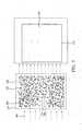
Fig. 1 is a schematic diagram depicting fabrication of a conventional color filter substrate by a spin coating process. Asubstrate 20 is disposed on asupport 12, and a firstcolor photoresist composition 13, provided by adispenser 11 of aspin coater 10, is injected on thesubstrate 20 having adisplay region 22 and aperipheral region 23. After spinning thesupport 12 as indicated by the arrow for a few seconds, a uniform coating of the first colorphotoresist composition 13 is formed on thesubstrate 20. The coating is then patterned to form a frontcolor filter pattern 30.Fig. 2 is a close-up view of location L shown inFig. 1 . The frontcolor filter pattern 30 formed on a dummy region of theperipheral region 23 has an opening 21. When forming a rearcolor filter pattern 40 on thedisplay region 22, a secondcolor photoresist composition 33 flows as indicated by the arrows over the frontcolor filter pattern 30. Since the second colorphotoresist composition 33 flowing into theopening 21 of the frontcolor filter pattern 30 is blocked by theboundary 25, a thicker rearcolor filter pattern 41 is formed, thereby producing an uneven rear color filter pattern 40 (comprising thicker rearcolor filter pattern 41 and thinner rear color filter pattern 42), further resulting in undesirable line mura defects of the full-color flat panel display.Fig. 3 is a photograph of a conventional full-color flat panel display, illustrating an example of such a line mura defect.US 5617230 discloses a color liquid crystal display device comprising light shielding layers and color filters on the inner surface of a cell, wherein similar light shielding layers and color filters are disposed also in a peripheral region outside of a display region which is equipped with groups of striped row and column electrodes opposed mutually to form pixels for display. The respective patterns of the light shielding layers and the color filters are the same in both the display region and the peripheral region. A liquid crystal layer formed in the display device has a twist angle of 160 DEG to 300 DEG , and a retardation compensator composed of a film is superposed on such layer so as to compensate the elliptical polarization. And a non-selective voltage is applied continuously to the scanning electrodes in the peripheral region so as to maintain the peripheral pixels in a light-shielded state, thereby rendering the display easier to be seen. Furthermore, due to overlaps of the color filters and the light shielding layers in both the display region and the peripheral region, the gap between the substrates is retained substantially uniform to minimize the nonuniformity of the backgroud color.US 5936694 (A ) discloses a liquid crystal device being constituted by disposing a liquid crystal between a pair of substrates each provided with an electrode to provide an effective optical modulation region and a peripheral region. At least one substrate of the pair of substrates comprises an intermediate layer disposed between the substrate and the electrode in the effective optical modulation region and the peripheral region, and the electrode on the intermediate layer comprises a first electrode disposed at least in the effective optical modulation region and a second electrode disposed in the peripheral region. The first and second electrodes are separated from each other. The intermediate layer may preferably include a color filter, a light-interrupting layer and a coating layer.US 2003 160916 (A1 ) discloses a color display device including: a first substrate and a second substrate opposing each other via a display medium layer interposed therebetween; a plurality of pixel electrodes arranged in a matrix pattern on one side of the first substrate; a common electrode formed on one side of the second substrate so as to oppose the plurality of pixel electrodes; and a plurality of color filter layers each having a different color formed between the second substrate and the common electrode. The common electrode and the color filter layers of different colors have a display area superposed on the plurality of pixel electrodes and a frame area outside a periphery of the display area. At least one of the plurality of color filter layers of different colors is continuous across a boundary between the display area and the frame area and is flat.- Systems for displaying images and methods for fabricating the same are provided. An exemplary embodiment of such system for displaying images is defined in
claim 1. - An exemplary embodiment of a method of fabricating a system for displaying images is defined in
claim 10. - A detailed description is given in the following with reference to the accompanying drawings.
- The invention can be more fully understood by reading the subsequent detailed description and examples with reference made to the accompanying drawings, wherein:
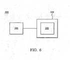
Fig. 1 is a schematic diagram for fabricating a conventional color filter substrate by a spin coating process.Fig. 2 is a close-up view schematic diagram of location L shown inFig. 1 Fig. 3 is a photograph of a conventional full-color flat panel display, illustrating line mura defect.Fig. 4 is a top-view schematic diagram of the system for displaying images according to an embodiment of the invention.Fig. 5 is a close-up view schematic diagram of location M shown inFig. 4 .Fig. 6 schematically shows another embodiment of a system for displaying images.- The following description is of the best-contemplated mode of carrying out the invention. This description is made for the purpose of illustrating the general principles of the invention and should not be taken in a limiting sense. The scope of the invention is best determined by reference to the appended claims.
- According to an embodiment of the invention, referring to
Fig. 4 , thesystem 100 for displaying images comprises asubstrate 110 having adisplay region 112 and aperipheral region 114. A full-color color filter pattern array comprising redcolor filter patterns 120R, greencolor filter patterns 120G, and bluecolor filter patterns 120B is formed on thedisplay region 112. Theperipheral region 114 has a dummy region, wherein one of the RGBcolor filter patterns color filter pattern 121 having an opening 123 serving as an alignment key or a test key.Fig. 5 is a close-up view of location M shown inFig. 4 . As shown inFig. 5 , the mosaiccolor filter pattern 121 formed on the dummy region comprises a plurality ofseparated pillars 126 and a plurality ofchannels 127 adjacent to thepillars 126, wherein the mosaiccolor filter pattern 121 is a front color filter pattern. Specifically, the volume ratio between the pillars and the channels is 1:5 to 2:1. The shapes of the pillars are unlimited, and can be cylinder shaped, square shaped or combinations thereof, for example and the dimension of the pillars is between 20 m x 20 m and 100 m x 100 m, for example. - When forming rear
color filter patterns 150 on thedisplay region 112 by a spin coating process, a colorphotoresist composition 140 flows as indicated by the arrows over the front color filter pattern. Since the front color filter pattern is a mosaiccolor filter pattern 121 having a plurality ofchannels 127 passing therethrough, thephotoresist composition 140 can flow through thechannels 127 to form the rearcolor filter patterns 150 seemingly without restriction even with the mosaiccolor filter pattern 121 incorporatingopening 123. Due to thechannels 127 of the mosaiccolor filter pattern 121, thecolor photoresist composition 140 can pass through the mosaiccolor filter pattern 121 to form of the rearcolor filter pattern 150 without the typical blocking effect being caused by the boundary 160. Therefore, the obtained rearcolor filter pattern 150 is relatively even film, thereby reducing or preventing a full-color flat panel display from presenting line mura defects. - In order to enable the
photoresist composition 140 to pass through the mosaiccolor filter pattern 121 without unwanted interference, the volume ratio between the pillars and the channels can be 1:5 to 2:1, preferably 1:3 to 1:1. Further, in order to maintain the function of the mosaic color filter pattern, the volume ratio between the pillars and the channels is equal to or more than 1:3. It should be noted that the methods for forming mosaic color filter patterns are not restricted to the representative example described above. By way of example, processes suitable to use in flat display panel fabrication, such as photolithography with a mosaic shadow mask, can be used. Further, a normal color filter pattern can be formed simultaneously on thedisplay region 112 of thesubstrate 110 when the mosaic color filter pattern is formed on theperipheral region 114. For example, the front color filter pattern comprising the normal color filter pattern withindisplay region 112 and the mosaic color filter pattern withinperipheral region 114 can be one of the RGBcolor filter patterns Fig. 6 schematically shows another embodiment of a system for displaying images which, in this case, is implemented as adisplay panel 200 or anelectronic device 400. The described active matrix organic electroluminescent device can be incorporated into a display panel that can be an OLED panel. As shown inFig. 6 , thedisplay panel 200 comprises an active matrix organic electroluminescent device, such as theorganic electroluminescent diode 100 shown inFig. 4 . Thedisplay panel 200 can form a portion of a variety of electronic devices (in this case, electronic device 400). Generally, theelectronic device 400 can comprise thedisplay panel 200 and aninput unit 300. Further, theinput unit 300 is operatively coupled to thedisplay panel 200 and provides input signals (e.g., an image signal) to thedisplay panel 200 to generate images. Theelectronic device 400 can be a mobile phone, digital camera, PDA (personal digital assistant), notebook computer, desktop computer, television, car display, or portable DVD player, for example.- While the invention has been described by way of example and in terms of the preferred embodiments, it is to be understood that the invention is not limited to the disclosed embodiments. To the contrary, it is intended to cover various modifications and similar arrangements (as would be apparent to those skilled in the ant). Therefore, the scope of the appended claims should be accorded the broadest interpretation so as to encompass all such modifications and similar arrangements.
Claims (11)
- A display substrate comprising:a substrate (110) having a display region (112) and a peripheral region (114); and a mosaic color filter pattern (121) formed on the peripheral region, comprising:a plurality of separated pillars(126); anda plurality of channels between (127) the pillars,characterised in thatthe plurality of separated pillars (126) and channels (127) is provided to attain a random positional distribution.
- The substrate as claimed in claim 1, wherein the mosaic color filter pattern is formed on a dummy region.
- The substrate as claimed in claim 1, wherein the mosaic color filter pattern has an opening.
- The substrate as claimed in claim 3, wherein the opening serves as an alignment key.
- The substrate as claimed in claim 1, further comprising a display panel (200), wherein the mosaic color filter pattern forms a portion of the display panel.
- The substrate as claimed in claim 5, further comprising an electronic device, wherein the electronic device comprises: the display panel(200); and
an input unit (300) coupled to the display panel operative to provide input to the display panel such that the display panel displays images. - The substrate as claimed in claim 6, wherein the electronic device is a mobile phone, digital camera, PDA (personal digital assistant), notebook computer, desktop computer, television, car display, or portable DVD player.
- The substrate as claimed in claim 1, wherein the volume ratio between the pillars and the channel is 1:5 to 2:1.
- The substrate as claimed in claim 8, wherein the mosaic color filter pattern has an opening serving as an alignment key.
- A method of fabricating a display substrate, comprising:providing a substrate (110) having a display region (112) and a peripheral region (114); and forming a mosaic color filter pattern on the peripheral region (114),wherein the mosaic color filter pattern (121) has a plurality of separated pillars(126) and a plurality of channels (127) between the pillars (126),characterised in that the plurality of separated pillars (126) and channels (127) is provided to attain a random positional distribution
- The method as claimed in claim 10, wherein the mosaic color filter pattern is formed by photolithography with a mosaic shadow mask.
Applications Claiming Priority (1)
| Application Number | Priority Date | Filing Date | Title |
|---|---|---|---|
| US11/670,549US7884899B2 (en) | 2007-02-02 | 2007-02-02 | System for displaying images and method with a peripheral region having a mosaic color filter pattern thereon that has pillars and channels and an opening along its boundary |
Publications (2)
| Publication Number | Publication Date |
|---|---|
| EP1953587A1 EP1953587A1 (en) | 2008-08-06 |
| EP1953587B1true EP1953587B1 (en) | 2012-11-21 |
Family
ID=39308020
Family Applications (1)
| Application Number | Title | Priority Date | Filing Date |
|---|---|---|---|
| EP08100512ACeasedEP1953587B1 (en) | 2007-02-02 | 2008-01-15 | Systems for displaying images and methods for fabricating the same |
Country Status (5)
| Country | Link |
|---|---|
| US (1) | US7884899B2 (en) |
| EP (1) | EP1953587B1 (en) |
| JP (1) | JP5311325B2 (en) |
| CN (1) | CN101236323B (en) |
| TW (1) | TWI385614B (en) |
Families Citing this family (2)
| Publication number | Priority date | Publication date | Assignee | Title |
|---|---|---|---|---|
| KR101564925B1 (en) | 2009-01-14 | 2015-11-03 | 삼성디스플레이 주식회사 | Color filter substrate and manufacturing method thereof |
| CN117893952B (en)* | 2024-03-15 | 2024-06-28 | 视睿(杭州)信息科技有限公司 | Video mosaic defect detection method based on deep learning |
Family Cites Families (12)
| Publication number | Priority date | Publication date | Assignee | Title |
|---|---|---|---|---|
| US5365357A (en)* | 1988-04-21 | 1994-11-15 | Asahi Glass Company Ltd. | Color liquid crystal display having color filters and light blocking layers in the periphery |
| JPH01293304A (en)* | 1988-05-23 | 1989-11-27 | Dainippon Printing Co Ltd | Production of color filter |
| US6061110A (en)* | 1994-10-18 | 2000-05-09 | Kabushiki Kaisha Toshiba | Reflection type liquid crystal display device and method of manufacturing the same |
| US5936694A (en)* | 1995-04-26 | 1999-08-10 | Canon Kabushiki Kaisha | Liquid crystal device and process for producing same |
| JPH0996716A (en)* | 1995-09-29 | 1997-04-08 | Toshiba Corp | Color filter substrate |
| JPH09197117A (en)* | 1996-01-19 | 1997-07-31 | Citizen Watch Co Ltd | Production of color filter |
| JP3859525B2 (en)* | 2002-02-28 | 2006-12-20 | シャープ株式会社 | Color display device |
| JP4055453B2 (en)* | 2002-04-02 | 2008-03-05 | 凸版印刷株式会社 | Manufacturing method of color filter for transflective color liquid crystal display device |
| US7612860B2 (en) | 2003-12-01 | 2009-11-03 | Lg Display Co., Ltd. | Color filter on thin film transistor type liquid crystal display device and method of fabricating the same with an alignment key formed with the orientation layer |
| TWI240107B (en)* | 2004-02-02 | 2005-09-21 | Toppoly Optoelectronics Corp | Transflective liquid crystal display |
| KR20060070346A (en)* | 2004-12-20 | 2006-06-23 | 삼성전자주식회사 | Display device |
| JP4235630B2 (en)* | 2005-07-11 | 2009-03-11 | 株式会社 日立ディスプレイズ | Color filter substrate and liquid crystal display device |
- 2007
- 2007-02-02USUS11/670,549patent/US7884899B2/enactiveActive
- 2007-12-26JPJP2007333575Apatent/JP5311325B2/ennot_activeExpired - Fee Related
- 2008
- 2008-01-03TWTW097100149Apatent/TWI385614B/ennot_activeIP Right Cessation
- 2008-01-10CNCN2008100006040Apatent/CN101236323B/enactiveActive
- 2008-01-15EPEP08100512Apatent/EP1953587B1/ennot_activeCeased
Also Published As
| Publication number | Publication date |
|---|---|
| CN101236323A (en) | 2008-08-06 |
| TW200834495A (en) | 2008-08-16 |
| CN101236323B (en) | 2012-12-26 |
| US7884899B2 (en) | 2011-02-08 |
| JP2008191651A (en) | 2008-08-21 |
| TWI385614B (en) | 2013-02-11 |
| JP5311325B2 (en) | 2013-10-09 |
| US20080186454A1 (en) | 2008-08-07 |
| EP1953587A1 (en) | 2008-08-06 |
Similar Documents
| Publication | Publication Date | Title |
|---|---|---|
| US20190251895A1 (en) | Pixel arrangement structure, metal mask, and display device | |
| EP1969400B1 (en) | Color filters for a rollable display | |
| US6738204B1 (en) | Arrangement of color elements for a color filter | |
| CN110850629A (en) | Color film substrate, display panel and display device | |
| US8619220B2 (en) | Liquid crystal display panel and color filter | |
| US7331286B2 (en) | Method for fabricating color filter of liquid crystal display device | |
| US7304698B2 (en) | Color filter substrate having dummy color filter in non-effective display area, and display device including the same | |
| US20250013096A1 (en) | Display substrate, display panel and display device | |
| US20070200980A1 (en) | Color display device | |
| EP1953587B1 (en) | Systems for displaying images and methods for fabricating the same | |
| WO2014176904A1 (en) | Display device, color film substrate and manufacturing method thereof | |
| US8508698B2 (en) | Dual-view display panel structure and method for producing the same | |
| US8179514B2 (en) | Liquid crystal display device with first and second protruding walls surrounding spherical spacers | |
| KR101570087B1 (en) | Liquid crystal display device | |
| US8605236B2 (en) | Liquid crystal display apparatus having color filter with color connection on black matrix and method of manufacturing the same | |
| US8144291B2 (en) | Display device and production method thereof | |
| KR20060134694A (en) | Mother board | substrate, the orientation film manufacturing apparatus formed on this mother board, and an orientation film manufacturing method | |
| KR20100057127A (en) | Color filter substrate and manufacturing method thereof | |
| KR20070030574A (en) | LCD and its manufacturing method | |
| JP2007121373A (en) | Liquid crystal display panel, color filter, and method of manufacturing color filter | |
| JP2008310256A (en) | Liquid crystal display device | |
| KR20070024178A (en) | Manufacturing Method Of Liquid Crystal Display | |
| KR20050017184A (en) | Liquid crystal display device and method of using the same | |
| KR20090043894A (en) | Color filter and its manufacturing method |
Legal Events
| Date | Code | Title | Description |
|---|---|---|---|
| PUAI | Public reference made under article 153(3) epc to a published international application that has entered the european phase | Free format text:ORIGINAL CODE: 0009012 | |
| AK | Designated contracting states | Kind code of ref document:A1 Designated state(s):AT BE BG CH CY CZ DE DK EE ES FI FR GB GR HR HU IE IS IT LI LT LU LV MC MT NL NO PL PT RO SE SI SK TR | |
| AX | Request for extension of the european patent | Extension state:AL BA MK RS | |
| 17P | Request for examination filed | Effective date:20090204 | |
| AKX | Designation fees paid | Designated state(s):DE FR GB IT NL | |
| 17Q | First examination report despatched | Effective date:20100811 | |
| GRAP | Despatch of communication of intention to grant a patent | Free format text:ORIGINAL CODE: EPIDOSNIGR1 | |
| RIN1 | Information on inventor provided before grant (corrected) | Inventor name:PENG, CHI-WEN Inventor name:CHEN, JR-HONG Inventor name:HSU, YAO-PIN Inventor name:CHEN, CHENG-HSIN | |
| GRAS | Grant fee paid | Free format text:ORIGINAL CODE: EPIDOSNIGR3 | |
| GRAA | (expected) grant | Free format text:ORIGINAL CODE: 0009210 | |
| AK | Designated contracting states | Kind code of ref document:B1 Designated state(s):DE FR GB IT NL | |
| RAP1 | Party data changed (applicant data changed or rights of an application transferred) | Owner name:CHIMEI INNOLUX CORPORATION | |
| REG | Reference to a national code | Ref country code:GB Ref legal event code:FG4D | |
| REG | Reference to a national code | Ref country code:DE Ref legal event code:R096 Ref document number:602008020192 Country of ref document:DE Effective date:20130117 | |
| REG | Reference to a national code | Ref country code:NL Ref legal event code:VDEP Effective date:20121121 | |
| PG25 | Lapsed in a contracting state [announced via postgrant information from national office to epo] | Ref country code:NL Free format text:LAPSE BECAUSE OF FAILURE TO SUBMIT A TRANSLATION OF THE DESCRIPTION OR TO PAY THE FEE WITHIN THE PRESCRIBED TIME-LIMIT Effective date:20121121 Ref country code:IT Free format text:LAPSE BECAUSE OF FAILURE TO SUBMIT A TRANSLATION OF THE DESCRIPTION OR TO PAY THE FEE WITHIN THE PRESCRIBED TIME-LIMIT Effective date:20121121 | |
| PLBE | No opposition filed within time limit | Free format text:ORIGINAL CODE: 0009261 | |
| STAA | Information on the status of an ep patent application or granted ep patent | Free format text:STATUS: NO OPPOSITION FILED WITHIN TIME LIMIT | |
| 26N | No opposition filed | Effective date:20130822 | |
| REG | Reference to a national code | Ref country code:DE Ref legal event code:R097 Ref document number:602008020192 Country of ref document:DE Effective date:20130822 | |
| REG | Reference to a national code | Ref country code:FR Ref legal event code:PLFP Year of fee payment:9 | |
| REG | Reference to a national code | Ref country code:FR Ref legal event code:PLFP Year of fee payment:10 | |
| REG | Reference to a national code | Ref country code:FR Ref legal event code:PLFP Year of fee payment:11 | |
| PGFP | Annual fee paid to national office [announced via postgrant information from national office to epo] | Ref country code:FR Payment date:20181213 Year of fee payment:12 | |
| PGFP | Annual fee paid to national office [announced via postgrant information from national office to epo] | Ref country code:GB Payment date:20190109 Year of fee payment:12 Ref country code:DE Payment date:20190102 Year of fee payment:12 | |
| REG | Reference to a national code | Ref country code:DE Ref legal event code:R119 Ref document number:602008020192 Country of ref document:DE | |
| GBPC | Gb: european patent ceased through non-payment of renewal fee | Effective date:20200115 | |
| PG25 | Lapsed in a contracting state [announced via postgrant information from national office to epo] | Ref country code:DE Free format text:LAPSE BECAUSE OF NON-PAYMENT OF DUE FEES Effective date:20200801 Ref country code:GB Free format text:LAPSE BECAUSE OF NON-PAYMENT OF DUE FEES Effective date:20200115 Ref country code:FR Free format text:LAPSE BECAUSE OF NON-PAYMENT OF DUE FEES Effective date:20200131 |