EP1949390B1 - A power converter - Google Patents
A power converterDownload PDFInfo
- Publication number
- EP1949390B1 EP1949390B1EP06807128AEP06807128AEP1949390B1EP 1949390 B1EP1949390 B1EP 1949390B1EP 06807128 AEP06807128 AEP 06807128AEP 06807128 AEP06807128 AEP 06807128AEP 1949390 B1EP1949390 B1EP 1949390B1
- Authority
- EP
- European Patent Office
- Prior art keywords
- power converter
- winding
- sub
- leg
- converter
- Prior art date
- Legal status (The legal status is an assumption and is not a legal conclusion. Google has not performed a legal analysis and makes no representation as to the accuracy of the status listed.)
- Ceased
Links
- 238000004804windingMethods0.000claimsabstractdescription68
- 230000005291magnetic effectEffects0.000claimsabstractdescription20
- 239000004020conductorSubstances0.000claimsdescription11
- 238000000034methodMethods0.000claimsdescription6
- 230000003472neutralizing effectEffects0.000claimsdescription2
- 238000013459approachMethods0.000description6
- YTBRNEUEFCNVHC-UHFFFAOYSA-N4,4'-dichlorobiphenylChemical compoundC1=CC(Cl)=CC=C1C1=CC=C(Cl)C=C1YTBRNEUEFCNVHC-UHFFFAOYSA-N0.000description3
- 239000003990capacitorSubstances0.000description2
- 238000004519manufacturing processMethods0.000description2
- 230000001360synchronised effectEffects0.000description2
- UXUFTKZYJYGMGO-CMCWBKRRSA-N(2s,3s,4r,5r)-5-[6-amino-2-[2-[4-[3-(2-aminoethylamino)-3-oxopropyl]phenyl]ethylamino]purin-9-yl]-n-ethyl-3,4-dihydroxyoxolane-2-carboxamideChemical compoundO[C@@H]1[C@H](O)[C@@H](C(=O)NCC)O[C@H]1N1C2=NC(NCCC=3C=CC(CCC(=O)NCCN)=CC=3)=NC(N)=C2N=C1UXUFTKZYJYGMGO-CMCWBKRRSA-N0.000description1
- RYGMFSIKBFXOCR-UHFFFAOYSA-NCopperChemical compound[Cu]RYGMFSIKBFXOCR-UHFFFAOYSA-N0.000description1
- 230000002411adverseEffects0.000description1
- 238000006243chemical reactionMethods0.000description1
- 238000010276constructionMethods0.000description1
- 229910052802copperInorganic materials0.000description1
- 239000010949copperSubstances0.000description1
- 238000010586diagramMethods0.000description1
- 230000005284excitationEffects0.000description1
- 239000011888foilSubstances0.000description1
- 230000007704transitionEffects0.000description1
Images


Classifications
- H—ELECTRICITY
- H01—ELECTRIC ELEMENTS
- H01F—MAGNETS; INDUCTANCES; TRANSFORMERS; SELECTION OF MATERIALS FOR THEIR MAGNETIC PROPERTIES
- H01F3/00—Cores, Yokes, or armatures
- H01F3/10—Composite arrangements of magnetic circuits
- H01F3/14—Constrictions; Gaps, e.g. air-gaps
- H—ELECTRICITY
- H01—ELECTRIC ELEMENTS
- H01F—MAGNETS; INDUCTANCES; TRANSFORMERS; SELECTION OF MATERIALS FOR THEIR MAGNETIC PROPERTIES
- H01F38/00—Adaptations of transformers or inductances for specific applications or functions
- H01F38/20—Instruments transformers
- H01F38/22—Instruments transformers for single phase AC
- H01F38/24—Voltage transformers
- H—ELECTRICITY
- H02—GENERATION; CONVERSION OR DISTRIBUTION OF ELECTRIC POWER
- H02M—APPARATUS FOR CONVERSION BETWEEN AC AND AC, BETWEEN AC AND DC, OR BETWEEN DC AND DC, AND FOR USE WITH MAINS OR SIMILAR POWER SUPPLY SYSTEMS; CONVERSION OF DC OR AC INPUT POWER INTO SURGE OUTPUT POWER; CONTROL OR REGULATION THEREOF
- H02M7/00—Conversion of AC power input into DC power output; Conversion of DC power input into AC power output
- H02M7/003—Constructional details, e.g. physical layout, assembly, wiring or busbar connections
- H—ELECTRICITY
- H01—ELECTRIC ELEMENTS
- H01F—MAGNETS; INDUCTANCES; TRANSFORMERS; SELECTION OF MATERIALS FOR THEIR MAGNETIC PROPERTIES
- H01F27/00—Details of transformers or inductances, in general
- H01F27/24—Magnetic cores
- H01F27/26—Fastening parts of the core together; Fastening or mounting the core on casing or support
- H01F27/263—Fastening parts of the core together
- H—ELECTRICITY
- H01—ELECTRIC ELEMENTS
- H01F—MAGNETS; INDUCTANCES; TRANSFORMERS; SELECTION OF MATERIALS FOR THEIR MAGNETIC PROPERTIES
- H01F27/00—Details of transformers or inductances, in general
- H01F27/28—Coils; Windings; Conductive connections
- H01F27/2804—Printed windings
- H—ELECTRICITY
- H05—ELECTRIC TECHNIQUES NOT OTHERWISE PROVIDED FOR
- H05K—PRINTED CIRCUITS; CASINGS OR CONSTRUCTIONAL DETAILS OF ELECTRIC APPARATUS; MANUFACTURE OF ASSEMBLAGES OF ELECTRICAL COMPONENTS
- H05K1/00—Printed circuits
- H05K1/16—Printed circuits incorporating printed electric components, e.g. printed resistor, capacitor, inductor
- H05K1/165—Printed circuits incorporating printed electric components, e.g. printed resistor, capacitor, inductor incorporating printed inductors
Definitions
- This inventionrelates to a power converter comprising a plurality of sub-converters and a magnetic core, the plurality of sub-converters each having a primary winding and a secondary winding, the magnetic core further comprising an E-core having a first end leg, a centre leg and a second end leg, both the first and second end legs having a gap formed therein.
- Power convertershave been known for a long time and are used to transform an input voltage, which may be a mains supply voltage or other power supply voltage into an output voltage more suitable for a particular load to be driven by the power converter.
- power convertersmay be used to transform the input mains voltage into voltages suitable for use with integrated circuits and other electronic equipment.
- Other power convertersare used to transform a DC intermediate drive voltage.
- One particularly useful approachhas been the usage of interleaved flyback converters with series connected primary windings.
- Another suitable approach other than the interleaved flyback converter approachis the current doubler approach. Both of these approaches are seen as effective and efficient for use with power converters.
- converters with such topologiescan be implemented using two magnetic elements. These magnetic elements may be combined quite readily into a single E-core where there is a gap in each outer leg and the centre leg has no gap. In the implementation of such a converter, it is important that there is minimal leakage inductance between the primary and secondary windings. In order to achieve this, the windings are interleaved so that the primary and secondary windings physically overlap to the maximum extent possible. This typically requires that the primary and secondary windings associated with each stage are wound around the outer leg in the E-core implementation with winding interleaved using planar or foil winding techniques as appropriate particularly for low voltage high current implementations.
- a power converterindicated generally by the reference numeral 1, comprising a plurality of sub-converters (not shown) and a magnetic core 3.
- the magnetic core 3comprises an E-core having a first outer leg 5, an inner leg 7 and a second outer leg 9. Both the first and second outer legs 5, 9 have a gap 11, 13 respectively, formed therein.
- the magnetic core 3is mounted on a printed circuit board (PCB) 15 having a plurality of layers (not shown).
- PCBprinted circuit board
- the power converter 1comprises a plurality of sub-converters each having a primary winding 17, 19 and a secondary winding (not shown).
- the primary winding 17 of a first sub-converteris wound around the first outer leg 5 of the magnetic core 3 and a primary winding 19 of a second sub-converter is wound around the second outer leg 9 of the magnetic core.
- the pair of primary windings 17, 19are formed from a unitary winding of conductive material 21.
- the unitary winding of conductive material 21 forming the pair of primary windings 17, 19,is led around the first outer leg 5 in a first orientation, in this case anti-clockwise, back between the first outer leg 5 and the inner leg 7, around the inner leg 7 in a second orientation (clockwise) opposite to the first orientation, back between the inner leg 7 and the second outer leg 9 and around the second outer leg 9 in the first orientation.
- Each end 23, 25 of the unitary winding of conductive material 21terminates in a vias 27, 29 respectively.
- the vias 27, 29are located in a corner 30 location of the PCB 15. Therefore, the unitary winding of conductive material 21 forms a single strip of conductive material that follows a labyrinthine route through the legs 5, 7, 9 of the power converter and substantially surrounds both of the outer legs 5, 9.
- the power converter 1further comprises means to manage common-mode noise, which comprises a dummy winding 31 having at least one turn 32 connected to a neutralising capacitive element 33.
- the dummy winding 31has a number of turns comparable to the number of turns of the primary winding of one of the sub-converters.
- the turns of the dummy winding 31are placed around the inner leg 7 of the magnetic core 3.
- a resistive element 35 and a capacitive element 37are mounted on the PCB 15 and are provided for turning the cancellation properties and/or to limit ringing in the power converter.
- resistive element 35 and the capacitive element 37may be provided for this purpose.
- the turn 32 of the dummy winding 31has been shown mounted on the surface of the PCB is and indeed this turn 32 has been shown exaggerated, protruding upwardly from the surface of the PCB 15 for reasons of clarity and it will be understood that when using planar techniques the turn will in fact be a relatively thin layer of conductive material on a layer of the PCB.
- the dummy windingis connected in series with the cancellation capacitance which can be implemented as a discrete part as shown or by utilising the capacitance between copper planes in the PCB.
- the value of the capacitancecan be trimmed or reduced by adding another series element.
- a resistorcan be fitted in series to reduce any tendency for the dummy winding and PCB capacitance to ring at higher frequencies. All elements in the above common-mode noise management circuit may therefore be connected in series.
- the dummy winding 31wound around the centre leg 7 a very compact device may be provided that would be well balanced and efficient in use. Furthermore, the dummy winding 31 will not cause to reduce the size of the other windings 17, 19 that are current carrying windings. This is particularly useful as the efficiency of the power converter 1 is not affected adversely. In the embodiments shown the power converter 1 is shown using planar techniques but it will be understood that wire wound techniques could also be used for certain or all of the portions of the invention.
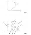
- a ramp voltage 41used for control of pre-bias operation in the power converter.
- the use of pre-bias controlensures that sinking current is not drawn from the output during start-up until the output is running at between 70 to 100% of the required output voltage.
- the ramp voltage 41may be derived simply by charging a capacitor (not shown) to provide a suitable approximation of the desired ramp.
- the desired voltages for the gate drive and the output voltage settingmay be derived from the ramp voltage 41.
- FIG. 5 of the drawingsthere is shown a diagrammatic representation of the circuit schematic for control of the pre-bias operation in the power converter.
- a voltage source 43which represents the ramp voltage created using a current source and a capacitor (both of which are not shown for clarity), is provided along with resistive components 45, 47, 49 and 51 as well as zener diode 53. From this circuit, the peak gate drive that is proportional to voltage on line 55, and the output proportional to voltage on line 57, may be obtained.
- the circuit shownwill allow a smooth ramp to be produced at.a relatively low cost.
- two ramp slopes(not shown), one of which allows for a soft transition of the gate drives of the synchronous rectifier elements (not shown) of the power converter from initially diode mode operation to synchronous rectifier operation could also be provided.
- the power converter 1has three legs in total including an inner leg 7 and a pair of outer legs 5, 9. It will be understood that this is a particular type of star configuration of a converter magnetic core 3 with two outer legs, which may also be referred to as poles, and an inner leg. Other star configurations with more than two outer legs (poles) could also be provided and indeed are intended to be covered within the scope of this specification and the appended claims.
- a power converter with a magnetic core having an inner leg and three outer legs (poles), the three outer legs being evenly spaced from the inner leg and evenly spaced from each other symmetrically around the centre legis also envisaged.
- the three outer legsare separated by 120° with respect to each of the other outer legs around the inner leg.
- a power converter with an X-corethe X-core having an inner leg and four outer legs (poles) evenly spaced from each other symmetrically about the inner leg, separated 90° from adjacent outer legs, and so on and the example with two outer legs has been shown for convenience and illustrative purposes only.
- windings on the outer legshave been described as separate sub-converters, it will be understood that typically, these sub-converters are not entirely separate and in fact are interleaved and in a normal embodiment the outputs of the sub-converters will be combined together for a single power converter output.
- the componentshave been described in this instance as sub-converters for reasons of convenience and clarity.
Landscapes
- Engineering & Computer Science (AREA)
- Power Engineering (AREA)
- Chemical & Material Sciences (AREA)
- Composite Materials (AREA)
- Dc-Dc Converters (AREA)
- Coils Of Transformers For General Uses (AREA)
- Amplifiers (AREA)
- Control Of Eletrric Generators (AREA)
Abstract
Description
- This invention relates to a power converter comprising a plurality of sub-converters and a magnetic core, the plurality of sub-converters each having a primary winding and a secondary winding, the magnetic core further comprising an E-core having a first end leg, a centre leg and a second end leg, both the first and second end legs having a gap formed therein.
- Power converters have been known for a long time and are used to transform an input voltage, which may be a mains supply voltage or other power supply voltage into an output voltage more suitable for a particular load to be driven by the power converter. Typically, power converters may be used to transform the input mains voltage into voltages suitable for use with integrated circuits and other electronic equipment. Other power converters are used to transform a DC intermediate drive voltage. Heretofore, there have been many different topologies used for effecting the power conversion. One particularly useful approach has been the usage of interleaved flyback converters with series connected primary windings. Another suitable approach other than the interleaved flyback converter approach is the current doubler approach. Both of these approaches are seen as effective and efficient for use with power converters.
- One feature of both of these approaches, is that converters with such topologies can be implemented using two magnetic elements. These magnetic elements may be combined quite readily into a single E-core where there is a gap in each outer leg and the centre leg has no gap. In the implementation of such a converter, it is important that there is minimal leakage inductance between the primary and secondary windings. In order to achieve this, the windings are interleaved so that the primary and secondary windings physically overlap to the maximum extent possible. This typically requires that the primary and secondary windings associated with each stage are wound around the outer leg in the E-core implementation with winding interleaved using planar or foil winding techniques as appropriate particularly for low voltage high current implementations. For example the paper byJIAN SUN ET AL: "Orthogonal winding structures and design for planar integrated magnetics" APPLIED POWER ELECTRONICS CONFERENCE AND EXPOSITION, 2004. APEC '04. NINETEENTH ANNUAL IEEE ANAHEIM, CA, USA 22-26 FEB. 2004, PISCATAWAY, NJ, USA, IEEE, 22 February 2004 (2004-02-22), pages 933-938, there is described a current doubling arrangement of the type.
- There have been provided various converters in which there is supplied a primary winding around each leg with the windings then connected in series with respect to each other. However there are numerous difficulties with such an implementation. Typically, this implementation requires additional interconnects between layers of a winding. These are usually implemented using via holes placed in the printed circuit board (PCB). However, placement of via holes is very difficult and it is important to maintain agency-mandated spacings between input and output connections in the converter. A partial solution involves the use of buried and/or blind vias. This however is undesirable due to the addition of extra processing steps in the manufacture of the PCB which further increases the cost of the PCB fabrication process.
- Another problem with the known implementations of converter such as those described above, and in particular implementations with half-bridge primary excitation, is that these implementations are unbalanced in the context of generating common-mode electromagnetic interference (EMI). In a common mode noise management sense it is very desirable that a balanced condition exists so that the net common mode current flowing is minimised. One solution that has been suggested is to provide dummy noise-cancelling windings in either printed circuit board transformer implementations or in implementations using wound transformers. Although effective, this implementation takes up significant space within a transformer which is highly undesirable in the modern age of minimisation of electronic components in general. Having dummy windings whose sole purpose is for noise cancellation and which do not carry current can also add to leakage inductance in the converter. By providing additional dummy windings, the space provided for active current carrying windings is reduced thereby necessitating smaller active windings which are inherently more resistive which adds to the overall losses and reduces the efficiency of the converter.
- According to the invention there is provided a power converter as defined by the appended claims.
- The invention will now be more clearly understood from the following description of an embodiment thereof given by way of example only with reference to the accompanying drawings in which:-
Fig. 1 is a side cross-sectional view of a power converter E-core mounted on a printed circuit board;Fig. 2 is a plan cross-sectional view of a primary winding for a converter according to the present invention;Fig. 3 is a side cross-sectional view of an alternative embodiment of power converter with means to manage common-mode noise;Fig. 4 is a diagrammatic representation of a ramp used for the control of pre-bias operation; andFig. 5 is a block diagram of a circuit used for generating the ramp voltage.- Referring to the drawings and initially to
Fig. 1 thereof there is shown a power converter indicated generally by thereference numeral 1, comprising a plurality of sub-converters (not shown) and amagnetic core 3. Themagnetic core 3 comprises an E-core having a firstouter leg 5, aninner leg 7 and a secondouter leg 9. Both the first and secondouter legs gap magnetic core 3 is mounted on a printed circuit board (PCB) 15 having a plurality of layers (not shown). - Referring to
Fig. 2 of the drawings, where like parts have been given the same reference numeral as before, there is shown a plan cross-sectional view of the power converter taken along the lines "A-A" ofFig. 1 . Thepower converter 1 comprises a plurality of sub-converters each having aprimary winding primary winding 17 of a first sub-converter is wound around the firstouter leg 5 of themagnetic core 3 and aprimary winding 19 of a second sub-converter is wound around the secondouter leg 9 of the magnetic core. The pair ofprimary windings conductive material 21. The unitary winding ofconductive material 21 forming the pair ofprimary windings outer leg 5 in a first orientation, in this case anti-clockwise, back between the firstouter leg 5 and theinner leg 7, around theinner leg 7 in a second orientation (clockwise) opposite to the first orientation, back between theinner leg 7 and the secondouter leg 9 and around the secondouter leg 9 in the first orientation. Eachend 23, 25 of the unitary winding ofconductive material 21 terminates in avias vias conductive material 21 forms a single strip of conductive material that follows a labyrinthine route through thelegs outer legs - Referring to
Figure 3 of the drawings, there is shown an alternative embodiment of power converter according to the present invention, where like parts have been given the same reference numerals as before. Thepower converter 1 further comprises means to manage common-mode noise, which comprises a dummy winding 31 having at least oneturn 32 connected to a neutralisingcapacitive element 33. Preferably, the dummy winding 31 has a number of turns comparable to the number of turns of the primary winding of one of the sub-converters. The turns of the dummy winding 31 are placed around theinner leg 7 of themagnetic core 3. In addition to these components, aresistive element 35 and acapacitive element 37 are mounted on thePCB 15 and are provided for turning the cancellation properties and/or to limit ringing in the power converter. It will be understood that either or both of theresistive element 35 and thecapacitive element 37 may be provided for this purpose. Furthermore, for reasons of clarity, only oneturn 32 of the dummy winding 31 has been shown mounted on the surface of the PCB is and indeed thisturn 32 has been shown exaggerated, protruding upwardly from the surface of thePCB 15 for reasons of clarity and it will be understood that when using planar techniques the turn will in fact be a relatively thin layer of conductive material on a layer of the PCB. - The dummy winding is connected in series with the cancellation capacitance which can be implemented as a discrete part as shown or by utilising the capacitance between copper planes in the PCB. The value of the capacitance can be trimmed or reduced by adding another series element. Alternatively, a resistor can be fitted in series to reduce any tendency for the dummy winding and PCB capacitance to ring at higher frequencies. All elements in the above common-mode noise management circuit may therefore be connected in series.
- By having the dummy winding 31 wound around the centre leg 7 a very compact device may be provided that would be well balanced and efficient in use. Furthermore, the dummy winding 31 will not cause to reduce the size of the
other windings power converter 1 is not affected adversely. In the embodiments shown thepower converter 1 is shown using planar techniques but it will be understood that wire wound techniques could also be used for certain or all of the portions of the invention. - Referring to
Fig. 4 of the drawings there is shown aramp voltage 41 used for control of pre-bias operation in the power converter. The use of pre-bias control ensures that sinking current is not drawn from the output during start-up until the output is running at between 70 to 100% of the required output voltage. Theramp voltage 41 may be derived simply by charging a capacitor (not shown) to provide a suitable approximation of the desired ramp. The desired voltages for the gate drive and the output voltage setting may be derived from theramp voltage 41. - Referring to
Fig. 5 of the drawings there is shown a diagrammatic representation of the circuit schematic for control of the pre-bias operation in the power converter. Avoltage source 43, which represents the ramp voltage created using a current source and a capacitor (both of which are not shown for clarity), is provided along withresistive components zener diode 53. From this circuit, the peak gate drive that is proportional to voltage online 55, and the output proportional to voltage online 57, may be obtained. Essentially, we wish to provide a relatively smooth ramp for control of the pre-bias operation as well as provide an inexpensive control circuit. The circuit shown will allow a smooth ramp to be produced at.a relatively low cost. Alternatively, it is envisaged that two ramp slopes (not shown), one of which allows for a soft transition of the gate drives of the synchronous rectifier elements (not shown) of the power converter from initially diode mode operation to synchronous rectifier operation could also be provided. - It will be understood that in the embodiments shown above, in addition to providing gaps in the E-core and a continuous
inner leg 7, it will be understood that the gap may alternatively be implemented by abutting a separate section, such as a planar section, up against an extendedinner leg 7. Furthermore, in the embodiments shown and described above, thepower converter 1 has three legs in total including aninner leg 7 and a pair ofouter legs magnetic core 3 with two outer legs, which may also be referred to as poles, and an inner leg. Other star configurations with more than two outer legs (poles) could also be provided and indeed are intended to be covered within the scope of this specification and the appended claims. For example, a power converter with a magnetic core having an inner leg and three outer legs (poles), the three outer legs being evenly spaced from the inner leg and evenly spaced from each other symmetrically around the centre leg is also envisaged. In this embodiment, the three outer legs are separated by 120° with respect to each of the other outer legs around the inner leg. Furthermore, it is envisaged that there could be provided a power converter with an X-core, the X-core having an inner leg and four outer legs (poles) evenly spaced from each other symmetrically about the inner leg, separated 90° from adjacent outer legs, and so on and the example with two outer legs has been shown for convenience and illustrative purposes only. - Furthermore, although throughout the description, the windings on the outer legs have been described as separate sub-converters, it will be understood that typically, these sub-converters are not entirely separate and in fact are interleaved and in a normal embodiment the outputs of the sub-converters will be combined together for a single power converter output. The components have been described in this instance as sub-converters for reasons of convenience and clarity.
- In this specification the terms "comprise", "comprises", "comprised" and "comprising" are deemed totally interchangeable and the terms "include", "includes", "included" and '"including" are deemed totally interchangeable and should be afforded the widest possible interpretation.
- The invention is in no way limited to the embodiments hereinbefore described but may be varied in both construction and detail within the scope of the claims.
Claims (11)
- A power converter (1) comprising a plurality of sub-converters and a magnetic core (3), the plurality of sub-converters each having a primary winding (17, 19) and a secondary winding, the magnetic core (3) further comprising an inner leg (7) and a plurality of outer legs (5, 9), each of the plurality of outer legs (5, 9) having a gap (11, 13) formed therein, arranged such that the primary windings (17, 19) of a plurality of the sub-converters each comprise a plurality of turns, each turn of one of the sub-converters being formed from a unitary winding of conductive material (21) with a corresponding turn of another sub-converter, each turn of the sub-converter being connected to another turn of that sub-converter by way of an interconnect, thereby connecting the primary windings of the sub-converters in series on a tum-by-tum basis and wherein the primary winding (17) of one of the sub-converters is wound around one of the outer legs (5) and the primary winding (19) of another sub-converter is wound around another of the outer legs (9), the primary windings (17, 19) being formed from a unitary winding of conductive material (21) which is wound around each of the outer legs and the inner leg (7), the unitary winding being wound at least partially around the inner leg between being wound around a pair of outer legs.
- A power converter (1) as claimed in claim 1 in which the power converter further comprises a printed circuit board (PCB) (15) and the primary windings are constructed using planar techniques.
- A power converter (1) as claimed in claim 2 in which each end (23, 25) of the unitary winding of conductive material (21) terminates in a vias (27, 29).
- A power converter (1) as claimed in claim 3 in which the vias (27, 29) are located in a corner location of the PCB (15).
- A power converter (1) as claimed in any preceding claim in which the magnetic core (3) further comprises an E-core having a first outer leg (5), an inner leg (7) and a second outer leg (9).
- A power converter (1) as claimed in claim 5 in which the unitary winding of conductive material (21) is led around the first outer leg (5) in a first orientation, back between the first outer leg (5) and the inner leg (7), around the inner leg (7) in the opposite orientation to the first orientation, back between the inner leg (7) and the second outer leg (9) and around the second outer leg (9) in the first orientation.
- A power converter (1) as claimed in claim 7 in which the unitary winding of conductive material (21) substantially surrounds each of the outer legs (5, 9).
- A power converter (1) as claimed in any of claims 1 to 4 in which the magnetic core (3) further comprises a star configuration core in which there are provided three or more outer legs and an inner leg (7), the outer legs being evenly spaced from the inner leg and symmetrically spaced around the inner leg with respect to each other.
- A power converter (1) as claimed in any preceding claim in which the power converter is further provided with means to manage common-mode noise, the means comprising a dummy winding (31) having at least one turn (32), the turn being connected to a neutralising capacitive element (33).
- A power converter (1) as claimed in claim 9 in which the dummy winding (31) has a number of turns (32) comparable to the number of turns of the primary winding (17, 19) of a sub-converter of the power converter.
- A power converter (1) as claimed in claim 9 or 10 in which the turn (32) of the dummy winding (31) is placed around the inner leg (7) of the magnetic core (3).
Applications Claiming Priority (2)
| Application Number | Priority Date | Filing Date | Title |
|---|---|---|---|
| IE20050684 | 2005-10-10 | ||
| PCT/EP2006/067247WO2007042519A2 (en) | 2005-10-10 | 2006-10-10 | A power converter |
Publications (2)
| Publication Number | Publication Date |
|---|---|
| EP1949390A2 EP1949390A2 (en) | 2008-07-30 |
| EP1949390B1true EP1949390B1 (en) | 2011-01-05 |
Family
ID=37801404
Family Applications (1)
| Application Number | Title | Priority Date | Filing Date |
|---|---|---|---|
| EP06807128ACeasedEP1949390B1 (en) | 2005-10-10 | 2006-10-10 | A power converter |
Country Status (7)
| Country | Link |
|---|---|
| US (1) | US20090040001A1 (en) |
| EP (1) | EP1949390B1 (en) |
| CN (1) | CN101356594B (en) |
| AT (1) | ATE494619T1 (en) |
| DE (1) | DE602006019471D1 (en) |
| IE (1) | IES20060738A2 (en) |
| WO (1) | WO2007042519A2 (en) |
Families Citing this family (4)
| Publication number | Priority date | Publication date | Assignee | Title |
|---|---|---|---|---|
| KR101133397B1 (en)* | 2010-04-05 | 2012-04-09 | 삼성전기주식회사 | Planar transformer and manufacturing method thereof |
| US9053845B2 (en) | 2012-06-12 | 2015-06-09 | General Electric Company | Transformer with planar primary winding |
| JP6635306B2 (en)* | 2016-09-21 | 2020-01-22 | 株式会社オートネットワーク技術研究所 | Magnetic core for reactors and reactors |
| CN114050026B (en)* | 2021-11-30 | 2024-06-11 | 杭州云电科技能源有限公司 | Magnetic assembly, manufacturing method thereof, power module and switching power supply |
Family Cites Families (20)
| Publication number | Priority date | Publication date | Assignee | Title |
|---|---|---|---|---|
| US1376978A (en)* | 1917-11-24 | 1921-05-03 | Cutler Hammer Mfg Co | Regulator for alternating currents |
| GB1384950A (en)* | 1971-05-05 | 1975-02-26 | Commerzstahl Handel | Transformer |
| US4378522A (en)* | 1981-04-30 | 1983-03-29 | Suladze Robert N | Adjustable current source |
| US5555494A (en)* | 1993-09-13 | 1996-09-10 | Morris; George Q. | Magnetically integrated full wave DC to DC converter |
| US5426409A (en)* | 1994-05-24 | 1995-06-20 | The United States Of America As Represented By The Secretary Of The Navy | Current controlled variable inductor |
| US6366062B2 (en)* | 1997-12-08 | 2002-04-02 | Microplanet, Inc. | Method and apparatus for electronic power control |
| US6377155B1 (en)* | 1995-10-10 | 2002-04-23 | Georgia Tech Research Corp. | Microfabricated electromagnetic system and method for forming electromagnets in microfabricated devices |
| US6160303A (en)* | 1997-08-29 | 2000-12-12 | Texas Instruments Incorporated | Monolithic inductor with guard rings |
| US6591091B1 (en)* | 1998-11-12 | 2003-07-08 | Broadcom Corporation | System and method for coarse/fine PLL adjustment |
| JP2000260639A (en)* | 1999-03-11 | 2000-09-22 | Murata Mfg Co Ltd | Coil device and switching power supply device |
| US6400249B1 (en)* | 2000-12-18 | 2002-06-04 | Ascom Energy Systems Ag | Transformer providing low output voltage |
| DE10139707A1 (en)* | 2001-08-11 | 2003-02-20 | Philips Corp Intellectual Pty | circuit board |
| US6727793B2 (en)* | 2001-08-21 | 2004-04-27 | Astec International Limited | Low-power transformer for printed circuit boards |
| US6490181B1 (en)* | 2001-08-24 | 2002-12-03 | The University Of Hong Kong | Apparatus for reducing common mode noise current in power converters |
| US6563718B1 (en)* | 2001-12-06 | 2003-05-13 | Koninklijke Philips Electronics N.V. | Capacitively coupled power converter |
| US20030123174A1 (en)* | 2001-12-28 | 2003-07-03 | Mark Hennecken | Continuously variable storage device data transfer rate |
| US6549436B1 (en)* | 2002-02-21 | 2003-04-15 | Innovative Technology Licensing Llc | Integrated magnetic converter circuit and method with improved filtering |
| US6937115B2 (en)* | 2002-02-25 | 2005-08-30 | Massachusetts Institute Of Technology | Filter having parasitic inductance cancellation |
| US6801146B2 (en)* | 2002-11-14 | 2004-10-05 | Fyre Storm, Inc. | Sample and hold circuit including a multiplexer |
| US7427910B2 (en)* | 2004-08-19 | 2008-09-23 | Coldwatt, Inc. | Winding structure for efficient switch-mode power converters |
- 2006
- 2006-10-10WOPCT/EP2006/067247patent/WO2007042519A2/enactiveApplication Filing
- 2006-10-10CNCN2006800462381Apatent/CN101356594B/enactiveActive
- 2006-10-10IEIE20060738Apatent/IES20060738A2/ennot_activeIP Right Cessation
- 2006-10-10EPEP06807128Apatent/EP1949390B1/ennot_activeCeased
- 2006-10-10ATAT06807128Tpatent/ATE494619T1/ennot_activeIP Right Cessation
- 2006-10-10USUS12/089,748patent/US20090040001A1/ennot_activeAbandoned
- 2006-10-10DEDE602006019471Tpatent/DE602006019471D1/enactiveActive
Also Published As
| Publication number | Publication date |
|---|---|
| ATE494619T1 (en) | 2011-01-15 |
| WO2007042519A3 (en) | 2007-11-08 |
| EP1949390A2 (en) | 2008-07-30 |
| DE602006019471D1 (en) | 2011-02-17 |
| US20090040001A1 (en) | 2009-02-12 |
| CN101356594A (en) | 2009-01-28 |
| IES20060738A2 (en) | 2007-09-05 |
| WO2007042519A2 (en) | 2007-04-19 |
| CN101356594B (en) | 2012-04-25 |
Similar Documents
| Publication | Publication Date | Title |
|---|---|---|
| US11121633B2 (en) | Low common mode noise transformers and switch-mode DC-DC power converters | |
| US7671713B2 (en) | Integrated structure of passive elements in LLC resonance converter realized by flexible circuit boards | |
| KR102020648B1 (en) | Transformer and LLC Resonant Converter having the same | |
| US6124778A (en) | Magnetic component assembly | |
| US7427910B2 (en) | Winding structure for efficient switch-mode power converters | |
| US8847719B2 (en) | Transformer with split primary winding | |
| US7554430B2 (en) | Vertical winding structures for planar magnetic switched-mode power converters | |
| US20190122814A1 (en) | Capacitive reactance voltage transformer | |
| US11398344B2 (en) | Transformer | |
| EP3267569A1 (en) | Isolated switching power source | |
| US20120119676A1 (en) | Flyback power converter with divided energy transfer element | |
| US9722499B2 (en) | Energy transfer element with capacitor compensated cancellation and balance shield windings | |
| CN113950727A (en) | Stacked matrix transformer | |
| EP1949390B1 (en) | A power converter | |
| JP3196187B2 (en) | Mounting structure of electromagnetic circuit | |
| WO2006007238A3 (en) | Dc/dc converter with multiple mutually-isolated power sources | |
| US8305183B2 (en) | Transformer for multi-output power supplies | |
| WO2008027166A2 (en) | Transformers with improved voltage-step-down ratios and dc-to-dc power converters employing same | |
| CN113168956B (en) | Low-height coupled inductor | |
| US6275396B1 (en) | Power feed for a submarine communications system | |
| JP2002299130A (en) | Composite element for power source | |
| CN219180333U (en) | PCB board transformer coil board and PCB board transformer | |
| IE20060739A1 (en) | A power converter | |
| JP3823322B2 (en) | Distributed constant structure | |
| US6930894B2 (en) | Switching power supply and distributed parameter structure |
Legal Events
| Date | Code | Title | Description |
|---|---|---|---|
| PUAI | Public reference made under article 153(3) epc to a published international application that has entered the european phase | Free format text:ORIGINAL CODE: 0009012 | |
| 17P | Request for examination filed | Effective date:20080512 | |
| AK | Designated contracting states | Kind code of ref document:A2 Designated state(s):AT BE BG CH CY CZ DE DK EE ES FI FR GB GR HU IE IS IT LI LT LU LV MC NL PL PT RO SE SI SK TR | |
| 17Q | First examination report despatched | Effective date:20080805 | |
| RAP1 | Party data changed (applicant data changed or rights of an application transferred) | Owner name:TEXAS INSTRUMENTS (CORK) LIMITED | |
| GRAP | Despatch of communication of intention to grant a patent | Free format text:ORIGINAL CODE: EPIDOSNIGR1 | |
| DAX | Request for extension of the european patent (deleted) | ||
| GRAS | Grant fee paid | Free format text:ORIGINAL CODE: EPIDOSNIGR3 | |
| GRAA | (expected) grant | Free format text:ORIGINAL CODE: 0009210 | |
| AK | Designated contracting states | Kind code of ref document:B1 Designated state(s):AT BE BG CH CY CZ DE DK EE ES FI FR GB GR HU IE IS IT LI LT LU LV MC NL PL PT RO SE SI SK TR | |
| REG | Reference to a national code | Ref country code:GB Ref legal event code:FG4D | |
| REG | Reference to a national code | Ref country code:CH Ref legal event code:EP | |
| REG | Reference to a national code | Ref country code:IE Ref legal event code:FG4D | |
| REF | Corresponds to: | Ref document number:602006019471 Country of ref document:DE Date of ref document:20110217 Kind code of ref document:P | |
| REG | Reference to a national code | Ref country code:DE Ref legal event code:R096 Ref document number:602006019471 Country of ref document:DE Effective date:20110217 | |
| REG | Reference to a national code | Ref country code:NL Ref legal event code:T3 | |
| PG25 | Lapsed in a contracting state [announced via postgrant information from national office to epo] | Ref country code:SI Free format text:LAPSE BECAUSE OF FAILURE TO SUBMIT A TRANSLATION OF THE DESCRIPTION OR TO PAY THE FEE WITHIN THE PRESCRIBED TIME-LIMIT Effective date:20110105 | |
| LTIE | Lt: invalidation of european patent or patent extension | Effective date:20110105 | |
| PG25 | Lapsed in a contracting state [announced via postgrant information from national office to epo] | Ref country code:PT Free format text:LAPSE BECAUSE OF FAILURE TO SUBMIT A TRANSLATION OF THE DESCRIPTION OR TO PAY THE FEE WITHIN THE PRESCRIBED TIME-LIMIT Effective date:20110505 Ref country code:LV Free format text:LAPSE BECAUSE OF FAILURE TO SUBMIT A TRANSLATION OF THE DESCRIPTION OR TO PAY THE FEE WITHIN THE PRESCRIBED TIME-LIMIT Effective date:20110105 Ref country code:GR Free format text:LAPSE BECAUSE OF FAILURE TO SUBMIT A TRANSLATION OF THE DESCRIPTION OR TO PAY THE FEE WITHIN THE PRESCRIBED TIME-LIMIT Effective date:20110406 Ref country code:SE Free format text:LAPSE BECAUSE OF FAILURE TO SUBMIT A TRANSLATION OF THE DESCRIPTION OR TO PAY THE FEE WITHIN THE PRESCRIBED TIME-LIMIT Effective date:20110105 Ref country code:IS Free format text:LAPSE BECAUSE OF FAILURE TO SUBMIT A TRANSLATION OF THE DESCRIPTION OR TO PAY THE FEE WITHIN THE PRESCRIBED TIME-LIMIT Effective date:20110505 Ref country code:LT Free format text:LAPSE BECAUSE OF FAILURE TO SUBMIT A TRANSLATION OF THE DESCRIPTION OR TO PAY THE FEE WITHIN THE PRESCRIBED TIME-LIMIT Effective date:20110105 Ref country code:ES Free format text:LAPSE BECAUSE OF FAILURE TO SUBMIT A TRANSLATION OF THE DESCRIPTION OR TO PAY THE FEE WITHIN THE PRESCRIBED TIME-LIMIT Effective date:20110416 | |
| PG25 | Lapsed in a contracting state [announced via postgrant information from national office to epo] | Ref country code:PL Free format text:LAPSE BECAUSE OF FAILURE TO SUBMIT A TRANSLATION OF THE DESCRIPTION OR TO PAY THE FEE WITHIN THE PRESCRIBED TIME-LIMIT Effective date:20110105 Ref country code:AT Free format text:LAPSE BECAUSE OF FAILURE TO SUBMIT A TRANSLATION OF THE DESCRIPTION OR TO PAY THE FEE WITHIN THE PRESCRIBED TIME-LIMIT Effective date:20110105 Ref country code:FI Free format text:LAPSE BECAUSE OF FAILURE TO SUBMIT A TRANSLATION OF THE DESCRIPTION OR TO PAY THE FEE WITHIN THE PRESCRIBED TIME-LIMIT Effective date:20110105 Ref country code:CY Free format text:LAPSE BECAUSE OF FAILURE TO SUBMIT A TRANSLATION OF THE DESCRIPTION OR TO PAY THE FEE WITHIN THE PRESCRIBED TIME-LIMIT Effective date:20110105 Ref country code:BG Free format text:LAPSE BECAUSE OF FAILURE TO SUBMIT A TRANSLATION OF THE DESCRIPTION OR TO PAY THE FEE WITHIN THE PRESCRIBED TIME-LIMIT Effective date:20110405 Ref country code:BE Free format text:LAPSE BECAUSE OF FAILURE TO SUBMIT A TRANSLATION OF THE DESCRIPTION OR TO PAY THE FEE WITHIN THE PRESCRIBED TIME-LIMIT Effective date:20110105 | |
| PG25 | Lapsed in a contracting state [announced via postgrant information from national office to epo] | Ref country code:EE Free format text:LAPSE BECAUSE OF FAILURE TO SUBMIT A TRANSLATION OF THE DESCRIPTION OR TO PAY THE FEE WITHIN THE PRESCRIBED TIME-LIMIT Effective date:20110105 Ref country code:DK Free format text:LAPSE BECAUSE OF FAILURE TO SUBMIT A TRANSLATION OF THE DESCRIPTION OR TO PAY THE FEE WITHIN THE PRESCRIBED TIME-LIMIT Effective date:20110105 | |
| PLBE | No opposition filed within time limit | Free format text:ORIGINAL CODE: 0009261 | |
| STAA | Information on the status of an ep patent application or granted ep patent | Free format text:STATUS: NO OPPOSITION FILED WITHIN TIME LIMIT | |
| PG25 | Lapsed in a contracting state [announced via postgrant information from national office to epo] | Ref country code:SK Free format text:LAPSE BECAUSE OF FAILURE TO SUBMIT A TRANSLATION OF THE DESCRIPTION OR TO PAY THE FEE WITHIN THE PRESCRIBED TIME-LIMIT Effective date:20110105 Ref country code:RO Free format text:LAPSE BECAUSE OF FAILURE TO SUBMIT A TRANSLATION OF THE DESCRIPTION OR TO PAY THE FEE WITHIN THE PRESCRIBED TIME-LIMIT Effective date:20110105 Ref country code:CZ Free format text:LAPSE BECAUSE OF FAILURE TO SUBMIT A TRANSLATION OF THE DESCRIPTION OR TO PAY THE FEE WITHIN THE PRESCRIBED TIME-LIMIT Effective date:20110105 | |
| 26N | No opposition filed | Effective date:20111006 | |
| PG25 | Lapsed in a contracting state [announced via postgrant information from national office to epo] | Ref country code:IT Free format text:LAPSE BECAUSE OF FAILURE TO SUBMIT A TRANSLATION OF THE DESCRIPTION OR TO PAY THE FEE WITHIN THE PRESCRIBED TIME-LIMIT Effective date:20110105 | |
| REG | Reference to a national code | Ref country code:DE Ref legal event code:R097 Ref document number:602006019471 Country of ref document:DE Effective date:20111006 | |
| PG25 | Lapsed in a contracting state [announced via postgrant information from national office to epo] | Ref country code:MC Free format text:LAPSE BECAUSE OF NON-PAYMENT OF DUE FEES Effective date:20111031 | |
| REG | Reference to a national code | Ref country code:CH Ref legal event code:PL | |
| PG25 | Lapsed in a contracting state [announced via postgrant information from national office to epo] | Ref country code:CH Free format text:LAPSE BECAUSE OF NON-PAYMENT OF DUE FEES Effective date:20111031 Ref country code:LI Free format text:LAPSE BECAUSE OF NON-PAYMENT OF DUE FEES Effective date:20111031 | |
| PG25 | Lapsed in a contracting state [announced via postgrant information from national office to epo] | Ref country code:LU Free format text:LAPSE BECAUSE OF NON-PAYMENT OF DUE FEES Effective date:20111010 | |
| PG25 | Lapsed in a contracting state [announced via postgrant information from national office to epo] | Ref country code:TR Free format text:LAPSE BECAUSE OF FAILURE TO SUBMIT A TRANSLATION OF THE DESCRIPTION OR TO PAY THE FEE WITHIN THE PRESCRIBED TIME-LIMIT Effective date:20110105 | |
| PG25 | Lapsed in a contracting state [announced via postgrant information from national office to epo] | Ref country code:HU Free format text:LAPSE BECAUSE OF FAILURE TO SUBMIT A TRANSLATION OF THE DESCRIPTION OR TO PAY THE FEE WITHIN THE PRESCRIBED TIME-LIMIT Effective date:20110105 | |
| REG | Reference to a national code | Ref country code:FR Ref legal event code:PLFP Year of fee payment:11 | |
| REG | Reference to a national code | Ref country code:FR Ref legal event code:PLFP Year of fee payment:12 | |
| REG | Reference to a national code | Ref country code:FR Ref legal event code:PLFP Year of fee payment:13 | |
| PGFP | Annual fee paid to national office [announced via postgrant information from national office to epo] | Ref country code:IE Payment date:20210924 Year of fee payment:16 Ref country code:NL Payment date:20210921 Year of fee payment:16 Ref country code:FR Payment date:20210921 Year of fee payment:16 | |
| PGFP | Annual fee paid to national office [announced via postgrant information from national office to epo] | Ref country code:GB Payment date:20210922 Year of fee payment:16 | |
| PGFP | Annual fee paid to national office [announced via postgrant information from national office to epo] | Ref country code:DE Payment date:20210921 Year of fee payment:16 | |
| REG | Reference to a national code | Ref country code:DE Ref legal event code:R119 Ref document number:602006019471 Country of ref document:DE | |
| REG | Reference to a national code | Ref country code:NL Ref legal event code:MM Effective date:20221101 | |
| GBPC | Gb: european patent ceased through non-payment of renewal fee | Effective date:20221010 | |
| PG25 | Lapsed in a contracting state [announced via postgrant information from national office to epo] | Ref country code:NL Free format text:LAPSE BECAUSE OF NON-PAYMENT OF DUE FEES Effective date:20221101 Ref country code:FR Free format text:LAPSE BECAUSE OF NON-PAYMENT OF DUE FEES Effective date:20221031 Ref country code:DE Free format text:LAPSE BECAUSE OF NON-PAYMENT OF DUE FEES Effective date:20230503 | |
| PG25 | Lapsed in a contracting state [announced via postgrant information from national office to epo] | Ref country code:IE Free format text:LAPSE BECAUSE OF NON-PAYMENT OF DUE FEES Effective date:20221010 Ref country code:GB Free format text:LAPSE BECAUSE OF NON-PAYMENT OF DUE FEES Effective date:20221010 |