EP1949147B1 - Method of producing a diffraction grating element - Google Patents
Method of producing a diffraction grating elementDownload PDFInfo
- Publication number
- EP1949147B1 EP1949147B1EP05812973AEP05812973AEP1949147B1EP 1949147 B1EP1949147 B1EP 1949147B1EP 05812973 AEP05812973 AEP 05812973AEP 05812973 AEP05812973 AEP 05812973AEP 1949147 B1EP1949147 B1EP 1949147B1
- Authority
- EP
- European Patent Office
- Prior art keywords
- mold
- grating
- equal
- diffraction grating
- grooves
- Prior art date
- Legal status (The legal status is an assumption and is not a legal conclusion. Google has not performed a legal analysis and makes no representation as to the accuracy of the status listed.)
- Active
Links
- 238000000034methodMethods0.000titleclaimsdescription31
- 238000000926separation methodMethods0.000claimsabstractdescription26
- 239000000126substanceSubstances0.000claimsdescription35
- 239000000758substrateSubstances0.000claimsdescription24
- 239000003795chemical substances by applicationSubstances0.000claimsdescription4
- 230000005855radiationEffects0.000claimsdescription4
- 238000005304joiningMethods0.000claimsdescription2
- 230000001737promoting effectEffects0.000claims1
- 230000003287optical effectEffects0.000abstractdescription14
- 239000000463materialSubstances0.000abstractdescription9
- 230000008602contractionEffects0.000abstractdescription8
- VYPSYNLAJGMNEJ-UHFFFAOYSA-NSilicium dioxideChemical compoundO=[Si]=OVYPSYNLAJGMNEJ-UHFFFAOYSA-N0.000description13
- 238000004519manufacturing processMethods0.000description13
- 239000010410layerSubstances0.000description9
- 239000000203mixtureSubstances0.000description9
- 239000011347resinSubstances0.000description7
- 229920005989resinPolymers0.000description7
- 239000000377silicon dioxideSubstances0.000description6
- 150000003553thiiranesChemical class0.000description5
- PXHVJJICTQNCMI-UHFFFAOYSA-NNickelChemical compound[Ni]PXHVJJICTQNCMI-UHFFFAOYSA-N0.000description4
- 238000005452bendingMethods0.000description4
- 238000006073displacement reactionMethods0.000description4
- 238000005530etchingMethods0.000description4
- 239000011521glassSubstances0.000description4
- 238000010438heat treatmentMethods0.000description4
- 239000011159matrix materialSubstances0.000description4
- 238000001000micrographMethods0.000description4
- FNUBKINEQIEODM-UHFFFAOYSA-N3,3,4,4,5,5,5-heptafluoropentanalChemical compoundFC(F)(F)C(F)(F)C(F)(F)CC=OFNUBKINEQIEODM-UHFFFAOYSA-N0.000description3
- 239000012790adhesive layerSubstances0.000description3
- 230000000181anti-adherent effectEffects0.000description3
- 239000002861polymer materialSubstances0.000description3
- VYZAMTAEIAYCRO-UHFFFAOYSA-NChromiumChemical compound[Cr]VYZAMTAEIAYCRO-UHFFFAOYSA-N0.000description2
- 150000001252acrylic acid derivativesChemical class0.000description2
- 230000008901benefitEffects0.000description2
- 238000006243chemical reactionMethods0.000description2
- 229910052804chromiumInorganic materials0.000description2
- 239000011651chromiumSubstances0.000description2
- 239000006185dispersionSubstances0.000description2
- 239000007789gasSubstances0.000description2
- 238000010884ion-beam techniqueMethods0.000description2
- 229910052759nickelInorganic materials0.000description2
- 238000001020plasma etchingMethods0.000description2
- 230000008569processEffects0.000description2
- 230000003252repetitive effectEffects0.000description2
- 230000010076replicationEffects0.000description2
- 238000007493shaping processMethods0.000description2
- 238000002835absorbanceMethods0.000description1
- 239000002318adhesion promoterSubstances0.000description1
- 239000000853adhesiveSubstances0.000description1
- 230000001070adhesive effectEffects0.000description1
- 230000008859changeEffects0.000description1
- 238000005253claddingMethods0.000description1
- 229910052681coesiteInorganic materials0.000description1
- 230000000052comparative effectEffects0.000description1
- 239000002131composite materialSubstances0.000description1
- 230000008878couplingEffects0.000description1
- 238000010168coupling processMethods0.000description1
- 238000005859coupling reactionMethods0.000description1
- 229910052906cristobaliteInorganic materials0.000description1
- 238000013461designMethods0.000description1
- 238000005323electroformingMethods0.000description1
- 238000000609electron-beam lithographyMethods0.000description1
- 229920002313fluoropolymerPolymers0.000description1
- 239000004811fluoropolymerSubstances0.000description1
- 238000003384imaging methodMethods0.000description1
- 150000002500ionsChemical class0.000description1
- 238000004377microelectronicMethods0.000description1
- 238000005065miningMethods0.000description1
- 238000012986modificationMethods0.000description1
- 230000004048modificationEffects0.000description1
- 239000012299nitrogen atmosphereSubstances0.000description1
- 229920000620organic polymerPolymers0.000description1
- 229920000058polyacrylatePolymers0.000description1
- 239000004417polycarbonateSubstances0.000description1
- 229920000515polycarbonatePolymers0.000description1
- 238000006116polymerization reactionMethods0.000description1
- 238000003825pressingMethods0.000description1
- 239000002904solventSubstances0.000description1
- 238000009987spinningMethods0.000description1
- 238000003892spreadingMethods0.000description1
- 230000007480spreadingEffects0.000description1
- 238000004544sputter depositionMethods0.000description1
- 229910052682stishoviteInorganic materials0.000description1
- 238000012360testing methodMethods0.000description1
- 238000012546transferMethods0.000description1
- 229910052905tridymiteInorganic materials0.000description1
Images


Classifications
- G—PHYSICS
- G02—OPTICS
- G02B—OPTICAL ELEMENTS, SYSTEMS OR APPARATUS
- G02B5/00—Optical elements other than lenses
- G02B5/18—Diffraction gratings
- G02B5/1847—Manufacturing methods
- G02B5/1852—Manufacturing methods using mechanical means, e.g. ruling with diamond tool, moulding
- B—PERFORMING OPERATIONS; TRANSPORTING
- B29—WORKING OF PLASTICS; WORKING OF SUBSTANCES IN A PLASTIC STATE IN GENERAL
- B29D—PRODUCING PARTICULAR ARTICLES FROM PLASTICS OR FROM SUBSTANCES IN A PLASTIC STATE
- B29D11/00—Producing optical elements, e.g. lenses or prisms
- B29D11/0074—Production of other optical elements not provided for in B29D11/00009- B29D11/0073
- B29D11/00769—Producing diffraction gratings
- B—PERFORMING OPERATIONS; TRANSPORTING
- B82—NANOTECHNOLOGY
- B82Y—SPECIFIC USES OR APPLICATIONS OF NANOSTRUCTURES; MEASUREMENT OR ANALYSIS OF NANOSTRUCTURES; MANUFACTURE OR TREATMENT OF NANOSTRUCTURES
- B82Y10/00—Nanotechnology for information processing, storage or transmission, e.g. quantum computing or single electron logic
- B—PERFORMING OPERATIONS; TRANSPORTING
- B82—NANOTECHNOLOGY
- B82Y—SPECIFIC USES OR APPLICATIONS OF NANOSTRUCTURES; MEASUREMENT OR ANALYSIS OF NANOSTRUCTURES; MANUFACTURE OR TREATMENT OF NANOSTRUCTURES
- B82Y40/00—Manufacture or treatment of nanostructures
- G—PHYSICS
- G03—PHOTOGRAPHY; CINEMATOGRAPHY; ANALOGOUS TECHNIQUES USING WAVES OTHER THAN OPTICAL WAVES; ELECTROGRAPHY; HOLOGRAPHY
- G03F—PHOTOMECHANICAL PRODUCTION OF TEXTURED OR PATTERNED SURFACES, e.g. FOR PRINTING, FOR PROCESSING OF SEMICONDUCTOR DEVICES; MATERIALS THEREFOR; ORIGINALS THEREFOR; APPARATUS SPECIALLY ADAPTED THEREFOR
- G03F7/00—Photomechanical, e.g. photolithographic, production of textured or patterned surfaces, e.g. printing surfaces; Materials therefor, e.g. comprising photoresists; Apparatus specially adapted therefor
- G03F7/0002—Lithographic processes using patterning methods other than those involving the exposure to radiation, e.g. by stamping
- G—PHYSICS
- G03—PHOTOGRAPHY; CINEMATOGRAPHY; ANALOGOUS TECHNIQUES USING WAVES OTHER THAN OPTICAL WAVES; ELECTROGRAPHY; HOLOGRAPHY
- G03F—PHOTOMECHANICAL PRODUCTION OF TEXTURED OR PATTERNED SURFACES, e.g. FOR PRINTING, FOR PROCESSING OF SEMICONDUCTOR DEVICES; MATERIALS THEREFOR; ORIGINALS THEREFOR; APPARATUS SPECIALLY ADAPTED THEREFOR
- G03F7/00—Photomechanical, e.g. photolithographic, production of textured or patterned surfaces, e.g. printing surfaces; Materials therefor, e.g. comprising photoresists; Apparatus specially adapted therefor
- G03F7/0005—Production of optical devices or components in so far as characterised by the lithographic processes or materials used therefor
Definitions
- the present inventionrelates to the production of optical diffraction gratings.
- Diffraction gratingsare used in optics to couple light in or out from waveguiding structures. Diffraction gratings may also be used to provide angular dispersion of light comprising several wavelengths.
- US patent 6,579,477discloses a method for fabricating diffractive optical components by replication using a matrix.
- the matrixis treated with a release agent.
- a substrateis treated with an adhesion promoter and covered with a copy material.
- the matrixis pressed to heated copy material in order to replicate the profile of the matrix.
- US patent 5,629,804discloses a diffraction grating constituted by a substrate and a resin layer having a repetitive pattern formed on the substrate.
- the repetitive patternis formed by hardening photo-curable resin in a mold.
- US Patent 4,235,654discloses a method for producing composite optical elements of glass and polymer material.
- a glass substrateis treated with a silanizing agent to activate its surface.
- An organic polymer materialis applied to the activated surface with a mold platen forming the desired exterior configuration.
- the polymer materialis cured, and the product, e.g. a diffraction grating, is subsequently released from the mold.
- US patent 5,742,433discloses a diffractive optical device comprising a grating section, which has several different grating periods. According to the teachings of US patent 5,742,433 , the grating section may be mass-produced by forming a nickel mold by an electroforming method, and by duplicating the mold using UV curable resin.
- US 2001/0008741 A1discloses manufacturing gratings by exposing a resist layer by light through a mask.
- the resulted gratingcan also be used as an original to manufacture more gratings by pouring curable resin on the grating and curing the resin, after which the resin is separated from the original by means of a transfer substrate.
- US 6079228 Adiscloses manufacturing processes for forming glass elements, possibly comprising binary or triangle gratings, by pressing glass softened by heat between two opposite molds.
- the object of the present inventionis to provide a method of producing optical diffraction gratings.
- a diffraction gratingis produced by using a mold which has a plurality of adjacent microscopic grooves, the inclination of said grooves being greater than or equal to 20 degrees and smaller than or equal to 70 degrees with respect to the normal of the plane of the mold, the depth of the grooves being greater than or equal to 0.4 times the grating period of the mold, the grating period of said mold being greater than or equal to 0.2 ⁇ m and smaller than or equal to 10 ⁇ m, and the clearance angle of said grooves being greater than 0 degrees and smaller than or equal to 20 degrees.
- the method of producing the diffraction gratingcomprises at least:
- the optical diffraction gratingis produced by providing a mold having a plurality of relatively deep inclined grooves, which have a relatively small clearance angle.
- the moldis covered with an anti-adhesion layer.
- the moldis covered with a curable material which is subsequently cured, i.e. hardened, and separated from the mold to provide the diffraction grating.
- the inclined orientation of the groovesallows lateral expansion and/or contraction of the grating during the curing and/or separation steps such that the probability of mold breakage may be reduced.
- the inclined orientation of the groovesmay also facilitate the separation of the diffraction grating from the mold.
- the method according to the present inventionis suitable for mass production of optical diffraction gratings using molds which have a low clearance angle, and which have a relatively great groove depth with respect to the grating period.
- a mold 50comprises a profiled surface consisting of a plurality of inclined micro-protrusions 57.
- the micro-protrusions 57define a plurality of microgrooves 58 between them.
- the moldmay be e.g. silica (SiO 2 ) plate.
- a maskmay be implemented on the surface of the plate by e.g. electron beam lithography, and the surface relief may be implemented on the masked surface by e.g. reactive ion etching (RIE) or reactive ion beam etching (RIBE).
- RIEreactive ion etching
- RIBEreactive ion beam etching
- Anti-adhesion agent M2is applied to the mold surface in order to implement an anti-adhesion layer 30.
- the anti-adhesion layer 30facilitates later removal of the produced grating from the mold 50.
- the orientation of the microgrooves 58 with respect to the normal N of the profiled surface, i.e. the inclination angle ⁇is greater than or equal to 20° and smaller than or equal to 70°.
- the mold 50may also be nickel or chromium plate on which the relief is implemented by galvanic methods.
- an amount of curable substance M1is applied to the profiled surface of the mold 50 in order to cover the surface.
- the substance M1may be e.g. a droplet of thermally or UV-curable resin.
- the substance M1may be applied in vacuum in order to avoid entrainment of gas bubbles.
- the spreading of the substance M1may be assisted by spinning the mold 50.
- the curable substance M1is cured in the mold 50 in order to form the diffraction grating 10.
- the substance and/or the mold 50may be heated, or the substance may be exposed to UV radiation.
- the microgrooves 58 of the mold 50define the form of the respective micro-protrusions of the grating 10.
- the diffraction grating 10may be separated from the mold 50 by applying a separating force F1.
- one side of the microgroove 58 of the mold 50is at an angle ⁇ with respect to the normal N of the grating plane.
- the other side of the microgroove 58is at an angle ⁇ with respect to the normal N.
- the microgrooves 58have a clearance angle ⁇ in order to facilitate the separation of the grating 10 from the mold 50.
- the clearance angle ⁇is equal to the difference ⁇ - ⁇ .
- the grating constant ddenotes the distance between the positions of the adjacent microgrooves 58.
- s2denotes the width of the top of the micro-protrusions 57 of the mold 50.
- s1denotes the width of the top of the micro-protrusions 7 of the produced diffraction grating 10.
- the filling factors c1 and c2may be e.g. in the range 0.2 to 0.8.
- the grating periodmay be e.g. in the range of 0.2 ⁇ m to 10 ⁇ m.
- the parameters of the mold 50are as follows:
- the parameters of the mold 50are as follows:
- Said range 25° to 45°represents an optimum with respect to the production of the mold 50, and with respect to the separation of the grating 10 from the mold 50.
- the parameter values ⁇ , ⁇ , ⁇ , ⁇ , d and h of the produced diffraction grating 10are substantially equal to the respective values of the mold 50.
- the diffraction grating 10is produced using a heat-curable resinous composition.
- the mold 50 having the inclined microgrooves 58is produced by etching a plate of silica SiO 2 by reactive ion beam etching (RIBE).
- RIBEreactive ion beam etching
- a chromium mask having thickness 10 to 100 nmmay be implemented on the silica plate prior to the etching process to define the grating pattern.
- the surface of the mold 50is covered with an anti-adhesion layer 30, which may be applied as follows:
- a substrate plate 20 having a thickness 0.5 to 3 mmmay be manufactured by curing e.g. episulfide-based resinous composition.
- An optimum resinous compositionmay be selected e.g. from examples disclosed in US patent 6,117,923 .
- the episulfide-based resinous compositionis cured thermally by heating.
- the cured resinous compositionmay have a relatively high refractive index and low optical absorbance.
- an amount of the episulfide-based resinous compositionis positioned between the mold 50 and the substrate 20 such that the gap between is filled.
- the resinous compositionis cured thermally by heating. Consequently, the grating 10 is joined to the plate 20.
- the produced diffraction grating 10may be separated from the mold 50 by lifting the edge of the substrate plate 20.
- the substrateimproves the mechanical strength of the diffraction grating 10 and facilitates the separation from the mold 50.
- the diffraction grating 10may be separated from the mold 50 when the substance M1 of the grating 10 is still in semi-hardened state.
- the substancemay be only partially cured. Consequently, the protrusions 7 of the grating 10 are soft and flexible, which facilitates the separation of the grating 10 from the mold 50 and further reduces the probability of mold breakage.
- a further advantage associated with the separation in the semi-hardened stateis that production rate may be increased.
- the grating 10may be fully hardened at a later stage, e.g. in an oven.
- the substance M1 of the grating 10may also be completely cured i.e. completely hardened in the mold 50.
- the protrusions 7 of the grating 10may be kept soft and flexible also by heating. Thus, the diffraction grating 10 may be separated from the mold 50 when the grating 10 is warm or heated.
- the temperature of the grating 10may be e.g. greater than or equal to 50°C.
- the diffraction grating 10may be produced using a UV-curable substance.
- a material under the trade name "NOA61” by the company “Norland Products”may be used.
- the mold 50is produced and coated with the anti-adhesive layer as described above.
- An amount of "NOA61”is positioned between the substrate 20 and the mould 50, and cured by UV (ultraviolet) radiation.
- the substratemay be e.g. polycarbonate or acrylate polymer.
- the substrate 20 or the mold 50has to be transparent to UV radiation.
- the surface of the substrate 20may be activated to improve adhesion between the substrate 20 and the grating 10.
- a further primer layermay be used to improve adhesion between the substrate 20 and the grating 10.
- UV-curable acrylatesThe fabrication of a silica mold and the use of UV-curable acrylates is also disclosed in an article " 3D microstructure replication processes using UV-curable acrylates", by C.Elsner, J.Dienelt, and D. Hirsch, Microelectronics Engineering Vol. 65 (2003) pp. 163-170 . Also other UV-curable substances provided e.g. by a company "Mitsubishi Gas Chemical Company Inc” may be used.
- the anti-adhesive layer 30may also be implemented by plasma polymerization or ion sputtering of fluoropolymer films.
- UV-curable materialsmay be removed from the mold in the semi-hardened state, and the curing of the substance may be completed at a later stage.
- the separation of the diffraction grating 10 from the mold 50is facilitated by joining the slightly flexible substrate plate 20 to the diffraction grating 10, which allows the combination of the diffraction grating 10 and the substrate 20 to slightly bend in the separation step.
- the thickness of the substratemay be smaller than or equal to 0.1 times the width of the diffraction grating 10 to be produced, in order to allow bending.
- the diffraction grating 10 and the mold 50may be separated by directing a separating force F2 only to the edge or to the corner of the substrate 20, i.e. by pulling the edge.
- the slight bending of the combination of the diffraction grating 10 and the substrate 20is advantageous, as it substantially reduces the forces needed to separate the diffraction grating 10 from the mould 50. Thus, one does not need to overcome the adhesive force of the whole area at a time.
- the bottom side of the diffraction grating 10 on the mold sideis slightly expanded, which causes a slight sideways displacement of the grating 10 in the direction SX.
- the protrusions 7 of the diffraction grating 10may slide in the microgrooves 58 of the mold 50 such that the sideways displacement may result as a local separation of the grating 10 and the mold 50, instead of damaging the mold 50 and/or the grating 10.
- the diffraction grating 10may expand or contract also due to chemical reactions and/or thermal expansion. Also in that case the micro-protrusions 7, 57 are subject to lateral forces. Referring to Fig. 9a , when the diffraction grating is expanded, the protrusions 7 of the diffraction grating 10 may slide in the microgrooves 58 of the mold 50 such that the sideways displacement may result as a local separation of the grating 10 and the mold 50, instead of damaging the mold 50 and/or the grating 10.
- the substance of the grating 10may also contract when it is cured.
- the protrusions 7 of the diffraction grating 10may slide in the microgrooves 58 of the mold 50 such that the sideways displacement may result as a local separation of the grating 10 and the mold 50, instead of damaging the mold 50 and/or the grating 10.
- the inclined microgrooves 58may also facilitate the separation of the grating 10 from the mold 50. It may be that the structure is pre-stressed due to the contraction such that just a small impact or very small separative movement is enough to completely separate the grating 10 from the mold 50, without a need to apply a great and external separative force. In other words, thanks to the inclined orientation of the microgrooves 58, the separation may be surprisingly easy.
- the expansion of the grating 10may lead to breaking of the mold 50 if the microgrooves 58 are substantially perpendicular to the grating plane, and the clearance angle is small. Also the produced grating 10 may be damaged. Furthermore, the broken pieces of the protrusions may clog one or more microgrooves of the mold 50.
- the method according to the present inventionreduces the probability that the mold 50 is damaged during the curing and/or separation steps due to lateral deformations.
- Thermal expansion/contraction, expansion/contraction due to chemical reactions, and expansion/contraction due to bendingmay now be allowed due to the inclined orientation of the microgrooves 58.
- Fig. 11shows a microscope image of a diffraction grating produced by a method according to the present invention.
- the gratingis made of episulfide-based resinous composition.
- the inclination angle of the protrusionsis 25°
- the height of the protrusionsis 261 nm
- the grating periodis 480 nm
- the fill factoris 0.66
- the clearance angleis 10°.
- Fig. 12shows a microscope image of a diffraction grating produced by a method according to the present invention.
- the gratingis made of episulfide-based resinous composition.
- the inclination angle of the protrusionsis 35 °.
- the tops of the protrusionshave a rounded form in order to further facilitate separation of the grating from the mold.
- mis the diffraction order (an integer assuming values ...-3, -2, - 1, 0, 1, 2, 3... )
- ⁇ .is the wavelength of the incident light
- ⁇ iis the angle between the direction of the light impinging on the grating and the surface normal N
- ⁇ mis the angle between direction of the diffracted light and the surface normal N.
- nis the refractive index of the grating material.
- L1denotes the incoming light beam and L2 denotes one of the diffracted beams.
- the produced diffraction grating 10may be used to change the direction of a light beam L1 impinging on the grating 10.
- the produced diffraction grating 10may also be used to provide angular dispersion of light impinging on the grating 10, said light comprising several wavelengths.
- the grating period d, the groove depth h, the filling factor c1, and the inclination angle ⁇are selected according to the optical application.
- the minimization of the clearance anglemay provide best optical performance, but may also increase the probability of mold breakage.
- the optimum clearance anglemy may be established by a series of experimental tests.
- the diffraction grating 10 produced according to the present inventionmay be optimized and used e.g. to couple light L1 into an optical waveguide 200.
- the direction of propagation of the light L1may be substantially perpendicular to the waveguide 200.
- the direction of the lightis changed by the grating 10 such that the diffracted light L2 is confined within the waveguide 200.
- the waveguide 200may further comprise a cladding layer (not shown)
- the mold 50may comprise several micro structured areas A1, A2, in which the inclination angles ⁇ 1, ⁇ 2 of the microgrooves 58 are different.
- the inclination angle ⁇ 1may be 10°
- the inclination angle ⁇ 2may be 20°.
- the expansion of the grating 10leads to separation of the grating 10 from the mould 50, instead of breaking the protrusions 57 of the mold 50.
- the width s3 of the non-structured area A3may be e.g. 50 times the grating period d.
- the difference between the inclination angles of adjacent microgrooves 58may also be so small that the intermediate area A3 is not needed.
- the grating 10may be separated from the mold 50 thanks to the expansion or contraction of the curable substance.
- the micro-protrusions 7may also be slightly flexible when they are in the heated and/or semi-hardened state, which facilitates the separation when the adjacent microgrooves 58 have different inclination angles.
- the microgroovesmay be inclined to opposite directions, e.g. the inclination angle ⁇ 1 may be 20° anti-clockwise in the first area A1 and the inclination angle ⁇ 2 may be 20° clockwise in the second area A1.
- the diffraction grating 10may be used implement a diffractive lens 60, which directs light by diffraction.
- the diffractive lens 60may be used e.g. for imaging and/or to focus parallel light rays L1 to a focal point 62.
- the mold 50 for producing the diffractive lens 60 according to Fig. 17may comprise circular and/or curved microgrooves 58.
- the substance of the diffraction gratingmay contract when said substance is cured.
- the inclined orientation of the microgrooves 58a, 58bmay facilitate the separation of the diffraction grating 10 from the mold 50 and/or to reduce the probability of mold breakage.
- the protrusions 7 of the grating 10may slide in the microgrooves 58a, 58b.
- a lateral movement of the grating edge in the direction SXmay be associated with a separating movement in the direction SY when the substance is contracted.
- the relative orientation of the microgrooves 58may also be such that a slight expansion of the diffractive lens 60 is required for the separation of the lens 60 from the mold 50.
- the curable material of the lensmay be expanded e.g. by heating.
- the diffractive lens 60may be a diverging lens, i.e. it may have a negative focal length.
- the protrusions 7 of the grating 10may slide in the microgrooves 58a, 58b, and the lateral movement of the grating edge in the direction SX may be associated with a separating movement in the direction SY when the curable substance of the lens 60 is expanded.
- the form and/or divergence and/or direction of a light beammay be modified using a diffractive beam shaping element, said beam shaping element comprising inclined diffractive protrusions.
- the method according to the present inventionis especially suitable for mass production of optical diffraction gratings having a low clearance angle.
- diffraction gratings 10 and the molds 50have been exaggerated in the schematic drawings 1 to 10 and 13 to 19. Actual diffraction gratings 10 and molds 50 may comprise several thousands of protrusions 7 and microgrooves 58.
Landscapes
- Engineering & Computer Science (AREA)
- Physics & Mathematics (AREA)
- Chemical & Material Sciences (AREA)
- Nanotechnology (AREA)
- General Physics & Mathematics (AREA)
- Manufacturing & Machinery (AREA)
- Crystallography & Structural Chemistry (AREA)
- Theoretical Computer Science (AREA)
- Condensed Matter Physics & Semiconductors (AREA)
- Mathematical Physics (AREA)
- Optics & Photonics (AREA)
- Mechanical Engineering (AREA)
- Ophthalmology & Optometry (AREA)
- Health & Medical Sciences (AREA)
- Diffracting Gratings Or Hologram Optical Elements (AREA)
- Moulds For Moulding Plastics Or The Like (AREA)
Abstract
Description
- The present invention relates to the production of optical diffraction gratings.
- Diffraction gratings are used in optics to couple light in or out from waveguiding structures. Diffraction gratings may also be used to provide angular dispersion of light comprising several wavelengths.
US patent 6,579,477 discloses a method for fabricating diffractive optical components by replication using a matrix. The matrix is treated with a release agent. A substrate is treated with an adhesion promoter and covered with a copy material. The matrix is pressed to heated copy material in order to replicate the profile of the matrix.US patent 5,629,804 discloses a diffraction grating constituted by a substrate and a resin layer having a repetitive pattern formed on the substrate. The repetitive pattern is formed by hardening photo-curable resin in a mold.US Patent 4,235,654 discloses a method for producing composite optical elements of glass and polymer material. A glass substrate is treated with a silanizing agent to activate its surface. An organic polymer material is applied to the activated surface with a mold platen forming the desired exterior configuration. The polymer material is cured, and the product, e.g. a diffraction grating, is subsequently released from the mold.US patent 5,742,433 discloses a diffractive optical device comprising a grating section, which has several different grating periods. According to the teachings ofUS patent 5,742,433 , the grating section may be mass-produced by forming a nickel mold by an electroforming method, and by duplicating the mold using UV curable resin.US 2001/0008741 A1 discloses manufacturing gratings by exposing a resist layer by light through a mask. The resulted grating can also be used as an original to manufacture more gratings by pouring curable resin on the grating and curing the resin, after which the resin is separated from the original by means of a transfer substrate.US 6079228 A discloses manufacturing processes for forming glass elements, possibly comprising binary or triangle gratings, by pressing glass softened by heat between two opposite molds.US 2004/251775 A1 ,Beaucoudrey De n et al: "On the design and fabrication of high efficiency inclined binary high frequency gratings", proceedings of the SPIE, SPIE, US Inkd-D01: 10.1117/12.246789, vol. 2775, 13 May 1996 (1996-05-13), pages 533-537, XP008020728 ISSN: 0277-786X,US 5009 484 A , andEP 0567896 A1 discuss different aspects on diffraction gratings and manufacturing thereof.- The object of the present invention is to provide a method of producing optical diffraction gratings.
- According to the present invention, a diffraction grating is produced by using a mold which has a plurality of adjacent microscopic grooves, the inclination of said grooves being greater than or equal to 20 degrees and smaller than or equal to 70 degrees with respect to the normal of the plane of the mold, the depth of the grooves being greater than or equal to 0.4 times the grating period of the mold, the grating period of said mold being greater than or equal to 0.2 µm and smaller than or equal to 10µm, and the clearance angle of said grooves being greater than 0 degrees and smaller than or equal to 20 degrees.
- The method of producing the diffraction grating comprises at least:
- applying an anti-adhesion layer to said mold to facilitate separation of the diffraction grating from said mold,
- applying curable substance to said mold,
- curing said substance at least partially to produce the diffraction grating, and
- separating said diffraction grating 10 from said mold.
- The optical diffraction grating is produced by providing a mold having a plurality of relatively deep inclined grooves, which have a relatively small clearance angle. The mold is covered with an anti-adhesion layer. The mold is covered with a curable material which is subsequently cured, i.e. hardened, and separated from the mold to provide the diffraction grating.
- The inclined orientation of the grooves allows lateral expansion and/or contraction of the grating during the curing and/or separation steps such that the probability of mold breakage may be reduced. The inclined orientation of the grooves may also facilitate the separation of the diffraction grating from the mold.
- Thanks to the reduced probability of mold breakage, the method according to the present invention is suitable for mass production of optical diffraction gratings using molds which have a low clearance angle, and which have a relatively great groove depth with respect to the grating period.
- The embodiments of the invention and their benefits will become more apparent to a person skilled in the art through the description and examples given herein below, and also through the appended claims.
- In the following examples, the embodiments of the invention will be described in more detail with reference to the appended drawings, in which
- Fig. 1
- shows schematically a mold for producing diffraction gratings, and the step of applying an anti-adhesive layer to said mold,
- Fig. 2
- shows schematically applying a curable substance to the mold,
- Fig. 3
- shows schematically the curing of the curable substance in the mold,
- Fig. 4
- shows schematically the produced diffraction grating and the mold,
- Fig. 5
- shows schematically the dimensional parameters of the produced diffraction grating and of the mold,
- Fig. 6
- shows schematically the producing of the diffraction grating by using thermally curable substance,
- Fig. 7
- shows schematically the producing of the diffraction grating by using UV curable substance,
- Fig. 8
- shows schematically the separation of the produced diffraction grating from the mold by applying a separating force to the edge of the grating,
- Fig. 9a
- shows schematically the behavior of the diffraction grating when the curable substance expands with respect to the mold,
- Fig. 9b
- shows schematically the behavior of the diffraction grating when the curable substance contracts with respect to the mold,
- Fig. 10
- shows schematically the breaking of the mold due to bending and/or expansion of the grating, when the microgrooves of the mold are substantially perpendicular to the plane of the grating,
- Fig. 11
- shows, by way of example, a microscope image of the cross section of a produced diffraction grating, the inclination angle of the grating being 25°,
- Fig. 12
- shows, by way of example, a microscope image of the cross section of a produced diffraction grating, the inclination angle of the grating being 35°,
- Fig. 13
- shows schematically the diffraction of a light beam by using the produced diffraction grating,
- Fig. 14
- shows schematically the coupling of a light beam into an optical waveguide by using the produced diffraction grating,
- Fig. 15
- shows schematically a diffraction grating comprising two or more micro-structured areas, which have different inclination angles of the micro-protrusions,
- Fig. 16
- shows schematically a diffraction grating comprising two or more micro-structured areas, the inclination angle of the micro-protrusions in a first area being positive and the inclination angle of the micro-protrusions in a second area being negative,
- Fig. 17
- shows schematically a diffractive lens,
- Fig. 18
- shows schematically a top view of a mold for producing the diffractive lens according to
Fig. 17 , - Fig. 19
- shows schematically the contraction of the diffractive lens in the mold, and
- Fig. 20
- shows schematically the expansion of the diffractive lens in the mold
- Referring to
Fig. 1 , amold 50 according to the present invention comprises a profiled surface consisting of a plurality ofinclined micro-protrusions 57. The micro-protrusions 57 define a plurality ofmicrogrooves 58 between them. The mold may be e.g. silica (SiO2) plate. A mask may be implemented on the surface of the plate by e.g. electron beam lithography, and the surface relief may be implemented on the masked surface by e.g. reactive ion etching (RIE) or reactive ion beam etching (RIBE). - Anti-adhesion agent M2 is applied to the mold surface in order to implement an
anti-adhesion layer 30. Theanti-adhesion layer 30 facilitates later removal of the produced grating from themold 50. - The orientation of the
microgrooves 58 with respect to the normal N of the profiled surface, i.e. the inclination angle φ is greater than or equal to 20° and smaller than or equal to 70°. - The
mold 50 may also be nickel or chromium plate on which the relief is implemented by galvanic methods. - Referring to
Fig. 2 , an amount of curable substance M1 is applied to the profiled surface of themold 50 in order to cover the surface. The substance M1 may be e.g. a droplet of thermally or UV-curable resin. - The substance M1 may be applied in vacuum in order to avoid entrainment of gas bubbles. The spreading of the substance M1 may be assisted by spinning the
mold 50. - Referring to
Fig. 3 , the curable substance M1 is cured in themold 50 in order to form thediffraction grating 10. The substance and/or themold 50 may be heated, or the substance may be exposed to UV radiation. Themicrogrooves 58 of themold 50 define the form of the respective micro-protrusions of the grating 10. - Referring to
Fig. 4 , thediffraction grating 10 may be separated from themold 50 by applying a separating force F1. - Referring to
Fig. 5 , one side of themicrogroove 58 of themold 50 is at an angle α with respect to the normal N of the grating plane. The other side of themicrogroove 58 is at an angle β with respect to the normal N. Themicrogrooves 58 have a clearance angle γ in order to facilitate the separation of the grating 10 from themold 50. The clearance angle γ is equal to the difference β-α. The inclination angle of theprotrusions 57 of themold 50 is equal to the average of the angles α and β:
h denotes the depth of themicrogrooves 57 of themold 50. The grating constant d denotes the distance between the positions of theadjacent microgrooves 58. s2 denotes the width of the top of themicro-protrusions 57 of themold 50. s1 denotes the width of the top of themicro-protrusions 7 of the produceddiffraction grating 10. The filling factor c1 of thediffraction grating 10 is defined as:
- The filling factor c2 of the
mold 50 is defined respectively as:
- The filling factors c1 and c2 may be e.g. in the range 0.2 to 0.8. The grating period may be e.g. in the range of 0.2 µm to 10 µm.
- According to the present invention the parameters of the
mold 50 are as follows: - the inclination angle φ is greater than or equal to 20° and smaller than or equal to 70 °,
- the clearance angle γ is greater than or equal to 0° and smaller than or equal to 20°, and
- the ratio of the depth h to the grating period d is greater than or equal to 0.4.
- Advantageously, the parameters of the
mold 50 are as follows: - inclination angle φ is greater than or equal to 25° and smaller than or equal to 45 °.
- the clearance angle γ is greater than or equal to 5° and smaller than or equal to 12 °, and
- the ratio of the depth h to the grating period d is greater than or equal to 0.6.
- Said range 25° to 45° represents an optimum with respect to the production of the
mold 50, and with respect to the separation of the grating 10 from themold 50. - The parameter values α, β, φ, γ, d and h of the produced
diffraction grating 10 are substantially equal to the respective values of themold 50. - According to an embodiment shown in
Fig. 6 , thediffraction grating 10 is produced using a heat-curable resinous composition. Themold 50 having theinclined microgrooves 58 is produced by etching a plate of silica SiO2 by reactive ion beam etching (RIBE). A chromiummask having thickness 10 to 100 nm may be implemented on the silica plate prior to the etching process to define the grating pattern. - The surface of the
mold 50 is covered with ananti-adhesion layer 30, which may be applied as follows: - A 0.2% solution of tridecafluoro-1,1,2,2-tetrahydro-octyl-trichlorosilane is prepared by using methyl-nonafluoro-butylether as the solvent
- The
silica mold 50 is immersed in the above-mentioned solution for 10 minutes. - The
silica mold 50 is immersed in methyl-nonafluoro-butylether for 10 minutes. - The mold is dried in nitrogen atmosphere.
- The chemical formula of tridecafluoro- 1,1,2,2-tetrahydro- octyl-trichlorosilane is CF3(CF2)5(CH2)2SiCl3. Methyl-nonafluoro-butylether is commercially available under the trade name "HFE-1700" by the company "3M Minnesota Mining & Manufacturing Co".
- A
substrate plate 20 having a thickness 0.5 to 3 mm may be manufactured by curing e.g. episulfide-based resinous composition. An optimum resinous composition may be selected e.g. from examples disclosed inUS patent 6,117,923 . The episulfide-based resinous composition is cured thermally by heating. - The cured resinous composition may have a relatively high refractive index and low optical absorbance.
- Next, an amount of the episulfide-based resinous composition is positioned between the
mold 50 and thesubstrate 20 such that the gap between is filled. Again, the resinous composition is cured thermally by heating. Consequently, the grating 10 is joined to theplate 20. - The produced
diffraction grating 10 may be separated from themold 50 by lifting the edge of thesubstrate plate 20. The substrate improves the mechanical strength of thediffraction grating 10 and facilitates the separation from themold 50. - The
diffraction grating 10 may be separated from themold 50 when the substance M1 of the grating 10 is still in semi-hardened state. In other words, the substance may be only partially cured. Consequently, theprotrusions 7 of the grating 10 are soft and flexible, which facilitates the separation of the grating 10 from themold 50 and further reduces the probability of mold breakage. A further advantage associated with the separation in the semi-hardened state is that production rate may be increased. The grating 10 may be fully hardened at a later stage, e.g. in an oven. The substance M1 of the grating 10 may also be completely cured i.e. completely hardened in themold 50. - The
protrusions 7 of the grating 10 may be kept soft and flexible also by heating. Thus, thediffraction grating 10 may be separated from themold 50 when the grating 10 is warm or heated. The temperature of the grating 10 may be e.g. greater than or equal to 50°C. - According to an embodiment shown in
Fig. 7 , thediffraction grating 10 may be produced using a UV-curable substance. For example, a material under the trade name "NOA61" by the company "Norland Products" may be used. Themold 50 is produced and coated with the anti-adhesive layer as described above. An amount of "NOA61" is positioned between thesubstrate 20 and themould 50, and cured by UV (ultraviolet) radiation. The substrate may be e.g. polycarbonate or acrylate polymer. Thesubstrate 20 or themold 50 has to be transparent to UV radiation. The surface of thesubstrate 20 may be activated to improve adhesion between thesubstrate 20 and thegrating 10. A further primer layer may be used to improve adhesion between thesubstrate 20 and thegrating 10. - The fabrication of a silica mold and the use of UV-curable acrylates is also disclosed in an article "3D microstructure replication processes using UV-curable acrylates", by C.Elsner, J.Dienelt, and D. Hirsch, Microelectronics Engineering Vol. 65 (2003) pp. 163-170. Also other UV-curable substances provided e.g. by a company "Mitsubishi Gas Chemical Company Inc" may be used.
- The
anti-adhesive layer 30 may also be implemented by plasma polymerization or ion sputtering of fluoropolymer films. - Also UV-curable materials may be removed from the mold in the semi-hardened state, and the curing of the substance may be completed at a later stage.
- The separation of the
diffraction grating 10 from themold 50 is facilitated by joining the slightlyflexible substrate plate 20 to thediffraction grating 10, which allows the combination of thediffraction grating 10 and thesubstrate 20 to slightly bend in the separation step. The thickness of the substrate may be smaller than or equal to 0.1 times the width of thediffraction grating 10 to be produced, in order to allow bending. - Referring to
Fig. 8 , thediffraction grating 10 and themold 50 may be separated by directing a separating force F2 only to the edge or to the corner of thesubstrate 20, i.e. by pulling the edge. The slight bending of the combination of thediffraction grating 10 and thesubstrate 20 is advantageous, as it substantially reduces the forces needed to separate thediffraction grating 10 from themould 50. Thus, one does not need to overcome the adhesive force of the whole area at a time. - It should be noticed that when the
diffraction grating 10 is bent, the bottom side of thediffraction grating 10 on the mold side is slightly expanded, which causes a slight sideways displacement of the grating 10 in the direction SX. However, theprotrusions 7 of thediffraction grating 10 may slide in themicrogrooves 58 of themold 50 such that the sideways displacement may result as a local separation of the grating 10 and themold 50, instead of damaging themold 50 and/or thegrating 10. - The
diffraction grating 10 may expand or contract also due to chemical reactions and/or thermal expansion. Also in that case themicro-protrusions Fig. 9a , when the diffraction grating is expanded, theprotrusions 7 of thediffraction grating 10 may slide in themicrogrooves 58 of themold 50 such that the sideways displacement may result as a local separation of the grating 10 and themold 50, instead of damaging themold 50 and/or thegrating 10. - Referring to
Fig 9b , the substance of the grating 10 may also contract when it is cured. Theprotrusions 7 of thediffraction grating 10 may slide in themicrogrooves 58 of themold 50 such that the sideways displacement may result as a local separation of the grating 10 and themold 50, instead of damaging themold 50 and/or thegrating 10. Thus, theinclined microgrooves 58 may also facilitate the separation of the grating 10 from themold 50. It may be that the structure is pre-stressed due to the contraction such that just a small impact or very small separative movement is enough to completely separate the grating 10 from themold 50, without a need to apply a great and external separative force. In other words, thanks to the inclined orientation of themicrogrooves 58, the separation may be surprisingly easy. - Referring to a comparative example shown in
Fig. 10 , the expansion of the grating 10 may lead to breaking of themold 50 if themicrogrooves 58 are substantially perpendicular to the grating plane, and the clearance angle is small. Also the produced grating 10 may be damaged. Furthermore, the broken pieces of the protrusions may clog one or more microgrooves of themold 50. - Thus, the method according to the present invention reduces the probability that the
mold 50 is damaged during the curing and/or separation steps due to lateral deformations. Thermal expansion/contraction, expansion/contraction due to chemical reactions, and expansion/contraction due to bending may now be allowed due to the inclined orientation of themicrogrooves 58. Fig. 11 shows a microscope image of a diffraction grating produced by a method according to the present invention. The grating is made of episulfide-based resinous composition. The inclination angle of the protrusions is 25°, the height of the protrusions is 261 nm, the grating period is 480 nm, the fill factor is 0.66, and the clearance angle is 10°.Fig. 12 shows a microscope image of a diffraction grating produced by a method according to the present invention. The grating is made of episulfide-based resinous composition. The inclination angle of the protrusions is 35 °. The tops of the protrusions have a rounded form in order to further facilitate separation of the grating from the mold.- Referring to
Fig. 13 , the directions of the diffracted light beams are governed by the diffraction equation:
where m is the diffraction order (an integer assuming values ...-3, -2, - 1, 0, 1, 2, 3... ), λ. is the wavelength of the incident light, θi is the angle between the direction of the light impinging on the grating and the surface normal N, and θm is the angle between direction of the diffracted light and the surface normal N. n is the refractive index of the grating material. L1 denotes the incoming light beam and L2 denotes one of the diffracted beams. - The produced
diffraction grating 10 may be used to change the direction of a light beam L1 impinging on thegrating 10. The produceddiffraction grating 10 may also be used to provide angular dispersion of light impinging on the grating 10, said light comprising several wavelengths. - The grating period d, the groove depth h, the filling factor c1, and the inclination angle φ are selected according to the optical application. For example, the parameters α, γ d, c1, and h may be selected to provide maximum diffraction efficiency in the diffraction order m= 2 or m=-2 (minus two), or at diffraction orders m=3 or m = -3.
- The minimization of the clearance angle may provide best optical performance, but may also increase the probability of mold breakage. The optimum clearance angle my may be established by a series of experimental tests.
- Referring to
Fig. 14 , thediffraction grating 10 produced according to the present invention may be optimized and used e.g. to couple light L1 into anoptical waveguide 200. The direction of propagation of the light L1 may be substantially perpendicular to thewaveguide 200. The direction of the light is changed by the grating 10 such that the diffracted light L2 is confined within thewaveguide 200. Thewaveguide 200 may further comprise a cladding layer (not shown) - Referring to
Fig. 15 , themold 50 may comprise several micro structured areas A1, A2, in which the inclination angles φ1, φ2 of themicrogrooves 58 are different. For example, in a first micro structured area A1, the inclination angle φ1 may be 10°, and in a second micro structured area A2, the inclination angle φ2 may be 20°. Also in this case the expansion of the grating 10 leads to separation of the grating 10 from themould 50, instead of breaking theprotrusions 57 of themold 50. There may be third non-structured A3 area between the areas A1 and A2 in order to allow separation of the grating 10 from themold 50. The width s3 of the non-structured area A3 may be e.g. 50 times the grating period d. - The difference between the inclination angles of
adjacent microgrooves 58 may also be so small that the intermediate area A3 is not needed. Thus, the grating 10 may be separated from themold 50 thanks to the expansion or contraction of the curable substance. Themicro-protrusions 7 may also be slightly flexible when they are in the heated and/or semi-hardened state, which facilitates the separation when theadjacent microgrooves 58 have different inclination angles. - Referring to
Fig. 16 , the microgrooves may be inclined to opposite directions, e.g. the inclination angle φ1 may be 20° anti-clockwise in the first area A1 and the inclination angle φ2 may be 20° clockwise in the second area A1. - Referring to
Fig. 17 , thediffraction grating 10 may be used implement adiffractive lens 60, which directs light by diffraction. Thediffractive lens 60 may be used e.g. for imaging and/or to focus parallel light rays L1 to afocal point 62. - Referring to
Fig. 18 themold 50 for producing thediffractive lens 60 according toFig. 17 may comprise circular and/orcurved microgrooves 58. - The substance of the diffraction grating may contract when said substance is cured. Referring to
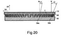
Fig. 19 , the inclined orientation of themicrogrooves diffraction grating 10 from themold 50 and/or to reduce the probability of mold breakage. Theprotrusions 7 of the grating 10 may slide in themicrogrooves - Referring to
Fig. 20 , the relative orientation of themicrogrooves 58 may also be such that a slight expansion of thediffractive lens 60 is required for the separation of thelens 60 from themold 50. The curable material of the lens may be expanded e.g. by heating. Thediffractive lens 60 may be a diverging lens, i.e. it may have a negative focal length. Theprotrusions 7 of the grating 10 may slide in themicrogrooves lens 60 is expanded. - In the cases according to
Fig. 19 and20 , the variation of the inclination angles is gradual, i.e. the difference between the inclination angles ofadjacent microgrooves 58 is very small. - In general, the form and/or divergence and/or direction of a light beam may be modified using a diffractive beam shaping element, said beam shaping element comprising inclined diffractive protrusions.
- Thanks to the reduced probability of mold breakage, the method according to the present invention is especially suitable for mass production of optical diffraction gratings having a low clearance angle.
- The dimensions of the
diffraction gratings 10 and themolds 50 have been exaggerated in theschematic drawings 1 to 10 and 13 to 19.Actual diffraction gratings 10 andmolds 50 may comprise several thousands ofprotrusions 7 andmicrogrooves 58. - For a person skilled in the art, it will be clear that modifications and variations of the devices and the method according to the present invention are perceivable. The particular embodiments described above with reference to the accompanying drawings are illustrative only and not meant to limit the scope of the invention, which is defined by the appended claims.


Claims (15)
- A method of producing a diffraction grating (10) by using a mold (50), which mold (50) has a plurality of adjacent microscopic grooves (58), each groove having a first side and second side forming a first and a second angle with respect to the normal (N) of the mold, the depth (h) of the grooves (58) being greater than or equal to 0.4 times the grating period (d) of the mold (50), said method comprising at least:- applying curable substance (M1) to said mold (50),- curing said substance (M1) at least partially to produce the diffraction grating (10), and- separating said diffraction grating (10) from said mold (50),characterized in that- the inclination (φ) of said grooves (58) being equal to the average of the first and second angles is greater than or equal to 20 degrees and smaller than or equal to 70 degrees with respect to the normal (N) of the plane of the mold (50),- the grating period (d) of said mold (50) is greater than or equal to 0.2 µm and smaller than or equal to 10 µm,- the clearance angle (γ) of said grooves (58) being equal to the differrence of the first and second angles is greater than 0 degrees and smaller than or equal to 20 degrees, and that the method further comprises applying an anti-adhesion layer (30) to said mold (50) to facilitate separation of the diffraction grating (10) from said mold(50).
- The method according to claim 1, wherein the inclination (φ) of said grooves (58) is greater than or equal to 25 degrees and smaller than or equal to 45 degrees with respect to the normal (N) of the plane of the mold (50).
- The method according to claims 1 or 2, wherein the clearance angle (φ) of said grooves (58) is greater than or equal to 5 degrees and smaller than or equal to 12 degrees.
- The method according any of the preceding claims 1 to 3, wherein the filling factor (c2) of the mold (50) is greater than or equal to 0.2 and smaller than or equal to 0.8.
- The method according to any of the preceding claims 1 to 4, wherein the depth (h) of the grooves (58) is greater than or equal to 0.6 times the grating period (d).
- The method according to any of the preceding claims 1 to 5 wherein said substance (M1) is cured by heat.
- The method according to claim 6 wherein said diffraction grating (10) is separated from said mold (50) when the temperature of the substance (M1) of the grating (10) is greater than or equal to 50°C.
- The method according to any of the preceding claims 1 to 5 wherein said substance (M1) is cured by UV radiation.
- The method according to any of the preceding claims 1 to 8 wherein said diffraction grating (10) is separated from said mold (50) when the substance (M1) of the grating (10) is in semi-hardened state.
- The method according to any of the preceding claims 1 to 9 further comprising joining a substrate plate (20) to said diffraction grating (10).
- The method according to claim 10 wherein the diffraction grating (10) is separated from said mold 50 by directing a separating force to the corner and/or edge of said substrate plate (20).
- The method according to claim 10 or 11 wherein said substrate plate (20) is flexible.
- The method according to any of the preceding claims 10 to 12 further comprising treating said substrate plate (20) with an adhesion promoting agent.
- The method according to any of the preceding claims 1 to 13 wherein said mold (50) comprises at least a first groove (58a) having a first inclination (φ1), and a second groove (58b) having a second inclination (φ2), said first inclination (φ1) being different from said second inclination (φ2).
- The method according to any of the preceding claims 1 to 14 wherein at least one area (A3) of the mold (50) comprises curved and/or circular grooves (58).
Applications Claiming Priority (1)
| Application Number | Priority Date | Filing Date | Title |
|---|---|---|---|
| PCT/FI2005/050422WO2007057500A1 (en) | 2005-11-18 | 2005-11-18 | Method of producing a diffraction grating element |
Publications (3)
| Publication Number | Publication Date |
|---|---|
| EP1949147A1 EP1949147A1 (en) | 2008-07-30 |
| EP1949147A4 EP1949147A4 (en) | 2010-07-14 |
| EP1949147B1true EP1949147B1 (en) | 2012-03-21 |
Family
ID=38048321
Family Applications (1)
| Application Number | Title | Priority Date | Filing Date |
|---|---|---|---|
| EP05812973AActiveEP1949147B1 (en) | 2005-11-18 | 2005-11-18 | Method of producing a diffraction grating element |
Country Status (6)
| Country | Link |
|---|---|
| US (1) | US8092723B2 (en) |
| EP (1) | EP1949147B1 (en) |
| JP (1) | JP5266059B2 (en) |
| CN (1) | CN101313234B (en) |
| AT (1) | ATE550685T1 (en) |
| WO (1) | WO2007057500A1 (en) |
Families Citing this family (89)
| Publication number | Priority date | Publication date | Assignee | Title |
|---|---|---|---|---|
| US7885506B2 (en) | 2008-09-26 | 2011-02-08 | Nokia Corporation | Device and a method for polarized illumination of a micro-display |
| JP5380988B2 (en)* | 2008-09-30 | 2014-01-08 | 凸版印刷株式会社 | Optical element |
| CN102460237B (en)* | 2009-06-16 | 2015-04-15 | 皇家飞利浦电子股份有限公司 | Slanted grating and method for producing it |
| NL2003950C2 (en)* | 2009-12-11 | 2011-06-15 | Panalytical Bv | METHOD FOR MANUFACTURING A MULTI-LAYER STRUCTURE WITH A LATERAL PATTERN FOR USE IN THE XUV WAVE LENGTH AREA AND BT AND LMAG STRUCTURES MANUFACTURED BY THIS METHOD. |
| JP5621458B2 (en)* | 2010-09-22 | 2014-11-12 | 三菱瓦斯化学株式会社 | Optical device |
| US9075566B2 (en) | 2012-03-02 | 2015-07-07 | Microsoft Technoogy Licensing, LLC | Flexible hinge spine |
| JP6119102B2 (en)* | 2012-03-02 | 2017-04-26 | 大日本印刷株式会社 | Nanoimprint method |
| US9460029B2 (en) | 2012-03-02 | 2016-10-04 | Microsoft Technology Licensing, Llc | Pressure sensitive keys |
| US20130300590A1 (en) | 2012-05-14 | 2013-11-14 | Paul Henry Dietz | Audio Feedback |
| RU2587072C1 (en) | 2012-06-01 | 2016-06-10 | Топпан Принтинг Ко., Лтд. | Non-isometric reflective display element, data medium using non-isometric reflective display element |
| DE102013107909B4 (en)* | 2013-07-24 | 2015-04-09 | Schott Ag | Method and system for embossing a structure on a substrate coated with a lacquer |
| CN103576220B (en)* | 2013-10-11 | 2016-01-06 | 中国科学院上海光学精密机械研究所 | Quartz 1 × 2 beam splitting skew ray grid of TE polarization |
| US10324733B2 (en) | 2014-07-30 | 2019-06-18 | Microsoft Technology Licensing, Llc | Shutdown notifications |
| US9304235B2 (en) | 2014-07-30 | 2016-04-05 | Microsoft Technology Licensing, Llc | Microfabrication |
| US20160033784A1 (en)* | 2014-07-30 | 2016-02-04 | Tapani Levola | Optical Components |
| US10254942B2 (en) | 2014-07-31 | 2019-04-09 | Microsoft Technology Licensing, Llc | Adaptive sizing and positioning of application windows |
| US9787576B2 (en) | 2014-07-31 | 2017-10-10 | Microsoft Technology Licensing, Llc | Propagating routing awareness for autonomous networks |
| US10678412B2 (en) | 2014-07-31 | 2020-06-09 | Microsoft Technology Licensing, Llc | Dynamic joint dividers for application windows |
| US10592080B2 (en) | 2014-07-31 | 2020-03-17 | Microsoft Technology Licensing, Llc | Assisted presentation of application windows |
| US9535253B2 (en) | 2015-02-09 | 2017-01-03 | Microsoft Technology Licensing, Llc | Display system |
| US11086216B2 (en) | 2015-02-09 | 2021-08-10 | Microsoft Technology Licensing, Llc | Generating electronic components |
| US9429692B1 (en) | 2015-02-09 | 2016-08-30 | Microsoft Technology Licensing, Llc | Optical components |
| US10317677B2 (en) | 2015-02-09 | 2019-06-11 | Microsoft Technology Licensing, Llc | Display system |
| US10018844B2 (en) | 2015-02-09 | 2018-07-10 | Microsoft Technology Licensing, Llc | Wearable image display system |
| US9827209B2 (en) | 2015-02-09 | 2017-11-28 | Microsoft Technology Licensing, Llc | Display system |
| US9423360B1 (en) | 2015-02-09 | 2016-08-23 | Microsoft Technology Licensing, Llc | Optical components |
| US9513480B2 (en) | 2015-02-09 | 2016-12-06 | Microsoft Technology Licensing, Llc | Waveguide |
| US9372347B1 (en) | 2015-02-09 | 2016-06-21 | Microsoft Technology Licensing, Llc | Display system |
| EP3062142B1 (en) | 2015-02-26 | 2018-10-03 | Nokia Technologies OY | Apparatus for a near-eye display |
| EP3745167A1 (en)* | 2015-04-07 | 2020-12-02 | Magic Leap, Inc. | Diffraction grating and method of manufacture |
| US10650552B2 (en) | 2016-12-29 | 2020-05-12 | Magic Leap, Inc. | Systems and methods for augmented reality |
| EP4300160A3 (en) | 2016-12-30 | 2024-05-29 | Magic Leap, Inc. | Polychromatic light out-coupling apparatus, near-eye displays comprising the same, and method of out-coupling polychromatic light |
| US10877192B2 (en) | 2017-04-18 | 2020-12-29 | Saudi Arabian Oil Company | Method of fabricating smart photonic structures for material monitoring |
| RU2659875C1 (en)* | 2017-07-26 | 2018-07-04 | Федеральное государственное бюджетное учреждение науки Физический институт им. П.Н. Лебедева Российской академии наук (ФГБУН ФИАН) | Method for manufacturing the diffraction grating |
| US10578870B2 (en) | 2017-07-26 | 2020-03-03 | Magic Leap, Inc. | Exit pupil expander |
| US11262495B1 (en) | 2017-10-04 | 2022-03-01 | Facebook Technologies, Llc | Waveguides with high refractive index gratings manufactured by post-patterning infusion |
| KR102444339B1 (en)* | 2017-11-21 | 2022-09-19 | 어플라이드 머티어리얼스, 인코포레이티드 | Method of making waveguide couplers |
| KR102562250B1 (en)* | 2017-11-29 | 2023-08-02 | 어플라이드 머티어리얼스, 인코포레이티드 | Method of direct etching fabrication of waveguide combiners |
| KR102858869B1 (en) | 2017-12-10 | 2025-09-11 | 매직 립, 인코포레이티드 | Anti-reflective coatings on optical waveguides |
| CN111712751B (en) | 2017-12-20 | 2022-11-01 | 奇跃公司 | Insert for augmented reality viewing apparatus |
| FI129113B (en)* | 2017-12-22 | 2021-07-15 | Dispelix Oy | Waveguide display and display element with novel grating configuration |
| KR102273970B1 (en)* | 2017-12-26 | 2021-07-07 | 주식회사 엘지화학 | Method for plasma etching process using faraday box |
| US10761330B2 (en)* | 2018-01-23 | 2020-09-01 | Facebook Technologies, Llc | Rainbow reduction in waveguide displays |
| US10914954B2 (en) | 2018-08-03 | 2021-02-09 | Facebook Technologies, Llc | Rainbow reduction for waveguide displays |
| US10845596B2 (en) | 2018-01-23 | 2020-11-24 | Facebook Technologies, Llc | Slanted surface relief grating for rainbow reduction in waveguide display |
| US10818499B2 (en)* | 2018-02-21 | 2020-10-27 | Varian Semiconductor Equipment Associates, Inc. | Optical component having variable depth gratings and method of formation |
| US10755676B2 (en) | 2018-03-15 | 2020-08-25 | Magic Leap, Inc. | Image correction due to deformation of components of a viewing device |
| US11156913B2 (en) | 2018-05-09 | 2021-10-26 | Facebook Technologies, Llc | Nanoimprint lithography process using low surface energy mask |
| US11035988B1 (en)* | 2018-05-22 | 2021-06-15 | Facebook Technologies, Llc | Tunable shrinkage process for manufacturing gratings |
| US10955606B2 (en) | 2018-05-30 | 2021-03-23 | Applied Materials, Inc. | Method of imprinting tilt angle light gratings |
| US10302826B1 (en)* | 2018-05-30 | 2019-05-28 | Applied Materials, Inc. | Controlling etch angles by substrate rotation in angled etch tools |
| US11204491B2 (en) | 2018-05-30 | 2021-12-21 | Magic Leap, Inc. | Compact variable focus configurations |
| JP7319303B2 (en) | 2018-05-31 | 2023-08-01 | マジック リープ, インコーポレイテッド | Radar head pose localization |
| US10825424B2 (en) | 2018-06-05 | 2020-11-03 | Magic Leap, Inc. | Homography transformation matrices based temperature calibration of a viewing system |
| US11092812B2 (en) | 2018-06-08 | 2021-08-17 | Magic Leap, Inc. | Augmented reality viewer with automated surface selection placement and content orientation placement |
| KR102535740B1 (en) | 2018-06-28 | 2023-05-26 | 어플라이드 머티어리얼스, 인코포레이티드 | Fabrication of diffraction gratings |
| US11579441B2 (en) | 2018-07-02 | 2023-02-14 | Magic Leap, Inc. | Pixel intensity modulation using modifying gain values |
| WO2020010226A1 (en) | 2018-07-03 | 2020-01-09 | Magic Leap, Inc. | Systems and methods for virtual and augmented reality |
| US11856479B2 (en) | 2018-07-03 | 2023-12-26 | Magic Leap, Inc. | Systems and methods for virtual and augmented reality along a route with markers |
| CN112585581B (en) | 2018-07-10 | 2024-10-18 | 奇跃公司 | Thread weaving for cross-ISA procedure calls |
| US10795173B2 (en) | 2018-07-13 | 2020-10-06 | Varian Semiconductor Equipment Associates, Inc. | System and method for optimally forming gratings of diffracted optical elements |
| KR102648201B1 (en)* | 2018-07-19 | 2024-03-18 | 어플라이드 머티어리얼스, 인코포레이티드 | Variable Height Slanted Grid Method |
| WO2020023543A1 (en) | 2018-07-24 | 2020-01-30 | Magic Leap, Inc. | Viewing device with dust seal integration |
| CN119197613A (en) | 2018-07-24 | 2024-12-27 | 奇跃公司 | Temperature-dependent calibration of mobile detection equipment |
| WO2020028834A1 (en) | 2018-08-02 | 2020-02-06 | Magic Leap, Inc. | A viewing system with interpupillary distance compensation based on head motion |
| CN116820239A (en) | 2018-08-03 | 2023-09-29 | 奇跃公司 | Fusion gesture based drift correction of fusion gestures for totem in a user interaction system |
| WO2020041615A1 (en) | 2018-08-22 | 2020-02-27 | Magic Leap, Inc. | Patient viewing system |
| EP3881279A4 (en) | 2018-11-16 | 2022-08-17 | Magic Leap, Inc. | Image size triggered clarification to maintain image sharpness |
| US10690821B1 (en)* | 2018-12-14 | 2020-06-23 | Applied Materials, Inc. | Methods of producing slanted gratings |
| US11456152B2 (en)* | 2018-12-17 | 2022-09-27 | Applied Materials, Inc. | Modulation of rolling K vectors of angled gratings |
| CN118409394A (en) | 2018-12-21 | 2024-07-30 | 奇跃公司 | Cavitation structures for promoting total internal reflection in waveguides |
| US11150394B2 (en)* | 2019-01-31 | 2021-10-19 | Facebook Technologies, Llc | Duty cycle range increase for waveguide combiners |
| US11667059B2 (en)* | 2019-01-31 | 2023-06-06 | Meta Platforms Technologies, Llc | Techniques for reducing surface adhesion during demolding in nanoimprint lithography |
| WO2020163603A1 (en) | 2019-02-06 | 2020-08-13 | Magic Leap, Inc. | Target intent-based clock speed determination and adjustment to limit total heat generated by multiple processors |
| JP2022523852A (en) | 2019-03-12 | 2022-04-26 | マジック リープ, インコーポレイテッド | Aligning local content between first and second augmented reality viewers |
| WO2020223636A1 (en) | 2019-05-01 | 2020-11-05 | Magic Leap, Inc. | Content provisioning system and method |
| US11137603B2 (en)* | 2019-06-20 | 2021-10-05 | Facebook Technologies, Llc | Surface-relief grating with patterned refractive index modulation |
| WO2021021670A1 (en) | 2019-07-26 | 2021-02-04 | Magic Leap, Inc. | Systems and methods for augmented reality |
| WO2021029693A1 (en)* | 2019-08-14 | 2021-02-18 | 주식회사 엘지화학 | Diffractive light guide plate and manufacturing method therefor |
| WO2021044121A1 (en)* | 2019-09-06 | 2021-03-11 | Bae Systems Plc | Waveguide and method for fabricating a waveguide master grating tool |
| CN110658575B (en)* | 2019-09-16 | 2021-08-24 | 宁波南大光电材料有限公司 | Manufacturing method of helical-tooth grating plate with high aspect ratio structure and grating plate |
| CN110632690B (en)* | 2019-09-16 | 2021-08-24 | 宁波南大光电材料有限公司 | Manufacturing method of staggered inclined-hole-structure grating plate and grating plate |
| JP7635230B2 (en) | 2019-11-14 | 2025-02-25 | マジック リープ, インコーポレイテッド | Systems and methods for virtual and augmented reality |
| CN114667538A (en) | 2019-11-15 | 2022-06-24 | 奇跃公司 | Viewing system for use in a surgical environment |
| FR3103312B1 (en)* | 2019-11-18 | 2023-01-13 | Commissariat Energie Atomique | Method for manufacturing a microelectronic device having an array of inclined reliefs |
| CN111929985A (en)* | 2020-08-13 | 2020-11-13 | 杭州欧光芯科技有限公司 | Nano-imprinting method of helical grating |
| US11487058B2 (en) | 2020-08-13 | 2022-11-01 | Applied Materials, Inc. | Method for manufacturing optical device structures |
| CN112394436B (en)* | 2020-11-25 | 2021-07-06 | 中国科学院上海光学精密机械研究所 | Asymmetric Structure All-Dielectric Reflective Beam Combining Grating in 1064 nm Band |
| TWI767700B (en)* | 2021-05-13 | 2022-06-11 | 明安國際企業股份有限公司 | Manufacturing method of composite product with negative angle shape |
Family Cites Families (23)
| Publication number | Priority date | Publication date | Assignee | Title |
|---|---|---|---|---|
| US4506949A (en)* | 1983-05-27 | 1985-03-26 | Rca Corporation | Diffractive color separation filter |
| JPS63174302U (en)* | 1986-12-03 | 1988-11-11 | ||
| US4908339A (en)* | 1987-06-01 | 1990-03-13 | Blount David H | Flexible glass |
| US5009484A (en)* | 1989-05-03 | 1991-04-23 | Advanced Environmental Research Group | Diffraction gratings having high efficiencies |
| US5116461A (en)* | 1991-04-22 | 1992-05-26 | Motorola, Inc. | Method for fabricating an angled diffraction grating |
| JP3147481B2 (en) | 1992-04-21 | 2001-03-19 | 松下電器産業株式会社 | Mold for forming glass diffraction grating, method for manufacturing the same, and method for manufacturing glass diffraction grating |
| IT1255205B (en) | 1992-07-03 | 1995-10-20 | ENSIMAGE COMPOSITION FOR POLYPROPYLENE FIBERS | |
| US5561558A (en)* | 1993-10-18 | 1996-10-01 | Matsushita Electric Industrial Co., Ltd. | Diffractive optical device |
| JPH07146405A (en)* | 1993-11-24 | 1995-06-06 | Shimadzu Corp | Replica diffraction grating |
| US5630902A (en)* | 1994-12-30 | 1997-05-20 | Honeywell Inc. | Apparatus for use in high fidelty replication of diffractive optical elements |
| US5728324A (en)* | 1995-01-31 | 1998-03-17 | Digital Optics Corporation | Molding diffractive optical elements |
| US5770124A (en) | 1996-04-30 | 1998-06-23 | Minnesota Mining And Manufacturing Company | Method of making glittering cube-corner retroreflective sheeting |
| JPH1096807A (en) | 1996-09-19 | 1998-04-14 | Dainippon Printing Co Ltd | Holographic optical element and manufacturing method thereof |
| JPH10232306A (en)* | 1997-02-20 | 1998-09-02 | Canon Inc | Method for manufacturing diffractive optical element |
| US6079228A (en) | 1997-07-25 | 2000-06-27 | Minolta Co., Ltd. | Forming method of glass element |
| FR2779534B1 (en)* | 1998-06-09 | 2000-07-07 | Commissariat Energie Atomique | PROCESS FOR MANUFACTURING OPTICAL COMPONENTS BY REPLICATION |
| JP3877444B2 (en) | 1998-09-02 | 2007-02-07 | 富士通株式会社 | Diffraction grating |
| US6873087B1 (en) | 1999-10-29 | 2005-03-29 | Board Of Regents, The University Of Texas System | High precision orientation alignment and gap control stages for imprint lithography processes |
| JP2003011140A (en)* | 2001-07-04 | 2003-01-15 | Canon Inc | Release method and apparatus for diffractive optical element |
| EP1602947A4 (en) | 2003-03-13 | 2007-03-28 | Asahi Glass Co Ltd | Diffraction element and optical device |
| JP2005116069A (en) | 2003-10-08 | 2005-04-28 | Ricoh Co Ltd | Polarizing diffraction grating, optical pickup, optical recording / reproducing apparatus, and magneto-optical recording / reproducing apparatus |
| JP4259332B2 (en) | 2004-01-26 | 2009-04-30 | パナソニック電工株式会社 | Optical element manufacturing method and optical element |
| JP4338558B2 (en) | 2004-03-11 | 2009-10-07 | 三洋電機株式会社 | Optical pickup |
- 2005
- 2005-11-18EPEP05812973Apatent/EP1949147B1/enactiveActive
- 2005-11-18JPJP2008540636Apatent/JP5266059B2/enactiveActive
- 2005-11-18CNCN2005800521065Apatent/CN101313234B/enactiveActive
- 2005-11-18USUS12/094,232patent/US8092723B2/enactiveActive
- 2005-11-18ATAT05812973Tpatent/ATE550685T1/enactive
- 2005-11-18WOPCT/FI2005/050422patent/WO2007057500A1/enactiveApplication Filing
Also Published As
| Publication number | Publication date |
|---|---|
| EP1949147A1 (en) | 2008-07-30 |
| JP5266059B2 (en) | 2013-08-21 |
| US20090224416A1 (en) | 2009-09-10 |
| US8092723B2 (en) | 2012-01-10 |
| ATE550685T1 (en) | 2012-04-15 |
| EP1949147A4 (en) | 2010-07-14 |
| JP2009516225A (en) | 2009-04-16 |
| CN101313234A (en) | 2008-11-26 |
| WO2007057500A1 (en) | 2007-05-24 |
| CN101313234B (en) | 2011-01-05 |
Similar Documents
| Publication | Publication Date | Title |
|---|---|---|
| EP1949147B1 (en) | Method of producing a diffraction grating element | |
| CN100437158C (en) | Manufacturing micro-structured elements | |
| US7113336B2 (en) | Microlens including wire-grid polarizer and methods of manufacture | |
| KR100624414B1 (en) | Method for Manufacturing Diffractive Lens Array Mold and Shock Dispenser | |
| EP0795139A1 (en) | Method for making surface relief profilers | |
| EP2225096B1 (en) | Manufacturing optical elements | |
| KR20090058729A (en) | Hybrid Micro Lens Array and Manufacturing Method Thereof | |
| EP2033050B1 (en) | Manufacturing a replication tool | |
| JP4401139B2 (en) | Pattern forming method and optical element | |
| JP3731017B2 (en) | Optical device manufacturing method | |
| JP6083565B2 (en) | Manufacturing method of fine structure | |
| JP2012252113A (en) | Method for manufacturing wafer lens | |
| KR100930925B1 (en) | Composite Imprint Stamp and Manufacturing Method | |
| WO2005022208A1 (en) | Methacrylic resin cast plate having surface micro structure and method of manufacturing the same | |
| JP2007219006A (en) | Pattern forming method and optical element | |
| JP3619540B2 (en) | Optical device materials, optical devices, and optical device manufacturing methods | |
| JP3165167B2 (en) | Micro lens and manufacturing method thereof | |
| US20250093559A1 (en) | Diffraction grating and mold for forming diffraction grating | |
| JP2003307608A (en) | Method for manufacturing diffractive optical element | |
| KR20220159021A (en) | Manufacturing method of engineering and optics functional surface treatment using two photon polymerization and nanoimprint | |
| KR20220159022A (en) | Treatment manufactured by using two photon polymerization and nanoimprint | |
| HK1086071B (en) | Manufacturing micro-structured elements | |
| JP4212532B2 (en) | Stamper generation method | |
| Rogers et al. | High-fidelity replication of diffractive optics using radiation-curable liquid photopolymers | |
| JP2005326542A (en) | Microlens structure and manufacturing method thereof |
Legal Events
| Date | Code | Title | Description |
|---|---|---|---|
| PUAI | Public reference made under article 153(3) epc to a published international application that has entered the european phase | Free format text:ORIGINAL CODE: 0009012 | |
| 17P | Request for examination filed | Effective date:20080514 | |
| AK | Designated contracting states | Kind code of ref document:A1 Designated state(s):AT BE BG CH CY CZ DE DK EE ES FI FR GB GR HU IE IS IT LI LT LU LV MC NL PL PT RO SE SI SK TR | |
| A4 | Supplementary search report drawn up and despatched | Effective date:20100615 | |
| RIC1 | Information provided on ipc code assigned before grant | Ipc:G03F 7/00 20060101ALI20100609BHEP Ipc:B81C 1/00 20060101ALI20100609BHEP Ipc:G02B 5/18 20060101AFI20070713BHEP | |
| GRAP | Despatch of communication of intention to grant a patent | Free format text:ORIGINAL CODE: EPIDOSNIGR1 | |
| DAX | Request for extension of the european patent (deleted) | ||
| GRAS | Grant fee paid | Free format text:ORIGINAL CODE: EPIDOSNIGR3 | |
| GRAA | (expected) grant | Free format text:ORIGINAL CODE: 0009210 | |
| RAP1 | Party data changed (applicant data changed or rights of an application transferred) | Owner name:NANOCOMP OY LTD. | |
| AK | Designated contracting states | Kind code of ref document:B1 Designated state(s):AT BE BG CH CY CZ DE DK EE ES FI FR GB GR HU IE IS IT LI LT LU LV MC NL PL PT RO SE SI SK TR | |
| REG | Reference to a national code | Ref country code:GB Ref legal event code:FG4D | |
| REG | Reference to a national code | Ref country code:CH Ref legal event code:EP | |
| REG | Reference to a national code | Ref country code:IE Ref legal event code:FG4D | |
| REG | Reference to a national code | Ref country code:AT Ref legal event code:REF Ref document number:550685 Country of ref document:AT Kind code of ref document:T Effective date:20120415 | |
| REG | Reference to a national code | Ref country code:DE Ref legal event code:R096 Ref document number:602005033309 Country of ref document:DE Effective date:20120516 | |
| REG | Reference to a national code | Ref country code:NL Ref legal event code:VDEP Effective date:20120321 | |
| RAP2 | Party data changed (patent owner data changed or rights of a patent transferred) | Owner name:NANOCOMP OY LTD. | |
| PG25 | Lapsed in a contracting state [announced via postgrant information from national office to epo] | Ref country code:LT Free format text:LAPSE BECAUSE OF FAILURE TO SUBMIT A TRANSLATION OF THE DESCRIPTION OR TO PAY THE FEE WITHIN THE PRESCRIBED TIME-LIMIT Effective date:20120321 | |
| REG | Reference to a national code | Ref country code:CH Ref legal event code:PCOW Free format text:NANOCOMP OY LTD.;ENSOLANTIE 6;80710 LEHMO (FI) Ref country code:CH Ref legal event code:NV Representative=s name:BUGNION S.A. | |
| LTIE | Lt: invalidation of european patent or patent extension | Effective date:20120321 | |
| PG25 | Lapsed in a contracting state [announced via postgrant information from national office to epo] | Ref country code:LV Free format text:LAPSE BECAUSE OF FAILURE TO SUBMIT A TRANSLATION OF THE DESCRIPTION OR TO PAY THE FEE WITHIN THE PRESCRIBED TIME-LIMIT Effective date:20120321 Ref country code:FI Free format text:LAPSE BECAUSE OF FAILURE TO SUBMIT A TRANSLATION OF THE DESCRIPTION OR TO PAY THE FEE WITHIN THE PRESCRIBED TIME-LIMIT Effective date:20120321 Ref country code:GR Free format text:LAPSE BECAUSE OF FAILURE TO SUBMIT A TRANSLATION OF THE DESCRIPTION OR TO PAY THE FEE WITHIN THE PRESCRIBED TIME-LIMIT Effective date:20120622 | |
| REG | Reference to a national code | Ref country code:AT Ref legal event code:MK05 Ref document number:550685 Country of ref document:AT Kind code of ref document:T Effective date:20120321 | |
| PG25 | Lapsed in a contracting state [announced via postgrant information from national office to epo] | Ref country code:CY Free format text:LAPSE BECAUSE OF FAILURE TO SUBMIT A TRANSLATION OF THE DESCRIPTION OR TO PAY THE FEE WITHIN THE PRESCRIBED TIME-LIMIT Effective date:20120321 | |
| PG25 | Lapsed in a contracting state [announced via postgrant information from national office to epo] | Ref country code:PL Free format text:LAPSE BECAUSE OF FAILURE TO SUBMIT A TRANSLATION OF THE DESCRIPTION OR TO PAY THE FEE WITHIN THE PRESCRIBED TIME-LIMIT Effective date:20120321 Ref country code:CZ Free format text:LAPSE BECAUSE OF FAILURE TO SUBMIT A TRANSLATION OF THE DESCRIPTION OR TO PAY THE FEE WITHIN THE PRESCRIBED TIME-LIMIT Effective date:20120321 Ref country code:SE Free format text:LAPSE BECAUSE OF FAILURE TO SUBMIT A TRANSLATION OF THE DESCRIPTION OR TO PAY THE FEE WITHIN THE PRESCRIBED TIME-LIMIT Effective date:20120321 Ref country code:SI Free format text:LAPSE BECAUSE OF FAILURE TO SUBMIT A TRANSLATION OF THE DESCRIPTION OR TO PAY THE FEE WITHIN THE PRESCRIBED TIME-LIMIT Effective date:20120321 Ref country code:RO Free format text:LAPSE BECAUSE OF FAILURE TO SUBMIT A TRANSLATION OF THE DESCRIPTION OR TO PAY THE FEE WITHIN THE PRESCRIBED TIME-LIMIT Effective date:20120321 Ref country code:IS Free format text:LAPSE BECAUSE OF FAILURE TO SUBMIT A TRANSLATION OF THE DESCRIPTION OR TO PAY THE FEE WITHIN THE PRESCRIBED TIME-LIMIT Effective date:20120721 Ref country code:BE Free format text:LAPSE BECAUSE OF FAILURE TO SUBMIT A TRANSLATION OF THE DESCRIPTION OR TO PAY THE FEE WITHIN THE PRESCRIBED TIME-LIMIT Effective date:20120321 Ref country code:EE Free format text:LAPSE BECAUSE OF FAILURE TO SUBMIT A TRANSLATION OF THE DESCRIPTION OR TO PAY THE FEE WITHIN THE PRESCRIBED TIME-LIMIT Effective date:20120321 | |
| PG25 | Lapsed in a contracting state [announced via postgrant information from national office to epo] | Ref country code:PT Free format text:LAPSE BECAUSE OF FAILURE TO SUBMIT A TRANSLATION OF THE DESCRIPTION OR TO PAY THE FEE WITHIN THE PRESCRIBED TIME-LIMIT Effective date:20120723 Ref country code:SK Free format text:LAPSE BECAUSE OF FAILURE TO SUBMIT A TRANSLATION OF THE DESCRIPTION OR TO PAY THE FEE WITHIN THE PRESCRIBED TIME-LIMIT Effective date:20120321 | |
| PLBE | No opposition filed within time limit | Free format text:ORIGINAL CODE: 0009261 | |
| STAA | Information on the status of an ep patent application or granted ep patent | Free format text:STATUS: NO OPPOSITION FILED WITHIN TIME LIMIT | |
| PG25 | Lapsed in a contracting state [announced via postgrant information from national office to epo] | Ref country code:DK Free format text:LAPSE BECAUSE OF FAILURE TO SUBMIT A TRANSLATION OF THE DESCRIPTION OR TO PAY THE FEE WITHIN THE PRESCRIBED TIME-LIMIT Effective date:20120321 Ref country code:NL Free format text:LAPSE BECAUSE OF FAILURE TO SUBMIT A TRANSLATION OF THE DESCRIPTION OR TO PAY THE FEE WITHIN THE PRESCRIBED TIME-LIMIT Effective date:20120321 Ref country code:AT Free format text:LAPSE BECAUSE OF FAILURE TO SUBMIT A TRANSLATION OF THE DESCRIPTION OR TO PAY THE FEE WITHIN THE PRESCRIBED TIME-LIMIT Effective date:20120321 | |
| 26N | No opposition filed | Effective date:20130102 | |
| PG25 | Lapsed in a contracting state [announced via postgrant information from national office to epo] | Ref country code:IT Free format text:LAPSE BECAUSE OF FAILURE TO SUBMIT A TRANSLATION OF THE DESCRIPTION OR TO PAY THE FEE WITHIN THE PRESCRIBED TIME-LIMIT Effective date:20120321 | |
| REG | Reference to a national code | Ref country code:DE Ref legal event code:R097 Ref document number:602005033309 Country of ref document:DE Effective date:20130102 | |
| PG25 | Lapsed in a contracting state [announced via postgrant information from national office to epo] | Ref country code:ES Free format text:LAPSE BECAUSE OF FAILURE TO SUBMIT A TRANSLATION OF THE DESCRIPTION OR TO PAY THE FEE WITHIN THE PRESCRIBED TIME-LIMIT Effective date:20120702 | |
| PG25 | Lapsed in a contracting state [announced via postgrant information from national office to epo] | Ref country code:BG Free format text:LAPSE BECAUSE OF FAILURE TO SUBMIT A TRANSLATION OF THE DESCRIPTION OR TO PAY THE FEE WITHIN THE PRESCRIBED TIME-LIMIT Effective date:20120621 | |
| REG | Reference to a national code | Ref country code:IE Ref legal event code:MM4A | |
| PG25 | Lapsed in a contracting state [announced via postgrant information from national office to epo] | Ref country code:IE Free format text:LAPSE BECAUSE OF NON-PAYMENT OF DUE FEES Effective date:20121118 | |
| PG25 | Lapsed in a contracting state [announced via postgrant information from national office to epo] | Ref country code:MC Free format text:LAPSE BECAUSE OF NON-PAYMENT OF DUE FEES Effective date:20121130 Ref country code:TR Free format text:LAPSE BECAUSE OF FAILURE TO SUBMIT A TRANSLATION OF THE DESCRIPTION OR TO PAY THE FEE WITHIN THE PRESCRIBED TIME-LIMIT Effective date:20120321 | |
| PG25 | Lapsed in a contracting state [announced via postgrant information from national office to epo] | Ref country code:LU Free format text:LAPSE BECAUSE OF NON-PAYMENT OF DUE FEES Effective date:20121118 | |
| PG25 | Lapsed in a contracting state [announced via postgrant information from national office to epo] | Ref country code:HU Free format text:LAPSE BECAUSE OF FAILURE TO SUBMIT A TRANSLATION OF THE DESCRIPTION OR TO PAY THE FEE WITHIN THE PRESCRIBED TIME-LIMIT Effective date:20051118 | |
| REG | Reference to a national code | Ref country code:FR Ref legal event code:PLFP Year of fee payment:11 | |
| REG | Reference to a national code | Ref country code:FR Ref legal event code:PLFP Year of fee payment:12 | |
| REG | Reference to a national code | Ref country code:FR Ref legal event code:PLFP Year of fee payment:13 | |
| REG | Reference to a national code | Ref country code:DE Ref legal event code:R082 Ref document number:602005033309 Country of ref document:DE Representative=s name:HGF EUROPE LLP, DE Ref country code:DE Ref legal event code:R081 Ref document number:602005033309 Country of ref document:DE Owner name:RADIANT OPTO-ELECTRONICS CORPORATION, TW Free format text:FORMER OWNER: NANOCOMP OY LTD., JOENSUU, FI | |
| REG | Reference to a national code | Ref country code:GB Ref legal event code:732E Free format text:REGISTERED BETWEEN 20240229 AND 20240306 | |
| PGFP | Annual fee paid to national office [announced via postgrant information from national office to epo] | Ref country code:GB Payment date:20240902 Year of fee payment:20 | |
| PGFP | Annual fee paid to national office [announced via postgrant information from national office to epo] | Ref country code:FR Payment date:20240809 Year of fee payment:20 | |
| PGFP | Annual fee paid to national office [announced via postgrant information from national office to epo] | Ref country code:DE Payment date:20240812 Year of fee payment:20 | |
| PGFP | Annual fee paid to national office [announced via postgrant information from national office to epo] | Ref country code:CH Payment date:20241201 Year of fee payment:20 |