EP1947684B1 - Semiconductor base material and method of manufacturing the material - Google Patents
Semiconductor base material and method of manufacturing the materialDownload PDFInfo
- Publication number
- EP1947684B1 EP1947684B1EP08004987.7AEP08004987AEP1947684B1EP 1947684 B1EP1947684 B1EP 1947684B1EP 08004987 AEP08004987 AEP 08004987AEP 1947684 B1EP1947684 B1EP 1947684B1
- Authority
- EP
- European Patent Office
- Prior art keywords
- growth
- plane
- substrate
- concavo
- convex
- Prior art date
- Legal status (The legal status is an assumption and is not a legal conclusion. Google has not performed a legal analysis and makes no representation as to the accuracy of the status listed.)
- Expired - Lifetime
Links
Images


Classifications
- H—ELECTRICITY
- H01—ELECTRIC ELEMENTS
- H01L—SEMICONDUCTOR DEVICES NOT COVERED BY CLASS H10
- H01L21/00—Processes or apparatus adapted for the manufacture or treatment of semiconductor or solid state devices or of parts thereof
- H01L21/02—Manufacture or treatment of semiconductor devices or of parts thereof
- H01L21/04—Manufacture or treatment of semiconductor devices or of parts thereof the devices having potential barriers, e.g. a PN junction, depletion layer or carrier concentration layer
- H01L21/34—Manufacture or treatment of semiconductor devices or of parts thereof the devices having potential barriers, e.g. a PN junction, depletion layer or carrier concentration layer the devices having semiconductor bodies not provided for in groups H01L21/18, H10D48/04 and H10D48/07, with or without impurities, e.g. doping materials
- C—CHEMISTRY; METALLURGY
- C30—CRYSTAL GROWTH
- C30B—SINGLE-CRYSTAL GROWTH; UNIDIRECTIONAL SOLIDIFICATION OF EUTECTIC MATERIAL OR UNIDIRECTIONAL DEMIXING OF EUTECTOID MATERIAL; REFINING BY ZONE-MELTING OF MATERIAL; PRODUCTION OF A HOMOGENEOUS POLYCRYSTALLINE MATERIAL WITH DEFINED STRUCTURE; SINGLE CRYSTALS OR HOMOGENEOUS POLYCRYSTALLINE MATERIAL WITH DEFINED STRUCTURE; AFTER-TREATMENT OF SINGLE CRYSTALS OR A HOMOGENEOUS POLYCRYSTALLINE MATERIAL WITH DEFINED STRUCTURE; APPARATUS THEREFOR
- C30B29/00—Single crystals or homogeneous polycrystalline material with defined structure characterised by the material or by their shape
- C30B29/10—Inorganic compounds or compositions
- C30B29/40—AIIIBV compounds wherein A is B, Al, Ga, In or Tl and B is N, P, As, Sb or Bi
- C30B29/403—AIII-nitrides
- C—CHEMISTRY; METALLURGY
- C30—CRYSTAL GROWTH
- C30B—SINGLE-CRYSTAL GROWTH; UNIDIRECTIONAL SOLIDIFICATION OF EUTECTIC MATERIAL OR UNIDIRECTIONAL DEMIXING OF EUTECTOID MATERIAL; REFINING BY ZONE-MELTING OF MATERIAL; PRODUCTION OF A HOMOGENEOUS POLYCRYSTALLINE MATERIAL WITH DEFINED STRUCTURE; SINGLE CRYSTALS OR HOMOGENEOUS POLYCRYSTALLINE MATERIAL WITH DEFINED STRUCTURE; AFTER-TREATMENT OF SINGLE CRYSTALS OR A HOMOGENEOUS POLYCRYSTALLINE MATERIAL WITH DEFINED STRUCTURE; APPARATUS THEREFOR
- C30B25/00—Single-crystal growth by chemical reaction of reactive gases, e.g. chemical vapour-deposition growth
- C30B25/02—Epitaxial-layer growth
- C30B25/18—Epitaxial-layer growth characterised by the substrate
- H—ELECTRICITY
- H01—ELECTRIC ELEMENTS
- H01L—SEMICONDUCTOR DEVICES NOT COVERED BY CLASS H10
- H01L21/00—Processes or apparatus adapted for the manufacture or treatment of semiconductor or solid state devices or of parts thereof
- H01L21/02—Manufacture or treatment of semiconductor devices or of parts thereof
- H01L21/02104—Forming layers
- H01L21/02365—Forming inorganic semiconducting materials on a substrate
- H01L21/02367—Substrates
- H01L21/0237—Materials
- H01L21/0242—Crystalline insulating materials
- H—ELECTRICITY
- H01—ELECTRIC ELEMENTS
- H01L—SEMICONDUCTOR DEVICES NOT COVERED BY CLASS H10
- H01L21/00—Processes or apparatus adapted for the manufacture or treatment of semiconductor or solid state devices or of parts thereof
- H01L21/02—Manufacture or treatment of semiconductor devices or of parts thereof
- H01L21/02104—Forming layers
- H01L21/02365—Forming inorganic semiconducting materials on a substrate
- H01L21/02367—Substrates
- H01L21/02433—Crystal orientation
- H—ELECTRICITY
- H01—ELECTRIC ELEMENTS
- H01L—SEMICONDUCTOR DEVICES NOT COVERED BY CLASS H10
- H01L21/00—Processes or apparatus adapted for the manufacture or treatment of semiconductor or solid state devices or of parts thereof
- H01L21/02—Manufacture or treatment of semiconductor devices or of parts thereof
- H01L21/02104—Forming layers
- H01L21/02365—Forming inorganic semiconducting materials on a substrate
- H01L21/02518—Deposited layers
- H01L21/02521—Materials
- H01L21/02538—Group 13/15 materials
- H01L21/0254—Nitrides
- H—ELECTRICITY
- H01—ELECTRIC ELEMENTS
- H01L—SEMICONDUCTOR DEVICES NOT COVERED BY CLASS H10
- H01L21/00—Processes or apparatus adapted for the manufacture or treatment of semiconductor or solid state devices or of parts thereof
- H01L21/02—Manufacture or treatment of semiconductor devices or of parts thereof
- H01L21/02104—Forming layers
- H01L21/02365—Forming inorganic semiconducting materials on a substrate
- H01L21/02612—Formation types
- H01L21/02617—Deposition types
- H01L21/02636—Selective deposition, e.g. simultaneous growth of mono- and non-monocrystalline semiconductor materials
- H01L21/02639—Preparation of substrate for selective deposition
- H01L21/02642—Mask materials other than SiO2 or SiN
- H—ELECTRICITY
- H01—ELECTRIC ELEMENTS
- H01L—SEMICONDUCTOR DEVICES NOT COVERED BY CLASS H10
- H01L21/00—Processes or apparatus adapted for the manufacture or treatment of semiconductor or solid state devices or of parts thereof
- H01L21/02—Manufacture or treatment of semiconductor devices or of parts thereof
- H01L21/02104—Forming layers
- H01L21/02365—Forming inorganic semiconducting materials on a substrate
- H01L21/02612—Formation types
- H01L21/02617—Deposition types
- H01L21/02636—Selective deposition, e.g. simultaneous growth of mono- and non-monocrystalline semiconductor materials
- H01L21/02647—Lateral overgrowth
- H01L21/0265—Pendeoepitaxy
Definitions
- the present inventionrelates to a semiconductor base and a production method thereof. More particularly, this invention relates to a structure useful when using a semiconductor material associated with easy occurrence of dislocation defects and a method thereof.
- a substrate that does not lattice match therewithsuch as sapphire, SiC, Spinel, and recently Si and the like, has been used due to the absence of a substrate that lattice matches with GaN group materials.
- a GaN film producedcontains dislocations of as many as 10 10 points/cm 2 due to the absence of lattice match. While high luminance Light Emitting Diodes, semiconductor lasers and the like have been realized in recent years, reduction of dislocation density has been desired for improved properties.
- FWHMfull width at half-maximum
- SiO 2is generally used as the mask layer material.
- the Si componenttransfers into the crystal growth layer, constituting a problem of autodoping contamination.
- a sapphire substratecan be used as the base substrate and the method thereof is also disclosed (e.g., JP-A-11-191659 ).
- the above-mentioned methodrequires steps of crystal growing a buffer layer material and a GaN group material on a sapphire base substrate, taking the substrate out from a growth furnace to apply a groove inconvenience of complicated production process, increased number of steps, higher cost and the like.
- the inventionaims at resolving the problem of unattainable selective growth of AlGaN, which has been conventionally difficult. Moreover, the invention aims at avoiding the issue of heat caused by the formation of cavity parts.
- the semiconductor base of the present inventionconsists of a substrate and a semiconductor crystal formed on the substrate by vapor phase growth, wherein the crystal growth plane of the aforementioned substrate is a concavo-convex surface and the aforementioned semiconductor crystal is grown from the concave part and/or the convex part while forming a facet structure, as defined in the appended claims.
- the above-mentioned semiconductor crystalis InGaAlN.
- the convex part of the crystal growth plane of the above-mentioned substratea convex part having a parallel stripe pattern. It is more preferable that the above-mentioned semiconductor crystal be InGaAlN and the longitudinal direction of the stripe be parallel to the (1-100) plane or the (11-20) plane of the InGaAlN crystal.
- the longitudinal direction of the stripebe parallel with the (1-100) plane or the (11-20) plane of the above-mentioned InGaAlN crystal and the precision thereof be not more than 1°.
- the total (A+B) of width A of the convex part and width B of the adjacent concave partis not more than 20 ⁇ m, and a depth H of the aforementioned concave part is not less than 20% of the greater width of A or B.
- 1is a substrate
- 11is a convex part
- 12is a concave part
- 13is a cavity part
- 2is a semiconductor layer.
- the present inventionis characterized in that a concavo-convex surface is formed on a substrate before formation of even a buffer layer and the like, thereby to provide a base surface, on which a facet plane can be formed, from the start of crystal growth. That is, by equipping a concavo-convex surface on the substrate, each or both of the concave plane and the convex plane separated by steps is/are prepared as unit standard surface on which to grow a facet structure in vapor phase growth.
- both the concave plane and the convex planeare prepared as planes capable of facet structure growth
- the crystal growthoccurs in the entirety of the substrate surface in the initial stage of the growth, thus resulting in the growth comprising a facet plane on both the convex part and the concave part.
- the facet structure growthoccurs from either the convex part or the concave part. In some cases, the facet part but non-facet structure growth occurs from the other plane.
- the dislocation line extending from the substrate in the C axis directionis bent toward the lateral direction in the facet plane and fails to propagate upward.
- Subsequent continuous growthmakes the growth plane flat in time and the vicinity of the surface thereof becomes a low dislocation density area due to the absence of propagation of dislocation from the substrate.
- the formation of a low dislocation density areais achieved without using a mask layer as in conventional cases and without necessitating a grounding layer.
- the problem of heat dissipationcan be avoided due to the absence of the need to form a cavity part.
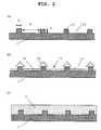
- Figures 1(a) to 1(c)show cross sectional views to explain the state of crystal growth of the semiconductor base not according to the present invention.
- 1is a substrate and 2 is a semiconductor crystal grown by vapor phase growth on the substrate 1.
- On the crystal growth plane of the substrate 1are formed a convex part 11 and a concave part 12, which are the base surfaces on which to form a facet plane from the aforementioned convex part 11 and/or concave part 12.
- the above-mentioned substrate 1is a base substrate on which to grow various semiconductor crystal layers, in the state before the formation of a buffer layer and the like for lattice matching.
- substratesapphire (C-plane, A-plane, R-plane), SiC (6H, 4H, 3C), GaN, AlN, Si, Spinel, ZnO, GaAs, NGO and the like can be used, but other materials may be used.
- the plane,direction of the substrateis not particularly limited and may be a just substrate or one having an off angle.
- Al x Ga 1-x-v In v N(0 ⁇ x ⁇ 1, 0 ⁇ y ⁇ 1, 0 ⁇ x+y ⁇ 1) wherein the composition ratios of x and y are varied, such as GaN, Al 0.2 Ga 0.8 N , In 0.4 Ga 0.6 N and the like is used.
- the conventional mask methodposes a problem of growth on an SiO 2 mask layer. Because the present invention resolves this problem by eliminating masking, conventionally unattainable AlGaN low dislocation density can be now achieved, whereby a low dislocation, high quality film growth is afforded from right above the substrate. As a result, light absorption by GaN layer, a problem in ultraviolet light emitting element and the like, is obliterated, which is particularly preferable from a practical aspect.
- a high temperature GaN filmis grown on a sapphire C-plane substrate via a low temperature buffer layer by conventional MOVPE method and the like.
- the buffer layerbecomes a core, which core joins along with the growth in the lateral direction and becomes flat.
- the sapphire substrateis free of processing, the growth proceeds to form a stable C-plane and GaN becomes flat. This is attributable to the fact that the growth rate in the lateral direction is faster than that of the stable C-plane.
- the growth plane of the substrateis subjected to a concavo-convex processing to suppress the above-mentioned growth in the lateral direction.
- the shape of the concavo-convexis subject to no particular limitation as long as the above-mentioned effect can be achieved, and various shapes can be employed.
- island type intersperse convex partsFor forming such a concavo-convex surface, island type intersperse convex parts, stripe type convex parts consisting of convex lines, lattice convex parts, convex parts wherein the lines forming these are curves and the like, can be employed.
- the convex partone comprising a stripe convex line is preferable, because the production steps thereof can be simplified and regular patterns can be easily formed.
- the longitudinal direction of the stripemay be any, when the material to be grown on the substrate is GaN and said direction is the ⁇ 11-20> direction of the GaN group material, the growth in the lateral direction can be suppressed and oblique ⁇ 1-101 ⁇ facets and the like are easily formed.
- the dislocation propagated in the C axis direction from the substrate sideis bent in this facet plane to the lateral direction and resists upward propagation, which in turn particularly preferably forms a low dislocation density area.
- the direction of the stripe formed by concavo-convex processing of the above-mentioned substrateis most preferably the ⁇ 1-100> direction or the ⁇ 11-20> direction of the InGaAlN crystal.
- the directionmay not match strictly the aforementioned direction. While the presence of a little direction error is tolerable, it is desirable to make the precision of the stripe direction of not more than 1°, particularly preferably within 0.2°, relative to the ⁇ 1-100> direction or the ⁇ 11-20> direction of InGaAIN crystal.
- Fig. 1As shown in (a), substrate 1 wherein width B of a concave part 12 and width A of the convex part 11 are the same, is used. In this case, the growth proceeds while forming facet planes in both the convex part 11 and the concave part 12, thereby forming crystal units 20 and 21. Because, in concave part 12, the growth occurs in the valley between the sidewall and the facet plane, as shown in Fig. 1(b) , a buried valley is included. When the crystal growth continues in this situation, the crystal unit 20 on the convex part 11 and the crystal unit 21 on the concave part grow, films are joined and the concavo-convex surface of substrate 1 is covered as shown in Fig. 1(c) . In this case, a low dislocation area is formed on the upper part where a facet plane was once formed, and the produced film comes to have high quality.
- a substrate 1 wherein width A of convex part 11 is narrower than width B of concave partis used.
- the growthproceeds in the convex part 11 forming a facet plane, and crystal growth occurs in the concave part 12 as well ( Fig. 2(b) ).
- the films grown from the convex part 11 and the concave part 12are joined to cover the concavo-convex surface, as shown in Fig. 2(c) .
- a facet planeWhile the area where a facet plane is formed varies greatly by the combination of width B of the concave part and width A of the convex part, propagation of dislocation can be bent by the formation of facet planes, whereby low dislocation density can be achieved. Accordingly, while this facet plane may be any as long as the propagation of dislocation is bent, in a preferable embodiment as shown in Fig. 1 , crystal unit 20 grown from one facet structure growth base plane does not have a flat part on its top plane but has an angle shape where both facet planes completely cross at the top part ( Fig. 4 shows complete formation of facet and Fig. 5 shows cross sectional photograph showing an incomplete case). Such facet plane shown in Fig. 1 ( Fig.
- Fig. 6is a cross sectional photograph showing such state, wherein it is clearly observed that the dislocation line (black line in the photograph) is bent along the facet growth.
- the area where the facet plane is formedcan be controlled by not only the combination of width but by changing the depth h of the concave part (height of convex part).
- the combination of concavo-convexincludes various ones.
- the width of concave part 12 and convex part 11, and the depth h of the concave partare preferably such that the total (A+B) of width A of the convex part and width B of the adjacent concave part is not more than 20 ⁇ m, and the depth h of the aforementioned concave part is not less than 20% of the greater width of A or B.
- the height necessary for complete formation of the facet in this caseis ⁇ /3/2 (i.e., (square root of 3)/2) relative to the width of the bottom surface.
- Ashould have the height of B ⁇ ⁇ 3/2.
- a or Bexceeds 20 ⁇ m, the necessary height is about 17 ⁇ m, frequently posing the problems of occurrence of warp due to a thick substrate, long time for growth and the like.
- the depth h of the concave parthas been also considered in the same manner as above, and it has been confirmed that when it is set for not less than 20% of the longer of A or B, the facets are formed and reduction of dislocation can be promoted.
- the angle formed by the rising slope of a convex part 11 formed by concavo-convex processing of the substrate, and a substrate planeis preferably not smaller than 60°, particularly desirably as near as possible to a right angle.
- 60°the growth begins from the slope of the convex part and a problem of difficult flattening after facet growth occurred.
- an angle of not less than 60°, among others a rising slope near a right anglepermits formation of facets and flattening thereafter is not substantially inhibited. If possible, a slope angle exceeding 90° is also preferable.
- concave part 12concavo-convex processed on the substrate.
- the growthcan be controlled such that the growth from the concave part 12 becomes slow and the growth from the convex part 11 is dominant.
- Fig. 3shows another embodiment not according to the present invention.
- the formation of concavo-convex and the likeare as shown in Fig. 1 , but as shown in Fig. 3(a) , in this embodiment, a mask layer 3 is formed on the concave part 12 of the substrate 1, which prevents substantial crystal grow from the surface.
- the growth while forming a facet planeoccurs only from the convex part 11, crystal unit 20 is formed ( Fig. 3(b) ), and when the crystal growth is continued, crystal units 20 grown from each convex part 11 are joined to cover the concavo-convex surface as shown in Fig. 3(c) .
- the facet planeis formed, the propagation of dislocation can be bent, thereby low dislocation density can be achieved.
- the mask layer 3an SiO 2 mask and the like can be used as the mask layer 3.
- the processingis free of any particular limitation as long as it prevents substantial crystal growth, such as formation of a thin film and the like.
- the concave part or the convex parta concave part having a minute opening or a convex part having a minute width that cannot cause substantial crystal growth, the growth of the facet structure can be made to occur from only one of them.
- a convex partcan be formed by a conventional photolithography technique, which comprises patterning according to the shape of the convex part and applying etching processing by RIE technique and the like.
- HVPE, MOVPE, MBE and the likemay be method is preferable, but when a thin film is to be prepared, MOVPE method and MBE method are preferable.
- Formation of the facet planecan be controlled by the growth conditions (kind of gas, growth pressure, growth temperature and the like) for crystal growth.
- the growth conditionskind of gas, growth pressure, growth temperature and the like
- lower NH 3 partial pressureleads to easy formation of facets in the ⁇ 1-101> plane and growth at normal pressure leads to easy formation of facet planes as compared to reduced pressure.
- the growth temperatureWhen the growth temperature is raised, the growth in the lateral direction is promoted, and the growth at a low temperature causes more rapid growth in the C axis direction than growth in the lateral direction, thereby making facet plane easy to form.
- the growth conditionsare preferably changed to promote growth in the lateral direction to flatten GaN.
- the growth conditions under which the facet plane is difficult to be formedcan be employed, conversely from the aforementioned.
- a photoresist patterning(width: 2 ⁇ m, period: 4 ⁇ m, stripe direction: stripe extending direction is the ⁇ 1-100> direction of the sapphire substrate) was made on a C-plane sapphire substrate and etched to a 2 ⁇ m depth in a square cross section with an RIE (Reactive Ion Etching) apparatus. The aspect ratio then was 1. After removing the photoresist, the substrate was set on a MOVPE apparatus. Then, the temperature was raised to 1100°C under a hydrogen atmosphere and thermal etching was conducted.
- RIEReactive Ion Etching
- TMGtrimethyl gallium
- the carrier density of the obtained filmwas determined by Hall measurement. Furthermore, a full width at half-maximum of X-ray rocking curve was also measured.
- the carrier densitywas of the same level as general GaN growth.
- the FWHM of XRCwas 107 sec, which was the smallest, and the film had high quality by general evaluation.
- Example 1The procedure followed Example 1 except the shape of the concavo-convex part was changed to the following:. (width: 2 ⁇ m, period: 6 ⁇ m, stripe direction: ⁇ 1-100> of sapphire substrate), and etched to the depth of 0.5 ⁇ m by RIE apparatus in a square cross section.
- Example 1Observation of cross section after growth revealed a flattened film in which the concavo-convex part had been buried as in Example 1; which is shown in Fig. 2(c) .
- Fig. 2(c)For observation of dislocation density, pits were formed and the number thereof was counted in the same manner as in Example 1.
- Example 1Example 1 to grow GaN except an SiO 2 mask was formed on the concave part. Observation of cross section of the film after growth corresponding to 2 ⁇ m revealed GaN grown with a facet plane formed on the upper part of the convex part, as shown in Fig. 3(b) . However, no film was formed in the concave part.
- An n-type AlGaN cladding layer, an InGaN light emitting layer, a p-type AlGaN cladding layer and a p-type GaN contact layerwere successively formed on the film obtained in Example 1 to give an ultraviolet LED wafer having a light emitting wavelength of 370 nm.
- the sample prepared according to the present inventionshowed higher output as compared to the conventional example, and it was found that a high quality LED with less leak current could be prepared.
- Example 1The procedure followed Example 1 except that trimethyl aluminum (TMA) was added when growing a semiconductor layer.
- TMAtrimethyl aluminum
- AlGaNAl composition 0.2
- a photoresist patterning(width: 2 ⁇ m, period: 4 ⁇ m, stripe direction: ⁇ 11-20> of GaN substrate) was made on a GaN substrate and etched to a 2 ⁇ m depth in a square cross section with an RIE apparatus. After removing the photoresist, the substrate was set on a MOVPE apparatus. Then, the temperature was raised to 1000°C under a nitrogen, hydrogen, ammonia mixture atmosphere. Thereafter, TMG - ammonia as a starting material and silane as a dopant were flown to grow an n-type GaN layer. The growth time then corresponded to 4 ⁇ m of conventional GaN growth free of concavo-convex.
- a second crystalwas grown thereon.
- a photoresist patterning(width: 2 ⁇ m, period: 4 ⁇ m, stripe direction: ⁇ 11-20> of GaN substrate) was made on the first GaN crystal and etched to a 2 ⁇ m depth in a square cross section with an RIE apparatus. The patterning was conducted such that the concave part of the first crystal was disposed on the convex part of the substrate. After removing the photoresist, the substrate was set on a MOVPE apparatus. Then, the temperature was raised to 1000°C under a nitrogen, hydrogen, ammonia mixture atmosphere.
- TMG - ammonia as a starting material and silane as a dopantwere flown to grow an n-type GaN layer.
- the growth timethen corresponded to 4 ⁇ m of conventional GaN growth free of concavo-convex.
- a base surface capable of forming a facet planecan be formed from the start of the crystal growth, without using a mask layer, by applying a concavo-convex processing to the substrate.
Landscapes
- Engineering & Computer Science (AREA)
- Chemical & Material Sciences (AREA)
- Manufacturing & Machinery (AREA)
- General Physics & Mathematics (AREA)
- Physics & Mathematics (AREA)
- Computer Hardware Design (AREA)
- Microelectronics & Electronic Packaging (AREA)
- Power Engineering (AREA)
- Condensed Matter Physics & Semiconductors (AREA)
- Materials Engineering (AREA)
- Crystallography & Structural Chemistry (AREA)
- Metallurgy (AREA)
- Organic Chemistry (AREA)
- Inorganic Chemistry (AREA)
- Chemical Kinetics & Catalysis (AREA)
- General Chemical & Material Sciences (AREA)
- Led Devices (AREA)
- Crystals, And After-Treatments Of Crystals (AREA)
- Semiconductor Lasers (AREA)
Description
- The present invention relates to a semiconductor base and a production method thereof. More particularly, this invention relates to a structure useful when using a semiconductor material associated with easy occurrence of dislocation defects and a method thereof.
- For crystal growth of a GaN group material, a substrate that does not lattice match therewith, such as sapphire, SiC, Spinel, and recently Si and the like, has been used due to the absence of a substrate that lattice matches with GaN group materials. However, a GaN film produced contains dislocations of as many as 1010 points/cm2 due to the absence of lattice match. While high luminance Light Emitting Diodes, semiconductor lasers and the like have been realized in recent years, reduction of dislocation density has been desired for improved properties.
- As a method for reducing the dislocation density when, for example, a GaN group semiconductor substrate and the like are grown on a buffer layer and a GaN substrate by vapor phase growth, a method comprising formation of a partial mask on the aforementioned substrate and selective growth to achieve crystal growth in the lateral direction has been proposed, thereby to give a high quality crystal having a reduced dislocation density (e.g.,
JP-A-10-312971 - It has been clarified that, according to the above-mentioned method, a problem occurs that, in the part of a mask layer where growth in the lateral direction occurred, the C axis tilts in a slight amount toward the direction of the lateral growth, which in turn causes a new problem of degraded crystal quality (Abstracts G3.1 of MRS 1998 Fall Meeting). This can be confirmed through measurement (φ scan) of the incident orientation dependency in X-ray rocking curve measurement (XRC). That is, a full width at half-maximum (FWHM) of X-ray rocking curve by incident X-ray from the direction of lateral growth is greater than the FWHM value by X-ray from a stripe direction of a mask layer, which means the presence of orientation dependency in the micro tilting of the C axis. This suggests a possibility of inducing a number of new defects in the junction part of the lateral growth on the mask.
- As the mask layer material, SiO2 is generally used. However, a problem has been found that, when a crystal growth layer is laminated thereon, the Si component transfers into the crystal growth layer, constituting a problem of autodoping contamination.
- When a semiconductor material containing Al, such as AlGaN, is grown on a substrate having an SiO2 mask layer, crystal growth occurs on the mask layer, too, preventing effective selective growth itself.
- In an attempt to solve such problems, a method has been proposed wherein a stripe groove processing is applied to a substrate having a buffer layer and a GaN layer formed on an SiC base substrate, which groove reaching the SiC layer to form a convex, and crystal growth is started from the GaN layer on the top of this convex (Abstracts G3.38 of MRS 1998 Fall Meeting). According to this method, a selective growth without an SiO2 mask layer is possible, whereby resolving various problems caused by the use of the aforementioned SiO2 mask.
- For the above-mentioned method, a sapphire substrate can be used as the base substrate and the method thereof is also disclosed (e.g.,
JP-A-11-191659 - In addition, a method for suppressing propagation of dislocation by forming concavo-convex grooves on a substrate and growing a gallium nitride group semiconductor while forming a cavity in the concave part has been disclosed (
JP-A-2000-106455 - In view of the above-mentioned problems, it is therefore an object of the present invention to avoid various problems caused by the use of a mask layer, and to simplify the production step. The invention additionally aims at resolving the problem of unattainable selective growth of AlGaN, which has been conventionally difficult. Moreover, the invention aims at avoiding the issue of heat caused by the formation of cavity parts.
- The semiconductor base of the present invention consists of a substrate and a semiconductor crystal formed on the substrate by vapor phase growth, wherein the crystal growth plane of the aforementioned substrate is a concavo-convex surface and the aforementioned semiconductor crystal is grown from the concave part and/or the convex part while forming a facet structure, as defined in the appended claims.
- The above-mentioned semiconductor crystal is InGaAlN.
- It is preferable to make the convex part of the crystal growth plane of the above-mentioned substrate a convex part having a parallel stripe pattern. It is more preferable that the above-mentioned semiconductor crystal be InGaAlN and the longitudinal direction of the stripe be parallel to the (1-100) plane or the (11-20) plane of the InGaAlN crystal.
- In a stripe structure obtained by subjecting the above-mentioned substrate to concavo-convex processing, it is desirable that the longitudinal direction of the stripe be parallel with the (1-100) plane or the (11-20) plane of the above-mentioned InGaAlN crystal and the precision thereof be not more than 1°. In a preferable stripe structure, the total (A+B) of width A of the convex part and width B of the adjacent concave part is not more than 20 µm, and a depth H of the aforementioned concave part is not less than 20% of the greater width of A or B.
- It is also desirable to make an angle formed by the rising slope of a convex part formed by concavo-convex processing of the above-mentioned substrate, and a substrate plane to be not smaller than 60°. It is also possible to equip a curved part on the bottom of the concave part.
Figure 1 is a cross section for explanation of the state of crystal growth of the semiconductor base not according to the present invention.Figure 2 is a cross section for explanation of the state of crystal growth of the semiconductor base not according to the presentFigure 3 is a cross section for explanation of the state of crystal growth of the semiconductor base not according to the present invention.Figure 4 is a cross sectional photograph showing complete formation of facets.Figure 5 is a cross sectional photograph showing incomplete formation of facets.Figure 6 is a cross sectional photograph showing bending of the dislocation line (black line in the photograph) along with the growth of the facet.- In each of the
Figures, 1 is a substrate, 11 is a convex part, 12 is a concave part, 13 is a cavity part and 2 is a semiconductor layer. - The present invention is characterized in that a concavo-convex surface is formed on a substrate before formation of even a buffer layer and the like, thereby to provide a base surface, on which a facet plane can be formed, from the start of crystal growth. That is, by equipping a concavo-convex surface on the substrate, each or both of the concave plane and the convex plane separated by steps is/are prepared as unit standard surface on which to grow a facet structure in vapor phase growth. When both the concave plane and the convex plane are prepared as planes capable of facet structure growth, the crystal growth occurs in the entirety of the substrate surface in the initial stage of the growth, thus resulting in the growth comprising a facet plane on both the convex part and the concave part. In contrast, when either the concave plane or the convex plane is substantially incapable of crystal growth because it has an extremely small width and the like, or the crystal growth itself is possible but the surface thereof is processed and substantially incapable of crystal growth, the facet structure growth occurs from either the convex part or the concave part. In some cases, the facet part but non-facet structure growth occurs from the other plane.
- As a result, the dislocation line extending from the substrate in the C axis direction is bent toward the lateral direction in the facet plane and fails to propagate upward. Subsequent continuous growth makes the growth plane flat in time and the vicinity of the surface thereof becomes a low dislocation density area due to the absence of propagation of dislocation from the substrate. In other words, the formation of a low dislocation density area is achieved without using a mask layer as in conventional cases and without necessitating a grounding layer. Particularly, the problem of heat dissipation can be avoided due to the absence of the need to form a cavity part.
- The embodiment of the present invention is explained in detail in the following based on drawings.
Figures 1(a) to 1(c) show cross sectional views to explain the state of crystal growth of the semiconductor base not according to the present invention. In theseFigures, 1 is a substrate and 2 is a semiconductor crystal grown by vapor phase growth on thesubstrate 1. On the crystal growth plane of thesubstrate 1 are formed aconvex part 11 and aconcave part 12, which are the base surfaces on which to form a facet plane from theaforementioned convex part 11 and/orconcave part 12.- The above-mentioned
substrate 1 is a base substrate on which to grow various semiconductor crystal layers, in the state before the formation of a buffer layer and the like for lattice matching. As such substrate, sapphire (C-plane, A-plane, R-plane), SiC (6H, 4H, 3C), GaN, AlN, Si, Spinel, ZnO, GaAs, NGO and the like can be used, but other materials may be used. The plane,direction of the substrate is not particularly limited and may be a just substrate or one having an off angle. In addition, a sapphire substrate and the like having several µm used. - As the semiconductor layer to be grown on the
substrate 1, AlxGa1-x-vInvN (0≤x≤1, 0≤y≤1, 0≤x+y≤1) wherein the composition ratios of x and y are varied, such as GaN, Al0.2Ga0.8N, In0.4Ga0.6N and the like is used. - In the case of a semiconductor material containing Al, such as AlGaN and the like, the conventional mask method poses a problem of growth on an SiO2 mask layer. Because the present invention resolves this problem by eliminating masking, conventionally unattainable AlGaN low dislocation density can be now achieved, whereby a low dislocation, high quality film growth is afforded from right above the substrate. As a result, light absorption by GaN layer, a problem in ultraviolet light emitting element and the like, is obliterated, which is particularly preferable from a practical aspect.
- The following explains a base surface capable of forming a facet plane, wherein concavo-convex shaped
parts substrate 1. - For typical growth of GaN, a high temperature GaN film is grown on a sapphire C-plane substrate via a low temperature buffer layer by conventional MOVPE method and the like. When a high temperature GaN is grown on a low temperature buffer layer, the buffer layer becomes a core, which core joins along with the growth in the lateral direction and becomes flat. At this point, because the sapphire substrate is free of processing, the growth proceeds to form a stable C-plane and GaN becomes flat. This is attributable to the fact that the growth rate in the lateral direction is faster than that of the stable C-plane.
- On the other hand, when the rate of growth in the lateral direction is suppressed and the rate of growth in the C axis direction is increased, an inclined facet {1-101} and the like can be formed. In the present invention, the growth plane of the substrate is subjected to a concavo-convex processing to suppress the above-mentioned growth in the lateral direction.
- In the present invention, the shape of the concavo-convex is subject to no particular limitation as long as the above-mentioned effect can be achieved, and various shapes can be employed.
- For forming such a concavo-convex surface, island type intersperse convex parts, stripe type convex parts consisting of convex lines, lattice convex parts, convex parts wherein the lines forming these are curves and the like, can be employed.
- Of these modes of the convex part, one comprising a stripe convex line is preferable, because the production steps thereof can be simplified and regular patterns can be easily formed. While the longitudinal direction of the stripe may be any, when the material to be grown on the substrate is GaN and said direction is the <11-20> direction of the GaN group material, the growth in the lateral direction can be suppressed and oblique {1-101} facets and the like are easily formed. As a result, the dislocation propagated in the C axis direction from the substrate side is bent in this facet plane to the lateral direction and resists upward propagation, which in turn particularly preferably forms a low dislocation density area.
- Even when the stripe direction is set for the <1-100> direction, similar effects as mentioned above can be obtained by determining the growth conditions permitting easy formation of facet plane.
- The direction of the stripe formed by concavo-convex processing of the above-mentioned substrate is most preferably the <1-100> direction or the <11-20> direction of the InGaAlN crystal. However, because it accompanies a growth phenomenon where adjacent facets are joined and leveled, the direction may not match strictly the aforementioned direction. While the presence of a little direction error is tolerable, it is desirable to make the precision of the stripe direction of not more than 1°, particularly preferably within 0.2°, relative to the <1-100> direction or the <11-20> direction of InGaAIN crystal.
- In
Fig. 1 , as shown in (a),substrate 1 wherein width B of aconcave part 12 and width A of theconvex part 11 are the same, is used. In this case, the growth proceeds while forming facet planes in both theconvex part 11 and theconcave part 12, thereby formingcrystal units concave part 12, the growth occurs in the valley between the sidewall and the facet plane, as shown inFig. 1(b) , a buried valley is included. When the crystal growth continues in this situation, thecrystal unit 20 on theconvex part 11 and thecrystal unit 21 on the concave part grow, films are joined and the concavo-convex surface ofsubstrate 1 is covered as shown inFig. 1(c) . In this case, a low dislocation area is formed on the upper part where a facet plane was once formed, and the produced film comes to have high quality. - In the embodiment of
Fig. 2 , as shown in (a), asubstrate 1 wherein width A ofconvex part 11 is narrower than width B of concave part is used. In this case, the growth proceeds in theconvex part 11 forming a facet plane, and crystal growth occurs in theconcave part 12 as well (Fig. 2(b) ). In this situation, when the crystal growth continues, the films grown from theconvex part 11 and theconcave part 12 are joined to cover the concavo-convex surface, as shown inFig. 2(c) . In this case, while a low dislocation area is formed on theupper part 11 where a facet plane was once formed, but a facet plane is difficult to form from the shape of theconcave part 12, and the effect of bending the dislocation to the lateral direction reduces. Thus, as compared to the embodiment ofFig. 1 , while the effect of reduction of dislocation density is small, the produced film comes to have high quality. - While the area where a facet plane is formed varies greatly by the combination of width B of the concave part and width A of the convex part, propagation of dislocation can be bent by the formation of facet planes, whereby low dislocation density can be achieved. Accordingly, while this facet plane may be any as long as the propagation of dislocation is bent, in a preferable embodiment as shown in
Fig. 1 ,crystal unit 20 grown from one facet structure growth base plane does not have a flat part on its top plane but has an angle shape where both facet planes completely cross at the top part (Fig. 4 shows complete formation of facet andFig. 5 shows cross sectional photograph showing an incomplete case). Such facet plane shown inFig. 1 (Fig. 4 ) is preferable because it can bend almost all the dislocation lines succeeded from the aforementioned base plane and can further reduce the dislocation density right above.Fig. 6 is a cross sectional photograph showing such state, wherein it is clearly observed that the dislocation line (black line in the photograph) is bent along the facet growth. - The area where the facet plane is formed can be controlled by not only the combination of width but by changing the depth h of the concave part (height of convex part).
- As mentioned above, the combination of concavo-convex includes various ones. In view of the application to a light emitting element, the width of
concave part 12 andconvex part 11, and the depth h of the concave part are preferably such that the total (A+B) of width A of the convex part and width B of the adjacent concave part is not more than 20 µm, and the depth h of the aforementioned concave part is not less than 20% of the greater width of A or B. - When the facet plane to be formed is {1-101} facet, the angle of the,facet plane thereof with the substrate plane is about 60°. Therefore, the height necessary for complete formation of the facet in this case is √/3/2 (i.e., (square root of 3)/2) relative to the width of the bottom surface. When the bottom surface is considered to correspond to width B of concave part or width A of convex part, forming the facets, A should have the height of B × √3/2. When A or B exceeds 20 µm, the necessary height is about 17 µm, frequently posing the problems of occurrence of warp due to a thick substrate, long time for growth and the like. As a result of the studies of the present inventors, when A+B≤20 µm, occurrence of warp could be reduced and the growth did not require a long time.
- The depth h of the concave part has been also considered in the same manner as above, and it has been confirmed that when it is set for not less than 20% of the longer of A or B, the facets are formed and reduction of dislocation can be promoted.
- The angle formed by the rising slope of a
convex part 11 formed by concavo-convex processing of the substrate, and a substrate plane is preferably not smaller than 60°, particularly desirably as near as possible to a right angle. When it is smaller than 60°, the growth begins from the slope of the convex part and a problem of difficult flattening after facet growth occurred. As a result of the studies of the present inventors, it has been found that an angle of not less than 60°, among others a rising slope near a right angle, permits formation of facets and flattening thereafter is not substantially inhibited. If possible, a slope angle exceeding 90° is also preferable. - It is also possible to provide a curve on the bottom surface of
concave part 12 concavo-convex processed on the substrate. Typically, a curve having a gentle concave surface when seen at a cross section between the rising base of oneconvex part 11 and the rising base of the adjacentconvex part 11. When such curve is provided, the growth can be controlled such that the growth from theconcave part 12 becomes slow and the growth from theconvex part 11 is dominant. Fig. 3 shows another embodiment not according to the present invention. The formation of concavo-convex and the like are as shown inFig. 1 , but as shown inFig. 3(a) , in this embodiment, amask layer 3 is formed on theconcave part 12 of thesubstrate 1, which prevents substantial crystal grow from the surface. In this case, the growth while forming a facet plane occurs only from theconvex part 11,crystal unit 20 is formed (Fig. 3(b) ), and when the crystal growth is continued,crystal units 20 grown from eachconvex part 11 are joined to cover the concavo-convex surface as shown inFig. 3(c) . In this embodiment, too, when the facet plane is formed, the propagation of dislocation can be bent, thereby low dislocation density can be achieved.- In the above-mentioned embodiment, as the
mask layer 3, an SiO2 mask and the like can be used. The processing is free of any particular limitation as long as it prevents substantial crystal growth, such as formation of a thin film and the like. In addition, by making either the concave part or the convex part a concave part having a minute opening or a convex part having a minute width that cannot cause substantial crystal growth, the growth of the facet structure can be made to occur from only one of them. - In the above, an embodiment where only a single layer of the
semiconductor layer 2 is grown on thesubstrate 1 has been explained. To further reduce dislocation defects, a similar step may be repeated. Furthermore, similar steps may be repeated to form plural semiconductor layers in multiplicity. This constitution can gradually reduce the dislocation which is propagated as the layers are laminated. - A convex part can be formed by a conventional photolithography technique, which comprises patterning according to the shape of the convex part and applying etching processing by RIE technique and the like.
- As a method for crystal growth of a semiconductor layer on a substrate, HVPE, MOVPE, MBE and the like may be method is preferable, but when a thin film is to be prepared, MOVPE method and MBE method are preferable.
- Formation of the facet plane can be controlled by the growth conditions (kind of gas, growth pressure, growth temperature and the like) for crystal growth. In the case of decompression growth, lower NH3 partial pressure leads to easy formation of facets in the <1-101> plane and growth at normal pressure leads to easy formation of facet planes as compared to reduced pressure.
- When the growth temperature is raised, the growth in the lateral direction is promoted, and the growth at a low temperature causes more rapid growth in the C axis direction than growth in the lateral direction, thereby making facet plane easy to form.
- The foregoing shows that the shape of facet can be controlled by growth conditions. As long as the effect of the present invention is afforded, other conditions can be employed according to the object.
- When the facet plane is formed and the dislocation is bent in the lateral direction, the growth conditions are preferably changed to promote growth in the lateral direction to flatten GaN. To achieve this, the growth conditions under which the facet plane is difficult to be formed can be employed, conversely from the aforementioned.
- A photoresist patterning (width: 2 µm, period: 4 µm, stripe direction: stripe extending direction is the <1-100> direction of the sapphire substrate) was made on a C-plane sapphire substrate and etched to a 2 µm depth in a square cross section with an RIE (Reactive Ion Etching) apparatus. The aspect ratio then was 1. After removing the photoresist, the substrate was set on a MOVPE apparatus. Then, the temperature was raised to 1100°C under a hydrogen atmosphere and thermal etching was conducted. The temperature was lowered to 500°C, and trimethyl gallium (hereinafter TMG) as a III-group starting material and ammonia as an N starting material were flown to grow a GaN low temperature buffer layer. Then, the temperature was raised to 1000°C, and TMG and ammonia as starting materials and silane as a dopant were flown to grow an n-type GaN layer. The time for the growth was the time corresponding to 2 µm of conventional GaN growth without concavo-convex.
- Observation of cross section after growth revealed growth in both convex part and concave part, as shown in
Fig. 1(b) . - Growth was performed according to a similar method for the time corresponding to 6 µm of conventional GaN growth free of concavo-convex. As a result, a flattened GaN film covering the concavo-convex part was obtained.
- For the measurement of dislocation density, the above-mentioned sample was etched in a H2SO4:H3PO4=1:1 (250°C) solution for 90 min and the number of formed pits was counted. In addition, the carrier density of the obtained film was determined by Hall measurement. Furthermore, a full width at half-maximum of X-ray rocking curve was also measured.
- For comparison, a sample of growth on a sapphire substrate free of concavo-convex processing and a sample comprising 2 µm of GaN grown on a sapphire substrate free of concavo-convex processing, an SiO2 mask formed in the same stripe direction and width as mentioned above and 4 µm of GaN grown on the substrate were prepared. The evaluation results of each sample are shown in Table 1.
Table 1 sample dislocation density (cm-2) carrier density (cm-3) FWHM of XRC (sec) Example 1 1×10⁷ 1×10¹⁶ 170 conventional ELO 4×10⁷ 5×10¹⁷ 200 - 400 Normal GaN 2×10⁹ 1×10¹⁶ 220 - It is evident that the dislocation density was reduced more in the sample of Example than in conventional ELO.
- This is considered to be attributable to the occurrence of bending of the penetrating dislocation also in the concave part.
- In contrast, the carrier density was of the same level as general GaN growth. The FWHM of XRC was 107 sec, which was the smallest, and the film had high quality by general evaluation.
- The procedure followed Example 1 except the shape of the concavo-convex part was changed to the following:. (width: 2 µm, period: 6 µm, stripe direction: <1-100> of sapphire substrate), and etched to the depth of 0.5 µm by RIE apparatus in a square cross section.
- Observation of cross section after growth revealed a flattened film in which the concavo-convex part had been buried as in Example 1; which is shown in
Fig. 2(c) . For observation of dislocation density, pits were formed and the number thereof was counted in the same manner as in Example 1. - Pits corresponding to the dislocation were scarcely found on the upper part of the convex part. This is considered to be the results of the growth that proceeded on the convex part in the state where the facet plane had been formed, and the dislocation was bent in the lateral direction.
- Of the concave parts, those near the convex part did not show very many pits, but a number of pits were found in the area (width 4 µm) near the center. This is considered to be the results of dislocation propagated to the surface due to the absence of facet plane near the center of concave part. However, when the entire wafer is seen, it is clear that dislocation density reduced as compared to the growth on the substrate free of concavo-convex processing.
- The procedure followed Example 1 to grow GaN except an SiO2 mask was formed on the concave part. Observation of cross section of the film after growth corresponding to 2 µm revealed GaN grown with a facet plane formed on the upper part of the convex part, as shown in
Fig. 3(b) . However, no film was formed in the concave part. - Further growth resulted in the joining of the facets on the upper parts of the adjacent convex parts. Thereafter, the growth proceeded to bury the joined valley part and a GaN film was obtained in time having cavity on the upper part of the concave part.
- Pits were formed by etching. As a result, some pits corresponding to the dislocation were confirmed to be present in the center of the concave part. Except those, pits were scarcely observed.
- An n-type AlGaN cladding layer, an InGaN light emitting layer, a p-type AlGaN cladding layer and a p-type GaN contact layer were successively formed on the film obtained in Example 1 to give an ultraviolet LED wafer having a light emitting wavelength of 370 nm.
- Then, electrodes were formed and the element was separated to give an LED element. The average output and inverse current characteristic (leak current upon application of -10V) of LED chips recovered from the whole wafer were evaluated. For comparison, used were ultraviolet LED chips wherein the above-mentioned structure was prepared by conventional ELO technique and ultraviolet LED chips wherein the above-mentioned structure was prepared using a conventional sapphire substrate. The evaluation results of these are shown in Table 2.
Table 2 sample output (mW) (electric current 20 mA) leak current upon application of -10V Example 4 1.7 10 (nA) Conventional ELO 1.5 50 (nA) normal GaN 0.9 1 (µA) - As shown in Table 2, the sample prepared according to the present invention showed higher output as compared to the conventional example, and it was found that a high quality LED with less leak current could be prepared.
- The procedure followed Example 1 except that trimethyl aluminum (TMA) was added when growing a semiconductor layer.
- As a result, a flat film of AlGaN (Al composition 0.2) was grown to cover the concavo-convex part. Pits were formed by etching. As a result, there were not many pits corresponding to the dislocation in the upper part of the concave part. It was confirmed therefrom that an AlGaN film could be made to have high quality (low dislocation density) according to the present invention, which has not been achieved by the conventional ELO technique.
- The following shows an embodiment using GaN as a substrate. A photoresist patterning (width: 2 µm, period: 4 µm, stripe direction: <11-20> of GaN substrate) was made on a GaN substrate and etched to a 2 µm depth in a square cross section with an RIE apparatus. After removing the photoresist, the substrate was set on a MOVPE apparatus. Then, the temperature was raised to 1000°C under a nitrogen, hydrogen, ammonia mixture atmosphere. Thereafter, TMG - ammonia as a starting material and silane as a dopant were flown to grow an n-type GaN layer. The growth time then corresponded to 4 µm of conventional GaN growth free of concavo-convex.
- Observation of cross section after growth revealed a flattened GaN film covering the concavo-convex part of the substrate. Then, the pits in the obtained film were evaluated. The pit density of GaN used as the substrate was 2×106 cm-2, but growth in this Example resulted in the decrease in the number of pits, as evidenced by 1×106 cm-2 at the upper part of the concave part, and 5×104 cm-2 at the upper part of the convex part. As such, it was confirmed that a further dislocation density reduction effect was achieved in a substrate with less dislocation.
- Using the GaN crystal prepared in Example 1 as a first crystal, a second crystal was grown thereon. A photoresist patterning (width: 2 µm, period: 4 µm, stripe direction: <11-20> of GaN substrate) was made on the first GaN crystal and etched to a 2 µm depth in a square cross section with an RIE apparatus. The patterning was conducted such that the concave part of the first crystal was disposed on the convex part of the substrate. After removing the photoresist, the substrate was set on a MOVPE apparatus. Then, the temperature was raised to 1000°C under a nitrogen, hydrogen, ammonia mixture atmosphere. Thereafter, TMG - ammonia as a starting material and silane as a dopant were flown to grow an n-type GaN layer. The growth time then corresponded to 4 µm of conventional GaN growth free of concavo-convex.
- Observation of cross section after growth revealed a flattened GaN film covering the concavo-convex part of the substrate. Then, the pits in the obtained film were evaluated. As a result, the number of pits decreased to 8×105 cm-2. As such, it was confirmed that a further dislocation density reduction effect could be achieved by repeating this Example. the present invention and the production method thereof, a base surface capable of forming a facet plane can be formed from the start of the crystal growth, without using a mask layer, by applying a concavo-convex processing to the substrate. Therefore, problems of occurrence of new defects in the junction part of the part formed by lateral growth, due to the micro tilting of the axis, autodoping and unavailable selective growth of Al-containing semiconductor materials, which are due to the formation of a mask layer, can be resolved. Furthermore, because the growth of from the growth of a buffer layer to the growth of a semiconductor crystal layer such as light emitting part and the like can be continuously conducted in a single growth after forming a concavo-convex surface on a substrate, the production process can be advantageously simplified. Particularly, due to the absence of the need to form cavity parts, an additional effect that the problem of heat dissipation can be avoided and the like can be afforded, thereby making the invention highly valuable for improvement of properties and reduction of cost.
- This application is based on patent application Nos.
282047/2000 68067/2001
Claims (3)
- A semiconductor base comprising:a C-plane sapphire substrate (1), andan AlxGa1-x-yInyN (0≤x≤1, 0≤y≤1, 0≤x+y≤1) crystal layer (2) grown on the substrate (1),characterized in thatthe C-plane sapphire substrate (1) has a C-plane as crystal growth plane, the crystal growth plane having a concavo-convex surface,the concave part (12) of the concavo-convex surface having a width that allows crystal growth and facet structure,the convex part (11) of the concavo-convex surface having a width that does not allow crystal growth,during growth of the crystal layer (2), facet structure growth occurs from the concave part (12) of the concavo-convex surface, due to which, the crystal layer (2) contains above the concave part (12) a dislocation line that is bent.
- A method of manufacturing a semiconductor base, the semiconductor base comprising a sapphire C-plane substrate (1) and an AlxGa1-x-yInyN (0≤x≤1, 0≤y≤1, 0≤x+y≤1) crystal layer (2) grown on the substrate,characterized in that
the method comprises;
a first step for preparing a C-plane sapphire substrate (1) having a C-plane as crystal growth plane, the crystal growth plane having a concavo-convex surface, the concave part (12) of the concavo-convex surface having a width that allows crystal growth and facet structure, the convex part (11) of the concavo-convex surface having a width that does not allow crystal growth, and
a second step for growing an AlxGa1-x-yInyN (0≤x≤1, 0≤y≤1, 0≤x+y≤1) crystal layer (2) on the concavo-convex surface,
in the second step, on the concave part, growing a crystal being in an angular shape with a completely or incompletely formed facet. - A semiconductor structure comprising
a C-plane sapphire substrate (1) having a C-plane as crystal growth plane, the crystal growth plane having a concavo-convex surface, the convex part (11) of the concavo-convex surface having a width that does not allow crystal growth, the concave part (12) of the concavo-convex surface having a width that allows crystal growth and facet structure, and
an AlxGal1-x-yInyN (0≤x≤1, 0≤y≤1, 0≤x+y≤1) crystal (21) grown on the concave part (12) of the concavo-convex surface, the crystal (21) being in an angular shape with a completely or incompletely formed facet.
Applications Claiming Priority (3)
| Application Number | Priority Date | Filing Date | Title |
|---|---|---|---|
| JP2000282047 | 2000-09-18 | ||
| JP2001068067AJP3556916B2 (en) | 2000-09-18 | 2001-03-12 | Manufacturing method of semiconductor substrate |
| EP01965671AEP1328014B1 (en) | 2000-09-18 | 2001-09-17 | Semiconductor base material and method of manufacturing the material |
Related Parent Applications (1)
| Application Number | Title | Priority Date | Filing Date |
|---|---|---|---|
| EP01965671ADivisionEP1328014B1 (en) | 2000-09-18 | 2001-09-17 | Semiconductor base material and method of manufacturing the material |
Publications (2)
| Publication Number | Publication Date |
|---|---|
| EP1947684A1 EP1947684A1 (en) | 2008-07-23 |
| EP1947684B1true EP1947684B1 (en) | 2014-12-24 |
Family
ID=26600126
Family Applications (2)
| Application Number | Title | Priority Date | Filing Date |
|---|---|---|---|
| EP01965671AExpired - LifetimeEP1328014B1 (en) | 2000-09-18 | 2001-09-17 | Semiconductor base material and method of manufacturing the material |
| EP08004987.7AExpired - LifetimeEP1947684B1 (en) | 2000-09-18 | 2001-09-17 | Semiconductor base material and method of manufacturing the material |
Family Applications Before (1)
| Application Number | Title | Priority Date | Filing Date |
|---|---|---|---|
| EP01965671AExpired - LifetimeEP1328014B1 (en) | 2000-09-18 | 2001-09-17 | Semiconductor base material and method of manufacturing the material |
Country Status (7)
| Country | Link |
|---|---|
| US (1) | US7179667B2 (en) |
| EP (2) | EP1328014B1 (en) |
| JP (1) | JP3556916B2 (en) |
| KR (1) | KR100567614B1 (en) |
| CA (1) | CA2422624A1 (en) |
| DE (1) | DE60133303T2 (en) |
| WO (1) | WO2002023604A1 (en) |
Families Citing this family (71)
| Publication number | Priority date | Publication date | Assignee | Title |
|---|---|---|---|---|
| WO2000055893A1 (en)* | 1999-03-17 | 2000-09-21 | Mitsubishi Cable Industries, Ltd. | Semiconductor base and its manufacturing method, and semiconductor crystal manufacturing method |
| CN1284250C (en)* | 2001-03-21 | 2006-11-08 | 三菱电线工业株式会社 | Semiconductor light emitting element |
| JP4356723B2 (en)* | 2001-07-24 | 2009-11-04 | 日亜化学工業株式会社 | Manufacturing method of nitride semiconductor light emitting device |
| JP5800452B2 (en)* | 2001-07-24 | 2015-10-28 | 日亜化学工業株式会社 | Semiconductor light emitting device |
| JP4055503B2 (en) | 2001-07-24 | 2008-03-05 | 日亜化学工業株式会社 | Semiconductor light emitting device |
| JP2003068654A (en) | 2001-08-27 | 2003-03-07 | Hoya Corp | Production method for compound single crystal |
| KR100499129B1 (en) | 2002-09-02 | 2005-07-04 | 삼성전기주식회사 | Light emitting laser diode and fabricatin method thereof |
| US7042150B2 (en) | 2002-12-20 | 2006-05-09 | Showa Denko K.K. | Light-emitting device, method of fabricating the device, and LED lamp using the device |
| JP4201079B2 (en) | 2002-12-20 | 2008-12-24 | 昭和電工株式会社 | LIGHT EMITTING ELEMENT, MANUFACTURING METHOD THEREOF, AND LED LAMP |
| JP3966207B2 (en) | 2003-03-28 | 2007-08-29 | 豊田合成株式会社 | Semiconductor crystal manufacturing method and semiconductor light emitting device |
| WO2005018008A1 (en)* | 2003-08-19 | 2005-02-24 | Nichia Corporation | Semiconductor device |
| KR100714639B1 (en)* | 2003-10-21 | 2007-05-07 | 삼성전기주식회사 | Light emitting element |
| JP4622447B2 (en)* | 2004-01-23 | 2011-02-02 | 住友電気工業株式会社 | Method for manufacturing group III nitride crystal substrate |
| KR100568300B1 (en)* | 2004-03-31 | 2006-04-05 | 삼성전기주식회사 | Nitride semiconductor light emitting device and manufacturing method |
| US20080048194A1 (en)* | 2004-06-14 | 2008-02-28 | Hiromitsu Kudo | Nitride Semiconductor Light-Emitting Device |
| US20070241352A1 (en)* | 2004-06-18 | 2007-10-18 | Showa Denko K. K. | Group III Nitride Semiconductor Light Emitting Device |
| KR100649494B1 (en)* | 2004-08-17 | 2006-11-24 | 삼성전기주식회사 | LED manufacturing method for surface-treating light emitting diode substrate using laser and light emitting diode manufactured by this method |
| JP2006165070A (en)* | 2004-12-02 | 2006-06-22 | Mitsubishi Cable Ind Ltd | Manufacturing method of nitride semiconductor crystal |
| JP4140606B2 (en)* | 2005-01-11 | 2008-08-27 | ソニー株式会社 | GaN-based semiconductor light emitting device manufacturing method |
| JP5082278B2 (en)* | 2005-05-16 | 2012-11-28 | ソニー株式会社 | Light emitting diode manufacturing method, integrated light emitting diode manufacturing method, and nitride III-V compound semiconductor growth method |
| JP2007012809A (en)* | 2005-06-29 | 2007-01-18 | Univ Of Tokushima | Gallium nitride compound semiconductor device and manufacturing method thereof |
| KR100780233B1 (en)* | 2006-05-15 | 2007-11-27 | 삼성전기주식회사 | Semiconductor light emitting device with multi pattern structure |
| TWI304278B (en)* | 2006-06-16 | 2008-12-11 | Ind Tech Res Inst | Semiconductor emitting device substrate and method of fabricating the same |
| JP2008053602A (en)* | 2006-08-28 | 2008-03-06 | Matsushita Electric Ind Co Ltd | Semiconductor device and manufacturing method thereof |
| JP4984119B2 (en) | 2006-08-28 | 2012-07-25 | スタンレー電気株式会社 | Nitride semiconductor crystal or light emitting device using the same and method for manufacturing the same |
| US9318327B2 (en)* | 2006-11-28 | 2016-04-19 | Cree, Inc. | Semiconductor devices having low threading dislocations and improved light extraction and methods of making the same |
| JP5082752B2 (en) | 2006-12-21 | 2012-11-28 | 日亜化学工業株式会社 | Manufacturing method of substrate for semiconductor light emitting device and semiconductor light emitting device using the same |
| JP5050574B2 (en)* | 2007-03-05 | 2012-10-17 | 住友電気工業株式会社 | Group III nitride semiconductor light emitting device |
| JP5032171B2 (en)* | 2007-03-26 | 2012-09-26 | 株式会社東芝 | Semiconductor light emitting device, method for manufacturing the same, and light emitting device |
| KR100863804B1 (en)* | 2007-04-19 | 2008-10-16 | 고려대학교 산학협력단 | Nitride light emitting device and its manufacturing method |
| US8269251B2 (en)* | 2007-05-17 | 2012-09-18 | Mitsubishi Chemical Corporation | Method for producing group III nitride semiconductor crystal, group III nitride semiconductor substrate, and semiconductor light-emitting device |
| KR20100020936A (en)* | 2007-07-12 | 2010-02-23 | 라티스 파워(지앙시) 코포레이션 | Method for obtaining high-quality boundary for semiconductor devices fabricated on a partitioned substrate |
| JP4877144B2 (en)* | 2007-08-10 | 2012-02-15 | 三菱化学株式会社 | Epitaxial wafer manufacturing method |
| CN101939820B (en) | 2008-02-15 | 2012-02-08 | 三菱化学株式会社 | Substrate for epitaxial growth, method of manufacturing GaN-based semiconductor film, GaN-based semiconductor film, method of manufacturing GaN-based semiconductor light-emitting device, and GaN-based semiconductor light-emitting device |
| US8134169B2 (en) | 2008-07-01 | 2012-03-13 | Taiwan Semiconductor Manufacturing Co., Ltd. | Patterned substrate for hetero-epitaxial growth of group-III nitride film |
| JP2008277871A (en)* | 2008-08-22 | 2008-11-13 | Showa Denko Kk | Led lamp |
| EP2333847B1 (en)* | 2008-09-01 | 2018-02-14 | Sophia School Corporation | Semiconductor optical element array and manufacturing method therefore |
| KR101009651B1 (en) | 2008-10-15 | 2011-01-19 | 박은현 | Group III nitride semiconductor light emitting device |
| JP5099524B2 (en)* | 2009-03-13 | 2012-12-19 | シャープ株式会社 | Nitride semiconductor light emitting device and manufacturing method thereof |
| US8860183B2 (en) | 2009-06-10 | 2014-10-14 | Seoul Viosys Co., Ltd. | Semiconductor substrate, semiconductor device, and manufacturing methods thereof |
| US8481411B2 (en) | 2009-06-10 | 2013-07-09 | Seoul Opto Device Co., Ltd. | Method of manufacturing a semiconductor substrate having a cavity |
| WO2010143778A1 (en)* | 2009-06-10 | 2010-12-16 | 서울옵토디바이스주식회사 | Semiconductor substrate, fabrication method thereof, semiconductor device and fabrication method thereof |
| JP5847083B2 (en) | 2009-08-26 | 2016-01-20 | ソウル バイオシス カンパニー リミテッドSeoul Viosys Co.,Ltd. | Method for manufacturing light emitting device |
| JP5444969B2 (en)* | 2009-09-08 | 2014-03-19 | 株式会社リコー | template |
| TW201118946A (en)* | 2009-11-24 | 2011-06-01 | Chun-Yen Chang | Method for manufacturing free-standing substrate and free-standing light-emitting device |
| JP5570838B2 (en) | 2010-02-10 | 2014-08-13 | ソウル バイオシス カンパニー リミテッド | Semiconductor substrate, manufacturing method thereof, semiconductor device and manufacturing method thereof |
| US8716049B2 (en)* | 2010-02-23 | 2014-05-06 | Applied Materials, Inc. | Growth of group III-V material layers by spatially confined epitaxy |
| JP2010135855A (en)* | 2010-03-16 | 2010-06-17 | Showa Denko Kk | Method for manufacturing light-emitting element, and the light-emitting element |
| JP2010147505A (en)* | 2010-03-16 | 2010-07-01 | Showa Denko Kk | Method of manufacturing light-emitting device, and light-emitting device |
| JP2010157773A (en)* | 2010-04-13 | 2010-07-15 | ▲さん▼圓光電股▲ふん▼有限公司 | Method of manufacturing light emitting diode device |
| US8318563B2 (en)* | 2010-05-19 | 2012-11-27 | National Semiconductor Corporation | Growth of group III nitride-based structures and integration with conventional CMOS processing tools |
| WO2012018116A1 (en) | 2010-08-06 | 2012-02-09 | 日亜化学工業株式会社 | Sapphire substrate and semiconductor light-emitting element |
| JP2012056797A (en)* | 2010-09-09 | 2012-03-22 | Furukawa Co Ltd | Method for manufacturing group iii nitride semiconductor substrate |
| JP5649514B2 (en) | 2011-05-24 | 2015-01-07 | 株式会社東芝 | Semiconductor light emitting device, nitride semiconductor layer, and method for forming nitride semiconductor layer |
| JP5095842B2 (en) | 2011-05-24 | 2012-12-12 | 株式会社東芝 | Semiconductor light emitting device, nitride semiconductor layer growth substrate, and nitride semiconductor wafer |
| KR101262953B1 (en) | 2011-12-13 | 2013-05-09 | 고려대학교 산학협력단 | Nitride semiconductor light emitting deveice and manufacturing method of the same |
| CN103305908A (en)* | 2012-03-14 | 2013-09-18 | 东莞市中镓半导体科技有限公司 | Composite substrate for GaN growth |
| CN103545170A (en)* | 2012-07-13 | 2014-01-29 | 华夏光股份有限公司 | Semiconductor device and manufacturing method thereof |
| JP6028690B2 (en)* | 2013-08-06 | 2016-11-16 | 豊田合成株式会社 | Group III nitride semiconductor light emitting device |
| FR3019188B1 (en)* | 2014-03-27 | 2017-11-24 | Commissariat Energie Atomique | METHOD OF GROWING AN ELONGATED MEMBER FROM A GERME FORMED IN A HOLLOW OF A LAYER OR PLATE OF NUCLEATION |
| JP6550926B2 (en)* | 2014-05-30 | 2019-07-31 | 日亜化学工業株式会社 | Nitride semiconductor device and manufacturing method thereof |
| TWI640104B (en)* | 2014-05-30 | 2018-11-01 | 日商日亞化學工業股份有限公司 | Nitride semiconductor device and method of manufacturing same |
| DE102014108300B4 (en) | 2014-06-12 | 2022-02-24 | OSRAM Opto Semiconductors Gesellschaft mit beschränkter Haftung | Optoelectronic semiconductor components |
| JP5864000B2 (en)* | 2015-01-29 | 2016-02-17 | 株式会社東芝 | Semiconductor light emitting device, nitride semiconductor layer growth substrate, and nitride semiconductor wafer |
| JP6920630B2 (en)* | 2015-02-25 | 2021-08-18 | 株式会社Flosfia | Ultraviolet light emitting material and its manufacturing method |
| JP6638152B2 (en)* | 2015-02-25 | 2020-01-29 | 株式会社Flosfia | Method for producing phosphor composition and light emitting device |
| JP6620921B2 (en)* | 2015-02-25 | 2019-12-18 | 株式会社Flosfia | Ultraviolet light emitting material and manufacturing method thereof |
| US10763188B2 (en)* | 2015-12-23 | 2020-09-01 | Intel Corporation | Integrated heat spreader having electromagnetically-formed features |
| FR3059147B1 (en)* | 2016-11-18 | 2019-01-25 | Centre National De La Recherche Scientifique | SEMICONDUCTOR HETEROSTRUCTURES WITH WURTZITE TYPE STRUCTURE ON ZNO SUBSTRATE |
| PL3460858T3 (en)* | 2017-09-20 | 2020-11-16 | Instytut Technologii Materialów Elektronicznych | A method for producing light-emitting uv column structures and the structures produced using this method |
| CN111312800B (en) | 2018-12-12 | 2023-03-28 | 联华电子股份有限公司 | Semiconductor structure with epitaxial layer and manufacturing method thereof |
Family Cites Families (33)
| Publication number | Priority date | Publication date | Assignee | Title |
|---|---|---|---|---|
| US4758529A (en)* | 1985-10-31 | 1988-07-19 | Rca Corporation | Method of forming an improved gate dielectric for a MOSFET on an insulating substrate |
| US5173751A (en)* | 1991-01-21 | 1992-12-22 | Pioneer Electronic Corporation | Semiconductor light emitting device |
| US5290393A (en)* | 1991-01-31 | 1994-03-01 | Nichia Kagaku Kogyo K.K. | Crystal growth method for gallium nitride-based compound semiconductor |
| JPH05267175A (en)* | 1992-03-20 | 1993-10-15 | Sumitomo Metal Ind Ltd | Compound semiconductor substrate |
| US6208001B1 (en)* | 1994-05-19 | 2001-03-27 | The United States Of America As Represented By The Secretary Of The Navy | Gallium arsenide semiconductor devices fabricated with insulator layer |
| US5787104A (en)* | 1995-01-19 | 1998-07-28 | Matsushita Electric Industrial Co., Ltd. | Semiconductor light emitting element and method for fabricating the same |
| US5739554A (en)* | 1995-05-08 | 1998-04-14 | Cree Research, Inc. | Double heterojunction light emitting diode with gallium nitride active layer |
| SG65697A1 (en)* | 1996-11-15 | 1999-06-22 | Canon Kk | Process for producing semiconductor article |
| KR100304161B1 (en)* | 1996-12-18 | 2001-11-30 | 미다라이 후지오 | Manufacturing method of semiconductor member |
| JP3139445B2 (en) | 1997-03-13 | 2001-02-26 | 日本電気株式会社 | GaN-based semiconductor growth method and GaN-based semiconductor film |
| JP3491538B2 (en) | 1997-10-09 | 2004-01-26 | 日亜化学工業株式会社 | Method for growing nitride semiconductor and nitride semiconductor device |
| JPH11135838A (en)* | 1997-10-20 | 1999-05-21 | Ind Technol Res Inst | White light emitting diode and method of manufacturing the same |
| TW408497B (en)* | 1997-11-25 | 2000-10-11 | Matsushita Electric Works Ltd | LED illuminating apparatus |
| JP3346735B2 (en)* | 1998-03-03 | 2002-11-18 | 日亜化学工業株式会社 | Nitride semiconductor light emitting device and method of manufacturing the same |
| JP2000082679A (en)* | 1998-07-08 | 2000-03-21 | Canon Inc | Semiconductor substrate and manufacturing method thereof |
| JP3987660B2 (en)* | 1998-07-31 | 2007-10-10 | シャープ株式会社 | Nitride semiconductor structure, manufacturing method thereof, and light emitting device |
| JP3201475B2 (en)* | 1998-09-14 | 2001-08-20 | 松下電器産業株式会社 | Semiconductor device and method of manufacturing the same |
| JP3592553B2 (en)* | 1998-10-15 | 2004-11-24 | 株式会社東芝 | Gallium nitride based semiconductor device |
| JP4032538B2 (en)* | 1998-11-26 | 2008-01-16 | ソニー株式会社 | Semiconductor thin film and semiconductor device manufacturing method |
| JP3659050B2 (en)* | 1998-12-21 | 2005-06-15 | 日亜化学工業株式会社 | Nitride semiconductor growth method and nitride semiconductor device |
| WO2000055893A1 (en) | 1999-03-17 | 2000-09-21 | Mitsubishi Cable Industries, Ltd. | Semiconductor base and its manufacturing method, and semiconductor crystal manufacturing method |
| JP2000282047A (en) | 1999-03-31 | 2000-10-10 | Kawasaki Steel Corp | Pressure control method for cooling room of coke dry cooling equipment |
| JP3294223B2 (en)* | 1999-08-18 | 2002-06-24 | 学校法人 名城大学 | Semiconductor manufacturing method and semiconductor device manufactured by the method |
| JP2001068067A (en) | 1999-08-27 | 2001-03-16 | Hybec Corp | Rectangular ceramic base of tubular infrared lamp |
| JP4274504B2 (en)* | 1999-09-20 | 2009-06-10 | キヤノン株式会社 | Semiconductor thin film structure |
| US6531719B2 (en)* | 1999-09-29 | 2003-03-11 | Toyoda Gosei Co., Ltd. | Group III nitride compound semiconductor device |
| JP4055304B2 (en)* | 1999-10-12 | 2008-03-05 | 豊田合成株式会社 | Method for producing gallium nitride compound semiconductor |
| US6827870B1 (en)* | 1999-10-12 | 2004-12-07 | Wisconsin Alumni Research Foundation | Method and apparatus for etching and deposition using micro-plasmas |
| JP3455512B2 (en)* | 1999-11-17 | 2003-10-14 | 日本碍子株式会社 | Substrate for epitaxial growth and method of manufacturing the same |
| JP2001267242A (en)* | 2000-03-14 | 2001-09-28 | Toyoda Gosei Co Ltd | Group III nitride compound semiconductor and method of manufacturing the same |
| TW518767B (en)* | 2000-03-31 | 2003-01-21 | Toyoda Gosei Kk | Production method of III nitride compound semiconductor and III nitride compound semiconductor element |
| TW472400B (en)* | 2000-06-23 | 2002-01-11 | United Epitaxy Co Ltd | Method for roughing semiconductor device surface to increase the external quantum efficiency |
| CN1284250C (en)* | 2001-03-21 | 2006-11-08 | 三菱电线工业株式会社 | Semiconductor light emitting element |
- 2001
- 2001-03-12JPJP2001068067Apatent/JP3556916B2/ennot_activeExpired - Lifetime
- 2001-09-17USUS10/380,933patent/US7179667B2/ennot_activeExpired - Lifetime
- 2001-09-17WOPCT/JP2001/008035patent/WO2002023604A1/enactiveIP Right Grant
- 2001-09-17KRKR1020037003910Apatent/KR100567614B1/ennot_activeExpired - Lifetime
- 2001-09-17CACA002422624Apatent/CA2422624A1/ennot_activeAbandoned
- 2001-09-17EPEP01965671Apatent/EP1328014B1/ennot_activeExpired - Lifetime
- 2001-09-17DEDE60133303Tpatent/DE60133303T2/ennot_activeExpired - Lifetime
- 2001-09-17EPEP08004987.7Apatent/EP1947684B1/ennot_activeExpired - Lifetime
Also Published As
| Publication number | Publication date |
|---|---|
| EP1947684A1 (en) | 2008-07-23 |
| EP1328014B1 (en) | 2008-03-19 |
| DE60133303T2 (en) | 2009-04-16 |
| US20040048471A1 (en) | 2004-03-11 |
| JP3556916B2 (en) | 2004-08-25 |
| KR100567614B1 (en) | 2006-04-04 |
| CA2422624A1 (en) | 2003-03-17 |
| US7179667B2 (en) | 2007-02-20 |
| KR20030030019A (en) | 2003-04-16 |
| EP1328014A1 (en) | 2003-07-16 |
| WO2002023604A1 (en) | 2002-03-21 |
| EP1328014A4 (en) | 2005-10-19 |
| JP2002164296A (en) | 2002-06-07 |
| DE60133303D1 (en) | 2008-04-30 |
Similar Documents
| Publication | Publication Date | Title |
|---|---|---|
| EP1947684B1 (en) | Semiconductor base material and method of manufacturing the material | |
| EP1501118B1 (en) | Semiconductor base and its manufacturing method, and semiconductor crystal manufacturing method | |
| JP3471685B2 (en) | Semiconductor substrate and manufacturing method thereof | |
| JP3471700B2 (en) | Semiconductor substrate | |
| JP2009527898A (en) | Method for growing semipolar (Al, In, Ga, B) N optoelectronic device | |
| JP4766071B2 (en) | Semiconductor substrate and manufacturing method thereof | |
| JP3441415B2 (en) | Manufacturing method of semiconductor crystal | |
| JP4106516B2 (en) | Method for growing nitride semiconductor substrate | |
| JP4780113B2 (en) | Semiconductor light emitting device | |
| JP4788665B2 (en) | Semiconductor light emitting device and manufacturing method thereof | |
| JP3698061B2 (en) | Nitride semiconductor substrate and growth method thereof | |
| JP4612617B2 (en) | Semiconductor substrate | |
| JP3927218B2 (en) | Semiconductor substrate | |
| JP3811144B2 (en) | Manufacturing method of semiconductor crystal | |
| JP3471687B2 (en) | Semiconductor substrate and manufacturing method thereof | |
| JP2004006931A (en) | Semiconductor substrate and its manufacturing method | |
| JP2002280311A (en) | Group III nitride semiconductor substrate and method of manufacturing the same |
Legal Events
| Date | Code | Title | Description |
|---|---|---|---|
| PUAI | Public reference made under article 153(3) epc to a published international application that has entered the european phase | Free format text:ORIGINAL CODE: 0009012 | |
| AC | Divisional application: reference to earlier application | Ref document number:1328014 Country of ref document:EP Kind code of ref document:P | |
| AK | Designated contracting states | Kind code of ref document:A1 Designated state(s):DE FR GB | |
| RIN1 | Information on inventor provided before grant (corrected) | Inventor name:TSUNEKAWA, TAKASHIC/O MITSUBISHI CABLE IND., LTD. Inventor name:OUCHI, YOICHIROC/O MITSUBISHI CABLE IND., LTD. Inventor name:TADATOMO, KAZUYUKI Inventor name:OKAGAWA, HIROAKIC/O MITSUBISHI CABLE IND., LTD. | |
| 17P | Request for examination filed | Effective date:20090116 | |
| AKX | Designation fees paid | Designated state(s):DE FR GB | |
| 17Q | First examination report despatched | Effective date:20110412 | |
| RAP1 | Party data changed (applicant data changed or rights of an application transferred) | Owner name:MITSUBISHI CHEMICAL CORPORATION | |
| GRAP | Despatch of communication of intention to grant a patent | Free format text:ORIGINAL CODE: EPIDOSNIGR1 | |
| RIC1 | Information provided on ipc code assigned before grant | Ipc:H01L 21/205 20060101AFI20140626BHEP Ipc:H01L 21/20 20060101ALI20140626BHEP Ipc:C30B 25/18 20060101ALI20140626BHEP Ipc:H01L 21/02 20060101ALI20140626BHEP Ipc:C30B 29/40 20060101ALI20140626BHEP | |
| INTG | Intention to grant announced | Effective date:20140707 | |
| GRAS | Grant fee paid | Free format text:ORIGINAL CODE: EPIDOSNIGR3 | |
| GRAA | (expected) grant | Free format text:ORIGINAL CODE: 0009210 | |
| AC | Divisional application: reference to earlier application | Ref document number:1328014 Country of ref document:EP Kind code of ref document:P | |
| AK | Designated contracting states | Kind code of ref document:B1 Designated state(s):DE FR GB | |
| REG | Reference to a national code | Ref country code:GB Ref legal event code:FG4D | |
| REG | Reference to a national code | Ref country code:DE Ref legal event code:R096 Ref document number:60149169 Country of ref document:DE Effective date:20150226 | |
| REG | Reference to a national code | Ref country code:FR Ref legal event code:PLFP Year of fee payment:15 | |
| REG | Reference to a national code | Ref country code:DE Ref legal event code:R097 Ref document number:60149169 Country of ref document:DE | |
| PLBE | No opposition filed within time limit | Free format text:ORIGINAL CODE: 0009261 | |
| STAA | Information on the status of an ep patent application or granted ep patent | Free format text:STATUS: NO OPPOSITION FILED WITHIN TIME LIMIT | |
| 26N | No opposition filed | Effective date:20150925 | |
| REG | Reference to a national code | Ref country code:DE Ref legal event code:R082 Ref document number:60149169 Country of ref document:DE Representative=s name:DOMPATENT VON KREISLER SELTING WERNER - PARTNE, DE Ref country code:DE Ref legal event code:R082 Ref document number:60149169 Country of ref document:DE Representative=s name:VON KREISLER SELTING WERNER - PARTNERSCHAFT VO, DE Ref country code:DE Ref legal event code:R081 Ref document number:60149169 Country of ref document:DE Owner name:TOYODA GOSEI CO., LTD., KIYOSU-SHI, JP Free format text:FORMER OWNER: MITSUBISHI CHEMICAL CORP., TOKYO, JP | |
| REG | Reference to a national code | Ref country code:FR Ref legal event code:TP Owner name:TOYODA GOSEI CO., LTD., JP Effective date:20160601 | |
| REG | Reference to a national code | Ref country code:GB Ref legal event code:732E Free format text:REGISTERED BETWEEN 20160616 AND 20160622 | |
| REG | Reference to a national code | Ref country code:FR Ref legal event code:PLFP Year of fee payment:16 | |
| PGFP | Annual fee paid to national office [announced via postgrant information from national office to epo] | Ref country code:GB Payment date:20160914 Year of fee payment:16 | |
| PGFP | Annual fee paid to national office [announced via postgrant information from national office to epo] | Ref country code:FR Payment date:20160816 Year of fee payment:16 | |
| GBPC | Gb: european patent ceased through non-payment of renewal fee | Effective date:20170917 | |
| REG | Reference to a national code | Ref country code:FR Ref legal event code:ST Effective date:20180531 | |
| PG25 | Lapsed in a contracting state [announced via postgrant information from national office to epo] | Ref country code:GB Free format text:LAPSE BECAUSE OF NON-PAYMENT OF DUE FEES Effective date:20170917 | |
| PG25 | Lapsed in a contracting state [announced via postgrant information from national office to epo] | Ref country code:FR Free format text:LAPSE BECAUSE OF NON-PAYMENT OF DUE FEES Effective date:20171002 | |
| PGFP | Annual fee paid to national office [announced via postgrant information from national office to epo] | Ref country code:DE Payment date:20200901 Year of fee payment:20 | |
| REG | Reference to a national code | Ref country code:DE Ref legal event code:R071 Ref document number:60149169 Country of ref document:DE |