EP1938360B1 - Method and apparatus for converting precursor layers into photovoltaic absorbers - Google Patents
Method and apparatus for converting precursor layers into photovoltaic absorbersDownload PDFInfo
- Publication number
- EP1938360B1 EP1938360B1EP06826316AEP06826316AEP1938360B1EP 1938360 B1EP1938360 B1EP 1938360B1EP 06826316 AEP06826316 AEP 06826316AEP 06826316 AEP06826316 AEP 06826316AEP 1938360 B1EP1938360 B1EP 1938360B1
- Authority
- EP
- European Patent Office
- Prior art keywords
- gap
- gas
- chambers
- annealing
- chamber
- Prior art date
- Legal status (The legal status is an assumption and is not a legal conclusion. Google has not performed a legal analysis and makes no representation as to the accuracy of the status listed.)
- Not-in-force
Links
- 238000000034methodMethods0.000titleclaimsdescription145
- 239000002243precursorSubstances0.000titleclaimsdescription102
- 239000006096absorbing agentSubstances0.000titledescription19
- 239000000758substrateSubstances0.000claimsdescription101
- 230000008569processEffects0.000claimsdescription97
- 239000007789gasSubstances0.000claimsdescription96
- 239000000463materialSubstances0.000claimsdescription78
- 229910052711seleniumInorganic materials0.000claimsdescription41
- 150000001875compoundsChemical class0.000claimsdescription38
- 238000000137annealingMethods0.000claimsdescription29
- 238000000151depositionMethods0.000claimsdescription19
- 238000010438heat treatmentMethods0.000claimsdescription18
- 229910052717sulfurInorganic materials0.000claimsdescription18
- 238000001816coolingMethods0.000claimsdescription13
- 239000011261inert gasSubstances0.000claimsdescription11
- 239000011888foilSubstances0.000claimsdescription10
- 230000007246mechanismEffects0.000claimsdescription10
- 239000011669seleniumSubstances0.000description85
- 229910052733galliumInorganic materials0.000description51
- 238000006243chemical reactionMethods0.000description49
- 239000010408filmSubstances0.000description33
- 229910052738indiumInorganic materials0.000description29
- 229910052802copperInorganic materials0.000description27
- 239000000203mixtureSubstances0.000description19
- 238000012545processingMethods0.000description17
- IJGRMHOSHXDMSA-UHFFFAOYSA-NAtomic nitrogenChemical compoundN#NIJGRMHOSHXDMSA-UHFFFAOYSA-N0.000description14
- 238000013459approachMethods0.000description13
- 238000013461designMethods0.000description12
- 229910017612Cu(In,Ga)Se2Inorganic materials0.000description9
- 125000006850spacer groupChemical group0.000description8
- 239000010409thin filmSubstances0.000description8
- 239000000976inkSubstances0.000description7
- 229910052757nitrogenInorganic materials0.000description7
- 239000007787solidSubstances0.000description7
- 229910052714telluriumInorganic materials0.000description7
- 229910045601alloyInorganic materials0.000description6
- 239000000956alloySubstances0.000description6
- 229910052782aluminiumInorganic materials0.000description6
- 230000015572biosynthetic processEffects0.000description6
- 230000008859changeEffects0.000description5
- 230000008021depositionEffects0.000description5
- 239000011521glassSubstances0.000description5
- 238000004544sputter depositionMethods0.000description5
- XKRFYHLGVUSROY-UHFFFAOYSA-NArgonChemical compound[Ar]XKRFYHLGVUSROY-UHFFFAOYSA-N0.000description4
- 239000002105nanoparticleSubstances0.000description4
- SPVXKVOXSXTJOY-UHFFFAOYSA-NselaneChemical compound[SeH2]SPVXKVOXSXTJOY-UHFFFAOYSA-N0.000description4
- 229910000058selaneInorganic materials0.000description4
- 229910001220stainless steelInorganic materials0.000description4
- 239000010935stainless steelSubstances0.000description4
- 239000000126substanceSubstances0.000description4
- 238000005486sulfidationMethods0.000description4
- 230000008878couplingEffects0.000description3
- 238000010168coupling processMethods0.000description3
- 238000005859coupling reactionMethods0.000description3
- 229910052734heliumInorganic materials0.000description3
- 239000001307heliumSubstances0.000description3
- SWQJXJOGLNCZEY-UHFFFAOYSA-Nhelium atomChemical compound[He]SWQJXJOGLNCZEY-UHFFFAOYSA-N0.000description3
- 150000004678hydridesChemical class0.000description3
- 230000001965increasing effectEffects0.000description3
- 239000007788liquidSubstances0.000description3
- 238000004519manufacturing processMethods0.000description3
- 230000008018meltingEffects0.000description3
- 238000002844meltingMethods0.000description3
- 229910052751metalInorganic materials0.000description3
- 229910052760oxygenInorganic materials0.000description3
- 230000005855radiationEffects0.000description3
- 238000007789sealingMethods0.000description3
- 239000004065semiconductorSubstances0.000description3
- 150000003568thioethersChemical class0.000description3
- 229910052727yttriumInorganic materials0.000description3
- UFHFLCQGNIYNRP-UHFFFAOYSA-NHydrogenChemical compound[H][H]UFHFLCQGNIYNRP-UHFFFAOYSA-N0.000description2
- BUGBHKTXTAQXES-UHFFFAOYSA-NSeleniumChemical compound[Se]BUGBHKTXTAQXES-UHFFFAOYSA-N0.000description2
- XUIMIQQOPSSXEZ-UHFFFAOYSA-NSiliconChemical compound[Si]XUIMIQQOPSSXEZ-UHFFFAOYSA-N0.000description2
- GWEVSGVZZGPLCZ-UHFFFAOYSA-NTitan oxideChemical compoundO=[Ti]=OGWEVSGVZZGPLCZ-UHFFFAOYSA-N0.000description2
- MCMNRKCIXSYSNV-UHFFFAOYSA-NZirconium dioxideChemical compoundO=[Zr]=OMCMNRKCIXSYSNV-UHFFFAOYSA-N0.000description2
- 229910052786argonInorganic materials0.000description2
- QVGXLLKOCUKJST-UHFFFAOYSA-Natomic oxygenChemical compound[O]QVGXLLKOCUKJST-UHFFFAOYSA-N0.000description2
- 230000004888barrier functionEffects0.000description2
- 230000036760body temperatureEffects0.000description2
- 239000000919ceramicSubstances0.000description2
- 238000010549co-EvaporationMethods0.000description2
- 230000005611electricityEffects0.000description2
- 238000009713electroplatingMethods0.000description2
- 238000001704evaporationMethods0.000description2
- 230000008020evaporationEffects0.000description2
- 239000001257hydrogenSubstances0.000description2
- 229910052739hydrogenInorganic materials0.000description2
- 238000011065in-situ storageMethods0.000description2
- 239000002184metalSubstances0.000description2
- 150000001247metal acetylidesChemical class0.000description2
- 150000004767nitridesChemical class0.000description2
- 239000001301oxygenSubstances0.000description2
- 238000004151rapid thermal annealingMethods0.000description2
- 230000009257reactivityEffects0.000description2
- 239000003870refractory metalSubstances0.000description2
- 229910052710siliconInorganic materials0.000description2
- 239000010703siliconSubstances0.000description2
- 239000000243solutionSubstances0.000description2
- VTLHPSMQDDEFRU-UHFFFAOYSA-NtellaneChemical compound[TeH2]VTLHPSMQDDEFRU-UHFFFAOYSA-N0.000description2
- 229910000059tellaneInorganic materials0.000description2
- OKTJSMMVPCPJKN-UHFFFAOYSA-NCarbonChemical compound[C]OKTJSMMVPCPJKN-UHFFFAOYSA-N0.000description1
- -1Cu-selenidesSubstances0.000description1
- 229910000807Ga alloyInorganic materials0.000description1
- 239000012494Quartz woolSubstances0.000description1
- NINIDFKCEFEMDL-UHFFFAOYSA-NSulfurChemical compound[S]NINIDFKCEFEMDL-UHFFFAOYSA-N0.000description1
- 238000009825accumulationMethods0.000description1
- 239000003929acidic solutionSubstances0.000description1
- XAGFODPZIPBFFR-UHFFFAOYSA-NaluminiumChemical compound[Al]XAGFODPZIPBFFR-UHFFFAOYSA-N0.000description1
- PNEYBMLMFCGWSK-UHFFFAOYSA-Naluminium oxideInorganic materials[O-2].[O-2].[O-2].[Al+3].[Al+3]PNEYBMLMFCGWSK-UHFFFAOYSA-N0.000description1
- 230000009286beneficial effectEffects0.000description1
- 238000009835boilingMethods0.000description1
- 229910052796boronInorganic materials0.000description1
- 229910052799carbonInorganic materials0.000description1
- 239000004020conductorSubstances0.000description1
- 238000004320controlled atmosphereMethods0.000description1
- 239000000112cooling gasSubstances0.000description1
- 239000000110cooling liquidSubstances0.000description1
- 125000004122cyclic groupChemical group0.000description1
- 230000001351cycling effectEffects0.000description1
- 238000007598dipping methodMethods0.000description1
- 230000000694effectsEffects0.000description1
- 238000002848electrochemical methodMethods0.000description1
- 238000007772electroless platingMethods0.000description1
- 238000005868electrolysis reactionMethods0.000description1
- 230000002708enhancing effectEffects0.000description1
- 239000000835fiberSubstances0.000description1
- 238000007667floatingMethods0.000description1
- 229910052737goldInorganic materials0.000description1
- 239000010439graphiteSubstances0.000description1
- 229910002804graphiteInorganic materials0.000description1
- 230000006872improvementEffects0.000description1
- 239000004615ingredientSubstances0.000description1
- 239000012212insulatorSubstances0.000description1
- 238000005224laser annealingMethods0.000description1
- 239000007791liquid phaseSubstances0.000description1
- 238000002488metal-organic chemical vapour depositionMethods0.000description1
- 229910052750molybdenumInorganic materials0.000description1
- 230000003287optical effectEffects0.000description1
- BPUBBGLMJRNUCC-UHFFFAOYSA-Noxygen(2-);tantalum(5+)Chemical compound[O-2].[O-2].[O-2].[O-2].[O-2].[Ta+5].[Ta+5]BPUBBGLMJRNUCC-UHFFFAOYSA-N0.000description1
- 239000002245particleSubstances0.000description1
- 230000000737periodic effectEffects0.000description1
- 229910052699poloniumInorganic materials0.000description1
- 238000001556precipitationMethods0.000description1
- 239000010453quartzSubstances0.000description1
- 239000000376reactantSubstances0.000description1
- 230000035484reaction timeEffects0.000description1
- 238000012552reviewMethods0.000description1
- 239000003566sealing materialSubstances0.000description1
- VYPSYNLAJGMNEJ-UHFFFAOYSA-Nsilicon dioxideInorganic materialsO=[Si]=OVYPSYNLAJGMNEJ-UHFFFAOYSA-N0.000description1
- 229910052709silverInorganic materials0.000description1
- 238000005507sprayingMethods0.000description1
- 239000011593sulfurSubstances0.000description1
- 229910052715tantalumInorganic materials0.000description1
- 229910001936tantalum oxideInorganic materials0.000description1
- 238000010345tape castingMethods0.000description1
- 229910052716thalliumInorganic materials0.000description1
- 238000000427thin-film depositionMethods0.000description1
- 229910052719titaniumInorganic materials0.000description1
- 238000012546transferMethods0.000description1
- 229910052721tungstenInorganic materials0.000description1
- 239000012808vapor phaseSubstances0.000description1
- 235000012431wafersNutrition0.000description1
- 210000002268woolAnatomy0.000description1
Images


Classifications
- C—CHEMISTRY; METALLURGY
- C23—COATING METALLIC MATERIAL; COATING MATERIAL WITH METALLIC MATERIAL; CHEMICAL SURFACE TREATMENT; DIFFUSION TREATMENT OF METALLIC MATERIAL; COATING BY VACUUM EVAPORATION, BY SPUTTERING, BY ION IMPLANTATION OR BY CHEMICAL VAPOUR DEPOSITION, IN GENERAL; INHIBITING CORROSION OF METALLIC MATERIAL OR INCRUSTATION IN GENERAL
- C23C—COATING METALLIC MATERIAL; COATING MATERIAL WITH METALLIC MATERIAL; SURFACE TREATMENT OF METALLIC MATERIAL BY DIFFUSION INTO THE SURFACE, BY CHEMICAL CONVERSION OR SUBSTITUTION; COATING BY VACUUM EVAPORATION, BY SPUTTERING, BY ION IMPLANTATION OR BY CHEMICAL VAPOUR DEPOSITION, IN GENERAL
- C23C16/00—Chemical coating by decomposition of gaseous compounds, without leaving reaction products of surface material in the coating, i.e. chemical vapour deposition [CVD] processes
- C23C16/22—Chemical coating by decomposition of gaseous compounds, without leaving reaction products of surface material in the coating, i.e. chemical vapour deposition [CVD] processes characterised by the deposition of inorganic material, other than metallic material
- C23C16/30—Deposition of compounds, mixtures or solid solutions, e.g. borides, carbides, nitrides
- C23C16/305—Sulfides, selenides, or tellurides
- C—CHEMISTRY; METALLURGY
- C23—COATING METALLIC MATERIAL; COATING MATERIAL WITH METALLIC MATERIAL; CHEMICAL SURFACE TREATMENT; DIFFUSION TREATMENT OF METALLIC MATERIAL; COATING BY VACUUM EVAPORATION, BY SPUTTERING, BY ION IMPLANTATION OR BY CHEMICAL VAPOUR DEPOSITION, IN GENERAL; INHIBITING CORROSION OF METALLIC MATERIAL OR INCRUSTATION IN GENERAL
- C23C—COATING METALLIC MATERIAL; COATING MATERIAL WITH METALLIC MATERIAL; SURFACE TREATMENT OF METALLIC MATERIAL BY DIFFUSION INTO THE SURFACE, BY CHEMICAL CONVERSION OR SUBSTITUTION; COATING BY VACUUM EVAPORATION, BY SPUTTERING, BY ION IMPLANTATION OR BY CHEMICAL VAPOUR DEPOSITION, IN GENERAL
- C23C16/00—Chemical coating by decomposition of gaseous compounds, without leaving reaction products of surface material in the coating, i.e. chemical vapour deposition [CVD] processes
- C23C16/44—Chemical coating by decomposition of gaseous compounds, without leaving reaction products of surface material in the coating, i.e. chemical vapour deposition [CVD] processes characterised by the method of coating
- C23C16/52—Controlling or regulating the coating process
- C—CHEMISTRY; METALLURGY
- C23—COATING METALLIC MATERIAL; COATING MATERIAL WITH METALLIC MATERIAL; CHEMICAL SURFACE TREATMENT; DIFFUSION TREATMENT OF METALLIC MATERIAL; COATING BY VACUUM EVAPORATION, BY SPUTTERING, BY ION IMPLANTATION OR BY CHEMICAL VAPOUR DEPOSITION, IN GENERAL; INHIBITING CORROSION OF METALLIC MATERIAL OR INCRUSTATION IN GENERAL
- C23C—COATING METALLIC MATERIAL; COATING MATERIAL WITH METALLIC MATERIAL; SURFACE TREATMENT OF METALLIC MATERIAL BY DIFFUSION INTO THE SURFACE, BY CHEMICAL CONVERSION OR SUBSTITUTION; COATING BY VACUUM EVAPORATION, BY SPUTTERING, BY ION IMPLANTATION OR BY CHEMICAL VAPOUR DEPOSITION, IN GENERAL
- C23C16/00—Chemical coating by decomposition of gaseous compounds, without leaving reaction products of surface material in the coating, i.e. chemical vapour deposition [CVD] processes
- C23C16/44—Chemical coating by decomposition of gaseous compounds, without leaving reaction products of surface material in the coating, i.e. chemical vapour deposition [CVD] processes characterised by the method of coating
- C23C16/458—Chemical coating by decomposition of gaseous compounds, without leaving reaction products of surface material in the coating, i.e. chemical vapour deposition [CVD] processes characterised by the method of coating characterised by the method used for supporting substrates in the reaction chamber
- C23C16/4582—Rigid and flat substrates, e.g. plates or discs
- C23C16/4583—Rigid and flat substrates, e.g. plates or discs the substrate being supported substantially horizontally
- C23C16/4586—Elements in the interior of the support, e.g. electrodes, heating or cooling devices
- C—CHEMISTRY; METALLURGY
- C23—COATING METALLIC MATERIAL; COATING MATERIAL WITH METALLIC MATERIAL; CHEMICAL SURFACE TREATMENT; DIFFUSION TREATMENT OF METALLIC MATERIAL; COATING BY VACUUM EVAPORATION, BY SPUTTERING, BY ION IMPLANTATION OR BY CHEMICAL VAPOUR DEPOSITION, IN GENERAL; INHIBITING CORROSION OF METALLIC MATERIAL OR INCRUSTATION IN GENERAL
- C23C—COATING METALLIC MATERIAL; COATING MATERIAL WITH METALLIC MATERIAL; SURFACE TREATMENT OF METALLIC MATERIAL BY DIFFUSION INTO THE SURFACE, BY CHEMICAL CONVERSION OR SUBSTITUTION; COATING BY VACUUM EVAPORATION, BY SPUTTERING, BY ION IMPLANTATION OR BY CHEMICAL VAPOUR DEPOSITION, IN GENERAL
- C23C16/00—Chemical coating by decomposition of gaseous compounds, without leaving reaction products of surface material in the coating, i.e. chemical vapour deposition [CVD] processes
- C23C16/44—Chemical coating by decomposition of gaseous compounds, without leaving reaction products of surface material in the coating, i.e. chemical vapour deposition [CVD] processes characterised by the method of coating
- C23C16/54—Apparatus specially adapted for continuous coating
- H—ELECTRICITY
- H01—ELECTRIC ELEMENTS
- H01L—SEMICONDUCTOR DEVICES NOT COVERED BY CLASS H10
- H01L21/00—Processes or apparatus adapted for the manufacture or treatment of semiconductor or solid state devices or of parts thereof
- H01L21/67—Apparatus specially adapted for handling semiconductor or electric solid state devices during manufacture or treatment thereof; Apparatus specially adapted for handling wafers during manufacture or treatment of semiconductor or electric solid state devices or components ; Apparatus not specifically provided for elsewhere
- H01L21/67005—Apparatus not specifically provided for elsewhere
- H01L21/67011—Apparatus for manufacture or treatment
- H01L21/67155—Apparatus for manufacturing or treating in a plurality of work-stations
- H01L21/67207—Apparatus for manufacturing or treating in a plurality of work-stations comprising a chamber adapted to a particular process
- H—ELECTRICITY
- H10—SEMICONDUCTOR DEVICES; ELECTRIC SOLID-STATE DEVICES NOT OTHERWISE PROVIDED FOR
- H10F—INORGANIC SEMICONDUCTOR DEVICES SENSITIVE TO INFRARED RADIATION, LIGHT, ELECTROMAGNETIC RADIATION OF SHORTER WAVELENGTH OR CORPUSCULAR RADIATION
- H10F10/00—Individual photovoltaic cells, e.g. solar cells
- H—ELECTRICITY
- H10—SEMICONDUCTOR DEVICES; ELECTRIC SOLID-STATE DEVICES NOT OTHERWISE PROVIDED FOR
- H10F—INORGANIC SEMICONDUCTOR DEVICES SENSITIVE TO INFRARED RADIATION, LIGHT, ELECTROMAGNETIC RADIATION OF SHORTER WAVELENGTH OR CORPUSCULAR RADIATION
- H10F77/00—Constructional details of devices covered by this subclass
- H10F77/10—Semiconductor bodies
- H10F77/12—Active materials
- H10F77/126—Active materials comprising only Group I-III-VI chalcopyrite materials, e.g. CuInSe2, CuGaSe2 or CuInGaSe2 [CIGS]
- H—ELECTRICITY
- H10—SEMICONDUCTOR DEVICES; ELECTRIC SOLID-STATE DEVICES NOT OTHERWISE PROVIDED FOR
- H10F—INORGANIC SEMICONDUCTOR DEVICES SENSITIVE TO INFRARED RADIATION, LIGHT, ELECTROMAGNETIC RADIATION OF SHORTER WAVELENGTH OR CORPUSCULAR RADIATION
- H10F77/00—Constructional details of devices covered by this subclass
- H10F77/10—Semiconductor bodies
- H10F77/16—Material structures, e.g. crystalline structures, film structures or crystal plane orientations
- H10F77/169—Thin semiconductor films on metallic or insulating substrates
- H10F77/1698—Thin semiconductor films on metallic or insulating substrates the metallic or insulating substrates being flexible
- H10F77/1699—Thin semiconductor films on metallic or insulating substrates the metallic or insulating substrates being flexible the films including Group I-III-VI materials, e.g. CIS or CIGS on metal foils or polymer foils
- Y—GENERAL TAGGING OF NEW TECHNOLOGICAL DEVELOPMENTS; GENERAL TAGGING OF CROSS-SECTIONAL TECHNOLOGIES SPANNING OVER SEVERAL SECTIONS OF THE IPC; TECHNICAL SUBJECTS COVERED BY FORMER USPC CROSS-REFERENCE ART COLLECTIONS [XRACs] AND DIGESTS
- Y02—TECHNOLOGIES OR APPLICATIONS FOR MITIGATION OR ADAPTATION AGAINST CLIMATE CHANGE
- Y02E—REDUCTION OF GREENHOUSE GAS [GHG] EMISSIONS, RELATED TO ENERGY GENERATION, TRANSMISSION OR DISTRIBUTION
- Y02E10/00—Energy generation through renewable energy sources
- Y02E10/50—Photovoltaic [PV] energy
- Y02E10/541—CuInSe2 material PV cells
Definitions
- the present inventionrelates to method and apparatus for preparing thin films of semiconductor films for radiation detector and photovoltaic applications.
- Solar cellsare photovoltaic devices that convert sunlight directly into electrical power.
- the most common solar cell materialis silicon, which is in the form of single or polycrystalline wafers.
- the cost of electricity generated using silicon-based solar cellsis higher than the cost of electricity generated by the more traditional methods. Therefore, since early 1970's there has been an effort to reduce cost of solar cells for terrestrial use.
- One way of reducing the cost of solar cellsis to develop low-cost thin film growth techniques that can deposit solar-cell-quality absorber materials on large area substrates and to fabricate these devices using high-throughput, low-cost methods.
- Group IBIIIAVIA compound semiconductorscomprising some of the Group IB (Cu, Ag, Au), Group IIIA (B, Al, Ga, In, Tl) and Group VIA (O, S, Se, Te, Po) materials or elements of the periodic table are excellent absorber materials for thin film solar cell structures.
- compounds of Cu, In, Ga, Se and Swhich are generally referred to as CIGS(S), or Cu(In,Ga)(S,Se) 2 or CuIn 1-x Ga x (S y Se 1-y ) k , where 0 ⁇ x ⁇ 1, 0 ⁇ y ⁇ 1 and k is approximately 2, have already been employed in solar cell structures that yielded conversion efficiencies approaching 20%.
- FIG. 1The structure of a conventional Group IBIIIAVIA compound photovoltaic cell such as a Cu(In,Ga,Al)(S,Se,Te) 2 thin film solar cell is shown in Figure 1 .
- the device 10is fabricated on a substrate 11, such as a sheet of glass, a sheet of metal, an insulating foil or web, or a conductive foil or web.
- the absorber film 12, which comprises a material in the family of Cu(In,Ga,Al)(S,Se,Te) 2is grown over a conductive layer 13, which is previously deposited on the substrate 11 and which acts as the electrical contact to the device.
- Various conductive layerscomprising Mo, Ta, W, Ti, and stainless steel etc.
- the substrateitself is a properly selected conductive material, it is possible not to use a conductive layer 13, since the substrate 11 may then be used as the ohmic contact to the device.
- a transparent layer 14such as a CdS, ZnO or CdS/ZnO stack is formed on the absorber film. Radiation 15 enters the device through the transparent layer 14. Metallic grids (not shown) may also be deposited over the transparent layer 14 to reduce the effective series resistance of the device.
- the preferred electrical type of the absorber film 12is p-type, and the preferred electrical type of the transparent layer 14 is n-type.
- an n-type absorber and a p-type window layercan also be utilized.
- the preferred device structure of Figure 1is called a "substrate-type" structure.
- a "superstrate-type” structurecan also be constructed by depositing a transparent conductive layer on a transparent superstrate such as glass or transparent polymeric foil, and then depositing the Cu(In,Ga,Al)(S,Se,Te) 2 absorber film, and finally forming an ohmic contact to the device by a conductive layer. In this superstrate structure light enters the device from the transparent superstrate side.
- a variety of materials, deposited by a variety of methods,can be used to provide the various layers of the device shown in Figure 1 .
- the cell efficiencyis a strong function of the molar ratio of IB/IIIA. If there are more than one Group IIIA materials in the composition, the relative amounts or molar ratios of these IIIA elements also affect the properties.
- the efficiency of the deviceis a function of the molar ratio of Cu/(In+Ga).
- some of the important parameters of the cellsuch as its open circuit voltage, short circuit current and fill factor vary with the molar ratio of the IIIA elements, i.e. the Ga/(Ga+In) molar ratio.
- Cu/(In+Ga) molar ratiois kept at around or below 1.0.
- Ga/(Ga+In) molar ratioincreases, on the other hand, the optical bandgap of the absorber layer increases and therefore the open circuit voltage of the solar cell increases while the short circuit current typically may decrease. It is important for a thin film deposition process to have the capability of controlling both the molar ratio of IB/IIIA, and the molar ratios of the Group IIIA components in the composition.
- Cu(In,Ga)(S,Se) 2a more accurate formula for the compound is Cu(In,Ga)(S,Se) k , where k is typically close to 2 but may not be exactly 2. For simplicity we will continue to use the value of k as 2.
- Cu(In,Ga)means all compositions from CuIn to CuGa.
- Cu(In,Ga)(S,Se) 2means the whole family of compounds with Ga/(Ga+In) molar ratio varying from 0 to 1, and Se/(Se+S) molar ratio varying from 0 to 1.
- the first technique that yielded high-quality Cu(In,Ga)Se 2 films for solar cell fabricationwas co-evaporation of Cu, In, Ga and Se onto a heated substrate in a vacuum chamber.
- low materials utilization, high cost of equipment, difficulties faced in large area deposition and relatively low throughputare some of the challenges faced in commercialization of the co-evaporation approach.
- Another technique for growing Cu(In,Ga)(S,Se) 2 type compound thin films for solar cell applicationsis a two-stage process where metallic components of the Cu(In,Ga)(S,Se) 2 material are first deposited onto a substrate, and then reacted with S and/or Se in a high temperature annealing process.
- metallic components of the Cu(In,Ga)(S,Se) 2 materialare first deposited onto a substrate, and then reacted with S and/or Se in a high temperature annealing process.
- CuInSe 2 growththin layers of Cu and In are first deposited on a substrate and then this stacked precursor layer is reacted with Se at elevated temperature. If the reaction atmosphere also contains sulfur, then a CuIn(S,Se) 2 layer can be grown. Addition of Ga in the precursor layer, i.e. use of a Cu/In/Ga stacked film precursor, allows the growth of a Cu(In,Ga)(S,Se) 2 absorber.
- Patent 6,048,442disclosed a method comprising sputter-depositing a stacked precursor film comprising a Cu-Ga alloy layer and an In layer to form a Cu-Ga/In stack on a metallic back electrode layer and then reacting this precursor stack film with one of Se and S to form the absorber layer.
- U.S. Patent 6,092,669described sputtering-based equipment for producing such absorber layers. Such techniques may yield good quality absorber layers and efficient solar cells, however, they suffer from the high cost of capital equipment, and relatively slow rate of production.
- Two-stage process approachmay also employ stacked layers comprising Group VIA materials.
- a Cu(In,Ga)Se 2 filmmay be obtained by depositing In-Ga-selenide and Cu-selenide layers in a stacked manner and reacting them in presence of Se.
- stacks comprising Group VIA materials and metallic componentsmay also be used.
- In-Ga-selenide/Cu stackfor example, may be reacted in presence of Se to form Cu(In,Ga)Se 2 .
- Reaction step in a two-stage processis typically carried out in batch furnaces where a large number of substrates are processed.
- One prior art method described in U.S. Patent 5,578,503utilizes a rapid thermal annealing approach to react precursor layers in a "single-substrate" manner.
- the precursor film on a single base or substrateis loaded into a RTP reactor which is at room temperature, or at a temperature of ⁇ 100 C.
- the precursor filmmay comprise, for example, Cu, In, Ga and Se. Alternately, the precursor may comprise Cu, In and Ga and Se may be provided from a vapor phase in the reactor.
- the reactoris then sealed and evacuated to eliminate air/oxygen from the reaction environment.
- the reactorAfter evacuation, the reactor is backfilled with a gas and process is initiated. Reaction is typically carried out by varying or profiling the reactor temperature or the substrate temperature. A typical temperature profile used for CIGS film formation is shown in Figure 6 .
- the heating of the reactor and the precursor filmis initiated at time to and the temperature is raised to a first plateau T 1 within a time period ⁇ 1 .
- the temperature T 1may be in the range of 200-300 C. It is reported that ( V. Probst et al., MRS Symposium Proc. Vol. 426, 1996, p. 165 ) the rate of temperature increase during this time period ⁇ 1 is important, especially for precursor layers comprising a Se sub-layer on the surface of a metallic sub-layer comprising Cu, In and Ga.
- this heating-up rateshould be in the range of 10 C/sec to avoid excessive melting of Se which may deteriorate the morphology of the film being formed.
- temperatureis again increased during the time interval ⁇ 3 between times t 2 and t 3 settling at a value T 2 , which may be in the range of 450-550 C.
- a cool-down period ⁇ 5is initiated at time t 4 to bring the temperature of the reactor and the film, down to a level to allow safe unloading of the base or the substrate carrying the formed CIGS compound layer.
- This unload temperatureis typically below 100 C, preferably below 60 C.
- individual thicknesses of the layers forming the precursor stacked structureneed to be controlled so that the two molar ratios mentioned before, i.e. the Cu/(In+Ga) ratio and the Ga/(Ga+In) ratio, can be kept under control from run to run and on large area substrates.
- the molar ratios attained in the stacked structuresare generally preserved in macro scale during the reaction step, provided that the reaction temperature is kept below about 600 °C. Therefore, the overall or average molar ratios in the compound film obtained after the reaction step is, generally speaking, about the same as the average molar ratios in the precursor stacked structures before the reaction step.
- Selenization and/or sulfidation of precursor layers comprising metallic componentsmay be carried out in various ways.
- One approachinvolves using gases such as H 2 Se, H 2 S or their mixtures to react, either simultaneously or consecutively, with the precursor comprising Cu, In and/or Ga. This way a Cu(In,Ga)(S,Se) 2 film is formed after annealing and reacting at elevated temperatures. It is possible to increase the reaction rate or reactivity by striking a plasma in the reactive gas during the process of compound formation.
- Se vapors or S vapors from elemental sourcesmay also be used for selenization and sulfidation.
- Se and/or Smay be deposited over the precursor layer comprising Cu, In and/or Ga and the stacked structure can be annealed at elevated temperatures to initiate reaction between the metallic elements or components and the Group VIA material(s) to form the Cu(In,Ga)(S,Se) 2 compound.
- Design of the reaction chamber to carry out selenization/sulfidation processesis critical for the quality of the resulting compound film, the efficiency of the solar cells, throughput, material utilization and cost of the process.
- Present inventionresolves many of the non-uniformity, uncontrolled reaction rate issues and provide high-quality, dense, well-adhering Group IBIIIAVIA compound thin films with macro-scale as well as micro-scale compositional uniformities on selected substrates. Since the reactor volume is small, material cost is also reduced especially for the reaction gases. Small mass of the reactors increase processing speed and throughput.
- the present inventionrelates to method and apparatus for preparing thin films of semiconductor films for radiation detector and photovoltaic applications.
- the present inventionincludes a series of chambers between the inlet and the outlet, with each chamber having a gap that allows a substrate to pass therethrough, and which is temperature controlled, thereby allowing each chamber to maintain a different temperature, and the substrate to be annealed based upon a predetermined temperature profile by efficiently moving through the series of chambers at a predetermined speed profile.
- each of the chambersopens and closes, and creates a seal when in the closed position during which time annealing takes place within the gap of the chamber.
- the present inventionprovides a method of forming a Group IBIIIAVIA compound layer on a surface of a flexible roll.
- the methodincludes depositing a precursor layer comprising at least one Group IB material and at least one Group IIIA material on the surface of the flexible roll, providing at least one Group VIA material to an exposed surface of the precursor layer; and annealing, after or during the step of providing, the flexible roll using a series of process chambers, the step of annealing including feeding the flexible roll having the deposited precursor layer thereon from an inlet, through the series of process chambers to an outlet, each process chamber having a gap therein set to a predetermined temperature, thereby applying the predetermined temperature to a section of the flexible roll within the gap associated therewith.
- FIG. 1is a cross-sectional view of a solar cell employing a Group IBIIIAVIA absorber layer.
- FIG. 2shows an apparatus to form a Group IBIIIAVIA layer.
- FIG. 3Ashows a cross-sectional sketch of a process chamber with upper and lower bodies moved away from each other.
- FIG 3Bshows a cross-sectional sketch of a process chamber with upper and lower bodies moved towards each other for sealing one portion of the substrate for processing in the chamber.
- FIG. 3Cshows another process chamber in sealed position.
- FIG 3Dshows another process chamber.
- FIG. 4shows a processing unit comprising multiple sections for multiple processes.
- FIG. 5shows a processing unit enclosed by a secondary enclosure.
- FIG. 6shows a temperature profile used in a RTP approach.
- FIG. 7shows a small gap reactor and its temperature profile.
- FIG. 8shows a section of a variable gap reactor.
- Reaction of precursors, comprising Group IB material(s), Group IIIA material(s) and optionally Group VIA material(s) or components, with Group VIA material(s)may be achieved in various ways. These techniques involve heating the precursor layer to a temperature range of 350-600 °C in the presence of at least one of Se, S, and Te provided by sources such as solid Se, solid S, solid Te, H 2 Se gas, H 2 S gas, H 2 Te gas, Se vapors, S vapors, Te vapors etc. for periods ranging from 1 minute to 1 hour.
- the Se, S, Te vaporsmay be generated by heating solid sources. Hydride gases such as H 2 Se and H 2 S may be bottled gases.
- Such hydride gases and short-lifetime gases such as H 2 Temay also be generated in-situ, for example by electrolysis in aqueous acidic solutions of cathodes comprising S, Se and/or Te, and then provided to the reactors. Electrochemical methods to generate these hydride gases are suited for in-situ generation.
- Precursor layersmay be exposed to more than one Group VIA materials either simultaneously or sequentially. For example, a precursor layer comprising Cu, In, Ga, and Se may be annealed in presence of S to form Cu(In,Ga)(S,Se) 2 .
- the precursor layerin this case may be a stacked layer comprising a metallic layer containing Cu, Ga and In and a Se layer that is deposited over the metallic layer.
- Se nano-particlesmay be dispersed throughout the metallic layer containing Cu, In and Ga. It is also possible that the precursor layer comprises Cu, In, Ga and S and during reaction this layer is annealed in presence of Se to form a Cu(In,Ga)(S,Se) 2 .
- Some of the preferred approaches of forming a Cu(In,Ga)(S,Se) 2 compound layermay be summarized as follows: i) depositing a layer of Se on a metallic precursor comprising Cu, In and Ga forming a structure and reacting the structure in gaseous S source at elevated temperature, ii) depositing a mixed layer of S and Se or a layer of S and a layer of Se on a metallic precursor comprising Cu, In and Ga forming a structure, and reacting the structure at elevated temperature in either a gaseous atmosphere free from S or Se, or in a gaseous atmosphere comprising at least one of S and Se, iii) depositing a layer of S on a metallic precursor comprising Cu, In and Ga forming a structure and reacting the structure in gaseous Se source at elevated temperature, iv) depositing a layer of Se on a metallic precursor comprising Cu, In and Ga forming a structure, and reacting the structure at elevated temperature to form a Cu(In,Ga)Se 2
- Group VIA materialsare corrosive. Therefore, materials for all parts of the reactors or chambers that are exposed to Group VIA materials or material vapors at elevated temperatures should be properly selected. These parts should be made of or should be coated by substantially inert materials such as ceramics, e.g.
- refractory metalssuch as Ta
- refractory metal nitrides and/or carbidessuch as Ta-nitride and/or carbide, Ti-nitride and/ or carbide, W-nitride and/or carbide, other nitrides and/or carbides such as Si-nitride and/or carbide, etc.
- a layer or multi layers of Group VIA materialsare deposited on the precursor layer or stacks or mixtures of Group IB, Group IIIA and Group VIA materials are formed, and the stacked layers are then heated up in a furnace, in a rapid thermal annealing furnace, or laser annealing system and like to cause intermixing and reaction between the precursor layer and the Group VIA materials.
- Group VIA material layersmay be obtained by evaporation, sputtering, or electroplating.
- inks comprising Group VIA nano particlesmay be prepared and these inks may be deposited to form a Group VIA material layer comprising Group VIA nano particles.
- Other liquids or solutionssuch as organo-metalic solutions comprising at least one Group VIA material may also be used. Dipping into melt or ink, spraying melt or ink, doctor-blading or ink writing techniques may be employed to deposit such layers.
- the precursor layer to be reacted in this reactormay comprise at least one Group IB material and at least one Group IIIA material.
- the precursor layermay be a stack of Cu/In/Ga, Cu-Ga/In, Cu-In/Ga, Cu/In-Ga, Cu-Ga/Cu-In, Cu-Ga/Cu-In/Ga, Cu/Cu-In/Ga, or Cu-Ga/In/In-Ga etc., where the order of various material layers within the stack may be changed.
- Cu-Ga, Cu-In, In-Gamean alloys or mixtures of Cu and Ga, alloys or mixtures of Cu and In, and alloys or mixtures of In and Ga, respectively.
- the precursor layermay also include at least one Group VIA material. There are many examples of such precursor layers.
- Cu/In/Ga/Group VIA material stackCu-Group VIA material/In/Ga stack, In-Group VIA material/Cu-Group VIA material stack, or Ga-Group VIA material/Cu/In
- Cu-Group VIA materialincludes alloys, mixtures or compounds of Cu and a Group VIA material (such as Cu-selenides, Cu sulfides, etc.)
- In-Group VIA materialincludes alloys, mixtures or compounds of In and a Group VIA material (such as In-selenides, In sulfides, etc.)
- Ga-Group VIA materialincludes alloys, mixtures or compounds of Ga and a Group VIA material (such as Ga-selenides, Ga sulfides, etc.).
- precursorsare deposited on a base comprising a substrate 11, which may additionally comprise a conductive layer 13 as shown in Figure 1 .
- Other types of precursors that may be processed using the method and apparatus of the inventionincludes Group IBIIIAVIA material layers that may be formed on a base using low temperature approaches such as compound electroplating, electroless plating, sputtering from compound targets, ink deposition using Group IBIIIAVIA nano-particle based inks etc. These material layers are then annealed in the apparatus or reactors at temperatures in the 200-600 °C range to improve their crystalline quality, composition and density.
- Annealing and/or reaction stepsmay be carried out in the reactors of the present invention at substantially the atmospheric pressure, at a pressure lower than the atmospheric pressure or at a pressure higher than the atmospheric pressure.
- Lower pressures in reactorsmay be achieved through use of vacuum pumps.
- sealingneed to be provided not to let outside air to get into the reactor or the reactive gases to get out.
- high reaction pressuremay be advantageous to increase reactivity of the Group VIA materials and to increase their boiling temperatures.
- Higher pressuremay be obtained in the reactors through overpressure of the Group VIA material species or through increased partial pressure of other gasses such as nitrogen, hydrogen and helium that may be used in the reactor.
- After the reaction is completeit may be beneficial to heat the formed compound layers in low pressure reactors. This would get the excess Group VIA materials off the formed compound layers and improve their electrical, mechanical and compositional properties.
- the apparatus 500comprises a series of chambers 501 that are placed next to each other in a linear fashion.
- the chambers 501may be separated from each other by a small gap 502, or alternately all chambers 501 may structurally be connected to each other, however they may be internally separated through use of seals or spacers as will be discussed later.
- the chambers 501comprise an upper body 503 and a lower body 504 that are separable from each other by a predetermined distance.
- a base or substrate 505has a width of W and enters the apparatus 503 at inlet 506 and exits the apparatus 503 at an outlet 507.
- the substrate 505may be a continuous web or sheet of a metal or an insulator comprising a precursor layer to be reacted to form the compound film.
- the carriermay then carry these pre-cut substrates through various process chambers.
- the substratemay be moved by an increment from left to right after the upper body 503 is moved away from the lower body 504 and then subsequently the upper body 503 and lower body 504 are brought closer to sandwich the substrate (or carrier in case a carrier is used) between them and the processing is carried out for a predetermined period of time.
- Figure 3Ashows in more detail a cross-sectional view of a chamber 501.
- the upper body 503is moved away from the lower body 504, and a section 509 of the substrate 505 is placed between the upper body 503 and the lower body 504.
- the substrate 505comprises a precursor layer 508 that is to be processed.
- the upper body 503has a shallow cavity 511 and the lower body 504 is substantially flat.
- the length of the section 509may be (15,2-152 cm (0.5-5 ft), whereas the depth of the cavity 511 may be in the range of 0.5-10 mm, more preferably 1-5 mm.
- the width of the substratemay be in the range of 15,2-305 cm (0.5-10 ft), preferably 30,5-152 cm (1-5 ft).
- the spacer 510may seal the process gap if high temperature sealing materials are used as spacers. Alternately, the spacer may be a leaky seal and a positive gas pressure may be kept within the process gap 512 so that undesirable gases do not leak from outside into the process gap 512 during processing.
- FIG. 3Bthe seal or leaky seal is made against or onto the precursor layer or the substrate.
- FIG. 3CAn alternative embodiment is shown in Figure 3C where the seal or leaky seal is made against or onto a carrier 516 which carries a pre-cut substrate 517 comprising a precursor layer 518 into the chamber 519.
- some of the details of the chamber 519, such as gas inlets, outlets etc.are not shown to simplify the figure.
- a gas 515may be flown through at least one of the gas tubes 514a and 514b and expelled through the openings between the precursor layer 508 and the spacer 510 as shown by the arrows in Figure 3A .
- atmospheric gases and especially oxygen within the narrow process gap 512 above the precursor layer surfacemay be replaced with the gas flown through the gas tubes in a very short period of time such as within 1-10 seconds. This is important for throughput of the process as well as the quality of the compound film formed because when the section 509 of the substrate is at position shown in Figure 3A , the lower body 504 may already be heated and may start to heat the precursor layer 508.
- both gas tubes 514a and 514bare used as gas inlets.
- the gas 515may be an inert gas such as nitrogen, argon or helium or a reducing gas such as a mixture of hydrogen (e.g. 2-5% mixture) with any inert gas.
- gas inlets 515may be used as gas outlets such as shown in Figure 3B .
- the small gap reactor shown in Figure 3Bis well suited for plasma generation within the process gap.
- Activity enhancing methodssuch as plasma generation very close to the processed film surface accelerates reaction and reduces processing time.
- presence of plasma within the process gapenhances reaction rate of Group VIA material with the precursor layer and accelerates formation of Group IBIIIAVIA compound layer.
- the gas entering the process gapmay be passed through a plasma, just before it enters the process gap.
- a gas comprising Group VIA materialmay be passed through a plasma chamber outside and then flown into the process gap with the activated Group VIA material species. This also increases the process throughput.
- the base or substratemay be engaged onto the lower body surface by various means including keeping the substrate under tension (in case of flexible web substrates), magnetic coupling, electrostatic chuck etc. Close mechanical contact between the lower body surface and the substrate is important, especially in cases where the temperature of the substrate is controlled by the temperature of the lower body as we will discuss later.
- the chambersmay be placed vertically and the substrate may travel through them in a vertical manner.
- the chambermay be rotated 180 degrees and process may be applied to the precursor layer while the precursor layer faces down in order to avoid particles dropping on its surface during reaction.
- Theremay be an additional cavity or a lower cavity 518 shown as dotted lines in Figure 3B in the lower body 504 and the substrate may be suspended between the cavity 512 and the lower cavity 513.
- Theremay be gas lines bringing in and carrying out gases to and from the lower cavity 513.
- At least part of the upper body 503 facing the precursor layer 508may be made porous to allow gasses or vapors to be fed towards the precursor layer surface in a diffused and well distributed manner.
- FIG 3Dwherein the chamber is shown with a porous section 520 which is in physical contact or in close proximity (within about 1 mm) of the precursor layer.
- heating meanssuch as heater coils within the porous section to control its temperature.
- a mechanismcan be included that allows for relative motion and physical contact between the precursor layer and a soft high-temperature material, such as quartz wool.
- the relative motion between the soft high-temperature material and the precursor layermay distribute the reactant more uniformly to yield better uniformity in reaction.
- the lower body 504 of the chamber 519may be held at the process temperature such as at a temperature of 200-600 °C, and as soon as the seal or leaky seal is made by the spacer 510, process gas 550 may start flowing into the process gap 512 and annealing and/or reaction starts within the precursor layer.
- a gas 515(see Figure 3A ) is previously flown to replace any unwanted gases or atmosphere (such as air) within the process gap 512 before the process gas 550 starts to come into the process gap 512. It is possible that the gas 515 and the process gas 550 are the same gas, for example nitrogen. This depends on the nature of the precursor layer 508.
- the process gas 550may be an inert gas such as nitrogen, argon or helium, and during reaction the Group VIA material within the precursor layer reacts with the Group IB and Group IIIA materials forming the Group IBIIIAVIA compound layer. Otherwise, the process gas may comprise species comprising the Group VIA material, to provide to the reaction or to keep certain overpressure of the volatile Group VIA material over the surface of the reacting precursor layer. Therefore, the process gas 550 may comprise Se vapor, S vapor, H 2 Se, H 2 S, etc. Furthermore it is possible to change the gas during the process. For example, at the beginning of the process the process gas 550 may comprise Se.
- the gasmay be changed to an inert gas and annealing may be performed for grain growth and/or for making the Ga concentration profile within the film more uniform.
- the process gasmay change into one comprising S to convert the film into a Cu(In,Ga)(S,Se) 2 layer.
- process stepsmay be carried out in a single chamber such as the ones shown in Figures 3A, 3B, 3C and 3D , or each step may be carried out in a dedicated chamber in a system with multiple chambers in a line such as the system shown in Figure 2 , or in a cluster system employing a central robot that carries substrates to and from multiple process chambers.
- the upper body 503may also be heated to assure temperature uniformity over the section of the substrate within the chamber and also to avoid excessive precipitation of the Group VIA volatile species on the upper body walls.
- a gassuch as nitrogen may be directed to the back side of the substrate as the upper body 503 is moved up. This way the thermal coupling is broken between the substrate and the lower body 504 by floating the substrate on a thin blanket of gas.
- the composition of the gasselecting high thermal conductivity or low thermal conductivity gases or their mixtures
- the cooling rate of the substratemay also be controlled.
- one chambersuch as chamber A may have the lower body temperature set at one temperature, such as to the 150-250 °C range, and the next chamber B may have the lower body temperature set at another temperature, such as at a range of 400-600 °C.
- a specific section of the substrateis then first processed in chamber A for 0.5-15 minutes and then moved to chamber B to get processed for an additional 0.5-15 minutes at the higher temperature.
- different sections of the substratewhich may either be a single piece or a pre-cut piece (see Figure 3C ), get processed in different chambers under different conditions.
- Thisis a "stepped, in-line" process that offers flexibility of changing temperatures and reaction atmospheres rapidly in a high throughput process.
- the upper body and lower body of the chambersmove away from each other forming a narrow slit allowing the substrate or the carrier to move.
- inert gasesmay be flown into the chambers and flood the gaps 502 to protect the hot portions of the precursor layer or the partially reacted layer from reacting with the environment outside the chambers.
- a secondary enclosure(not shown) is placed around the apparatus 500, then the atmosphere outside the chambers 501 may also be controlled.
- the secondary enclosuremay continuously be flushed with nitrogen assuring nonreactive environment.
- An example of a secondary enclosure 700is shown in Figure 5 as applied to a process unit processing flexible foil substrates.
- a supply spool 701 and a receiving spool 702 for the flexible substrateis placed in the secondary enclosure 700 along with a multi chamber system 703, which may be a processing unit or apparatus such as the one depicted in Figure 2 .
- Secondary enclosure 700may have at least one door 704 for access, at least one gas line 705 for flowing gasses in and out of the enclosure 700 and/or pulling vacuum in the enclosure 700.
- Appropriate number of valves 706may be used to shut off gas flows or vacuum when necessary. It should be appreciated that a two level reactor design such as the one shown in Figure 5 allows flexibility of controlling the atmosphere around the reactors which are within the multi-chamber system 703.
- a load port and an unload port or load-locksmay be placed on the left and right side of the enclosure 700. These ports or load-locks may seal the inside volume of the enclosure 700 from outside atmosphere during substrate transfer into the enclosure 700.
- the process temperatureis mainly determined by the upper body 503.
- the lower body 504may be at room temperature or at a predetermined constant temperature that may be less than 150 °C.
- a gas with low thermal conductivitysuch as nitrogen (0.026 W/m) may be flown until the seal or leaky seal is established (see Figure 3A ).
- the temperature of the precursor layeris controlled by the lower body 504.
- a high thermal conductivity gassuch as He (0.156 W/m) and/or H 2 (0.18 W/m) may be introduced in the process gap 512 along with other desired ingredients such as Group VIA material vapors.
- the temperature of the precursor layermay be raised towards the temperature of the upper body 503 and the process of reaction may be initiated.
- the temperature of the upper bodymay be controlled in the range of 200-600 °C.
- both the temperature of the lower body 504 and the temperature of the upper body 503may play a role in determining the temperature of the precursor layer or the process temperature.
- a high thermal conductivity gasis flown into the upper cavity 511 and a low thermal conductivity gas is flown into the lower cavity
- the temperature of the substrate or the precursor layerwill be mostly determined by the temperature of the upper body 503.
- a high thermal conductivity gasis flown into the lower cavity 513 and a low thermal conductivity gas is flown into the upper cavity 511
- the temperature of the substrate or the precursor layerwill be mostly determined by the temperature of the lower body 504.
- Example : A Mo coated stainless steel or aluminum foilmay be used as the base.
- a metallic precursor comprising Cu, In, and Gamay be deposited on the base.
- Multi-chamber process unit 603 shown in Figure 4may be used for the formation of a Cu(In,Ga)(S,Se) 2 layer on the base.
- the base comprising the metallic precursor layeris depicted in Figure 4 as substrate 602.
- the process unit 603has chambers or sections indicated by dotted lines and labeled as A, B, C, D and E.
- the process unithas a single top body 600 and a single bottom body 601. Within the top body 600 and the bottom body 601 there are independent heating means to independently change and control temperatures of the individual sections A, B, C, D and E.
- section Ais used for Se deposition on the metallic precursor.
- Section Bis used for initial reaction at a temperature of 150-250 °C.
- Section Cis used for complete reaction at 400-600 °C.
- Section Dis used for S inclusion and section E is used for annealing.
- a first portion of the substrate 602is placed in section A of the process unit 603.
- gas line in section Abrings in Se vapor which condenses and forms a Se layer on the metallic precursor in the first portion of the substrate 602.
- the top body 600 and the bottom body 601are slightly separated from each other and the substrate 602 is moved bringing the first portion of the substrate into section B of the process unit 603 while bringing a second portion of the substrate into the section A of the process unit 603.
- the top body 600 and/or the bottom body 601are then moved towards each other to establish seals or leaky seals for all the sections. This time, while the initial reaction step is carried out on the first portion of the substrate, a selenium deposition step is carried out on the second portion.
- the initial reaction stepmay comprise partially reacting the metallic precursor layer with the deposited Se layer at a temperature, preferably below the melting temperature of Se as to avoid flow patterns and non-uniformities on the forming compound layer.
- the substrateis moved again as described before, bringing the first portion into section C, the second portion into section B and a third portion into section A.
- a high temperature reactionis carried out at temperatures above 400 °C for a period that may range from 0.5 minutes to 15 minutes.
- additional Se containing gasesmay be introduced into the process gap in section C to make sure there is excess Se overpressure in the reaction environment. It should be noted that as the high temperature reaction is carried out on the first portion of the substrate in section C of the process unit 603, Se deposition is carried out in section A on the third portion of the substrate and the initial reaction step is carried out on the second portion in section B.
- the first portion of the substrateis exposed to S containing environment in section D of the process unit 603 at elevated temperatures of 400-600 °C for a time period in the range of 0.5-15 minutes.
- this process stepsome of the Se in the Cu(In,Ga)Se 2 layer formed in section C is replaced by S forming a Cu(In,Ga)(S,Se) 2 compound film.
- the last section E of the process unit 603may be used for additional annealing for grain growth and/or compositional uniformity improvement or for the purpose of stepwise cooling down the substrate.
- the example aboveutilizes a series configuration for the process unit where the processing time is determined by the longest process step. It is of course within the scope of this invention to form a process unit running different process steps in parallel, through for example the use of a cluster tool.
- the tool or reactor designs of this inventionmay also be used for continuous, in-line processing of substrates which may be in the form of a web or in the form of large sheets such as glass sheets which may be fed into the reactor in a continuous manner.
- substrateswhich may be in the form of a web or in the form of large sheets such as glass sheets which may be fed into the reactor in a continuous manner.
- FIG. 7shows a cross sectional schematic of a small-gap, in-line, RTP reactor 70 comprising multiple sections or regions. There are four temperature profile regions (R 1 , R 2 , R 3 , R 4 ) and three buffer regions (B 1 , B 2 , B 3 ) within the top body 71 and bottom body 72 of the reactor 70.
- a substrate 74 or a baseis fed through the gap 75 of the reactor 70 in the direction of arrow 76.
- the substrate 74may be a foil with a precursor layer (not shown) on it, precursor comprising Cu, In, Ga and optionally at least one of Se and S.
- the goalis to convert the precursor on a given section of the substrate 74 into a CIGS(S) compound as the given section of the substrate 74 exits the reactor on the right hand side.
- the temperature profile regionshave heating means 77 and cooling means 78 distributed in the top body 71 and the bottom body 72.
- the heating means 77may be heater elements such as heater rods.
- Cooling means 78may be cooling coils circulating a cooling gas or cooling liquid.
- the buffer regionsmay also have heating and cooling means, preferably they do not contain such means.
- the buffer regionsare made of low thermal conductivity materials such as ceramics so that they can sustain a temperature gradient across them as shown by the reactor profile 73.
- the heating means 77 and cooling meansare distributed to obtain the reactor profile 73.
- the last region R4 and the lower temperature ends of the buffer regions B 1 and B 2may have cooling means 78 while heating means 77 may be distributed everywhere else.
- the reactor profile 73is an exemplary temperature vs. distance profile of the reactor 70. It should be noted that the reactor profile 73 is different from the temperature vs. time plot of a "single-substrate" reactor shown in Figure 6 .
- the temperature vs. time plot of Figure 6shows the temperature profile experienced by a substrate placed in the "single-substrate” reactor.
- the temperature vs. time profile experienced by any section of the substrate 74 in the reactor 70 of Figure 7can be changed and controlled by changing and controlling the speed at which the substrate 74 is moved from left to right through the gap 75.
- the substrate 74For example, if the distance L 1 is 5 cm and the substrate 74 is moved at a velocity of 1 cm/second, then a point on the substrate 74 will pass through the buffer region B 1 in 5 seconds. If, for example, the temperatures at the left and right ends of the buffer region B 1 are 100 C and 300 C, this means that the point on the substrate 74 will experience a temperature profile that goes from 100 C to 300 C in 5 seconds. This corresponds to a heating rate of 40 C/seconds. As can be appreciated, reaching such heating rates in a "single-substrate" reactor is very difficult and requires very high power density. For the in-line RTP reactor of Figure 7 , however, the reactor profile 73 is established once and then it stays unchanged. By changing the velocity of the substrate the temperature profile experienced by the substrate may be changed at will. Lack of heating and cooling the reactor continually in a cyclic manner increases reliability and reduces power consumption.
- each sectionmay perform a different function such as reacting Cu, In, Ga with Se, reacting the already formed Cu(In,Ga)Se 2 with S, annealing the already formed compound layer in an inert atmosphere etc.
- These sectionsmay be separated from each other by soft barriers that may touch the surface of the already reacted precursor layer.
- Such barriersmay be made of high temperature materials such as high temperature fibers or wools. This way cross talk between various sections of the reactor is minimized, especially if different gases are introduced in different sections.
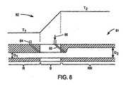
- FIG. 8shows an exemplary section 81 of an in line reactor, wherein two temperature profile regions (R and RR) and one buffer region (B) is shown.
- the temperature vs. distance curve of the section 81is also shown as plot 82 in the same figure.
- the section 81 in Figure 8has two different gaps.
- a gap of G 1is provided within the low temperature region R which is kept at a temperature of T 1 , and at the buffer region B.
- the gapchanges from G 1 to G 2 within the high temperature region RR, which is kept at a temperature of T 2 .
- the significance of this gap changewill now be discussed in relation with reacting a Cu/In/Ga/Se precursor stack on a foil substrate such as a Mo coated stainless steel web.
- the temperature T 1is about 100 C and the temperature T 2 is about 300 C.
- the webmoves from left to right within the gap of the reactor section 81 a portion of the precursor stack on the web gets heated from 100 C to 300 C by a rate that is determined by the speed of the web as discussed before.
- the temperature of the portionincreases, Cu, In, Ga and Se start reacting to form compounds.
- any excess Sestarts to vaporize since its vapor pressure is a strong function of temperature.
- the selenium vapor formed in the gapwould normally travel towards the cool end of the reactor, i.e. to the region R, and one there, would solidify since the temperature of region R is 100 C, which is lower than 217 C, the melting point of Se.
- a liquid phasemay also form within the gap in the buffer region B where temperature is at or higher than 217 C.
- gas inlets 83are placed near the edge of the high temperature region RR to direct a gas 80 from the smaller gap section towards the larger gap section of the reactor. Such gas flow pushes the Se vapors away from the colder sections towards the hotter sections.
- the gasmay be an inert gas such as N 2 and it may be introduced within the lower gap section also as indicated by inlet 84. Once the gas enters the gap it finds a lower resistance path flowing towards the larger gap region RR compared to the smaller gap region R. Therefore, a gas flow is established to discourage Se vapors entering the colder region R.
- Solar cellsmay be fabricated on the compound layers of the present invention using materials and methods well known in the field. For example a thin ( ⁇ 0.1 microns) CdS layer may be deposited on the surface of the compound layer using the chemical dip method. A transparent window of ZnO may be deposited over the CdS layer using MOCVD or sputtering techniques. A metallic finger pattern is optionally deposited over the ZnO to complete the solar cell.
- a thin ( ⁇ 0.1 microns) CdS layermay be deposited on the surface of the compound layer using the chemical dip method.
- a transparent window of ZnOmay be deposited over the CdS layer using MOCVD or sputtering techniques.
- a metallic finger patternis optionally deposited over the ZnO to complete the solar cell.
Landscapes
- Chemical & Material Sciences (AREA)
- Engineering & Computer Science (AREA)
- General Chemical & Material Sciences (AREA)
- Chemical Kinetics & Catalysis (AREA)
- Materials Engineering (AREA)
- Mechanical Engineering (AREA)
- Metallurgy (AREA)
- Organic Chemistry (AREA)
- Inorganic Chemistry (AREA)
- Physics & Mathematics (AREA)
- General Physics & Mathematics (AREA)
- Manufacturing & Machinery (AREA)
- Computer Hardware Design (AREA)
- Microelectronics & Electronic Packaging (AREA)
- Power Engineering (AREA)
- Condensed Matter Physics & Semiconductors (AREA)
- Photovoltaic Devices (AREA)
Description
- The present invention relates to method and apparatus for preparing thin films of semiconductor films for radiation detector and photovoltaic applications.
- Solar cells are photovoltaic devices that convert sunlight directly into electrical power. The most common solar cell material is silicon, which is in the form of single or polycrystalline wafers. However, the cost of electricity generated using silicon-based solar cells is higher than the cost of electricity generated by the more traditional methods. Therefore, since early 1970's there has been an effort to reduce cost of solar cells for terrestrial use. One way of reducing the cost of solar cells is to develop low-cost thin film growth techniques that can deposit solar-cell-quality absorber materials on large area substrates and to fabricate these devices using high-throughput, low-cost methods.
- Group IBIIIAVIA compound semiconductors comprising some of the Group IB (Cu, Ag, Au), Group IIIA (B, Al, Ga, In, Tl) and Group VIA (O, S, Se, Te, Po) materials or elements of the periodic table are excellent absorber materials for thin film solar cell structures. Especially, compounds of Cu, In, Ga, Se and S which are generally referred to as CIGS(S), or Cu(In,Ga)(S,Se)2 or CuIn1-xGax (SySe1-y)k, where 0≤x≤1, 0≤y≤1 and k is approximately 2, have already been employed in solar cell structures that yielded conversion efficiencies approaching 20%. Absorbers containing Group IIIA element Al and/or Group VIA element Te also showed promise. Therefore, in summary, compounds containing: i) Cu from Group IB, ii) at least one of In, Ga, and Al from Group IIIA, and iii) at least one of S, Se, and Te from Group VIA, are of great interest for solar cell applications.
- The structure of a conventional Group IBIIIAVIA compound photovoltaic cell such as a Cu(In,Ga,Al)(S,Se,Te)2 thin film solar cell is shown in
Figure 1 . Thedevice 10 is fabricated on asubstrate 11, such as a sheet of glass, a sheet of metal, an insulating foil or web, or a conductive foil or web. Theabsorber film 12, which comprises a material in the family of Cu(In,Ga,Al)(S,Se,Te)2 , is grown over aconductive layer 13, which is previously deposited on thesubstrate 11 and which acts as the electrical contact to the device. Various conductive layers comprising Mo, Ta, W, Ti, and stainless steel etc. have been used in the solar cell structure ofFigure 1 . If the substrate itself is a properly selected conductive material, it is possible not to use aconductive layer 13, since thesubstrate 11 may then be used as the ohmic contact to the device. After theabsorber film 12 is grown, atransparent layer 14 such as a CdS, ZnO or CdS/ZnO stack is formed on the absorber film.Radiation 15 enters the device through thetransparent layer 14. Metallic grids (not shown) may also be deposited over thetransparent layer 14 to reduce the effective series resistance of the device. The preferred electrical type of theabsorber film 12 is p-type, and the preferred electrical type of thetransparent layer 14 is n-type. However, an n-type absorber and a p-type window layer can also be utilized. The preferred device structure ofFigure 1 is called a "substrate-type" structure. A "superstrate-type" structure can also be constructed by depositing a transparent conductive layer on a transparent superstrate such as glass or transparent polymeric foil, and then depositing the Cu(In,Ga,Al)(S,Se,Te)2 absorber film, and finally forming an ohmic contact to the device by a conductive layer. In this superstrate structure light enters the device from the transparent superstrate side. A variety of materials, deposited by a variety of methods, can be used to provide the various layers of the device shown inFigure 1 . - In a thin film solar cell employing a Group IBIIIAVIA compound absorber, the cell efficiency is a strong function of the molar ratio of IB/IIIA. If there are more than one Group IIIA materials in the composition, the relative amounts or molar ratios of these IIIA elements also affect the properties. For a Cu(In,Ga)(S,Se)2 absorber layer, for example, the efficiency of the device is a function of the molar ratio of Cu/(In+Ga). Furthermore, some of the important parameters of the cell, such as its open circuit voltage, short circuit current and fill factor vary with the molar ratio of the IIIA elements, i.e. the Ga/(Ga+In) molar ratio. In general, for good device performance Cu/(In+Ga) molar ratio is kept at around or below 1.0. As the Ga/(Ga+In) molar ratio increases, on the other hand, the optical bandgap of the absorber layer increases and therefore the open circuit voltage of the solar cell increases while the short circuit current typically may decrease. It is important for a thin film deposition process to have the capability of controlling both the molar ratio of IB/IIIA, and the molar ratios of the Group IIIA components in the composition. It should be noted that although the chemical formula is often written as Cu(In,Ga)(S,Se)2, a more accurate formula for the compound is Cu(In,Ga)(S,Se)k, where k is typically close to 2 but may not be exactly 2. For simplicity we will continue to use the value of k as 2. It should be further noted that the notation "Cu(X,Y)" in the chemical formula means all chemical compositions of X and Y from (X=0% and Y=100%) to (X=100% and Y=0%). For example, Cu(In,Ga) means all compositions from CuIn to CuGa. Similarly, Cu(In,Ga)(S,Se)2 means the whole family of compounds with Ga/(Ga+In) molar ratio varying from 0 to 1, and Se/(Se+S) molar ratio varying from 0 to 1.
- The first technique that yielded high-quality Cu(In,Ga)Se2 films for solar cell fabrication was co-evaporation of Cu, In, Ga and Se onto a heated substrate in a vacuum chamber. However, low materials utilization, high cost of equipment, difficulties faced in large area deposition and relatively low throughput are some of the challenges faced in commercialization of the co-evaporation approach.
- Another technique for growing Cu(In,Ga)(S,Se)2 type compound thin films for solar cell applications is a two-stage process where metallic components of the Cu(In,Ga)(S,Se)2 material are first deposited onto a substrate, and then reacted with S and/or Se in a high temperature annealing process. For example, for CuInSe2 growth, thin layers of Cu and In are first deposited on a substrate and then this stacked precursor layer is reacted with Se at elevated temperature. If the reaction atmosphere also contains sulfur, then a CuIn(S,Se)2 layer can be grown. Addition of Ga in the precursor layer, i.e. use of a Cu/In/Ga stacked film precursor, allows the growth of a Cu(In,Ga)(S,Se)2 absorber.
- Sputtering and evaporation techniques have been used in prior art approaches to deposit the layers containing the Group IB and Group IIIA components of the precursor stacks. In the case of CuInSe2 growth, for example, Cu and In layers were sequentially sputter-deposited on a substrate and then the stacked film was heated in the presence of gas containing Se at elevated temperature for times typically longer than about 30 minutes, as described in
U.S. 4,798,660 . More recentlyU.S. Patent 6,048,442 disclosed a method comprising sputter-depositing a stacked precursor film comprising a Cu-Ga alloy layer and an In layer to form a Cu-Ga/In stack on a metallic back electrode layer and then reacting this precursor stack film with one of Se and S to form the absorber layer.U.S. Patent 6,092,669 described sputtering-based equipment for producing such absorber layers. Such techniques may yield good quality absorber layers and efficient solar cells, however, they suffer from the high cost of capital equipment, and relatively slow rate of production. - Two-stage process approach may also employ stacked layers comprising Group VIA materials. For example, a Cu(In,Ga)Se2 film may be obtained by depositing In-Ga-selenide and Cu-selenide layers in a stacked manner and reacting them in presence of Se. Similarly, stacks comprising Group VIA materials and metallic components may also be used. In-Ga-selenide/Cu stack, for example, may be reacted in presence of Se to form Cu(In,Ga)Se2.
- Reaction step in a two-stage process is typically carried out in batch furnaces where a large number of substrates are processed. One prior art method described in
U.S. Patent 5,578,503 utilizes a rapid thermal annealing approach to react precursor layers in a "single-substrate" manner. In the "single-substrate" RTP approaches, the precursor film on a single base or substrate is loaded into a RTP reactor which is at room temperature, or at a temperature of < 100 C. The precursor film may comprise, for example, Cu, In, Ga and Se. Alternately, the precursor may comprise Cu, In and Ga and Se may be provided from a vapor phase in the reactor. The reactor is then sealed and evacuated to eliminate air/oxygen from the reaction environment. After evacuation, the reactor is backfilled with a gas and process is initiated. Reaction is typically carried out by varying or profiling the reactor temperature or the substrate temperature. A typical temperature profile used for CIGS film formation is shown inFigure 6 . The heating of the reactor and the precursor film is initiated at time to and the temperature is raised to a first plateau T1 within a time period Δ1. The temperature T1 may be in the range of 200-300 C. It is reported that ( V. Probst et al., MRS Symposium Proc. Vol. 426, 1996, p. 165) the rate of temperature increase during this time period Δ1 is important, especially for precursor layers comprising a Se sub-layer on the surface of a metallic sub-layer comprising Cu, In and Ga. According to the above reference, this heating-up rate should be in the range of 10 C/sec to avoid excessive melting of Se which may deteriorate the morphology of the film being formed. After a period Δ2 of initial reaction, temperature is again increased during the time interval Δ3 between times t2 and t3 settling at a value T2, which may be in the range of 450-550 C. After a reaction time period Δ4, a cool-down period Δ5 is initiated at time t4 to bring the temperature of the reactor and the film, down to a level to allow safe unloading of the base or the substrate carrying the formed CIGS compound layer. This unload temperature is typically below 100 C, preferably below 60 C. - It should be appreciated that a "single-substrate" processing approach described above is time consuming since it involves evacuation, temperature cycling and then cooling down of the reactor for each loaded substrate. Also heating the reactor up to temperatures above 500 C and then cooling it down to room temperature or at least to a temperature of < 100 C, repeatedly, in a production environment may cause reliability issues. Since this is a "single substrate reaction" approach, very large area reactors are needed to increase the throughput. Furthermore, achieving very high heating rates (>10 C/sec) requires large amount of power at least during the heat-up periods of the temperature profile such as the one shown in
Figure 6 . - Irrespective of the specific approach used in a two-stage process, growing for example a Cu(In,Ga)(S,Se)2 absorber film, individual thicknesses of the layers forming the precursor stacked structure need to be controlled so that the two molar ratios mentioned before, i.e. the Cu/(In+Ga) ratio and the Ga/(Ga+In) ratio, can be kept under control from run to run and on large area substrates. The molar ratios attained in the stacked structures are generally preserved in macro scale during the reaction step, provided that the reaction temperature is kept below about 600 °C. Therefore, the overall or average molar ratios in the compound film obtained after the reaction step is, generally speaking, about the same as the average molar ratios in the precursor stacked structures before the reaction step.
- Selenization and/or sulfidation of precursor layers comprising metallic components may be carried out in various ways. One approach involves using gases such as H2Se, H2S or their mixtures to react, either simultaneously or consecutively, with the precursor comprising Cu, In and/or Ga. This way a Cu(In,Ga)(S,Se)2 film is formed after annealing and reacting at elevated temperatures. It is possible to increase the reaction rate or reactivity by striking a plasma in the reactive gas during the process of compound formation. Se vapors or S vapors from elemental sources may also be used for selenization and sulfidation. Alternately, Se and/or S may be deposited over the precursor layer comprising Cu, In and/or Ga and the stacked structure can be annealed at elevated temperatures to initiate reaction between the metallic elements or components and the Group VIA material(s) to form the Cu(In,Ga)(S,Se)2 compound.
- Design of the reaction chamber to carry out selenization/sulfidation processes is critical for the quality of the resulting compound film, the efficiency of the solar cells, throughput, material utilization and cost of the process. Present invention resolves many of the non-uniformity, uncontrolled reaction rate issues and provide high-quality, dense, well-adhering Group IBIIIAVIA compound thin films with macro-scale as well as micro-scale compositional uniformities on selected substrates. Since the reactor volume is small, material cost is also reduced especially for the reaction gases. Small mass of the reactors increase processing speed and throughput.
- The present invention relates to method and apparatus for preparing thin films of semiconductor films for radiation detector and photovoltaic applications.
- In one aspect, the present invention includes a series of chambers between the inlet and the outlet, with each chamber having a gap that allows a substrate to pass therethrough, and which is temperature controlled, thereby allowing each chamber to maintain a different temperature, and the substrate to be annealed based upon a predetermined temperature profile by efficiently moving through the series of chambers at a predetermined speed profile.
- In another aspect, each of the chambers opens and closes, and creates a seal when in the closed position during which time annealing takes place within the gap of the chamber.
- In a further aspect, the present invention provides a method of forming a Group IBIIIAVIA compound layer on a surface of a flexible roll. The method includes depositing a precursor layer comprising at least one Group IB material and at least one Group IIIA material on the surface of the flexible roll, providing at least one Group VIA material to an exposed surface of the precursor layer; and annealing, after or during the step of providing, the flexible roll using a series of process chambers, the step of annealing including feeding the flexible roll having the deposited precursor layer thereon from an inlet, through the series of process chambers to an outlet, each process chamber having a gap therein set to a predetermined temperature, thereby applying the predetermined temperature to a section of the flexible roll within the gap associated therewith.
- These and other aspects and features of the present invention will become apparent to those of ordinary skill in the art upon review of the following description of specific embodiments of the invention in conjunction with the accompanying figures, wherein:
FIG. 1 is a cross-sectional view of a solar cell employing a Group IBIIIAVIA absorber layer.FIG. 2 shows an apparatus to form a Group IBIIIAVIA layer.FIG. 3A shows a cross-sectional sketch of a process chamber with upper and lower bodies moved away from each other.FIG 3B shows a cross-sectional sketch of a process chamber with upper and lower bodies moved towards each other for sealing one portion of the substrate for processing in the chamber.FIG. 3C shows another process chamber in sealed position.FIG 3D shows another process chamber.FIG. 4 shows a processing unit comprising multiple sections for multiple processes.FIG. 5 shows a processing unit enclosed by a secondary enclosure.FIG. 6 shows a temperature profile used in a RTP approach.FIG. 7 shows a small gap reactor and its temperature profile.FIG. 8 shows a section of a variable gap reactor.- Reaction of precursors, comprising Group IB material(s), Group IIIA material(s) and optionally Group VIA material(s) or components, with Group VIA material(s) may be achieved in various ways. These techniques involve heating the precursor layer to a temperature range of 350-600 °C in the presence of at least one of Se, S, and Te provided by sources such as solid Se, solid S, solid Te, H2Se gas, H2S gas, H2Te gas, Se vapors, S vapors, Te vapors etc. for periods ranging from 1 minute to 1 hour. The Se, S, Te vapors may be generated by heating solid sources. Hydride gases such as H2Se and H2S may be bottled gases. Such hydride gases and short-lifetime gases such as H2Te may also be generated in-situ, for example by electrolysis in aqueous acidic solutions of cathodes comprising S, Se and/or Te, and then provided to the reactors. Electrochemical methods to generate these hydride gases are suited for in-situ generation. Precursor layers may be exposed to more than one Group VIA materials either simultaneously or sequentially. For example, a precursor layer comprising Cu, In, Ga, and Se may be annealed in presence of S to form Cu(In,Ga)(S,Se)2. The precursor layer in this case may be a stacked layer comprising a metallic layer containing Cu, Ga and In and a Se layer that is deposited over the metallic layer. Alternately, Se nano-particles may be dispersed throughout the metallic layer containing Cu, In and Ga. It is also possible that the precursor layer comprises Cu, In, Ga and S and during reaction this layer is annealed in presence of Se to form a Cu(In,Ga)(S,Se)2. Some of the preferred approaches of forming a Cu(In,Ga)(S,Se)2 compound layer may be summarized as follows: i) depositing a layer of Se on a metallic precursor comprising Cu, In and Ga forming a structure and reacting the structure in gaseous S source at elevated temperature, ii) depositing a mixed layer of S and Se or a layer of S and a layer of Se on a metallic precursor comprising Cu, In and Ga forming a structure, and reacting the structure at elevated temperature in either a gaseous atmosphere free from S or Se, or in a gaseous atmosphere comprising at least one of S and Se, iii) depositing a layer of S on a metallic precursor comprising Cu, In and Ga forming a structure and reacting the structure in gaseous Se source at elevated temperature, iv) depositing a layer of Se on a metallic precursor comprising Cu, In and Ga forming a structure, and reacting the structure at elevated temperature to form a Cu(In,Ga)Se2 layer and then reacting the Cu(In,Ga)Se2 layer with a gaseous source of S, liquid source of S or a solid source of S such as a layer of S, v) depositing a layer of S on a metallic precursor comprising Cu, In and Ga forming a structure, and reacting the structure at elevated temperature to form a Cu(In,Ga)S2 layer, and then reacting the Cu(In,Ga)S2 layer with a gaseous source of Se, liquid source of Se or a solid source of Se such as a layer of Se.
- It should be noted that Group VIA materials are corrosive. Therefore, materials for all parts of the reactors or chambers that are exposed to Group VIA materials or material vapors at elevated temperatures should be properly selected. These parts should be made of or should be coated by substantially inert materials such as ceramics, e.g. alumina, tantalum oxide, titania, zirconia etc., glass, quartz, stainless steel, graphite, refractory metals such as Ta, refractory metal nitrides and/or carbides such as Ta-nitride and/or carbide, Ti-nitride and/ or carbide, W-nitride and/or carbide, other nitrides and/or carbides such as Si-nitride and/or carbide, etc.
- In another embodiment, a layer or multi layers of Group VIA materials are deposited on the precursor layer or stacks or mixtures of Group IB, Group IIIA and Group VIA materials are formed, and the stacked layers are then heated up in a furnace, in a rapid thermal annealing furnace, or laser annealing system and like to cause intermixing and reaction between the precursor layer and the Group VIA materials. Group VIA material layers may be obtained by evaporation, sputtering, or electroplating. Alternately inks comprising Group VIA nano particles may be prepared and these inks may be deposited to form a Group VIA material layer comprising Group VIA nano particles. Other liquids or solutions such as organo-metalic solutions comprising at least one Group VIA material may also be used. Dipping into melt or ink, spraying melt or ink, doctor-blading or ink writing techniques may be employed to deposit such layers.
- As described above, it is also possible to use the above mentioned selenization and/or sulfidation techniques together, e.g. have a solid film of group VIA material on the precursor layer and carry out reaction in Group VIA material vapor or gases. Reaction may be carried out at elevated temperatures for times ranging from 1 minute to 60 minutes depending upon the temperature, the film thickness and exact composition and morphology of the precursor layer. As a result of reaction, the Group IBIIIAVIA compound is formed from the precursor.
- One
apparatus 500 to carry out the reaction step of a precursor layer to form a Group IBEIIAVIA compound film is shown inFigure 2 . It should be noted that the precursor layer to be reacted in this reactor may comprise at least one Group IB material and at least one Group IIIA material. For example the precursor layer may be a stack of Cu/In/Ga, Cu-Ga/In, Cu-In/Ga, Cu/In-Ga, Cu-Ga/Cu-In, Cu-Ga/Cu-In/Ga, Cu/Cu-In/Ga, or Cu-Ga/In/In-Ga etc., where the order of various material layers within the stack may be changed. Here Cu-Ga, Cu-In, In-Ga mean alloys or mixtures of Cu and Ga, alloys or mixtures of Cu and In, and alloys or mixtures of In and Ga, respectively. Alternatively, the precursor layer may also include at least one Group VIA material. There are many examples of such precursor layers. Some of these are Cu/In/Ga/Group VIA material stack, Cu-Group VIA material/In/Ga stack, In-Group VIA material/Cu-Group VIA material stack, or Ga-Group VIA material/Cu/In, where Cu-Group VIA material includes alloys, mixtures or compounds of Cu and a Group VIA material (such as Cu-selenides, Cu sulfides, etc.), In-Group VIA material includes alloys, mixtures or compounds of In and a Group VIA material (such as In-selenides, In sulfides, etc.), and Ga-Group VIA material includes alloys, mixtures or compounds of Ga and a Group VIA material (such as Ga-selenides, Ga sulfides, etc.). These precursors are deposited on a base comprising asubstrate 11, which may additionally comprise aconductive layer 13 as shown inFigure 1 . Other types of precursors that may be processed using the method and apparatus of the invention includes Group IBIIIAVIA material layers that may be formed on a base using low temperature approaches such as compound electroplating, electroless plating, sputtering from compound targets, ink deposition using Group IBIIIAVIA nano-particle based inks etc. These material layers are then annealed in the apparatus or reactors at temperatures in the 200-600 °C range to improve their crystalline quality, composition and density. - Annealing and/or reaction steps may be carried out in the reactors of the present invention at substantially the atmospheric pressure, at a pressure lower than the atmospheric pressure or at a pressure higher than the atmospheric pressure. Lower pressures in reactors may be achieved through use of vacuum pumps. For low pressure and high pressure reactors sealing need to be provided not to let outside air to get into the reactor or the reactive gases to get out. During reaction of the precursor layers with Group VIA materials, use of high reaction pressure may be advantageous to increase reactivity of the Group VIA materials and to increase their boiling temperatures. Higher pressure may be obtained in the reactors through overpressure of the Group VIA material species or through increased partial pressure of other gasses such as nitrogen, hydrogen and helium that may be used in the reactor. After the reaction is complete it may be beneficial to heat the formed compound layers in low pressure reactors. This would get the excess Group VIA materials off the formed compound layers and improve their electrical, mechanical and compositional properties.
- The
apparatus 500 comprises a series ofchambers 501 that are placed next to each other in a linear fashion. Thechambers 501 may be separated from each other by asmall gap 502, or alternately allchambers 501 may structurally be connected to each other, however they may be internally separated through use of seals or spacers as will be discussed later. Thechambers 501 comprise anupper body 503 and alower body 504 that are separable from each other by a predetermined distance. A base orsubstrate 505 has a width of W and enters theapparatus 503 atinlet 506 and exits theapparatus 503 at anoutlet 507. Thesubstrate 505 may be a continuous web or sheet of a metal or an insulator comprising a precursor layer to be reacted to form the compound film. Alternately there may be a carrier on which pre-cut substrates comprising the precursor layers may be placed. The carrier may then carry these pre-cut substrates through various process chambers. There are mechanisms (not shown) that move the substrate laterally through theapparatus 500 and move theupper body 503 and/or thelower body 504 of the process chambers to achieve relative motion between the upper and lower bodies. Preferably, the substrate may be moved by an increment from left to right after theupper body 503 is moved away from thelower body 504 and then subsequently theupper body 503 andlower body 504 are brought closer to sandwich the substrate (or carrier in case a carrier is used) between them and the processing is carried out for a predetermined period of time. Figure 3A shows in more detail a cross-sectional view of achamber 501. In this figure theupper body 503 is moved away from thelower body 504, and asection 509 of thesubstrate 505 is placed between theupper body 503 and the lower body 504.Thesubstrate 505 comprises aprecursor layer 508 that is to be processed. Theupper body 503 has ashallow cavity 511 and thelower body 504 is substantially flat. In a preferred embodiment the length of thesection 509 may be (15,2-152 cm (0.5-5 ft), whereas the depth of thecavity 511 may be in the range of 0.5-10 mm, more preferably 1-5 mm. The width of the substrate may be in the range of 15,2-305 cm (0.5-10 ft), preferably 30,5-152 cm (1-5 ft). Once thesection 509 of thesubstrate 505 is in place, either theupper body 503 or thelower body 504 or both are moved towards each other untilspacer 510 makes contact with or comes to close proximity (within about 1 mm) of theprecursor layer 508 as shown inFigure 3B . This way aprocess gap 512 is formed above theprecursor layer 508 and theupper body 503. It should be noted that thespacer 510 may seal the process gap if high temperature sealing materials are used as spacers. Alternately, the spacer may be a leaky seal and a positive gas pressure may be kept within theprocess gap 512 so that undesirable gases do not leak from outside into theprocess gap 512 during processing.- As can be seen from
Figure 3B the seal or leaky seal is made against or onto the precursor layer or the substrate. An alternative embodiment is shown inFigure 3C where the seal or leaky seal is made against or onto acarrier 516 which carries apre-cut substrate 517 comprising aprecursor layer 518 into thechamber 519. In this case some of the details of thechamber 519, such as gas inlets, outlets etc. are not shown to simplify the figure. We will now continue describing the invention using the chamber design shown inFigures 3A and 3B . It should be understood that variants of this design and the design shown inFigure 3C may also be used in a similar manner. - As the
section 509 of thesubstrate 505 is being moved into the chamber 501 agas 515 may be flown through at least one of thegas tubes precursor layer 508 and thespacer 510 as shown by the arrows inFigure 3A . This way atmospheric gases and especially oxygen within thenarrow process gap 512 above the precursor layer surface may be replaced with the gas flown through the gas tubes in a very short period of time such as within 1-10 seconds. This is important for throughput of the process as well as the quality of the compound film formed because when thesection 509 of the substrate is at position shown inFigure 3A , thelower body 504 may already be heated and may start to heat theprecursor layer 508. To avoid reaction of theprecursor layer 508 with the undesired atmosphere, there is a need to replace the atmosphere very quickly with a controlled atmosphere that may be provided by the gas flown through the gas tubes into theprocess gap 512. In the example ofFigure 3A bothgas tubes gas 515 may be an inert gas such as nitrogen, argon or helium or a reducing gas such as a mixture of hydrogen (e.g. 2-5% mixture) with any inert gas. This way the atmosphere left over from the previous process step in the cavity is quickly replaced with a fresh inert or reducing atmosphere by the time thespacer 510 comes in close proximity of theprecursor layer 508 forming theprocess gap 512. Once processing starts additional gases such as reactive gases may then be flown into theprocess gap 512 and some of thegas inlets 515 may be used as gas outlets such as shown inFigure 3B . Alternately there may be different sets of dedicated gas inlets and gas outlets. The small gap reactor shown inFigure 3B is well suited for plasma generation within the process gap. Activity enhancing methods such as plasma generation very close to the processed film surface accelerates reaction and reduces processing time. For example, presence of plasma within the process gap enhances reaction rate of Group VIA material with the precursor layer and accelerates formation of Group IBIIIAVIA compound layer. Alternately, the gas entering the process gap may be passed through a plasma, just before it enters the process gap. For example, a gas comprising Group VIA material may be passed through a plasma chamber outside and then flown into the process gap with the activated Group VIA material species. This also increases the process throughput. - The base or substrate may be engaged onto the lower body surface by various means including keeping the substrate under tension (in case of flexible web substrates), magnetic coupling, electrostatic chuck etc. Close mechanical contact between the lower body surface and the substrate is important, especially in cases where the temperature of the substrate is controlled by the temperature of the lower body as we will discuss later.
- Although a preferred geometry of the chamber is shown in
Figures 3A, 3B and 3C , several changes may be made to the design. For example, instead of being lateral, the chambers may be placed vertically and the substrate may travel through them in a vertical manner. Similarly the chamber may be rotated 180 degrees and process may be applied to the precursor layer while the precursor layer faces down in order to avoid particles dropping on its surface during reaction. There may be an additional cavity or alower cavity 518 shown as dotted lines inFigure 3B in thelower body 504 and the substrate may be suspended between thecavity 512 and thelower cavity 513. There may be gas lines bringing in and carrying out gases to and from thelower cavity 513. It is also possible to eliminate thecavity 511 and touch the precursor layer surface during the process by theupper body 503 to achieve a near-zero gap between the exposed surface of the precursor layer and theupper body 503. At least part of theupper body 503 facing theprecursor layer 508 may be made porous to allow gasses or vapors to be fed towards the precursor layer surface in a diffused and well distributed manner. This is shown inFigure 3D wherein the chamber is shown with aporous section 520 which is in physical contact or in close proximity (within about 1 mm) of the precursor layer. There may additionally be heating means (not shown) such as heater coils within the porous section to control its temperature. - In any of the reactors as described above, during reaction, a mechanism can be included that allows for relative motion and physical contact between the precursor layer and a soft high-temperature material, such as quartz wool. The relative motion between the soft high-temperature material and the precursor layer may distribute the reactant more uniformly to yield better uniformity in reaction.
- In one preferred embodiment (see
Figure 3B ) thelower body 504 of thechamber 519 may be held at the process temperature such as at a temperature of 200-600 °C, and as soon as the seal or leaky seal is made by thespacer 510,process gas 550 may start flowing into theprocess gap 512 and annealing and/or reaction starts within the precursor layer. As already described, a gas 515 (seeFigure 3A ) is previously flown to replace any unwanted gases or atmosphere (such as air) within theprocess gap 512 before theprocess gas 550 starts to come into theprocess gap 512. It is possible that thegas 515 and theprocess gas 550 are the same gas, for example nitrogen. This depends on the nature of theprecursor layer 508. In general, if theprecursor layer 508 comprises Group VIA material(s) such as Se, then theprocess gas 550 may be an inert gas such as nitrogen, argon or helium, and during reaction the Group VIA material within the precursor layer reacts with the Group IB and Group IIIA materials forming the Group IBIIIAVIA compound layer. Otherwise, the process gas may comprise species comprising the Group VIA material, to provide to the reaction or to keep certain overpressure of the volatile Group VIA material over the surface of the reacting precursor layer. Therefore, theprocess gas 550 may comprise Se vapor, S vapor, H2Se, H2S, etc. Furthermore it is possible to change the gas during the process. For example, at the beginning of the process theprocess gas 550 may comprise Se. Later in the process, after the precursor reacts with Se and forms Cu(In,Ga)Se2 the gas may be changed to an inert gas and annealing may be performed for grain growth and/or for making the Ga concentration profile within the film more uniform. Alternately after the formation of the Cu(In,Ga)Se2 layer, the process gas may change into one comprising S to convert the film into a Cu(In,Ga)(S,Se)2 layer. These process steps may be carried out in a single chamber such as the ones shown inFigures 3A, 3B, 3C and3D , or each step may be carried out in a dedicated chamber in a system with multiple chambers in a line such as the system shown inFigure 2 , or in a cluster system employing a central robot that carries substrates to and from multiple process chambers. In addition to thelower body 504, theupper body 503 may also be heated to assure temperature uniformity over the section of the substrate within the chamber and also to avoid excessive precipitation of the Group VIA volatile species on the upper body walls. There may be holes in the lower body 504 (not shown) ofFigures 3A, 3B, 3C and3D that can direct a gas stream to the bottom side of thesubstrate 505. When the reaction step is over, for example, a gas such as nitrogen may be directed to the back side of the substrate as theupper body 503 is moved up. This way the thermal coupling is broken between the substrate and thelower body 504 by floating the substrate on a thin blanket of gas. By controlling the composition of the gas (selecting high thermal conductivity or low thermal conductivity gases or their mixtures) the cooling rate of the substrate may also be controlled. - Above embodiment described a case where the process temperature or reaction temperature was mainly controlled by the temperature of the
lower body 504 with optional heating means within theupper body 503. In this case, if a varying process temperature profile is needed (for example temperature stepping from room temperature to 150-250 °C range and staying there 0.5-15 minutes and then increasing to 400-600 °C and staying there for an additional 0.5-5 minutes) the temperature of thelower body 504 may be changed rapidly to achieve the desired temperature-time profile for the process. Alternatively, in a multi chamber system such as the one inFigure 2 , one chamber, such as chamber A may have the lower body temperature set at one temperature, such as to the 150-250 °C range, and the next chamber B may have the lower body temperature set at another temperature, such as at a range of 400-600 °C. A specific section of the substrate is then first processed in chamber A for 0.5-15 minutes and then moved to chamber B to get processed for an additional 0.5-15 minutes at the higher temperature. This way different sections of the substrate, which may either be a single piece or a pre-cut piece (seeFigure 3C ), get processed in different chambers under different conditions. This is a "stepped, in-line" process that offers flexibility of changing temperatures and reaction atmospheres rapidly in a high throughput process. During the motion of the substrate sections between chambers the upper body and lower body of the chambers move away from each other forming a narrow slit allowing the substrate or the carrier to move. During this time inert gases may be flown into the chambers and flood thegaps 502 to protect the hot portions of the precursor layer or the partially reacted layer from reacting with the environment outside the chambers. If the gaps are eliminated and/or a secondary enclosure (not shown) is placed around theapparatus 500, then the atmosphere outside thechambers 501 may also be controlled. For example, the secondary enclosure may continuously be flushed with nitrogen assuring nonreactive environment. An example of asecondary enclosure 700 is shown inFigure 5 as applied to a process unit processing flexible foil substrates. In this case asupply spool 701 and a receivingspool 702 for the flexible substrate is placed in thesecondary enclosure 700 along with amulti chamber system 703, which may be a processing unit or apparatus such as the one depicted inFigure 2 .Secondary enclosure 700 may have at least onedoor 704 for access, at least onegas line 705 for flowing gasses in and out of theenclosure 700 and/or pulling vacuum in theenclosure 700. Appropriate number ofvalves 706 may be used to shut off gas flows or vacuum when necessary. It should be appreciated that a two level reactor design such as the one shown inFigure 5 allows flexibility of controlling the atmosphere around the reactors which are within themulti-chamber system 703. For the case of processing rigid substrates such as glass sheets in a step-wise continuous manner a load port and an unload port or load-locks may be placed on the left and right side of theenclosure 700. These ports or load-locks may seal the inside volume of theenclosure 700 from outside atmosphere during substrate transfer into theenclosure 700. - In another embodiment the process temperature is mainly determined by the
upper body 503. In this case thelower body 504 may be at room temperature or at a predetermined constant temperature that may be less than 150 °C. A gas with low thermal conductivity, such as nitrogen (0.026 W/m), may be flown until the seal or leaky seal is established (seeFigure 3A ). During this time the temperature of the precursor layer is controlled by thelower body 504. Once the seal is established a high thermal conductivity gas such as He (0.156 W/m) and/or H2 (0.18 W/m) may be introduced in theprocess gap 512 along with other desired ingredients such as Group VIA material vapors. Due to thermal coupling of the precursor layer to theupper body 503 through the thermally conductive gas, the temperature of the precursor layer may be raised towards the temperature of theupper body 503 and the process of reaction may be initiated. In this example the temperature of the upper body may be controlled in the range of 200-600 °C. - Alternately, in a design with two cavities (see
Figure 3B ), both the temperature of thelower body 504 and the temperature of theupper body 503 may play a role in determining the temperature of the precursor layer or the process temperature. In this case if, for example, a high thermal conductivity gas is flown into theupper cavity 511 and a low thermal conductivity gas is flown into the lower cavity, the temperature of the substrate or the precursor layer will be mostly determined by the temperature of theupper body 503. If, on the other hand, a high thermal conductivity gas is flown into thelower cavity 513 and a low thermal conductivity gas is flown into theupper cavity 511, the temperature of the substrate or the precursor layer will be mostly determined by the temperature of thelower body 504. By changing composition of gasses in the upper and lower cavities therefore, different temperature-time profiles may be achieved using this design. - An example will now be given to describe one embodiment of the present invention.
- Example: A Mo coated stainless steel or aluminum foil may be used as the base. A metallic precursor comprising Cu, In, and Ga may be deposited on the base.
Multi-chamber process unit 603 shown inFigure 4 may be used for the formation of a Cu(In,Ga)(S,Se)2 layer on the base. The base comprising the metallic precursor layer is depicted inFigure 4 assubstrate 602. Theprocess unit 603 has chambers or sections indicated by dotted lines and labeled as A, B, C, D and E. The process unit has a singletop body 600 and a singlebottom body 601. Within thetop body 600 and thebottom body 601 there are independent heating means to independently change and control temperatures of the individual sections A, B, C, D and E. There are alsoindependent gas lines 604 that may act as gas inlets or outlets for each section. - In this example, section A is used for Se deposition on the metallic precursor. Section B is used for initial reaction at a temperature of 150-250 °C. Section C is used for complete reaction at 400-600 °C. Section D is used for S inclusion and section E is used for annealing.
- During processing, a first portion of the
substrate 602 is placed in section A of theprocess unit 603. After sealing, gas line in section A brings in Se vapor which condenses and forms a Se layer on the metallic precursor in the first portion of thesubstrate 602. Next thetop body 600 and thebottom body 601 are slightly separated from each other and thesubstrate 602 is moved bringing the first portion of the substrate into section B of theprocess unit 603 while bringing a second portion of the substrate into the section A of theprocess unit 603. Thetop body 600 and/or thebottom body 601 are then moved towards each other to establish seals or leaky seals for all the sections. This time, while the initial reaction step is carried out on the first portion of the substrate, a selenium deposition step is carried out on the second portion. The initial reaction step may comprise partially reacting the metallic precursor layer with the deposited Se layer at a temperature, preferably below the melting temperature of Se as to avoid flow patterns and non-uniformities on the forming compound layer. After the initial reaction step is completed, the substrate is moved again as described before, bringing the first portion into section C, the second portion into section B and a third portion into section A. In section C a high temperature reaction is carried out at temperatures above 400 °C for a period that may range from 0.5 minutes to 15 minutes. During this step, additional Se containing gases may be introduced into the process gap in section C to make sure there is excess Se overpressure in the reaction environment. It should be noted that as the high temperature reaction is carried out on the first portion of the substrate in section C of theprocess unit 603, Se deposition is carried out in section A on the third portion of the substrate and the initial reaction step is carried out on the second portion in section B. - In the next step of the overall process the first portion of the substrate is exposed to S containing environment in section D of the
process unit 603 at elevated temperatures of 400-600 °C for a time period in the range of 0.5-15 minutes. During this process step some of the Se in the Cu(In,Ga)Se2 layer formed in section C is replaced by S forming a Cu(In,Ga)(S,Se)2 compound film. The last section E of theprocess unit 603 may be used for additional annealing for grain growth and/or compositional uniformity improvement or for the purpose of stepwise cooling down the substrate. - The example above utilizes a series configuration for the process unit where the processing time is determined by the longest process step. It is of course within the scope of this invention to form a process unit running different process steps in parallel, through for example the use of a cluster tool.
- The tool or reactor designs of this invention may also be used for continuous, in-line processing of substrates which may be in the form of a web or in the form of large sheets such as glass sheets which may be fed into the reactor in a continuous manner. We will describe these aspects using roll-to-roll web processing in the examples below.
- The disadvantages of the prior-art "single-substrate" RTP approaches, where the temperature of the RTP chamber is raised and lowered continually during processing, were previously discussed. The in-line RTP reactor designs of the present invention are flexible, lower-cost and higher throughput, and they specifically are suited for CIGS(S) type of compound film formation.
Figure 7 shows a cross sectional schematic of a small-gap, in-line,RTP reactor 70 comprising multiple sections or regions. There are four temperature profile regions (R1, R2, R3, R4) and three buffer regions (B1, B2, B3) within thetop body 71 andbottom body 72 of thereactor 70. Asubstrate 74 or a base is fed through thegap 75 of thereactor 70 in the direction ofarrow 76. Thesubstrate 74 may be a foil with a precursor layer (not shown) on it, precursor comprising Cu, In, Ga and optionally at least one of Se and S. The goal is to convert the precursor on a given section of thesubstrate 74 into a CIGS(S) compound as the given section of thesubstrate 74 exits the reactor on the right hand side. - The temperature profile regions have heating means 77 and cooling means 78 distributed in the
top body 71 and thebottom body 72. The heating means 77 may be heater elements such as heater rods. Cooling means 78 may be cooling coils circulating a cooling gas or cooling liquid. Although the buffer regions may also have heating and cooling means, preferably they do not contain such means. Preferably the buffer regions are made of low thermal conductivity materials such as ceramics so that they can sustain a temperature gradient across them as shown by thereactor profile 73. The heating means 77 and cooling means are distributed to obtain thereactor profile 73. For example, the last region R4 and the lower temperature ends of the buffer regions B1 and B2 may have cooling means 78 while heating means 77 may be distributed everywhere else. - The
reactor profile 73 is an exemplary temperature vs. distance profile of thereactor 70. It should be noted that thereactor profile 73 is different from the temperature vs. time plot of a "single-substrate" reactor shown inFigure 6 . The temperature vs. time plot ofFigure 6 shows the temperature profile experienced by a substrate placed in the "single-substrate" reactor. The temperature vs. time profile experienced by any section of thesubstrate 74 in thereactor 70 ofFigure 7 can be changed and controlled by changing and controlling the speed at which thesubstrate 74 is moved from left to right through thegap 75. For example, if the distance L1 is 5 cm and thesubstrate 74 is moved at a velocity of 1 cm/second, then a point on thesubstrate 74 will pass through the buffer region B1 in 5 seconds. If, for example, the temperatures at the left and right ends of the buffer region B1 are 100 C and 300 C, this means that the point on thesubstrate 74 will experience a temperature profile that goes from 100 C to 300 C in 5 seconds. This corresponds to a heating rate of 40 C/seconds. As can be appreciated, reaching such heating rates in a "single-substrate" reactor is very difficult and requires very high power density. For the in-line RTP reactor ofFigure 7 , however, thereactor profile 73 is established once and then it stays unchanged. By changing the velocity of the substrate the temperature profile experienced by the substrate may be changed at will. Lack of heating and cooling the reactor continually in a cyclic manner increases reliability and reduces power consumption. - As described previously, more sections may be added to the reactor design of
Figure 7 . Each section may perform a different function such as reacting Cu, In, Ga with Se, reacting the already formed Cu(In,Ga)Se2 with S, annealing the already formed compound layer in an inert atmosphere etc. These sections may be separated from each other by soft barriers that may touch the surface of the already reacted precursor layer. Such barriers may be made of high temperature materials such as high temperature fibers or wools. This way cross talk between various sections of the reactor is minimized, especially if different gases are introduced in different sections. - It is also possible to change the gap of the reactor between or within each temperature profile region or buffer region.
Figure 8 shows anexemplary section 81 of an in line reactor, wherein two temperature profile regions (R and RR) and one buffer region (B) is shown. The temperature vs. distance curve of thesection 81 is also shown asplot 82 in the same figure. Thesection 81 inFigure 8 has two different gaps. A gap of G1 is provided within the low temperature region R which is kept at a temperature of T1, and at the buffer region B. The gap changes from G1 to G2 within the high temperature region RR, which is kept at a temperature of T2. The significance of this gap change will now be discussed in relation with reacting a Cu/In/Ga/Se precursor stack on a foil substrate such as a Mo coated stainless steel web. - Let us assume that the temperature T1 is about 100 C and the temperature T2 is about 300 C. As the web (not shown) moves from left to right within the gap of the reactor section 81 a portion of the precursor stack on the web gets heated from 100 C to 300 C by a rate that is determined by the speed of the web as discussed before. When the temperature of the portion increases, Cu, In, Ga and Se start reacting to form compounds. At the same time any excess Se starts to vaporize since its vapor pressure is a strong function of temperature. The selenium vapor formed in the gap would normally travel towards the cool end of the reactor, i.e. to the region R, and one there, would solidify since the temperature of region R is 100 C, which is lower than 217 C, the melting point of Se. Similarly a liquid phase may also form within the gap in the buffer region B where temperature is at or higher than 217 C. As a result as more and more portions of the web enter the reactor and get processed, more and more Se accumulation may be observed in the colder sections of the reactor and eventually the gap may be filled with Se. Therefore, measures need to be taken to stop Se vapors from diffusing to the cold sections or regions of the reactor. In the variable gap design of
Figure 8 ,gas inlets 83 are placed near the edge of the high temperature region RR to direct agas 80 from the smaller gap section towards the larger gap section of the reactor. Such gas flow pushes the Se vapors away from the colder sections towards the hotter sections. It should be noted that the gas may be an inert gas such as N2 and it may be introduced within the lower gap section also as indicated byinlet 84. Once the gas enters the gap it finds a lower resistance path flowing towards the larger gap region RR compared to the smaller gap region R. Therefore, a gas flow is established to discourage Se vapors entering the colder region R. - Solar cells may be fabricated on the compound layers of the present invention using materials and methods well known in the field. For example a thin (<0.1 microns) CdS layer may be deposited on the surface of the compound layer using the chemical dip method. A transparent window of ZnO may be deposited over the CdS layer using MOCVD or sputtering techniques. A metallic finger pattern is optionally deposited over the ZnO to complete the solar cell.
Claims (40)
- An in-line reactor to process a substrate according to a predetermined temperature profile,
the reactor comprising;
a substrate inlet;
a substrate outlet;
a series of chambers between the inlet and the outlet, each chamber including:an upper body,a lower body,a gap formed between the upper body and the lower body, wherein the gap includes a width, a height and a length, and wherein a ratio of a narrowest width to a narrowest height for each chamber is at least 15, and wherein the gap of each of the series of chambers is aligned with the gap of the other chambers in the series, anda temperature controller that regulates the temperature within the gap based upon the predetermined temperature profile so that there is a different temperature within the gap of at least some of the chambers;a mechanism to move the substrate from the inlet to the outlet through each gap of the series of chambers; and
at least one gas inlet configured to deliver a gas into the gap of a corresponding at least one of the chambers. - The reactor according to claim 1, wherein adjacent chambers are separated by a buffer region.
- The reactor according to claim 2, wherein the gap height within at least one chamber varies across its width.
- The reactor according to claim 3, wherein the gap height within at least one chamber varies across its length.
- The reactor according to claim 2, wherein the gap height within at least one chamber varies across its length.
- The reactor according to claim 1, wherein the gap height within at least some of the chambers is different.
- The reactor according to claim 1, wherein the gap height within each chamber is substantially the same.
- The reactor according to claim 1, wherein the temperature controller controls a heating element and a cooling element.
- The reactor according to claim 1 wherein the mechanism includes a supply spool and a receiving spool that are used to supply and receive, respectively, a flexible foil substrate.
- The reactor according to claim 2, further comprising an enclosure that contains the series of chambers and the mechanism.
- The reactor according to claim 1 further including at least one of Se-containing gas and S-containing gas connected to the gas inlet for supplying at least one of Se and S to the gap.
- The reactor according to claim 1 wherein the gap height within the at least one chamber that contains the gas inlet is higher than an adjacent chamber that does not contain any gas inlet.
- The reactor according to claim 1 wherein each of the series of chambers further includes a gap entrance, a gap exit, a gap entrance seal, a gap exit seal, and a second mechanism to move the upper body and the lower body relative to each other between an open position and a closed position, such that when in the open position the substrate is moved by the first mechanism, and when in the closed position the gap is sealed by the gap entrance seal and the gap exit seal.
- The reactor according to claim 13, wherein at least one gas outlet is associated with one of the chambers and is configured to remove a gas from the gap of the one chamber when the chamber is in the closed position.
- The reactor according to claim 13, wherein adjacent chambers are separated by a buffer region.
- The reactor according to claim 13, wherein the temperature controller controls a heating element and a cooling element.
- The reactor according to claim 13 wherein the mechanism includes a supply spool and a receiving spool that are used to supply and receive, respectively, a flexible foil substrate.
- The reactor according to claim 13, further comprising an enclosure that contains the series of chambers and the mechanism.
- The reactor according to claim 18 wherein the mechanism includes a supply spool and a receiving spool that are used to supply and receive, respectively, a flexible foil substrate.
- The reactor according to claim 13 further including at least one of Se-containing gas and S-containing gas connected to the gas inlet for supplying at least one of Se and S to the gap.
- A method of forming a Group IBIIIAVIA compound layer on a surface of a flexible roll, comprising;
depositing a precursor layer comprising at least one Group IB material and at least one Group IIIA material on the surface of the flexible role,
providing at least one Group VIA material to an exposed top surface of the precursor layer; and
annealing, after or during the step of providing, the flexible roll using a series of process chambers, the step of annealing including feeding the flexible roll having the deposited precursor layer thereon from an inlet, through the series of process chambers to an outlet, each process chamber having a gap therein including a width, a height and a length, and wherein a ratio of a narrowest width to a narrowest height for each chamber is at least 15, the gap of each process chamber being set to a predetermined temperature, thereby applying the predetermined temperature to a section of the flexible roll within the gap associated therewith. - The method according to claim 21 further including the step of applying an inert gas to each of the gaps to clear atmosphere therein before feeding the flexible roll through the gaps.
- The method according to claim 21 wherein the step of providing comprises delivering a process gas containing the at least one Group VIA material into the gap.
- The method according to claim 21 wherein the step of providing comprises depositing a layer of the at least one Group VIA material on the exposed top surface of the precursor layer before the step of annealing.
- The method according to claim 24 wherein the step of providing further comprises delivering a process gas containing at least one Group VIA material into the gap during the step of annealing.
- The method according to claim 25 wherein the step of providing comprises depositing a layer of Se on the exposed surface of the precursor layer before the step of annealing and delivering a process gas containing S into the gap during the step of annealing.
- The method according to claim 26 wherein each process chamber includes an upper body, a lower body, a gap entrance seal and a gap exit seal, and
wherein the step of annealing further includes the step of moving the upper body and the lower body of each process chamber relative to each other between an open position and a closed position, such that when in the open position the flexible roll is moved and when in the closed position the gap is sealed by the gap entrance seal and the gap exit seal and the flexible roll is stationery. - The method according to claim 24 wherein the step of annealing includes the step of flowing an inert gas through the gap of at least one of the process chambers during the step of annealing.
- The method according to claim 28 wherein the step of annealing includes the step of flowing an inert gas through the gap of each of the process chambers during the step of annealing.
- The method according to claim 24 wherein depositing the layer of at least one Group VIA material is carried out on a section of the exposed top surface of the precursor layer as the flexible roll moves and prior to that section of the flexible roll being fed into the inlet.
- The method according to claim 30 wherein the step of annealing includes the step of flowing an inert gas through the gap of at least one of the process chambers during the step of annealing.
- The method according to claim31 wherein the step of annealing includes the step of flowing an inert gas through the gap of each of the process chambers during the step of annealing.
- The method according to claim 30 wherein the step of providing further comprises delivering a process gas containing at least one Group VIA material into the gap during the step of annealing.
- The method according to claim 21 wherein each process chamber includes an upper body, a lower body, a gap entrance seal and a gap exit seal, and
wherein the step of annealing further includes the step of moving the upper body and the lower body of each process chamber relative to each other between an open position and a closed position, such that when in the open position the flexible roll is moved and when in the closed position the gap is sealed by the gap entrance seal and the gap exit seal and the flexible roll is stationery. - The method according to claim 34 wherein during the step of annealing an exposed top surface of the precursor is in close proximity to the upper body of at least one of the process chambers when that at least one process chamber is in the closed position.
- The method according to claim 35 wherein the exposed top surface of the precursor is in close proximity to a porous section of the upper body of the at least one process chamber.
- The method according to claim 36 further including the step of flowing one of a gas and vapor through the porous section to the exposed top surface of the precursor.
- The method according to claim 36 wherein the close proximity is within about 1 mm.
- The method according to claim 35 wherein the exposed top surface of the precursor is in contact with a porous section of the upper body of the at least one process chamber.
- The method according to claim 39 further including the step of flowing one of a gas and vapor through the porous section to the exposed top surface of the precursor.
Applications Claiming Priority (4)
| Application Number | Priority Date | Filing Date | Title |
|---|---|---|---|
| US72863805P | 2005-10-19 | 2005-10-19 | |
| US78237306P | 2006-03-14 | 2006-03-14 | |
| US11/549,590US20070111367A1 (en) | 2005-10-19 | 2006-10-13 | Method and apparatus for converting precursor layers into photovoltaic absorbers |
| PCT/US2006/040968WO2007047888A2 (en) | 2005-10-19 | 2006-10-17 | Method and apparatus for converting precursor layers into photovoltaic absorbers |
Publications (3)
| Publication Number | Publication Date |
|---|---|
| EP1938360A2 EP1938360A2 (en) | 2008-07-02 |
| EP1938360A4 EP1938360A4 (en) | 2010-07-07 |
| EP1938360B1true EP1938360B1 (en) | 2013-03-06 |
Family
ID=37963296
Family Applications (1)
| Application Number | Title | Priority Date | Filing Date |
|---|---|---|---|
| EP06826316ANot-in-forceEP1938360B1 (en) | 2005-10-19 | 2006-10-17 | Method and apparatus for converting precursor layers into photovoltaic absorbers |
Country Status (7)
| Country | Link |
|---|---|
| US (2) | US20070111367A1 (en) |
| EP (1) | EP1938360B1 (en) |
| JP (1) | JP2009513020A (en) |
| KR (1) | KR20080072663A (en) |
| CN (1) | CN101578386B (en) |
| TW (1) | TWI413269B (en) |
| WO (1) | WO2007047888A2 (en) |
Families Citing this family (83)
| Publication number | Priority date | Publication date | Assignee | Title |
|---|---|---|---|---|
| US20070169809A1 (en)* | 2004-02-19 | 2007-07-26 | Nanosolar, Inc. | High-throughput printing of semiconductor precursor layer by use of low-melting chalcogenides |
| US20070163642A1 (en)* | 2004-02-19 | 2007-07-19 | Nanosolar, Inc. | High-throughput printing of semiconductor precursor layer from inter-metallic microflake articles |
| US8372734B2 (en)* | 2004-02-19 | 2013-02-12 | Nanosolar, Inc | High-throughput printing of semiconductor precursor layer from chalcogenide nanoflake particles |
| US8623448B2 (en) | 2004-02-19 | 2014-01-07 | Nanosolar, Inc. | High-throughput printing of semiconductor precursor layer from chalcogenide microflake particles |
| US20070163641A1 (en)* | 2004-02-19 | 2007-07-19 | Nanosolar, Inc. | High-throughput printing of semiconductor precursor layer from inter-metallic nanoflake particles |
| US8846141B1 (en) | 2004-02-19 | 2014-09-30 | Aeris Capital Sustainable Ip Ltd. | High-throughput printing of semiconductor precursor layer from microflake particles |
| US7604843B1 (en) | 2005-03-16 | 2009-10-20 | Nanosolar, Inc. | Metallic dispersion |
| US7605328B2 (en)* | 2004-02-19 | 2009-10-20 | Nanosolar, Inc. | Photovoltaic thin-film cell produced from metallic blend using high-temperature printing |
| US20070163639A1 (en)* | 2004-02-19 | 2007-07-19 | Nanosolar, Inc. | High-throughput printing of semiconductor precursor layer from microflake particles |
| US7663057B2 (en) | 2004-02-19 | 2010-02-16 | Nanosolar, Inc. | Solution-based fabrication of photovoltaic cell |
| US8329501B1 (en) | 2004-02-19 | 2012-12-11 | Nanosolar, Inc. | High-throughput printing of semiconductor precursor layer from inter-metallic microflake particles |
| US7115304B2 (en)* | 2004-02-19 | 2006-10-03 | Nanosolar, Inc. | High throughput surface treatment on coiled flexible substrates |
| US8309163B2 (en) | 2004-02-19 | 2012-11-13 | Nanosolar, Inc. | High-throughput printing of semiconductor precursor layer by use of chalcogen-containing vapor and inter-metallic material |
| US7700464B2 (en)* | 2004-02-19 | 2010-04-20 | Nanosolar, Inc. | High-throughput printing of semiconductor precursor layer from nanoflake particles |
| US7507321B2 (en)* | 2006-01-06 | 2009-03-24 | Solopower, Inc. | Efficient gallium thin film electroplating methods and chemistries |
| DE102006028429B3 (en)* | 2006-06-21 | 2007-06-28 | Fachhochschule Kiel | Coating production method for producing a solar absorber coating coats a substrate with a titanium precursor solution so as to generate a layer of titanium dioxide according to a sol-gel technique |
| US20080023059A1 (en)* | 2006-07-25 | 2008-01-31 | Basol Bulent M | Tandem solar cell structures and methods of manufacturing same |
| US20080023336A1 (en)* | 2006-07-26 | 2008-01-31 | Basol Bulent M | Technique for doping compound layers used in solar cell fabrication |
| US20090183675A1 (en)* | 2006-10-13 | 2009-07-23 | Mustafa Pinarbasi | Reactor to form solar cell absorbers |
| US8323735B2 (en)* | 2006-10-13 | 2012-12-04 | Solopower, Inc. | Method and apparatus to form solar cell absorber layers with planar surface |
| US20100139557A1 (en)* | 2006-10-13 | 2010-06-10 | Solopower, Inc. | Reactor to form solar cell absorbers in roll-to-roll fashion |
| US20080175993A1 (en)* | 2006-10-13 | 2008-07-24 | Jalal Ashjaee | Reel-to-reel reaction of a precursor film to form solar cell absorber |
| US9103033B2 (en)* | 2006-10-13 | 2015-08-11 | Solopower Systems, Inc. | Reel-to-reel reaction of precursor film to form solar cell absorber |
| US7854963B2 (en)* | 2006-10-13 | 2010-12-21 | Solopower, Inc. | Method and apparatus for controlling composition profile of copper indium gallium chalcogenide layers |
| JP2010507909A (en)* | 2006-10-19 | 2010-03-11 | ソロパワー、インコーポレイテッド | Roll-to-roll electroplating for the production of photovoltaic films |
| US8197703B2 (en)* | 2007-04-25 | 2012-06-12 | Solopower, Inc. | Method and apparatus for affecting surface composition of CIGS absorbers formed by two-stage process |
| AU2008297124A1 (en)* | 2007-09-11 | 2009-03-19 | Centrotherm Photovoltaics Ag | Method and arrangement for providing chalcogens |
| US8425753B2 (en)* | 2008-05-19 | 2013-04-23 | Solopower, Inc. | Electroplating methods and chemistries for deposition of copper-indium-gallium containing thin films |
| US8409418B2 (en)* | 2009-02-06 | 2013-04-02 | Solopower, Inc. | Enhanced plating chemistries and methods for preparation of group IBIIIAVIA thin film solar cell absorbers |
| US8323408B2 (en)* | 2007-12-10 | 2012-12-04 | Solopower, Inc. | Methods and apparatus to provide group VIA materials to reactors for group IBIIIAVIA film formation |
| US8163090B2 (en)* | 2007-12-10 | 2012-04-24 | Solopower, Inc. | Methods structures and apparatus to provide group VIA and IA materials for solar cell absorber formation |
| US9646828B2 (en) | 2008-04-02 | 2017-05-09 | Sunlight Photonics Inc. | Reacted particle deposition (RPD) method for forming a compound semi-conductor thin-film |
| US7842534B2 (en)* | 2008-04-02 | 2010-11-30 | Sunlight Photonics Inc. | Method for forming a compound semi-conductor thin-film |
| US8207012B2 (en)* | 2008-04-28 | 2012-06-26 | Solopower, Inc. | Method and apparatus for achieving low resistance contact to a metal based thin film solar cell |
| DE102008022784A1 (en)* | 2008-05-08 | 2009-11-12 | Avancis Gmbh & Co. Kg | Apparatus and method for annealing objects in a processing chamber |
| TW201034228A (en)* | 2008-12-05 | 2010-09-16 | Solopower Inc | Method and apparatus for forming contact layers for continuous workpieces |
| CN102361830A (en)* | 2009-01-21 | 2012-02-22 | 珀杜研究基金会 | Selenization of Precursor Layers Containing CuInS2 Nanoparticles |
| TW201034207A (en)* | 2009-01-29 | 2010-09-16 | First Solar Inc | Photovoltaic device with improved crystal orientation |
| US20130040420A1 (en)* | 2009-03-04 | 2013-02-14 | Nanosolar, Inc. | Methods and devices for processing a precursor layer in a group via environment |
| TWI509107B (en)* | 2009-03-06 | 2015-11-21 | Centrotherm Photovoltaics Ag | Verfahren und vorrichtung zur thermischen umsetzung metallischer precusorschichten in halbleitende schichten mit chalkogenquelle |
| DE102009011695A1 (en)* | 2009-03-09 | 2010-09-16 | Centrotherm Photovoltaics Ag | Thermal conversion of metallic precursor layer into semiconductor layer in thin layer solar cell, involves introducing chalcogen vapor/carrier gas mixture on substrate having precursor layer, heating, converting and cooling |
| DE102009011496A1 (en)* | 2009-03-06 | 2010-09-16 | Centrotherm Photovoltaics Ag | Process and device for the thermal conversion of metallic precursor layers into semiconducting layers with chalcogen recovery |
| DE102009012200A1 (en)* | 2009-03-11 | 2010-09-16 | Centrotherm Photovoltaics Ag | Thermal conversion of metallic precursor layer into semiconductor layer in thin layer solar cell, involves introducing chalcogen vapor/carrier gas mixture on substrate having precursor layer, heating, converting and cooling |
| JP5260373B2 (en)* | 2009-03-24 | 2013-08-14 | 本田技研工業株式会社 | Method for manufacturing thin film solar cell |
| WO2010132138A1 (en)* | 2009-05-12 | 2010-11-18 | First Solar, Inc. | Photovolaic device |
| WO2011019608A1 (en)* | 2009-08-10 | 2011-02-17 | First Solar, Inc | Photovoltaic device back contact |
| DE102009053532B4 (en)* | 2009-11-18 | 2017-01-05 | Centrotherm Photovoltaics Ag | Method and apparatus for producing a compound semiconductor layer |
| US20110132755A1 (en)* | 2009-12-04 | 2011-06-09 | Kim Woosam | In-line system for manufacturing solar cell |
| US8153469B2 (en)* | 2009-12-07 | 2012-04-10 | Solopower, Inc. | Reaction methods to form group IBIIIAVIA thin film solar cell absorbers |
| JP5480782B2 (en)* | 2010-01-21 | 2014-04-23 | 富士フイルム株式会社 | Solar cell and method for manufacturing solar cell |
| CN102024870B (en)* | 2010-04-19 | 2013-07-24 | 福建欧德生光电科技有限公司 | System and method for manufacturing semiconductor thin film solar cell |
| CN102270683A (en)* | 2010-06-03 | 2011-12-07 | 上海空间电源研究所 | Integrated flexible thin film solar cell module and method for making same |
| CN101916794A (en)* | 2010-06-25 | 2010-12-15 | 清华大学 | A device for continuously preparing the absorption layer of copper indium gallium selenide sulfur solar cells |
| TWI508179B (en)* | 2010-07-23 | 2015-11-11 | Sunshine Pv Corp | Annealing device for a thin-film solar cell |
| JP2012079997A (en)* | 2010-10-05 | 2012-04-19 | Kobe Steel Ltd | PRODUCTION METHOD OF LIGHT ABSORPTION LAYER FOR COMPOUND SEMICONDUCTOR THIN FILM SOLAR CELL, AND In-Cu ALLOY SPUTTERING TARGET |
| US20120100663A1 (en)* | 2010-10-26 | 2012-04-26 | International Business Machines Corporation | Fabrication of CuZnSn(S,Se) Thin Film Solar Cell with Valve Controlled S and Se |
| US20120028393A1 (en)* | 2010-12-20 | 2012-02-02 | Primestar Solar, Inc. | Vapor deposition apparatus and process for continuous deposition of a doped thin film layer on a substrate |
| US20120052617A1 (en)* | 2010-12-20 | 2012-03-01 | General Electric Company | Vapor deposition apparatus and process for continuous deposition of a doped thin film layer on a substrate |
| JP2014513413A (en)* | 2011-03-10 | 2014-05-29 | サン−ゴバン グラス フランス | Method for producing ternary compound semiconductor CZTSSe and thin film solar cell |
| US20120234314A1 (en)* | 2011-03-16 | 2012-09-20 | Solopower, Inc. | Roll-to-roll reactor for processing flexible continuous workpiece |
| FR2975223B1 (en)* | 2011-05-10 | 2016-12-23 | Electricite De France | THERMAL TREATMENT BY INJECTION OF A CALOPORANT GAS. |
| US8726829B2 (en)* | 2011-06-07 | 2014-05-20 | Jiaxiong Wang | Chemical bath deposition apparatus for fabrication of semiconductor films through roll-to-roll processes |
| KR101374690B1 (en) | 2011-11-16 | 2014-03-31 | 한국생산기술연구원 | Fe-Ni Alloyed Foil Substrates for CIGS Solar Cell |
| US20130164918A1 (en)* | 2011-12-21 | 2013-06-27 | Intermolecular, Inc. | Absorbers For High-Efficiency Thin-Film PV |
| US20130189635A1 (en)* | 2012-01-25 | 2013-07-25 | First Solar, Inc. | Method and apparatus providing separate modules for processing a substrate |
| TWI512829B (en)* | 2012-05-24 | 2015-12-11 | Sunshine Pv Corp | Annealing method for a thin-film solar cell |
| US9112095B2 (en)* | 2012-12-14 | 2015-08-18 | Intermolecular, Inc. | CIGS absorber formed by co-sputtered indium |
| CN103021823B (en)* | 2012-12-15 | 2016-03-16 | 山东孚日光伏科技有限公司 | A kind of antivacuum stepping passing rapid selenium gasifying device and the selenizing method utilizing it to realize |
| FR3005371B1 (en)* | 2013-05-03 | 2015-05-29 | Nexcis | FORMATION OF A SEMICONDUCTOR LAYER I-III-VI2 BY THERMAL TREATMENT AND CHALCOGENISATION OF A METAL PRECURSOR I-III |
| US9105798B2 (en)* | 2013-05-14 | 2015-08-11 | Sun Harmonics, Ltd | Preparation of CIGS absorber layers using coated semiconductor nanoparticle and nanowire networks |
| WO2014210451A2 (en) | 2013-06-28 | 2014-12-31 | First Solar, Inc. | Method of manufacturing a photovoltaic device |
| US20150027372A1 (en)* | 2013-07-26 | 2015-01-29 | First Solar, Inc. | Vapor Deposition Apparatus for Continuous Deposition of Multiple Thin Film Layers on a Substrate |
| US9293632B2 (en)* | 2013-09-18 | 2016-03-22 | Globalfoundries Inc. | Pressure transfer process for thin film solar cell fabrication |
| WO2015114356A1 (en)* | 2014-01-31 | 2015-08-06 | Nanoco Technologies Ltd | H2s reactive anneal to reduce carbon in nanoparticle-derived thin films |
| US20170167028A1 (en)* | 2014-06-17 | 2017-06-15 | NuvoSun, Inc. | Selenization or sulfurization method of roll to roll metal substrates |
| US11578004B2 (en)* | 2016-06-02 | 2023-02-14 | Applied Materials, Inc. | Methods and apparatus for depositing materials on a continuous substrate |
| US10590535B2 (en)* | 2017-07-26 | 2020-03-17 | Asm Ip Holdings B.V. | Chemical treatment, deposition and/or infiltration apparatus and method for using the same |
| JP7187147B2 (en)* | 2017-12-12 | 2022-12-12 | 東京エレクトロン株式会社 | Transfer device teaching method and substrate processing system |
| JP6976166B2 (en)* | 2017-12-28 | 2021-12-08 | 東京エレクトロン株式会社 | Board processing method and board processing equipment |
| US20190301022A1 (en)* | 2018-04-03 | 2019-10-03 | Global Solar Energy, Inc. | Systems and methods for depositing a thin film onto a flexible substrate |
| CN110534611A (en)* | 2018-05-25 | 2019-12-03 | 米亚索乐装备集成(福建)有限公司 | A kind of heating equipment for small disc type batteries |
| JP2019220497A (en)* | 2018-06-15 | 2019-12-26 | 東京エレクトロン株式会社 | Mounting table and plasma processing device |
| JP7164412B2 (en)* | 2018-11-16 | 2022-11-01 | 株式会社ディスコ | Laminate processing method |
Family Cites Families (25)
| Publication number | Priority date | Publication date | Assignee | Title |
|---|---|---|---|---|
| US537869A (en)* | 1895-04-23 | Folding bed | ||
| US3032890A (en)* | 1958-03-28 | 1962-05-08 | Continental Can Co | Sealing structures for treating chambers |
| US4048953A (en)* | 1974-06-19 | 1977-09-20 | Pfizer Inc. | Apparatus for vapor depositing pyrolytic carbon on porous sheets of carbon material |
| US4492181A (en)* | 1982-03-19 | 1985-01-08 | Sovonics Solar Systems | Apparatus for continuously producing tandem amorphous photovoltaic cells |
| US4798660A (en)* | 1985-07-16 | 1989-01-17 | Atlantic Richfield Company | Method for forming Cu In Se2 films |
| DE4324320B4 (en)* | 1992-07-24 | 2006-08-31 | Fuji Electric Co., Ltd., Kawasaki | Method and device for producing a thin-film photovoltaic conversion device |
| US5578503A (en)* | 1992-09-22 | 1996-11-26 | Siemens Aktiengesellschaft | Rapid process for producing a chalcopyrite semiconductor on a substrate |
| JP3571785B2 (en)* | 1993-12-28 | 2004-09-29 | キヤノン株式会社 | Method and apparatus for forming deposited film |
| US5772431A (en)* | 1995-05-22 | 1998-06-30 | Yazaki Corporation | Thin-film solar cell manufacturing apparatus and manufacturing method |
| DE19634580C2 (en)* | 1996-08-27 | 1998-07-02 | Inst Solar Technologien | Method for producing a CIS band solar cell and device for carrying out the method |
| JP3249408B2 (en)* | 1996-10-25 | 2002-01-21 | 昭和シェル石油株式会社 | Method and apparatus for manufacturing thin film light absorbing layer of thin film solar cell |
| JP3475752B2 (en)* | 1997-11-06 | 2003-12-08 | 富士電機ホールディングス株式会社 | Thin film manufacturing equipment |
| US6284309B1 (en)* | 1997-12-19 | 2001-09-04 | Atotech Deutschland Gmbh | Method of producing copper surfaces for improved bonding, compositions used therein and articles made therefrom |
| US6188044B1 (en)* | 1998-04-27 | 2001-02-13 | Cvc Products, Inc. | High-performance energy transfer system and method for thermal processing applications |
| DE10006778C2 (en)* | 2000-02-09 | 2003-09-11 | Cis Solartechnik Gmbh | Process and furnace for the heat treatment of flexible, ribbon-shaped CIS solar cells |
| AU2001272899A1 (en)* | 2000-04-10 | 2001-10-23 | Davis, Joseph And Negley | Preparation of cigs-based solar cells using a buffered electrodeposition bath |
| DE10237311A1 (en)* | 2001-08-14 | 2003-05-22 | Samsung Corning Co | Device and method for applying thin layers on a glass substrate |
| FR2843129B1 (en)* | 2002-08-01 | 2006-01-06 | Tecmachine | INSTALLATION FOR THE VACUUM PROCESSING IN PARTICULAR OF SUBSTRATES |
| EP1556902A4 (en)* | 2002-09-30 | 2009-07-29 | Miasole | APPARATUS AND METHOD FOR MANUFACTURING CON CURRENT FOR LARGE SCALE PRODUCTION OF THIN FILM SOLAR CELLS |
| DE10342398B4 (en)* | 2003-09-13 | 2008-05-29 | Schott Ag | Protective layer for a body, and methods of making and using protective layers |
| DE10352144B8 (en)* | 2003-11-04 | 2008-11-13 | Von Ardenne Anlagentechnik Gmbh | Vacuum coating system for coating longitudinal substrates |
| JP2006211812A (en)* | 2005-01-27 | 2006-08-10 | Canon Inc | Positioning apparatus, exposure apparatus, and device manufacturing method |
| US7442413B2 (en)* | 2005-11-18 | 2008-10-28 | Daystar Technologies, Inc. | Methods and apparatus for treating a work piece with a vaporous element |
| US7507321B2 (en)* | 2006-01-06 | 2009-03-24 | Solopower, Inc. | Efficient gallium thin film electroplating methods and chemistries |
| US20080175993A1 (en)* | 2006-10-13 | 2008-07-24 | Jalal Ashjaee | Reel-to-reel reaction of a precursor film to form solar cell absorber |
- 2006
- 2006-10-13USUS11/549,590patent/US20070111367A1/ennot_activeAbandoned
- 2006-10-17KRKR1020087011690Apatent/KR20080072663A/ennot_activeCeased
- 2006-10-17WOPCT/US2006/040968patent/WO2007047888A2/enactiveApplication Filing
- 2006-10-17JPJP2008536813Apatent/JP2009513020A/enactivePending
- 2006-10-17EPEP06826316Apatent/EP1938360B1/ennot_activeNot-in-force
- 2006-10-17CNCN2006800441243Apatent/CN101578386B/ennot_activeExpired - Fee Related
- 2006-10-18TWTW095138400Apatent/TWI413269B/ennot_activeIP Right Cessation
- 2010
- 2010-07-26USUS12/843,674patent/US20110011340A1/ennot_activeAbandoned
Also Published As
| Publication number | Publication date |
|---|---|
| WO2007047888A3 (en) | 2009-05-14 |
| EP1938360A2 (en) | 2008-07-02 |
| CN101578386B (en) | 2012-08-08 |
| EP1938360A4 (en) | 2010-07-07 |
| WO2007047888A2 (en) | 2007-04-26 |
| CN101578386A (en) | 2009-11-11 |
| US20070111367A1 (en) | 2007-05-17 |
| JP2009513020A (en) | 2009-03-26 |
| US20110011340A1 (en) | 2011-01-20 |
| TWI413269B (en) | 2013-10-21 |
| KR20080072663A (en) | 2008-08-06 |
| TW200733412A (en) | 2007-09-01 |
Similar Documents
| Publication | Publication Date | Title |
|---|---|---|
| EP1938360B1 (en) | Method and apparatus for converting precursor layers into photovoltaic absorbers | |
| US9103033B2 (en) | Reel-to-reel reaction of precursor film to form solar cell absorber | |
| US20080175993A1 (en) | Reel-to-reel reaction of a precursor film to form solar cell absorber | |
| CN101578707B (en) | Reel-to-reel reaction of precursor film to form solar cell absorber | |
| US8323408B2 (en) | Methods and apparatus to provide group VIA materials to reactors for group IBIIIAVIA film formation | |
| US8163090B2 (en) | Methods structures and apparatus to provide group VIA and IA materials for solar cell absorber formation | |
| US20090183675A1 (en) | Reactor to form solar cell absorbers | |
| US7585547B2 (en) | Method and apparatus to form thin layers of materials on a base | |
| US7833821B2 (en) | Method and apparatus for thin film solar cell manufacturing | |
| US7374963B2 (en) | Technique and apparatus for depositing thin layers of semiconductors for solar cell fabrication | |
| US20100226629A1 (en) | Roll-to-roll processing and tools for thin film solar cell manufacturing | |
| US20120264075A1 (en) | Assembled Reactor for Fabrications of Thin Film Solar Cell Absorbers through Roll-to-Roll Processes | |
| US20140331931A1 (en) | Method and system for inline chemical vapor deposition | |
| US20100139557A1 (en) | Reactor to form solar cell absorbers in roll-to-roll fashion | |
| WO2010078088A1 (en) | Reactor to form solar cell absorbers in roll-to-roll fashion | |
| WO2011135420A1 (en) | Process for the production of a compound semiconductor layer |
Legal Events
| Date | Code | Title | Description |
|---|---|---|---|
| PUAI | Public reference made under article 153(3) epc to a published international application that has entered the european phase | Free format text:ORIGINAL CODE: 0009012 | |
| 17P | Request for examination filed | Effective date:20080327 | |
| AK | Designated contracting states | Kind code of ref document:A2 Designated state(s):AT BE BG CH CY CZ DE DK EE ES FI FR GB GR HU IE IS IT LI LT LU LV MC NL PL PT RO SE SI SK TR | |
| AX | Request for extension of the european patent | Extension state:AL BA HR MK RS | |
| R17D | Deferred search report published (corrected) | Effective date:20090514 | |
| RIC1 | Information provided on ipc code assigned before grant | Ipc:H01L 31/00 20060101ALI20090603BHEP Ipc:C23C 14/34 20060101AFI20090603BHEP Ipc:C23C 16/00 20060101ALI20090603BHEP Ipc:B05D 5/12 20060101ALI20090603BHEP Ipc:C25B 11/00 20060101ALI20090603BHEP Ipc:H01L 21/76 20060101ALI20090603BHEP Ipc:C23C 14/00 20060101ALI20090603BHEP Ipc:C25B 13/00 20060101ALI20090603BHEP Ipc:C25B 9/00 20060101ALI20090603BHEP | |
| A4 | Supplementary search report drawn up and despatched | Effective date:20100607 | |
| DAX | Request for extension of the european patent (deleted) | ||
| REG | Reference to a national code | Ref country code:DE Ref legal event code:R079 Ref document number:602006034952 Country of ref document:DE Free format text:PREVIOUS MAIN CLASS: H01L0021000000 Ipc:C23C0014340000 | |
| GRAP | Despatch of communication of intention to grant a patent | Free format text:ORIGINAL CODE: EPIDOSNIGR1 | |
| RIC1 | Information provided on ipc code assigned before grant | Ipc:C25B 9/00 20060101ALI20120903BHEP Ipc:B05D 5/12 20060101ALI20120903BHEP Ipc:H01L 21/76 20060101ALI20120903BHEP Ipc:C25B 13/00 20060101ALI20120903BHEP Ipc:C25B 11/00 20060101ALI20120903BHEP Ipc:C23C 14/34 20060101AFI20120903BHEP Ipc:C23C 16/00 20060101ALI20120903BHEP Ipc:H01L 31/00 20060101ALI20120903BHEP | |
| GRAS | Grant fee paid | Free format text:ORIGINAL CODE: EPIDOSNIGR3 | |
| GRAA | (expected) grant | Free format text:ORIGINAL CODE: 0009210 | |
| AK | Designated contracting states | Kind code of ref document:B1 Designated state(s):AT BE BG CH CY CZ DE DK EE ES FI FR GB GR HU IE IS IT LI LT LU LV MC NL PL PT RO SE SI SK TR | |
| REG | Reference to a national code | Ref country code:GB Ref legal event code:FG4D | |
| REG | Reference to a national code | Ref country code:CH Ref legal event code:EP Ref country code:AT Ref legal event code:REF Ref document number:599676 Country of ref document:AT Kind code of ref document:T Effective date:20130315 | |
| REG | Reference to a national code | Ref country code:IE Ref legal event code:FG4D | |
| REG | Reference to a national code | Ref country code:DE Ref legal event code:R096 Ref document number:602006034952 Country of ref document:DE Effective date:20130425 | |
| PG25 | Lapsed in a contracting state [announced via postgrant information from national office to epo] | Ref country code:SE Free format text:LAPSE BECAUSE OF FAILURE TO SUBMIT A TRANSLATION OF THE DESCRIPTION OR TO PAY THE FEE WITHIN THE PRESCRIBED TIME-LIMIT Effective date:20130306 Ref country code:ES Free format text:LAPSE BECAUSE OF FAILURE TO SUBMIT A TRANSLATION OF THE DESCRIPTION OR TO PAY THE FEE WITHIN THE PRESCRIBED TIME-LIMIT Effective date:20130617 Ref country code:BG Free format text:LAPSE BECAUSE OF FAILURE TO SUBMIT A TRANSLATION OF THE DESCRIPTION OR TO PAY THE FEE WITHIN THE PRESCRIBED TIME-LIMIT Effective date:20130606 Ref country code:LT Free format text:LAPSE BECAUSE OF FAILURE TO SUBMIT A TRANSLATION OF THE DESCRIPTION OR TO PAY THE FEE WITHIN THE PRESCRIBED TIME-LIMIT Effective date:20130306 | |
| REG | Reference to a national code | Ref country code:NL Ref legal event code:T3 | |
| REG | Reference to a national code | Ref country code:LT Ref legal event code:MG4D | |
| PG25 | Lapsed in a contracting state [announced via postgrant information from national office to epo] | Ref country code:SI Free format text:LAPSE BECAUSE OF FAILURE TO SUBMIT A TRANSLATION OF THE DESCRIPTION OR TO PAY THE FEE WITHIN THE PRESCRIBED TIME-LIMIT Effective date:20130306 Ref country code:FI Free format text:LAPSE BECAUSE OF FAILURE TO SUBMIT A TRANSLATION OF THE DESCRIPTION OR TO PAY THE FEE WITHIN THE PRESCRIBED TIME-LIMIT Effective date:20130306 Ref country code:GR Free format text:LAPSE BECAUSE OF FAILURE TO SUBMIT A TRANSLATION OF THE DESCRIPTION OR TO PAY THE FEE WITHIN THE PRESCRIBED TIME-LIMIT Effective date:20130607 Ref country code:LV Free format text:LAPSE BECAUSE OF FAILURE TO SUBMIT A TRANSLATION OF THE DESCRIPTION OR TO PAY THE FEE WITHIN THE PRESCRIBED TIME-LIMIT Effective date:20130306 | |
| PG25 | Lapsed in a contracting state [announced via postgrant information from national office to epo] | Ref country code:BE Free format text:LAPSE BECAUSE OF FAILURE TO SUBMIT A TRANSLATION OF THE DESCRIPTION OR TO PAY THE FEE WITHIN THE PRESCRIBED TIME-LIMIT Effective date:20130306 | |
| PG25 | Lapsed in a contracting state [announced via postgrant information from national office to epo] | Ref country code:PT Free format text:LAPSE BECAUSE OF FAILURE TO SUBMIT A TRANSLATION OF THE DESCRIPTION OR TO PAY THE FEE WITHIN THE PRESCRIBED TIME-LIMIT Effective date:20130708 Ref country code:IS Free format text:LAPSE BECAUSE OF FAILURE TO SUBMIT A TRANSLATION OF THE DESCRIPTION OR TO PAY THE FEE WITHIN THE PRESCRIBED TIME-LIMIT Effective date:20130706 Ref country code:RO Free format text:LAPSE BECAUSE OF FAILURE TO SUBMIT A TRANSLATION OF THE DESCRIPTION OR TO PAY THE FEE WITHIN THE PRESCRIBED TIME-LIMIT Effective date:20130306 Ref country code:CZ Free format text:LAPSE BECAUSE OF FAILURE TO SUBMIT A TRANSLATION OF THE DESCRIPTION OR TO PAY THE FEE WITHIN THE PRESCRIBED TIME-LIMIT Effective date:20130306 Ref country code:EE Free format text:LAPSE BECAUSE OF FAILURE TO SUBMIT A TRANSLATION OF THE DESCRIPTION OR TO PAY THE FEE WITHIN THE PRESCRIBED TIME-LIMIT Effective date:20130306 Ref country code:SK Free format text:LAPSE BECAUSE OF FAILURE TO SUBMIT A TRANSLATION OF THE DESCRIPTION OR TO PAY THE FEE WITHIN THE PRESCRIBED TIME-LIMIT Effective date:20130306 | |
| PG25 | Lapsed in a contracting state [announced via postgrant information from national office to epo] | Ref country code:CY Free format text:LAPSE BECAUSE OF FAILURE TO SUBMIT A TRANSLATION OF THE DESCRIPTION OR TO PAY THE FEE WITHIN THE PRESCRIBED TIME-LIMIT Effective date:20130306 Ref country code:PL Free format text:LAPSE BECAUSE OF FAILURE TO SUBMIT A TRANSLATION OF THE DESCRIPTION OR TO PAY THE FEE WITHIN THE PRESCRIBED TIME-LIMIT Effective date:20130306 | |
| PLBE | No opposition filed within time limit | Free format text:ORIGINAL CODE: 0009261 | |
| STAA | Information on the status of an ep patent application or granted ep patent | Free format text:STATUS: NO OPPOSITION FILED WITHIN TIME LIMIT | |
| PG25 | Lapsed in a contracting state [announced via postgrant information from national office to epo] | Ref country code:DK Free format text:LAPSE BECAUSE OF FAILURE TO SUBMIT A TRANSLATION OF THE DESCRIPTION OR TO PAY THE FEE WITHIN THE PRESCRIBED TIME-LIMIT Effective date:20130306 | |
| 26N | No opposition filed | Effective date:20131209 | |
| PG25 | Lapsed in a contracting state [announced via postgrant information from national office to epo] | Ref country code:IT Free format text:LAPSE BECAUSE OF FAILURE TO SUBMIT A TRANSLATION OF THE DESCRIPTION OR TO PAY THE FEE WITHIN THE PRESCRIBED TIME-LIMIT Effective date:20130306 | |
| REG | Reference to a national code | Ref country code:DE Ref legal event code:R097 Ref document number:602006034952 Country of ref document:DE Effective date:20131209 | |
| REG | Reference to a national code | Ref country code:NL Ref legal event code:V1 Effective date:20140501 | |
| PG25 | Lapsed in a contracting state [announced via postgrant information from national office to epo] | Ref country code:MC Free format text:LAPSE BECAUSE OF FAILURE TO SUBMIT A TRANSLATION OF THE DESCRIPTION OR TO PAY THE FEE WITHIN THE PRESCRIBED TIME-LIMIT Effective date:20130306 | |
| REG | Reference to a national code | Ref country code:CH Ref legal event code:PL | |
| GBPC | Gb: european patent ceased through non-payment of renewal fee | Effective date:20131017 | |
| REG | Reference to a national code | Ref country code:DE Ref legal event code:R119 Ref document number:602006034952 Country of ref document:DE Effective date:20140501 | |
| REG | Reference to a national code | Ref country code:IE Ref legal event code:MM4A | |
| PG25 | Lapsed in a contracting state [announced via postgrant information from national office to epo] | Ref country code:GB Free format text:LAPSE BECAUSE OF NON-PAYMENT OF DUE FEES Effective date:20131017 Ref country code:CH Free format text:LAPSE BECAUSE OF NON-PAYMENT OF DUE FEES Effective date:20131031 Ref country code:LI Free format text:LAPSE BECAUSE OF NON-PAYMENT OF DUE FEES Effective date:20131031 | |
| REG | Reference to a national code | Ref country code:FR Ref legal event code:ST Effective date:20140630 | |
| PG25 | Lapsed in a contracting state [announced via postgrant information from national office to epo] | Ref country code:FR Free format text:LAPSE BECAUSE OF NON-PAYMENT OF DUE FEES Effective date:20131031 Ref country code:NL Free format text:LAPSE BECAUSE OF NON-PAYMENT OF DUE FEES Effective date:20140501 Ref country code:DE Free format text:LAPSE BECAUSE OF NON-PAYMENT OF DUE FEES Effective date:20140501 | |
| PG25 | Lapsed in a contracting state [announced via postgrant information from national office to epo] | Ref country code:IE Free format text:LAPSE BECAUSE OF NON-PAYMENT OF DUE FEES Effective date:20131017 | |
| REG | Reference to a national code | Ref country code:AT Ref legal event code:MM01 Ref document number:599676 Country of ref document:AT Kind code of ref document:T Effective date:20131017 | |
| PG25 | Lapsed in a contracting state [announced via postgrant information from national office to epo] | Ref country code:AT Free format text:LAPSE BECAUSE OF NON-PAYMENT OF DUE FEES Effective date:20131017 | |
| PG25 | Lapsed in a contracting state [announced via postgrant information from national office to epo] | Ref country code:TR Free format text:LAPSE BECAUSE OF FAILURE TO SUBMIT A TRANSLATION OF THE DESCRIPTION OR TO PAY THE FEE WITHIN THE PRESCRIBED TIME-LIMIT Effective date:20130306 | |
| PG25 | Lapsed in a contracting state [announced via postgrant information from national office to epo] | Ref country code:LU Free format text:LAPSE BECAUSE OF NON-PAYMENT OF DUE FEES Effective date:20131017 Ref country code:HU Free format text:LAPSE BECAUSE OF FAILURE TO SUBMIT A TRANSLATION OF THE DESCRIPTION OR TO PAY THE FEE WITHIN THE PRESCRIBED TIME-LIMIT; INVALID AB INITIO Effective date:20061017 |