EP1928029B1 - Light emitting diode package - Google Patents
Light emitting diode packageDownload PDFInfo
- Publication number
- EP1928029B1 EP1928029B1EP05844848.1AEP05844848AEP1928029B1EP 1928029 B1EP1928029 B1EP 1928029B1EP 05844848 AEP05844848 AEP 05844848AEP 1928029 B1EP1928029 B1EP 1928029B1
- Authority
- EP
- European Patent Office
- Prior art keywords
- light emitting
- emitting diode
- diode chip
- sub
- led chip
- Prior art date
- Legal status (The legal status is an assumption and is not a legal conclusion. Google has not performed a legal analysis and makes no representation as to the accuracy of the status listed.)
- Not-in-force
Links
- 238000006243chemical reactionMethods0.000claimsdescription59
- 239000000758substrateSubstances0.000claimsdescription56
- 238000005538encapsulationMethods0.000claimsdescription28
- 239000000463materialSubstances0.000claimsdescription20
- 239000012780transparent materialSubstances0.000claimsdescription17
- 229920005989resinPolymers0.000claimsdescription7
- 239000011347resinSubstances0.000claimsdescription7
- 239000004020conductorSubstances0.000claimsdescription6
- 238000010521absorption reactionMethods0.000claimsdescription4
- 239000013013elastic materialSubstances0.000claimsdescription2
- 229910052751metalInorganic materials0.000description34
- 239000002184metalSubstances0.000description34
- 230000003287optical effectEffects0.000description19
- 238000000605extractionMethods0.000description11
- 229920002050silicone resinPolymers0.000description11
- 239000004925Acrylic resinSubstances0.000description5
- 229920000178Acrylic resinPolymers0.000description5
- 239000000853adhesiveSubstances0.000description4
- 230000001070adhesive effectEffects0.000description4
- 239000002131composite materialSubstances0.000description4
- 239000004065semiconductorSubstances0.000description4
- 229910052782aluminiumInorganic materials0.000description3
- 239000003822epoxy resinSubstances0.000description3
- 229920000647polyepoxidePolymers0.000description3
- 229910001218Gallium arsenideInorganic materials0.000description2
- JMASRVWKEDWRBT-UHFFFAOYSA-NGallium nitrideChemical compound[Ga]#NJMASRVWKEDWRBT-UHFFFAOYSA-N0.000description2
- XAGFODPZIPBFFR-UHFFFAOYSA-NaluminiumChemical compound[Al]XAGFODPZIPBFFR-UHFFFAOYSA-N0.000description2
- 230000008878couplingEffects0.000description2
- 238000010168coupling processMethods0.000description2
- 238000005859coupling reactionMethods0.000description2
- 239000003989dielectric materialSubstances0.000description2
- 239000011521glassSubstances0.000description2
- 238000005286illuminationMethods0.000description2
- 239000007769metal materialSubstances0.000description2
- 239000000203mixtureSubstances0.000description2
- 239000002245particleSubstances0.000description2
- 229910052594sapphireInorganic materials0.000description2
- 239000010980sapphireSubstances0.000description2
- 229910000679solderInorganic materials0.000description2
- 239000004593EpoxySubstances0.000description1
- BQCADISMDOOEFD-UHFFFAOYSA-NSilverChemical compound[Ag]BQCADISMDOOEFD-UHFFFAOYSA-N0.000description1
- 229910007116SnPbInorganic materials0.000description1
- 230000000903blocking effectEffects0.000description1
- 230000015556catabolic processEffects0.000description1
- 229910052802copperInorganic materials0.000description1
- 238000006731degradation reactionMethods0.000description1
- 230000006866deteriorationEffects0.000description1
- 230000001747exhibiting effectEffects0.000description1
- PCHJSUWPFVWCPO-UHFFFAOYSA-NgoldChemical compound[Au]PCHJSUWPFVWCPO-UHFFFAOYSA-N0.000description1
- 239000010931goldSubstances0.000description1
- 229910052737goldInorganic materials0.000description1
- 230000017525heat dissipationEffects0.000description1
- 238000004020luminiscence typeMethods0.000description1
- 238000002488metal-organic chemical vapour depositionMethods0.000description1
- 238000000034methodMethods0.000description1
- 230000000452restraining effectEffects0.000description1
- 229910052709silverInorganic materials0.000description1
- 239000004332silverSubstances0.000description1
- 230000009466transformationEffects0.000description1
Images


Classifications
- H—ELECTRICITY
- H10—SEMICONDUCTOR DEVICES; ELECTRIC SOLID-STATE DEVICES NOT OTHERWISE PROVIDED FOR
- H10H—INORGANIC LIGHT-EMITTING SEMICONDUCTOR DEVICES HAVING POTENTIAL BARRIERS
- H10H20/00—Individual inorganic light-emitting semiconductor devices having potential barriers, e.g. light-emitting diodes [LED]
- H10H20/80—Constructional details
- H10H20/85—Packages
- H10H20/8506—Containers
- H—ELECTRICITY
- H01—ELECTRIC ELEMENTS
- H01L—SEMICONDUCTOR DEVICES NOT COVERED BY CLASS H10
- H01L2224/00—Indexing scheme for arrangements for connecting or disconnecting semiconductor or solid-state bodies and methods related thereto as covered by H01L24/00
- H01L2224/01—Means for bonding being attached to, or being formed on, the surface to be connected, e.g. chip-to-package, die-attach, "first-level" interconnects; Manufacturing methods related thereto
- H01L2224/42—Wire connectors; Manufacturing methods related thereto
- H01L2224/44—Structure, shape, material or disposition of the wire connectors prior to the connecting process
- H01L2224/45—Structure, shape, material or disposition of the wire connectors prior to the connecting process of an individual wire connector
- H01L2224/45001—Core members of the connector
- H01L2224/45099—Material
- H01L2224/451—Material with a principal constituent of the material being a metal or a metalloid, e.g. boron (B), silicon (Si), germanium (Ge), arsenic (As), antimony (Sb), tellurium (Te) and polonium (Po), and alloys thereof
- H01L2224/45138—Material with a principal constituent of the material being a metal or a metalloid, e.g. boron (B), silicon (Si), germanium (Ge), arsenic (As), antimony (Sb), tellurium (Te) and polonium (Po), and alloys thereof the principal constituent melting at a temperature of greater than or equal to 950°C and less than 1550°C
- H01L2224/45144—Gold (Au) as principal constituent
- H—ELECTRICITY
- H01—ELECTRIC ELEMENTS
- H01L—SEMICONDUCTOR DEVICES NOT COVERED BY CLASS H10
- H01L2224/00—Indexing scheme for arrangements for connecting or disconnecting semiconductor or solid-state bodies and methods related thereto as covered by H01L24/00
- H01L2224/01—Means for bonding being attached to, or being formed on, the surface to be connected, e.g. chip-to-package, die-attach, "first-level" interconnects; Manufacturing methods related thereto
- H01L2224/42—Wire connectors; Manufacturing methods related thereto
- H01L2224/47—Structure, shape, material or disposition of the wire connectors after the connecting process
- H01L2224/48—Structure, shape, material or disposition of the wire connectors after the connecting process of an individual wire connector
- H01L2224/4805—Shape
- H01L2224/4809—Loop shape
- H01L2224/48091—Arched
- H—ELECTRICITY
- H01—ELECTRIC ELEMENTS
- H01L—SEMICONDUCTOR DEVICES NOT COVERED BY CLASS H10
- H01L2224/00—Indexing scheme for arrangements for connecting or disconnecting semiconductor or solid-state bodies and methods related thereto as covered by H01L24/00
- H01L2224/73—Means for bonding being of different types provided for in two or more of groups H01L2224/10, H01L2224/18, H01L2224/26, H01L2224/34, H01L2224/42, H01L2224/50, H01L2224/63, H01L2224/71
- H01L2224/732—Location after the connecting process
- H01L2224/73251—Location after the connecting process on different surfaces
- H01L2224/73265—Layer and wire connectors
- H—ELECTRICITY
- H01—ELECTRIC ELEMENTS
- H01L—SEMICONDUCTOR DEVICES NOT COVERED BY CLASS H10
- H01L2924/00—Indexing scheme for arrangements or methods for connecting or disconnecting semiconductor or solid-state bodies as covered by H01L24/00
- H01L2924/19—Details of hybrid assemblies other than the semiconductor or other solid state devices to be connected
- H01L2924/191—Disposition
- H01L2924/19101—Disposition of discrete passive components
- H01L2924/19107—Disposition of discrete passive components off-chip wires
- H—ELECTRICITY
- H10—SEMICONDUCTOR DEVICES; ELECTRIC SOLID-STATE DEVICES NOT OTHERWISE PROVIDED FOR
- H10H—INORGANIC LIGHT-EMITTING SEMICONDUCTOR DEVICES HAVING POTENTIAL BARRIERS
- H10H20/00—Individual inorganic light-emitting semiconductor devices having potential barriers, e.g. light-emitting diodes [LED]
- H10H20/80—Constructional details
- H10H20/85—Packages
- H10H20/851—Wavelength conversion means
- H10H20/8514—Wavelength conversion means characterised by their shape, e.g. plate or foil
- H—ELECTRICITY
- H10—SEMICONDUCTOR DEVICES; ELECTRIC SOLID-STATE DEVICES NOT OTHERWISE PROVIDED FOR
- H10H—INORGANIC LIGHT-EMITTING SEMICONDUCTOR DEVICES HAVING POTENTIAL BARRIERS
- H10H20/00—Individual inorganic light-emitting semiconductor devices having potential barriers, e.g. light-emitting diodes [LED]
- H10H20/80—Constructional details
- H10H20/85—Packages
- H10H20/851—Wavelength conversion means
- H10H20/8515—Wavelength conversion means not being in contact with the bodies
- H—ELECTRICITY
- H10—SEMICONDUCTOR DEVICES; ELECTRIC SOLID-STATE DEVICES NOT OTHERWISE PROVIDED FOR
- H10H—INORGANIC LIGHT-EMITTING SEMICONDUCTOR DEVICES HAVING POTENTIAL BARRIERS
- H10H20/00—Individual inorganic light-emitting semiconductor devices having potential barriers, e.g. light-emitting diodes [LED]
- H10H20/80—Constructional details
- H10H20/85—Packages
- H10H20/855—Optical field-shaping means, e.g. lenses
- H10H20/856—Reflecting means
- H—ELECTRICITY
- H10—SEMICONDUCTOR DEVICES; ELECTRIC SOLID-STATE DEVICES NOT OTHERWISE PROVIDED FOR
- H10H—INORGANIC LIGHT-EMITTING SEMICONDUCTOR DEVICES HAVING POTENTIAL BARRIERS
- H10H20/00—Individual inorganic light-emitting semiconductor devices having potential barriers, e.g. light-emitting diodes [LED]
- H10H20/80—Constructional details
- H10H20/85—Packages
- H10H20/858—Means for heat extraction or cooling
- H10H20/8582—Means for heat extraction or cooling characterised by their shape
Definitions
- the inventionrelates to a light emitting device using a LED (Light Emitting Diode) chip.
- LEDLight Emitting Diode
- patent document 1Japanese Unexamined Patent Application Publication No. 2001-85748 (hereinafter referred to as patent document 1) and Japanese Unexamined Patent Application Publication No. 2001-148514 (hereinafter referred to as patent document 2) propose a light emitting device which comprises a LED chip, a circuit board mounting the LED chip, a metal frame (e.g. made of aluminum) surrounding the LED chip on the surface of the circuit board, an encapsulation member (e.g. made of transparent resin such as epoxy resin and silicone resin) filled within the frame to encapsulate the LED chip and bonding wires connected to the LED chip.
- encapsulation membere.g. made of transparent resin such as epoxy resin and silicone resin
- the frame disclosed in the Patent document 1 and 2is shaped to have an opening area which becomes greater as it is spaced away from the circuit board and is finished to have a mirror interior face which serves as a reflector reflecting a light emitted from the LED chip.
- the above light emitting deviceis found unsatisfactory in extracting the light efficiently because of that the light radiated from the side faces of the LED chip is absorbed in the circuit board, or leaked through a junction between the frame and the circuit board.
- US 6,936,855 B1discloses a light emitting device according to the preamble of claim 1, which includes a heat spreader, dielectric material above the heat spreader, and a bendable electrical connection layer disposed above the heat spreaders and electrically insulated from these heat spreaders by the dielectric material.
- EP 1 030 377 A2discloses a further conventional light emitting diode, wherein a substantially square flip chip is placed on a square sub-mount at a position and posture which are obtained through superposition of a center point and center axis of the flip chip on a center point and center axis of the sub-mount and subsequent rotation of the flip chip about the center point by approximately 45°.
- the present inventionhas been accomplished and has an object of providing a light emitting device which is capable of improving its optical output.
- the light emitting device in accordance with the present inventioncomprises the LED chip, a heat conductive plate which is made of a heat conductive material to mount thereon the LED chip, a sub-mount member of being configured to be shaped into a planar plate which is dimensioned to be larger than the LED chip and smaller than the heat conductive plate, a dielectric substrate stacked on the heat conductive member, an encapsulation member being made of a transparent and elastic material to encapsulate the LED chip, and a lens superposed on the encapsulation member.
- the sub-mount memberis disposed between the LED chip and the heat conductive plate to relieve a stress applied to the LED chip due to a difference in linear thermal expansion coefficient between the LED chip and the heat conductive plate.
- the dielectric substrateis provided on a surface opposite of the heat conductive plate with a pair of lead patterns for electrical connection respectively with electrodes of the LED chip. Further, the dielectric substrate is formed with a through-hole through which the sub-mount member is exposed.
- the sub-mount memberincludes a reflection film disposed around a junction of the LED chip to reflect a light emitted from a side wall of the LED chip, and is selected to have a thickness such that the reflecting film has its surface spaced from the heat conductive plate by a greater distance than the dielectric substrate.
- the light emitting device of the inventionis configured to include the sub-mount member with a reflection film having such a thickness that the surface of the reflecting film is spaced from the head conductive plate by a greater distance than from the dielectric substrate, it is capable of preventing the absorption of the light radiated from the side wall of the LED chip in a surface or a side wall of the dielectric substrate, thereby improving optical extraction efficiency with an associated improvement of the optical output.
- a color conversion memberis deposited on a surface of the dielectric substrate to convert a color of a light radiated from the LED chip or the metal frame which reflects a light of the LED chip.
- both of the LED chip and the sub-mount memberare each configured to have a square planar shape, and the LED chip is disposed centrally of the sub-mount member in such a manner that planar sides of the LED chip crosses respectively with corresponding ones diagonals of the sub-mount member.
- the reflection filmcan effectively reflect a light radiated from each side walls of the LED chip towards the sub-mount member.
- the light emitting devicefurther, includes the frame provided on a surface of the dielectric substrate to surround the sub-mount member and said the LED chip, and the encapsulation member is defined by a transparent material filled within the frame.
- the frameis molded from a transparent resin.
- the framemay be configured to determine the size of the encapsulation member. Further, in comparison with a conventional case where the frame is made of a metallic material, the frame molded from a transparent material can reduce a difference in linear thermal expansion coefficient between the frame and the encapsulation member, and to restrain the generation of voids in low temperature condition during a heat cycle test. Moreover, the frame can itself reduce a light reflection loss and therefore improve the light output efficiency.
- the LED chipis formed on its one surface with one of the electrodes and on the other surface with the other electrode.
- One of said electrodes adjacent to the sub-mount memberis connected to one bonding wires through a conductor pattern on the sub-mount member, while the other electrode away from the sub-mount member is connected to the bonding wire which extends along one of the diagonals of the LED chip.
- the light radiated from the side wall of the LEDhas a less chance of being blocked by the bonding wires, whereby it is possible to reduce the lowering of the optical extraction efficiency due to the presence of the bonding wires.
- the light emitting deviceis configured to further include a dome-shaped color conversion member which is disposed on the dielectric substrate to cover the lens.
- the color conversion memberis a molded member molded from a transparent material mixed with a fluorescent material which is excited by a light emitted from the LED chip and passing through the encapsulation member to radiate a light having a color different from that of the LED chip. Further, the color conversion member is disposed to form an air layer between said color conversion member and a light emitting face of the lens.
- the color conversion membermakes it possible to radiate a color different from that of the LED chip.
- the color conversion memberis disposed to form an air layer between the color conversion member and a light emitting face of the lens.
- the air layercan restrain the color conversion member from transmitting a stress to the LED chip through the lens and the encapsulation member.
- the LED chipcan be protected from moisture in the external atmosphere. Since there is no need to make the color conversion member in an intimate contact to the lens, it becomes possible to reduce a fall of a yield caused by dimensional accuracy or positioning accuracy concerned with the color conversion member.
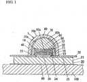
- a light emitting device 1in accordance the present embodiment comprises an LED chip 10, a circuit board 20 made of a thermally conductive material to mount the LED chip 10 thereon, a frame 40 surrounding the LED chip 10 on the surface of the circuit board 20, an encapsulation member 50 which is elastic and is made of a translucent material (transparent resin) filled within the frame 40 to encapsulate the LED chip 10 and bonding wires 14 connected to the LED chip 10, a lens 60 superimposed on the encapsulation member 50, and a dome-shaped color conversion member 70 which is a molded member molded from a transparent material mixed with a fluorescent material and disposed on the circuit board 20 to cover the lens 60.
- the light emitting device 1 of the present embodimentis adapted in use, for example, as a light source for an illumination appliance, and is mounted on a metal body 100 of the appliance (e.g. made of a metal with a high thermal conductivity such as Al or Cu) through a dielectric layer 90 made of, for example, a green sheet.
- a thermal resistance from the LED chip 10 to the metal body 100can becomes less to thereby improve heat-dissipation capability. Further, since a temperature rise at a junction of the LED chip can be restricted, an input power can be increased to increase an output power.
- a plurality of the light emitting devices 1may be mounted on the metal body 100 of the appliance in order to obtain an intended output light power, with the light emitting devices being connected in series or parallel with each other.
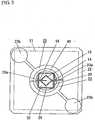
- the circuit board 20includes a metal plate 21 and a dielectric substrate 22 made of a glass epoxy board and superimposed on the metal plate 21.
- the dielectric substrate 22is provided on its surface opposite of the metal plate 21 with a pair of lead patterns for electrical connection respectively with electrodes (not shown) of the LED chip 10, and is formed with a through-hole 24 through which a sub-mount member 30 mentioned hereinafter is exposed.
- the metal plate 21is made of Cu in the present embodiment, it may be made of another metal having a relatively high thermal conductivity, such as Al. Further, in the embodiment, the metal plate 21 is made of a thermally conductive material to define itself as a heat-conductive plate on which the LED chip 10 is mounted.
- the metal plate 21is secured to the dielectric substrate 22 by means of an adhesive member 25 made of an dielectric adhesive sheet film.
- an adhesive member 25made of an dielectric adhesive sheet film.
- the adhesive member 25it is equally possible to provide a coupling metal layer on the dielectric substrate adjacent to the metal plate 21 in order to secure the dielectric substrate 22 to the metal plate 21 by means of the coupling metal layer.
- Each of the lead patterns 23is realized by a laminate composed of a Ni-layer and an Au-layer, and defines an inner lead part 23a by its portion located inwardly of the frame 40, and an outer lead part 23b by its portion not covered by a color transformation member 70.
- Each of lead patterns 23is not limited to the laminate of N-layer and Au-layer, and may be realized by a laminate of Cu-layer, Ni-layer, and Ag-layer.
- the LED chip 10is a blue LED chip based on GaN radiating blue light and is configure to have a square planar shape.
- the LED chip 10includes an electrically conductive substrate as an epitaxial substrate, which is a n-type SiC substrate having a lattice constant and a crystalline structure closer to those of GaN than sapphire, and being electrically conductive.
- an electrically conductive substrateas an epitaxial substrate, which is a n-type SiC substrate having a lattice constant and a crystalline structure closer to those of GaN than sapphire, and being electrically conductive.
- a light emitting part 12which is made of GaN based semiconductor material and is obtained by an epitaxial growth (.e.g, MOVPE process) to have a laminated structure, e.g. double-hetero structure.
- a cathode electrode(n-type electrode) (not shown) is formed on the back side of the electrically-conductive substrate 11 as an electrode on the side of the cathode.
- An anode electrode(p-type electrode) (not shown) is formed on the surface (a frontmost surface of the principal surface of the conductive substrate 11 ) of the light emitting part 12 as an electrode on the side of the anode.
- the LED chip 10has the anode electrode on its one surface, and has the cathode electrode on the opposite surface.
- the cathode electrode and the anode electrodeeach composed of the laminate of Ni-layer and Au-layer
- the cathode electrode as well as the anode electrodeare not limited to the specific materials, and may be made of a material (e.g. Al) exhibiting a good ohmic property.
- the present embodimentillustrates that the LED chip 10 is mounted on the metal plate 21 with the light emitting part 12 of the LED chip 10 being spaced further away from the metal plate 21 than from the electrically conductive substrate 11.
- the close disposition of the light emitting part 12 to the metal plate 21does not increase the optical extraction loss because of that the electrically-conductive substrate 11 and the light emitting part 12 have the refractive index of the same level in the present embodiment.
- the LED chip 10is mounted on the metal plate 21 through the sub-mount member 30 within the through-hole 24.
- the sub-mount member 30is shaped into a rectangular plate (a square planar plate in this instance) which is dimensioned to be larger than the LED chip 10 and smaller than the metal plate 21 and relieves a stress applied to the LED chip 10 due to a difference in linear thermal expansion coefficient between the LED chip 10 and the metal plate 21. Further, in addition to relieving the above-mentioned stress, the sub-mount member 30 has a thermal conducting function of conducting the heat generated at the LED chip 10 to the metal plate 21 over an area wider than the size of the chip size of the LED chip 10. The heat generated at the LED chip 10 conducts to the metal plate 21 through the sub-mount member 30 without through the dielectric substrate 22.
- the material of the sub-mount member 30is not limited to AIN, and may be selected to have the linear thermal expansion coefficient relatively close to that of electrically-conductive substrate 11 made of 6H-SiC, and relatively high thermal conductivity, e.g. composite SiC, Si, or and the like.
- the sub-mount member 30includes a conductive pattern 31 connected to above-mentioned cathode electrode on the surface of the LED chip 10, and also includes a reflecting film 32 (e.g. laminate of Ni film and Ag film, Al film, and the like) reflecting a light radiated from the side face of the LED chip 10.
- the sub-mount member 30includes the reflection film 32 disposed around a juncture of the LED chip 10 to reflect the light radiated from the side face of the LED chip 10.
- a thickness of the sub-mount member 30is selected such that the reflecting film 32 has its surface spaced from the metal plate 21 (heat conductive plate) by a greater distance than from the dielectric substrate 22.
- the sub-mount member 30By selecting a thickness of the sub-mount member 30 in above-mentioned manner in addition to disposing the reflecting film 32 on the sub-mount member 30, it is capable of preventing the absorption of the light radiated from the side wall of the LED chip 10 in a surface of the sub-mount member 30 and a side wall of the dielectric substrate 22, and also the leakage through a juncture between the color conversion member 70 and the dielectric substrate 22, thereby improving optical extraction efficiency. Moreover, it is possible to reduce color shading by preventing the leakage of the light radiated from the side wall of the LED chip 10 through above-mentioned juncture between the color conversion member 70 and the dielectric substrate 22.
- the LED chip 10has the cathode electrode electrically connected to one of the lead patterns 23 through the conductive pattern 31 and through the bonding wire 14 (e.g. gold thin wire, aluminum thin wire), and has the anode electrode electrically connected to the other lead pattern 23 through the bonding wire 14.
- the bonding wire 14e.g. gold thin wire, aluminum thin wire
- the LED chip 10is disposed centrally of the sub-mount member 30 in such a manner that the planar sides of the LED chip 10 cross with corresponding diagonals of the sub-mount member 30.
- the LED chip 10has its center axis substantially aligned with that of the sub-mount member 30 along the thickness thereof with each planar side of the LED chip 10 intersecting the corresponding one of the diagonals at an angle of about 45°. With such arrangement, it is possible to reflect the light radiated from each side wall of the LED chip 10 effectively at the reflecting film 32.
- the LED chip 10is disposed centrally of the sub-mount member 30 in such a manner that the planar sides of the LED chip 10 cross with corresponding diagonals of the sub-mount member 30.
- the LED chip 10has its center axis substantially aligned with that of the sub-mount member 30 along the thickness thereof, while each planar side of the LED chip 10 intersects the corresponding one of the diagonals at an angle of about 45°. With such arrangement, it is possible to reflect the light radiated from each side wall of the LED chip 10 effectively at the reflecting film 32.
- the light emitting device of the present embodimentis configured such that each of the bonding wires 14 electrically coupled to the LED chip 10 extends in a direction along a diagonal of the LED chip 10 so as to reduce a chance of blocking off the light radiated from each side of the LED chip 10. Consequently, it is possible to restrain lowering of the optical extraction efficiency by the presence of the bonding wire 14.
- the LED chip 10 and the sub-mount member 30can be joined by a solder such as SnPb, AuSn, SnAgCu, or a silver paste, they are preferably joined by use of a lead free solder such as AuSn, SnAgCu.
- a silicone resinis used for the encapsulation member 50 as a transparent material.
- the encapsulation membermay be made of an acrylic resin instead of the silicone resin.
- the frame 40is molded from a transparent resin into a cylindrical shape.
- the frame 40is provided on the dielectric substrate 22 to surround the LED chip 10 and the sub-mount member 30.
- the embodimentillustrates that the frame 40 is made of a silicone resin, namely the transparent material having a linear thermal expansion coefficient nearly equal to that of the encapsulation member 50.
- the acrylic resinis used for the encapsulation member 50 instead of the silicone resin, it is desirable to mold the frame 40 by use of an acrylic resin.
- the embodimentdenotes that the encapsulation member 50 is defined by the transparent material which is filled within the frame and heat-cured after the frame 40 is adhered to the circuit board 20.
- the size of the encapsulation member 50can be determined by the frame 40. Furthermore, in comparison with a conventional case where the frame is made of a metallic material, the frame 40 molded from a transparent material can reduce a difference in linear thermal expansion coefficient between the frame 40 and the encapsulation member 50, thereby restraining the generation of voids in low temperature condition during a heat cycle test. Moreover, the frame 40 can reduce a light reflection loss and therefore improve the light output efficiency.
- the lens 60is configured as a double-convex lens having a convex light incident surface 60a opposing the encapsulation 50 and a convex light emitting surface 60b.
- the lens 60is molded from a silicone resin to have the same refractive index as the encapsulation 50.
- the lens 60is not limited to the silicone resin mold but may be molded from acrylic resin.
- the light emitting surface 60b of the lensis bulged outwardly so as not to cause the total internal reflection of the light reaching the light incident surface 60a at an interface between the light emitting surface 60b and the above-mentioned air layer 80. Further, the lens 60 is disposed to have its optical axis aligned with a center line of the light emitting part 12 extending through the LED chip 10 in a thickness direction thereof.
- the color conversion member 70is molded from a mixture of a transparent material, e.g. silicone resin and a particulate yellowish fluorescent material which is excited by a blue light emitted from the LED chip 10 and passing through the encapsulation 50 to radiate a broad yellowish white light.
- the light emitted from the side wall of the LED chip 10propagates through the encapsulation 50 and the air layer 80 to reach the color conversion member 70, exciting the fluorescent material of the cooler conversion member 70 or passing through the color conversion member 70 without colliding with the fluorescent material.
- the light emitting device 1 of the present embodimentcan give a white light as a combination of the blue light emitted from the LED chip 10 and the light emitted from the yellowish fluorescent material.
- the color conversion member 70has its inner surface 70a shaped in conformity with the light emitting surface 60b of the lens 60, leaving an uniform tangential distance between the light emitting surface 60b and the inner surface 70a of the color conversion member 70 over the entire surface of the light emitting surface 60b. Further, the color conversion member 70 is shaped to have a uniform thickness along the tangential direction.
- the color conversion member 70is secured at the perimeter of its opening to the dielectric substrate 22 by means of a bond (not shown) provided by, for example, an adhesive (e.g. silicone resin, epoxy resin), to leave the air layer 80 confined between the color conversion member 70 and the light emitting surface 60b of the lens and also the frame 40.
- an adhesivee.g. silicone resin, epoxy resin
- the presence of the air layer 80reduces a possibility of the contact between the lens 60 and the color conversion member 70 when the latter is deformed as being subjected to an external force. Therefore, a stress developed at the color conversion member 70 due to the external force can be prevented from being transmitted to the LED chip 10 as well as the bonding wires 14, which reduces degradation of luminescent performance of the LED chip 10 as well as breaking of the bonding wires 14, and therefore giving improved reliability.
- the LED chip 10can be protected from moisture in the external atmosphere. Furthermore, since there is no need to make the color conversion member 70 in an intimate contact to the lens 60 and the frame 40, it is possible to prevent a lowering of yield which would be otherwise caused by dimensional accuracy or positioning accuracy concerned with the color conversion member 70. Since the color conversion member 70 is assembled last, it is possible to reduce color variance simply by selecting the color conversion member 70 in which the mixing ratio of the fluorescent material to the transparent material is adjusted in relation to the wavelength of the light from the LED chip 10.
- the air layer 80 between the color conversion member 70 and the lens 60it becomes possible to reduce an amount of the light being diffused back into the lens 60 from the color conversion member 70, a fraction of the light emitted from the LED chip 10 to be incident upon the color conversion member 70 through the encapsulation member 50 and the lens 60 followed by being scattered by the yellowish fluorescent particles in the color conversion member 70. Consequently, an optical extraction efficiency of the whole device can be improved.
- the optical axis of the color conversion member 70is aligned with the optical axis of the LED chip so that a blue light radiated from the LED chip 10 is uniformly scattered in every direction from the central point P of the color conversion member 70 along its optical axis.
- the color conversion member 70develops an escape cone ECa having a spread angle 2 ⁇ a as well as an escape cone ECb having a spread angle 2 ⁇ b, respectively on inside and outside of the color conversion member 70.
- only 13% of the blue light scattered at point Preflects back to the lens 60 with the provision of the air layer 80 between the color conversion member 70 and the lens 60, while as much as about 50% of the blue light reflects without the air layer. Accordingly, the optical extraction efficiency can be improved and a deterioration of the encapsulation member 50 by blue light can be restrained. It is desirable to use the color conversion member 70 of an increased thickness for reducing the blue light directed through the escape cone ECa.
- the transparent material used for the color conversion member 70is not limited to the silicone resin, but may include, for example, an acrylic resin, an epoxy resin, glass.
- the fluorescent material mixed to the transparent material for the color conversion member 70is not limited to the yellowish fluorescent material, and may be replaced with a mixture of a reddish fluorescent material and a greenish fluorescent material which gives a white light.
- the above embodimentillustrates the use of the SiC substrate as the electrically conductive substrate 11 carrying the LED chip 10 which is the blue LED chip giving a blue luminescence, however, the substrate 11 may be alternatively made of GaN substrate. With the use of the SiC- and GaN-substrate, the epitaxial substrate has a higher thermal conductivity to reduce the thermal resistance as compared to the dielectric sapphire substrate.
- the LED chip 10may be configured to emit the red or green light, rather than the blue light.
- the material of the light emitting part 12 of the LED chip 10is not limited to the GaN-based semiconductor composite material, but may include GaAs-based semiconductor composite material, or GaP-based semiconductor composite material.
- the electrically-conductive substrate 11is not limited to the SiC substrate, but may be selected from GaAs substrate, a GaP substrate, and the like in compatible with the material of the light emitting part 12.
- the light emitting device 1 of the present embodimentis configured to include the reflecting film 32 on the sub-mount member 30 and also to select the thickness of the sub-mount member such that the surface of the reflecting film 32 is spaced further away from the metal plate (heat conductive plate) 21 than the surface of the dielectric substrate 22.
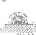
- the light emitted from the side wall of the LED chip 10can be prevented from being absorbed in the surface of the sub-mount member 30 or in the side wall of the dielectric substrate, and also from being leaked through the juncture between the color conversion member 70 and the dielectric substrate 22, thereby improving the optical output efficiency. With the improved output efficiency, the light output is improved. It is noted that, although the present embodiment illustrates the light emitting device 1 with the frame 40 made of the transparent resin, the frame may be omitted, as shown in FIG. 6 .
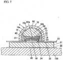
- the light emitting device 1 of the present embodimentmay utilizes a frame 40' made of a conventional metal instead of the frame 40 made of the transparent resin.
- the sub-mount member 30is selected to have a thickness such that the reflecting film 32 has its surface spaced from the metal plate 21 (heat conductive plate) by a greater distance than from the dielectric substrate 22.
Landscapes
- Led Device Packages (AREA)
Description
- The invention relates to a light emitting device using a LED (Light Emitting Diode) chip.
- Japanese Unexamined Patent Application Publication No.
2001-85748 2001-148514 Patent document 1 and 2 is shaped to have an opening area which becomes greater as it is spaced away from the circuit board and is finished to have a mirror interior face which serves as a reflector reflecting a light emitted from the LED chip. However, the above light emitting device is found unsatisfactory in extracting the light efficiently because of that the light radiated from the side faces of the LED chip is absorbed in the circuit board, or leaked through a junction between the frame and the circuit board. US 6,936,855 B1 discloses a light emitting device according to the preamble ofclaim 1, which includes a heat spreader, dielectric material above the heat spreader, and a bendable electrical connection layer disposed above the heat spreaders and electrically insulated from these heat spreaders by the dielectric material.EP 1 030 377 A2- The aforesaid problems are solved by a light emitting device according to
claim 1 which defines the present invention. Claims 2 to 5 refer to specifically advantageous realisations of the subject matter ofclaim 1. - In view of the above problem, the present invention has been accomplished and has an object of providing a light emitting device which is capable of improving its optical output.
- The light emitting device in accordance with the present invention comprises the LED chip, a heat conductive plate which is made of a heat conductive material to mount thereon the LED chip, a sub-mount member of being configured to be shaped into a planar plate which is dimensioned to be larger than the LED chip and smaller than the heat conductive plate, a dielectric substrate stacked on the heat conductive member, an encapsulation member being made of a transparent and elastic material to encapsulate the LED chip, and a lens superposed on the encapsulation member. The sub-mount member is disposed between the LED chip and the heat conductive plate to relieve a stress applied to the LED chip due to a difference in linear thermal expansion coefficient between the LED chip and the heat conductive plate. Also, the dielectric substrate is provided on a surface opposite of the heat conductive plate with a pair of lead patterns for electrical connection respectively with electrodes of the LED chip. Further, the dielectric substrate is formed with a through-hole through which the sub-mount member is exposed. The sub-mount member includes a reflection film disposed around a junction of the LED chip to reflect a light emitted from a side wall of the LED chip, and is selected to have a thickness such that the reflecting film has its surface spaced from the heat conductive plate by a greater distance than the dielectric substrate.
- Since the light emitting device of the invention is configured to include the sub-mount member with a reflection film having such a thickness that the surface of the reflecting film is spaced from the head conductive plate by a greater distance than from the dielectric substrate, it is capable of preventing the absorption of the light radiated from the side wall of the LED chip in a surface or a side wall of the dielectric substrate, thereby improving optical extraction efficiency with an associated improvement of the optical output.
- Generally, a color conversion member is deposited on a surface of the dielectric substrate to convert a color of a light radiated from the LED chip or the metal frame which reflects a light of the LED chip. By selecting the thickness such that the reflecting film has its surface spaced from the heat conductive plate by a greater distance than from the dielectric substrate, it becomes possible to prevent the light from leaking through a juncture between the above color conversion member and the dielectric substrate even if the above color conversion member is disposed on the surface of the dielectric substrate.
- Consequently, it becomes possible to improve the optical extraction efficiency, and reduce color shading too.
- Preferably, both of the LED chip and the sub-mount member are each configured to have a square planar shape, and the LED chip is disposed centrally of the sub-mount member in such a manner that planar sides of the LED chip crosses respectively with corresponding ones diagonals of the sub-mount member.
- In this case, the reflection film can effectively reflect a light radiated from each side walls of the LED chip towards the sub-mount member. Preferably, the light emitting device, further, includes the frame provided on a surface of the dielectric substrate to surround the sub-mount member and said the LED chip, and the encapsulation member is defined by a transparent material filled within the frame. The frame is molded from a transparent resin.
- The frame may be configured to determine the size of the encapsulation member. Further, in comparison with a conventional case where the frame is made of a metallic material, the frame molded from a transparent material can reduce a difference in linear thermal expansion coefficient between the frame and the encapsulation member, and to restrain the generation of voids in low temperature condition during a heat cycle test. Moreover, the frame can itself reduce a light reflection loss and therefore improve the light output efficiency.
- Preferably, the LED chip is formed on its one surface with one of the electrodes and on the other surface with the other electrode. One of said electrodes adjacent to the sub-mount member is connected to one bonding wires through a conductor pattern on the sub-mount member, while the other electrode away from the sub-mount member is connected to the bonding wire which extends along one of the diagonals of the LED chip.
- In this case, the light radiated from the side wall of the LED has a less chance of being blocked by the bonding wires, whereby it is possible to reduce the lowering of the optical extraction efficiency due to the presence of the bonding wires.
- Preferably, the light emitting device is configured to further include a dome-shaped color conversion member which is disposed on the dielectric substrate to cover the lens. The color conversion member is a molded member molded from a transparent material mixed with a fluorescent material which is excited by a light emitted from the LED chip and passing through the encapsulation member to radiate a light having a color different from that of the LED chip. Further, the color conversion member is disposed to form an air layer between said color conversion member and a light emitting face of the lens.
- The provision of the color conversion member makes it possible to radiate a color different from that of the LED chip. Also, the color conversion member is disposed to form an air layer between the color conversion member and a light emitting face of the lens. When the color conversion member suffers from an external force, the air layer can restrain the color conversion member from transmitting a stress to the LED chip through the lens and the encapsulation member. Further, it becomes possible to reduce an amount of the light being directed and passing through the lens, a fraction of the light which is radiated from the LED chip to be incident upon the color conversion member through the lens and the encapsulation member and is scattered due to the fluorescent particles in the color conversion member. Consequently, an optical extraction efficiency of the whole device can be improved. Further, the LED chip can be protected from moisture in the external atmosphere. Since there is no need to make the color conversion member in an intimate contact to the lens, it becomes possible to reduce a fall of a yield caused by dimensional accuracy or positioning accuracy concerned with the color conversion member.
FIG.1 is a cross-sectional view of a light emitting device in accordance with an embodiment of the present invention;FIG.2 is a partially cutout exploded perspective view the above device;FIG. 3 is a plan view illustrating a principal part of the above device;FIG.4 is a perspective view of a sub-mount employed in the above device;FIG. 5A is an explanatory view of a principal part of the above device;FIG. 5B is an explanatory view of a principal part of the above device;FIG. 6 is a cross-section of another configuration of the above device; andFIG. 7 is a cross-section of a further configuration of the above device.- Hereinafter, the present invention will be explained in detail with reference to the attached drawings.
- As shown in
FIGS. 1 and2 , alight emitting device 1 in accordance the present embodiment comprises anLED chip 10, acircuit board 20 made of a thermally conductive material to mount theLED chip 10 thereon, aframe 40 surrounding theLED chip 10 on the surface of thecircuit board 20, anencapsulation member 50 which is elastic and is made of a translucent material (transparent resin) filled within theframe 40 to encapsulate theLED chip 10 andbonding wires 14 connected to theLED chip 10, alens 60 superimposed on theencapsulation member 50, and a dome-shapedcolor conversion member 70 which is a molded member molded from a transparent material mixed with a fluorescent material and disposed on thecircuit board 20 to cover thelens 60. Thelight emitting device 1 of the present embodiment is adapted in use, for example, as a light source for an illumination appliance, and is mounted on ametal body 100 of the appliance (e.g. made of a metal with a high thermal conductivity such as Al or Cu) through adielectric layer 90 made of, for example, a green sheet. As being mounted on themetal body 100 of the apparatus, a thermal resistance from theLED chip 10 to themetal body 100 can becomes less to thereby improve heat-dissipation capability. Further, since a temperature rise at a junction of the LED chip can be restricted, an input power can be increased to increase an output power. It is noted in this connection that, when thelight emitting devise 1 is used for the illumination appliance, a plurality of thelight emitting devices 1 may be mounted on themetal body 100 of the appliance in order to obtain an intended output light power, with the light emitting devices being connected in series or parallel with each other. - The
circuit board 20 includes ametal plate 21 and adielectric substrate 22 made of a glass epoxy board and superimposed on themetal plate 21. Thedielectric substrate 22 is provided on its surface opposite of themetal plate 21 with a pair of lead patterns for electrical connection respectively with electrodes (not shown) of theLED chip 10, and is formed with a through-hole 24 through which asub-mount member 30 mentioned hereinafter is exposed. Although, themetal plate 21 is made of Cu in the present embodiment, it may be made of another metal having a relatively high thermal conductivity, such as Al. Further, in the embodiment, themetal plate 21 is made of a thermally conductive material to define itself as a heat-conductive plate on which theLED chip 10 is mounted. Themetal plate 21 is secured to thedielectric substrate 22 by means of anadhesive member 25 made of an dielectric adhesive sheet film. Instead of theadhesive member 25, it is equally possible to provide a coupling metal layer on the dielectric substrate adjacent to themetal plate 21 in order to secure thedielectric substrate 22 to themetal plate 21 by means of the coupling metal layer. - Each of the
lead patterns 23 is realized by a laminate composed of a Ni-layer and an Au-layer, and defines an innerlead part 23a by its portion located inwardly of theframe 40, and an outerlead part 23b by its portion not covered by acolor transformation member 70. Each oflead patterns 23 is not limited to the laminate of N-layer and Au-layer, and may be realized by a laminate of Cu-layer, Ni-layer, and Ag-layer. - The
LED chip 10 is a blue LED chip based on GaN radiating blue light and is configure to have a square planar shape. TheLED chip 10 includes an electrically conductive substrate as an epitaxial substrate, which is a n-type SiC substrate having a lattice constant and a crystalline structure closer to those of GaN than sapphire, and being electrically conductive. Formed also on the main surface of the electrically-conductive substrate 11 is alight emitting part 12 which is made of GaN based semiconductor material and is obtained by an epitaxial growth (.e.g, MOVPE process) to have a laminated structure, e.g. double-hetero structure. A cathode electrode (n-type electrode) (not shown) is formed on the back side of the electrically-conductive substrate 11 as an electrode on the side of the cathode. An anode electrode (p-type electrode) (not shown) is formed on the surface (a frontmost surface of the principal surface of the conductive substrate11) of thelight emitting part 12 as an electrode on the side of the anode. In short, theLED chip 10 has the anode electrode on its one surface, and has the cathode electrode on the opposite surface. - It is noted that, although the present embodiment has the cathode electrode and the anode electrode each composed of the laminate of Ni-layer and Au-layer, the cathode electrode as well as the anode electrode are not limited to the specific materials, and may be made of a material (e.g. Al) exhibiting a good ohmic property. Further, the present embodiment illustrates that the
LED chip 10 is mounted on themetal plate 21 with thelight emitting part 12 of theLED chip 10 being spaced further away from themetal plate 21 than from the electricallyconductive substrate 11. However, it is equally possible to mount theLED chip 10 on themetal plate 21 with thelight emitting part 12 being closer to the metal plate than the electricallyconductive plate 11. Although it is desirable to space thelight emitting part 12 apart from themetal plate 21 from a viewpoint of optical extraction efficiency, the close disposition of thelight emitting part 12 to themetal plate 21 does not increase the optical extraction loss because of that the electrically-conductive substrate 11 and thelight emitting part 12 have the refractive index of the same level in the present embodiment. - The
LED chip 10 is mounted on themetal plate 21 through thesub-mount member 30 within the through-hole 24. Thesub-mount member 30 is shaped into a rectangular plate (a square planar plate in this instance) which is dimensioned to be larger than theLED chip 10 and smaller than themetal plate 21 and relieves a stress applied to theLED chip 10 due to a difference in linear thermal expansion coefficient between theLED chip 10 and themetal plate 21. Further, in addition to relieving the above-mentioned stress, thesub-mount member 30 has a thermal conducting function of conducting the heat generated at theLED chip 10 to themetal plate 21 over an area wider than the size of the chip size of theLED chip 10. The heat generated at theLED chip 10 conducts to themetal plate 21 through thesub-mount member 30 without through thedielectric substrate 22. - It is noted in this connection that, although AIN is adopted as a material of the
sub-mount member 30 because of having both relatively high thermal conductivity and insulating performance, the material of thesub-mount member 30 is not limited to AIN, and may be selected to have the linear thermal expansion coefficient relatively close to that of electrically-conductive substrate 11 made of 6H-SiC, and relatively high thermal conductivity, e.g. composite SiC, Si, or and the like. - As shown in
FIG. 4 , thesub-mount member 30 includes aconductive pattern 31 connected to above-mentioned cathode electrode on the surface of theLED chip 10, and also includes a reflecting film32 (e.g. laminate of Ni film and Ag film, Al film, and the like) reflecting a light radiated from the side face of theLED chip 10. In short, thesub-mount member 30 includes thereflection film 32 disposed around a juncture of theLED chip 10 to reflect the light radiated from the side face of theLED chip 10. Furthermore, a thickness of thesub-mount member 30 is selected such that the reflectingfilm 32 has its surface spaced from the metal plate21 (heat conductive plate) by a greater distance than from thedielectric substrate 22. - By selecting a thickness of the
sub-mount member 30 in above-mentioned manner in addition to disposing the reflectingfilm 32 on thesub-mount member 30, it is capable of preventing the absorption of the light radiated from the side wall of theLED chip 10 in a surface of thesub-mount member 30 and a side wall of thedielectric substrate 22, and also the leakage through a juncture between thecolor conversion member 70 and thedielectric substrate 22, thereby improving optical extraction efficiency. Moreover, it is possible to reduce color shading by preventing the leakage of the light radiated from the side wall of theLED chip 10 through above-mentioned juncture between thecolor conversion member 70 and thedielectric substrate 22. - The
LED chip 10 has the cathode electrode electrically connected to one of thelead patterns 23 through theconductive pattern 31 and through the bonding wire14 (e.g. gold thin wire, aluminum thin wire), and has the anode electrode electrically connected to theother lead pattern 23 through thebonding wire 14. - The
LED chip 10 is disposed centrally of thesub-mount member 30 in such a manner that the planar sides of theLED chip 10 cross with corresponding diagonals of thesub-mount member 30. In the present embodiment, theLED chip 10 has its center axis substantially aligned with that of thesub-mount member 30 along the thickness thereof with each planar side of theLED chip 10 intersecting the corresponding one of the diagonals at an angle of about 45°. With such arrangement, it is possible to reflect the light radiated from each side wall of theLED chip 10 effectively at the reflectingfilm 32. TheLED chip 10 is disposed centrally of thesub-mount member 30 in such a manner that the planar sides of theLED chip 10 cross with corresponding diagonals of thesub-mount member 30. - In the present embodiment, the
LED chip 10 has its center axis substantially aligned with that of thesub-mount member 30 along the thickness thereof, while each planar side of theLED chip 10 intersects the corresponding one of the diagonals at an angle of about 45°. With such arrangement, it is possible to reflect the light radiated from each side wall of theLED chip 10 effectively at the reflectingfilm 32. - As shown in
FIG.3 , the light emitting device of the present embodiment is configured such that each of thebonding wires 14 electrically coupled to theLED chip 10 extends in a direction along a diagonal of theLED chip 10 so as to reduce a chance of blocking off the light radiated from each side of theLED chip 10. Consequently, it is possible to restrain lowering of the optical extraction efficiency by the presence of thebonding wire 14. - Although the
LED chip 10 and thesub-mount member 30 can be joined by a solder such as SnPb, AuSn, SnAgCu, or a silver paste, they are preferably joined by use of a lead free solder such as AuSn, SnAgCu. - A silicone resin is used for the
encapsulation member 50 as a transparent material. However, the encapsulation member may be made of an acrylic resin instead of the silicone resin. - The
frame 40 is molded from a transparent resin into a cylindrical shape. Theframe 40 is provided on thedielectric substrate 22 to surround theLED chip 10 and thesub-mount member 30. The embodiment illustrates that theframe 40 is made of a silicone resin, namely the transparent material having a linear thermal expansion coefficient nearly equal to that of theencapsulation member 50. When the acrylic resin is used for theencapsulation member 50 instead of the silicone resin, it is desirable to mold theframe 40 by use of an acrylic resin. The embodiment denotes that theencapsulation member 50 is defined by the transparent material which is filled within the frame and heat-cured after theframe 40 is adhered to thecircuit board 20. - With the provision of the frame, the size of the
encapsulation member 50 can be determined by theframe 40. Furthermore, in comparison with a conventional case where the frame is made of a metallic material, theframe 40 molded from a transparent material can reduce a difference in linear thermal expansion coefficient between theframe 40 and theencapsulation member 50, thereby restraining the generation of voids in low temperature condition during a heat cycle test. Moreover, theframe 40 can reduce a light reflection loss and therefore improve the light output efficiency. - The
lens 60 is configured as a double-convex lens having a convexlight incident surface 60a opposing theencapsulation 50 and a convexlight emitting surface 60b. Thelens 60 is molded from a silicone resin to have the same refractive index as theencapsulation 50. Thelens 60 is not limited to the silicone resin mold but may be molded from acrylic resin. Thelight emitting surface 60b of the lens is bulged outwardly so as not to cause the total internal reflection of the light reaching thelight incident surface 60a at an interface between thelight emitting surface 60b and the above-mentionedair layer 80. Further, thelens 60 is disposed to have its optical axis aligned with a center line of thelight emitting part 12 extending through theLED chip 10 in a thickness direction thereof. - The
color conversion member 70 is molded from a mixture of a transparent material, e.g. silicone resin and a particulate yellowish fluorescent material which is excited by a blue light emitted from theLED chip 10 and passing through theencapsulation 50 to radiate a broad yellowish white light. The light emitted from the side wall of theLED chip 10 propagates through theencapsulation 50 and theair layer 80 to reach thecolor conversion member 70, exciting the fluorescent material of thecooler conversion member 70 or passing through thecolor conversion member 70 without colliding with the fluorescent material. Thelight emitting device 1 of the present embodiment can give a white light as a combination of the blue light emitted from theLED chip 10 and the light emitted from the yellowish fluorescent material. - The
color conversion member 70 has itsinner surface 70a shaped in conformity with thelight emitting surface 60b of thelens 60, leaving an uniform tangential distance between thelight emitting surface 60b and theinner surface 70a of thecolor conversion member 70 over the entire surface of thelight emitting surface 60b. Further, thecolor conversion member 70 is shaped to have a uniform thickness along the tangential direction. - The
color conversion member 70 is secured at the perimeter of its opening to thedielectric substrate 22 by means of a bond (not shown) provided by, for example, an adhesive (e.g. silicone resin, epoxy resin), to leave theair layer 80 confined between thecolor conversion member 70 and thelight emitting surface 60b of the lens and also theframe 40. The presence of theair layer 80 reduces a possibility of the contact between thelens 60 and thecolor conversion member 70 when the latter is deformed as being subjected to an external force. Therefore, a stress developed at thecolor conversion member 70 due to the external force can be prevented from being transmitted to theLED chip 10 as well as thebonding wires 14, which reduces degradation of luminescent performance of theLED chip 10 as well as breaking of thebonding wires 14, and therefore giving improved reliability. Further, with the provision of theair layer 80 between thecolor conversion member 70 and thelens 60, theLED chip 10 can be protected from moisture in the external atmosphere. Furthermore, since there is no need to make thecolor conversion member 70 in an intimate contact to thelens 60 and theframe 40, it is possible to prevent a lowering of yield which would be otherwise caused by dimensional accuracy or positioning accuracy concerned with thecolor conversion member 70. Since thecolor conversion member 70 is assembled last, it is possible to reduce color variance simply by selecting thecolor conversion member 70 in which the mixing ratio of the fluorescent material to the transparent material is adjusted in relation to the wavelength of the light from theLED chip 10. - Also, with the provision of the
air layer 80 between thecolor conversion member 70 and thelens 60, it becomes possible to reduce an amount of the light being diffused back into thelens 60 from thecolor conversion member 70, a fraction of the light emitted from theLED chip 10 to be incident upon thecolor conversion member 70 through theencapsulation member 50 and thelens 60 followed by being scattered by the yellowish fluorescent particles in thecolor conversion member 70. Consequently, an optical extraction efficiency of the whole device can be improved. - Explanation is made with reference to
FIG.5A and FIG.5B in which the optical axis of thecolor conversion member 70 is aligned with the optical axis of the LED chip so that a blue light radiated from theLED chip 10 is uniformly scattered in every direction from the central point P of thecolor conversion member 70 along its optical axis. With regard to the light scattered at point P, thecolor conversion member 70 develops an escape cone ECa having a spread angle 2θa as well as an escape cone ECb having a spread angle 2θb, respectively on inside and outside of thecolor conversion member 70. The spread are expressed as 2θa=60°, 2θb = 98° when the total internal reflection angle φa and φb are 40°, as shown inFIG. 5A , and2 θa=76°, 2θb = 134° when the total internal reflection angle φa and φb are 50° as shown inFIG. 5B , where the total internal reflection angle φa is defined at the interface between thecolor conversion member 70 and the air layer, while the total internal reflection angle φb is defined at the interface between thecolor conversion member 70 and an air, a medium outside of thecolor conversion member 70. - The blue light scatted at point P and directed through the escape cone ECa on the inside of the color conversion member has a maximum emission efficiency η which is expressed as η=(1/4 n2) x 100 (%), where n is a refractive index of the transparent material forming the
color conversion member 70. Thus, η≒13% when the silicone resin having n=1.4 is utilized as mentioned in the above.
In other words, only 13% of the blue light scattered at point P reflects back to thelens 60 with the provision of theair layer 80 between thecolor conversion member 70 and thelens 60, while as much as about 50% of the blue light reflects without the air layer. Accordingly, the optical extraction efficiency can be improved and a deterioration of theencapsulation member 50 by blue light can be restrained. It is desirable to use thecolor conversion member 70 of an increased thickness for reducing the blue light directed through the escape cone ECa. - The transparent material used for the
color conversion member 70 is not limited to the silicone resin, but may include, for example, an acrylic resin, an epoxy resin, glass. Further, the fluorescent material mixed to the transparent material for thecolor conversion member 70 is not limited to the yellowish fluorescent material, and may be replaced with a mixture of a reddish fluorescent material and a greenish fluorescent material which gives a white light. The above embodiment illustrates the use of the SiC substrate as the electricallyconductive substrate 11 carrying theLED chip 10 which is the blue LED chip giving a blue luminescence, however, thesubstrate 11 may be alternatively made of GaN substrate. With the use of the SiC- and GaN-substrate, the epitaxial substrate has a higher thermal conductivity to reduce the thermal resistance as compared to the dielectric sapphire substrate. TheLED chip 10 may be configured to emit the red or green light, rather than the blue light. The material of thelight emitting part 12 of theLED chip 10 is not limited to the GaN-based semiconductor composite material, but may include GaAs-based semiconductor composite material, or GaP-based semiconductor composite material. - Furthermore, the electrically-
conductive substrate 11 is not limited to the SiC substrate, but may be selected from GaAs substrate, a GaP substrate, and the like in compatible with the material of thelight emitting part 12. As discussed in the above, thelight emitting device 1 of the present embodiment is configured to include the reflectingfilm 32 on thesub-mount member 30 and also to select the thickness of the sub-mount member such that the surface of the reflectingfilm 32 is spaced further away from the metal plate (heat conductive plate)21 than the surface of thedielectric substrate 22. With this configuration, the light emitted from the side wall of theLED chip 10 can be prevented from being absorbed in the surface of thesub-mount member 30 or in the side wall of the dielectric substrate, and also from being leaked through the juncture between thecolor conversion member 70 and thedielectric substrate 22, thereby improving the optical output efficiency. With the improved output efficiency, the light output is improved. It is noted that, although the present embodiment illustrates thelight emitting device 1 with theframe 40 made of the transparent resin, the frame may be omitted, as shown inFIG. 6 . - Further, the
light emitting device 1 of the present embodiment may utilizes a frame40' made of a conventional metal instead of theframe 40 made of the transparent resin. Also in this case, thesub-mount member 30 is selected to have a thickness such that the reflectingfilm 32 has its surface spaced from the metal plate21 (heat conductive plate) by a greater distance than from thedielectric substrate 22. Thus, it is also possible to make the light emitting device which is capable of preventing the absorption of the light radiated from the side wall of theLED chip 10 in a side wall of thedielectric substrate 22 and leaking of the light through the juncture between the metal frame 40' and thedielectric substrate 22, thereby improving optical extraction efficiency with an associated improvement of the optical output. - As discussed in the above, apparently many widely different embodiments may be made without departing from the present invention, which is defined in
claim 1.
Claims (5)
- A light emitting device comprising:a light emitting diode chip (10);a heat conductive plate (21) which is made of a heat conductive material and said light emitting diode chip (10) is mounted thereon;a sub-mount member (30) of a planar plate which is dimensioned to be larger than said light emitting diode chip (10) and smaller than said heat conductive plate (21), said sub-mount member (30) being disposed between said light emitting diode chip (10) and said heat conductive plate (21) and being configured to relieve a stress acting upon said light emitting diode chip (10) due to a difference in linear thermal expansion coefficient between said light emitting diode chip (10) and said heat conductive plate (21);a dielectric substrate (22) stacked on said heat conductive plate (21), said dielectric substrate (22) being provided on a surface opposite of said heat conductive plate (21) with a pair of lead patterns (23) for electrical connection respectively with electrodes of said light emitting diode chip (10), said dielectric substrate (22) being formed with a through-hole (24) through which said sub-mount member (30) is exposed;an encapsulation member (50) being made of a transparent and elastic material and configured to encapsulate said light emitting diode chip (10);a lens (60) superimposed on said encapsulation member (50); and whereinsaid sub-mount member (30) includes a reflection film (32) disposed around a juncture of said light emitting diode chip (10) and is configured to reflect a light emitted from a side face of said light emitting diode chip (10);characterized in thatsaid sub-mount member (30) is selected to have a thickness such that said reflection film (32) has its surface spaced from said heat conductive plate (21) by a greater distance than said dielectric substrate (22), and is configured to prevent absorption of said light radiated from said side face of said light emitting diode chip (10) in a surface or a side wall of said dielectric substrate (22), anda color conversion member (70) is deposited on a surface of said dielectric substrate (22) to convert a color of said light radiated from said light emitting diode chip (10) or said reflection film (32).
- The light emitting device of claim 1, wherein
both of said light emitting diode chip (10) and said sub-mount member (30) are each configured to have a square planar shape,
said light emitting diode chip (10) being disposed centrally of said sub-mount member (30) in such a manner that planar sides of said light emitting diode chip (10) crosses respectively with corresponding ones diagonals of said sub-mount member (30). - The light emitting device of claim 1, further including:a frame provided on a surface of said dielectric substrate (22) to surround said sub-mount member (30) and said light emitting diode chip (10), said encapsulation member (50) being defined by a transparent material filled inside of said frame, and said frame being molded from a transparent resin.
- The light emitting device of claim 1, wherein
said light emitting diode chip (10) is formed on its one surface with one electrode and on the other surface with another electrode (12), one of said electrodes adjacent to said sub-mount member (30) being connected to one bonding wire through a conductor pattern on said sub-mount member (30), said another electrode away from said sub-mount member (30) being connected to another bonding wire, said another bonding wire extending along one of said diagonals of said light emitting diode chip (10). - The light emitting device of claim 1, wherein said color conversion member (70) is a dome-shaped color conversion member (70) which is disposed on said dielectric substrate (22) to cover said lens (60), said color conversion member being a molded member molded from a transparent material mixed with a fluorescent material which is excited by a light emitted from said light emitting diode chip (10) and passing through said encapsulation member (50) to radiate a light having a color different from that of the light emitting diode chip (10), said color conversion member being disposed to form an air layer (80) between said color conversion member and a light emitting face of said lens (60).
Applications Claiming Priority (3)
| Application Number | Priority Date | Filing Date | Title |
|---|---|---|---|
| JP2005272832 | 2005-09-20 | ||
| JP2005334683 | 2005-11-18 | ||
| PCT/JP2005/024031WO2007034575A1 (en) | 2005-09-20 | 2005-12-28 | Light emitting device |
Publications (3)
| Publication Number | Publication Date |
|---|---|
| EP1928029A1 EP1928029A1 (en) | 2008-06-04 |
| EP1928029A4 EP1928029A4 (en) | 2011-11-23 |
| EP1928029B1true EP1928029B1 (en) | 2018-10-31 |
Family
ID=37888634
Family Applications (1)
| Application Number | Title | Priority Date | Filing Date |
|---|---|---|---|
| EP05844848.1ANot-in-forceEP1928029B1 (en) | 2005-09-20 | 2005-12-28 | Light emitting diode package |
Country Status (4)
| Country | Link |
|---|---|
| US (1) | US7956372B2 (en) |
| EP (1) | EP1928029B1 (en) |
| KR (1) | KR100985452B1 (en) |
| WO (1) | WO2007034575A1 (en) |
Families Citing this family (62)
| Publication number | Priority date | Publication date | Assignee | Title |
|---|---|---|---|---|
| US8545629B2 (en) | 2001-12-24 | 2013-10-01 | Crystal Is, Inc. | Method and apparatus for producing large, single-crystals of aluminum nitride |
| JP3992059B2 (en)* | 2005-11-21 | 2007-10-17 | 松下電工株式会社 | Method for manufacturing light emitting device |
| JP4013077B2 (en) | 2005-11-21 | 2007-11-28 | 松下電工株式会社 | Light emitting device and manufacturing method thereof |
| JP5281408B2 (en) | 2005-12-02 | 2013-09-04 | クリスタル・イズ,インコーポレイテッド | Doped aluminum nitride crystal and method for producing the same |
| US9034103B2 (en)* | 2006-03-30 | 2015-05-19 | Crystal Is, Inc. | Aluminum nitride bulk crystals having high transparency to ultraviolet light and methods of forming them |
| US8323406B2 (en) | 2007-01-17 | 2012-12-04 | Crystal Is, Inc. | Defect reduction in seeded aluminum nitride crystal growth |
| US9771666B2 (en) | 2007-01-17 | 2017-09-26 | Crystal Is, Inc. | Defect reduction in seeded aluminum nitride crystal growth |
| US8080833B2 (en) | 2007-01-26 | 2011-12-20 | Crystal Is, Inc. | Thick pseudomorphic nitride epitaxial layers |
| JP5006102B2 (en) | 2007-05-18 | 2012-08-22 | 株式会社東芝 | Light emitting device and manufacturing method thereof |
| TW200915597A (en)* | 2007-09-17 | 2009-04-01 | Everlight Electronics Co Ltd | Light emitting diode device |
| JP2010074117A (en)* | 2007-12-07 | 2010-04-02 | Panasonic Electric Works Co Ltd | Light emitting device |
| US20110163348A1 (en)* | 2008-03-25 | 2011-07-07 | Bridge Semiconductor Corporation | Semiconductor chip assembly with bump/base heat spreader and inverted cavity in bump |
| US20100072511A1 (en)* | 2008-03-25 | 2010-03-25 | Lin Charles W C | Semiconductor chip assembly with copper/aluminum post/base heat spreader |
| US8531024B2 (en)* | 2008-03-25 | 2013-09-10 | Bridge Semiconductor Corporation | Semiconductor chip assembly with post/base heat spreader and multilevel conductive trace |
| US20110156090A1 (en)* | 2008-03-25 | 2011-06-30 | Lin Charles W C | Semiconductor chip assembly with post/base/post heat spreader and asymmetric posts |
| US8232576B1 (en) | 2008-03-25 | 2012-07-31 | Bridge Semiconductor Corporation | Semiconductor chip assembly with post/base heat spreader and ceramic block in post |
| US8324723B2 (en)* | 2008-03-25 | 2012-12-04 | Bridge Semiconductor Corporation | Semiconductor chip assembly with bump/base heat spreader and dual-angle cavity in bump |
| US8212279B2 (en) | 2008-03-25 | 2012-07-03 | Bridge Semiconductor Corporation | Semiconductor chip assembly with post/base heat spreader, signal post and cavity |
| US8314438B2 (en)* | 2008-03-25 | 2012-11-20 | Bridge Semiconductor Corporation | Semiconductor chip assembly with bump/base heat spreader and cavity in bump |
| US8354688B2 (en) | 2008-03-25 | 2013-01-15 | Bridge Semiconductor Corporation | Semiconductor chip assembly with bump/base/ledge heat spreader, dual adhesives and cavity in bump |
| US8288792B2 (en)* | 2008-03-25 | 2012-10-16 | Bridge Semiconductor Corporation | Semiconductor chip assembly with post/base/post heat spreader |
| US8203167B2 (en) | 2008-03-25 | 2012-06-19 | Bridge Semiconductor Corporation | Semiconductor chip assembly with post/base heat spreader and adhesive between base and terminal |
| US20090284932A1 (en)* | 2008-03-25 | 2009-11-19 | Bridge Semiconductor Corporation | Thermally Enhanced Package with Embedded Metal Slug and Patterned Circuitry |
| US9018667B2 (en)* | 2008-03-25 | 2015-04-28 | Bridge Semiconductor Corporation | Semiconductor chip assembly with post/base heat spreader and dual adhesives |
| US8148747B2 (en)* | 2008-03-25 | 2012-04-03 | Bridge Semiconductor Corporation | Semiconductor chip assembly with post/base/cap heat spreader |
| US20100181594A1 (en) | 2008-03-25 | 2010-07-22 | Lin Charles W C | Semiconductor chip assembly with post/base heat spreader and cavity over post |
| US8329510B2 (en) | 2008-03-25 | 2012-12-11 | Bridge Semiconductor Corporation | Method of making a semiconductor chip assembly with a post/base heat spreader with an ESD protection layer |
| US8415703B2 (en) | 2008-03-25 | 2013-04-09 | Bridge Semiconductor Corporation | Semiconductor chip assembly with post/base/flange heat spreader and cavity in flange |
| US8110446B2 (en)* | 2008-03-25 | 2012-02-07 | Bridge Semiconductor Corporation | Method of making a semiconductor chip assembly with a post/base heat spreader and a conductive trace |
| US8067784B2 (en)* | 2008-03-25 | 2011-11-29 | Bridge Semiconductor Corporation | Semiconductor chip assembly with post/base heat spreader and substrate |
| US8193556B2 (en)* | 2008-03-25 | 2012-06-05 | Bridge Semiconductor Corporation | Semiconductor chip assembly with post/base heat spreader and cavity in post |
| US8129742B2 (en) | 2008-03-25 | 2012-03-06 | Bridge Semiconductor Corporation | Semiconductor chip assembly with post/base heat spreader and plated through-hole |
| US8207553B2 (en)* | 2008-03-25 | 2012-06-26 | Bridge Semiconductor Corporation | Semiconductor chip assembly with base heat spreader and cavity in base |
| US20100052005A1 (en)* | 2008-03-25 | 2010-03-04 | Lin Charles W C | Semiconductor chip assembly with post/base heat spreader and conductive trace |
| US8269336B2 (en)* | 2008-03-25 | 2012-09-18 | Bridge Semiconductor Corporation | Semiconductor chip assembly with post/base heat spreader and signal post |
| US20110278638A1 (en) | 2008-03-25 | 2011-11-17 | Lin Charles W C | Semiconductor chip assembly with post/dielectric/post heat spreader |
| US8310043B2 (en) | 2008-03-25 | 2012-11-13 | Bridge Semiconductor Corporation | Semiconductor chip assembly with post/base heat spreader with ESD protection layer |
| US8378372B2 (en)* | 2008-03-25 | 2013-02-19 | Bridge Semiconductor Corporation | Semiconductor chip assembly with post/base heat spreader and horizontal signal routing |
| US8525214B2 (en)* | 2008-03-25 | 2013-09-03 | Bridge Semiconductor Corporation | Semiconductor chip assembly with post/base heat spreader with thermal via |
| JP5665160B2 (en)* | 2008-03-26 | 2015-02-04 | パナソニックIpマネジメント株式会社 | Light emitting device and lighting apparatus |
| KR100976528B1 (en)* | 2008-08-14 | 2010-08-17 | 주식회사 루미맥스테크놀러지 | Anti-glare LED lighting device |
| GB2466633A (en)* | 2008-12-12 | 2010-07-07 | Glory Science Co Ltd | Method of manufacturing a light emitting unit |
| TWI449221B (en)* | 2009-01-16 | 2014-08-11 | Everlight Electronics Co Ltd | Light-emitting diode package structure and manufacturing method thereof |
| DE202009018419U1 (en) | 2009-03-09 | 2011-08-17 | Tridonic Jennersdorf Gmbh | LED module with improved light output |
| US8324653B1 (en) | 2009-08-06 | 2012-12-04 | Bridge Semiconductor Corporation | Semiconductor chip assembly with ceramic/metal substrate |
| US8486761B2 (en) | 2010-03-25 | 2013-07-16 | Koninklijke Philips Electronics N.V. | Hybrid combination of substrate and carrier mounted light emitting devices |
| US8319247B2 (en)* | 2010-03-25 | 2012-11-27 | Koninklijke Philips Electronics N.V. | Carrier for a light emitting device |
| WO2012006128A2 (en)* | 2010-06-28 | 2012-01-12 | Axlen Technologies, Inc. | High brightness illumination devices using wavelength conversion materials |
| CN105951177B (en) | 2010-06-30 | 2018-11-02 | 晶体公司 | Use the growth for the bulk aluminum nitride single crystal that thermal gradient controls |
| US8598463B2 (en)* | 2010-08-05 | 2013-12-03 | Unimicron Technology Corp. | Circuit board and manufacturing method thereof |
| US8962359B2 (en) | 2011-07-19 | 2015-02-24 | Crystal Is, Inc. | Photon extraction from nitride ultraviolet light-emitting devices |
| EP2634480B1 (en) | 2011-11-21 | 2016-09-28 | Panasonic Intellectual Property Management Co., Ltd. | Light emitting apparatus and illuminating apparatus |
| CN103000785A (en)* | 2012-11-05 | 2013-03-27 | 何忠亮 | LED luminous structure and method for manufacturing same |
| DE102013201327A1 (en)* | 2013-01-28 | 2014-07-31 | Osram Gmbh | Printed circuit board, optoelectronic component and arrangement of optoelectronic components |
| US20150280057A1 (en) | 2013-03-15 | 2015-10-01 | James R. Grandusky | Methods of forming planar contacts to pseudomorphic electronic and optoelectronic devices |
| JP6476567B2 (en) | 2013-03-29 | 2019-03-06 | 日亜化学工業株式会社 | Light emitting device |
| TWI510741B (en)* | 2013-05-27 | 2015-12-01 | Genesis Photonics Inc | Illuminating device |
| US9196584B2 (en) | 2013-07-12 | 2015-11-24 | Panasonic Intellectual Property Management Co., Ltd. | Light-emitting device and lighting apparatus using the same |
| CN107079578A (en)* | 2014-09-24 | 2017-08-18 | Hiq太阳能股份有限公司 | Transistor heat management and EMI rwan management solution RWANs for fast edge rates environment |
| JP6730017B2 (en)* | 2014-11-10 | 2020-07-29 | エルジー イノテック カンパニー リミテッド | Light emitting device package and lighting system including the same |
| CN109585632B (en)* | 2019-02-14 | 2019-07-30 | 旭宇光电(深圳)股份有限公司 | High-power long-distance fluorescent powder type white light LEDs cooling encapsulation |
| US10811578B1 (en)* | 2019-03-27 | 2020-10-20 | Lextar Electronics Corporation | LED carrier and LED package having the same |
Family Cites Families (34)
| Publication number | Priority date | Publication date | Assignee | Title |
|---|---|---|---|---|
| JPS4990066A (en) | 1972-12-27 | 1974-08-28 | ||
| JPH0750797B2 (en) | 1985-12-13 | 1995-05-31 | 沖電気工業株式会社 | Light emitting diode |
| JPS63293584A (en) | 1987-05-27 | 1988-11-30 | 岩崎電気株式会社 | Light emitting display body |
| JPH04275482A (en) | 1991-03-04 | 1992-10-01 | Fujitsu Ltd | Mount for semiconductor device |
| JP3114129B2 (en) | 1991-11-05 | 2000-12-04 | 臼井 浩紹 | Food preservatives |
| JP3434658B2 (en) | 1997-01-14 | 2003-08-11 | サンケン電気株式会社 | Semiconductor light emitting device |
| JP4306846B2 (en) | 1998-11-20 | 2009-08-05 | 株式会社朝日ラバー | Lighting device |
| JP4296644B2 (en)* | 1999-01-29 | 2009-07-15 | 豊田合成株式会社 | Light emitting diode |
| JP2001085748A (en) | 1999-09-14 | 2001-03-30 | Matsushita Electric Works Ltd | Light emitting device |
| JP2001148514A (en) | 1999-11-18 | 2001-05-29 | Matsushita Electric Works Ltd | Illuminating light source |
| JP4432275B2 (en) | 2000-07-13 | 2010-03-17 | パナソニック電工株式会社 | Light source device |
| JP2002076434A (en)* | 2000-08-28 | 2002-03-15 | Toyoda Gosei Co Ltd | Light emitting device |
| DE60137972D1 (en)* | 2001-04-12 | 2009-04-23 | Matsushita Electric Works Ltd | LIGHT SOURCE ELEMENT WITH LED AND METHOD FOR THE PRODUCTION THEREOF |
| JP2003023183A (en) | 2001-07-06 | 2003-01-24 | Stanley Electric Co Ltd | Surface mount type LED lamp |
| JP2003110146A (en) | 2001-07-26 | 2003-04-11 | Matsushita Electric Works Ltd | Light emitting device |
| TW552726B (en)* | 2001-07-26 | 2003-09-11 | Matsushita Electric Works Ltd | Light emitting device in use of LED |
| US6498355B1 (en)* | 2001-10-09 | 2002-12-24 | Lumileds Lighting, U.S., Llc | High flux LED array |
| JP2003188422A (en) | 2001-12-20 | 2003-07-04 | Alps Electric Co Ltd | Light emitter and its manufacturing method |
| US6936855B1 (en)* | 2002-01-16 | 2005-08-30 | Shane Harrah | Bendable high flux LED array |
| CN100552987C (en)* | 2002-05-28 | 2009-10-21 | 松下电工株式会社 | Light emitting device, lighting apparatus using the same, and surface light emitting lighting apparatus |
| DE10245930A1 (en)* | 2002-09-30 | 2004-04-08 | Osram Opto Semiconductors Gmbh | Optoelectronic component and component module |
| KR20050113200A (en) | 2003-02-26 | 2005-12-01 | 크리, 인코포레이티드 | Composite white light source and method for fabricating |
| EP1627437B1 (en)* | 2003-05-26 | 2016-03-30 | Panasonic Intellectual Property Management Co., Ltd. | Light-emitting device |
| JP3878579B2 (en)* | 2003-06-11 | 2007-02-07 | ローム株式会社 | Optical semiconductor device |
| CN2634572Y (en)* | 2003-08-15 | 2004-08-18 | 品能科技股份有限公司 | Circuit board structure with modular LEDs |
| TWI246783B (en)* | 2003-09-24 | 2006-01-01 | Matsushita Electric Works Ltd | Light-emitting device and its manufacturing method |
| KR100555174B1 (en)* | 2003-09-29 | 2006-03-03 | 바이오닉스(주) | Manufacturing method of high output LED package and high output LED package using same |
| JP4192742B2 (en) | 2003-09-30 | 2008-12-10 | 豊田合成株式会社 | Light emitting device |
| JP2005136224A (en) | 2003-10-30 | 2005-05-26 | Asahi Kasei Electronics Co Ltd | Light emitting diode lighting module |
| TWI303110B (en)* | 2003-11-25 | 2008-11-11 | Matsushita Electric Works Ltd | Light-emitting device using light-emitting diode chip |
| JP2005159045A (en) | 2003-11-26 | 2005-06-16 | Sumitomo Electric Ind Ltd | Semiconductor light emitting element mounting member and light emitting diode using the same |
| JP2005191192A (en)* | 2003-12-25 | 2005-07-14 | Kyocera Corp | Light emitting element mounting substrate and light emitting device |
| JP4622253B2 (en)* | 2004-01-22 | 2011-02-02 | 日亜化学工業株式会社 | Light emitting device and manufacturing method thereof |
| JP4587675B2 (en) | 2004-01-23 | 2010-11-24 | 京セラ株式会社 | Light emitting element storage package and light emitting device |
- 2005
- 2005-12-28EPEP05844848.1Apatent/EP1928029B1/ennot_activeNot-in-force
- 2005-12-28WOPCT/JP2005/024031patent/WO2007034575A1/enactiveApplication Filing
- 2005-12-28KRKR1020087009219Apatent/KR100985452B1/ennot_activeExpired - Fee Related
- 2005-12-28USUS12/067,194patent/US7956372B2/ennot_activeExpired - Fee Related
Non-Patent Citations (1)
| Title |
|---|
| None* |
Also Published As
| Publication number | Publication date |
|---|---|
| KR20080049828A (en) | 2008-06-04 |
| KR100985452B1 (en) | 2010-10-05 |
| WO2007034575A1 (en) | 2007-03-29 |
| US20090267093A1 (en) | 2009-10-29 |
| EP1928029A4 (en) | 2011-11-23 |
| EP1928029A1 (en) | 2008-06-04 |
| US7956372B2 (en) | 2011-06-07 |
Similar Documents
| Publication | Publication Date | Title |
|---|---|---|
| EP1928029B1 (en) | Light emitting diode package | |
| US7767475B2 (en) | Light emitting device | |
| US8278678B2 (en) | Light emitting device | |
| TW517402B (en) | Light source using light emitting diode and method for producing the same | |
| JP2004327863A (en) | Semiconductor light emitting device provided with a reflector having heat dissipation function | |
| WO2022132719A1 (en) | Light emitting diode packages with support structure | |
| CN100583469C (en) | light emitting device | |
| JP4925346B2 (en) | Light emitting device | |
| JP3952075B2 (en) | Light emitting device | |
| JP4820133B2 (en) | Light emitting device | |
| JP4742761B2 (en) | Light emitting device | |
| JP4765507B2 (en) | Light emitting device | |
| JP3963188B2 (en) | Light emitting device | |
| JP2007088093A (en) | Light-emitting device | |
| JP4556815B2 (en) | Light emitting device | |
| JP3948483B2 (en) | Light emitting device | |
| JP4820135B2 (en) | Light emitting device | |
| JP2007088082A (en) | Light-emitting device | |
| HK1152147A (en) | Light-emitting device | |
| JP2007088095A (en) | Light-emitting device | |
| JP2007088071A (en) | Light-emitting device | |
| JP2007088097A (en) | Light-emitting device | |
| JP2007088073A (en) | Light-emitting device | |
| JP2007088072A (en) | Light-emitting device |
Legal Events
| Date | Code | Title | Description |
|---|---|---|---|
| PUAI | Public reference made under article 153(3) epc to a published international application that has entered the european phase | Free format text:ORIGINAL CODE: 0009012 | |
| 17P | Request for examination filed | Effective date:20080314 | |
| AK | Designated contracting states | Kind code of ref document:A1 Designated state(s):AT BE BG CH CY CZ DE DK EE ES FI FR GB GR HU IE IS IT LI LT LU LV MC NL PL PT RO SE SI SK TR | |
| RAP1 | Party data changed (applicant data changed or rights of an application transferred) | Owner name:PANASONIC ELECTRIC WORKS CO., LTD. | |
| A4 | Supplementary search report drawn up and despatched | Effective date:20111026 | |
| RIC1 | Information provided on ipc code assigned before grant | Ipc:H01L 33/48 20100101AFI20111020BHEP Ipc:H01L 33/50 20100101ALN20111020BHEP Ipc:H01L 33/60 20100101ALN20111020BHEP Ipc:H01L 33/58 20100101ALN20111020BHEP Ipc:H01L 33/64 20100101ALN20111020BHEP | |
| RAP1 | Party data changed (applicant data changed or rights of an application transferred) | Owner name:PANASONIC CORPORATION | |
| DAX | Request for extension of the european patent (deleted) | ||
| RAP1 | Party data changed (applicant data changed or rights of an application transferred) | Owner name:PANASONIC INTELLECTUAL PROPERTY MANAGEMENT CO., LT | |
| REG | Reference to a national code | Ref country code:DE Ref legal event code:R079 Ref document number:602005054916 Country of ref document:DE Free format text:PREVIOUS MAIN CLASS: H01L0033000000 Ipc:H01L0033480000 | |
| GRAP | Despatch of communication of intention to grant a patent | Free format text:ORIGINAL CODE: EPIDOSNIGR1 | |
| RIC1 | Information provided on ipc code assigned before grant | Ipc:H01L 33/64 20100101ALI20180518BHEP Ipc:H01L 33/62 20100101ALI20180518BHEP Ipc:H01L 33/50 20100101ALN20180518BHEP Ipc:H01L 33/58 20100101ALN20180518BHEP Ipc:H01L 33/48 20100101AFI20180518BHEP Ipc:H01L 33/60 20100101ALI20180518BHEP | |
| INTG | Intention to grant announced | Effective date:20180614 | |
| RIN1 | Information on inventor provided before grant (corrected) | Inventor name:URANO, YOUJI Inventor name:KAMADA, KAZUO Inventor name:NISHIOKA, YASUSHI | |
| GRAS | Grant fee paid | Free format text:ORIGINAL CODE: EPIDOSNIGR3 | |
| GRAA | (expected) grant | Free format text:ORIGINAL CODE: 0009210 | |
| AK | Designated contracting states | Kind code of ref document:B1 Designated state(s):AT BE BG CH CY CZ DE DK EE ES FI FR GB GR HU IE IS IT LI LT LU LV MC NL PL PT RO SE SI SK TR | |
| REG | Reference to a national code | Ref country code:CH Ref legal event code:EP Ref country code:GB Ref legal event code:FG4D | |
| REG | Reference to a national code | Ref country code:AT Ref legal event code:REF Ref document number:1060437 Country of ref document:AT Kind code of ref document:T Effective date:20181115 | |
| REG | Reference to a national code | Ref country code:DE Ref legal event code:R096 Ref document number:602005054916 Country of ref document:DE | |
| REG | Reference to a national code | Ref country code:IE Ref legal event code:FG4D | |
| PGFP | Annual fee paid to national office [announced via postgrant information from national office to epo] | Ref country code:DE Payment date:20181210 Year of fee payment:14 | |
| REG | Reference to a national code | Ref country code:NL Ref legal event code:MP Effective date:20181031 | |
| REG | Reference to a national code | Ref country code:LT Ref legal event code:MG4D | |
| REG | Reference to a national code | Ref country code:AT Ref legal event code:MK05 Ref document number:1060437 Country of ref document:AT Kind code of ref document:T Effective date:20181031 | |
| PG25 | Lapsed in a contracting state [announced via postgrant information from national office to epo] | Ref country code:LT Free format text:LAPSE BECAUSE OF FAILURE TO SUBMIT A TRANSLATION OF THE DESCRIPTION OR TO PAY THE FEE WITHIN THE PRESCRIBED TIME-LIMIT Effective date:20181031 Ref country code:FI Free format text:LAPSE BECAUSE OF FAILURE TO SUBMIT A TRANSLATION OF THE DESCRIPTION OR TO PAY THE FEE WITHIN THE PRESCRIBED TIME-LIMIT Effective date:20181031 Ref country code:LV Free format text:LAPSE BECAUSE OF FAILURE TO SUBMIT A TRANSLATION OF THE DESCRIPTION OR TO PAY THE FEE WITHIN THE PRESCRIBED TIME-LIMIT Effective date:20181031 Ref country code:ES Free format text:LAPSE BECAUSE OF FAILURE TO SUBMIT A TRANSLATION OF THE DESCRIPTION OR TO PAY THE FEE WITHIN THE PRESCRIBED TIME-LIMIT Effective date:20181031 Ref country code:BG Free format text:LAPSE BECAUSE OF FAILURE TO SUBMIT A TRANSLATION OF THE DESCRIPTION OR TO PAY THE FEE WITHIN THE PRESCRIBED TIME-LIMIT Effective date:20190131 Ref country code:PL Free format text:LAPSE BECAUSE OF FAILURE TO SUBMIT A TRANSLATION OF THE DESCRIPTION OR TO PAY THE FEE WITHIN THE PRESCRIBED TIME-LIMIT Effective date:20181031 Ref country code:AT Free format text:LAPSE BECAUSE OF FAILURE TO SUBMIT A TRANSLATION OF THE DESCRIPTION OR TO PAY THE FEE WITHIN THE PRESCRIBED TIME-LIMIT Effective date:20181031 Ref country code:IS Free format text:LAPSE BECAUSE OF FAILURE TO SUBMIT A TRANSLATION OF THE DESCRIPTION OR TO PAY THE FEE WITHIN THE PRESCRIBED TIME-LIMIT Effective date:20190228 | |
| PG25 | Lapsed in a contracting state [announced via postgrant information from national office to epo] | Ref country code:PT Free format text:LAPSE BECAUSE OF FAILURE TO SUBMIT A TRANSLATION OF THE DESCRIPTION OR TO PAY THE FEE WITHIN THE PRESCRIBED TIME-LIMIT Effective date:20190301 Ref country code:GR Free format text:LAPSE BECAUSE OF FAILURE TO SUBMIT A TRANSLATION OF THE DESCRIPTION OR TO PAY THE FEE WITHIN THE PRESCRIBED TIME-LIMIT Effective date:20190201 Ref country code:NL Free format text:LAPSE BECAUSE OF FAILURE TO SUBMIT A TRANSLATION OF THE DESCRIPTION OR TO PAY THE FEE WITHIN THE PRESCRIBED TIME-LIMIT Effective date:20181031 Ref country code:SE Free format text:LAPSE BECAUSE OF FAILURE TO SUBMIT A TRANSLATION OF THE DESCRIPTION OR TO PAY THE FEE WITHIN THE PRESCRIBED TIME-LIMIT Effective date:20181031 | |
| PG25 | Lapsed in a contracting state [announced via postgrant information from national office to epo] | Ref country code:IT Free format text:LAPSE BECAUSE OF FAILURE TO SUBMIT A TRANSLATION OF THE DESCRIPTION OR TO PAY THE FEE WITHIN THE PRESCRIBED TIME-LIMIT Effective date:20181031 Ref country code:DK Free format text:LAPSE BECAUSE OF FAILURE TO SUBMIT A TRANSLATION OF THE DESCRIPTION OR TO PAY THE FEE WITHIN THE PRESCRIBED TIME-LIMIT Effective date:20181031 Ref country code:CZ Free format text:LAPSE BECAUSE OF FAILURE TO SUBMIT A TRANSLATION OF THE DESCRIPTION OR TO PAY THE FEE WITHIN THE PRESCRIBED TIME-LIMIT Effective date:20181031 | |
| REG | Reference to a national code | Ref country code:CH Ref legal event code:PL | |
| REG | Reference to a national code | Ref country code:DE Ref legal event code:R097 Ref document number:602005054916 Country of ref document:DE | |
| PG25 | Lapsed in a contracting state [announced via postgrant information from national office to epo] | Ref country code:MC Free format text:LAPSE BECAUSE OF FAILURE TO SUBMIT A TRANSLATION OF THE DESCRIPTION OR TO PAY THE FEE WITHIN THE PRESCRIBED TIME-LIMIT Effective date:20181031 Ref country code:LU Free format text:LAPSE BECAUSE OF NON-PAYMENT OF DUE FEES Effective date:20181228 Ref country code:SK Free format text:LAPSE BECAUSE OF FAILURE TO SUBMIT A TRANSLATION OF THE DESCRIPTION OR TO PAY THE FEE WITHIN THE PRESCRIBED TIME-LIMIT Effective date:20181031 Ref country code:RO Free format text:LAPSE BECAUSE OF FAILURE TO SUBMIT A TRANSLATION OF THE DESCRIPTION OR TO PAY THE FEE WITHIN THE PRESCRIBED TIME-LIMIT Effective date:20181031 Ref country code:EE Free format text:LAPSE BECAUSE OF FAILURE TO SUBMIT A TRANSLATION OF THE DESCRIPTION OR TO PAY THE FEE WITHIN THE PRESCRIBED TIME-LIMIT Effective date:20181031 | |
| PLBE | No opposition filed within time limit | Free format text:ORIGINAL CODE: 0009261 | |
| STAA | Information on the status of an ep patent application or granted ep patent | Free format text:STATUS: NO OPPOSITION FILED WITHIN TIME LIMIT | |
| REG | Reference to a national code | Ref country code:IE Ref legal event code:MM4A | |
| GBPC | Gb: european patent ceased through non-payment of renewal fee | Effective date:20190131 | |
| REG | Reference to a national code | Ref country code:BE Ref legal event code:MM Effective date:20181231 | |
| 26N | No opposition filed | Effective date:20190801 | |
| PG25 | Lapsed in a contracting state [announced via postgrant information from national office to epo] | Ref country code:SI Free format text:LAPSE BECAUSE OF FAILURE TO SUBMIT A TRANSLATION OF THE DESCRIPTION OR TO PAY THE FEE WITHIN THE PRESCRIBED TIME-LIMIT Effective date:20181031 Ref country code:IE Free format text:LAPSE BECAUSE OF NON-PAYMENT OF DUE FEES Effective date:20181228 Ref country code:FR Free format text:LAPSE BECAUSE OF NON-PAYMENT OF DUE FEES Effective date:20181231 | |
| PG25 | Lapsed in a contracting state [announced via postgrant information from national office to epo] | Ref country code:BE Free format text:LAPSE BECAUSE OF NON-PAYMENT OF DUE FEES Effective date:20181231 | |
| PG25 | Lapsed in a contracting state [announced via postgrant information from national office to epo] | Ref country code:LI Free format text:LAPSE BECAUSE OF NON-PAYMENT OF DUE FEES Effective date:20181231 Ref country code:GB Free format text:LAPSE BECAUSE OF NON-PAYMENT OF DUE FEES Effective date:20190131 Ref country code:CH Free format text:LAPSE BECAUSE OF NON-PAYMENT OF DUE FEES Effective date:20181231 | |
| PG25 | Lapsed in a contracting state [announced via postgrant information from national office to epo] | Ref country code:TR Free format text:LAPSE BECAUSE OF FAILURE TO SUBMIT A TRANSLATION OF THE DESCRIPTION OR TO PAY THE FEE WITHIN THE PRESCRIBED TIME-LIMIT Effective date:20181031 | |
| PG25 | Lapsed in a contracting state [announced via postgrant information from national office to epo] | Ref country code:HU Free format text:LAPSE BECAUSE OF FAILURE TO SUBMIT A TRANSLATION OF THE DESCRIPTION OR TO PAY THE FEE WITHIN THE PRESCRIBED TIME-LIMIT; INVALID AB INITIO Effective date:20051228 Ref country code:CY Free format text:LAPSE BECAUSE OF FAILURE TO SUBMIT A TRANSLATION OF THE DESCRIPTION OR TO PAY THE FEE WITHIN THE PRESCRIBED TIME-LIMIT Effective date:20181031 | |
| REG | Reference to a national code | Ref country code:DE Ref legal event code:R119 Ref document number:602005054916 Country of ref document:DE | |
| PG25 | Lapsed in a contracting state [announced via postgrant information from national office to epo] | Ref country code:DE Free format text:LAPSE BECAUSE OF NON-PAYMENT OF DUE FEES Effective date:20200701 |