EP1922752B1 - Method of transferring a thin film onto a support - Google Patents
Method of transferring a thin film onto a supportDownload PDFInfo
- Publication number
- EP1922752B1 EP1922752B1EP06794326.6AEP06794326AEP1922752B1EP 1922752 B1EP1922752 B1EP 1922752B1EP 06794326 AEP06794326 AEP 06794326AEP 1922752 B1EP1922752 B1EP 1922752B1
- Authority
- EP
- European Patent Office
- Prior art keywords
- layer
- germanium
- support
- thin layer
- epitaxial
- Prior art date
- Legal status (The legal status is an assumption and is not a legal conclusion. Google has not performed a legal analysis and makes no representation as to the accuracy of the status listed.)
- Not-in-force
Links
- 238000000034methodMethods0.000titleclaimsdescription36
- 239000010409thin filmSubstances0.000titledescription4
- 229910052732germaniumInorganic materials0.000claimsdescription72
- GNPVGFCGXDBREM-UHFFFAOYSA-Ngermanium atomChemical compound[Ge]GNPVGFCGXDBREM-UHFFFAOYSA-N0.000claimsdescription72
- 239000000758substrateSubstances0.000claimsdescription43
- XUIMIQQOPSSXEZ-UHFFFAOYSA-NSiliconChemical compound[Si]XUIMIQQOPSSXEZ-UHFFFAOYSA-N0.000claimsdescription39
- 229910052710siliconInorganic materials0.000claimsdescription35
- 239000010703siliconSubstances0.000claimsdescription35
- 239000000463materialSubstances0.000claimsdescription28
- 238000010438heat treatmentMethods0.000claimsdescription12
- 230000008021depositionEffects0.000claimsdescription3
- 239000010410layerSubstances0.000description116
- 208000010392Bone FracturesDiseases0.000description24
- 206010017076FractureDiseases0.000description24
- VYPSYNLAJGMNEJ-UHFFFAOYSA-NSilicium dioxideChemical compoundO=[Si]=OVYPSYNLAJGMNEJ-UHFFFAOYSA-N0.000description17
- 238000002513implantationMethods0.000description15
- 229910052814silicon oxideInorganic materials0.000description14
- 238000005498polishingMethods0.000description8
- 239000012212insulatorSubstances0.000description7
- 229910004298SiO 2Inorganic materials0.000description6
- 230000015572biosynthetic processEffects0.000description6
- 238000000926separation methodMethods0.000description6
- 239000007787solidSubstances0.000description6
- IJGRMHOSHXDMSA-UHFFFAOYSA-NAtomic nitrogenChemical compoundN#NIJGRMHOSHXDMSA-UHFFFAOYSA-N0.000description5
- 238000000623plasma-assisted chemical vapour depositionMethods0.000description5
- 230000008569processEffects0.000description4
- 239000000126substanceSubstances0.000description4
- 238000004140cleaningMethods0.000description3
- 238000000280densificationMethods0.000description3
- 238000000227grindingMethods0.000description3
- 241000894007speciesSpecies0.000description3
- WGTYBPLFGIVFAS-UHFFFAOYSA-Mtetramethylammonium hydroxideChemical compound[OH-].C[N+](C)(C)CWGTYBPLFGIVFAS-UHFFFAOYSA-M0.000description3
- 238000003486chemical etchingMethods0.000description2
- 238000000151depositionMethods0.000description2
- 238000000407epitaxyMethods0.000description2
- 238000005530etchingMethods0.000description2
- 229910052757nitrogenInorganic materials0.000description2
- 239000000377silicon dioxideSubstances0.000description2
- 239000002344surface layerSubstances0.000description2
- 238000011282treatmentMethods0.000description2
- 101100536354Drosophila melanogaster tant geneProteins0.000description1
- 241000135309ProcessusSpecies0.000description1
- 238000000137annealingMethods0.000description1
- 230000004888barrier functionEffects0.000description1
- 239000000969carrierSubstances0.000description1
- 229910052681coesiteInorganic materials0.000description1
- 229910052906cristobaliteInorganic materials0.000description1
- 230000007547defectEffects0.000description1
- 239000007789gasSubstances0.000description1
- 230000017525heat dissipationEffects0.000description1
- 239000001257hydrogenSubstances0.000description1
- 229910052739hydrogenInorganic materials0.000description1
- -1hydrogen ionsChemical class0.000description1
- 230000006872improvementEffects0.000description1
- 238000003780insertionMethods0.000description1
- 230000037431insertionEffects0.000description1
- 238000004519manufacturing processMethods0.000description1
- 230000003647oxidationEffects0.000description1
- 238000007254oxidation reactionMethods0.000description1
- 238000002360preparation methodMethods0.000description1
- 235000012239silicon dioxideNutrition0.000description1
- 239000002210silicon-based materialSubstances0.000description1
- 229910052682stishoviteInorganic materials0.000description1
- 229910052905tridymiteInorganic materials0.000description1
- 238000002604ultrasonographyMethods0.000description1
Images

Classifications
- H—ELECTRICITY
- H01—ELECTRIC ELEMENTS
- H01L—SEMICONDUCTOR DEVICES NOT COVERED BY CLASS H10
- H01L21/00—Processes or apparatus adapted for the manufacture or treatment of semiconductor or solid state devices or of parts thereof
- H01L21/70—Manufacture or treatment of devices consisting of a plurality of solid state components formed in or on a common substrate or of parts thereof; Manufacture of integrated circuit devices or of parts thereof
- H01L21/71—Manufacture of specific parts of devices defined in group H01L21/70
- H01L21/76—Making of isolation regions between components
- H01L21/762—Dielectric regions, e.g. EPIC dielectric isolation, LOCOS; Trench refilling techniques, SOI technology, use of channel stoppers
- H01L21/7624—Dielectric regions, e.g. EPIC dielectric isolation, LOCOS; Trench refilling techniques, SOI technology, use of channel stoppers using semiconductor on insulator [SOI] technology
- H01L21/76251—Dielectric regions, e.g. EPIC dielectric isolation, LOCOS; Trench refilling techniques, SOI technology, use of channel stoppers using semiconductor on insulator [SOI] technology using bonding techniques
- H01L21/76254—Dielectric regions, e.g. EPIC dielectric isolation, LOCOS; Trench refilling techniques, SOI technology, use of channel stoppers using semiconductor on insulator [SOI] technology using bonding techniques with separation/delamination along an ion implanted layer, e.g. Smart-cut, Unibond
- Y—GENERAL TAGGING OF NEW TECHNOLOGICAL DEVELOPMENTS; GENERAL TAGGING OF CROSS-SECTIONAL TECHNOLOGIES SPANNING OVER SEVERAL SECTIONS OF THE IPC; TECHNICAL SUBJECTS COVERED BY FORMER USPC CROSS-REFERENCE ART COLLECTIONS [XRACs] AND DIGESTS
- Y10—TECHNICAL SUBJECTS COVERED BY FORMER USPC
- Y10T—TECHNICAL SUBJECTS COVERED BY FORMER US CLASSIFICATION
- Y10T156/00—Adhesive bonding and miscellaneous chemical manufacture
- Y10T156/10—Methods of surface bonding and/or assembly therefor
- Y10T156/1052—Methods of surface bonding and/or assembly therefor with cutting, punching, tearing or severing
- Y—GENERAL TAGGING OF NEW TECHNOLOGICAL DEVELOPMENTS; GENERAL TAGGING OF CROSS-SECTIONAL TECHNOLOGIES SPANNING OVER SEVERAL SECTIONS OF THE IPC; TECHNICAL SUBJECTS COVERED BY FORMER USPC CROSS-REFERENCE ART COLLECTIONS [XRACs] AND DIGESTS
- Y10—TECHNICAL SUBJECTS COVERED BY FORMER USPC
- Y10T—TECHNICAL SUBJECTS COVERED BY FORMER US CLASSIFICATION
- Y10T156/00—Adhesive bonding and miscellaneous chemical manufacture
- Y10T156/10—Methods of surface bonding and/or assembly therefor
- Y10T156/1089—Methods of surface bonding and/or assembly therefor of discrete laminae to single face of additional lamina
- Y10T156/109—Embedding of laminae within face of additional laminae
Definitions
- the inventionrelates to a method for transferring a thin layer to a support.
- Thin layermeans a layer of thickness typically less than 1 micron.
- Such a solutionis described for example in the patent application FR 2 681 472 ; it allows for example to deposit a thin layer of silicon on a support consisting of a silicon substrate covered with a thin layer of silicon oxide (SiO 2) insulator, in order to obtain a SOI-type structure (s "English” Silicon-On-Insulator ", that is, silicon on insulator).
- SiO 2 insulatorsilicon oxide
- germaniumgermanium
- Germanium-On-InsulatorGermanium-On-Insulator
- germanium on insulatorGermanium-On-Insulator
- the conventional application of the method of transfer of the thin layer mentioned aboveleads to the bonding of a silicon substrate on an implanted substrate of germanium, with a view to their separation, at the level of the zone weakened by the implantation, by a heat treatment.
- This solutionis however problematic because of the significant difference in terms of thermal expansion coefficient of the two materials used (2.6.10 -6 / ° C for silicon and 58.10 -6 / ° C for germanium). Indeed, the sudden release, at the time of the fracture, the stresses stored in the structure can cause the breakage of a substrate, or both substrates.
- Another known solution for producing a structure comprising a layer of a first material on a substrate of a second materialis, after assembly of a substrate of the first material with the substrate of the second material. second material, to carry out a mechano-chemical thinning of the substrate of the first material.
- this techniquecan not be used to obtain thin films of the order of one micron with good homogeneity of thickness. Indeed, by this technique, the greater the thinning, the more the residual layer is inhomogeneous in thickness.
- the second silicon supportprovides good mechanical cooperation with the first silicon support (similar temperature evolution), regardless of the material of the thin layer to be transferred to germanium.
- the thickness of the germanium layeris preferably such that the mechanical temperature behavior of the structure obtained after bonding is imposed by the second silicon support and the first silicon support.
- the thickness of the layeris thus thin enough not to interfere with the mechanical temperature behavior of the structure obtained after bonding. The fracture step thus occurs under good conditions.
- the thicknesses involved, and in particular the thickness of the layer of first germanium materialare chosen so that the relaxation of the stresses stored in the structure at the time of the fracture does not cause the breakage of one or the other of the structures obtained after fracture.
- the fracture stepcan also comprise a step of applying mechanical stresses: mechanical forces (insertion of a blade, tensile force and / or flexion and / or shear) and / or ultrasound or microwaves; the step of forming a weakened zone can in turn be carried out by implantation of one or more gaseous species.
- the thickness of the layer secured to the second supportis, for example, less than 15% of the thickness of the second support, which makes it possible to avoid any significant mechanical influence of this layer on the structure resulting from the bonding step, and in particular to limit the elastic energy stored in the structure during a heat treatment.
- This thicknessmust of course be chosen according to the difference in thermal expansion coefficients existing within the structure and the temperature that must be able to support this structure. The lower this temperature, the greater the thickness of the layer secured to the second support may be important.
- the second materialis silicon.
- the first materialis germanium.
- the thickness of the layer of the first material (before fracture)is, for example, between 1 ⁇ m and 50 ⁇ m.
- the methodmay comprise a prior step of bonding a solid plate of the first material to the second support, for example hot (typically between 100 ° C and 200 ° C).
- the layer issuing from the plate and integral with the second supportcan be obtained by a step of thinning the plate of the first material, for example by chemical-mechanical thinning (which can be achieved by a so-called " grinding " process , then by polishing).
- the methodmay also comprise a step of epitaxial deposition of the first material on a part of the layer (residual layer) remaining integral with the second support after fracture.
- the crystalline quality of the residual layerbeing good, that of the epitaxial layer will be as well.
- the integral layer of the second supportis integrally from the solid substrate. This ensures a very good crystalline quality for the entire layer.
- the layer integral with the second supportcomprises an epitaxial layer of the first material. As already seen, this makes it possible to continue carrying out thin-layer transfers on the basis of a residual layer, while maintaining a good crystalline quality thanks to the part resulting from the solid substrate.
- the integral layer of the second supportmay also comprise in this case an epitaxial layer of a fourth material of a thickness such that its crystalline structure is imparted by the first material. We can thus using this layer to other functions, without it calling into question the crystalline quality of the layers of the first material.
- the methodmay comprise a step of removing the epitaxial layer of the first material after fracture using the epitaxial layer of the fourth material as a barrier layer.
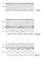
- a massive germanium plate 2(which therefore has good crystalline and electrical properties), here of a typical diameter of 200 mm and a thickness of 750 ⁇ m, on which a layer of surface of silicon oxide 4 (SiO 2 ), for example by PECVD (for " Plasma Enhanced Chemical Vapor Deposition ", ie plasma-enhanced chemical vapor deposition) with a 380 ° SiH 4 chemistry C, as represented in figure 1 .
- germanium plate 2without a surface layer, or one or more surface layers of a different nature.
- the silicon oxide layer 4may optionally be prepared by densification (for example under nitrogen at 600 ° C. for one hour).
- the germanium plate structure 2 - silicon oxide layer 4is then prepared for bonding described hereinafter, for example by chemical cleaning and / or chemical-mechanical polishing for hydrophilic type bonding.
- This structure represented in figure 1is then bonded to a substrate 6 made of a material whose thermal expansion coefficient is different from that of germanium, silicon (Si), which forms a support, on which was optionally formed a layer, for example a layer of silicon oxide (SiO 2 ) 8 formed by thermal oxidation to facilitate the subsequent bonding (oxide / oxide bonding being well controlled).
- a substrate 6made of a material whose thermal expansion coefficient is different from that of germanium, silicon (Si), which forms a support, on which was optionally formed a layer, for example a layer of silicon oxide (SiO 2 ) 8 formed by thermal oxidation to facilitate the subsequent bonding (oxide / oxide bonding being well controlled).
- the assembly of the germanium plate 2 on the silicon substrate 6(with possible interposition of silicon oxide layers 4, 8) is represented during its bonding in figure 2 .
- This bondingcan be consolidated in an oven, for example at 200 ° C for two hours.
- This bondingmay advantageously be carried out hot, for example between 100 ° C. and 200 ° C., which will make it possible to generate in the structure stresses that may compensate for a part of the stresses generated by the subsequent heat treatments and in particular the treatment. thermal fracture, thus reducing the risk of breakage.
- the germanium plate 2is then thinned, preferably by the combination of a grinding followed by a chemical mechanical polishing and possibly a chemical etching (polishing to obtain a good final roughness and the chemical etching of remove the defects created by the rectification).
- a grindingfollowed by a chemical mechanical polishing and possibly a chemical etching (polishing to obtain a good final roughness and the chemical etching of remove the defects created by the rectification).
- Other thinning techniquescould be used, insofar as they guarantee the integrity of the structure (in particular that they do not require excessive temperature rise of the structure).
- the final thickness of germaniummust be such that the mechanical behavior of the germanium / silicon assembly is essentially dictated by the silicon 6, so that this assembly behaves mechanically in temperature as a homo-structure, and more precisely so that the elastic energy stored in the structure during the subsequent heat treatments, and in particular during the heat treatment of fracture (and more particularly at the time of the fracture of the structure), does not lead to breakage of the structure.
- a thickness of 1 ⁇ m to 50 ⁇ m, for example 20 ⁇ m,will be chosen.
- figure 3which thus essentially consists of a substrate 6 forming a support (here in silicon, with a typical thickness of 750 ⁇ m for a substrate of 200 mm in diameter), of an intermediate layer 10 made of silicon oxide (which corresponds to 1 assembly of the two layers of silicon oxide 4, 8 mentioned above) and a thinned germanium layer 3, of reduced thickness, for example of the order of a few micrometers to a few tens of micrometers, for example 20 ⁇ m .
- the roughness and the crystalline structure of the thinned layer of germanium 3are close to those of a solid germanium substrate so that the crystalline and electrical properties of the thin layers formed as described below from the thinned layer of germanium 3 will be particularly good.
- the reduced thickness of the thinned layer of germanium 3 and its bonding on the silicon substrate 6 forming a supportmakes it possible to obtain a structure having a mechanical behavior different from a solid substrate of germanium, which will advantageously be used during the separation step described below.
- this structure(germanium / silicon) allows better heat dissipation during the subsequent technological steps than the solution using a germanium substrate.
- a weakened zone 14is formed in the thinned layer of germanium 3 at a depth which corresponds to the thickness of the thin layer that is to be transferred (generally of the order of a few hundred nanometers, for example between a few tens and 1000 nm), for example by implantation of gaseous species, here hydrogen ions (H + ), with an energy of between a few keV and 250 keV and a dose of between 3.10 16 and 7.10 16 H + / cm 2 ; typically, with an implantation energy of 100 keV and a dose of 5.10 16 , an implantation depth of about 700 nm is obtained.
- gaseous specieshere hydrogen ions (H + )
- the implantation stepis for example performed after the formation of the silicon oxide layer (SiO 2 ) and before cleaning the surface.
- the donor structureis thus constructed as shown in FIG. figure 4 .
- This structureis then bonded (at the level of the silicon oxide layer 12 deposited on the thinned layer of germanium 3, that is to say at the level of the latter surface which has undergone implantation), by for example by a hydrophilic bonding on the support on which the thin layer, mainly consisting of a silicon substrate 18 (generally of thickness of the order of 750 ⁇ m for a substrate of 200 mm thickness) is to be carried forward. covered by a layer of silicon oxide (SiO 2 ) 16.
- the previously mentioned assemblybehaves essentially as a homo-structure and therefore has a good mechanical behavior during the fracture heat treatment step, without major risk of breakage formation.
- the relaxation of the elastic energy stored in the structure at the time of the fractureis controlled and does not lead to breakage of structures obtained after fracture.
- the silicon substrate 18 covered with the silicon oxide layer 24thus carries a thin layer of germanium 22 with good electrical properties because this thin layer 22 is derived from the thinned layer of germanium 3 whose electrical properties are close to those of the initial germanium 2 plate as already mentioned.
- GeOIie germanium on insulator
- the donor structureconsisting mainly of the silicon substrate 6 and the residual layer of germanium 20 (thinned layer of germanium 3 peeled from the thin layer 22), can then be recycled (for example by grinding and / or polishing techniques).
- the donor structureis essentially constituted as it was beforehand, as shown in figure 3 ).
- the thinned layer 3 or the residual germanium layer of the donor structuremay serve as a seed for the germanium epitaxy on this structure. Due to the crystalline quality of the thinned (or residual) layer, the crystalline quality of this epitaxial layer will be close to that of a massive germanium substrate (often referred to as " bulk " germanium). It will be possible to repeat the thin film transfer process using the epitaxial layer.
- the small thickness of the silicon epitaxial layersallows the germanium to impose its mesh parameter and thus maintain a good crystalline quality of the epitaxial layers of germanium.
- the combined thickness of the epitaxial layers and of the initial germanium layer 3remains small enough for the mechanical temperature behavior of the structure obtained to be imposed by the silicon substrate.
- the thin layer of siliconcan be used as a stop layer during successive transfers.
- This methodmakes it possible to avoid polishing after fracture and thus the thickness inhomogeneities that generally result therefrom.
Landscapes
- Engineering & Computer Science (AREA)
- Physics & Mathematics (AREA)
- Condensed Matter Physics & Semiconductors (AREA)
- General Physics & Mathematics (AREA)
- Manufacturing & Machinery (AREA)
- Computer Hardware Design (AREA)
- Microelectronics & Electronic Packaging (AREA)
- Power Engineering (AREA)
- Recrystallisation Techniques (AREA)
- Application Of Or Painting With Fluid Materials (AREA)
Description
Translated fromFrenchL'invention concerne un procédé de report d'une couche mince sur un support. Par couche mince, on entend une couche d'épaisseur typiquement inférieure à 1 µm.The invention relates to a method for transferring a thin layer to a support. Thin layer means a layer of thickness typically less than 1 micron.
Dans le cadre de la réalisation de structures empilées formées notamment par des couches minces portées par un support (par exemple un substrat), il a déjà été proposé de réaliser le report d'une couche mince sur le support selon un procédé qui comprend les étapes principales suivantes :
- la formation d'une zone fragilisée à une profondeur donnée d'un substrat constitué du matériau qui doit former la couche mince, par exemple par implantation d'un gaz à cette profondeur ;
- le collage du substrat implanté (dit substrat donneur) sur le support, par exemple par collage moléculaire ;
- la séparation du substrat donneur amputé de la couche mince (située entre la zone fragilisée et la surface initiale du substrat donneur) et du support qui porte alors la couche mince, par fracture (en général lors d'une étape de traitement thermique, couramment entre 200°C et 600°C) au niveau de la zone précédemment fragilisée.
- forming a weakened zone at a given depth of a substrate consisting of the material which is to form the thin layer, for example by implantation of a gas at this depth;
- bonding the implanted substrate (said donor substrate) to the support, for example by molecular bonding;
- the separation of the amputated donor substrate from the thin layer (situated between the weakened zone and the initial surface of the donor substrate) and the support which then carries the thin layer, by fracture (generally during a heat treatment step, commonly between 200 ° C and 600 ° C) at the previously weakened zone.
Une telle solution est décrite par exemple dans la demande de brevet
Si le procédé brièvement décrit ci-dessus peut être appliqué tel quel dans le cas qui vient d'être mentionné, certaines difficultés peuvent survenir lors de l'application de manière classique de ce procédé dans des contextes différents, par exemple lorsque le substrat donneur et le support ont des caractéristiques mécaniques très différentes.While the method briefly described above can be applied as is in the case just mentioned, certain difficulties may arise when applying this method conventionally in different contexts, for example when the donor substrate and the support have very different mechanical characteristics.
C'est notamment le cas lorsque l'on souhaite remplacer la couche mince de silicium par une couche mince de germanium (Ge) dont certaines propriétés électroniques sont avantageuses (telle que la mobilité des porteurs électriques, ce qui permet une amélioration des performances des circuits réalisés sur germanium).This is particularly the case when it is desired to replace the thin layer of silicon with a thin layer of germanium (Ge), certain electronic properties of which are advantageous (such as the mobility of the electric carriers, which allows an improvement in the performance of the circuits made on germanium).
La réalisation d'une telle structure (dénommée GeOI, pour "Germanium-On-Insulator", c'est-à-dire germanium sur isolant) au moyen du procédé précédemment évoqué a par exemple fait l'objet de l'article "Germanium-On-Insulator (GeOI)Structure Realized by the Smart Cut™ Technology", de F. Letertreet al.,in MRS proceedings, 809 B4.4 (2004).The realization of such a structure (called GeOI, for "Germanium-On-Insulator ", that is to say germanium on insulator) by means of the previously mentioned method has for example been the subject of the article "Germanium -On-Insulator (GeOI)Structure Realized by Smart Cut ™ Technology ", by F. Letertreet al .,In MRS proceedings, 809 B4.4 (2004).
En l'espèce, l'application classique du procédé de report de la couche mince mentionnée précédemment conduit au collage d'un substrat de silicium sur un substrat implanté de germanium, en vue de leur séparation, au niveau de la zone fragilisée par l'implantation, par un traitement thermique. Cette solution est toutefois problématique du fait de la différence importante en termes de coefficient de dilatation thermique des deux matériaux utilisés (2,6.10-6/°C pour le silicium et 58.10-6/°C pour le germanium). En effet, le relâchement brutal, au moment de la fracture, des contraintes emmagasinées dans la structure peut occasionner la casse d'un substrat, voire des deux substrats.In the present case, the conventional application of the method of transfer of the thin layer mentioned above leads to the bonding of a silicon substrate on an implanted substrate of germanium, with a view to their separation, at the level of the zone weakened by the implantation, by a heat treatment. This solution is however problematic because of the significant difference in terms of thermal expansion coefficient of the two materials used (2.6.10-6 / ° C for silicon and 58.10-6 / ° C for germanium). Indeed, the sudden release, at the time of the fracture, the stresses stored in the structure can cause the breakage of a substrate, or both substrates.
Il est également proposé dans l'article précité de réaliser l'implantation dans une couche de germanium, dont l'épaisseur peut varier d'un à quelques microns et formée par épitaxie à la surface d'un substrat de silicium standard (de 750 µm d'épaisseur). Ainsi, la structure soumise au traitement thermique de séparation se comporte comme une homo-structure du fait de la faible épaisseur de germanium devant celle des deux substrats de silicium (voir par exemple
Cette dernière solution est toutefois moins avantageuse sur le plan électronique du fait du nombre important de dislocations et d'une rugosité plus forte dans le germanium épitaxié.This latter solution is however less advantageous electronically because of the large number of dislocations and a higher roughness in the epitaxial germanium.
Une autre solution connue pour réaliser une structure comportant une couche d'un premier matériau sur un substrat d'un second matériau est, après assemblage d'un substrat du premier matériau avec le substrat du second matériau, de procéder à un amincissement mécano-chimique du substrat du premier matériau. Cependant, cette technique ne peut être utilisée pour obtenir des couches minces de l'ordre du micron avec une bonne homogénéité d'épaisseur. En effet, par cette technique, plus l'amincissement est important, plus la couche résiduelle est inhomogène en épaisseur.Another known solution for producing a structure comprising a layer of a first material on a substrate of a second material is, after assembly of a substrate of the first material with the substrate of the second material. second material, to carry out a mechano-chemical thinning of the substrate of the first material. However, this technique can not be used to obtain thin films of the order of one micron with good homogeneity of thickness. Indeed, by this technique, the greater the thinning, the more the residual layer is inhomogeneous in thickness.
Afin de résoudre ces différents problèmes, et de proposer ainsi une solution qui combine notamment une mise en oeuvre simple, une bonne tenue mécanique lors de l'étape de traitement thermique de fracture et de bonnes propriétés cristallines électriques de la structure obtenue, l'invention prévoit un procédé de report d'une couche mince d'un premier matériau en germanium sur un premier support formé d'un second matériau en silicium, comprenant les étapes suivantes :
- fourniture d'une structure comportant une couche dont une partie au moins est issue d'un substrat massif de germanium ou obtenue par croissance épitaxiale en utilisant le substrat massif en Germanium en tant que graine et qui est solidaire d'un second support de silicium, l'épaisseur de la couche étant comprise entre 1 µm et 50 µm ;
- formation dans la couche par implantation d'au moins une espèce gazeuse d'une zone fragilisée enterrée à une profondeur donnée délimitant dans la structure la couche mince à reporter ;
- collage de la couche solidaire du second support sur le premier support ;
- fracture de la couche au niveau de la zone fragilisée incluant au moins une étape de traitement thermique.
- providing a structure comprising a layer at least a portion of which is derived from a solid substrate of germanium or obtained by epitaxial growth using the massive Germanium substrate as a seed and which is integral with a second silicon support, the thickness of the layer being between 1 μm and 50 μm;
- forming in the layer by implantation of at least one gaseous species of a weakened zone buried at a given depth delimiting in the structure the thin layer to be transferred;
- bonding the integral layer of the second support to the first support;
- fracture of the layer at the weakened zone including at least one heat treatment step.
Dans un tel procédé, le second support en silicium permet une bonne coopération mécanique avec le premier support en silicium (évolution similaire en température), indépendamment du matériau de la couche mince à reporter en germanium.In such a method, the second silicon support provides good mechanical cooperation with the first silicon support (similar temperature evolution), regardless of the material of the thin layer to be transferred to germanium.
L'épaisseur de la couche de germanium est de préférence telle que le comportement mécanique en température de la structure obtenue après collage est imposé par le second support en silicum et le premier support en silicium. L'épaisseur de la couche est ainsi suffisamment fine pour ne pas intervenir dans le comportement mécanique en température de la structure obtenue après collage. L'étape de fracture se produit ainsi dans de bonnes conditions.The thickness of the germanium layer is preferably such that the mechanical temperature behavior of the structure obtained after bonding is imposed by the second silicon support and the first silicon support. The thickness of the layer is thus thin enough not to interfere with the mechanical temperature behavior of the structure obtained after bonding. The fracture step thus occurs under good conditions.
Selon l'invention, les épaisseurs mis en jeu, et notamment l'épaisseur de la couche de premier matériau en germanium, sont choisis de sorte que le relâchement des contraintes emmagasinées dans la structure au moment de la fracture n'entraine pas la casse de l'une ou l'autre des structures obtenues après fracture.According to the invention, the thicknesses involved, and in particular the thickness of the layer of first germanium material, are chosen so that the relaxation of the stresses stored in the structure at the time of the fracture does not cause the breakage of one or the other of the structures obtained after fracture.
L'étape de fracture peut également comprendre une étape d'application de sollicitations mécaniques : forces mécaniques (insertion d'une lame, effort de traction et/ou flexion et/ou cisaillement) et/ou ultrasons ou micro-ondes ; l'étape de formation d'une zone fragilisée peut quant à elle être réalisée par implantation d'une ou plusieurs espèces gazeuses.The fracture step can also comprise a step of applying mechanical stresses: mechanical forces (insertion of a blade, tensile force and / or flexion and / or shear) and / or ultrasound or microwaves; the step of forming a weakened zone can in turn be carried out by implantation of one or more gaseous species.
L'épaisseur de la couche solidaire du second support est par exemple inférieure à 15 % de l'épaisseur du second support, ce qui permet d'éviter toute influence mécanique notable de cette couche sur la structure issue de l'étape de collage, et notamment de limiter l'énergie élastique stockée dans la structure lors d'un traitement thermique. Cette épaisseur doit bien sûr être choisie en fonction de la différence des coefficients de dilatation thermique existant au sein de la structure et de la température que devra pouvoir supporter cette structure. Plus cette température sera basse, plus l'épaisseur de la couche solidaire du second support pourra être importante.The thickness of the layer secured to the second support is, for example, less than 15% of the thickness of the second support, which makes it possible to avoid any significant mechanical influence of this layer on the structure resulting from the bonding step, and in particular to limit the elastic energy stored in the structure during a heat treatment. This thickness must of course be chosen according to the difference in thermal expansion coefficients existing within the structure and the temperature that must be able to support this structure. The lower this temperature, the greater the thickness of the layer secured to the second support may be important.
Le second matériau est du silicium. Le premier matériau est quant à lui du germanium.The second material is silicon. The first material is germanium.
L'épaisseur de la couche du premier matériau (avant fracture) est par exemple comprise entre 1 µm et 50 µm.The thickness of the layer of the first material (before fracture) is, for example, between 1 μm and 50 μm.
Selon un mode de réalisation présenté ci-après, le procédé peut comprendre une étape préalable de collage d'une plaque massive du premier matériau sur le second support, par exemple à chaud (typiquement entre 100°C et 200°C). Dans ce cas, la couche issue de la plaque et solidaire du second support peut être obtenue par une étape d'amincissement de la plaque du premier matériau, par exemple par amincissement mécano-chimique (qui peut être réalisé par un procédé dit «grinding », puis par polissage).According to an embodiment presented below, the method may comprise a prior step of bonding a solid plate of the first material to the second support, for example hot (typically between 100 ° C and 200 ° C). In this case, the layer issuing from the plate and integral with the second support can be obtained by a step of thinning the plate of the first material, for example by chemical-mechanical thinning (which can be achieved by a so-called "grinding " process , then by polishing).
Le procédé peut aussi comprendre une étape de dépôt par épitaxie du premier matériau sur une partie de la couche (couche résiduelle) demeurant solidaire du second support après fracture. La qualité cristalline de la couche résiduelle étant bonne, celle de la couche épitaxiée le sera aussi.The method may also comprise a step of epitaxial deposition of the first material on a part of the layer (residual layer) remaining integral with the second support after fracture. The crystalline quality of the residual layer being good, that of the epitaxial layer will be as well.
Ainsi, on peut utiliser la couche épitaxiée pour un nouveau report de couche mince, par exemple au moyen des étapes suivantes :
- formation dans la couche épitaxiée d'une zone fragilisée enterrée ;
- collage de la couche épitaxiée sur un troisième support ;
- fracture de la couche épitaxiée au niveau de la zone fragilisée.
- formation in the epitaxial layer of a buried weakened zone;
- bonding the epitaxial layer to a third support;
- fracture of the epitaxial layer at the weakened zone.
Selon une possibilité de mise en oeuvre du procédé, la couche solidaire du second support est intégralement issue du substrat massif. On assure ainsi une très bonne qualité cristalline pour l'ensemble de la couche.According to one possible implementation of the method, the integral layer of the second support is integrally from the solid substrate. This ensures a very good crystalline quality for the entire layer.
Selon une autre possibilité de mise en oeuvre, la couche solidaire du second support comporte une couche épitaxiée du premier matériau. Comme déjà vu, ceci permet de continuer la réalisation de reports de couches minces sur la base d'une couche résiduelle, tout en conservant une bonne qualité cristalline grâce à la partie issue du substrat massif.According to another possible embodiment, the layer integral with the second support comprises an epitaxial layer of the first material. As already seen, this makes it possible to continue carrying out thin-layer transfers on the basis of a residual layer, while maintaining a good crystalline quality thanks to the part resulting from the solid substrate.
La couche solidaire du second support peut également comporter dans ce cas une couche épitaxiée d'un quatrième matériau d'une épaisseur telle que sa structure cristalline est impartie par le premier matériau. On peut ainsi utiliser cette couche à d'autres fonctions, sans qu'elle ne remette en cause la qualité cristalline des couches du premier matériau.The integral layer of the second support may also comprise in this case an epitaxial layer of a fourth material of a thickness such that its crystalline structure is imparted by the first material. We can thus using this layer to other functions, without it calling into question the crystalline quality of the layers of the first material.
Par exemple, le procédé peut comprendre une étape d'élimination de la couche épitaxiée du premier matériau après fracture utilisant la couche épitaxiée du quatrième matériau comme couche d'arrêt.For example, the method may comprise a step of removing the epitaxial layer of the first material after fracture using the epitaxial layer of the fourth material as a barrier layer.
D'autres caractéristiques et avantages de la présente invention apparaîtront à la lumière de la description qui suit, faite en référence aux dessins annexés dans lesquels les
Sur ces figures, les différentes couches apparaissent avec des épaisseurs schématiques, et non directement proportionnelles à la réalité, afin d'éclaircir leur présentation.In these figures, the different layers appear with schematic thicknesses, and not directly proportional to the reality, in order to clarify their presentation.
Les différentes étapes d'un exemple de procédé selon l'invention vont à présent être décrites en référence à ces figures.The different steps of an exemplary method according to the invention will now be described with reference to these figures.
Dans cet exemple, on utilise une plaque de germanium 2 massif (qui a donc de bonnes propriétés cristallines et électriques), ici d'un diamètre typique de 200 mm et d'une épaisseur de 750 µm, sur laquelle on a déposé une couche de surface d'oxyde de silicium 4 (SiO2), par exemple par PECVD (pour «Plasma Enhanced Chemical Vapor Deposition », c'est-à-dire dépôt chimique en phase vapeur assisté par plasma) avec une chimie SiH4 à 380°C, tel que représenté en
En variante, on pourrait utiliser une plaque de germanium 2 sans couche de surface, ou une ou plusieurs couches de surface d'une nature différente.Alternatively, one could use a
La couche d'oxyde de silicium 4 peut éventuellement être préparée par densification (par exemple sous azote à 600°C pendant une heure). La structure plaque de germanium 2 - couche d'oxyde de silicium 4 est ensuite préparée pour le collage décrit ci-après, par exemple par nettoyage chimique et/ou polissage mécano-chimique pour un collage de type hydrophile.The
Cette structure représentée à la
L'assemblage de la plaque de germanium 2 sur le substrat 6 en silicium (avec interposition éventuelle de couches d'oxyde de silicium 4, 8) est représenté lors de son collage en
Ce collage peut être consolidé en étuve, par exemple à 200°C pendant deux heures.This bonding can be consolidated in an oven, for example at 200 ° C for two hours.
On pourra avantageusement prévoir de réaliser ce collage à chaud, par exemple entre 100°C et 200°C, ce qui permettra de générer dans la structure des contraintes qui pourront venir compenser une partie des contraintes générées par les traitements thermiques ultérieurs et notamment le traitement thermique de fracture, réduisant ainsi les risques de casse.This bonding may advantageously be carried out hot, for example between 100 ° C. and 200 ° C., which will make it possible to generate in the structure stresses that may compensate for a part of the stresses generated by the subsequent heat treatments and in particular the treatment. thermal fracture, thus reducing the risk of breakage.
La plaque de germanium 2 est alors amincie, de préférence par la combinaison d'une rectification suivie d'un polissage mécano-chimique et éventuellement d'une gravure chimique (le polissage permettant d'obtenir une bonne rugosité finale et la gravure chimique d'enlever les défauts créés par la rectification). D'autres techniques d'amincissement pourraient être utilisées, dans la mesure où elles garantissent l'intégrité de la structure (notamment qu'elles ne nécessitent pas de montée en température trop importante de la structure).The
L'épaisseur finale de germanium doit être telle que le comportement mécanique de l'assemblage germanium/silicium soit essentiellement dicté par le silicium 6, de sorte que cet assemblage se comporte mécaniquement en température comme une homo-structure, et plus précisément de sorte que l'énergie élastique emmagasinée dans la structure pendant les traitements thermiques ultérieurs, et notamment lors du traitement thermique de fracture (et plus particulièrement au moment de la fracture de la structure), ne conduise pas à la casse de la structure. On choisira typiquement pour cette couche de germanium une épaisseur de 1 µm à 50 µm, par exemple de 20 µm.The final thickness of germanium must be such that the mechanical behavior of the germanium / silicon assembly is essentially dictated by the
On obtient alors la structure représentée à la
Du fait du procédé utilisé pour son obtention, la rugosité et la structure cristalline de la couche amincie de germanium 3 sont proches de celles d'un substrat massif de germanium de sorte que les propriétés cristallines et électriques des couches minces formées comme décrit ci-après à partir de la couche amincie de germanium 3 seront particulièrement bonnes.Due to the process used to obtain it, the roughness and the crystalline structure of the thinned layer of
Comme expliqué dans la suite, l'épaisseur réduite de la couche amincie de germanium 3 et son collage sur le substrat de silicium 6 formant support permettent toutefois d'obtenir une structure ayant un comportement mécanique différent d'un substrat massif de germanium, ce qui sera avantageusement utilisé lors de l'étape de séparation décrite plus bas.As explained below, the reduced thickness of the thinned layer of
De plus, du fait de la plus grande conductivité thermique du silicium par rapport au germanium, cette structure (germanium/silicium) permet une meilleure évacuation de la chaleur pendant les étapes technologiques ultérieures que la solution utilisant un substrat de germanium.In addition, because of the greater thermal conductivity of silicon with respect to germanium, this structure (germanium / silicon) allows better heat dissipation during the subsequent technological steps than the solution using a germanium substrate.
La structure qui vient d'être décrite et représentée à la
Avant collage sur le support qui doit recevoir la couche mince (pour l'essentiel un substrat de silicium dans l'exemple décrit ici), on peut préparer la structure précédemment réalisée et représentée à la
- dépôt d'une couche de dioxyde de silicium (SiO2), par exemple comme précédemment par PECVD ;
- densification facultative de la couche d'oxyde de silicium sous azote entre 400°C et 600°C pendant une heure ;
- nettoyage et/ou polissage mécano-chimique (pour améliorer la compatibilité avec un collage hydrophile).
- deposition of a layer of silicon dioxide (SiO2 ), for example as previously by PECVD;
- optional densification of the silicon oxide layer under nitrogen between 400 ° C and 600 ° C for one hour;
- cleaning and / or chemical mechanical polishing (to improve compatibility with hydrophilic bonding).
En variante, il est bien sûr possible de ne pas déposer d'oxyde et de préparer directement la surface de germanium en vue de son collage sur le support devant recevoir la couche mince.Alternatively, it is of course possible not to deposit oxide and prepare the germanium surface directly for its bonding on the support to receive the thin layer.
On forme par ailleurs une zone fragilisée 14 dans la couche amincie de germanium 3, à une profondeur qui correspond à l'épaisseur de la couche mince que l'on souhaite reporter (en général de l'ordre de quelques centaines de nanomètres, par exemple entre quelques dizaines et 1000 nm), par exemple par implantation d'espèces gazeuses, ici des ions hydrogènes (H+), avec une énergie comprise entre quelques keV et 250 keV et une dose comprise entre 3.1016 et 7.1016 H+/cm2 ; typiquement, avec une énergie d'implantation de 100 keV et une dose de 5.1016, on obtient une profondeur d'implantation d'environ 700 nm.Furthermore, a weakened
L'étape d'implantation est par exemple réalisée après la formation de la couche d'oxyde de silicium (SiO2) et avant nettoyage de la surface.The implantation step is for example performed after the formation of the silicon oxide layer (SiO2 ) and before cleaning the surface.
Après cette étape d'implantation et ces étapes éventuelles de préparation, la structure donneuse est donc construite comme représenté à la
Cette structure est alors collée (au niveau de la couche d'oxyde de silicium 12 déposée sur la couche amincie de germanium 3, c'est-à-dire au niveau de la surface de cette dernière qui a subi l'implantation), par exemple par un collage hydrophile sur le support sur lequel doit être reportée la couche mince, constitué ici principalement d'un substrat en silicium 18 (en général d'épaisseur de l'ordre de 750 µm pour un substrat de 200 mm d'épaisseur), recouvert par une couche d'oxyde de silicium (SiO2) 16.This structure is then bonded (at the level of the
On obtient ainsi l'assemblage représenté à la
On réalise ainsi la séparation du support formé par le substrat en silicium 18 recouvert par la couche d'oxyde de silicium 16, qui porte désormais une couche mince de germanium 22 (issue de la couche amincie 3), et de la structure donneuse pelée de cette couche mince transférée, comme représenté à la
Du fait de la faible épaisseur de la couche amincie de germanium 3 par rapport aux substrats en silicium 6, 18 (schématiquement représentée sur les figures, en pratique dans un rapport de l'ordre d'au moins 1 à 10) et de la compatibilité mécanique (ici en termes de dilatation thermique) des deux substrats 6, 18 (ici réalisés dans le même matériau), l'assemblage précédemment mentionné (et représenté à la
Le relâchement de l'énergie élastique emmagasinée dans la structure au moment de la fracture est contrôlé et ne conduit pas à la casse des structures obtenues après fracture.The relaxation of the elastic energy stored in the structure at the time of the fracture is controlled and does not lead to breakage of structures obtained after fracture.
Après l'étape de fracture de la zone fragilisée (et par conséquent de séparation de l'assemblage de la
On obtient ainsi, après d'éventuels traitements de finition du type polissage et recuit thermique, une plaque de GeOI (i.e. de germanium sur isolant) avec des propriétés électriques de la couche de germanium particulièrement intéressantes.Thus, after possible finishing treatments of the polishing and thermal annealing type, a GeOI (ie germanium on insulator) plate with particularly interesting electrical properties of the germanium layer is obtained.
La structure donneuse, constituée principalement du substrat de silicium 6 et de la couche résiduelle de germanium 20 (couche amincie de germanium 3 pelée de la couche mince 22), peut alors être recyclée (par exemple par des techniques de rectification et/ou polissage) afin d'être à nouveau utilisée comme une structure donneuse pour le report d'une nouvelle couche mince de germanium, dans ce cas issue de la couche résiduelle 20 (en effet, même pelée de la couche mince 22, la structure donneuse est essentiellement constituée comme elle l'était au préalable, comme représenté à la
Selon une possibilité de réalisation avantageuse, la couche amincie 3 ou la couche résiduelle 20 de germanium de la structure donneuse peut servir de germe pour l'épitaxie de germanium sur cette structure. Du fait de la qualité cristalline de la couche amincie (ou résiduelle), la qualité cristalline de cette couche épitaxiée sera proche de celle d'un substrat massif de germanium (souvent dénommé germanium «bulk »). On pourra ainsi réitérer le processus de report de couche mince en utilisant la couche épitaxiée.According to an advantageous embodiment, the thinned
En variante, on peut également prévoir d'épitaxier (sur la couche amincie 3 ou la couche résiduelle 20) successivement et itérativement du germanium (sur une épaisseur de quelques microns, par exemple 2 µm) et du silicium (typiquement avec une épaisseur de quelques nanomètres) pour former un empilement alternatif de ces deux matériaux : Si/Ge/Si/Ge etc.Alternatively, one can also provide epitaxial (on the thinned
La faible épaisseur des couches épitaxiées de silicium permet au germanium d'imposer son paramètre de maille et ainsi de maintenir une bonne qualité cristalline des couches épitaxiées de germanium.The small thickness of the silicon epitaxial layers allows the germanium to impose its mesh parameter and thus maintain a good crystalline quality of the epitaxial layers of germanium.
Il faut en revanche s'assurer que l'épaisseur combinée des couches épitaxiées et de la couche de germanium initiale 3, 20 reste suffisamment faible pour que le comportement mécanique en température de la structure obtenue soit imposé par le substrat de silicium.On the other hand, it must be ensured that the combined thickness of the epitaxial layers and of the
Selon cette variante, on peut se servir de la couche mince de silicium comme couche d'arrêt lors des transferts successifs.According to this variant, the thin layer of silicon can be used as a stop layer during successive transfers.
On peut aussi utiliser le procédé suivant :
- on réalise l'implantation dans la couche epitaxiée de germanium située au sommet de l'empilement (couche extérieure) pour définir dans cette couche la couche mince à reporter ;
- on réalise le report de la couche mince comme indiqué ci-dessus ;
- on élimine le reste de la couche extérieure de germanium par gravure sélective (par exemple H2O2) ;
- on élimine ensuite la couche d'arrêt de silicium par gravure sélective (par exemple à base de TMAH - hydroxyde de tetramethylammonium) ;
- on réitère le processus sur la couche de germanium suivante.
- implantation is carried out in the epitaxial layer of germanium located at the top of the stack (outer layer) to define in this layer the thin layer to be transferred;
- the transfer of the thin layer is carried out as indicated above;
- the remainder of the outer layer of germanium is removed by selective etching (for example H2 O2 );
- the silicon stopper is then removed by selective etching (for example based on TMAH-tetramethylammonium hydroxide);
- the process is repeated on the next germanium layer.
Ce procédé permet d'éviter la mise en oeuvre d'un polissage après fracture et ainsi les inhomogénéités d'épaisseur qui en découlent généralement.This method makes it possible to avoid polishing after fracture and thus the thickness inhomogeneities that generally result therefrom.
Claims (11)
- Method for transferring a thin layer (22) of germanium onto a first silicon support (18, 24), comprising the following steps:- providing a structure including a layer (3) at least one part of which is obtained from a bulk germanium substrate or obtained by epitaxial growth using the bulk germanium substrate as a seed and that is attached to a second silicon support (6, 10), the thickness of the layer being between 1 µm and 50 µm;- forming in the layer (3), by implanting at least one gaseous species, a weakened zone (14) buried to a given depth delimiting in the structure the thin layer (22) to be transferred;- bonding the layer (3) attached to the second support (6, 10) to the first support (18, 24);- fracturing the layer (3) in the weakened zone (14), including at least one heat treatment step.
- Thin layer transfer method according to Claim 1, wherein the fracture step also includes a step of applying mechanical loads.
- Thin layer transfer method according to Claim 1 or 2, including a preliminary step of bonding a bulk plate (2) of germanium to the second support (6, 8).
- Thin layer transfer method according to Claim 3, wherein the bonding step is carried out at a temperature between 100°C and 200°C.
- Thin layer transfer method according to Claim 3 or 4, including a step of thinning said plate (2) in order to obtain the layer (3) attached to the second support (6, 10).
- Thin layer transfer method according to one of Claims 1 to 5, including a step of epitaxial deposition of germanium on a portion (20) of the layer (3) remaining attached to the second support (6) after fracture.
- Thin layer transfer method according to Claim 6, including the following steps:- forming a buried weakened zone in the epitaxial layer;- bonding the epitaxial layer onto a third support;- fracturing the epitaxial layer at the weakened zone.
- Thin layer transfer method according to one of Claims 1 to 7, wherein the layer attached to the second support is obtained entirely from the bulk substrate.
- Thin layer transfer method according to one of Claims 1 to 7, wherein the layer attached to the second support includes an epitaxial germanium layer.
- Thin layer transfer method according to Claim 9, wherein the layer attached to the second support includes an epitaxial layer of a material having a thickness such that its crystalline structure is imparted by the germanium.
- Thin layer transfer method according to Claim 10, including a step of eliminating the epitaxial germanium layer after fracture using the epitaxial layer of said material as a stop layer.
Applications Claiming Priority (2)
| Application Number | Priority Date | Filing Date | Title |
|---|---|---|---|
| FR0508555AFR2889887B1 (en) | 2005-08-16 | 2005-08-16 | METHOD FOR DEFERING A THIN LAYER ON A SUPPORT |
| PCT/FR2006/001945WO2007020351A1 (en) | 2005-08-16 | 2006-08-11 | Method of transferring a thin film onto a support |
Publications (2)
| Publication Number | Publication Date |
|---|---|
| EP1922752A1 EP1922752A1 (en) | 2008-05-21 |
| EP1922752B1true EP1922752B1 (en) | 2015-11-04 |
Family
ID=36591309
Family Applications (1)
| Application Number | Title | Priority Date | Filing Date |
|---|---|---|---|
| EP06794326.6ANot-in-forceEP1922752B1 (en) | 2005-08-16 | 2006-08-11 | Method of transferring a thin film onto a support |
Country Status (5)
| Country | Link |
|---|---|
| US (1) | US8142593B2 (en) |
| EP (1) | EP1922752B1 (en) |
| JP (1) | JP5258564B2 (en) |
| FR (1) | FR2889887B1 (en) |
| WO (1) | WO2007020351A1 (en) |
Families Citing this family (20)
| Publication number | Priority date | Publication date | Assignee | Title |
|---|---|---|---|---|
| FR2748851B1 (en) | 1996-05-15 | 1998-08-07 | Commissariat Energie Atomique | PROCESS FOR PRODUCING A THIN FILM OF SEMICONDUCTOR MATERIAL |
| FR2773261B1 (en)* | 1997-12-30 | 2000-01-28 | Commissariat Energie Atomique | METHOD FOR THE TRANSFER OF A THIN FILM COMPRISING A STEP OF CREATING INCLUSIONS |
| FR2848336B1 (en) | 2002-12-09 | 2005-10-28 | Commissariat Energie Atomique | METHOD FOR PRODUCING A STRESS STRUCTURE FOR DISSOCIATING |
| FR2856844B1 (en) | 2003-06-24 | 2006-02-17 | Commissariat Energie Atomique | HIGH PERFORMANCE CHIP INTEGRATED CIRCUIT |
| FR2861497B1 (en)* | 2003-10-28 | 2006-02-10 | Soitec Silicon On Insulator | METHOD FOR CATASTROPHIC TRANSFER OF A FINE LAYER AFTER CO-IMPLANTATION |
| FR2891281B1 (en) | 2005-09-28 | 2007-12-28 | Commissariat Energie Atomique | METHOD FOR MANUFACTURING A THIN FILM ELEMENT |
| FR2910179B1 (en) | 2006-12-19 | 2009-03-13 | Commissariat Energie Atomique | METHOD FOR MANUFACTURING THIN LAYERS OF GaN BY IMPLANTATION AND RECYCLING OF A STARTING SUBSTRATE |
| JP4290745B2 (en)* | 2007-03-16 | 2009-07-08 | 豊田合成株式会社 | Method for manufacturing group III-V semiconductor device |
| FR2947098A1 (en) | 2009-06-18 | 2010-12-24 | Commissariat Energie Atomique | METHOD OF TRANSFERRING A THIN LAYER TO A TARGET SUBSTRATE HAVING A THERMAL EXPANSION COEFFICIENT DIFFERENT FROM THAT OF THE THIN LAYER |
| DE102009053262A1 (en)* | 2009-11-13 | 2011-05-19 | Institut Für Solarenergieforschung Gmbh | A method for forming thin semiconductor layer substrates and method for producing a semiconductor device, in particular a solar cell, with such a semiconductor layer substrate |
| US8367519B2 (en)* | 2009-12-30 | 2013-02-05 | Memc Electronic Materials, Inc. | Method for the preparation of a multi-layered crystalline structure |
| US9257339B2 (en)* | 2012-05-04 | 2016-02-09 | Silicon Genesis Corporation | Techniques for forming optoelectronic devices |
| US8735219B2 (en) | 2012-08-30 | 2014-05-27 | Ziptronix, Inc. | Heterogeneous annealing method and device |
| EP2912685B1 (en)* | 2012-10-26 | 2020-04-08 | RFHIC Corporation | Semiconductor devices with improved reliability and operating life and methods of manufacturing the same |
| US9356188B2 (en) | 2013-09-06 | 2016-05-31 | Veeco Instruments, Inc. | Tensile separation of a semiconducting stack |
| KR102180089B1 (en) | 2013-12-30 | 2020-11-18 | 삼성디스플레이 주식회사 | Method of manufacturing flexible substrate and method of manufacturing display device using the same |
| KR101889352B1 (en) | 2016-09-13 | 2018-08-20 | 한국과학기술연구원 | Semicondutor device including strained germanium and method for manufacturing the same |
| FR3074608B1 (en)* | 2017-12-05 | 2019-12-06 | Soitec | PROCESS FOR THE PREPARATION OF A RESIDUE OF A DONOR SUBSTRATE, SUBSTRATE OBTAINED AT THE END OF THIS PROCESS, AND USE OF SUCH A SUBSTRATE |
| FR3079346B1 (en)* | 2018-03-26 | 2020-05-29 | Soitec | METHOD FOR MANUFACTURING A DONOR SUBSTRATE FOR TRANSFERRING A PIEZOELECTRIC LAYER, AND METHOD FOR TRANSFERRING SUCH A PIEZOELECTRIC LAYER |
| JP7314257B2 (en) | 2018-09-19 | 2023-07-25 | アカーシュ・システムズ・インコーポレイテッド | System and method for satellite communications |
Family Cites Families (250)
| Publication number | Priority date | Publication date | Assignee | Title |
|---|---|---|---|---|
| US3915757A (en) | 1972-08-09 | 1975-10-28 | Niels N Engel | Ion plating method and product therefrom |
| US3913520A (en) | 1972-08-14 | 1975-10-21 | Precision Thin Film Corp | High vacuum deposition apparatus |
| US3993909A (en) | 1973-03-16 | 1976-11-23 | U.S. Philips Corporation | Substrate holder for etching thin films |
| FR2245779B1 (en)* | 1973-09-28 | 1978-02-10 | Cit Alcatel | |
| US3901423A (en) | 1973-11-26 | 1975-08-26 | Purdue Research Foundation | Method for fracturing crystalline materials |
| US4170662A (en) | 1974-11-05 | 1979-10-09 | Eastman Kodak Company | Plasma plating |
| US4121334A (en) | 1974-12-17 | 1978-10-24 | P. R. Mallory & Co. Inc. | Application of field-assisted bonding to the mass production of silicon type pressure transducers |
| US3957107A (en)* | 1975-02-27 | 1976-05-18 | The United States Of America As Represented By The Secretary Of The Air Force | Thermal switch |
| US4039416A (en) | 1975-04-21 | 1977-08-02 | White Gerald W | Gasless ion plating |
| GB1542299A (en)* | 1976-03-23 | 1979-03-14 | Warner Lambert Co | Blade shields |
| US4028149A (en)* | 1976-06-30 | 1977-06-07 | Ibm Corporation | Process for forming monocrystalline silicon carbide on silicon substrates |
| US4074139A (en)* | 1976-12-27 | 1978-02-14 | Rca Corporation | Apparatus and method for maskless ion implantation |
| US4108751A (en) | 1977-06-06 | 1978-08-22 | King William J | Ion beam implantation-sputtering |
| US4179324A (en) | 1977-11-28 | 1979-12-18 | Spire Corporation | Process for fabricating thin film and glass sheet laminate |
| DE2849184A1 (en)* | 1978-11-13 | 1980-05-22 | Bbc Brown Boveri & Cie | METHOD FOR PRODUCING A DISC-SHAPED SILICON SEMICONDUCTOR COMPONENT WITH NEGATIVE BEVELING |
| JPS55104057A (en)* | 1979-02-02 | 1980-08-09 | Hitachi Ltd | Ion implantation device |
| US4324631A (en)* | 1979-07-23 | 1982-04-13 | Spin Physics, Inc. | Magnetron sputtering of magnetic materials |
| CH640886A5 (en) | 1979-08-02 | 1984-01-31 | Balzers Hochvakuum | METHOD FOR APPLYING HARD WEAR-RESISTANT COATS ON DOCKS. |
| US4244348A (en)* | 1979-09-10 | 1981-01-13 | Atlantic Richfield Company | Process for cleaving crystalline materials |
| FR2506344B2 (en)* | 1980-02-01 | 1986-07-11 | Commissariat Energie Atomique | SEMICONDUCTOR DOPING PROCESS |
| FR2475068B1 (en)* | 1980-02-01 | 1986-05-16 | Commissariat Energie Atomique | SEMICONDUCTOR DOPING PROCESS |
| US4471003A (en) | 1980-11-25 | 1984-09-11 | Cann Gordon L | Magnetoplasmadynamic apparatus and process for the separation and deposition of materials |
| FR2501727A1 (en) | 1981-03-13 | 1982-09-17 | Vide Traitement | PROCESS FOR THE THERMOCHEMICAL TREATMENT OF METALS BY ION BOMBING |
| US4361600A (en) | 1981-11-12 | 1982-11-30 | General Electric Company | Method of making integrated circuits |
| US4412868A (en) | 1981-12-23 | 1983-11-01 | General Electric Company | Method of making integrated circuits utilizing ion implantation and selective epitaxial growth |
| US4486247A (en) | 1982-06-21 | 1984-12-04 | Westinghouse Electric Corp. | Wear resistant steel articles with carbon, oxygen and nitrogen implanted in the surface thereof |
| FR2529383A1 (en)* | 1982-06-24 | 1983-12-30 | Commissariat Energie Atomique | MECHANICAL SCANNING TARGET HOLDER USABLE IN PARTICULAR FOR THE IMPLANTATION OF IORIS |
| FR2537768A1 (en) | 1982-12-08 | 1984-06-15 | Commissariat Energie Atomique | METHOD AND DEVICE FOR OBTAINING SPATIALLY MODULATED DENSITY PARTICLE BEAMS, APPLICATION TO ION ETCHING AND IMPLANTATION |
| FR2537777A1 (en)* | 1982-12-10 | 1984-06-15 | Commissariat Energie Atomique | METHOD AND DEVICE FOR IMPLANTATION OF PARTICLES IN A SOLID |
| DE3246480A1 (en) | 1982-12-15 | 1984-06-20 | Wacker-Chemitronic Gesellschaft für Elektronik-Grundstoffe mbH, 8263 Burghausen | METHOD FOR THE PRODUCTION OF SEMICONDUCTOR DISC WITH CUTTING DISC REAR SIDE |
| US4500563A (en)* | 1982-12-15 | 1985-02-19 | Pacific Western Systems, Inc. | Independently variably controlled pulsed R.F. plasma chemical vapor processing |
| US4468309A (en) | 1983-04-22 | 1984-08-28 | White Engineering Corporation | Method for resisting galling |
| GB2144343A (en)* | 1983-08-02 | 1985-03-06 | Standard Telephones Cables Ltd | Optical fibre manufacture |
| US4567505A (en)* | 1983-10-27 | 1986-01-28 | The Board Of Trustees Of The Leland Stanford Junior University | Heat sink and method of attaching heat sink to a semiconductor integrated circuit and the like |
| JPS6088535U (en) | 1983-11-24 | 1985-06-18 | 住友電気工業株式会社 | semiconductor wafer |
| FR2558263B1 (en) | 1984-01-12 | 1986-04-25 | Commissariat Energie Atomique | DIRECTIVE ACCELEROMETER AND METHOD FOR MANUFACTURING IT WITH MICROLITHOGRAPHY |
| GB2155024A (en) | 1984-03-03 | 1985-09-18 | Standard Telephones Cables Ltd | Surface treatment of plastics materials |
| FR2563377B1 (en) | 1984-04-19 | 1987-01-23 | Commissariat Energie Atomique | METHOD FOR MANUFACTURING AN INSULATING LAYER BURIED IN A SEMICONDUCTOR SUBSTRATE, BY ION IMPLANTATION |
| US4542863A (en) | 1984-07-23 | 1985-09-24 | Larson Edwin L | Pipe-thread sealing tape reel with tape retarding element |
| US4566403A (en)* | 1985-01-30 | 1986-01-28 | Sovonics Solar Systems | Apparatus for microwave glow discharge deposition |
| US4837172A (en)* | 1986-07-18 | 1989-06-06 | Matsushita Electric Industrial Co., Ltd. | Method for removing impurities existing in semiconductor substrate |
| US4717683A (en)* | 1986-09-23 | 1988-01-05 | Motorola Inc. | CMOS process |
| US4764394A (en) | 1987-01-20 | 1988-08-16 | Wisconsin Alumni Research Foundation | Method and apparatus for plasma source ion implantation |
| JPS63254762A (en)* | 1987-04-13 | 1988-10-21 | Nissan Motor Co Ltd | CMOS semiconductor device |
| US4847792A (en) | 1987-05-04 | 1989-07-11 | Texas Instruments Incorporated | Process and apparatus for detecting aberrations in production process operations |
| SE458398B (en) | 1987-05-27 | 1989-03-20 | H Biverot | LIGHT DETECTING AND LIGHTING DETERMINATION DEVICE |
| FR2616590B1 (en) | 1987-06-15 | 1990-03-02 | Commissariat Energie Atomique | METHOD FOR MANUFACTURING AN INSULATOR LAYER BURIED IN A SEMICONDUCTOR SUBSTRATE BY ION IMPLANTATION AND SEMICONDUCTOR STRUCTURE COMPRISING THIS LAYER |
| US4956698A (en) | 1987-07-29 | 1990-09-11 | The United States Of America As Represented By The Department Of Commerce | Group III-V compound semiconductor device having p-region formed by Be and Group V ions |
| US4846928A (en) | 1987-08-04 | 1989-07-11 | Texas Instruments, Incorporated | Process and apparatus for detecting aberrations in production process operations |
| US4887005A (en) | 1987-09-15 | 1989-12-12 | Rough J Kirkwood H | Multiple electrode plasma reactor power distribution system |
| US5015353A (en)* | 1987-09-30 | 1991-05-14 | The United States Of America As Represented By The Secretary Of The Navy | Method for producing substoichiometric silicon nitride of preselected proportions |
| US5138422A (en) | 1987-10-27 | 1992-08-11 | Nippondenso Co., Ltd. | Semiconductor device which includes multiple isolated semiconductor segments on one chip |
| GB8725497D0 (en) | 1987-10-30 | 1987-12-02 | Atomic Energy Authority Uk | Isolation of silicon |
| US5200805A (en)* | 1987-12-28 | 1993-04-06 | Hughes Aircraft Company | Silicon carbide:metal carbide alloy semiconductor and method of making the same |
| US4904610A (en)* | 1988-01-27 | 1990-02-27 | General Instrument Corporation | Wafer level process for fabricating passivated semiconductor devices |
| DE3803424C2 (en)* | 1988-02-05 | 1995-05-18 | Gsf Forschungszentrum Umwelt | Method for the quantitative, depth-differential analysis of solid samples |
| JP2666945B2 (en)* | 1988-02-08 | 1997-10-22 | 株式会社東芝 | Method for manufacturing semiconductor device |
| US4894709A (en)* | 1988-03-09 | 1990-01-16 | Massachusetts Institute Of Technology | Forced-convection, liquid-cooled, microchannel heat sinks |
| US4853250A (en) | 1988-05-11 | 1989-08-01 | Universite De Sherbrooke | Process of depositing particulate material on a substrate |
| NL8802028A (en) | 1988-08-16 | 1990-03-16 | Philips Nv | METHOD FOR MANUFACTURING AN APPARATUS |
| JP2670623B2 (en) | 1988-09-19 | 1997-10-29 | アネルバ株式会社 | Microwave plasma processing equipment |
| US4952273A (en) | 1988-09-21 | 1990-08-28 | Microscience, Inc. | Plasma generation in electron cyclotron resonance |
| US4996077A (en)* | 1988-10-07 | 1991-02-26 | Texas Instruments Incorporated | Distributed ECR remote plasma processing and apparatus |
| US4891329A (en)* | 1988-11-29 | 1990-01-02 | University Of North Carolina | Method of forming a nonsilicon semiconductor on insulator structure |
| NL8900388A (en) | 1989-02-17 | 1990-09-17 | Philips Nv | METHOD FOR JOINING TWO OBJECTS |
| JPH02302044A (en)* | 1989-05-16 | 1990-12-14 | Fujitsu Ltd | Manufacturing method of semiconductor device |
| US4929566A (en)* | 1989-07-06 | 1990-05-29 | Harris Corporation | Method of making dielectrically isolated integrated circuits using oxygen implantation and expitaxial growth |
| JPH0355822A (en) | 1989-07-25 | 1991-03-11 | Shin Etsu Handotai Co Ltd | Manufacture of substrate for forming semiconductor element |
| US4948458A (en) | 1989-08-14 | 1990-08-14 | Lam Research Corporation | Method and apparatus for producing magnetically-coupled planar plasma |
| US5036023A (en) | 1989-08-16 | 1991-07-30 | At&T Bell Laboratories | Rapid thermal processing method of making a semiconductor device |
| US5013681A (en)* | 1989-09-29 | 1991-05-07 | The United States Of America As Represented By The Secretary Of The Navy | Method of producing a thin silicon-on-insulator layer |
| US5310446A (en)* | 1990-01-10 | 1994-05-10 | Ricoh Company, Ltd. | Method for producing semiconductor film |
| JPH0650738B2 (en) | 1990-01-11 | 1994-06-29 | 株式会社東芝 | Semiconductor device and manufacturing method thereof |
| US5034343A (en) | 1990-03-08 | 1991-07-23 | Harris Corporation | Manufacturing ultra-thin wafer using a handle wafer |
| CN1018844B (en) | 1990-06-02 | 1992-10-28 | 中国科学院兰州化学物理研究所 | Antirust dry film lubricant |
| JPH0719739B2 (en) | 1990-09-10 | 1995-03-06 | 信越半導体株式会社 | Bonded wafer manufacturing method |
| US5198371A (en)* | 1990-09-24 | 1993-03-30 | Biota Corp. | Method of making silicon material with enhanced surface mobility by hydrogen ion implantation |
| US5618739A (en)* | 1990-11-15 | 1997-04-08 | Seiko Instruments Inc. | Method of making light valve device using semiconductive composite substrate |
| US5300788A (en)* | 1991-01-18 | 1994-04-05 | Kopin Corporation | Light emitting diode bars and arrays and method of making same |
| DE4106288C2 (en) | 1991-02-28 | 2001-05-31 | Bosch Gmbh Robert | Sensor for measuring pressures or accelerations |
| JP2812405B2 (en) | 1991-03-15 | 1998-10-22 | 信越半導体株式会社 | Semiconductor substrate manufacturing method |
| US5110748A (en)* | 1991-03-28 | 1992-05-05 | Honeywell Inc. | Method for fabricating high mobility thin film transistors as integrated drivers for active matrix display |
| US5442205A (en) | 1991-04-24 | 1995-08-15 | At&T Corp. | Semiconductor heterostructure devices with strained semiconductor layers |
| US5256581A (en) | 1991-08-28 | 1993-10-26 | Motorola, Inc. | Silicon film with improved thickness control |
| FR2681472B1 (en) | 1991-09-18 | 1993-10-29 | Commissariat Energie Atomique | PROCESS FOR PRODUCING THIN FILMS OF SEMICONDUCTOR MATERIAL. |
| JP3416163B2 (en)* | 1992-01-31 | 2003-06-16 | キヤノン株式会社 | Semiconductor substrate and manufacturing method thereof |
| JPH05235312A (en)* | 1992-02-19 | 1993-09-10 | Fujitsu Ltd | Semiconductor substrate and its manufacture |
| US5614019A (en)* | 1992-06-08 | 1997-03-25 | Air Products And Chemicals, Inc. | Method for the growth of industrial crystals |
| US5234535A (en) | 1992-12-10 | 1993-08-10 | International Business Machines Corporation | Method of producing a thin silicon-on-insulator layer |
| WO1994017558A1 (en) | 1993-01-29 | 1994-08-04 | The Regents Of The University Of California | Monolithic passive component |
| US5400458A (en)* | 1993-03-31 | 1995-03-28 | Minnesota Mining And Manufacturing Company | Brush segment for industrial brushes |
| FR2714524B1 (en)* | 1993-12-23 | 1996-01-26 | Commissariat Energie Atomique | PROCESS FOR MAKING A RELIEF STRUCTURE ON A SUPPORT IN SEMICONDUCTOR MATERIAL |
| DE69423594T2 (en)* | 1993-12-28 | 2000-07-20 | Honda Giken Kogyo K.K., Tokio/Tokyo | Gas supply mechanism for gas internal combustion engine |
| DE4400985C1 (en)* | 1994-01-14 | 1995-05-11 | Siemens Ag | Method for producing a three-dimensional circuit arrangement |
| FR2715501B1 (en) | 1994-01-26 | 1996-04-05 | Commissariat Energie Atomique | Method for depositing semiconductor wafers on a support. |
| FR2715502B1 (en) | 1994-01-26 | 1996-04-05 | Commissariat Energie Atomique | Structure having cavities and method for producing such a structure. |
| FR2715503B1 (en) | 1994-01-26 | 1996-04-05 | Commissariat Energie Atomique | Substrate for integrated components comprising a thin layer and its production method. |
| JP3293736B2 (en) | 1996-02-28 | 2002-06-17 | キヤノン株式会社 | Semiconductor substrate manufacturing method and bonded substrate |
| JP3352340B2 (en) | 1995-10-06 | 2002-12-03 | キヤノン株式会社 | Semiconductor substrate and method of manufacturing the same |
| US5880010A (en)* | 1994-07-12 | 1999-03-09 | Sun Microsystems, Inc. | Ultrathin electronics |
| JPH0851103A (en) | 1994-08-08 | 1996-02-20 | Fuji Electric Co Ltd | Thin film generation method |
| US5524339A (en)* | 1994-09-19 | 1996-06-11 | Martin Marietta Corporation | Method for protecting gallium arsenide mmic air bridge structures |
| FR2725074B1 (en)* | 1994-09-22 | 1996-12-20 | Commissariat Energie Atomique | METHOD FOR MANUFACTURING A STRUCTURE COMPRISING A THIN SEMI-CONDUCTIVE LAYER ON A SUBSTRATE |
| US5567654A (en) | 1994-09-28 | 1996-10-22 | International Business Machines Corporation | Method and workpiece for connecting a thin layer to a monolithic electronic module's surface and associated module packaging |
| DE69502709T2 (en)* | 1994-10-18 | 1998-12-24 | Philips Electronics N.V., Eindhoven | METHOD AND PRODUCTION OF A THIN SILICON OXIDE LAYER |
| EP0799495A4 (en)* | 1994-11-10 | 1999-11-03 | Lawrence Semiconductor Researc | SILICON-GERMANIUM-CARBON COMPOSITIONS AND RELATED PROCESSES |
| ATE216802T1 (en) | 1994-12-12 | 2002-05-15 | Advanced Micro Devices Inc | METHOD FOR PRODUCING BURNED OXIDE LAYERS |
| JP3381443B2 (en) | 1995-02-02 | 2003-02-24 | ソニー株式会社 | Method for separating semiconductor layer from substrate, method for manufacturing semiconductor device, and method for manufacturing SOI substrate |
| FR2736934B1 (en) | 1995-07-21 | 1997-08-22 | Commissariat Energie Atomique | METHOD FOR MANUFACTURING A STRUCTURE WITH A USEFUL LAYER MAINTAINED A DISTANCE FROM A SUBSTRATE BY STOPS, AND FOR DISCONNECTING SUCH A LAYER |
| FR2738671B1 (en)* | 1995-09-13 | 1997-10-10 | Commissariat Energie Atomique | PROCESS FOR PRODUCING THIN FILMS WITH SEMICONDUCTOR MATERIAL |
| FR2744285B1 (en) | 1996-01-25 | 1998-03-06 | Commissariat Energie Atomique | METHOD FOR TRANSFERRING A THIN FILM FROM AN INITIAL SUBSTRATE TO A FINAL SUBSTRATE |
| FR2747506B1 (en) | 1996-04-11 | 1998-05-15 | Commissariat Energie Atomique | PROCESS FOR OBTAINING A THIN FILM OF SEMICONDUCTOR MATERIAL INCLUDING IN PARTICULAR ELECTRONIC COMPONENTS |
| FR2748850B1 (en) | 1996-05-15 | 1998-07-24 | Commissariat Energie Atomique | PROCESS FOR MAKING A THIN FILM OF SOLID MATERIAL AND APPLICATIONS OF THIS PROCESS |
| FR2748851B1 (en)* | 1996-05-15 | 1998-08-07 | Commissariat Energie Atomique | PROCESS FOR PRODUCING A THIN FILM OF SEMICONDUCTOR MATERIAL |
| US5863832A (en)* | 1996-06-28 | 1999-01-26 | Intel Corporation | Capping layer in interconnect system and method for bonding the capping layer onto the interconnect system |
| US5897331A (en)* | 1996-11-08 | 1999-04-27 | Midwest Research Institute | High efficiency low cost thin film silicon solar cell design and method for making |
| US6127199A (en) | 1996-11-12 | 2000-10-03 | Seiko Epson Corporation | Manufacturing method of active matrix substrate, active matrix substrate and liquid crystal display device |
| SG65697A1 (en) | 1996-11-15 | 1999-06-22 | Canon Kk | Process for producing semiconductor article |
| US6054363A (en)* | 1996-11-15 | 2000-04-25 | Canon Kabushiki Kaisha | Method of manufacturing semiconductor article |
| DE19648501A1 (en)* | 1996-11-22 | 1998-05-28 | Max Planck Gesellschaft | Method for removable connection and finally separation of reversibly bonded and polished plates |
| KR100232886B1 (en) | 1996-11-23 | 1999-12-01 | 김영환 | SOI wafer manufacturing method |
| DE19648759A1 (en) | 1996-11-25 | 1998-05-28 | Max Planck Gesellschaft | Method of manufacturing microstructures |
| FR2756847B1 (en)* | 1996-12-09 | 1999-01-08 | Commissariat Energie Atomique | METHOD FOR SEPARATING AT LEAST TWO ELEMENTS OF A STRUCTURE IN CONTACT WITH THEM BY ION IMPLANTATION |
| KR100304161B1 (en) | 1996-12-18 | 2001-11-30 | 미다라이 후지오 | Manufacturing method of semiconductor member |
| FR2758907B1 (en) | 1997-01-27 | 1999-05-07 | Commissariat Energie Atomique | METHOD FOR OBTAINING A THIN FILM, PARTICULARLY A SEMICONDUCTOR, WITH A PROTECTED AREA OF IONS, AND INVOLVING AN ION IMPLANTATION STEP |
| JP3114643B2 (en) | 1997-02-20 | 2000-12-04 | 日本電気株式会社 | Semiconductor substrate structure and manufacturing method |
| JPH10275752A (en)* | 1997-03-28 | 1998-10-13 | Ube Ind Ltd | Laminated wafer, method for manufacturing the same, and substrate |
| US6013954A (en)* | 1997-03-31 | 2000-01-11 | Nec Corporation | Semiconductor wafer having distortion-free alignment regions |
| US6251754B1 (en)* | 1997-05-09 | 2001-06-26 | Denso Corporation | Semiconductor substrate manufacturing method |
| US6245161B1 (en) | 1997-05-12 | 2001-06-12 | Silicon Genesis Corporation | Economical silicon-on-silicon hybrid wafer assembly |
| US6033974A (en)* | 1997-05-12 | 2000-03-07 | Silicon Genesis Corporation | Method for controlled cleaving process |
| US6150239A (en) | 1997-05-31 | 2000-11-21 | Max Planck Society | Method for the transfer of thin layers monocrystalline material onto a desirable substrate |
| US5877070A (en)* | 1997-05-31 | 1999-03-02 | Max-Planck Society | Method for the transfer of thin layers of monocrystalline material to a desirable substrate |
| US6054369A (en) | 1997-06-30 | 2000-04-25 | Intersil Corporation | Lifetime control for semiconductor devices |
| JP4473349B2 (en) | 1997-06-30 | 2010-06-02 | マクス−プランク−ゲゼルシャフト ツル フォルデルング デル ヴァイセンシャフト エー ファウ | Layered structure manufacturing method and semiconductor substrate |
| US6097096A (en)* | 1997-07-11 | 2000-08-01 | Advanced Micro Devices | Metal attachment method and structure for attaching substrates at low temperatures |
| US6534380B1 (en)* | 1997-07-18 | 2003-03-18 | Denso Corporation | Semiconductor substrate and method of manufacturing the same |
| US6103599A (en) | 1997-07-25 | 2000-08-15 | Silicon Genesis Corporation | Planarizing technique for multilayered substrates |
| US6316820B1 (en)* | 1997-07-25 | 2001-11-13 | Hughes Electronics Corporation | Passivation layer and process for semiconductor devices |
| EP0895282A3 (en) | 1997-07-30 | 2000-01-26 | Canon Kabushiki Kaisha | Method of preparing a SOI substrate by using a bonding process, and SOI substrate produced by the same |
| FR2767416B1 (en) | 1997-08-12 | 1999-10-01 | Commissariat Energie Atomique | PROCESS FOR PRODUCING A THIN FILM OF SOLID MATERIAL |
| FR2767604B1 (en) | 1997-08-19 | 2000-12-01 | Commissariat Energie Atomique | TREATMENT PROCESS FOR MOLECULAR GLUING AND TAKING OFF TWO STRUCTURES |
| US5882987A (en)* | 1997-08-26 | 1999-03-16 | International Business Machines Corporation | Smart-cut process for the production of thin semiconductor material films |
| JP3697034B2 (en) | 1997-08-26 | 2005-09-21 | キヤノン株式会社 | Method of manufacturing protrusions having minute openings, and probes or multiprobes using them |
| US5981400A (en) | 1997-09-18 | 1999-11-09 | Cornell Research Foundation, Inc. | Compliant universal substrate for epitaxial growth |
| US5920764A (en) | 1997-09-30 | 1999-07-06 | International Business Machines Corporation | Process for restoring rejected wafers in line for reuse as new |
| JP2998724B2 (en) | 1997-11-10 | 2000-01-11 | 日本電気株式会社 | Manufacturing method of bonded SOI substrate |
| FR2771852B1 (en) | 1997-12-02 | 1999-12-31 | Commissariat Energie Atomique | METHOD FOR THE SELECTIVE TRANSFER OF A MICROSTRUCTURE, FORMED ON AN INITIAL SUBSTRATE, TO A FINAL SUBSTRATE |
| FR2773261B1 (en) | 1997-12-30 | 2000-01-28 | Commissariat Energie Atomique | METHOD FOR THE TRANSFER OF A THIN FILM COMPRISING A STEP OF CREATING INCLUSIONS |
| US6418999B1 (en) | 1997-12-26 | 2002-07-16 | Cannon Kabushiki Kaisha | Sample separating apparatus and method, and substrate manufacturing method |
| JP3501642B2 (en)* | 1997-12-26 | 2004-03-02 | キヤノン株式会社 | Substrate processing method |
| US6071795A (en)* | 1998-01-23 | 2000-06-06 | The Regents Of The University Of California | Separation of thin films from transparent substrates by selective optical processing |
| FR2774510B1 (en) | 1998-02-02 | 2001-10-26 | Soitec Silicon On Insulator | PROCESS FOR TREATING SUBSTRATES, ESPECIALLY SEMICONDUCTORS |
| TW437078B (en) | 1998-02-18 | 2001-05-28 | Canon Kk | Composite member, its separation method, and preparation method of semiconductor substrate by utilization thereof |
| JPH11307747A (en) | 1998-04-17 | 1999-11-05 | Nec Corp | Soi substrate and production thereof |
| US6057212A (en)* | 1998-05-04 | 2000-05-02 | International Business Machines Corporation | Method for making bonded metal back-plane substrates |
| US5909627A (en)* | 1998-05-18 | 1999-06-01 | Philips Electronics North America Corporation | Process for production of thin layers of semiconductor material |
| DE19840421C2 (en) | 1998-06-22 | 2000-05-31 | Fraunhofer Ges Forschung | Process for the production of thin substrate layers and a suitable substrate arrangement |
| US6054370A (en)* | 1998-06-30 | 2000-04-25 | Intel Corporation | Method of delaminating a pre-fabricated transistor layer from a substrate for placement on another wafer |
| US6271101B1 (en) | 1998-07-29 | 2001-08-07 | Semiconductor Energy Laboratory Co., Ltd. | Process for production of SOI substrate and process for production of semiconductor device |
| US6118181A (en) | 1998-07-29 | 2000-09-12 | Agilent Technologies, Inc. | System and method for bonding wafers |
| FR2781925B1 (en)* | 1998-07-30 | 2001-11-23 | Commissariat Energie Atomique | SELECTIVE TRANSFER OF ELEMENTS FROM ONE MEDIUM TO ANOTHER MEDIUM |
| EP0989593A3 (en) | 1998-09-25 | 2002-01-02 | Canon Kabushiki Kaisha | Substrate separating apparatus and method, and substrate manufacturing method |
| FR2784795B1 (en)* | 1998-10-16 | 2000-12-01 | Commissariat Energie Atomique | STRUCTURE COMPRISING A THIN LAYER OF MATERIAL COMPOSED OF CONDUCTIVE ZONES AND INSULATING ZONES AND METHOD FOR MANUFACTURING SUCH A STRUCTURE |
| FR2784800B1 (en)* | 1998-10-20 | 2000-12-01 | Commissariat Energie Atomique | PROCESS FOR PRODUCING PASSIVE AND ACTIVE COMPONENTS ON THE SAME INSULATING SUBSTRATE |
| US6276345B1 (en) | 1998-12-23 | 2001-08-21 | Kohler Co. | Dual fuel system for an internal combustion engine |
| US6346458B1 (en)* | 1998-12-31 | 2002-02-12 | Robert W. Bower | Transposed split of ion cut materials |
| FR2789518B1 (en) | 1999-02-10 | 2003-06-20 | Commissariat Energie Atomique | MULTILAYER STRUCTURE WITH INTERNAL CONTROLLED STRESSES AND METHOD FOR PRODUCING SUCH A STRUCTURE |
| GB2347230B (en)* | 1999-02-23 | 2003-04-16 | Marconi Electronic Syst Ltd | Optical slow-wave modulator |
| JP3532788B2 (en) | 1999-04-13 | 2004-05-31 | 唯知 須賀 | Semiconductor device and manufacturing method thereof |
| AU4481100A (en) | 1999-04-21 | 2000-11-02 | Silicon Genesis Corporation | Treatment method of cleaved film for the manufacture of substrates |
| JP2001015721A (en) | 1999-04-30 | 2001-01-19 | Canon Inc | Method for separating composite member and method for producing thin film |
| US6310387B1 (en) | 1999-05-03 | 2001-10-30 | Silicon Wave, Inc. | Integrated circuit inductor with high self-resonance frequency |
| US6664169B1 (en) | 1999-06-08 | 2003-12-16 | Canon Kabushiki Kaisha | Process for producing semiconductor member, process for producing solar cell, and anodizing apparatus |
| US6362082B1 (en)* | 1999-06-28 | 2002-03-26 | Intel Corporation | Methodology for control of short channel effects in MOS transistors |
| FR2796491B1 (en) | 1999-07-12 | 2001-08-31 | Commissariat Energie Atomique | METHOD FOR TAKING OFF TWO ELEMENTS AND DEVICE FOR IMPLEMENTING SAME |
| US6323108B1 (en) | 1999-07-27 | 2001-11-27 | The United States Of America As Represented By The Secretary Of The Navy | Fabrication ultra-thin bonded semiconductor layers |
| US6287940B1 (en) | 1999-08-02 | 2001-09-11 | Honeywell International Inc. | Dual wafer attachment process |
| FR2797347B1 (en) | 1999-08-04 | 2001-11-23 | Commissariat Energie Atomique | METHOD FOR TRANSFERRING A THIN FILM HAVING A SURFRAGILILIZATION STEP |
| US6263941B1 (en)* | 1999-08-10 | 2001-07-24 | Silicon Genesis Corporation | Nozzle for cleaving substrates |
| AU6905000A (en) | 1999-08-10 | 2001-03-05 | Silicon Genesis Corporation | A cleaving process to fabricate multilayered substrates using low implantation doses |
| EP1077475A3 (en) | 1999-08-11 | 2003-04-02 | Applied Materials, Inc. | Method of micromachining a multi-part cavity |
| US6500694B1 (en)* | 2000-03-22 | 2002-12-31 | Ziptronix, Inc. | Three dimensional device integration method and integrated device |
| KR100413789B1 (en) | 1999-11-01 | 2003-12-31 | 삼성전자주식회사 | High vacuum packaging microgyroscope and manufacturing method thereof |
| DE19958803C1 (en) | 1999-12-07 | 2001-08-30 | Fraunhofer Ges Forschung | Method and device for handling semiconductor substrates during processing and / or processing |
| JP2001196566A (en) | 2000-01-07 | 2001-07-19 | Sony Corp | Semiconductor substrate and method of manufacturing the same |
| US6306720B1 (en) | 2000-01-10 | 2001-10-23 | United Microelectronics Corp. | Method for forming capacitor of mixed-mode device |
| JP3975634B2 (en) | 2000-01-25 | 2007-09-12 | 信越半導体株式会社 | Manufacturing method of semiconductor wafer |
| US6521477B1 (en)* | 2000-02-02 | 2003-02-18 | Raytheon Company | Vacuum package fabrication of integrated circuit components |
| US6902987B1 (en) | 2000-02-16 | 2005-06-07 | Ziptronix, Inc. | Method for low temperature bonding and bonded structure |
| US6586841B1 (en) | 2000-02-23 | 2003-07-01 | Onix Microsystems, Inc. | Mechanical landing pad formed on the underside of a MEMS device |
| US6548375B1 (en)* | 2000-03-16 | 2003-04-15 | Hughes Electronics Corporation | Method of preparing silicon-on-insulator substrates particularly suited for microwave applications |
| CN100337319C (en) | 2000-04-14 | 2007-09-12 | S.O.I.Tec绝缘体上硅技术公司 | Method for cutting out at least a thin layer in substrate or ingot, in particular made of semiconductor materials |
| FR2809867B1 (en) | 2000-05-30 | 2003-10-24 | Commissariat Energie Atomique | FRAGILE SUBSTRATE AND METHOD FOR MANUFACTURING SUCH SUBSTRATE |
| JP2002016150A (en)* | 2000-06-29 | 2002-01-18 | Nec Corp | Semiconductor storage device and manufacturing method thereof |
| US6407929B1 (en)* | 2000-06-29 | 2002-06-18 | Intel Corporation | Electronic package having embedded capacitors and method of fabrication therefor |
| FR2811807B1 (en) | 2000-07-12 | 2003-07-04 | Commissariat Energie Atomique | METHOD OF CUTTING A BLOCK OF MATERIAL AND FORMING A THIN FILM |
| US6600173B2 (en)* | 2000-08-30 | 2003-07-29 | Cornell Research Foundation, Inc. | Low temperature semiconductor layering and three-dimensional electronic circuits using the layering |
| FR2816445B1 (en) | 2000-11-06 | 2003-07-25 | Commissariat Energie Atomique | METHOD FOR MANUFACTURING A STACKED STRUCTURE COMPRISING A THIN LAYER ADHERING TO A TARGET SUBSTRATE |
| FR2818010B1 (en) | 2000-12-08 | 2003-09-05 | Commissariat Energie Atomique | METHOD OF MAKING A THIN LAYER INVOLVING THE INTRODUCTION OF GAS SPECIES |
| US7139947B2 (en)* | 2000-12-22 | 2006-11-21 | Intel Corporation | Test access port |
| FR2819099B1 (en) | 2000-12-28 | 2003-09-26 | Commissariat Energie Atomique | METHOD FOR PRODUCING A STACKED STRUCTURE |
| US6774010B2 (en) | 2001-01-25 | 2004-08-10 | International Business Machines Corporation | Transferable device-containing layer for silicon-on-insulator applications |
| JP2002270553A (en) | 2001-03-13 | 2002-09-20 | Mitsubishi Gas Chem Co Inc | Manufacturing method of electronic components |
| JP2002305293A (en) | 2001-04-06 | 2002-10-18 | Canon Inc | Semiconductor member manufacturing method and semiconductor device manufacturing method |
| US6734762B2 (en) | 2001-04-09 | 2004-05-11 | Motorola, Inc. | MEMS resonators and method for manufacturing MEMS resonators |
| FR2823373B1 (en) | 2001-04-10 | 2005-02-04 | Soitec Silicon On Insulator | DEVICE FOR CUTTING LAYER OF SUBSTRATE, AND ASSOCIATED METHOD |
| FR2823596B1 (en)* | 2001-04-13 | 2004-08-20 | Commissariat Energie Atomique | SUBSTRATE OR DISMOUNTABLE STRUCTURE AND METHOD OF MAKING SAME |
| FR2823599B1 (en)* | 2001-04-13 | 2004-12-17 | Commissariat Energie Atomique | DEMOMTABLE SUBSTRATE WITH CONTROLLED MECHANICAL HOLDING AND METHOD OF MAKING |
| US6759282B2 (en) | 2001-06-12 | 2004-07-06 | International Business Machines Corporation | Method and structure for buried circuits and devices |
| FR2828428B1 (en) | 2001-08-07 | 2003-10-17 | Soitec Silicon On Insulator | DEVICE FOR PICKING UP SUBSTRATES AND ASSOCIATED METHOD |
| US6744114B2 (en) | 2001-08-29 | 2004-06-01 | Honeywell International Inc. | Package with integrated inductor and/or capacitor |
| DE10153319B4 (en) | 2001-10-29 | 2011-02-17 | austriamicrosystems AG, Schloss Premstätten | microsensor |
| US6593212B1 (en) | 2001-10-29 | 2003-07-15 | The United States Of America As Represented By The Secretary Of The Navy | Method for making electro-optical devices using a hydrogenion splitting technique |
| KR100442105B1 (en) | 2001-12-03 | 2004-07-27 | 삼성전자주식회사 | Method of forming soi type substrate |
| FR2833106B1 (en)* | 2001-12-03 | 2005-02-25 | St Microelectronics Sa | INTEGRATED CIRCUIT INCLUDING AN AUXILIARY COMPONENT, FOR EXAMPLE A PASSIVE COMPONENT OR AN ELECTROMECHANICAL MICROSYSTEM, PROVIDED ABOVE AN ELECTRONIC CHIP, AND CORRESPONDING MANUFACTURING METHOD |
| FR2834820B1 (en) | 2002-01-16 | 2005-03-18 | METHOD FOR CLEAVING LAYERS OF A MATERIAL WAFER | |
| FR2835097B1 (en) | 2002-01-23 | 2005-10-14 | OPTIMIZED METHOD FOR DEFERRING A THIN LAYER OF SILICON CARBIDE ON A RECEPTACLE SUBSTRATE | |
| US6887769B2 (en)* | 2002-02-06 | 2005-05-03 | Intel Corporation | Dielectric recess for wafer-to-wafer and die-to-die metal bonding and method of fabricating the same |
| US6762076B2 (en) | 2002-02-20 | 2004-07-13 | Intel Corporation | Process of vertically stacking multiple wafers supporting different active integrated circuit (IC) devices |
| US6596569B1 (en) | 2002-03-15 | 2003-07-22 | Lucent Technologies Inc. | Thin film transistors |
| US6607969B1 (en) | 2002-03-18 | 2003-08-19 | The United States Of America As Represented By The Secretary Of The Navy | Method for making pyroelectric, electro-optical and decoupling capacitors using thin film transfer and hydrogen ion splitting techniques |
| US6767749B2 (en) | 2002-04-22 | 2004-07-27 | The United States Of America As Represented By The Secretary Of The Navy | Method for making piezoelectric resonator and surface acoustic wave device using hydrogen implant layer splitting |
| US6632082B1 (en) | 2002-05-01 | 2003-10-14 | Colibri Corporation | Lighter and method of use |
| US6645831B1 (en) | 2002-05-07 | 2003-11-11 | Intel Corporation | Thermally stable crystalline defect-free germanium bonded to silicon and silicon dioxide |
| US7157119B2 (en) | 2002-06-25 | 2007-01-02 | Ppg Industries Ohio, Inc. | Method and compositions for applying multiple overlying organic pigmented decorations on ceramic substrates |
| US7018910B2 (en) | 2002-07-09 | 2006-03-28 | S.O.I.Tec Silicon On Insulator Technologies S.A. | Transfer of a thin layer from a wafer comprising a buffer layer |
| US7535100B2 (en)* | 2002-07-12 | 2009-05-19 | The United States Of America As Represented By The Secretary Of The Navy | Wafer bonding of thinned electronic materials and circuits to high performance substrates |
| KR100511656B1 (en)* | 2002-08-10 | 2005-09-07 | 주식회사 실트론 | Method of fabricating nano SOI wafer and nano SOI wafer fabricated by the same |
| JP4199504B2 (en) | 2002-09-24 | 2008-12-17 | イーグル工業株式会社 | Sliding parts and manufacturing method thereof |
| EP1403684A1 (en) | 2002-09-30 | 2004-03-31 | Corning Incorporated | High-speed optical modulator |
| US7176108B2 (en) | 2002-11-07 | 2007-02-13 | Soitec Silicon On Insulator | Method of detaching a thin film at moderate temperature after co-implantation |
| FR2847075B1 (en) | 2002-11-07 | 2005-02-18 | Commissariat Energie Atomique | PROCESS FOR FORMING A FRAGILE ZONE IN A SUBSTRATE BY CO-IMPLANTATION |
| FR2847076B1 (en) | 2002-11-07 | 2005-02-18 | Soitec Silicon On Insulator | METHOD OF DETACHING A THIN LAYER AT MODERATE TEMPERATURE AFTER CO-IMPLANTATION |
| FR2848337B1 (en) | 2002-12-09 | 2005-09-09 | Commissariat Energie Atomique | METHOD FOR PRODUCING A COMPLEX STRUCTURE BY ASSEMBLING STRESS STRUCTURES |
| US20040126708A1 (en) | 2002-12-31 | 2004-07-01 | 3M Innovative Properties Company | Method for modifying the surface of a polymeric substrate |
| CN100483666C (en) | 2003-01-07 | 2009-04-29 | S.O.I.Tec绝缘体上硅技术公司 | Recycling of a wafer comprising a multi-layer structure after taking-off a thin layer |
| JP4853990B2 (en)* | 2003-01-29 | 2012-01-11 | ソイテック | Method for producing strained crystal layer on insulator, semiconductor structure by said method and manufactured semiconductor structure |
| US6995427B2 (en)* | 2003-01-29 | 2006-02-07 | S.O.I.Tec Silicon On Insulator Technologies S.A. | Semiconductor structure for providing strained crystalline layer on insulator and method for fabricating same |
| US7071077B2 (en) | 2003-03-26 | 2006-07-04 | S.O.I.Tec Silicon On Insulator Technologies S.A. | Method for preparing a bonding surface of a semiconductor layer of a wafer |
| JP2004335642A (en)* | 2003-05-06 | 2004-11-25 | Canon Inc | Substrate and manufacturing method thereof |
| US7109092B2 (en) | 2003-05-19 | 2006-09-19 | Ziptronix, Inc. | Method of room temperature covalent bonding |
| US20040262686A1 (en) | 2003-06-26 | 2004-12-30 | Mohamad Shaheen | Layer transfer technique |
| EP1652230A2 (en) | 2003-07-29 | 2006-05-03 | S.O.I.Tec Silicon on Insulator Technologies | Method for obtaining a thin high-quality layer by co-implantation and thermal annealing |
| US7279369B2 (en)* | 2003-08-21 | 2007-10-09 | Intel Corporation | Germanium on insulator fabrication via epitaxial germanium bonding |
| US20050067377A1 (en)* | 2003-09-25 | 2005-03-31 | Ryan Lei | Germanium-on-insulator fabrication utilizing wafer bonding |
| FR2861497B1 (en) | 2003-10-28 | 2006-02-10 | Soitec Silicon On Insulator | METHOD FOR CATASTROPHIC TRANSFER OF A FINE LAYER AFTER CO-IMPLANTATION |
| US6975562B2 (en) | 2003-12-05 | 2005-12-13 | Timex Group B.V. | Wearable electronic device with mode operation indicator |
| US7772087B2 (en)* | 2003-12-19 | 2010-08-10 | Commissariat A L'energie Atomique | Method of catastrophic transfer of a thin film after co-implantation |
| US6893936B1 (en)* | 2004-06-29 | 2005-05-17 | International Business Machines Corporation | Method of Forming strained SI/SIGE on insulator with silicon germanium buffer |
- 2005
- 2005-08-16FRFR0508555Apatent/FR2889887B1/ennot_activeExpired - Fee Related
- 2006
- 2006-08-11USUS12/063,808patent/US8142593B2/ennot_activeExpired - Fee Related
- 2006-08-11JPJP2008526524Apatent/JP5258564B2/ennot_activeExpired - Fee Related
- 2006-08-11WOPCT/FR2006/001945patent/WO2007020351A1/enactiveApplication Filing
- 2006-08-11EPEP06794326.6Apatent/EP1922752B1/ennot_activeNot-in-force
Also Published As
| Publication number | Publication date |
|---|---|
| FR2889887A1 (en) | 2007-02-23 |
| EP1922752A1 (en) | 2008-05-21 |
| WO2007020351A1 (en) | 2007-02-22 |
| JP2009504392A (en) | 2009-02-05 |
| FR2889887B1 (en) | 2007-11-09 |
| US8142593B2 (en) | 2012-03-27 |
| JP5258564B2 (en) | 2013-08-07 |
| US20090120568A1 (en) | 2009-05-14 |
Similar Documents
| Publication | Publication Date | Title |
|---|---|---|
| EP1922752B1 (en) | Method of transferring a thin film onto a support | |
| EP2342744B1 (en) | Process for forming a single-crystal film in the microelectronics field | |
| EP1285461B1 (en) | Method of manufacturing a thin film | |
| EP1354346B1 (en) | Method for producing a thin film comprising implantation of gaseous species | |
| EP1155442B1 (en) | Method for fabricating a multilayer structure with controlled internal stresses | |
| FR3094573A1 (en) | PROCESS FOR PREPARING A THIN LAYER OF FERROELECTRIC MATERIAL | |
| EP1570509B1 (en) | Method of producing a complex structure by assembling stressed structures | |
| WO2005086226A1 (en) | Heat treatment for improving the quality of a taken thin layer | |
| WO2001011667A1 (en) | Method for transferring a thin layer comprising a step of excess fragilization | |
| EP1344249A1 (en) | Method for making a stacked structure comprising a thin film adhering to a target substrate | |
| EP2195835A1 (en) | Method of fabricating a microelectronic structure involving molecular bonding | |
| FR2738671A1 (en) | PROCESS FOR PRODUCING THIN FILMS WITH SEMICONDUCTOR MATERIAL | |
| EP2065906B1 (en) | Process for moderating deformation | |
| EP1653504A1 (en) | Composite structure with high thermal dissipation | |
| WO2008031980A1 (en) | Method of transferring a layer at high temperature | |
| FR2936903A1 (en) | RELAXATION OF A LAYER OF CONTAMINATED MATERIAL WITH APPLICATION OF A STIFFENER | |
| FR2907966A1 (en) | Substrate e.g. silicon on insulator substrate, manufacturing method, involves forming superficial amorphous layer in part of thin layer by implantation of atomic species in thin layer, and recrystallizing amorphous layer | |
| EP1631982B1 (en) | Method for production of a very thin layer with thinning by means of induced self-support | |
| EP1786025B1 (en) | Process for forming relaxed layers | |
| FR3031236A1 (en) | ||
| WO2005001915A2 (en) | Method of producing a stacked structure by means of thin layer transfer | |
| EP4256606A2 (en) | Donor substrate for the transfer of a thin layer and associated transfer method | |
| WO2025026902A1 (en) | Process for fabricating a strained layer | |
| WO2024084179A1 (en) | Process for manufacturing a piezoelectric layer on a substrate | |
| FR2907965A1 (en) | Silicon on insulator substrate fabricating method for forming e.g. optical component, involves forming amorphous layer in donor substrate and recrystallizing amorphous layer before transferring layer of donor substrate on support substrate |
Legal Events
| Date | Code | Title | Description |
|---|---|---|---|
| PUAI | Public reference made under article 153(3) epc to a published international application that has entered the european phase | Free format text:ORIGINAL CODE: 0009012 | |
| 17P | Request for examination filed | Effective date:20080227 | |
| AK | Designated contracting states | Kind code of ref document:A1 Designated state(s):AT BE BG CH CY CZ DE DK EE ES FI FR GB GR HU IE IS IT LI LT LU LV MC NL PL PT RO SE SI SK TR | |
| 17Q | First examination report despatched | Effective date:20080623 | |
| RAP1 | Party data changed (applicant data changed or rights of an application transferred) | Owner name:COMMISSARIAT A L'ENERGIE ATOMIQUE ET AUX ENERGIES | |
| DAX | Request for extension of the european patent (deleted) | ||
| GRAP | Despatch of communication of intention to grant a patent | Free format text:ORIGINAL CODE: EPIDOSNIGR1 | |
| INTG | Intention to grant announced | Effective date:20150625 | |
| GRAS | Grant fee paid | Free format text:ORIGINAL CODE: EPIDOSNIGR3 | |
| GRAA | (expected) grant | Free format text:ORIGINAL CODE: 0009210 | |
| AK | Designated contracting states | Kind code of ref document:B1 Designated state(s):AT BE BG CH CY CZ DE DK EE ES FI FR GB GR HU IE IS IT LI LT LU LV MC NL PL PT RO SE SI SK TR | |
| REG | Reference to a national code | Ref country code:GB Ref legal event code:FG4D Free format text:NOT ENGLISH | |
| REG | Reference to a national code | Ref country code:CH Ref legal event code:EP | |
| REG | Reference to a national code | Ref country code:AT Ref legal event code:REF Ref document number:759724 Country of ref document:AT Kind code of ref document:T Effective date:20151115 | |
| REG | Reference to a national code | Ref country code:IE Ref legal event code:FG4D Free format text:LANGUAGE OF EP DOCUMENT: FRENCH | |
| REG | Reference to a national code | Ref country code:DE Ref legal event code:R096 Ref document number:602006047177 Country of ref document:DE | |
| REG | Reference to a national code | Ref country code:NL Ref legal event code:MP Effective date:20151104 | |
| REG | Reference to a national code | Ref country code:LT Ref legal event code:MG4D | |
| REG | Reference to a national code | Ref country code:AT Ref legal event code:MK05 Ref document number:759724 Country of ref document:AT Kind code of ref document:T Effective date:20151104 | |
| PG25 | Lapsed in a contracting state [announced via postgrant information from national office to epo] | Ref country code:IS Free format text:LAPSE BECAUSE OF FAILURE TO SUBMIT A TRANSLATION OF THE DESCRIPTION OR TO PAY THE FEE WITHIN THE PRESCRIBED TIME-LIMIT Effective date:20160304 Ref country code:ES Free format text:LAPSE BECAUSE OF FAILURE TO SUBMIT A TRANSLATION OF THE DESCRIPTION OR TO PAY THE FEE WITHIN THE PRESCRIBED TIME-LIMIT Effective date:20151104 Ref country code:NL Free format text:LAPSE BECAUSE OF FAILURE TO SUBMIT A TRANSLATION OF THE DESCRIPTION OR TO PAY THE FEE WITHIN THE PRESCRIBED TIME-LIMIT Effective date:20151104 Ref country code:LT Free format text:LAPSE BECAUSE OF FAILURE TO SUBMIT A TRANSLATION OF THE DESCRIPTION OR TO PAY THE FEE WITHIN THE PRESCRIBED TIME-LIMIT Effective date:20151104 | |
| PG25 | Lapsed in a contracting state [announced via postgrant information from national office to epo] | Ref country code:PT Free format text:LAPSE BECAUSE OF FAILURE TO SUBMIT A TRANSLATION OF THE DESCRIPTION OR TO PAY THE FEE WITHIN THE PRESCRIBED TIME-LIMIT Effective date:20160304 Ref country code:PL Free format text:LAPSE BECAUSE OF FAILURE TO SUBMIT A TRANSLATION OF THE DESCRIPTION OR TO PAY THE FEE WITHIN THE PRESCRIBED TIME-LIMIT Effective date:20151104 Ref country code:GR Free format text:LAPSE BECAUSE OF FAILURE TO SUBMIT A TRANSLATION OF THE DESCRIPTION OR TO PAY THE FEE WITHIN THE PRESCRIBED TIME-LIMIT Effective date:20160205 Ref country code:FI Free format text:LAPSE BECAUSE OF FAILURE TO SUBMIT A TRANSLATION OF THE DESCRIPTION OR TO PAY THE FEE WITHIN THE PRESCRIBED TIME-LIMIT Effective date:20151104 Ref country code:SE Free format text:LAPSE BECAUSE OF FAILURE TO SUBMIT A TRANSLATION OF THE DESCRIPTION OR TO PAY THE FEE WITHIN THE PRESCRIBED TIME-LIMIT Effective date:20151104 Ref country code:AT Free format text:LAPSE BECAUSE OF FAILURE TO SUBMIT A TRANSLATION OF THE DESCRIPTION OR TO PAY THE FEE WITHIN THE PRESCRIBED TIME-LIMIT Effective date:20151104 Ref country code:LV Free format text:LAPSE BECAUSE OF FAILURE TO SUBMIT A TRANSLATION OF THE DESCRIPTION OR TO PAY THE FEE WITHIN THE PRESCRIBED TIME-LIMIT Effective date:20151104 | |
| PG25 | Lapsed in a contracting state [announced via postgrant information from national office to epo] | Ref country code:CZ Free format text:LAPSE BECAUSE OF FAILURE TO SUBMIT A TRANSLATION OF THE DESCRIPTION OR TO PAY THE FEE WITHIN THE PRESCRIBED TIME-LIMIT Effective date:20151104 | |
| REG | Reference to a national code | Ref country code:DE Ref legal event code:R097 Ref document number:602006047177 Country of ref document:DE | |
| PG25 | Lapsed in a contracting state [announced via postgrant information from national office to epo] | Ref country code:RO Free format text:LAPSE BECAUSE OF FAILURE TO SUBMIT A TRANSLATION OF THE DESCRIPTION OR TO PAY THE FEE WITHIN THE PRESCRIBED TIME-LIMIT Effective date:20151104 Ref country code:EE Free format text:LAPSE BECAUSE OF FAILURE TO SUBMIT A TRANSLATION OF THE DESCRIPTION OR TO PAY THE FEE WITHIN THE PRESCRIBED TIME-LIMIT Effective date:20151104 Ref country code:DK Free format text:LAPSE BECAUSE OF FAILURE TO SUBMIT A TRANSLATION OF THE DESCRIPTION OR TO PAY THE FEE WITHIN THE PRESCRIBED TIME-LIMIT Effective date:20151104 Ref country code:SK Free format text:LAPSE BECAUSE OF FAILURE TO SUBMIT A TRANSLATION OF THE DESCRIPTION OR TO PAY THE FEE WITHIN THE PRESCRIBED TIME-LIMIT Effective date:20151104 | |
| REG | Reference to a national code | Ref country code:FR Ref legal event code:PLFP Year of fee payment:11 | |
| PLBE | No opposition filed within time limit | Free format text:ORIGINAL CODE: 0009261 | |
| STAA | Information on the status of an ep patent application or granted ep patent | Free format text:STATUS: NO OPPOSITION FILED WITHIN TIME LIMIT | |
| 26N | No opposition filed | Effective date:20160805 | |
| PG25 | Lapsed in a contracting state [announced via postgrant information from national office to epo] | Ref country code:SI Free format text:LAPSE BECAUSE OF FAILURE TO SUBMIT A TRANSLATION OF THE DESCRIPTION OR TO PAY THE FEE WITHIN THE PRESCRIBED TIME-LIMIT Effective date:20151104 | |
| PG25 | Lapsed in a contracting state [announced via postgrant information from national office to epo] | Ref country code:BE Free format text:LAPSE BECAUSE OF NON-PAYMENT OF DUE FEES Effective date:20160831 | |
| PG25 | Lapsed in a contracting state [announced via postgrant information from national office to epo] | Ref country code:MC Free format text:LAPSE BECAUSE OF FAILURE TO SUBMIT A TRANSLATION OF THE DESCRIPTION OR TO PAY THE FEE WITHIN THE PRESCRIBED TIME-LIMIT Effective date:20151104 | |
| REG | Reference to a national code | Ref country code:CH Ref legal event code:PL | |
| PG25 | Lapsed in a contracting state [announced via postgrant information from national office to epo] | Ref country code:LI Free format text:LAPSE BECAUSE OF NON-PAYMENT OF DUE FEES Effective date:20160831 Ref country code:CH Free format text:LAPSE BECAUSE OF NON-PAYMENT OF DUE FEES Effective date:20160831 | |
| REG | Reference to a national code | Ref country code:IE Ref legal event code:MM4A | |
| PG25 | Lapsed in a contracting state [announced via postgrant information from national office to epo] | Ref country code:IE Free format text:LAPSE BECAUSE OF NON-PAYMENT OF DUE FEES Effective date:20160811 | |
| PG25 | Lapsed in a contracting state [announced via postgrant information from national office to epo] | Ref country code:LU Free format text:LAPSE BECAUSE OF NON-PAYMENT OF DUE FEES Effective date:20160811 | |
| REG | Reference to a national code | Ref country code:FR Ref legal event code:PLFP Year of fee payment:12 | |
| PG25 | Lapsed in a contracting state [announced via postgrant information from national office to epo] | Ref country code:HU Free format text:LAPSE BECAUSE OF FAILURE TO SUBMIT A TRANSLATION OF THE DESCRIPTION OR TO PAY THE FEE WITHIN THE PRESCRIBED TIME-LIMIT; INVALID AB INITIO Effective date:20060811 Ref country code:CY Free format text:LAPSE BECAUSE OF FAILURE TO SUBMIT A TRANSLATION OF THE DESCRIPTION OR TO PAY THE FEE WITHIN THE PRESCRIBED TIME-LIMIT Effective date:20151104 | |
| PG25 | Lapsed in a contracting state [announced via postgrant information from national office to epo] | Ref country code:TR Free format text:LAPSE BECAUSE OF FAILURE TO SUBMIT A TRANSLATION OF THE DESCRIPTION OR TO PAY THE FEE WITHIN THE PRESCRIBED TIME-LIMIT Effective date:20151104 | |
| PG25 | Lapsed in a contracting state [announced via postgrant information from national office to epo] | Ref country code:BG Free format text:LAPSE BECAUSE OF FAILURE TO SUBMIT A TRANSLATION OF THE DESCRIPTION OR TO PAY THE FEE WITHIN THE PRESCRIBED TIME-LIMIT Effective date:20151104 | |
| REG | Reference to a national code | Ref country code:FR Ref legal event code:PLFP Year of fee payment:13 | |
| PGFP | Annual fee paid to national office [announced via postgrant information from national office to epo] | Ref country code:DE Payment date:20180813 Year of fee payment:13 Ref country code:FR Payment date:20180830 Year of fee payment:13 Ref country code:IT Payment date:20180817 Year of fee payment:13 | |
| PGFP | Annual fee paid to national office [announced via postgrant information from national office to epo] | Ref country code:GB Payment date:20180821 Year of fee payment:13 | |
| REG | Reference to a national code | Ref country code:DE Ref legal event code:R119 Ref document number:602006047177 Country of ref document:DE | |
| GBPC | Gb: european patent ceased through non-payment of renewal fee | Effective date:20190811 | |
| PG25 | Lapsed in a contracting state [announced via postgrant information from national office to epo] | Ref country code:DE Free format text:LAPSE BECAUSE OF NON-PAYMENT OF DUE FEES Effective date:20200303 Ref country code:FR Free format text:LAPSE BECAUSE OF NON-PAYMENT OF DUE FEES Effective date:20190831 | |
| PG25 | Lapsed in a contracting state [announced via postgrant information from national office to epo] | Ref country code:GB Free format text:LAPSE BECAUSE OF NON-PAYMENT OF DUE FEES Effective date:20190811 Ref country code:IT Free format text:LAPSE BECAUSE OF NON-PAYMENT OF DUE FEES Effective date:20190811 |