EP1918970B1 - Method and apparatus for photomask plasma etching - Google Patents
Method and apparatus for photomask plasma etchingDownload PDFInfo
- Publication number
- EP1918970B1 EP1918970B1EP07020930.9AEP07020930AEP1918970B1EP 1918970 B1EP1918970 B1EP 1918970B1EP 07020930 AEP07020930 AEP 07020930AEP 1918970 B1EP1918970 B1EP 1918970B1
- Authority
- EP
- European Patent Office
- Prior art keywords
- plate
- shield
- plasma
- aperture
- chamber
- Prior art date
- Legal status (The legal status is an assumption and is not a legal conclusion. Google has not performed a legal analysis and makes no representation as to the accuracy of the status listed.)
- Not-in-force
Links
- 238000000034methodMethods0.000titleclaimsdescription105
- 238000001020plasma etchingMethods0.000titleclaimsdescription12
- 230000008569processEffects0.000claimsdescription72
- NJPPVKZQTLUDBO-UHFFFAOYSA-NnovaluronChemical compoundC1=C(Cl)C(OC(F)(F)C(OC(F)(F)F)F)=CC=C1NC(=O)NC(=O)C1=C(F)C=CC=C1FNJPPVKZQTLUDBO-UHFFFAOYSA-N0.000claimsdescription47
- 239000000758substrateSubstances0.000claimsdescription46
- 239000000463materialSubstances0.000claimsdescription33
- 238000005530etchingMethods0.000claimsdescription22
- 150000002500ionsChemical class0.000claimsdescription17
- 230000007935neutral effectEffects0.000claimsdescription17
- VYPSYNLAJGMNEJ-UHFFFAOYSA-Nsilicon dioxideInorganic materialsO=[Si]=OVYPSYNLAJGMNEJ-UHFFFAOYSA-N0.000claimsdescription13
- 238000009826distributionMethods0.000claimsdescription11
- 239000010453quartzSubstances0.000claimsdescription9
- 239000000919ceramicSubstances0.000claimsdescription6
- 229910052782aluminiumInorganic materials0.000claimsdescription5
- XAGFODPZIPBFFR-UHFFFAOYSA-NaluminiumChemical compound[Al]XAGFODPZIPBFFR-UHFFFAOYSA-N0.000claimsdescription5
- PNEYBMLMFCGWSK-UHFFFAOYSA-Naluminium oxideInorganic materials[O-2].[O-2].[O-2].[Al+3].[Al+3]PNEYBMLMFCGWSK-UHFFFAOYSA-N0.000claimsdescription3
- RUDFQVOCFDJEEF-UHFFFAOYSA-Nyttrium(III) oxideInorganic materials[O-2].[O-2].[O-2].[Y+3].[Y+3]RUDFQVOCFDJEEF-UHFFFAOYSA-N0.000claimsdescription3
- 230000004044responseEffects0.000claimsdescription2
- 239000007789gasSubstances0.000description88
- 238000012545processingMethods0.000description13
- 229920002120photoresistant polymerPolymers0.000description11
- 235000012239silicon dioxideNutrition0.000description9
- 229910052751metalInorganic materials0.000description8
- 239000002184metalSubstances0.000description8
- 238000010586diagramMethods0.000description5
- 238000002347injectionMethods0.000description5
- 239000007924injectionSubstances0.000description5
- 238000004519manufacturing processMethods0.000description5
- 230000001276controlling effectEffects0.000description4
- UGFAIRIUMAVXCW-UHFFFAOYSA-NCarbon monoxideChemical compound[O+]#[C-]UGFAIRIUMAVXCW-UHFFFAOYSA-N0.000description3
- ZAMOUSCENKQFHK-UHFFFAOYSA-NChlorine atomChemical compound[Cl]ZAMOUSCENKQFHK-UHFFFAOYSA-N0.000description3
- VYZAMTAEIAYCRO-UHFFFAOYSA-NChromiumChemical compound[Cr]VYZAMTAEIAYCRO-UHFFFAOYSA-N0.000description3
- XPDWGBQVDMORPB-UHFFFAOYSA-NFluoroformChemical compoundFC(F)FXPDWGBQVDMORPB-UHFFFAOYSA-N0.000description3
- QVGXLLKOCUKJST-UHFFFAOYSA-Natomic oxygenChemical compound[O]QVGXLLKOCUKJST-UHFFFAOYSA-N0.000description3
- 229910002091carbon monoxideInorganic materials0.000description3
- 239000000460chlorineSubstances0.000description3
- 229910052801chlorineInorganic materials0.000description3
- 229910052804chromiumInorganic materials0.000description3
- 239000011651chromiumSubstances0.000description3
- 238000013461designMethods0.000description3
- 238000006073displacement reactionMethods0.000description3
- 230000007246mechanismEffects0.000description3
- 239000001301oxygenSubstances0.000description3
- 229910052760oxygenInorganic materials0.000description3
- 238000000926separation methodMethods0.000description3
- VXEGSRKPIUDPQT-UHFFFAOYSA-N4-[4-(4-methoxyphenyl)piperazin-1-yl]anilineChemical compoundC1=CC(OC)=CC=C1N1CCN(C=2C=CC(N)=CC=2)CC1VXEGSRKPIUDPQT-UHFFFAOYSA-N0.000description2
- 229910052581Si3N4Inorganic materials0.000description2
- 230000008878couplingEffects0.000description2
- 238000010168coupling processMethods0.000description2
- 238000005859coupling reactionMethods0.000description2
- 238000010438heat treatmentMethods0.000description2
- 238000001459lithographyMethods0.000description2
- 238000004886process controlMethods0.000description2
- 238000005086pumpingMethods0.000description2
- 230000005855radiationEffects0.000description2
- 239000000377silicon dioxideSubstances0.000description2
- HQVNEWCFYHHQES-UHFFFAOYSA-Nsilicon nitrideChemical compoundN12[Si]34N5[Si]62N3[Si]51N64HQVNEWCFYHHQES-UHFFFAOYSA-N0.000description2
- 239000005049silicon tetrachlorideSubstances0.000description2
- TXEYQDLBPFQVAA-UHFFFAOYSA-NtetrafluoromethaneChemical compoundFC(F)(F)FTXEYQDLBPFQVAA-UHFFFAOYSA-N0.000description2
- 238000012546transferMethods0.000description2
- FAQYAMRNWDIXMY-UHFFFAOYSA-NtrichloroboraneChemical compoundClB(Cl)ClFAQYAMRNWDIXMY-UHFFFAOYSA-N0.000description2
- KZBUYRJDOAKODT-UHFFFAOYSA-NChlorineChemical compoundClClKZBUYRJDOAKODT-UHFFFAOYSA-N0.000description1
- YCKRFDGAMUMZLT-UHFFFAOYSA-NFluorine atomChemical compound[F]YCKRFDGAMUMZLT-UHFFFAOYSA-N0.000description1
- 229910016006MoSiInorganic materials0.000description1
- ZOKXTWBITQBERF-UHFFFAOYSA-NMolybdenumChemical compound[Mo]ZOKXTWBITQBERF-UHFFFAOYSA-N0.000description1
- 239000004642PolyimideSubstances0.000description1
- 238000004140cleaningMethods0.000description1
- 229910052681coesiteInorganic materials0.000description1
- 238000004891communicationMethods0.000description1
- 229910052906cristobaliteInorganic materials0.000description1
- 230000001419dependent effectEffects0.000description1
- 238000001514detection methodMethods0.000description1
- 238000009792diffusion processMethods0.000description1
- 238000001312dry etchingMethods0.000description1
- -1e.g.Substances0.000description1
- 238000010894electron beam technologyMethods0.000description1
- 238000005516engineering processMethods0.000description1
- 230000003628erosive effectEffects0.000description1
- 238000001914filtrationMethods0.000description1
- 229910052731fluorineInorganic materials0.000description1
- 239000011737fluorineSubstances0.000description1
- 230000006870functionEffects0.000description1
- 239000011521glassSubstances0.000description1
- 229910052736halogenInorganic materials0.000description1
- 150000002367halogensChemical class0.000description1
- 239000001307heliumSubstances0.000description1
- 229910052734heliumInorganic materials0.000description1
- SWQJXJOGLNCZEY-UHFFFAOYSA-Nhelium atomChemical compound[He]SWQJXJOGLNCZEY-UHFFFAOYSA-N0.000description1
- 230000001939inductive effectEffects0.000description1
- 239000011261inert gasSubstances0.000description1
- 238000005468ion implantationMethods0.000description1
- 239000007788liquidSubstances0.000description1
- 230000014759maintenance of locationEffects0.000description1
- 150000002739metalsChemical class0.000description1
- 238000004377microelectronicMethods0.000description1
- 238000012986modificationMethods0.000description1
- 230000004048modificationEffects0.000description1
- 229910052750molybdenumInorganic materials0.000description1
- 239000011733molybdenumSubstances0.000description1
- 238000012544monitoring processMethods0.000description1
- 230000003647oxidationEffects0.000description1
- 238000007254oxidation reactionMethods0.000description1
- 238000000059patterningMethods0.000description1
- 229920001721polyimidePolymers0.000description1
- 229920000642polymerPolymers0.000description1
- 230000001105regulatory effectEffects0.000description1
- 239000002210silicon-based materialSubstances0.000description1
- 238000004088simulationMethods0.000description1
- 239000000243solutionSubstances0.000description1
- 238000004544sputter depositionMethods0.000description1
- 230000000087stabilizing effectEffects0.000description1
- 229910001220stainless steelInorganic materials0.000description1
- 239000010935stainless steelSubstances0.000description1
- 229910052682stishoviteInorganic materials0.000description1
- 238000003860storageMethods0.000description1
- 239000000126substanceSubstances0.000description1
- 238000000427thin-film depositionMethods0.000description1
- 229910052905tridymiteInorganic materials0.000description1
- 238000001039wet etchingMethods0.000description1
Images


Classifications
- H—ELECTRICITY
- H01—ELECTRIC ELEMENTS
- H01J—ELECTRIC DISCHARGE TUBES OR DISCHARGE LAMPS
- H01J37/00—Discharge tubes with provision for introducing objects or material to be exposed to the discharge, e.g. for the purpose of examination or processing thereof
- H01J37/32—Gas-filled discharge tubes
- H01J37/32009—Arrangements for generation of plasma specially adapted for examination or treatment of objects, e.g. plasma sources
- H01J37/32422—Arrangement for selecting ions or species in the plasma
- H—ELECTRICITY
- H01—ELECTRIC ELEMENTS
- H01L—SEMICONDUCTOR DEVICES NOT COVERED BY CLASS H10
- H01L21/00—Processes or apparatus adapted for the manufacture or treatment of semiconductor or solid state devices or of parts thereof
- H01L21/02—Manufacture or treatment of semiconductor devices or of parts thereof
- H01L21/04—Manufacture or treatment of semiconductor devices or of parts thereof the devices having potential barriers, e.g. a PN junction, depletion layer or carrier concentration layer
- H01L21/18—Manufacture or treatment of semiconductor devices or of parts thereof the devices having potential barriers, e.g. a PN junction, depletion layer or carrier concentration layer the devices having semiconductor bodies comprising elements of Group IV of the Periodic Table or AIIIBV compounds with or without impurities, e.g. doping materials
- H01L21/30—Treatment of semiconductor bodies using processes or apparatus not provided for in groups H01L21/20 - H01L21/26
- H01L21/302—Treatment of semiconductor bodies using processes or apparatus not provided for in groups H01L21/20 - H01L21/26 to change their surface-physical characteristics or shape, e.g. etching, polishing, cutting
- H01L21/306—Chemical or electrical treatment, e.g. electrolytic etching
- H01L21/3065—Plasma etching; Reactive-ion etching
- H—ELECTRICITY
- H01—ELECTRIC ELEMENTS
- H01J—ELECTRIC DISCHARGE TUBES OR DISCHARGE LAMPS
- H01J37/00—Discharge tubes with provision for introducing objects or material to be exposed to the discharge, e.g. for the purpose of examination or processing thereof
- H01J37/32—Gas-filled discharge tubes
- H01J37/32431—Constructional details of the reactor
- H01J37/3244—Gas supply means
- H01J37/32449—Gas control, e.g. control of the gas flow
Definitions
- Embodiments of the present inventiongenerally relate to a method and apparatus for plasma etching photomasks and, more specifically, to a method and apparatus with improved control of distribution of plasma species.
- microelectronics or integrated circuit devicestypically involves a complicated process sequence requiring hundreds of individual steps performed on semiconductive, dielectric and conductive substrates. Examples of these process steps include oxidation, diffusion, ion implantation, thin film deposition, cleaning, etching and lithography.
- lithography and etching(often referred to as pattern transfer steps), a desired pattern is first transferred to a photosensitive material layer, e.g., a photoresist, and then to the underlying material layer during subsequent etching.
- a blanket photoresist layeris exposed to a radiation source through a reticle or photomask containing a pattern so that an image of the pattern is formed in the photoresist.
- photoresistBy developing the photoresist in a suitable chemical solution, portions of the photoresist are removed, thus resulting in a patterned photoresist layer.
- the underlying material layerWith this photoresist pattern acting as a mask, the underlying material layer is exposed to a reactive environment, e.g., using wet or dry etching, which results in the pattern being transferred to the underlying material layer.
- the pattern on a photomaskwhich is typically formed in a metal-containing layer supported on a glass or quartz substrate, is also generated by etching through a photoresist pattern.
- the photoresist patternis created by a direct write technique, e.g., with an electron beam or other suitable radiation beam, as opposed to exposing the photoresist through a reticle.
- the patterncan be transferred to the underlying metal-containing layer using plasma etching.
- An example of a commercially available photomask etch equipment suitable for use in advanced device fabricationis the TetraTM Photomask Etch System, available from Applied Materials, Inc., of Santa Clara, California.
- the terms "mask”, “photomask” or “reticle”will be used interchangeably to denote generally a substrate containing a pattern.
- the US application US 2003/0019580A1refers to a method and an apparatus for tunable gas injection in a plasma processing system.
- the apparatusincludes a gas injection manifold having a pressurizable plenum and an array of adjustable nozzle units, or an array of non-adjustable nozzles, through which gas from the plenum can flow into the interior region of a plasma reactor chamber capable of containing a plasma.
- the adjustable nozzle unitsinclude a nozzle plug arranged within a nozzle bore. A variety of different nozzle units are disclosed. The nozzle plugs are axially translatable to adjust the flow of gas therethrough.
- the nozzle plugsare attached to a plug plate, which is displacable relative to an injection plate via displacement actuators connecting the two plates.
- the displacement actuatorsare controlled by a displacement actuator control unit, which is in electronic communication with a plasma processing system control unit.
- the gas flow into the chamber interior regionis preferably controlled by monitoring the pressure in the plenum and in the chamber and adjusting the nozzle units accordingly. Where the nozzle units are not adjustable, a portion of the nozzles are sized to a first flow condition, and another portion of the nozzles are sized to a second flow condition
- the EP application EP 1 612 840 A2described a method and apparatus for photomask plasma etching.
- the method of etching a photomaskincludes providing a process chamber having a substrate support pedestal adapted to receive a photomask substrate thereon.
- An ion-radical shieldis disposed above the pedestal.
- a substrateis placed upon the pedestal beneath the ion-radical shield.
- a process gasis introduced into the process chamber and a plasma is formed from the process gas.
- the substrateis etched predominantly with radicals that pass through the shield.
- the EP application EP 0 7032 392refers to a plasma reactor with gas injection apparatus.
- the US patent US 5 593 540describes a plasma etching system and plasma etching method.
- the US patent US 6 287 643 B1refers to an apparatus and a method for injecting and modifying the gas concentration of a meta-stable or atomic species in a downstream plasma reactor.
- an apparatus for plasma etching according to independent claim 1and a method of etching a photomask according to independent claim 10 are provided.
- the present inventiongenerally provides a method and apparatus for etching photomasks.
- One embodimentprovides an apparatus for plasma etching that includes a process chamber having a plasma forming region, a substrate support pedestal disposed in the process chamber, an RF power source adapted for forming a plasma within the chamber in the plasma forming region, a shield disposed in the chamber above the pedestal and below a plasma forming region in the chamber, the shield configured to control a distribution of ionic and neutral species of the plasma wherein the shield includes a shield plate including two zones having at least one characteristic different from each other, the at least one characteristic being one of material or potential bias, wherein, when the characteristic of the two zones different from each other is potential bias, the two zones are physically separated or electrically isolated from each other,
- the apparatusfurther includes at least one gas inlet for providing a gas flow into the chamber, and a deflector plate assembly disposed above the substrate support pedestal and within the plasma forming region of the chamber, the deflector plate assembly including a first plate having an aperture formed therein and
- Another embodimentprovides a method of etching a photomask in a process chamber that includes placing a photomask on a support pedestal, providing a shield above the support pedestal inside the chamber having a plasma forming region, the shield configured to control a distribution of ionic and neutral species of the plasma, wherein the shield comprises a shield plate comprising two zones having at least one characteristic different from each other, the at least one characteristic being one of material or potential bias, wherein, when the characteristic of the two zones different from each other is potential bias, the two zones are physically separated or electrically isolated from each other.
- the methodfurther includes introducing a process gas into the process chamber through at least one inlet, providing a predetermined gas flow pattern between the gas inlet and the shield by disposing a deflector plate assembly above the shield and within the plasma forming region, wherein the deflector plate assembly redirects the flow of process gas in the process chamber by a first plate with an aperture and a second plate having a downward protrusion disposed above the first plate, the downward protruding portion being proximate to the aperture in the first plate.
- the methodfurther includes forming a plasma from the process gas in a region above the shield, and etching the photomask with ions and neutral species passing through the shield.
- a method of etching a photomask in a process chamberincludes providing a shield above a support pedestal inside the chamber for controlling ions and neutral species passing through the shield, introducing a process gas into the process chamber through at least one inlet at a first flow velocity, providing a deflector plate assembly above the shield, the deflector plate assembly configured to provide a predetermined gas flow pattern between the gas inlet and the shield, placing a photomask on the support pedestal, forming a plasma from the process gas, etching a first photomask at the first flow velocity, obtaining an etch rate profile based on the etched first substrate, adjusting the process gas through the at least one inlet to a second flow velocity based on the etch rate profile, and etching a second photomask at the second flow velocity.
- Embodimentsare also directed to apparatuses for carrying out the disclosed methods and including apparatus parts for performing described method steps. Furthermore, embodiments are also directed to methods by which the described apparatus operates or by which the described apparatus is manufactured. It may include method steps for carrying out functions of the apparatus or manufacturing parts of the apparatus. The method steps may be performed by way of hardware component, firmware, a computer programmed by appropriate software, by any combination thereof or in any other manner.
- the present inventionprovides a method and apparatus for etching of a photomask substrate by providing improved control of the gas flow pattern and plasma uniformity.
- the apparatusincludes a deflector plate assembly configured to control the radial and vertical components of a gas flow provided in the processing chamber.
- the deflector plate assemblyis disposed above the substrate.
- a shieldalso referred to as an ion-radical shield or ion-neutral shield, is disposed between the deflector plate assembly and the substrate.
- a plasmais formed in a quasi-remote, upper processing region of the chamber above the shield, which is configured for controlling the distribution of charged and neutral species in the chamber during processing.
- the deflector plate assemblyis used to redirect the flow of gases in the processing chamber.
- the deflector plate assemblycomprises a first plate having an aperture, whose location and dimension help define a primary direction of gas flow towards the shield.
- the deflector plate assemblyfurther comprises a second plate disposed above the first plate.
- the second platehas a downwardly protruding portion that is substantially aligned with the aperture of the first plate.
- a gas flowing in a lateral direction, approximately parallel the first plate and the second plate,is deflected by the downwardly protruding portion and redirected through the aperture of the first plate.
- Figure 1depicts a schematic diagram of an etch reactor 100 having an ion-radical shield 170.
- Suitable reactorsthat may be adapted for use with the teachings disclosed herein include, for example, the Decoupled Plasma Source (DPS ® ) II reactor, or the TetraTM I and TetraTM II Photomask etch systems, all of which are available from Applied Materials, Inc. of Santa Clara, California.
- the particular embodiment of the reactor 100 shown hereinis provided for illustrative purposes and should not be used to limit the scope of the invention. It is contemplated that the invention may be utilized in other processing systems, including those from other manufacturers.
- the reactor 100generally comprises a process chamber 102 having a substrate pedestal 124 within a conductive body (wall) 104, and a controller 146.
- the chamber 102has a substantially flat dielectric ceiling or lid 108. Other modifications of the chamber 102 may have other types of ceilings, e.g., a dome-shaped ceiling.
- An antenna 110is disposed above the ceiling 108 and comprises one or more inductive coil elements that may be selectively controlled (two co-axial elements 110a and 110b are shown in Figure 1 ).
- the antenna 110is coupled through a first matching network 114 to a plasma power source 112, which is typically capable of producing up to about 3000 W at a tunable frequency in a range from about 50 kHz to about 13.56 MHz.
- Processing gasesare provided into the chamber 102 through one or more inlets 116 from a gas panel 120.
- the inlets 116may be located on the lid 108 or wall 104 of the chamber 102.
- the inlets 116are positioned to induce a predominantly radial flow of gases entering the chamber 102, for example, through inlets 116 formed in the walls 104 of the chamber 102.
- the substrate pedestal (cathode) 124is coupled through a second matching network 142 to a biasing power source 140.
- the biasing source 140generally is a source of up to about 500 W at a frequency of approximately 13.56 MHz that is capable of producing either continuous or pulsed power.
- the source 140may be a DC or pulsed DC source.
- the substrate support pedestal 124comprises an electrostatic chuck 160, which has at least one clamping electrode 132 and is controlled by a chuck power supply 166.
- the substrate pedestal 124may comprise substrate retention mechanisms such as a susceptor clamp ring, a mechanical chuck, and the like.
- a reticle adapter 182is used to secure the substrate (e.g., mask or reticle) 122 onto the substrate support pedestal 124.
- the reticle adapter 182generally includes a lower portion 184 that covers an upper surface of the pedestal 124 (for example, the electrostatic chuck 160) and a top portion 186 having an opening 188 that is sized and shaped to hold the substrate 122.
- the opening 188is generally substantially centered with respect to the pedestal 124.
- the adapter 182is generally formed from a single piece of etch resistant, high temperature resistant material such as polyimide ceramic or quartz.
- An edge ring 126may cover and/or secure the adapter 182 to the pedestal 124.
- a lift mechanism 138is used to lower or raise the adapter 182, and hence, the substrate 122, onto or off of the substrate support pedestal 124.
- the lift mechanism 162comprises a plurality of lift pins 130 (one lift pin is shown) that travel through respective guide holes 136.
- the temperature of the substrate 122is controlled by stabilizing the temperature of the substrate pedestal 124.
- the substrate support pedestal 124comprises a resistive heater 144 and a heat sink 128.
- the resistive heater 144generally comprises at least one heating element 134 and is regulated by a heater power supply 168.
- a backside gas, e.g., helium (He) from a gas source 156is provided via a gas conduit 158 to channels that are formed in the pedestal surface under the substrate 122 to facilitate heat transfer between the pedestal 124 and the substrate 122.
- the pedestal 124may be heated by the resistive heater 144 to a steady-state temperature, which in combination with the backside gas, facilitates uniform heating of the substrate 122.
- the substrate 122may be maintained at a temperature between about 0 and 350 degrees Celsius (°C).
- An ion-radical shield 170is disposed in the chamber 102 above the pedestal 124.
- the ion-radical shield 170is electrically isolated from the chamber walls 104 and the pedestal 124 such that no ground path from the plate to ground is provided.
- One embodiment of the ion-radical shield 170comprises a substantially flat plate 172 and a plurality of legs 176 supporting the plate 172.
- the plate 172which may be made of a variety of materials compatible with process needs, comprises one or more openings (apertures) 174 that define a desired open area in the plate 172.
- This open areacontrols the amount of ions that pass from a plasma formed in an upper process volume 178 of the process chamber 102 to a lower process volume 180 located between the ion-radical shield 170 and the substrate 122.
- the greater the open areathe more ions can pass through the ion-radical shield 170.
- the size of the apertures 174controls the ion density in volume 180, and the shield 170 serves as an ion filter.
- the plate 172may also comprise a screen or a mesh wherein the open area of the screen or mesh corresponds to the desired open area provided by apertures 174. Alternatively, a combination of a plate and screen or mesh may also be used.
- a potentialdevelops on the surface of the plate 172 as a result of electron bombardment from the plasma.
- the potentialattracts ions from the plasma, effectively filtering them from the plasma, while allowing neutral species, e.g., radicals, to pass through the apertures 174 of the plate 172.
- neutral speciese.g., radicals
- etching of the mask by neutral species or radicalscan proceed in a more controlled manner. This reduces erosion of the resist as well as sputtering of the resist onto the sidewalls of the patterned material layer, thus resulting in improved etch bias and critical dimension uniformity.
- the plate 172may be made of a materials having a dielectric constant greater than about 4, including for example, ceramics such as alumina, yttria and K140 (a proprietary material available from Kyocera).
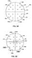
- the plate 172comprises two zones having at least one characteristic that is different from each other.
- the shieldmay comprise a number of zones with different configurations including various geometries (e.g., sizes, shapes and open areas), and the zones may be made of the same or different materials, or be adapted to have different potential bias.
- the spatial distribution of ions and neutrals in the plasmacan be modified in a localized manner, allowing customization of process characteristics such as etch uniformity, or locally enhanced or reduced etch rates (e.g., to tailor to different pattern densities in different parts of a mask), and so on.
- a multi-zone shieldfor example, can be used for active control of plasma species distribution, and thus, allow for enhanced process control.
- Figure 5Aillustrates one embodiment of a plate 172 having different zones 172A, 172B, 172C and 172D, with at least two zones being made of different materials.
- Suitable materialsinclude a variety of ceramics (e.g., alumina, yttria), anodized aluminum, quartz, materials with dielectric constant higher than about 4, e.g., K140 manufactured by Kyocera.
- These zonescan be provided in different geometric configurations or patterns, e.g., as wedges arranged in a circle (shown in Figures 5A ), in concentric rings, in a grid or slice pattern, or other combinations of different geometric shapes.
- Figure 5Billustrates another embodiment, where the plate 172 is made primarily of one material, but is divided into different zones or segments, 172A, 172B, 172C and 172D, that are physically separated or electrically isolated from each other. For example, zones of the same materials may be separated by a gap 172G, or by a different material. These zones are configured so that each can be independently biased to a different potential. As shown in Figure 5B , zones 172A and 172B connected to respective power sources, e.g., 190A, 190B, for supplying a potential bias, which can be independently controlled for each zone. Such connection may be provided through one of the support legs 176, as shown in Figure 5C .
- power sourcese.g., 190A, 190B
- Figure 5Dshows an example where the plate 172 is made of one material with a potential bias applied across two locations, 172X and 172Y, on the plate 172.
- the potential biasis applied by connecting voltage sources 190C and 190D to the respective locations.
- a platewhether made of a single material or different materials, may comprise different zone configurations, or be provided with different potential bias across the plate.
- the various zonesmay also be configured to tailor to specific mask patterns so that process characteristics can be customized to suit specific needs. Thus, if a mask has regions of different pattern densities or loading, the desired etch rates for these regions may be different from each other. In that case, it is possible to configure the zones or segments on the shield plate 172 based on the specific mask patterns in order to achieve the desired etch result.
- the apertures 174may generally have dimensions ranging from 0.03 inches (0.07 cm) to about 3 inches (7.62 cm), and may be arranged to define an open area within each zone of the plate 172 from about 2 percent to about 90 percent.
- the size, shape and patterning of the apertures 174may be varied according to the desired ion density in the lower process volume 180. For example, more apertures of small diameters in a particular zone of the plate 172 may be used to increase the radical (or neutral) to ion density ratio in a corresponding region of the volume 180. Alternatively, a number of larger apertures may be interspersed with small apertures to increase the ion to radical (or neutral) density ratio in a corresponding region of the volume 180.
- the height at which the ion-radical shield 170 is supportedmay vary to further control the etch process.
- a faster etch ratemay be obtained by locating the ion-radical shield 170 closer to the pedestal 124 and, therefore, the substrate 122.
- a lower, but more controlled, etch ratemay be obtained by locating the ion-radical shield 170 farther from the pedestal 124. Controlling the etch rate by adjusting the height of the ion-radical shield 170 thus allows balancing faster etch rates with improved critical dimension uniformity and reduced etch bias.
- the ion-radical shield 170may be positioned at different heights in chambers having different geometries, for example, larger or smaller chambers.
- the legs 176which support the plate 172 in a spaced-apart relationship with respect to the substrate 122, are generally located around an outer perimeter of the pedestal 124 or the edge ring 126 and may be fabricated of the same materials as the plate 172. In one embodiment, three legs 176 are used to support the ion-radical shield 170. Although the legs 176 generally maintain the plate 172 in a substantially parallel orientation relative to the substrate 122 or pedestal 124, an angled orientation may also be used by having legs 176 of varied lengths. The legs 176 may be secured to the plate 172 by a variety of fastening methods, and may be supported on the pedestal 124, adapter 182, or the edge ring 126.
- the plate 172may be supported above the pedestal 124 by other means such as by using a bracket (not shown) attached to the wall 104 or other structure within the process chamber 102. In these situations, the plate 172 is generally insulated from any ground path such as the ground 106.
- a deflector plate assembly 200is provided above the plate 172.
- the plate 172is absent and the deflector plate assembly 200 is disposed above the reticle adapter 182 and/or edge ring 126.
- the deflector plate assembly 200comprises a first plate 210 maintained in a spaced-apart relationship to the plate 172 by a first support assembly 202.
- the first plate 210can be fabricated from a variety of materials compatible with the processes, e.g., ceramic, quartz, or anodized aluminum.
- the first plate 210has an aperture 215 that changes the primary gas flow direction for the plasma gases entering the chamber 102 from gas inlets 116 towards the plate 172.
- the aperture 215is located at the center of the first plate 210, which is also aligned with the center of the shield plate 172.
- the aperture 215may be disposed at other locations on the first plate 210 in order to provide desired gas flow patterns to suit specific processing needs.
- additional aperturesmay be provided at various locations of the first plate 210, if desired. For example, apertures having smaller diameters compared to aperture 215 may be used to provide fine tuning of the gas flow pattern.
- the first support assembly 202may comprise one or more support members, e.g., a plurality of elongated members or legs, coupling the first plate 210 to the shield plate 172.
- the legsmay be attached to the shield plate 172 and the first plate 210 by a variety of conventional means, including screws, bolts, and so on.
- Figure 2is a schematic diagram of a top view of one embodiment of the first plate 210. In one embodiment, three legs are used to attach the first plate 210 to the shield plate 172, e.g., by threading the legs to mounting holes 212, 213, 214 on the first plate 210.
- the vertical distance between the first plate 210 and the shield plate 172may vary, depending on factors such as the chamber dimension, pumping configuration, gas flow requirements and specific process needs.
- the first plate 210is located at a distance of about 2 to 3 inches above the shield plate 172. In other embodiments, the separation distance may range from about 5 inches to about 6 inches.
- the deflector plate assembly 200further comprises a second plate 220 disposed above the first plate 210. As shown in Figure 1 , the second (or top) plate 220 is supported on the first (or bottom) plate 210 by a second support assembly 204.
- the top plate 220has a downwardly protruding portion 225 disposed proximate to the aperture 215 of the bottom plate 210. In one embodiment, the downwardly protruding portion 225 is located at the center of the top plate 220, and furthermore, is aligned laterally relative to the aperture 215, which has a diameter of about 50.8 mm (2 inches).
- FIG 3is a schematic illustration of a perspective bottom view of the top plate 220, showing the downwardly protruding portion 225 near the center.
- the top plate 220has three threaded holes 222, 224, 226 for coupling to respective support members of the second support assembly 204, which are attached at the other ends to the bottom plate 210 at mounting holes 216, 217, 218 (in Figure 2 ).
- the downwardly protruding portion 225generally has a cross-sectional shape similar to that of the aperture 215, e.g., a conical or truncated conical shape in the embodiment of Figure 3 .
- the protruding portion 225preferably has a taper towards the center, e.g., having one end (or the base) 227 at the plane of the plate 220 wider than a far or distal end 229, i.e., dimension d 1 being larger than d 2 .
- the top plate 220 and the bottom plate 210is separated by a distance of about 38.1 to 50.8 mm (1.5 to 2 inches), and the aperture 215 is a circle with a diameter of about 50.8 mm (2 inches).
- simulation resultsshow that a relatively focused vertical gas flow towards the shield and a perpendicular flow to the photomask substrate surface can be established with a side injection gas velocity ranging from about 5 m/s to about 20 m/s, although other velocities may also be used.
- One of the criteria for selecting certain gas flow velocities and deflector plate assembly dimensionsis that a relatively focused vertical gas flow be maintained perpendicular to the ion radical shield.
- the separation distancemay range from about 25.4 to 76.2 mm (1 to 3 inches), and the aperture diameter may range from about 25.4 to 76.2 mm (1 to 3 inches).
- the distances between the top plate 220, the bottom plate 210, and the shield plate 172, the degree of taper, shape or dimension of the protruding portion 225, as well as the shape, location and dimension of the aperture 215,may vary according to specific design and application needs, taking into considerations various factors such as the chamber dimension, pumping configuration, gas flow velocities, and so on. Aside from achieving certain desired etch rate or uniformity results, the design parameters are selected to provide a process with relatively wide margins.
- one or more process gasesare provided to the process chamber 102 from a gas panel 120, e.g., through one or more inlets 116 (e.g., openings, injectors, nozzles, and the like) located above the substrate pedestal 124.
- the gas inlets 116are disposed above the bottom plate 210 of the deflector plate assembly 200.
- the process gasesare provided to the inlets 116 using an annular gas channel 118, which may be formed in the wall 104 or in gas rings (as shown) that are coupled to the wall 104.
- the process gasescan be directed to flow primarily towards the center of the chamber 102, e.g., along the direction indicated by arrows 250.
- the process gasesflow in a lateral direction above the bottom plate 210, e.g., radially inwards from the side gas inlets 116, and downwards through the aperture 215 of the bottom plate 210 towards the shield plate 172.
- the gas inlets 116may also be provided in other locations of the chamber 102, e.g., at the lid 108 or be centrally located on the lid 108.
- the gas inlets 116are disposed at a vertical location at or below the top plate 220.
- the gas flow between the top plate 220 and the bottom plate 210e.g., in a radially inward direction, is deflected or re-directed by the downwardly protruding portion 225 through aperture 215.
- the radial velocities of gases entering the chamber 102the positions of the downwardly protruding portion 225 and the aperture 215, as well as the vertical locations of the top and bottom plates 220, 210, the spatial or lateral distribution of ions and neutral species passing through shield 170 can be controlled, which in turn, allows the etch rate profile to be tuned.
- the aperture 215is centrally located on the bottom plate 210 in this illustrative embodiment, it can also be disposed at other locations, or be provided with different shapes and dimensions, in order to establish desired flow patterns that are suitable for other application needs.
- the process gasesare ignited into a plasma by applying power from the plasma source 112 to the antenna 110.
- the pressure in the chamber 102is controlled using a throttle valve 162 and a vacuum pump 164.
- the temperature of the wall 104may be controlled using liquid-containing conduits (not shown) that run through the wall 104.
- the chamber wall 104is formed from a metal (e.g., aluminum, stainless steel, among others) and is coupled to an electrical ground 106.
- the process chamber 102also comprises conventional systems for process control, internal diagnostic, end point detection, and the like. Such systems are collectively shown as support systems 154.
- the controller 146comprises a central processing unit (CPU) 150, a memory 148, and support circuits 152 for the CPU 150 and facilitates control of the components of the process chamber 102 and, as such, of the etch process, as discussed below in further detail.
- the controller 146may be one of any form of general-purpose computer processor that can be used in an industrial setting for controlling various chambers and sub-processors.
- the memory, or computer-readable medium, of the CPU 150may be one or more of readily available memory such as random access memory (RAM), read only memory (ROM), floppy disk, hard disk, or any other form of digital storage, local or remote.
- the support circuits 152are coupled to the CPU 150 for supporting the processor in a conventional manner.
- circuitsinclude cache, power supplies, clock circuits, input/output circuitry and subsystems, and the like.
- the inventive methodis generally stored in the memory 148 as a software routine.
- such software routinemay also be stored and/or executed by a second CPU (not shown) that is remotely located from the hardware being controlled by the CPU 150.
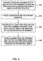
- Figure 4illustrates a method 400 that can be used for etching a photomask substrate in an etch chamber incorporating the herein described deflector plate assembly.
- the method 400begins at step 402 in which a process chamber is provided with a deflector plate assembly and an ion-neutral shield above a support pedestal.
- the deflector plate assemblyhas at least one aperture located above the shield.
- a substrateis placed on the support pedestal.
- Typical substratesgenerally comprise an optically transparent silicon based material, such as quartz (i.e., silicon dioxide, SiO 2 ), having an opaque light-shielding layer of metal disposed on the surface of the quartz.
- Typical metals used in a photomaskinclude chromium or chromium oxynitride.
- the substratemay also include a layer of silicon nitride (SiN) doped with molybdenum (Mo) interposed between the quartz and chromium.
- At step 406at least one process gas is introduced into the process chamber through a gas inlet located above the aperture of the deflector plate assembly.
- the direction of the process gas flow towards the shieldis partly defined by the aperture of the deflector plate assembly and the location of the gas inlets.
- a gas flowis established in a radially inward direction towards the aperture, e.g., by providing an appropriate flow velocity.
- a second plate having a downwardly protruding portionis provided above the first plate for re-directing the gas flow downwards towards the aperture.
- Exemplary process gasesmay include oxygen (O 2 ) or an oxygen-containing gas, such as carbon monoxide (CO), and/or a halogen-containing gas, such as a chlorine-containing gas for etching the metal layer.
- the processing gasmay further include an inert gas or another oxygen-containing gas.
- Carbon monoxideis advantageously used to form passivating polymer deposits on the surfaces, particularly the sidewalls, of openings and patterns formed in a patterned resist material and etched metal layers.
- Chlorine-containing gasesare selected from the group of chlorine (Cl 2 ), silicon tetrachloride (SiCl 4 ), boron trichloride (BCl 3 ), and combinations thereof, and are used to supply reactive radicals to etch the metal layer.
- the process gasesmay comprise a fluorine-containing gas, e.g., trifluoromethane (CHF 3 ), tetrafluoromethane (CF 4 ), among others.
- a fluorine-containing gase.g., trifluoromethane (CHF 3 ), tetrafluoromethane (CF 4 ), among others.
- a plasmais formed from the process gas in a process volume above the ion-radical shield, for example, by applying RF power from a plasma power source to an antenna.
- Ions and neutral speciespass through the ion-radical shield according to a distribution pattern resulting from a combination of the process gas flow direction (as defined by the deflector plate assembly) and the potentials across the ion-radical shield.
- the substrateis etched by the ions and neutral species in the lower process volume.
- the apparatuscan include a process chamber having a support pedestal adapted for receiving a photomask.
- An ion-neutral shieldcan be disposed above the pedestal and a deflector plate assembly can be provided above the ion-neutral shield.
- the deflector plate assemblycan define a gas flow direction for process gases towards the ion-neutral shield, while the ion-neutral shield is used to establish a desired distribution of ion and neutral species in a plasma for etching the photomask.
- the method and apparatus of the present inventioncan be used advantageously, for example, in an etch process that otherwise exhibits a radial nonuniformity such as one having a slower etch rate at the center compared to the edge.
- a gas flow direction or pattern or increasing the gas flow velocity in a predetermined regione.g., the center region
- the deflector plate assemblycan lead to an enhanced etch rate in a corresponding region of the photomask, and thus, result in improved etch uniformity.
- the flow velocities of one or more process gases in various applicationscan also be adjusted to achieve desired etch profile or process results.
Landscapes
- Engineering & Computer Science (AREA)
- Physics & Mathematics (AREA)
- Plasma & Fusion (AREA)
- Chemical & Material Sciences (AREA)
- Analytical Chemistry (AREA)
- General Physics & Mathematics (AREA)
- Condensed Matter Physics & Semiconductors (AREA)
- Manufacturing & Machinery (AREA)
- Computer Hardware Design (AREA)
- Microelectronics & Electronic Packaging (AREA)
- Power Engineering (AREA)
- Drying Of Semiconductors (AREA)
- Plasma Technology (AREA)
- Preparing Plates And Mask In Photomechanical Process (AREA)
Description
- Embodiments of the present invention generally relate to a method and apparatus for plasma etching photomasks and, more specifically, to a method and apparatus with improved control of distribution of plasma species.
- The fabrication of microelectronics or integrated circuit devices typically involves a complicated process sequence requiring hundreds of individual steps performed on semiconductive, dielectric and conductive substrates. Examples of these process steps include oxidation, diffusion, ion implantation, thin film deposition, cleaning, etching and lithography. Using lithography and etching (often referred to as pattern transfer steps), a desired pattern is first transferred to a photosensitive material layer, e.g., a photoresist, and then to the underlying material layer during subsequent etching. In the lithographic step, a blanket photoresist layer is exposed to a radiation source through a reticle or photomask containing a pattern so that an image of the pattern is formed in the photoresist. By developing the photoresist in a suitable chemical solution, portions of the photoresist are removed, thus resulting in a patterned photoresist layer. With this photoresist pattern acting as a mask, the underlying material layer is exposed to a reactive environment, e.g., using wet or dry etching, which results in the pattern being transferred to the underlying material layer.
- The pattern on a photomask, which is typically formed in a metal-containing layer supported on a glass or quartz substrate, is also generated by etching through a photoresist pattern. In this case, however, the photoresist pattern is created by a direct write technique, e.g., with an electron beam or other suitable radiation beam, as opposed to exposing the photoresist through a reticle. With the patterned photoresist as a mask, the pattern can be transferred to the underlying metal-containing layer using plasma etching. An example of a commercially available photomask etch equipment suitable for use in advanced device fabrication is the Tetra™ Photomask Etch System, available from Applied Materials, Inc., of Santa Clara, California. The terms "mask", "photomask" or "reticle" will be used interchangeably to denote generally a substrate containing a pattern.
- The US application
US 2003/0019580A1 refers to a method and an apparatus for tunable gas injection in a plasma processing system. The apparatus includes a gas injection manifold having a pressurizable plenum and an array of adjustable nozzle units, or an array of non-adjustable nozzles, through which gas from the plenum can flow into the interior region of a plasma reactor chamber capable of containing a plasma. The adjustable nozzle units include a nozzle plug arranged within a nozzle bore. A variety of different nozzle units are disclosed. The nozzle plugs are axially translatable to adjust the flow of gas therethrough. In one embodiment of the US applicationUS 2003/0019580A1 , the nozzle plugs are attached to a plug plate, which is displacable relative to an injection plate via displacement actuators connecting the two plates. The displacement actuators are controlled by a displacement actuator control unit, which is in electronic communication with a plasma processing system control unit. The gas flow into the chamber interior region is preferably controlled by monitoring the pressure in the plenum and in the chamber and adjusting the nozzle units accordingly. Where the nozzle units are not adjustable, a portion of the nozzles are sized to a first flow condition, and another portion of the nozzles are sized to a second flow condition - The EP application
EP 1 612 840 A2 described a method and apparatus for photomask plasma etching. The method of etching a photomask includes providing a process chamber having a substrate support pedestal adapted to receive a photomask substrate thereon. An ion-radical shield is disposed above the pedestal. A substrate is placed upon the pedestal beneath the ion-radical shield. A process gas is introduced into the process chamber and a plasma is formed from the process gas. The substrate is etched predominantly with radicals that pass through the shield. - The EP application
EP 0 7032 392 US 5 593 540 describes a plasma etching system and plasma etching method. The US patentUS 6 287 643 B1 refers to an apparatus and a method for injecting and modifying the gas concentration of a meta-stable or atomic species in a downstream plasma reactor. - With ever-decreasing device dimensions, the design and fabrication of photomasks for advanced technology becomes increasingly complex, and control of critical dimensions and process uniformity becomes increasingly more important. Therefore, there is an ongoing need for improved process monitor and control in photomask fabrication.
- In light of the above, an apparatus for plasma etching according to independent claim 1, and a method of etching a photomask according to independent claim 10 are provided.
- Further advantages, features, aspects and details of the invention are evident from the dependent claims, the description and the drawings.
- The present invention generally provides a method and apparatus for etching photomasks. One embodiment provides an apparatus for plasma etching that includes a process chamber having a plasma forming region, a substrate support pedestal disposed in the process chamber, an RF power source adapted for forming a plasma within the chamber in the plasma forming region, a shield disposed in the chamber above the pedestal and below a plasma forming region in the chamber, the shield configured to control a distribution of ionic and neutral species of the plasma wherein the shield includes a shield plate including two zones having at least one characteristic different from each other, the at least one characteristic being one of material or potential bias, wherein, when the characteristic of the two zones different from each other is potential bias, the two zones are physically separated or electrically isolated from each other, The apparatus further includes at least one gas inlet for providing a gas flow into the chamber, and a deflector plate assembly disposed above the substrate support pedestal and within the plasma forming region of the chamber, the deflector plate assembly including a first plate having an aperture formed therein and a second plate disposed above the first plate and having a downward protruding portion disposed proximate to the aperture in the first plate, wherein the deflector plate assembly redirects the gas flow in the process chamber and is configured to control radial and vertical components of a gas flow pattern between the gas inlet and the substrate support pedestal in response to changes in gas velocity.
- Another embodiment provides a method of etching a photomask in a process chamber that includes placing a photomask on a support pedestal, providing a shield above the support pedestal inside the chamber having a plasma forming region, the shield configured to control a distribution of ionic and neutral species of the plasma, wherein the shield comprises a shield plate comprising two zones having at least one characteristic different from each other, the at least one characteristic being one of material or potential bias, wherein, when the characteristic of the two zones different from each other is potential bias, the two zones are physically separated or electrically isolated from each other. The method further includes introducing a process gas into the process chamber through at least one inlet, providing a predetermined gas flow pattern between the gas inlet and the shield by disposing a deflector plate assembly above the shield and within the plasma forming region, wherein the deflector plate assembly redirects the flow of process gas in the process chamber by a first plate with an aperture and a second plate having a downward protrusion disposed above the first plate, the downward protruding portion being proximate to the aperture in the first plate. The method further includes forming a plasma from the process gas in a region above the shield, and etching the photomask with ions and neutral species passing through the shield.
- In another example, which may be helpful for understanding, a method of etching a photomask in a process chamber is described that includes providing a shield above a support pedestal inside the chamber for controlling ions and neutral species passing through the shield, introducing a process gas into the process chamber through at least one inlet at a first flow velocity, providing a deflector plate assembly above the shield, the deflector plate assembly configured to provide a predetermined gas flow pattern between the gas inlet and the shield, placing a photomask on the support pedestal, forming a plasma from the process gas, etching a first photomask at the first flow velocity, obtaining an etch rate profile based on the etched first substrate, adjusting the process gas through the at least one inlet to a second flow velocity based on the etch rate profile, and etching a second photomask at the second flow velocity.
- Embodiments are also directed to apparatuses for carrying out the disclosed methods and including apparatus parts for performing described method steps. Furthermore, embodiments are also directed to methods by which the described apparatus operates or by which the described apparatus is manufactured. It may include method steps for carrying out functions of the apparatus or manufacturing parts of the apparatus. The method steps may be performed by way of hardware component, firmware, a computer programmed by appropriate software, by any combination thereof or in any other manner.
- So that the manner in which the above recited features of the present invention can be understood in detail, a more particular description of the invention, briefly summarized above, may be had by reference to embodiments, some of which are illustrated in the appended drawings. It is to be noted, however, that the appended drawings illustrate only typical embodiments of this invention and are therefore not to be considered limiting of its scope, for the invention may admit to other equally effective embodiments.
- The invention is defined by the claims.
Figure 1 is a schematic diagram of a plasma process chamber with a deflector plate assembly of the present invention;Figure 2 is a schematic diagram of a top view of one embodiment of a plate in the deflector plate assembly ofFigure 1 ;Figure 3 is a schematic diagram of a perspective view of one embodiment of a second plate in the deflector plate assembly ofFigure 1 ;Figure 4 is a flow chart of a method of etching a photomask; andFigures 5A-5C illustrate schematically different embodiments of an ion-neutral shield that can be used in conjunction with the deflector plate assembly.Figure 5D shows an example of an ion-neutral shield.- To facilitate understanding, identical reference numerals have been used, where possible, to designate identical elements that are common to the figures. It is contemplated that elements and features of one embodiment may be beneficially incorporated in other embodiments without further recitation.
- It is to be noted, however, that the appended drawings illustrate only exemplary embodiments of this invention and are therefore not to be considered limiting of its scope, for the invention may admit to other equally effective embodiments.
- The present invention provides a method and apparatus for etching of a photomask substrate by providing improved control of the gas flow pattern and plasma uniformity. The apparatus includes a deflector plate assembly configured to control the radial and vertical components of a gas flow provided in the processing chamber. The deflector plate assembly is disposed above the substrate. A shield, also referred to as an ion-radical shield or ion-neutral shield, is disposed between the deflector plate assembly and the substrate. A plasma is formed in a quasi-remote, upper processing region of the chamber above the shield, which is configured for controlling the distribution of charged and neutral species in the chamber during processing.
- In another embodiment, the deflector plate assembly is used to redirect the flow of gases in the processing chamber. The deflector plate assembly comprises a first plate having an aperture, whose location and dimension help define a primary direction of gas flow towards the shield. The deflector plate assembly further comprises a second plate disposed above the first plate. The second plate has a downwardly protruding portion that is substantially aligned with the aperture of the first plate. A gas flowing in a lateral direction, approximately parallel the first plate and the second plate, is deflected by the downwardly protruding portion and redirected through the aperture of the first plate. By establishing a primary gas flow direction or pattern or increasing the gas flow velocity in a predetermined region, the deflector plate assembly can lead to an enhanced etch rate in a predetermined location, and thus, result in improved etch uniformity.
- Examples of an ion-radical shield for use in a plasma etch chamber have been disclosed in
U.S. Patent Application S/N 10/880,754 U.S. Patent Application S/N 11/554,495 Figure 1 depicts a schematic diagram of anetch reactor 100 having an ion-radical shield 170. Suitable reactors that may be adapted for use with the teachings disclosed herein include, for example, the Decoupled Plasma Source (DPS®) II reactor, or the Tetra™ I and Tetra™ II Photomask etch systems, all of which are available from Applied Materials, Inc. of Santa Clara, California. The particular embodiment of thereactor 100 shown herein is provided for illustrative purposes and should not be used to limit the scope of the invention. It is contemplated that the invention may be utilized in other processing systems, including those from other manufacturers.- The
reactor 100 generally comprises aprocess chamber 102 having asubstrate pedestal 124 within a conductive body (wall) 104, and acontroller 146. Thechamber 102 has a substantially flat dielectric ceiling orlid 108. Other modifications of thechamber 102 may have other types of ceilings, e.g., a dome-shaped ceiling. Anantenna 110 is disposed above theceiling 108 and comprises one or more inductive coil elements that may be selectively controlled (twoco-axial elements Figure 1 ). Theantenna 110 is coupled through afirst matching network 114 to aplasma power source 112, which is typically capable of producing up to about 3000 W at a tunable frequency in a range from about 50 kHz to about 13.56 MHz. - Processing gases are provided into the
chamber 102 through one ormore inlets 116 from agas panel 120. Theinlets 116 may be located on thelid 108 orwall 104 of thechamber 102. In the embodiment depicted inFigure 1 , theinlets 116 are positioned to induce a predominantly radial flow of gases entering thechamber 102, for example, throughinlets 116 formed in thewalls 104 of thechamber 102. - The substrate pedestal (cathode) 124 is coupled through a
second matching network 142 to a biasingpower source 140. The biasingsource 140 generally is a source of up to about 500 W at a frequency of approximately 13.56 MHz that is capable of producing either continuous or pulsed power. Alternatively, thesource 140 may be a DC or pulsed DC source. In one embodiment, thesubstrate support pedestal 124 comprises anelectrostatic chuck 160, which has at least oneclamping electrode 132 and is controlled by achuck power supply 166. In alternative embodiments, thesubstrate pedestal 124 may comprise substrate retention mechanisms such as a susceptor clamp ring, a mechanical chuck, and the like. - A
reticle adapter 182 is used to secure the substrate (e.g., mask or reticle) 122 onto thesubstrate support pedestal 124. Thereticle adapter 182 generally includes alower portion 184 that covers an upper surface of the pedestal 124 (for example, the electrostatic chuck 160) and atop portion 186 having anopening 188 that is sized and shaped to hold thesubstrate 122. Theopening 188 is generally substantially centered with respect to thepedestal 124. Theadapter 182 is generally formed from a single piece of etch resistant, high temperature resistant material such as polyimide ceramic or quartz. Anedge ring 126 may cover and/or secure theadapter 182 to thepedestal 124. Alift mechanism 138 is used to lower or raise theadapter 182, and hence, thesubstrate 122, onto or off of thesubstrate support pedestal 124. Generally, thelift mechanism 162 comprises a plurality of lift pins 130 (one lift pin is shown) that travel through respective guide holes 136. - In operation, the temperature of the
substrate 122 is controlled by stabilizing the temperature of thesubstrate pedestal 124. In one embodiment, thesubstrate support pedestal 124 comprises aresistive heater 144 and aheat sink 128. Theresistive heater 144 generally comprises at least oneheating element 134 and is regulated by aheater power supply 168. A backside gas, e.g., helium (He), from agas source 156 is provided via agas conduit 158 to channels that are formed in the pedestal surface under thesubstrate 122 to facilitate heat transfer between thepedestal 124 and thesubstrate 122. During processing, thepedestal 124 may be heated by theresistive heater 144 to a steady-state temperature, which in combination with the backside gas, facilitates uniform heating of thesubstrate 122. Using such thermal control, thesubstrate 122 may be maintained at a temperature between about 0 and 350 degrees Celsius (°C). - An ion-
radical shield 170 is disposed in thechamber 102 above thepedestal 124. The ion-radical shield 170 is electrically isolated from thechamber walls 104 and thepedestal 124 such that no ground path from the plate to ground is provided. One embodiment of the ion-radical shield 170 comprises a substantiallyflat plate 172 and a plurality oflegs 176 supporting theplate 172. Theplate 172, which may be made of a variety of materials compatible with process needs, comprises one or more openings (apertures) 174 that define a desired open area in theplate 172. This open area controls the amount of ions that pass from a plasma formed in anupper process volume 178 of theprocess chamber 102 to alower process volume 180 located between the ion-radical shield 170 and thesubstrate 122. The greater the open area, the more ions can pass through the ion-radical shield 170. As such, the size of theapertures 174 controls the ion density involume 180, and theshield 170 serves as an ion filter. Theplate 172 may also comprise a screen or a mesh wherein the open area of the screen or mesh corresponds to the desired open area provided byapertures 174. Alternatively, a combination of a plate and screen or mesh may also be used. - During processing, a potential develops on the surface of the
plate 172 as a result of electron bombardment from the plasma. The potential attracts ions from the plasma, effectively filtering them from the plasma, while allowing neutral species, e.g., radicals, to pass through theapertures 174 of theplate 172. Thus, by reducing the amount of ions through the ion-radical shield 170, etching of the mask by neutral species or radicals can proceed in a more controlled manner. This reduces erosion of the resist as well as sputtering of the resist onto the sidewalls of the patterned material layer, thus resulting in improved etch bias and critical dimension uniformity. - Different combinations of materials and/or configurations are provided in various embodiments of the
shield plate 172. In one embodiment, theplate 172 may be made of a materials having a dielectric constant greater than about 4, including for example, ceramics such as alumina, yttria and K140 (a proprietary material available from Kyocera). Theplate 172 comprises two zones having at least one characteristic that is different from each other. For example, the shield may comprise a number of zones with different configurations including various geometries (e.g., sizes, shapes and open areas), and the zones may be made of the same or different materials, or be adapted to have different potential bias. By providing combinations of zone configurations, materials and/or potential bias, the spatial distribution of ions and neutrals in the plasma can be modified in a localized manner, allowing customization of process characteristics such as etch uniformity, or locally enhanced or reduced etch rates (e.g., to tailor to different pattern densities in different parts of a mask), and so on. Such a multi-zone shield, for example, can be used for active control of plasma species distribution, and thus, allow for enhanced process control. Figure 5A illustrates one embodiment of aplate 172 havingdifferent zones Figures 5A ), in concentric rings, in a grid or slice pattern, or other combinations of different geometric shapes.Figure 5B illustrates another embodiment, where theplate 172 is made primarily of one material, but is divided into different zones or segments, 172A, 172B, 172C and 172D, that are physically separated or electrically isolated from each other. For example, zones of the same materials may be separated by agap 172G, or by a different material. These zones are configured so that each can be independently biased to a different potential. As shown inFigure 5B ,zones support legs 176, as shown inFigure 5C .Figure 5D shows an example where theplate 172 is made of one material with a potential bias applied across two locations, 172X and 172Y, on theplate 172. The potential bias is applied by connectingvoltage sources locations plate 172 betweenlocations - These various embodiments and the example of the
plate 172 can be used in combination with each other, e.g., a plate, whether made of a single material or different materials, may comprise different zone configurations, or be provided with different potential bias across the plate. The various zones may also be configured to tailor to specific mask patterns so that process characteristics can be customized to suit specific needs. Thus, if a mask has regions of different pattern densities or loading, the desired etch rates for these regions may be different from each other. In that case, it is possible to configure the zones or segments on theshield plate 172 based on the specific mask patterns in order to achieve the desired etch result. - The
apertures 174, which may vary in size, shape, spacing and geometric arrangement, may generally have dimensions ranging from 0.03 inches (0.07 cm) to about 3 inches (7.62 cm), and may be arranged to define an open area within each zone of theplate 172 from about 2 percent to about 90 percent. The size, shape and patterning of theapertures 174 may be varied according to the desired ion density in thelower process volume 180. For example, more apertures of small diameters in a particular zone of theplate 172 may be used to increase the radical (or neutral) to ion density ratio in a corresponding region of thevolume 180. Alternatively, a number of larger apertures may be interspersed with small apertures to increase the ion to radical (or neutral) density ratio in a corresponding region of thevolume 180. - The height at which the ion-
radical shield 170 is supported may vary to further control the etch process. The closer the ion-radical shield 170 is located to theceiling 108, the smaller theupper process volume 178, which tends to promote a more stable plasma. A faster etch rate may be obtained by locating the ion-radical shield 170 closer to thepedestal 124 and, therefore, thesubstrate 122. Alternatively, a lower, but more controlled, etch rate may be obtained by locating the ion-radical shield 170 farther from thepedestal 124. Controlling the etch rate by adjusting the height of the ion-radical shield 170 thus allows balancing faster etch rates with improved critical dimension uniformity and reduced etch bias. It is contemplated that the ion-radical shield 170 may be positioned at different heights in chambers having different geometries, for example, larger or smaller chambers. - The
legs 176, which support theplate 172 in a spaced-apart relationship with respect to thesubstrate 122, are generally located around an outer perimeter of thepedestal 124 or theedge ring 126 and may be fabricated of the same materials as theplate 172. In one embodiment, threelegs 176 are used to support the ion-radical shield 170. Although thelegs 176 generally maintain theplate 172 in a substantially parallel orientation relative to thesubstrate 122 orpedestal 124, an angled orientation may also be used by havinglegs 176 of varied lengths. Thelegs 176 may be secured to theplate 172 by a variety of fastening methods, and may be supported on thepedestal 124,adapter 182, or theedge ring 126. - Alternatively, the
plate 172 may be supported above thepedestal 124 by other means such as by using a bracket (not shown) attached to thewall 104 or other structure within theprocess chamber 102. In these situations, theplate 172 is generally insulated from any ground path such as theground 106. - According to one embodiment of the present invention, a
deflector plate assembly 200 is provided above theplate 172. In an example useful for understanding the embodiments, theplate 172 is absent and thedeflector plate assembly 200 is disposed above thereticle adapter 182 and/oredge ring 126. In one embodiment, thedeflector plate assembly 200 comprises afirst plate 210 maintained in a spaced-apart relationship to theplate 172 by afirst support assembly 202. Thefirst plate 210 can be fabricated from a variety of materials compatible with the processes, e.g., ceramic, quartz, or anodized aluminum. As shown in a schematic cross-section view inFigure 1 , thefirst plate 210 has anaperture 215 that changes the primary gas flow direction for the plasma gases entering thechamber 102 fromgas inlets 116 towards theplate 172. In one embodiment, theaperture 215 is located at the center of thefirst plate 210, which is also aligned with the center of theshield plate 172. In other embodiments, theaperture 215 may be disposed at other locations on thefirst plate 210 in order to provide desired gas flow patterns to suit specific processing needs. Furthermore, additional apertures may be provided at various locations of thefirst plate 210, if desired. For example, apertures having smaller diameters compared toaperture 215 may be used to provide fine tuning of the gas flow pattern. - The
first support assembly 202 may comprise one or more support members, e.g., a plurality of elongated members or legs, coupling thefirst plate 210 to theshield plate 172. The legs may be attached to theshield plate 172 and thefirst plate 210 by a variety of conventional means, including screws, bolts, and so on.Figure 2 is a schematic diagram of a top view of one embodiment of thefirst plate 210. In one embodiment, three legs are used to attach thefirst plate 210 to theshield plate 172, e.g., by threading the legs to mountingholes first plate 210. The vertical distance between thefirst plate 210 and theshield plate 172 may vary, depending on factors such as the chamber dimension, pumping configuration, gas flow requirements and specific process needs. In one embodiment, thefirst plate 210 is located at a distance of about 2 to 3 inches above theshield plate 172. In other embodiments, the separation distance may range from about 5 inches to about 6 inches. - The
deflector plate assembly 200 further comprises asecond plate 220 disposed above thefirst plate 210. As shown inFigure 1 , the second (or top)plate 220 is supported on the first (or bottom)plate 210 by asecond support assembly 204. Thetop plate 220 has a downwardly protrudingportion 225 disposed proximate to theaperture 215 of thebottom plate 210. In one embodiment, the downwardly protrudingportion 225 is located at the center of thetop plate 220, and furthermore, is aligned laterally relative to theaperture 215, which has a diameter of about 50.8 mm (2 inches). Figure 3 is a schematic illustration of a perspective bottom view of thetop plate 220, showing the downwardly protrudingportion 225 near the center. In this embodiment, thetop plate 220 has three threadedholes second support assembly 204, which are attached at the other ends to thebottom plate 210 at mountingholes Figure 2 ). The downwardly protrudingportion 225 generally has a cross-sectional shape similar to that of theaperture 215, e.g., a conical or truncated conical shape in the embodiment ofFigure 3 . The protrudingportion 225 preferably has a taper towards the center, e.g., having one end (or the base) 227 at the plane of theplate 220 wider than a far ordistal end 229, i.e., dimension d1 being larger than d2.- In one embodiment, the
top plate 220 and thebottom plate 210 is separated by a distance of about 38.1 to 50.8 mm (1.5 to 2 inches), and theaperture 215 is a circle with a diameter of about 50.8 mm (2 inches). For this configuration, simulation results show that a relatively focused vertical gas flow towards the shield and a perpendicular flow to the photomask substrate surface can be established with a side injection gas velocity ranging from about 5 m/s to about 20 m/s, although other velocities may also be used. One of the criteria for selecting certain gas flow velocities and deflector plate assembly dimensions is that a relatively focused vertical gas flow be maintained perpendicular to the ion radical shield. In other embodiments, the separation distance may range from about 25.4 to 76.2 mm (1 to 3 inches), and the aperture diameter may range from about 25.4 to 76.2 mm (1 to 3 inches). In general, the distances between thetop plate 220, thebottom plate 210, and theshield plate 172, the degree of taper, shape or dimension of the protrudingportion 225, as well as the shape, location and dimension of theaperture 215, may vary according to specific design and application needs, taking into considerations various factors such as the chamber dimension, pumping configuration, gas flow velocities, and so on. Aside from achieving certain desired etch rate or uniformity results, the design parameters are selected to provide a process with relatively wide margins. - Prior to plasma etching, one or more process gases are provided to the
process chamber 102 from agas panel 120, e.g., through one or more inlets 116 (e.g., openings, injectors, nozzles, and the like) located above thesubstrate pedestal 124. In the embodiment ofFigure 1 , thegas inlets 116 are disposed above thebottom plate 210 of thedeflector plate assembly 200. As shown inFigure 1 , the process gases are provided to theinlets 116 using anannular gas channel 118, which may be formed in thewall 104 or in gas rings (as shown) that are coupled to thewall 104. By appropriate choice of the gas flow velocities, the location of thedeflector plate assembly 200, and the size ofaperture 215, the process gases can be directed to flow primarily towards the center of thechamber 102, e.g., along the direction indicated byarrows 250. Thus, the process gases flow in a lateral direction above thebottom plate 210, e.g., radially inwards from theside gas inlets 116, and downwards through theaperture 215 of thebottom plate 210 towards theshield plate 172. In alternative embodiments in which only thefirst plate 210 is used, thegas inlets 116 may also be provided in other locations of thechamber 102, e.g., at thelid 108 or be centrally located on thelid 108. - When the
top plate 220 is used, thegas inlets 116 are disposed at a vertical location at or below thetop plate 220. In this embodiment, the gas flow between thetop plate 220 and thebottom plate 210, e.g., in a radially inward direction, is deflected or re-directed by the downwardly protrudingportion 225 throughaperture 215. By adjusting the radial velocities of gases entering thechamber 102, the positions of the downwardly protrudingportion 225 and theaperture 215, as well as the vertical locations of the top andbottom plates shield 170 can be controlled, which in turn, allows the etch rate profile to be tuned. Although theaperture 215 is centrally located on thebottom plate 210 in this illustrative embodiment, it can also be disposed at other locations, or be provided with different shapes and dimensions, in order to establish desired flow patterns that are suitable for other application needs. During an etch process, the process gases are ignited into a plasma by applying power from theplasma source 112 to theantenna 110. - The pressure in the
chamber 102 is controlled using athrottle valve 162 and avacuum pump 164. The temperature of thewall 104 may be controlled using liquid-containing conduits (not shown) that run through thewall 104. Typically, thechamber wall 104 is formed from a metal (e.g., aluminum, stainless steel, among others) and is coupled to anelectrical ground 106. Theprocess chamber 102 also comprises conventional systems for process control, internal diagnostic, end point detection, and the like. Such systems are collectively shown assupport systems 154. - The
controller 146 comprises a central processing unit (CPU) 150, amemory 148, and supportcircuits 152 for theCPU 150 and facilitates control of the components of theprocess chamber 102 and, as such, of the etch process, as discussed below in further detail. Thecontroller 146 may be one of any form of general-purpose computer processor that can be used in an industrial setting for controlling various chambers and sub-processors. The memory, or computer-readable medium, of theCPU 150 may be one or more of readily available memory such as random access memory (RAM), read only memory (ROM), floppy disk, hard disk, or any other form of digital storage, local or remote. Thesupport circuits 152 are coupled to theCPU 150 for supporting the processor in a conventional manner. These circuits include cache, power supplies, clock circuits, input/output circuitry and subsystems, and the like. The inventive method is generally stored in thememory 148 as a software routine. Alternatively, such software routine may also be stored and/or executed by a second CPU (not shown) that is remotely located from the hardware being controlled by theCPU 150. Figure 4 illustrates a method 400 that can be used for etching a photomask substrate in an etch chamber incorporating the herein described deflector plate assembly. The method 400 begins atstep 402 in which a process chamber is provided with a deflector plate assembly and an ion-neutral shield above a support pedestal. The deflector plate assembly has at least one aperture located above the shield.- At
step 404, a substrate is placed on the support pedestal. Typical substrates generally comprise an optically transparent silicon based material, such as quartz (i.e., silicon dioxide, SiO2), having an opaque light-shielding layer of metal disposed on the surface of the quartz. Typical metals used in a photomask include chromium or chromium oxynitride. The substrate may also include a layer of silicon nitride (SiN) doped with molybdenum (Mo) interposed between the quartz and chromium. - At
step 406, at least one process gas is introduced into the process chamber through a gas inlet located above the aperture of the deflector plate assembly. The direction of the process gas flow towards the shield is partly defined by the aperture of the deflector plate assembly and the location of the gas inlets. For embodiments where gas inlets are provided around the perimeter region of the chamber, a gas flow is established in a radially inward direction towards the aperture, e.g., by providing an appropriate flow velocity. A second plate having a downwardly protruding portion is provided above the first plate for re-directing the gas flow downwards towards the aperture. - Exemplary process gases may include oxygen (O2) or an oxygen-containing gas, such as carbon monoxide (CO), and/or a halogen-containing gas, such as a chlorine-containing gas for etching the metal layer. The processing gas may further include an inert gas or another oxygen-containing gas. Carbon monoxide is advantageously used to form passivating polymer deposits on the surfaces, particularly the sidewalls, of openings and patterns formed in a patterned resist material and etched metal layers. Chlorine-containing gases are selected from the group of chlorine (Cl2), silicon tetrachloride (SiCl4), boron trichloride (BCl3), and combinations thereof, and are used to supply reactive radicals to etch the metal layer. In other embodiments such as those for etching quartz or MoSi, the process gases may comprise a fluorine-containing gas, e.g., trifluoromethane (CHF3), tetrafluoromethane (CF4), among others.
- At
step 408, a plasma is formed from the process gas in a process volume above the ion-radical shield, for example, by applying RF power from a plasma power source to an antenna. Ions and neutral species pass through the ion-radical shield according to a distribution pattern resulting from a combination of the process gas flow direction (as defined by the deflector plate assembly) and the potentials across the ion-radical shield. The substrate is etched by the ions and neutral species in the lower process volume. - According to some embodiments, methods and apparatuses for etching photomasks are provided. For example, in some embodiments, the apparatus can include a process chamber having a support pedestal adapted for receiving a photomask. An ion-neutral shield can be disposed above the pedestal and a deflector plate assembly can be provided above the ion-neutral shield. The deflector plate assembly can define a gas flow direction for process gases towards the ion-neutral shield, while the ion-neutral shield is used to establish a desired distribution of ion and neutral species in a plasma for etching the photomask.
- The method and apparatus of the present invention can be used advantageously, for example, in an etch process that otherwise exhibits a radial nonuniformity such as one having a slower etch rate at the center compared to the edge. By establishing a gas flow direction or pattern or increasing the gas flow velocity in a predetermined region, e.g., the center region, the deflector plate assembly can lead to an enhanced etch rate in a corresponding region of the photomask, and thus, result in improved etch uniformity. For a given deflector plate assembly configuration within a chamber, the flow velocities of one or more process gases in various applications can also be adjusted to achieve desired etch profile or process results.
- While the foregoing is directed to embodiments of the present invention, other and further embodiments of the invention may be devised without departing from the basic scope thereof, and the scope thereof is determined by the claims that follow.
Claims (11)
- An apparatus for plasma etching, comprising:a process chamber (102) having a plasma forming region (178);a substrate support pedestal (124) disposed in the process chamber;an RF power source (112) adapted for forming a plasma within the chamber in the plasma forming region (178);a shield (170) disposed in the process chamber (102) above the substrate support pedestal and below the plasma forming region (178) in the chamber, the shield configured to control a distribution of ionic and neutral species of the plasma, wherein the shield comprises a shield plate (172) comprising two zones having at least one characteristic different from each other, the at least one characteristic being one of material or potential bias, wherein, when the characteristic of the two zones different from each other is potential bias, the two zones are physically separated or electrically isolated from each other;at least one gas inlet (116) for providing a gas flow into the chamber; anda deflector plate assembly (200) disposed above the substrate support pedestal and within the plasma forming region (178) of the chamber, the deflector plate assembly comprising a first plate (210) having an aperture (215) formed therein and a second plate (220) disposed above the first plate and having a downward protruding portion (225) disposed proximate to the aperture (215) in the first plate, wherein the deflector plate assembly redirects the gas flow in the process chamber and is configured to control radial and vertical components of a gas flow pattern between the gas inlet and the substrate support pedestal in response to changes in gas velocity.
- The apparatus of claim 1, wherein the at least one gas inlet is disposed in a sidewall of the process chamber for producing a radial gas flow.
- The apparatus of any of claims 1 to 2, wherein the aperture is located in a central region of the first plate and the at least one gas inlet is disposed above the first plate.
- The apparatus of claim 1, wherein the downwardly protruding portion is substantially aligned with the aperture of the first plate and the downwardly protruding portion has a first end at a plane of the second plate and a distal end (229), the first end having a lateral dimension that is larger than a lateral dimension at the distal end.
- The apparatus of any of claims 1 to 4, wherein the deflector plate assembly is fabricated from at least one of ceramic, quartz, or anodized aluminum.
- The apparatus of any of claims 1 to 5, wherein the support pedestal is configured for supporting a photomask.
- The apparatus of any of claims 1 to 6,
wherein the aperture is located at a center of the first plate and substantially aligned with a center of the shield (170). - The apparatus of claim 7, wherein the first plate (210) of the deflector plate assembly (200) is attached to the shield (170) by a support assembly (202) and supported in a substantially parallel, spaced apart relation with respect to the shield.
- The apparatus of any claims 1 to 8, wherein each of the two zones comprises a material with a dielectric constant different from each other, the material being selected from the group consisting of anodized aluminum, ceramics, alumina, yttria, and materials having a dielectric constant higher than about 4.
- A method of etching a photomask in a process chamber, comprising:placing a photomask on a support pedestal (124);providing a shield (170) above the support pedestal inside the chamber having a plasma forming region (178), the shield configured to control a distribution of ionic and neutral species of the plasma, wherein the shield comprises a shield plate (172) comprising two zones having at least one characteristic different from each other, the at least one characteristic being one of material or potential bias, wherein, when the characteristic of the two zones different from each other is potential bias, the two zones are physically separated or electrically isolated from each other;introducing a process gas into the process chamber through at least one inlet (116);providing a predetermined gas flow pattern between the gas inlet and the shield by disposing a deflector plate assembly (200) above the shield and within the plasma forming region (178), wherein the deflector plate assembly redirects the flow of process gas in the process chamber by a first plate (210) with an aperture (215) and a second plate (220) having a downward protrusion disposed above the first plate (210), the downward protruding portion being proximate to the aperture (215) in the first plate (210);forming a plasma from the process gas in a region above the shield (170); andetching the photomask with ions and neutral species passing through the shield (170).
- The method of claim 10, wherein the step of providing a predetermined gas flow pattern further comprises:providing the deflector plate assembly with the first plate (210) disposed below the at least one inlet, the first plate comprising an aperture (215); anddirecting a gas flow through the aperture (215) towards the shield (170).
Applications Claiming Priority (1)
| Application Number | Priority Date | Filing Date | Title |
|---|---|---|---|
| US11/554,502US7943005B2 (en) | 2006-10-30 | 2006-10-30 | Method and apparatus for photomask plasma etching |
Publications (2)
| Publication Number | Publication Date |
|---|---|
| EP1918970A1 EP1918970A1 (en) | 2008-05-07 |
| EP1918970B1true EP1918970B1 (en) | 2016-09-21 |
Family
ID=39040307
Family Applications (1)
| Application Number | Title | Priority Date | Filing Date |
|---|---|---|---|
| EP07020930.9ANot-in-forceEP1918970B1 (en) | 2006-10-30 | 2007-10-25 | Method and apparatus for photomask plasma etching |
Country Status (6)
| Country | Link |
|---|---|
| US (2) | US7943005B2 (en) |
| EP (1) | EP1918970B1 (en) |
| JP (1) | JP5248839B2 (en) |
| KR (2) | KR100984422B1 (en) |
| CN (1) | CN101174107B (en) |
| TW (1) | TWI407503B (en) |
Families Citing this family (205)
| Publication number | Priority date | Publication date | Assignee | Title |
|---|---|---|---|---|
| US20060000802A1 (en)* | 2004-06-30 | 2006-01-05 | Ajay Kumar | Method and apparatus for photomask plasma etching |
| US8349128B2 (en)* | 2004-06-30 | 2013-01-08 | Applied Materials, Inc. | Method and apparatus for stable plasma processing |
| US7943005B2 (en)* | 2006-10-30 | 2011-05-17 | Applied Materials, Inc. | Method and apparatus for photomask plasma etching |
| US7909961B2 (en)* | 2006-10-30 | 2011-03-22 | Applied Materials, Inc. | Method and apparatus for photomask plasma etching |
| TWI404165B (en)* | 2007-04-02 | 2013-08-01 | Sosul Co Ltd | Apparatus for supporting substrate and plasma etching apparatus having the same |
| US20090120368A1 (en)* | 2007-11-08 | 2009-05-14 | Applied Materials, Inc. | Rotating temperature controlled substrate pedestal for film uniformity |
| US20090120584A1 (en)* | 2007-11-08 | 2009-05-14 | Applied Materials, Inc. | Counter-balanced substrate support |
| US20090277587A1 (en)* | 2008-05-09 | 2009-11-12 | Applied Materials, Inc. | Flowable dielectric equipment and processes |
| DE102008027856A1 (en) | 2008-06-11 | 2009-12-24 | W. L. Gore & Associates Gmbh | Shoe with ventilation in the lower shaft area and air-permeable spacer construction |
| US8329055B2 (en)* | 2008-10-02 | 2012-12-11 | Varian Semiconductor Equipment Associates, Inc. | Plasma uniformity control using biased array |
| US8834732B2 (en)* | 2008-10-02 | 2014-09-16 | Varian Semiconductor Equipment Associates, Inc. | Plasma uniformity control using biased array |
| US8980382B2 (en) | 2009-12-02 | 2015-03-17 | Applied Materials, Inc. | Oxygen-doping for non-carbon radical-component CVD films |
| US8741788B2 (en) | 2009-08-06 | 2014-06-03 | Applied Materials, Inc. | Formation of silicon oxide using non-carbon flowable CVD processes |
| KR200479181Y1 (en)* | 2009-09-10 | 2015-12-30 | 램 리써치 코포레이션 | Replaceable upper chamber parts of plasma processing apparatus |
| TWI385272B (en)* | 2009-09-25 | 2013-02-11 | Ind Tech Res Inst | Gas distribution plate and apparatus using the same |
| JP2013516763A (en)* | 2009-12-30 | 2013-05-13 | アプライド マテリアルズ インコーポレイテッド | Dielectric film growth using radicals generated using a flexible nitrogen / hydrogen ratio |
| JP2013521650A (en) | 2010-03-05 | 2013-06-10 | アプライド マテリアルズ インコーポレイテッド | Conformal layer by radical component CVD |
| US9324576B2 (en) | 2010-05-27 | 2016-04-26 | Applied Materials, Inc. | Selective etch for silicon films |
| US9793126B2 (en) | 2010-08-04 | 2017-10-17 | Lam Research Corporation | Ion to neutral control for wafer processing with dual plasma source reactor |
| AU2011293560B2 (en)* | 2010-08-23 | 2015-05-28 | Exogenesis Corporation | Method and apparatus for neutral beam processing based on gas cluster ion beam technology |
| US10202684B2 (en) | 2010-08-23 | 2019-02-12 | Exogenesis Corporation | Method for neutral beam processing based on gas cluster ion beam technology and articles produced thereby |
| US9285168B2 (en) | 2010-10-05 | 2016-03-15 | Applied Materials, Inc. | Module for ozone cure and post-cure moisture treatment |
| US8664127B2 (en) | 2010-10-15 | 2014-03-04 | Applied Materials, Inc. | Two silicon-containing precursors for gapfill enhancing dielectric liner |
| KR101992702B1 (en)* | 2010-10-28 | 2019-06-25 | 어플라이드 머티어리얼스, 인코포레이티드 | High purity aluminum coating hard anodization |
| US8741778B2 (en) | 2010-12-14 | 2014-06-03 | Applied Materials, Inc. | Uniform dry etch in two stages |
| US20120180954A1 (en)* | 2011-01-18 | 2012-07-19 | Applied Materials, Inc. | Semiconductor processing system and methods using capacitively coupled plasma |
| US10283321B2 (en) | 2011-01-18 | 2019-05-07 | Applied Materials, Inc. | Semiconductor processing system and methods using capacitively coupled plasma |
| US8771539B2 (en) | 2011-02-22 | 2014-07-08 | Applied Materials, Inc. | Remotely-excited fluorine and water vapor etch |
| US8716154B2 (en) | 2011-03-04 | 2014-05-06 | Applied Materials, Inc. | Reduced pattern loading using silicon oxide multi-layers |
| US9064815B2 (en)* | 2011-03-14 | 2015-06-23 | Applied Materials, Inc. | Methods for etch of metal and metal-oxide films |
| US8691702B2 (en)* | 2011-03-14 | 2014-04-08 | Plasma-Therm Llc | Method and apparatus for plasma dicing a semi-conductor wafer |
| US8802545B2 (en)* | 2011-03-14 | 2014-08-12 | Plasma-Therm Llc | Method and apparatus for plasma dicing a semi-conductor wafer |
| US9070760B2 (en)* | 2011-03-14 | 2015-06-30 | Plasma-Therm Llc | Method and apparatus for plasma dicing a semi-conductor wafer |
| US8999856B2 (en) | 2011-03-14 | 2015-04-07 | Applied Materials, Inc. | Methods for etch of sin films |
| JP5851899B2 (en)* | 2011-03-25 | 2016-02-03 | 東京エレクトロン株式会社 | Plasma processing equipment |
| EP2702840A1 (en)* | 2011-04-27 | 2014-03-05 | Dow Corning France | Plasma treatment of substrates |
| CN103650118B (en)* | 2011-05-31 | 2016-08-24 | 应用材料公司 | Dynamic Ion Radical Sieve and Ion Radical Aperture in an Inductively Coupled Plasma (ICP) Reactor |
| US10170277B2 (en)* | 2011-05-31 | 2019-01-01 | Applied Materials, Inc. | Apparatus and methods for dry etch with edge, side and back protection |
| US9404178B2 (en) | 2011-07-15 | 2016-08-02 | Applied Materials, Inc. | Surface treatment and deposition for reduced outgassing |
| US8771536B2 (en) | 2011-08-01 | 2014-07-08 | Applied Materials, Inc. | Dry-etch for silicon-and-carbon-containing films |
| US8679982B2 (en) | 2011-08-26 | 2014-03-25 | Applied Materials, Inc. | Selective suppression of dry-etch rate of materials containing both silicon and oxygen |
| US8679983B2 (en) | 2011-09-01 | 2014-03-25 | Applied Materials, Inc. | Selective suppression of dry-etch rate of materials containing both silicon and nitrogen |
| US8927390B2 (en) | 2011-09-26 | 2015-01-06 | Applied Materials, Inc. | Intrench profile |
| US8617989B2 (en) | 2011-09-26 | 2013-12-31 | Applied Materials, Inc. | Liner property improvement |
| US8551891B2 (en) | 2011-10-04 | 2013-10-08 | Applied Materials, Inc. | Remote plasma burn-in |
| US8808563B2 (en) | 2011-10-07 | 2014-08-19 | Applied Materials, Inc. | Selective etch of silicon by way of metastable hydrogen termination |
| WO2013070436A1 (en) | 2011-11-08 | 2013-05-16 | Applied Materials, Inc. | Methods of reducing substrate dislocation during gapfill processing |
| US20130287963A1 (en)* | 2012-04-26 | 2013-10-31 | Varian Semiconductor Equipment Associates, Inc. | Plasma Potential Modulated ION Implantation Apparatus |
| US9267739B2 (en) | 2012-07-18 | 2016-02-23 | Applied Materials, Inc. | Pedestal with multi-zone temperature control and multiple purge capabilities |
| US9373517B2 (en) | 2012-08-02 | 2016-06-21 | Applied Materials, Inc. | Semiconductor processing with DC assisted RF power for improved control |
| US8889566B2 (en) | 2012-09-11 | 2014-11-18 | Applied Materials, Inc. | Low cost flowable dielectric films |
| US9034770B2 (en) | 2012-09-17 | 2015-05-19 | Applied Materials, Inc. | Differential silicon oxide etch |
| US9023734B2 (en) | 2012-09-18 | 2015-05-05 | Applied Materials, Inc. | Radical-component oxide etch |
| US9390937B2 (en) | 2012-09-20 | 2016-07-12 | Applied Materials, Inc. | Silicon-carbon-nitride selective etch |
| US9132436B2 (en) | 2012-09-21 | 2015-09-15 | Applied Materials, Inc. | Chemical control features in wafer process equipment |
| US9048190B2 (en)* | 2012-10-09 | 2015-06-02 | Applied Materials, Inc. | Methods and apparatus for processing substrates using an ion shield |
| US8765574B2 (en) | 2012-11-09 | 2014-07-01 | Applied Materials, Inc. | Dry etch process |
| US8969212B2 (en) | 2012-11-20 | 2015-03-03 | Applied Materials, Inc. | Dry-etch selectivity |
| US8980763B2 (en) | 2012-11-30 | 2015-03-17 | Applied Materials, Inc. | Dry-etch for selective tungsten removal |
| US9064816B2 (en) | 2012-11-30 | 2015-06-23 | Applied Materials, Inc. | Dry-etch for selective oxidation removal |
| US20140151331A1 (en)* | 2012-12-05 | 2014-06-05 | Applied Materials, Inc. | Deposition shield for plasma enhanced substrate processing |
| US9111877B2 (en) | 2012-12-18 | 2015-08-18 | Applied Materials, Inc. | Non-local plasma oxide etch |
| US8921234B2 (en) | 2012-12-21 | 2014-12-30 | Applied Materials, Inc. | Selective titanium nitride etching |
| US9018108B2 (en) | 2013-01-25 | 2015-04-28 | Applied Materials, Inc. | Low shrinkage dielectric films |
| US10256079B2 (en) | 2013-02-08 | 2019-04-09 | Applied Materials, Inc. | Semiconductor processing systems having multiple plasma configurations |
| US20160004152A1 (en)* | 2013-02-25 | 2016-01-07 | Sean R. Kirkpatrick | Defect reduction in a substrate treatment method |
| US9362130B2 (en) | 2013-03-01 | 2016-06-07 | Applied Materials, Inc. | Enhanced etching processes using remote plasma sources |
| US9040422B2 (en) | 2013-03-05 | 2015-05-26 | Applied Materials, Inc. | Selective titanium nitride removal |
| US8801952B1 (en) | 2013-03-07 | 2014-08-12 | Applied Materials, Inc. | Conformal oxide dry etch |
| US10170282B2 (en) | 2013-03-08 | 2019-01-01 | Applied Materials, Inc. | Insulated semiconductor faceplate designs |
| US20140271097A1 (en) | 2013-03-15 | 2014-09-18 | Applied Materials, Inc. | Processing systems and methods for halide scavenging |
| US9245761B2 (en) | 2013-04-05 | 2016-01-26 | Lam Research Corporation | Internal plasma grid for semiconductor fabrication |
| US8895449B1 (en) | 2013-05-16 | 2014-11-25 | Applied Materials, Inc. | Delicate dry clean |
| US9114438B2 (en) | 2013-05-21 | 2015-08-25 | Applied Materials, Inc. | Copper residue chamber clean |
| US9147581B2 (en) | 2013-07-11 | 2015-09-29 | Lam Research Corporation | Dual chamber plasma etcher with ion accelerator |
| US9493879B2 (en) | 2013-07-12 | 2016-11-15 | Applied Materials, Inc. | Selective sputtering for pattern transfer |
| US20150020974A1 (en)* | 2013-07-19 | 2015-01-22 | Psk Inc. | Baffle and apparatus for treating surface of baffle, and substrate treating apparatus |
| US9773648B2 (en) | 2013-08-30 | 2017-09-26 | Applied Materials, Inc. | Dual discharge modes operation for remote plasma |
| US8956980B1 (en) | 2013-09-16 | 2015-02-17 | Applied Materials, Inc. | Selective etch of silicon nitride |
| US8951429B1 (en) | 2013-10-29 | 2015-02-10 | Applied Materials, Inc. | Tungsten oxide processing |
| US9576809B2 (en) | 2013-11-04 | 2017-02-21 | Applied Materials, Inc. | Etch suppression with germanium |
| US9236265B2 (en) | 2013-11-04 | 2016-01-12 | Applied Materials, Inc. | Silicon germanium processing |
| US9520303B2 (en) | 2013-11-12 | 2016-12-13 | Applied Materials, Inc. | Aluminum selective etch |
| US9245762B2 (en) | 2013-12-02 | 2016-01-26 | Applied Materials, Inc. | Procedure for etch rate consistency |
| US9117855B2 (en) | 2013-12-04 | 2015-08-25 | Applied Materials, Inc. | Polarity control for remote plasma |
| US9287095B2 (en) | 2013-12-17 | 2016-03-15 | Applied Materials, Inc. | Semiconductor system assemblies and methods of operation |
| US9263278B2 (en) | 2013-12-17 | 2016-02-16 | Applied Materials, Inc. | Dopant etch selectivity control |
| US9190293B2 (en) | 2013-12-18 | 2015-11-17 | Applied Materials, Inc. | Even tungsten etch for high aspect ratio trenches |
| US9287134B2 (en) | 2014-01-17 | 2016-03-15 | Applied Materials, Inc. | Titanium oxide etch |
| US9396989B2 (en) | 2014-01-27 | 2016-07-19 | Applied Materials, Inc. | Air gaps between copper lines |
| US9293568B2 (en) | 2014-01-27 | 2016-03-22 | Applied Materials, Inc. | Method of fin patterning |
| US9385028B2 (en) | 2014-02-03 | 2016-07-05 | Applied Materials, Inc. | Air gap process |
| US9499898B2 (en) | 2014-03-03 | 2016-11-22 | Applied Materials, Inc. | Layered thin film heater and method of fabrication |
| US9299575B2 (en) | 2014-03-17 | 2016-03-29 | Applied Materials, Inc. | Gas-phase tungsten etch |
| US9299538B2 (en) | 2014-03-20 | 2016-03-29 | Applied Materials, Inc. | Radial waveguide systems and methods for post-match control of microwaves |
| US9299537B2 (en) | 2014-03-20 | 2016-03-29 | Applied Materials, Inc. | Radial waveguide systems and methods for post-match control of microwaves |
| US9136273B1 (en) | 2014-03-21 | 2015-09-15 | Applied Materials, Inc. | Flash gate air gap |
| US9903020B2 (en) | 2014-03-31 | 2018-02-27 | Applied Materials, Inc. | Generation of compact alumina passivation layers on aluminum plasma equipment components |
| US9269590B2 (en) | 2014-04-07 | 2016-02-23 | Applied Materials, Inc. | Spacer formation |
| US9309598B2 (en) | 2014-05-28 | 2016-04-12 | Applied Materials, Inc. | Oxide and metal removal |
| US9847289B2 (en) | 2014-05-30 | 2017-12-19 | Applied Materials, Inc. | Protective via cap for improved interconnect performance |
| US9378969B2 (en) | 2014-06-19 | 2016-06-28 | Applied Materials, Inc. | Low temperature gas-phase carbon removal |
| US9406523B2 (en) | 2014-06-19 | 2016-08-02 | Applied Materials, Inc. | Highly selective doped oxide removal method |
| US9412581B2 (en) | 2014-07-16 | 2016-08-09 | Applied Materials, Inc. | Low-K dielectric gapfill by flowable deposition |
| US9425058B2 (en) | 2014-07-24 | 2016-08-23 | Applied Materials, Inc. | Simplified litho-etch-litho-etch process |
| US9496167B2 (en) | 2014-07-31 | 2016-11-15 | Applied Materials, Inc. | Integrated bit-line airgap formation and gate stack post clean |
| US9378978B2 (en) | 2014-07-31 | 2016-06-28 | Applied Materials, Inc. | Integrated oxide recess and floating gate fin trimming |
| US9159606B1 (en) | 2014-07-31 | 2015-10-13 | Applied Materials, Inc. | Metal air gap |
| US9165786B1 (en) | 2014-08-05 | 2015-10-20 | Applied Materials, Inc. | Integrated oxide and nitride recess for better channel contact in 3D architectures |
| US9659753B2 (en) | 2014-08-07 | 2017-05-23 | Applied Materials, Inc. | Grooved insulator to reduce leakage current |
| US9553102B2 (en) | 2014-08-19 | 2017-01-24 | Applied Materials, Inc. | Tungsten separation |
| US9355856B2 (en) | 2014-09-12 | 2016-05-31 | Applied Materials, Inc. | V trench dry etch |
| US9355862B2 (en) | 2014-09-24 | 2016-05-31 | Applied Materials, Inc. | Fluorine-based hardmask removal |
| US9368364B2 (en) | 2014-09-24 | 2016-06-14 | Applied Materials, Inc. | Silicon etch process with tunable selectivity to SiO2 and other materials |
| US9613822B2 (en) | 2014-09-25 | 2017-04-04 | Applied Materials, Inc. | Oxide etch selectivity enhancement |
| US9355922B2 (en) | 2014-10-14 | 2016-05-31 | Applied Materials, Inc. | Systems and methods for internal surface conditioning in plasma processing equipment |
| US9966240B2 (en) | 2014-10-14 | 2018-05-08 | Applied Materials, Inc. | Systems and methods for internal surface conditioning assessment in plasma processing equipment |
| US11637002B2 (en) | 2014-11-26 | 2023-04-25 | Applied Materials, Inc. | Methods and systems to enhance process uniformity |
| US9299583B1 (en) | 2014-12-05 | 2016-03-29 | Applied Materials, Inc. | Aluminum oxide selective etch |
| US10573496B2 (en) | 2014-12-09 | 2020-02-25 | Applied Materials, Inc. | Direct outlet toroidal plasma source |
| US10224210B2 (en) | 2014-12-09 | 2019-03-05 | Applied Materials, Inc. | Plasma processing system with direct outlet toroidal plasma source |
| US9502258B2 (en) | 2014-12-23 | 2016-11-22 | Applied Materials, Inc. | Anisotropic gap etch |
| US9343272B1 (en) | 2015-01-08 | 2016-05-17 | Applied Materials, Inc. | Self-aligned process |
| US11257693B2 (en) | 2015-01-09 | 2022-02-22 | Applied Materials, Inc. | Methods and systems to improve pedestal temperature control |
| US9373522B1 (en) | 2015-01-22 | 2016-06-21 | Applied Mateials, Inc. | Titanium nitride removal |
| US9449846B2 (en) | 2015-01-28 | 2016-09-20 | Applied Materials, Inc. | Vertical gate separation |
| US9728437B2 (en) | 2015-02-03 | 2017-08-08 | Applied Materials, Inc. | High temperature chuck for plasma processing systems |
| US20160225652A1 (en) | 2015-02-03 | 2016-08-04 | Applied Materials, Inc. | Low temperature chuck for plasma processing systems |
| US9881805B2 (en) | 2015-03-02 | 2018-01-30 | Applied Materials, Inc. | Silicon selective removal |
| WO2016190036A1 (en)* | 2015-05-22 | 2016-12-01 | 株式会社 日立ハイテクノロジーズ | Plasma processing device and plasma processing method using same |
| US9741593B2 (en) | 2015-08-06 | 2017-08-22 | Applied Materials, Inc. | Thermal management systems and methods for wafer processing systems |
| US9691645B2 (en) | 2015-08-06 | 2017-06-27 | Applied Materials, Inc. | Bolted wafer chuck thermal management systems and methods for wafer processing systems |
| US9349605B1 (en) | 2015-08-07 | 2016-05-24 | Applied Materials, Inc. | Oxide etch selectivity systems and methods |
| US10504700B2 (en) | 2015-08-27 | 2019-12-10 | Applied Materials, Inc. | Plasma etching systems and methods with secondary plasma injection |
| US10522371B2 (en) | 2016-05-19 | 2019-12-31 | Applied Materials, Inc. | Systems and methods for improved semiconductor etching and component protection |
| US10504754B2 (en) | 2016-05-19 | 2019-12-10 | Applied Materials, Inc. | Systems and methods for improved semiconductor etching and component protection |
| US9960049B2 (en) | 2016-05-23 | 2018-05-01 | Applied Materials, Inc. | Two-step fluorine radical etch of hafnium oxide |
| US9865484B1 (en) | 2016-06-29 | 2018-01-09 | Applied Materials, Inc. | Selective etch using material modification and RF pulsing |
| US10062575B2 (en) | 2016-09-09 | 2018-08-28 | Applied Materials, Inc. | Poly directional etch by oxidation |
| US10629473B2 (en) | 2016-09-09 | 2020-04-21 | Applied Materials, Inc. | Footing removal for nitride spacer |
| US9934942B1 (en) | 2016-10-04 | 2018-04-03 | Applied Materials, Inc. | Chamber with flow-through source |
| US10062585B2 (en) | 2016-10-04 | 2018-08-28 | Applied Materials, Inc. | Oxygen compatible plasma source |
| US10546729B2 (en) | 2016-10-04 | 2020-01-28 | Applied Materials, Inc. | Dual-channel showerhead with improved profile |
| US9721789B1 (en) | 2016-10-04 | 2017-08-01 | Applied Materials, Inc. | Saving ion-damaged spacers |
| US10062579B2 (en) | 2016-10-07 | 2018-08-28 | Applied Materials, Inc. | Selective SiN lateral recess |
| US9947549B1 (en) | 2016-10-10 | 2018-04-17 | Applied Materials, Inc. | Cobalt-containing material removal |
| US9768034B1 (en) | 2016-11-11 | 2017-09-19 | Applied Materials, Inc. | Removal methods for high aspect ratio structures |
| US10163696B2 (en) | 2016-11-11 | 2018-12-25 | Applied Materials, Inc. | Selective cobalt removal for bottom up gapfill |
| US10242908B2 (en) | 2016-11-14 | 2019-03-26 | Applied Materials, Inc. | Airgap formation with damage-free copper |
| US10026621B2 (en) | 2016-11-14 | 2018-07-17 | Applied Materials, Inc. | SiN spacer profile patterning |
| JP7069159B2 (en)* | 2016-12-27 | 2022-05-17 | エヴァテック・アーゲー | High Frequency Capacitive Etching Reactor |
| US10566206B2 (en) | 2016-12-27 | 2020-02-18 | Applied Materials, Inc. | Systems and methods for anisotropic material breakthrough |
| US10403507B2 (en) | 2017-02-03 | 2019-09-03 | Applied Materials, Inc. | Shaped etch profile with oxidation |
| US10431429B2 (en) | 2017-02-03 | 2019-10-01 | Applied Materials, Inc. | Systems and methods for radial and azimuthal control of plasma uniformity |
| US10043684B1 (en) | 2017-02-06 | 2018-08-07 | Applied Materials, Inc. | Self-limiting atomic thermal etching systems and methods |
| US10319739B2 (en) | 2017-02-08 | 2019-06-11 | Applied Materials, Inc. | Accommodating imperfectly aligned memory holes |
| JP7158133B2 (en)* | 2017-03-03 | 2022-10-21 | アプライド マテリアルズ インコーポレイテッド | Atmosphere-controlled transfer module and processing system |
| US10943834B2 (en) | 2017-03-13 | 2021-03-09 | Applied Materials, Inc. | Replacement contact process |
| US10319649B2 (en) | 2017-04-11 | 2019-06-11 | Applied Materials, Inc. | Optical emission spectroscopy (OES) for remote plasma monitoring |
| US11276559B2 (en) | 2017-05-17 | 2022-03-15 | Applied Materials, Inc. | Semiconductor processing chamber for multiple precursor flow |
| US11276590B2 (en) | 2017-05-17 | 2022-03-15 | Applied Materials, Inc. | Multi-zone semiconductor substrate supports |
| JP7176860B6 (en) | 2017-05-17 | 2022-12-16 | アプライド マテリアルズ インコーポレイテッド | Semiconductor processing chamber to improve precursor flow |
| US10497579B2 (en) | 2017-05-31 | 2019-12-03 | Applied Materials, Inc. | Water-free etching methods |
| US10049891B1 (en) | 2017-05-31 | 2018-08-14 | Applied Materials, Inc. | Selective in situ cobalt residue removal |
| US10920320B2 (en) | 2017-06-16 | 2021-02-16 | Applied Materials, Inc. | Plasma health determination in semiconductor substrate processing reactors |
| US10541246B2 (en) | 2017-06-26 | 2020-01-21 | Applied Materials, Inc. | 3D flash memory cells which discourage cross-cell electrical tunneling |
| US10727080B2 (en) | 2017-07-07 | 2020-07-28 | Applied Materials, Inc. | Tantalum-containing material removal |
| US10541184B2 (en) | 2017-07-11 | 2020-01-21 | Applied Materials, Inc. | Optical emission spectroscopic techniques for monitoring etching |
| US10354889B2 (en) | 2017-07-17 | 2019-07-16 | Applied Materials, Inc. | Non-halogen etching of silicon-containing materials |
| US10043674B1 (en) | 2017-08-04 | 2018-08-07 | Applied Materials, Inc. | Germanium etching systems and methods |
| US10170336B1 (en) | 2017-08-04 | 2019-01-01 | Applied Materials, Inc. | Methods for anisotropic control of selective silicon removal |
| US10297458B2 (en) | 2017-08-07 | 2019-05-21 | Applied Materials, Inc. | Process window widening using coated parts in plasma etch processes |
| KR102273971B1 (en)* | 2017-10-20 | 2021-07-07 | 주식회사 엘지화학 | Method for plasma etching process using faraday box |
| KR102453450B1 (en) | 2017-10-23 | 2022-10-13 | 삼성전자주식회사 | apparatus for processing plasma, manufacturing system of semiconductor device and manufacturing method of the same |
| US10283324B1 (en) | 2017-10-24 | 2019-05-07 | Applied Materials, Inc. | Oxygen treatment for nitride etching |
| US10128086B1 (en) | 2017-10-24 | 2018-11-13 | Applied Materials, Inc. | Silicon pretreatment for nitride removal |
| US10256112B1 (en) | 2017-12-08 | 2019-04-09 | Applied Materials, Inc. | Selective tungsten removal |
| US10903054B2 (en) | 2017-12-19 | 2021-01-26 | Applied Materials, Inc. | Multi-zone gas distribution systems and methods |
| US11328909B2 (en) | 2017-12-22 | 2022-05-10 | Applied Materials, Inc. | Chamber conditioning and removal processes |
| US10854426B2 (en) | 2018-01-08 | 2020-12-01 | Applied Materials, Inc. | Metal recess for semiconductor structures |
| US10964512B2 (en) | 2018-02-15 | 2021-03-30 | Applied Materials, Inc. | Semiconductor processing chamber multistage mixing apparatus and methods |
| US10679870B2 (en) | 2018-02-15 | 2020-06-09 | Applied Materials, Inc. | Semiconductor processing chamber multistage mixing apparatus |
| TWI766433B (en) | 2018-02-28 | 2022-06-01 | 美商應用材料股份有限公司 | Systems and methods to form airgaps |
| US10593560B2 (en) | 2018-03-01 | 2020-03-17 | Applied Materials, Inc. | Magnetic induction plasma source for semiconductor processes and equipment |
| US10319600B1 (en) | 2018-03-12 | 2019-06-11 | Applied Materials, Inc. | Thermal silicon etch |
| US10497573B2 (en) | 2018-03-13 | 2019-12-03 | Applied Materials, Inc. | Selective atomic layer etching of semiconductor materials |
| US10573527B2 (en) | 2018-04-06 | 2020-02-25 | Applied Materials, Inc. | Gas-phase selective etching systems and methods |
| US10490406B2 (en) | 2018-04-10 | 2019-11-26 | Appled Materials, Inc. | Systems and methods for material breakthrough |
| US10699879B2 (en) | 2018-04-17 | 2020-06-30 | Applied Materials, Inc. | Two piece electrode assembly with gap for plasma control |
| US10886137B2 (en) | 2018-04-30 | 2021-01-05 | Applied Materials, Inc. | Selective nitride removal |
| US10755941B2 (en) | 2018-07-06 | 2020-08-25 | Applied Materials, Inc. | Self-limiting selective etching systems and methods |
| US10872778B2 (en) | 2018-07-06 | 2020-12-22 | Applied Materials, Inc. | Systems and methods utilizing solid-phase etchants |
| US10672642B2 (en) | 2018-07-24 | 2020-06-02 | Applied Materials, Inc. | Systems and methods for pedestal configuration |
| US10892198B2 (en) | 2018-09-14 | 2021-01-12 | Applied Materials, Inc. | Systems and methods for improved performance in semiconductor processing |
| US11049755B2 (en) | 2018-09-14 | 2021-06-29 | Applied Materials, Inc. | Semiconductor substrate supports with embedded RF shield |
| US11062887B2 (en) | 2018-09-17 | 2021-07-13 | Applied Materials, Inc. | High temperature RF heater pedestals |
| US11417534B2 (en) | 2018-09-21 | 2022-08-16 | Applied Materials, Inc. | Selective material removal |
| US11682560B2 (en) | 2018-10-11 | 2023-06-20 | Applied Materials, Inc. | Systems and methods for hafnium-containing film removal |
| US11121002B2 (en) | 2018-10-24 | 2021-09-14 | Applied Materials, Inc. | Systems and methods for etching metals and metal derivatives |
| US11437242B2 (en) | 2018-11-27 | 2022-09-06 | Applied Materials, Inc. | Selective removal of silicon-containing materials |
| US11721527B2 (en) | 2019-01-07 | 2023-08-08 | Applied Materials, Inc. | Processing chamber mixing systems |
| US10920319B2 (en) | 2019-01-11 | 2021-02-16 | Applied Materials, Inc. | Ceramic showerheads with conductive electrodes |
| CN113823545A (en)* | 2020-06-19 | 2021-12-21 | 拓荆科技股份有限公司 | A device and method for improving process deviation of multi-chamber equipment |
| JP7500450B2 (en)* | 2021-01-21 | 2024-06-17 | 東京エレクトロン株式会社 | Plasma Processing Equipment |
| US20250259823A1 (en)* | 2024-02-09 | 2025-08-14 | Applied Materials, Inc. | Broadband microwave resonant antenna |
Family Cites Families (106)
| Publication number | Priority date | Publication date | Assignee | Title |
|---|---|---|---|---|
| US4496420A (en)* | 1984-04-06 | 1985-01-29 | Bmc Industries, Inc. | Process for plasma desmear etching of printed circuit boards and apparatus used therein |
| US4600464A (en)* | 1985-05-01 | 1986-07-15 | International Business Machines Corporation | Plasma etching reactor with reduced plasma potential |
| JPS62299031A (en) | 1986-06-18 | 1987-12-26 | Nec Corp | Electrode structure of parallel plate etching system |
| JPH02184029A (en) | 1989-01-11 | 1990-07-18 | Fujitsu Ltd | dry etching equipment |
| JPH07101685B2 (en)* | 1989-01-26 | 1995-11-01 | 富士通株式会社 | Microwave plasma processing equipment |
| US5075256A (en)* | 1989-08-25 | 1991-12-24 | Applied Materials, Inc. | Process for removing deposits from backside and end edge of semiconductor wafer while preventing removal of materials from front surface of wafer |
| JP2888258B2 (en) | 1990-11-30 | 1999-05-10 | 東京エレクトロン株式会社 | Substrate processing apparatus and substrate processing method |
| JPH04240725A (en) | 1991-01-24 | 1992-08-28 | Sumitomo Electric Ind Ltd | Etching method |
| JP2669168B2 (en)* | 1991-03-29 | 1997-10-27 | 住友金属工業株式会社 | Microwave plasma processing equipment |
| JPH05326452A (en) | 1991-06-10 | 1993-12-10 | Kawasaki Steel Corp | Equipment and method for plasma treatment |
| KR100276093B1 (en)* | 1992-10-19 | 2000-12-15 | 히가시 데쓰로 | Plasma etching system |
| US5662770A (en)* | 1993-04-16 | 1997-09-02 | Micron Technology, Inc. | Method and apparatus for improving etch uniformity in remote source plasma reactors with powered wafer chucks |
| JP3257741B2 (en)* | 1994-03-03 | 2002-02-18 | 東京エレクトロン株式会社 | Plasma etching apparatus and method |
| US5900103A (en) | 1994-04-20 | 1999-05-04 | Tokyo Electron Limited | Plasma treatment method and apparatus |
| US5746875A (en)* | 1994-09-16 | 1998-05-05 | Applied Materials, Inc. | Gas injection slit nozzle for a plasma process reactor |
| US5643394A (en) | 1994-09-16 | 1997-07-01 | Applied Materials, Inc. | Gas injection slit nozzle for a plasma process reactor |
| JPH08148473A (en) | 1994-11-15 | 1996-06-07 | Toshiba Corp | Plasma processing device |
| US5811022A (en)* | 1994-11-15 | 1998-09-22 | Mattson Technology, Inc. | Inductive plasma reactor |
| US5605637A (en)* | 1994-12-15 | 1997-02-25 | Applied Materials Inc. | Adjustable dc bias control in a plasma reactor |
| US5673922A (en)* | 1995-03-13 | 1997-10-07 | Applied Materials, Inc. | Apparatus for centering substrates on support members |
| KR100197649B1 (en) | 1995-09-29 | 1999-06-15 | 김영환 | Thin film depositing apparatus |
| US5614026A (en)* | 1996-03-29 | 1997-03-25 | Lam Research Corporation | Showerhead for uniform distribution of process gas |
| US6048435A (en)* | 1996-07-03 | 2000-04-11 | Tegal Corporation | Plasma etch reactor and method for emerging films |
| DE69726308T2 (en)* | 1996-09-30 | 2004-08-26 | Lam Research Corp., Fremont | PLANT FOR REDUCING THE POLYMER - DEPOSITION ON A SUBSTRATE |
| JPH10270430A (en)* | 1997-03-27 | 1998-10-09 | Mitsubishi Electric Corp | Plasma processing equipment |
| US6071372A (en)* | 1997-06-05 | 2000-06-06 | Applied Materials, Inc. | RF plasma etch reactor with internal inductive coil antenna and electrically conductive chamber walls |
| JPH1167727A (en) | 1997-08-19 | 1999-03-09 | Hitachi Ltd | Plasma processing apparatus and method |
| US5972781A (en)* | 1997-09-30 | 1999-10-26 | Siemens Aktiengesellschaft | Method for producing semiconductor chips |
| WO1999019526A2 (en)* | 1997-10-15 | 1999-04-22 | Tokyo Electron Limited | Apparatus and method for adjusting density distribution of a plasma |
| US6077404A (en)* | 1998-02-17 | 2000-06-20 | Applied Material, Inc. | Reflow chamber and process |
| US6203657B1 (en)* | 1998-03-31 | 2001-03-20 | Lam Research Corporation | Inductively coupled plasma downstream strip module |
| US6129808A (en)* | 1998-03-31 | 2000-10-10 | Lam Research Corporation | Low contamination high density plasma etch chambers and methods for making the same |
| JPH11345801A (en)* | 1998-05-29 | 1999-12-14 | Shibaura Mechatronics Corp | Vacuum processing equipment |
| US6335293B1 (en)* | 1998-07-13 | 2002-01-01 | Mattson Technology, Inc. | Systems and methods for two-sided etch of a semiconductor substrate |
| US6261406B1 (en)* | 1999-01-11 | 2001-07-17 | Lsi Logic Corporation | Confinement device for use in dry etching of substrate surface and method of dry etching a wafer surface |
| US6251217B1 (en) | 1999-01-27 | 2001-06-26 | Applied Materials, Inc. | Reticle adapter for a reactive ion etch system |
| US20020033233A1 (en)* | 1999-06-08 | 2002-03-21 | Stephen E. Savas | Icp reactor having a conically-shaped plasma-generating section |
| JP2001052894A (en)* | 1999-08-04 | 2001-02-23 | Ulvac Japan Ltd | Inductively coupled high frequency plasma source |
| US6375748B1 (en)* | 1999-09-01 | 2002-04-23 | Applied Materials, Inc. | Method and apparatus for preventing edge deposition |
| JP3529676B2 (en)* | 1999-09-16 | 2004-05-24 | 株式会社東芝 | Semiconductor manufacturing apparatus and semiconductor device manufacturing method |
| US6287643B1 (en)* | 1999-09-30 | 2001-09-11 | Novellus Systems, Inc. | Apparatus and method for injecting and modifying gas concentration of a meta-stable or atomic species in a downstream plasma reactor |
| US6364949B1 (en)* | 1999-10-19 | 2002-04-02 | Applied Materials, Inc. | 300 mm CVD chamber design for metal-organic thin film deposition |
| KR20010039233A (en) | 1999-10-29 | 2001-05-15 | 윤종용 | Apparatus for etching wafer in semiconductor sputtering system |
| US6589352B1 (en)* | 1999-12-10 | 2003-07-08 | Applied Materials, Inc. | Self aligning non contact shadow ring process kit |
| US6553332B2 (en)* | 1999-12-22 | 2003-04-22 | Texas Instruments Incorporated | Method for evaluating process chambers used for semiconductor manufacturing |
| US6676800B1 (en)* | 2000-03-15 | 2004-01-13 | Applied Materials, Inc. | Particle contamination cleaning from substrates using plasmas, reactive gases, and mechanical agitation |
| AU2001247685A1 (en)* | 2000-03-30 | 2001-10-15 | Tokyo Electron Limited | Method of and apparatus for tunable gas injection in a plasma processing system |
| US6514378B1 (en) | 2000-03-31 | 2003-02-04 | Lam Research Corporation | Method for improving uniformity and reducing etch rate variation of etching polysilicon |
| US6635117B1 (en)* | 2000-04-26 | 2003-10-21 | Axcelis Technologies, Inc. | Actively-cooled distribution plate for reducing reactive gas temperature in a plasma processing system |
| US6559026B1 (en) | 2000-05-25 | 2003-05-06 | Applied Materials, Inc | Trench fill with HDP-CVD process including coupled high power density plasma deposition |
| US20040011468A1 (en)* | 2000-05-30 | 2004-01-22 | Jun Hirose | Gas introduction system for temperature adjustment of object to be processed |
| US6521292B1 (en)* | 2000-08-04 | 2003-02-18 | Applied Materials, Inc. | Substrate support including purge ring having inner edge aligned to wafer edge |
| AU2002211730A1 (en)* | 2000-10-16 | 2002-04-29 | Tokyo Electron Limited | Plasma reactor with reduced reaction chamber |
| JP4366856B2 (en)* | 2000-10-23 | 2009-11-18 | 東京エレクトロン株式会社 | Plasma processing equipment |
| JP4877884B2 (en)* | 2001-01-25 | 2012-02-15 | 東京エレクトロン株式会社 | Plasma processing equipment |
| US20020121501A1 (en)* | 2001-03-05 | 2002-09-05 | Choquette Scott F. | Reduction of sodium contamination in a semiconductor device |
| US20020142612A1 (en)* | 2001-03-30 | 2002-10-03 | Han-Ming Wu | Shielding plate in plasma for uniformity improvement |
| US6761796B2 (en)* | 2001-04-06 | 2004-07-13 | Axcelis Technologies, Inc. | Method and apparatus for micro-jet enabled, low-energy ion generation transport in plasma processing |
| US6652711B2 (en)* | 2001-06-06 | 2003-11-25 | Tokyo Electron Limited | Inductively-coupled plasma processing system |
| KR20020095324A (en)* | 2001-06-14 | 2002-12-26 | 삼성전자 주식회사 | semiconductor device fabricating equipment using radio frequency energy |
| KR100422446B1 (en)* | 2001-07-12 | 2004-03-12 | 삼성전자주식회사 | Exhaust ring of dry etch device |
| US6868800B2 (en)* | 2001-09-28 | 2005-03-22 | Tokyo Electron Limited | Branching RF antennas and plasma processing apparatus |
| TW567394B (en) | 2001-10-22 | 2003-12-21 | Unaxis Usa Inc | Apparatus for processing a photomask, method for processing a substrate, and method of employing a plasma reactor to etch a thin film upon a substrate |
| KR20030041495A (en)* | 2001-11-20 | 2003-05-27 | 주식회사 하이닉스반도체 | Semiconductor device and method for fabricating the same |
| AU2002366943A1 (en)* | 2001-12-20 | 2003-07-09 | Tokyo Electron Limited | Method and apparatus comprising a magnetic filter for plasma processing a workpiece |
| US20030194510A1 (en)* | 2002-04-16 | 2003-10-16 | Applied Materials, Inc. | Methods used in fabricating gates in integrated circuit device structures |
| WO2003089990A2 (en)* | 2002-04-19 | 2003-10-30 | Applied Materials, Inc. | Process for etching photomasks |
| US7013834B2 (en) | 2002-04-19 | 2006-03-21 | Nordson Corporation | Plasma treatment system |
| JP2003338491A (en)* | 2002-05-21 | 2003-11-28 | Mitsubishi Electric Corp | Plasma processing apparatus and semiconductor device manufacturing method |
| US20040031565A1 (en)* | 2002-08-13 | 2004-02-19 | Taiwan Semiconductor Manufacturing Co., Ltd. | Gas distribution plate for processing chamber |
| KR100465877B1 (en)* | 2002-08-23 | 2005-01-13 | 삼성전자주식회사 | Etching apparatus of semiconductor |
| US7459098B2 (en)* | 2002-08-28 | 2008-12-02 | Kyocera Corporation | Dry etching apparatus, dry etching method, and plate and tray used therein |
| US7252738B2 (en)* | 2002-09-20 | 2007-08-07 | Lam Research Corporation | Apparatus for reducing polymer deposition on a substrate and substrate support |
| US6837966B2 (en)* | 2002-09-30 | 2005-01-04 | Tokyo Electron Limeted | Method and apparatus for an improved baffle plate in a plasma processing system |
| US20030047536A1 (en)* | 2002-10-02 | 2003-03-13 | Johnson Wayne L. | Method and apparatus for distributing gas within high density plasma process chamber to ensure uniform plasma |
| US20040069227A1 (en)* | 2002-10-09 | 2004-04-15 | Applied Materials, Inc. | Processing chamber configured for uniform gas flow |
| JP2004165298A (en) | 2002-11-11 | 2004-06-10 | Canon Sales Co Inc | Plasma processor and plasma processing method |
| JP4479222B2 (en)* | 2002-11-22 | 2010-06-09 | 沖電気工業株式会社 | Method for surface treatment of compound semiconductor layer and method for manufacturing semiconductor device |
| US7582186B2 (en)* | 2002-12-20 | 2009-09-01 | Tokyo Electron Limited | Method and apparatus for an improved focus ring in a plasma processing system |
| JP2004214336A (en)* | 2002-12-27 | 2004-07-29 | Tokyo Electron Ltd | Plasma etching method and plasma etching apparatus |
| US6806949B2 (en)* | 2002-12-31 | 2004-10-19 | Tokyo Electron Limited | Monitoring material buildup on system components by optical emission |
| WO2004095529A2 (en)* | 2003-03-21 | 2004-11-04 | Tokyo Electron Limited | Method and apparatus for reducing substrate backside deposition during processing |
| US6805779B2 (en)* | 2003-03-21 | 2004-10-19 | Zond, Inc. | Plasma generation using multi-step ionization |
| JP2006524914A (en) | 2003-03-31 | 2006-11-02 | 東京エレクトロン株式会社 | Plasma processing system and method |
| US6806651B1 (en)* | 2003-04-22 | 2004-10-19 | Zond, Inc. | High-density plasma source |
| JP2004349419A (en)* | 2003-05-21 | 2004-12-09 | Tokyo Electron Ltd | Method and device for judging cause of abnormality in plasma processor |
| US7241345B2 (en)* | 2003-06-16 | 2007-07-10 | Applied Materials, Inc. | Cylinder for thermal processing chamber |
| US20040261718A1 (en)* | 2003-06-26 | 2004-12-30 | Kim Nam Hun | Plasma source coil for generating plasma and plasma chamber using the same |
| US20050011447A1 (en)* | 2003-07-14 | 2005-01-20 | Tokyo Electron Limited | Method and apparatus for delivering process gas to a process chamber |
| US20050066902A1 (en)* | 2003-09-26 | 2005-03-31 | Tokyo Electron Limited | Method and apparatus for plasma processing |
| US7581511B2 (en)* | 2003-10-10 | 2009-09-01 | Micron Technology, Inc. | Apparatus and methods for manufacturing microfeatures on workpieces using plasma vapor processes |
| US7244336B2 (en)* | 2003-12-17 | 2007-07-17 | Lam Research Corporation | Temperature controlled hot edge ring assembly for reducing plasma reactor etch rate drift |
| US7449220B2 (en) | 2004-04-30 | 2008-11-11 | Oc Oerlikon Blazers Ag | Method for manufacturing a plate-shaped workpiece |
| US20050241767A1 (en) | 2004-04-30 | 2005-11-03 | Ferris David S | Multi-piece baffle plate assembly for a plasma processing system |
| US20050263070A1 (en)* | 2004-05-25 | 2005-12-01 | Tokyo Electron Limited | Pressure control and plasma confinement in a plasma processing chamber |
| US7740704B2 (en)* | 2004-06-25 | 2010-06-22 | Tokyo Electron Limited | High rate atomic layer deposition apparatus and method of using |
| US8349128B2 (en) | 2004-06-30 | 2013-01-08 | Applied Materials, Inc. | Method and apparatus for stable plasma processing |
| US20060000802A1 (en)* | 2004-06-30 | 2006-01-05 | Ajay Kumar | Method and apparatus for photomask plasma etching |
| US20060060603A1 (en)* | 2004-09-20 | 2006-03-23 | Firth Gregory S | Novelty squirting device |
| JP3732210B2 (en)* | 2004-12-13 | 2006-01-05 | 株式会社日立製作所 | Plasma etching equipment |
| US7829243B2 (en) | 2005-01-27 | 2010-11-09 | Applied Materials, Inc. | Method for plasma etching a chromium layer suitable for photomask fabrication |
| KR100698614B1 (en)* | 2005-07-29 | 2007-03-22 | 삼성전자주식회사 | Plasma Accelerator and Plasma Processing System Having the Same |
| JP2007042951A (en) | 2005-08-04 | 2007-02-15 | Tokyo Electron Ltd | Plasma processing equipment |
| US7943005B2 (en)* | 2006-10-30 | 2011-05-17 | Applied Materials, Inc. | Method and apparatus for photomask plasma etching |
| US7964818B2 (en)* | 2006-10-30 | 2011-06-21 | Applied Materials, Inc. | Method and apparatus for photomask etching |
| US7909961B2 (en)* | 2006-10-30 | 2011-03-22 | Applied Materials, Inc. | Method and apparatus for photomask plasma etching |
- 2006
- 2006-10-30USUS11/554,502patent/US7943005B2/enactiveActive
- 2007
- 2007-08-07CNCN200710143238XApatent/CN101174107B/enactiveActive
- 2007-08-28KRKR1020070086475Apatent/KR100984422B1/enactiveActive
- 2007-09-03TWTW096132788Apatent/TWI407503B/enactive
- 2007-10-25EPEP07020930.9Apatent/EP1918970B1/ennot_activeNot-in-force
- 2007-10-29JPJP2007279819Apatent/JP5248839B2/enactiveActive
- 2010
- 2010-02-23KRKR1020100016068Apatent/KR101252062B1/enactiveActive
- 2011
- 2011-03-10USUS13/045,239patent/US8568553B2/enactiveActive
Also Published As
| Publication number | Publication date |
|---|---|
| US20080099431A1 (en) | 2008-05-01 |
| US20110162797A1 (en) | 2011-07-07 |
| JP5248839B2 (en) | 2013-07-31 |
| TW200822214A (en) | 2008-05-16 |
| CN101174107B (en) | 2012-02-22 |
| TWI407503B (en) | 2013-09-01 |
| CN101174107A (en) | 2008-05-07 |
| KR20100035142A (en) | 2010-04-02 |
| KR100984422B1 (en) | 2010-09-30 |
| EP1918970A1 (en) | 2008-05-07 |
| KR101252062B1 (en) | 2013-04-15 |
| KR20080039204A (en) | 2008-05-07 |
| US8568553B2 (en) | 2013-10-29 |
| JP2008113008A (en) | 2008-05-15 |
| US7943005B2 (en) | 2011-05-17 |
Similar Documents
| Publication | Publication Date | Title |
|---|---|---|
| EP1918970B1 (en) | Method and apparatus for photomask plasma etching | |
| EP1918971B1 (en) | Method and apparatus for photomask plasma etching | |
| JP5456639B2 (en) | Method and apparatus for photomask plasma etching | |
| KR101744668B1 (en) | Dynamic ion radical sieve and ion radical aperture for an inductively coupled plasma(icp) reactor | |
| US20050133166A1 (en) | Tuned potential pedestal for mask etch processing apparatus | |
| KR20110050438A (en) | Method and apparatus for in-situ dry cleaning in photomask plasma etching | |
| KR100823949B1 (en) | Photomask Plasma Etching Method and Apparatus |
Legal Events
| Date | Code | Title | Description |
|---|---|---|---|
| PUAI | Public reference made under article 153(3) epc to a published international application that has entered the european phase | Free format text:ORIGINAL CODE: 0009012 | |
| AK | Designated contracting states | Kind code of ref document:A1 Designated state(s):AT BE BG CH CY CZ DE DK EE ES FI FR GB GR HU IE IS IT LI LT LU LV MC MT NL PL PT RO SE SI SK TR | |
| AX | Request for extension of the european patent | Extension state:AL BA HR MK RS | |
| AKX | Designation fees paid | ||
| 17P | Request for examination filed | Effective date:20081105 | |
| RBV | Designated contracting states (corrected) | Designated state(s):AT BE BG CH CY CZ DE DK EE ES FI FR GB GR HU IE IS IT LI LT LU LV MC MT NL PL PT RO SE SI SK TR | |
| 17Q | First examination report despatched | Effective date:20140526 | |
| GRAP | Despatch of communication of intention to grant a patent | Free format text:ORIGINAL CODE: EPIDOSNIGR1 | |
| INTG | Intention to grant announced | Effective date:20151026 | |
| GRAS | Grant fee paid | Free format text:ORIGINAL CODE: EPIDOSNIGR3 | |
| GRAJ | Information related to disapproval of communication of intention to grant by the applicant or resumption of examination proceedings by the epo deleted | Free format text:ORIGINAL CODE: EPIDOSDIGR1 | |
| GRAP | Despatch of communication of intention to grant a patent | Free format text:ORIGINAL CODE: EPIDOSNIGR1 | |
| GRAP | Despatch of communication of intention to grant a patent | Free format text:ORIGINAL CODE: EPIDOSNIGR1 | |
| INTG | Intention to grant announced | Effective date:20160502 | |
| GRAS | Grant fee paid | Free format text:ORIGINAL CODE: EPIDOSNIGR3 | |
| GRAA | (expected) grant | Free format text:ORIGINAL CODE: 0009210 | |
| AK | Designated contracting states | Kind code of ref document:B1 Designated state(s):AT BE BG CH CY CZ DE DK EE ES FI FR GB GR HU IE IS IT LI LT LU LV MC MT NL PL PT RO SE SI SK TR | |
| REG | Reference to a national code | Ref country code:GB Ref legal event code:FG4D | |
| REG | Reference to a national code | Ref country code:CH Ref legal event code:EP | |
| REG | Reference to a national code | Ref country code:AT Ref legal event code:REF Ref document number:831643 Country of ref document:AT Kind code of ref document:T Effective date:20161015 | |
| REG | Reference to a national code | Ref country code:IE Ref legal event code:FG4D | |
| REG | Reference to a national code | Ref country code:FR Ref legal event code:PLFP Year of fee payment:10 | |
| REG | Reference to a national code | Ref country code:DE Ref legal event code:R096 Ref document number:602007047987 Country of ref document:DE | |
| REG | Reference to a national code | Ref country code:LT Ref legal event code:MG4D Ref country code:NL Ref legal event code:MP Effective date:20160921 | |
| PG25 | Lapsed in a contracting state [announced via postgrant information from national office to epo] | Ref country code:FI Free format text:LAPSE BECAUSE OF FAILURE TO SUBMIT A TRANSLATION OF THE DESCRIPTION OR TO PAY THE FEE WITHIN THE PRESCRIBED TIME-LIMIT Effective date:20160921 Ref country code:LT Free format text:LAPSE BECAUSE OF FAILURE TO SUBMIT A TRANSLATION OF THE DESCRIPTION OR TO PAY THE FEE WITHIN THE PRESCRIBED TIME-LIMIT Effective date:20160921 | |
| REG | Reference to a national code | Ref country code:AT Ref legal event code:MK05 Ref document number:831643 Country of ref document:AT Kind code of ref document:T Effective date:20160921 | |
| PG25 | Lapsed in a contracting state [announced via postgrant information from national office to epo] | Ref country code:GR Free format text:LAPSE BECAUSE OF FAILURE TO SUBMIT A TRANSLATION OF THE DESCRIPTION OR TO PAY THE FEE WITHIN THE PRESCRIBED TIME-LIMIT Effective date:20161222 Ref country code:SE Free format text:LAPSE BECAUSE OF FAILURE TO SUBMIT A TRANSLATION OF THE DESCRIPTION OR TO PAY THE FEE WITHIN THE PRESCRIBED TIME-LIMIT Effective date:20160921 Ref country code:BE Free format text:LAPSE BECAUSE OF NON-PAYMENT OF DUE FEES Effective date:20161031 Ref country code:NL Free format text:LAPSE BECAUSE OF FAILURE TO SUBMIT A TRANSLATION OF THE DESCRIPTION OR TO PAY THE FEE WITHIN THE PRESCRIBED TIME-LIMIT Effective date:20160921 Ref country code:LV Free format text:LAPSE BECAUSE OF FAILURE TO SUBMIT A TRANSLATION OF THE DESCRIPTION OR TO PAY THE FEE WITHIN THE PRESCRIBED TIME-LIMIT Effective date:20160921 | |
| PG25 | Lapsed in a contracting state [announced via postgrant information from national office to epo] | Ref country code:RO Free format text:LAPSE BECAUSE OF FAILURE TO SUBMIT A TRANSLATION OF THE DESCRIPTION OR TO PAY THE FEE WITHIN THE PRESCRIBED TIME-LIMIT Effective date:20160921 Ref country code:EE Free format text:LAPSE BECAUSE OF FAILURE TO SUBMIT A TRANSLATION OF THE DESCRIPTION OR TO PAY THE FEE WITHIN THE PRESCRIBED TIME-LIMIT Effective date:20160921 | |
| PG25 | Lapsed in a contracting state [announced via postgrant information from national office to epo] | Ref country code:BE Free format text:LAPSE BECAUSE OF FAILURE TO SUBMIT A TRANSLATION OF THE DESCRIPTION OR TO PAY THE FEE WITHIN THE PRESCRIBED TIME-LIMIT Effective date:20160921 Ref country code:PT Free format text:LAPSE BECAUSE OF FAILURE TO SUBMIT A TRANSLATION OF THE DESCRIPTION OR TO PAY THE FEE WITHIN THE PRESCRIBED TIME-LIMIT Effective date:20170123 Ref country code:PL Free format text:LAPSE BECAUSE OF FAILURE TO SUBMIT A TRANSLATION OF THE DESCRIPTION OR TO PAY THE FEE WITHIN THE PRESCRIBED TIME-LIMIT Effective date:20160921 Ref country code:BG Free format text:LAPSE BECAUSE OF FAILURE TO SUBMIT A TRANSLATION OF THE DESCRIPTION OR TO PAY THE FEE WITHIN THE PRESCRIBED TIME-LIMIT Effective date:20161221 Ref country code:AT Free format text:LAPSE BECAUSE OF FAILURE TO SUBMIT A TRANSLATION OF THE DESCRIPTION OR TO PAY THE FEE WITHIN THE PRESCRIBED TIME-LIMIT Effective date:20160921 Ref country code:SK Free format text:LAPSE BECAUSE OF FAILURE TO SUBMIT A TRANSLATION OF THE DESCRIPTION OR TO PAY THE FEE WITHIN THE PRESCRIBED TIME-LIMIT Effective date:20160921 Ref country code:ES Free format text:LAPSE BECAUSE OF FAILURE TO SUBMIT A TRANSLATION OF THE DESCRIPTION OR TO PAY THE FEE WITHIN THE PRESCRIBED TIME-LIMIT Effective date:20160921 Ref country code:IS Free format text:LAPSE BECAUSE OF FAILURE TO SUBMIT A TRANSLATION OF THE DESCRIPTION OR TO PAY THE FEE WITHIN THE PRESCRIBED TIME-LIMIT Effective date:20170121 Ref country code:CZ Free format text:LAPSE BECAUSE OF FAILURE TO SUBMIT A TRANSLATION OF THE DESCRIPTION OR TO PAY THE FEE WITHIN THE PRESCRIBED TIME-LIMIT Effective date:20160921 | |
| REG | Reference to a national code | Ref country code:CH Ref legal event code:PL | |
| REG | Reference to a national code | Ref country code:DE Ref legal event code:R097 Ref document number:602007047987 Country of ref document:DE | |
| PG25 | Lapsed in a contracting state [announced via postgrant information from national office to epo] | Ref country code:IT Free format text:LAPSE BECAUSE OF FAILURE TO SUBMIT A TRANSLATION OF THE DESCRIPTION OR TO PAY THE FEE WITHIN THE PRESCRIBED TIME-LIMIT Effective date:20160921 | |
| REG | Reference to a national code | Ref country code:IE Ref legal event code:MM4A | |
| PLBE | No opposition filed within time limit | Free format text:ORIGINAL CODE: 0009261 | |
| STAA | Information on the status of an ep patent application or granted ep patent | Free format text:STATUS: NO OPPOSITION FILED WITHIN TIME LIMIT | |
| PG25 | Lapsed in a contracting state [announced via postgrant information from national office to epo] | Ref country code:CH Free format text:LAPSE BECAUSE OF NON-PAYMENT OF DUE FEES Effective date:20161031 Ref country code:LI Free format text:LAPSE BECAUSE OF NON-PAYMENT OF DUE FEES Effective date:20161031 Ref country code:DK Free format text:LAPSE BECAUSE OF FAILURE TO SUBMIT A TRANSLATION OF THE DESCRIPTION OR TO PAY THE FEE WITHIN THE PRESCRIBED TIME-LIMIT Effective date:20160921 | |
| GBPC | Gb: european patent ceased through non-payment of renewal fee | Effective date:20161221 | |
| 26N | No opposition filed | Effective date:20170622 | |
| PG25 | Lapsed in a contracting state [announced via postgrant information from national office to epo] | Ref country code:LU Free format text:LAPSE BECAUSE OF NON-PAYMENT OF DUE FEES Effective date:20161025 | |
| REG | Reference to a national code | Ref country code:FR Ref legal event code:PLFP Year of fee payment:11 | |
| PG25 | Lapsed in a contracting state [announced via postgrant information from national office to epo] | Ref country code:IE Free format text:LAPSE BECAUSE OF NON-PAYMENT OF DUE FEES Effective date:20161025 Ref country code:SI Free format text:LAPSE BECAUSE OF FAILURE TO SUBMIT A TRANSLATION OF THE DESCRIPTION OR TO PAY THE FEE WITHIN THE PRESCRIBED TIME-LIMIT Effective date:20160921 Ref country code:GB Free format text:LAPSE BECAUSE OF NON-PAYMENT OF DUE FEES Effective date:20161221 | |
| PG25 | Lapsed in a contracting state [announced via postgrant information from national office to epo] | Ref country code:CY Free format text:LAPSE BECAUSE OF FAILURE TO SUBMIT A TRANSLATION OF THE DESCRIPTION OR TO PAY THE FEE WITHIN THE PRESCRIBED TIME-LIMIT Effective date:20160921 Ref country code:HU Free format text:LAPSE BECAUSE OF FAILURE TO SUBMIT A TRANSLATION OF THE DESCRIPTION OR TO PAY THE FEE WITHIN THE PRESCRIBED TIME-LIMIT; INVALID AB INITIO Effective date:20071025 | |
| PG25 | Lapsed in a contracting state [announced via postgrant information from national office to epo] | Ref country code:TR Free format text:LAPSE BECAUSE OF FAILURE TO SUBMIT A TRANSLATION OF THE DESCRIPTION OR TO PAY THE FEE WITHIN THE PRESCRIBED TIME-LIMIT Effective date:20160921 Ref country code:MC Free format text:LAPSE BECAUSE OF FAILURE TO SUBMIT A TRANSLATION OF THE DESCRIPTION OR TO PAY THE FEE WITHIN THE PRESCRIBED TIME-LIMIT Effective date:20160921 Ref country code:MT Free format text:LAPSE BECAUSE OF NON-PAYMENT OF DUE FEES Effective date:20161031 | |
| REG | Reference to a national code | Ref country code:FR Ref legal event code:PLFP Year of fee payment:12 | |
| PGFP | Annual fee paid to national office [announced via postgrant information from national office to epo] | Ref country code:FR Payment date:20180920 Year of fee payment:12 | |
| PGFP | Annual fee paid to national office [announced via postgrant information from national office to epo] | Ref country code:DE Payment date:20180819 Year of fee payment:12 | |
| REG | Reference to a national code | Ref country code:DE Ref legal event code:R119 Ref document number:602007047987 Country of ref document:DE | |
| PG25 | Lapsed in a contracting state [announced via postgrant information from national office to epo] | Ref country code:DE Free format text:LAPSE BECAUSE OF NON-PAYMENT OF DUE FEES Effective date:20200501 | |
| PG25 | Lapsed in a contracting state [announced via postgrant information from national office to epo] | Ref country code:FR Free format text:LAPSE BECAUSE OF NON-PAYMENT OF DUE FEES Effective date:20191031 |