EP1918026A2 - Method for forming for forming a plurality of closely spaced high-aspect extruded gridlines, apparatus therefore and a method for manufacturing a photovoltaic device - Google Patents
Method for forming for forming a plurality of closely spaced high-aspect extruded gridlines, apparatus therefore and a method for manufacturing a photovoltaic deviceDownload PDFInfo
- Publication number
- EP1918026A2 EP1918026A2EP07119723AEP07119723AEP1918026A2EP 1918026 A2EP1918026 A2EP 1918026A2EP 07119723 AEP07119723 AEP 07119723AEP 07119723 AEP07119723 AEP 07119723AEP 1918026 A2EP1918026 A2EP 1918026A2
- Authority
- EP
- European Patent Office
- Prior art keywords
- extrusion
- gridline
- outlet orifices
- substrate
- extruded
- Prior art date
- Legal status (The legal status is an assumption and is not a legal conclusion. Google has not performed a legal analysis and makes no representation as to the accuracy of the status listed.)
- Withdrawn
Links
- 238000000034methodMethods0.000titleclaimsdescription41
- 238000004519manufacturing processMethods0.000titleclaimsdescription9
- 238000001125extrusionMethods0.000claimsabstractdescription148
- 239000000463materialSubstances0.000claimsabstractdescription110
- 239000000758substrateSubstances0.000claimsabstractdescription61
- 229910052751metalInorganic materials0.000claimsabstractdescription36
- 239000002184metalSubstances0.000claimsabstractdescription36
- 239000004065semiconductorSubstances0.000claimsdescription12
- 239000007769metal materialSubstances0.000claimsdescription7
- 238000001816coolingMethods0.000claimsdescription4
- 238000010438heat treatmentMethods0.000claimsdescription2
- 210000004027cellAnatomy0.000description26
- BQCADISMDOOEFD-UHFFFAOYSA-NSilverChemical compound[Ag]BQCADISMDOOEFD-UHFFFAOYSA-N0.000description8
- 229910052709silverInorganic materials0.000description8
- 239000004332silverSubstances0.000description8
- 230000008569processEffects0.000description7
- XUIMIQQOPSSXEZ-UHFFFAOYSA-NSiliconChemical compound[Si]XUIMIQQOPSSXEZ-UHFFFAOYSA-N0.000description6
- 238000006243chemical reactionMethods0.000description6
- 239000006072pasteSubstances0.000description6
- 229910052710siliconInorganic materials0.000description6
- 239000010703siliconSubstances0.000description6
- 230000004888barrier functionEffects0.000description5
- 239000000446fuelSubstances0.000description5
- 230000008901benefitEffects0.000description4
- 238000007796conventional methodMethods0.000description4
- 239000011521glassSubstances0.000description4
- 230000007246mechanismEffects0.000description3
- BASFCYQUMIYNBI-UHFFFAOYSA-NplatinumChemical compound[Pt]BASFCYQUMIYNBI-UHFFFAOYSA-N0.000description3
- 229920000642polymerPolymers0.000description3
- 238000012545processingMethods0.000description3
- ZOXJGFHDIHLPTG-UHFFFAOYSA-NBoronChemical compound[B]ZOXJGFHDIHLPTG-UHFFFAOYSA-N0.000description2
- PXHVJJICTQNCMI-UHFFFAOYSA-NNickelChemical compound[Ni]PXHVJJICTQNCMI-UHFFFAOYSA-N0.000description2
- GWEVSGVZZGPLCZ-UHFFFAOYSA-NTitan oxideChemical compoundO=[Ti]=OGWEVSGVZZGPLCZ-UHFFFAOYSA-N0.000description2
- 229910052782aluminiumInorganic materials0.000description2
- XAGFODPZIPBFFR-UHFFFAOYSA-NaluminiumChemical compound[Al]XAGFODPZIPBFFR-UHFFFAOYSA-N0.000description2
- 230000015572biosynthetic processEffects0.000description2
- 229910052796boronInorganic materials0.000description2
- 239000003054catalystSubstances0.000description2
- 239000001913celluloseSubstances0.000description2
- 229920002678cellulosePolymers0.000description2
- 230000006835compressionEffects0.000description2
- 238000007906compressionMethods0.000description2
- 235000014510cookyNutrition0.000description2
- 238000013461designMethods0.000description2
- 239000010432diamondSubstances0.000description2
- 239000002019doping agentSubstances0.000description2
- 238000010304firingMethods0.000description2
- 239000002245particleSubstances0.000description2
- 235000014594pastriesNutrition0.000description2
- 239000004033plasticSubstances0.000description2
- 229920003023plasticPolymers0.000description2
- 229920001343polytetrafluoroethylenePolymers0.000description2
- 239000004810polytetrafluoroethyleneSubstances0.000description2
- 238000010248power generationMethods0.000description2
- 238000011144upstream manufacturingMethods0.000description2
- PFNQVRZLDWYSCW-UHFFFAOYSA-N(fluoren-9-ylideneamino) n-naphthalen-1-ylcarbamateChemical compoundC12=CC=CC=C2C2=CC=CC=C2C1=NOC(=O)NC1=CC=CC2=CC=CC=C12PFNQVRZLDWYSCW-UHFFFAOYSA-N0.000description1
- WUPHOULIZUERAE-UHFFFAOYSA-N3-(oxolan-2-yl)propanoic acidChemical compoundOC(=O)CCC1CCCO1WUPHOULIZUERAE-UHFFFAOYSA-N0.000description1
- 229910000980Aluminium gallium arsenideInorganic materials0.000description1
- JBRZTFJDHDCESZ-UHFFFAOYSA-NAsGaChemical compound[As]#[Ga]JBRZTFJDHDCESZ-UHFFFAOYSA-N0.000description1
- 229910052582BNInorganic materials0.000description1
- PZNSFCLAULLKQX-UHFFFAOYSA-NBoron nitrideChemical compoundN#BPZNSFCLAULLKQX-UHFFFAOYSA-N0.000description1
- OKTJSMMVPCPJKN-UHFFFAOYSA-NCarbonChemical compound[C]OKTJSMMVPCPJKN-UHFFFAOYSA-N0.000description1
- RYGMFSIKBFXOCR-UHFFFAOYSA-NCopperChemical compound[Cu]RYGMFSIKBFXOCR-UHFFFAOYSA-N0.000description1
- 229910002601GaNInorganic materials0.000description1
- 229910001218Gallium arsenideInorganic materials0.000description1
- JMASRVWKEDWRBT-UHFFFAOYSA-NGallium nitrideChemical compound[Ga]#NJMASRVWKEDWRBT-UHFFFAOYSA-N0.000description1
- GPXJNWSHGFTCBW-UHFFFAOYSA-NIndium phosphideChemical compound[In]#PGPXJNWSHGFTCBW-UHFFFAOYSA-N0.000description1
- OAICVXFJPJFONN-UHFFFAOYSA-NPhosphorusChemical compound[P]OAICVXFJPJFONN-UHFFFAOYSA-N0.000description1
- 229910052581Si3N4Inorganic materials0.000description1
- 229910000577Silicon-germaniumInorganic materials0.000description1
- 229910000831SteelInorganic materials0.000description1
- ATJFFYVFTNAWJD-UHFFFAOYSA-NTinChemical compound[Sn]ATJFFYVFTNAWJD-UHFFFAOYSA-N0.000description1
- 239000005083Zinc sulfideSubstances0.000description1
- KTSFMFGEAAANTF-UHFFFAOYSA-N[Cu].[Se].[Se].[In]Chemical compound[Cu].[Se].[Se].[In]KTSFMFGEAAANTF-UHFFFAOYSA-N0.000description1
- LEVVHYCKPQWKOP-UHFFFAOYSA-N[Si].[Ge]Chemical compound[Si].[Ge]LEVVHYCKPQWKOP-UHFFFAOYSA-N0.000description1
- 238000010521absorption reactionMethods0.000description1
- WUOACPNHFRMFPN-UHFFFAOYSA-Nalpha-terpineolChemical compoundCC1=CCC(C(C)(C)O)CC1WUOACPNHFRMFPN-UHFFFAOYSA-N0.000description1
- MDPILPRLPQYEEN-UHFFFAOYSA-Naluminium arsenideChemical compound[As]#[Al]MDPILPRLPQYEEN-UHFFFAOYSA-N0.000description1
- PNEYBMLMFCGWSK-UHFFFAOYSA-Naluminium oxideInorganic materials[O-2].[O-2].[O-2].[Al+3].[Al+3]PNEYBMLMFCGWSK-UHFFFAOYSA-N0.000description1
- 229910052787antimonyInorganic materials0.000description1
- WATWJIUSRGPENY-UHFFFAOYSA-Nantimony atomChemical compound[Sb]WATWJIUSRGPENY-UHFFFAOYSA-N0.000description1
- 238000013459approachMethods0.000description1
- 229910052785arsenicInorganic materials0.000description1
- RQNWIZPPADIBDY-UHFFFAOYSA-Narsenic atomChemical compound[As]RQNWIZPPADIBDY-UHFFFAOYSA-N0.000description1
- QVGXLLKOCUKJST-UHFFFAOYSA-Natomic oxygenChemical compound[O]QVGXLLKOCUKJST-UHFFFAOYSA-N0.000description1
- 230000000903blocking effectEffects0.000description1
- 238000005219brazingMethods0.000description1
- 229910052980cadmium sulfideInorganic materials0.000description1
- UHYPYGJEEGLRJD-UHFFFAOYSA-Ncadmium(2+);selenium(2-)Chemical compound[Se-2].[Cd+2]UHYPYGJEEGLRJD-UHFFFAOYSA-N0.000description1
- 229910052799carbonInorganic materials0.000description1
- 239000006229carbon blackSubstances0.000description1
- 239000000919ceramicSubstances0.000description1
- 235000013339cerealsNutrition0.000description1
- 239000003795chemical substances by applicationSubstances0.000description1
- 238000002485combustion reactionMethods0.000description1
- 229910052802copperInorganic materials0.000description1
- 239000010949copperSubstances0.000description1
- 230000008878couplingEffects0.000description1
- 238000010168coupling processMethods0.000description1
- 238000005859coupling reactionMethods0.000description1
- 229910021419crystalline siliconInorganic materials0.000description1
- 238000000708deep reactive-ion etchingMethods0.000description1
- SQIFACVGCPWBQZ-UHFFFAOYSA-Ndelta-terpineolNatural productsCC(C)(O)C1CCC(=C)CC1SQIFACVGCPWBQZ-UHFFFAOYSA-N0.000description1
- 238000010586diagramMethods0.000description1
- 229910003460diamondInorganic materials0.000description1
- 238000009792diffusion processMethods0.000description1
- 238000001035dryingMethods0.000description1
- 230000000694effectsEffects0.000description1
- 239000003792electrolyteSubstances0.000description1
- 238000009713electroplatingMethods0.000description1
- 238000005538encapsulationMethods0.000description1
- 238000001704evaporationMethods0.000description1
- 230000008020evaporationEffects0.000description1
- 239000000945fillerSubstances0.000description1
- 238000011049fillingMethods0.000description1
- 235000013305foodNutrition0.000description1
- 229910052732germaniumInorganic materials0.000description1
- GNPVGFCGXDBREM-UHFFFAOYSA-Ngermanium atomChemical compound[Ge]GNPVGFCGXDBREM-UHFFFAOYSA-N0.000description1
- 239000012943hotmeltSubstances0.000description1
- 239000012535impuritySubstances0.000description1
- 239000012212insulatorSubstances0.000description1
- 239000004816latexSubstances0.000description1
- 229920000126latexPolymers0.000description1
- 239000011159matrix materialSubstances0.000description1
- 239000012528membraneSubstances0.000description1
- 239000002923metal particleSubstances0.000description1
- 238000005459micromachiningMethods0.000description1
- 238000002156mixingMethods0.000description1
- 229910052759nickelInorganic materials0.000description1
- 239000012811non-conductive materialSubstances0.000description1
- 239000003921oilSubstances0.000description1
- 230000003287optical effectEffects0.000description1
- 229910052760oxygenInorganic materials0.000description1
- 239000001301oxygenSubstances0.000description1
- 238000002161passivationMethods0.000description1
- 235000015927pastaNutrition0.000description1
- 229910052698phosphorusInorganic materials0.000description1
- 239000011574phosphorusSubstances0.000description1
- 229910052697platinumInorganic materials0.000description1
- 229920003229poly(methyl methacrylate)Polymers0.000description1
- 239000004926polymethyl methacrylateSubstances0.000description1
- -1polytetrafluoroethylenePolymers0.000description1
- 238000010791quenchingMethods0.000description1
- 230000000171quenching effectEffects0.000description1
- 150000004760silicatesChemical class0.000description1
- HBMJWWWQQXIZIP-UHFFFAOYSA-Nsilicon carbideChemical compound[Si+]#[C-]HBMJWWWQQXIZIP-UHFFFAOYSA-N0.000description1
- 229910010271silicon carbideInorganic materials0.000description1
- HQVNEWCFYHHQES-UHFFFAOYSA-Nsilicon nitrideChemical compoundN12[Si]34N5[Si]62N3[Si]51N64HQVNEWCFYHHQES-UHFFFAOYSA-N0.000description1
- 238000005245sinteringMethods0.000description1
- 235000011888snacksNutrition0.000description1
- 239000007787solidSubstances0.000description1
- 239000002904solventSubstances0.000description1
- 239000010959steelSubstances0.000description1
- 239000000126substanceSubstances0.000description1
- 229940116411terpineolDrugs0.000description1
- 229910052718tinInorganic materials0.000description1
- 239000011135tinSubstances0.000description1
- 239000004408titanium dioxideSubstances0.000description1
- 239000000606toothpasteSubstances0.000description1
- 239000005341toughened glassSubstances0.000description1
- 238000012546transferMethods0.000description1
- 239000001993waxSubstances0.000description1
- 229910052984zinc sulfideInorganic materials0.000description1
- DRDVZXDWVBGGMH-UHFFFAOYSA-Nzinc;sulfideChemical compound[S-2].[Zn+2]DRDVZXDWVBGGMH-UHFFFAOYSA-N0.000description1
Images


Classifications
- H—ELECTRICITY
- H01—ELECTRIC ELEMENTS
- H01M—PROCESSES OR MEANS, e.g. BATTERIES, FOR THE DIRECT CONVERSION OF CHEMICAL ENERGY INTO ELECTRICAL ENERGY
- H01M14/00—Electrochemical current or voltage generators not provided for in groups H01M6/00 - H01M12/00; Manufacture thereof
- H01M14/005—Photoelectrochemical storage cells
- H—ELECTRICITY
- H01—ELECTRIC ELEMENTS
- H01J—ELECTRIC DISCHARGE TUBES OR DISCHARGE LAMPS
- H01J9/00—Apparatus or processes specially adapted for the manufacture, installation, removal, maintenance of electric discharge tubes, discharge lamps, or parts thereof; Recovery of material from discharge tubes or lamps
- H01J9/20—Manufacture of screens on or from which an image or pattern is formed, picked up, converted or stored; Applying coatings to the vessel
- B—PERFORMING OPERATIONS; TRANSPORTING
- B29—WORKING OF PLASTICS; WORKING OF SUBSTANCES IN A PLASTIC STATE IN GENERAL
- B29C—SHAPING OR JOINING OF PLASTICS; SHAPING OF MATERIAL IN A PLASTIC STATE, NOT OTHERWISE PROVIDED FOR; AFTER-TREATMENT OF THE SHAPED PRODUCTS, e.g. REPAIRING
- B29C48/00—Extrusion moulding, i.e. expressing the moulding material through a die or nozzle which imparts the desired form; Apparatus therefor
- B29C48/03—Extrusion moulding, i.e. expressing the moulding material through a die or nozzle which imparts the desired form; Apparatus therefor characterised by the shape of the extruded material at extrusion
- B29C48/05—Filamentary, e.g. strands
- B—PERFORMING OPERATIONS; TRANSPORTING
- B29—WORKING OF PLASTICS; WORKING OF SUBSTANCES IN A PLASTIC STATE IN GENERAL
- B29C—SHAPING OR JOINING OF PLASTICS; SHAPING OF MATERIAL IN A PLASTIC STATE, NOT OTHERWISE PROVIDED FOR; AFTER-TREATMENT OF THE SHAPED PRODUCTS, e.g. REPAIRING
- B29C48/00—Extrusion moulding, i.e. expressing the moulding material through a die or nozzle which imparts the desired form; Apparatus therefor
- B29C48/03—Extrusion moulding, i.e. expressing the moulding material through a die or nozzle which imparts the desired form; Apparatus therefor characterised by the shape of the extruded material at extrusion
- B29C48/12—Articles with an irregular circumference when viewed in cross-section, e.g. window profiles
- H—ELECTRICITY
- H01—ELECTRIC ELEMENTS
- H01J—ELECTRIC DISCHARGE TUBES OR DISCHARGE LAMPS
- H01J11/00—Gas-filled discharge tubes with alternating current induction of the discharge, e.g. alternating current plasma display panels [AC-PDP]; Gas-filled discharge tubes without any main electrode inside the vessel; Gas-filled discharge tubes with at least one main electrode outside the vessel
- H01J11/20—Constructional details
- H—ELECTRICITY
- H10—SEMICONDUCTOR DEVICES; ELECTRIC SOLID-STATE DEVICES NOT OTHERWISE PROVIDED FOR
- H10F—INORGANIC SEMICONDUCTOR DEVICES SENSITIVE TO INFRARED RADIATION, LIGHT, ELECTROMAGNETIC RADIATION OF SHORTER WAVELENGTH OR CORPUSCULAR RADIATION
- H10F77/00—Constructional details of devices covered by this subclass
- H10F77/20—Electrodes
- H10F77/206—Electrodes for devices having potential barriers
- H10F77/211—Electrodes for devices having potential barriers for photovoltaic cells
- B—PERFORMING OPERATIONS; TRANSPORTING
- B29—WORKING OF PLASTICS; WORKING OF SUBSTANCES IN A PLASTIC STATE IN GENERAL
- B29C—SHAPING OR JOINING OF PLASTICS; SHAPING OF MATERIAL IN A PLASTIC STATE, NOT OTHERWISE PROVIDED FOR; AFTER-TREATMENT OF THE SHAPED PRODUCTS, e.g. REPAIRING
- B29C48/00—Extrusion moulding, i.e. expressing the moulding material through a die or nozzle which imparts the desired form; Apparatus therefor
- B29C48/001—Combinations of extrusion moulding with other shaping operations
- B29C48/0013—Extrusion moulding in several steps, i.e. components merging outside the die
- B29C48/0015—Extrusion moulding in several steps, i.e. components merging outside the die producing hollow articles having components brought in contact outside the extrusion die
- B29C48/0016—Extrusion moulding in several steps, i.e. components merging outside the die producing hollow articles having components brought in contact outside the extrusion die using a plurality of extrusion dies
- B—PERFORMING OPERATIONS; TRANSPORTING
- B29—WORKING OF PLASTICS; WORKING OF SUBSTANCES IN A PLASTIC STATE IN GENERAL
- B29C—SHAPING OR JOINING OF PLASTICS; SHAPING OF MATERIAL IN A PLASTIC STATE, NOT OTHERWISE PROVIDED FOR; AFTER-TREATMENT OF THE SHAPED PRODUCTS, e.g. REPAIRING
- B29C48/00—Extrusion moulding, i.e. expressing the moulding material through a die or nozzle which imparts the desired form; Apparatus therefor
- B29C48/03—Extrusion moulding, i.e. expressing the moulding material through a die or nozzle which imparts the desired form; Apparatus therefor characterised by the shape of the extruded material at extrusion
- B29C48/07—Flat, e.g. panels
- B29C48/08—Flat, e.g. panels flexible, e.g. films
- B—PERFORMING OPERATIONS; TRANSPORTING
- B29—WORKING OF PLASTICS; WORKING OF SUBSTANCES IN A PLASTIC STATE IN GENERAL
- B29C—SHAPING OR JOINING OF PLASTICS; SHAPING OF MATERIAL IN A PLASTIC STATE, NOT OTHERWISE PROVIDED FOR; AFTER-TREATMENT OF THE SHAPED PRODUCTS, e.g. REPAIRING
- B29C48/00—Extrusion moulding, i.e. expressing the moulding material through a die or nozzle which imparts the desired form; Apparatus therefor
- B29C48/03—Extrusion moulding, i.e. expressing the moulding material through a die or nozzle which imparts the desired form; Apparatus therefor characterised by the shape of the extruded material at extrusion
- B29C48/09—Articles with cross-sections having partially or fully enclosed cavities, e.g. pipes or channels
- B—PERFORMING OPERATIONS; TRANSPORTING
- B29—WORKING OF PLASTICS; WORKING OF SUBSTANCES IN A PLASTIC STATE IN GENERAL
- B29C—SHAPING OR JOINING OF PLASTICS; SHAPING OF MATERIAL IN A PLASTIC STATE, NOT OTHERWISE PROVIDED FOR; AFTER-TREATMENT OF THE SHAPED PRODUCTS, e.g. REPAIRING
- B29C48/00—Extrusion moulding, i.e. expressing the moulding material through a die or nozzle which imparts the desired form; Apparatus therefor
- B29C48/16—Articles comprising two or more components, e.g. co-extruded layers
- B29C48/18—Articles comprising two or more components, e.g. co-extruded layers the components being layers
- B29C48/19—Articles comprising two or more components, e.g. co-extruded layers the components being layers the layers being joined at their edges
- B—PERFORMING OPERATIONS; TRANSPORTING
- B29—WORKING OF PLASTICS; WORKING OF SUBSTANCES IN A PLASTIC STATE IN GENERAL
- B29C—SHAPING OR JOINING OF PLASTICS; SHAPING OF MATERIAL IN A PLASTIC STATE, NOT OTHERWISE PROVIDED FOR; AFTER-TREATMENT OF THE SHAPED PRODUCTS, e.g. REPAIRING
- B29C48/00—Extrusion moulding, i.e. expressing the moulding material through a die or nozzle which imparts the desired form; Apparatus therefor
- B29C48/16—Articles comprising two or more components, e.g. co-extruded layers
- B29C48/18—Articles comprising two or more components, e.g. co-extruded layers the components being layers
- B29C48/21—Articles comprising two or more components, e.g. co-extruded layers the components being layers the layers being joined at their surfaces
- B—PERFORMING OPERATIONS; TRANSPORTING
- B29—WORKING OF PLASTICS; WORKING OF SUBSTANCES IN A PLASTIC STATE IN GENERAL
- B29C—SHAPING OR JOINING OF PLASTICS; SHAPING OF MATERIAL IN A PLASTIC STATE, NOT OTHERWISE PROVIDED FOR; AFTER-TREATMENT OF THE SHAPED PRODUCTS, e.g. REPAIRING
- B29C48/00—Extrusion moulding, i.e. expressing the moulding material through a die or nozzle which imparts the desired form; Apparatus therefor
- B29C48/25—Component parts, details or accessories; Auxiliary operations
- B29C48/30—Extrusion nozzles or dies
- B29C48/305—Extrusion nozzles or dies having a wide opening, e.g. for forming sheets
- B29C48/307—Extrusion nozzles or dies having a wide opening, e.g. for forming sheets specially adapted for bringing together components, e.g. melts within the die
- Y—GENERAL TAGGING OF NEW TECHNOLOGICAL DEVELOPMENTS; GENERAL TAGGING OF CROSS-SECTIONAL TECHNOLOGIES SPANNING OVER SEVERAL SECTIONS OF THE IPC; TECHNICAL SUBJECTS COVERED BY FORMER USPC CROSS-REFERENCE ART COLLECTIONS [XRACs] AND DIGESTS
- Y02—TECHNOLOGIES OR APPLICATIONS FOR MITIGATION OR ADAPTATION AGAINST CLIMATE CHANGE
- Y02E—REDUCTION OF GREENHOUSE GAS [GHG] EMISSIONS, RELATED TO ENERGY GENERATION, TRANSMISSION OR DISTRIBUTION
- Y02E10/00—Energy generation through renewable energy sources
- Y02E10/50—Photovoltaic [PV] energy
- Y—GENERAL TAGGING OF NEW TECHNOLOGICAL DEVELOPMENTS; GENERAL TAGGING OF CROSS-SECTIONAL TECHNOLOGIES SPANNING OVER SEVERAL SECTIONS OF THE IPC; TECHNICAL SUBJECTS COVERED BY FORMER USPC CROSS-REFERENCE ART COLLECTIONS [XRACs] AND DIGESTS
- Y10—TECHNICAL SUBJECTS COVERED BY FORMER USPC
- Y10T—TECHNICAL SUBJECTS COVERED BY FORMER US CLASSIFICATION
- Y10T29/00—Metal working
- Y10T29/53—Means to assemble or disassemble
- Y10T29/5313—Means to assemble electrical device
- Y10T29/532—Conductor
Definitions
- the present inventionis related to extrusion systems and methods, and more particularly to micro extrusion systems and methods for co-extruding multiple similar and/or dissimilar materials to form relatively fine structures with relatively high aspect ratios.
- extrusioncan be used with food processing applications to create pasta, cereal, snacks, etc., pipe pastry filling (e.g., meringue), pattern cookie dough on a cookie pan, generate pastry flowers and borders on cakes, etc.
- extrusioncan be used with consumer goods, for example, to merge different colored toothpastes together on a toothbrush.
- extrusion techniquesare limited, for example, in that they cannot render relatively high aspect-ratio (e.g., 2:1 or greater) fine featured (e.g., less than 50 micron) or porous structures.
- aspect-ratioe.g., 2:1 or greater
- fine featurede.g., less than 50 micron
- porous structurese.g., porous structures.
- extrusiontypically is not used for creating conducting contacts and/or channels for electrochemical (e.g., fuel), solar, and/or other types of cells, which leverage high aspect-ratio fine featured porous structures to increase efficiency and electrical power generation.
- fuel cellsWith fuel cells, high aspect-ratio fine featured porous electrolyte structures provide a long reaction zone that increases utilization of the expensive catalyst needed for the electrode.
- fuel cellscan be complex structures since they perform multiple functions including: conducting protons from the membrane to the reaction site; diffusing oxygen to the reaction site with a low partial pressure drop; conducting electrons from the porous electrode to the reaction site; carrying heat away from the reaction site; and withstanding a compressive mechanical load in a range of about 100 to 200 PSI.
- Conventional extrusion techniquescannot meet these demands at a cost demanded by the fuel cell industry.
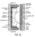
- Fig. 12shows, by way of example, a plasma display panel as an example of a device that incorporates barrier ribs that define the sub-pixels within the display.
- the barrier ribis an electrically insulating structure, and is preferably a high aspect ratio structure, as this improves the dot per inch resolution and fill factor of the display.
- What is neededis a system and method for efficiently producing closely spaced, high aspect-ratio gridlines that can be used, for example, in the production of high quality photovoltaic cells and plasma display panels.
- the present inventionis directed to an apparatus and a method for forming closely spaced high-aspect ratio gridline structures on a substrate surface in which the gridlines are co-extruded with a sacrificial material onto the substrate surface such that the high-aspect ratio gridline is supported between two sacrificial material portions (the sacrificial portions are subsequently removed).
- the formation of such co-extruded structuresrequires the compression of the gridline material between the two sacrificial material portions, which requires the use of a relatively wide three-channel cavity feeding a relatively narrow outlet orifice in a manner that compresses the gridline material between the two sacrificial material portions.
- the spacing between adjacent outlet orifices on each headis larger than the optimal gridline pitch used, for example, in solar cells.
- the relatively wide spacing between adjacent outlet orificesis compensated by disposing multiple co-extrusion heads in a parallel arrangement such that their respective outlet orifices are disposed in a staggered (offset) arrangement.
- the apparatus of claim 8further comprises an extrusion device coupled to a source of the sacrificial material and a source of the gridline material, wherein the first and second co-extrusion heads are fixedly mounted on the extrusion device.
- said means for movingcomprises means for fixedly securing the substrate, and means for moving the extrusion device over the surface of the substrate.
- said means for movingcomprises means for fixedly securing the extrusion device, and means for moving the substrate under the extrusion device.
- the apparatusfurther comprises at least one of means for heating the gridline and sacrificial materials before extrusion, means for cooling the substrate during extrusion of the gridline and sacrificial materials, and means for curing the extruded gridline and sacrificial materials.
- each of the first and second co-extrusion headscomprises a plurality of three-channel cavities, each of the three-channel cavities including a central channel and opposing first and second side channels, wherein the central channel and first and second side channels communicate with an associated outlet orifice, and wherein the means for causing the first and second co-extrusion heads to extrude gridline material and a sacrificial material includes means for injecting the gridline material into the central channel of each three-channel cavity while injecting the sacrificial material into the first and second side channels of said three-channel cavity.
- the three-channel cavityis defined between a first plate portion having a first inlet port disposed over the central channel of the three-channel cavity, and a second plate portion having second and third inlet ports respectively disposed over the first and second side channels of the three-channel cavity, and wherein said means for injecting the gridline material and the sacrificial material comprises means for forcing the gridline material through the first inlet port into the central channel while forcing the sacrificial material through the second and third inlet ports into the first and second side channels, respectively.
- a method for producing photovoltaic cellsincludes forming a suitable semiconductor substrate, and then forming closely spaced high aspect-ratio metal gridlines on a surface of the substrate in the manner described above.
- the methodfurther comprises at least one of cooling the substrate during extrusion of the materials, and curing the extruded materials.
- extruding the metal material and the sacrificial material through each of the first and second outlet orificescomprises injecting the metal material into a central channel of a three-channel cavity defined in one of said first and second co-extrusion heads while injecting the sacrificial material into opposing first and second side channels of the three-channel cavity, wherein the central channel and first and second side channels communicate with an associated outlet orifice.
- the three-channel cavityis defined between a first plate portion having a first inlet port disposed over the central channel of the three-channel cavity, and a second plate portion having second and third inlet ports respectively disposed over the first and second side channels of the three-channel cavity, and wherein extruding the metal material and the sacrificial material comprises forcing the metal material through the first inlet port into the central channel while forcing the sacrificial material through the second and third inlet ports into the first and second side channels, respectively.
- the methodfurther comprises:
- FIGURE 1is a perspective view showing an extrusion apparatus with an head for concurrently applying two or more materials on a substrate;
- FIGURE 2is an exploded perspective view showing a portion of a co-extrusion head utilized in the apparatus of FIGURE 1;
- FIGURE 3is an assembled perspective view showing the portion of the co-extrusion head of FIGURE 2 after manufacture
- FIGURES 4(A) and 4(B)are cross-sectional side views showing a three-channel cavity defined in the co-extrusion head of FIGURE 3;
- FIGURE 5is a cross-sectional side view showing an exemplary co-extruded gridline structure that was generated on a substrate surface by the co-extrusion head of FIGURE 4(B);
- FIGURE 6is a cross-sectional side view showing a larger portion of the co-extrusion head of FIGURE 4;
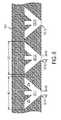
- FIGURE 7is a cross-sectional side view showing a series of co-extruded gridline structures generated by the co-extrusion head of FIGURE 6;
- FIGURE 8is an elevation view showing multiple co-extrusion heads in a staggered arrangement and closely spaced gridline structures generated by the multiple co-extrusion heads according to an aspect of the present invention
- FIGURE 9is a cross-sectional view showing a plurality of metal gridlines formed on a substrate according to another aspect of the present invention.
- FIGURE 10illustrates a photovoltaic cell including gridlines formed in accordance with the present invention
- FIGURE 11is a flow diagram showing a simplified method of forming a photovoltaic cell according to another embodiment of the present invention.
- FIGURE 12is a simplified cross-sectional side view showing a portion of an exemplary plasma display panel.
- FIGURE 1illustrates an extrusion apparatus 100 including an extrusion device 110 including two or more co-extrusion heads 130-1 and 130-2 fixedly mounted thereon.
- Extrusion device 110is coupled to a first source 111 containing a sacrificial material 112, and a second source 114 containing a gridline material 115.
- Extrusion heads 130-1 and 130-2are operably coupled to sources 111 and 114 such that heads 130-1 and 130-2 concurrently apply sacrificial material 112 and a gridline material 115 onto the upper surface 102 of a substrate 101.
- the materialsare applied through pushing and/or drawing techniques (e.g., hot and cold) in which the materials are pushed (e.g., squeezed, etc.) and/or drawn (e.g., via a vacuum, etc.) through extrusion device 110 and/or co-extrusion heads 130-1 and 130-2, and out one or more outlet orifices (exit ports) 135 that are respectively defined in a lower portion of co-extrusion heads 130-1 and 130-2.
- pushing and/or drawing techniquese.g., hot and cold
- extrusion device 110e.g., squeezed, etc.
- extrusion device 110e.g., via a vacuum, etc.
- co-extrusion heads 130-1 and 130-2are held by extrusion device 110 such that their respective outlet orifices are arranged in a parallel, spaced-apart arrangement.
- the (first) outlet orifices of co-extrusion head 130-1e.g., outlet orifices 135-11 and 135-12
- the (second) outlet orifices of the second co-extrusion head 130-2e.g., outlet orifices 135-21 and 135-22
- second line X2that is separated from and parallel to first line X1.
- apparatus 100includes a mechanism (not shown) for moving extrusion device 110 (and, hence, co-extrusion heads 130-1 and 130-2) in a direction that is perpendicular to the alignment direction of the outlet orifices.
- moving extrusion device 110 relative to substrate 101involves fixedly mounting substrate 101, and utilizing a positioning mechanism to move extrusion device 110 in a direction Y1 over surface 102 such that outlet orifices 135 are maintained at a fixed distance from surface 102.
- moving extrusion device 110 relative to substrate 101involves mounting device 110 to a rigid fixture, and utilizing a conveyor or other mechanism to move substrate 101 in a direction Y2 under outlet orifices 135.
- gridline material 112 and sacrificial material 115are co-extruded through outlet orifices 135 in a manner that creates parallel, elongated extruded structures 120 on substrate 101 such that the gridline material of each structure 120 forms a high-aspect ratio gridline structure 125, and the sacrificial material of each structure 120 forms associated first and second sacrificial material portions 122 respectively disposed on opposing sides of the associated high-aspect ratio gridline 125.
- extruded structures 120i.e., the aspect ratio of gridline 125 and the shape of sacrificial portions 122 are controllable through at least one of the shapes of the one or more outlet orifices 135, the structure within the heads 130-1 and 130-2 (e.g., channels), characteristics of the materials (e.g., viscosity, etc.), and the extrusion technique (e.g., flow rate, pressure, temperature, etc.).
- the structure within heads 130-1 and 130-2 and the shape of outlet orifices 135are described in additional detail below.
- Suitable gridline materials 115include, but are not limited to, silver, copper, nickel, tin, aluminum, steel, alumina, silicates, glasses, carbon black, polymers and waxes, and suitable sacrificial materials 112 include plastic, ceramic, oil, cellulose, latex, polymethylmethacrylate etc., combinations thereof, and/or variations thereof, including combining the above with other substances to obtain a desired density, viscosity, texture, color, etc.
- the (first) outlet orifices of co-extrusion head 130-1 and the (second) outlet orifices of co-extrusion head 130-2are disposed in a staggered arrangement such that extrusion structures 120 extruded by co-extrusion head 130-1 are disposed between two extrusion structures extruded by co-extrusion head 130-2.
- extrusion structure 120-12which is extruded from outlet orifice 135-12 of extrusion head 130-1, is disposed between extrusion structures 120-21 and 120-22, which are extruded from outlet orifices 135-21 and 135-22 of extrusion head 130-2.
- extruded structures 120 leaving extrusion heads 130-1 and 130-2can be quenched on substrate 101 by cooling the substrate using, for example, a quenching component 170.
- the ink used in this applicationmay be a hot-melt material, which solidifies at ambient temperatures, in which case the printheads 130-1 and 130-2 are heated, leaving the extruded structures 120 to solidify once they are dispensed onto the substrate 101.
- the materialscan be cured by thermal, optical and/or other means upon exit from extrusion heads 130-1 and 130-2.
- a curing component 180can be provided to thermally and/or optically cure the materials. If one or both materials include an ultraviolet curing agent, the material can be bound up into solid form in order to enable further processing without mixing.
- Figs. 2 and 3are exploded perspective and assembled perspective views showing an exemplary three-channel cavity 200-11 defined in co-extrusion head 130-1.
- three-channel cavity 200-11is utilized to produce extruded structure 120-11 by way of outlet orifice 135-11.
- Three-channel cavity 200-11is representative of the structural features employed in extrusion heads 130-1 and 130-2 to produce the multiple extrusion structures 120 shown in Fig. 1.
- co-extrusion head 130-1includes an upper sheet metal layer 210, a lower sheet metal layer 220, and a central sheet metal layer 230.
- Central metal layer 230is micro-machined (e.g., using deep reactive ion etching) to include an end structure 231 and an arrowhead-shaped opening including a central channel 232 and opposing (first and second) side channels 234 and 236.
- Central channel 232is separated from side channel 234 by a first tapered finger 233, and is separated from side channel 236 by a second tapered finger 235.
- Central channel 232has a closed end that is defined by end structure 231 and tapered fingers 233 and 235, and an open end that communicates with an opening 237 defined in a side edge 238 of plate 230.
- side channels 234 and 236have associated closed ends that are defined by end structure 231 and tapered fingers 233 and 235, and open ends that communicate with opening 237.
- Side channels 234 and 236are angled toward central channel 232, and converge adjacent opening 237.
- Upper metal plate 210defines a first inlet port (through hole) 212
- lower metal plate 220defines second and third inlet ports 224 and 226. Inlet ports 212, 224 and 226 are formed, for example, using the same micro-machining techniques used to form three-channel cavity 231-11.
- Fig. 3shows the portion of head 130-1 of Fig. 2 after plates 210, 220 and 230 are bonded using known high pressure wafer bonding techniques to define three-channeled cavity 200-11.
- First inlet port 212is aligned with the closed end of central channel 232
- second and third inlet ports 224 and 226are aligned with the closed ends of side channels 234 and 236, respectively.
- metal and sacrificial materialsare introduced into three-channel cavity 231 through inlet ports 212, 224 and 226. Additional metal plates (not shown) may be utilized to conduct the metal and sacrificial materials to the inlet ports 212, 224 and 226 in a manner that minimizes the number of material feedlines attached to each extrusion head.
- extrusion head 130-1can be manufactured a variety of ways.
- the extrusion headscan be manufactured by electroplating metal up through features in a patterned resist structure.
- the headscan be manufactured by brazing together layers of etched sheet metal.
- the headscan be manufactured by generating structures out of photo-definable polymer such as SU8.
- the headscan be machined or molded out of metal and/or plastic using conventional manufacturing techniques.
- extrusion heads 130-1 and 130-2may be modified to produce gridline structures having an equilibrium shape, as described in co-owned and co-pending U.S.
- Fig. 4(A)shows a portion of co-extrusion head 130-1 positioned over substrate 101 prior to generation of metal gridlines.
- Co-extrusion head 130-1is maintained at a substantially fixed distance D over upper surface 102 of substrate 101 during the extrusion process (i.e., while co-extrusion head 130-1 is moved relative to substrate 101 in the manner described above).
- the distance D between the head 130-11 and the substrate 101can be based on various factors, such as the angle of the dispensing end of the head 130-11 with respect to upper surface 102 (e.g., from parallel to perpendicular), in order to increase transfer efficiency, entity definition (e.g., width, height, length, diameter, etc), entity characteristics (e.g., strength, pliability, etc.), etc.
- distance Dmust be greater than or equal to the height H (shown in Fig. 5) of extruded structure 120-11 in order to facilitate the staggered extrusion head arrangement shown in Fig. 1.
- Fig. 4(B)shows the same portion of co-extrusion head 130-1 at the onset of the co-extrusion process.
- gridline material 112is forcibly injected through the first inlet port 212 into the closed end of central channel 232, and sacrificial material 115 is simultaneously forcibly injected through inlet ports 224 and 226 into side channels 234 and 236, respectively.
- the injected materialstravel downward along their respective channels.
- the gridline and sacrificial materialsare compressed by the tapered shapes channels 232, 234 and 236.
- the gridline materialis further compressed by the converging sacrificial material flowing along side channels 234 and 236 as the materials approach outlet orifice 135-11.
- the compressed flowis then extruded from outlet orifice 135-11 and is deposited on substrate 101 as extruded structure 120-11 (shown in Fig. 5). Intermixing between the gridline and sacrificial materials is minimized by choosing appropriate materials and viscosities, by appropriately tapering the channels, and/or by maintaining laminar flow conditions.
- Fig. 5is a cross-sectional side view showing an exemplary extruded structure 120-11 produced in accordance with the co-extrusion process described with reference to Fig. 4(B).
- Extruded structure 120-11includes a gridline 125-11 disposed between sacrificial support material portions 122-1 and 122-2. Due to the converging forces generated by three-channel cavity 200-11 (Figs. 4(A) and 4(B)) leading to outlet 135-11, extruded structure 120-11 exhibits advantages over gridlines formed by conventional methods.
- extrusion head 130-1facilitates the formation of gridline 125-11 with an aspect ratio (height H to width W) of 10:1 or greater in a single pass, which is not possible using conventional methods.
- the width W of gridline 125-11can be made narrower (finer) than the smallest minimum design feature of extruder head 130-11.
- Sacrificial material portions 122-1 and 122-2are maintained along the sides of gridline 125-11 only as long as it is needed to maintain the shape of gridline 125-11 on substrate 101 before or during subsequent processing such as drying, curing, and/or sintering.
- a further advantage of sacrificial material portions 122-1 and 122-2is that the added material leads to an overall larger outlet orifice, and hence a lower pressure drop for a given material flow speed. Higher process speed is therefore achievable.
- the compressing flowcan be manipulated to form metal gridline 125-11 with a tapered cross-section (e.g., with a relatively wide base disposed on substrate surface 102, a relatively narrow upper end, and tapered sides that extend at an angle relative to surface 102 from the base end to the upper end).
- This tapered shapefacilitates directing photons into substrate 101, and reduces the photon blocking (shading) caused by the gridlines, which can improve efficiency and/or generation of electrical power.
- FIGURE 6is a cross-sectional view showing a larger portion of extrusion head 130-1
- FIGURE 7depicts a series of extrusion structures 120-11, 120-12 and 120-13 that are produced extrusion head 130-1 in the manner described above.
- a spacing P between adjacent extrusion structures 120-11 to 120-13 extruded from a single co-extrusion headis limited by the spacing between the adjacent outlet orifices, which in turn is limited by the upstream space needed to form the three channels of each three-channel cavity.
- This wide upstream spaceis shown in Fig. 6, where extrusion head 130-1 includes adjacent three-channel cavities 200-11, 200-12, and 200-13 that respectively define outlet orifices 135-11, 135-12 and 135-13.
- the inlet ports associated with channel cavities 200-11, 200-12, and 200-13are omitted for clarity. As indicated in Fig.
- FIGURE 8is a side view depicting co-extrusion heads 130-1 and 130-2 in a staggered arrangement that facilitates the production of closely spaced gridlines structures on substrate 101 according to an embodiment of the present invention.
- co-extrusion heads 130-1 and 130-2are fixedly held over substrate 101 in a parallel arrangement, with their respective outlet orifices aligned in a staggered arrangement such that at least one extrusion structure extruded from co-extrusion head 130-1 is disposed between two extrusion structures extruded from co-extrusion head 130-2.
- outlet orifice 135-12 of co-extrusion head 130-1produces extrusion structure 120-12, which is disposed between extrusion structures 120-21 and 120-22, which are extruded by outlet orifices 135-21 and 135-22, respectively, of co-extrusion head 130-2.
- a distance between adjacent extrusion structuresis reduced to P/2, as indicated at the bottom of Fig. 8.
- co-extrusion heads 130-1 and 130-2in a staggered arrangement, extrusion structures produced by the extrusion apparatus 100 of Fig. 1 have a finer pitch and higher aspect-ratio that those produced using conventional methods, thereby facilitating the production of, for example, superior photovoltaic cells.
- FIGURE 9is a cross-sectional side view depicting the removal of sacrificial material using a suitable etchant (indicated by slanted lines), thereby completing the process of forming closely spaced, high aspect-ratio gridlines 125-11, 125-21, 125-12, 125-22, and 125-13 on upper surface 102.
- the preferred means to remove the sacrificial materialis through evaporation and combustion during the firing process.
- This processalso consolidates the metal particles in the gridline material (metal paste consisting of silver particles, a glass frit, a solvent such as terpineol, and fillers such as cellulose) into a conducting mass.
- the firing stepalso causes the metal paste to fire through the insulating passivation layer on the surface of the solar cell, often aided by glass frit particles in the paste, in order to make electrical contact to the semiconductor layer.
- FIGURE 10illustrates an exemplary portion of a photovoltaic cell 300, such as a solar cell, with high-aspect metal gridlines 125 created via co-extrusion heads 130-1 and 130-2.
- Photovoltaic cell 300includes a semiconductor substrate 301 with a p-type region 306 and an n-type region 308.
- One or both of the regions 306 and 308 of substrate 301is formed from semiconductor materials such as, for example, Aluminium Arsenide, Aluminium Gallium Arsenide, Boron Nitride, Cadmium Sulfide, Cadmium Selenide, Copper Indium Gallium Selenide, Diamond, Gallium Arsenide, Gallium Nitride, Germanium, Indium Phosphide, Silicon, Silicon Carbide, Silicon Germanium, Silicon on insulator, Zinc Sulfide, Zinc Selenide, etc.
- a lower contact 310is formed on a lower surface 302 of substrate 301 (i.e., at a lower end of p-type region 306).
- Metal gridlines 125 and one or more bus bars 320are formed on an upper surface 304 of substrate 301 (i.e., at a lower end of n-type region 308).
- Contact 310 and bus bars 320can be formed using a metal paste such as a silver or an aluminum based paste.
- Photovoltaic cell 300can be interconnected with other photovoltaic cells (not shown) in series and/or parallel, for example, via flat wires or metal ribbons, and assembled into modules or panels and connected as indicated to a load 340.
- a sheet of tempered glass(not shown) may be layered over the gridlines 125 and/or a polymer encapsulation (not shown) may be formed over the contact 310.
- Upper surface 304may include a textured surface and/or be coated with an antireflection material (e.g., silicon nitride, titanium dioxide, etc.) in order to increase the amount of light absorbed into the cell.
- an antireflection materiale.g., silicon nitride, titanium dioxide, etc.
- FIGURE 11illustrates a method for fabricating a photovoltaic device such as photovoltaic cell 300 described in connection with FIGURE 10.
- semiconductor substrate 301(Fig. 10) is formed.
- Substrate 301can include various semiconductor materials as described above, and may be formed by coupling a piece of n-type silicon with a piece of p-type silicon, or by diffusing an n-type dopant (e.g., Phosphorus, Arsenic, Antimony, etc.) and/or a p-type dopant (e.g., Boron, etc.) is diffused into a silicon wafer.
- an n-type dopante.g., Phosphorus, Arsenic, Antimony, etc.
- a p-type dopante.g., Boron, etc.
- naturally occurring semiconductorssuch as blue diamonds, which contain Boron impurities, can be used.
- One or more of the photovoltaic cellscan optionally be coupled in a serial and/or parallel manner to create a photovoltaic module or panel.
- conducting contactis formed on lower surface 302 using known techniques.
- a metal gridlines 125(and bus bars 320) are formed on upper surface 304 using the methods described above.
- electrodesare coupled from conducting contact 310 and gridlines 125 to load 340 in the manner shown in Fig. 10. When photons are absorbed into the semiconductor, electrical energy is generated via the photovoltaic effect.
- a co-extrusion headwith the estimated parameters illustrated in Table 1 could be used to dispense the materials to make gridlines 125 on a crystalline silicon solar cell.
- Table 1Exemplary head parameters for generating a gridline. Sheet Thickness 152 microns Gridline Pitch 2.5 mm Head Speed 1 cm/sec Past Viscosity 100,000 Cp Head Angle 45 degrees Head Exit Width 304.8 Microns Silver Width 49.2 microns Silver Line Cross Section 7,500 microns ⁇ 2 Silver Line Aspect Ratio 3.10:1 Silver Flow 0.075 mm ⁇ 3/sec Head Compression 6.2:1 Head Pressure Drop 2.24 atm
- convergent channelsare patterned into a sheet of material with a thickness of approximately 0.15 mm.
- the outlet orifices of the head/nozzlesare repeated on a pitch of 2.5 mm.
- paste of 1000 poiseis ejected at a rate of 1 cm/sec.
- the central stripe of silveris approximately 50 microns wide with an aspect ratio of 3:1.
- variations of heads 130-1 and 130-2may be used to additionally and/or alternatively introduce materials with a vertical variation, for example, for introducing barrier layers onto the substrate.
- Such vertical variationcan be implemented by forming channels that converge dissimilar materials together in the vertical direction (in addition to converging in the horizontal direction) within the manifold.
- a metal bi-layeronto the cell surface with one metal making contact to the silicon as a diffusion barrier, and a second metal on top selected for either lower cost or higher conductance.
- the methods and structures described hereinmay be utilized to generate gridlines formed from electrically non-conductive materials, such as inorganic glasses that are used, for example, to produce the barrier rib structures described with reference to Fig. 12.
Landscapes
- Engineering & Computer Science (AREA)
- Mechanical Engineering (AREA)
- Chemical & Material Sciences (AREA)
- Chemical Kinetics & Catalysis (AREA)
- Electrochemistry (AREA)
- General Chemical & Material Sciences (AREA)
- Physics & Mathematics (AREA)
- Plasma & Fusion (AREA)
- Manufacturing & Machinery (AREA)
- Extrusion Moulding Of Plastics Or The Like (AREA)
- Photovoltaic Devices (AREA)
- Application Of Or Painting With Fluid Materials (AREA)
Abstract
Description
- The present invention is related to extrusion systems and methods, and more particularly to micro extrusion systems and methods for co-extruding multiple similar and/or dissimilar materials to form relatively fine structures with relatively high aspect ratios.
- With traditional extrusion a billet of material is pushed and/or drawn through a die to create a rod, rail, pipe, etc. Various applications leverage this capability. For instance, extrusion can be used with food processing applications to create pasta, cereal, snacks, etc., pipe pastry filling (e.g., meringue), pattern cookie dough on a cookie pan, generate pastry flowers and borders on cakes, etc. In another application, extrusion can be used with consumer goods, for example, to merge different colored toothpastes together on a toothbrush.
- Conventional extrusion techniques are limited, for example, in that they cannot render relatively high aspect-ratio (e.g., 2:1 or greater) fine featured (e.g., less than 50 micron) or porous structures. Thus, extrusion typically is not used for creating conducting contacts and/or channels for electrochemical (e.g., fuel), solar, and/or other types of cells, which leverage high aspect-ratio fine featured porous structures to increase efficiency and electrical power generation.
- By way of example, with fuel cells, high aspect-ratio fine featured porous electrolyte structures provide a long reaction zone that increases utilization of the expensive catalyst needed for the electrode. In addition, fuel cells can be complex structures since they perform multiple functions including: conducting protons from the membrane to the reaction site; diffusing oxygen to the reaction site with a low partial pressure drop; conducting electrons from the porous electrode to the reaction site; carrying heat away from the reaction site; and withstanding a compressive mechanical load in a range of about 100 to 200 PSI. Conventional extrusion techniques cannot meet these demands at a cost demanded by the fuel cell industry. In order to increase efficiency, fuel cell manufacturers use more catalyst than desired to increase the number of reaction sites and make agglomerates of carbon catalyzed with Platinum (Pt) in a matrix of porous, or polytetrafluoroethylene (PTFE). With solar cells, high aspect-ratio fine featured grid lines reduce the amount of shading, which allows more photons to be captured, resulting in an increased electrical power generation. Conventional extrusion techniques are not able to produce such gridlines at a cost demanded by the solar cell industry.
- There are many other practical devices that benefit from rapid and economical means for generating high aspect ratio lines and features. Fig. 12 shows, by way of example, a plasma display panel as an example of a device that incorporates barrier ribs that define the sub-pixels within the display. The barrier rib is an electrically insulating structure, and is preferably a high aspect ratio structure, as this improves the dot per inch resolution and fill factor of the display.
- What is needed is a system and method for efficiently producing closely spaced, high aspect-ratio gridlines that can be used, for example, in the production of high quality photovoltaic cells and plasma display panels.
- The present invention is directed to an apparatus and a method for forming closely spaced high-aspect ratio gridline structures on a substrate surface in which the gridlines are co-extruded with a sacrificial material onto the substrate surface such that the high-aspect ratio gridline is supported between two sacrificial material portions (the sacrificial portions are subsequently removed). The formation of such co-extruded structures requires the compression of the gridline material between the two sacrificial material portions, which requires the use of a relatively wide three-channel cavity feeding a relatively narrow outlet orifice in a manner that compresses the gridline material between the two sacrificial material portions. Due to the width of the three-channel cavity, the spacing between adjacent outlet orifices on each head (and, hence, the pitch of the extruded gridlines) is larger than the optimal gridline pitch used, for example, in solar cells. According to the present invention, the relatively wide spacing between adjacent outlet orifices is compensated by disposing multiple co-extrusion heads in a parallel arrangement such that their respective outlet orifices are disposed in a staggered (offset) arrangement. When the assembly is subsequently moved over the substrate and co-extruded materials are forced from the respective outlet orifices, the interspersed parallel gridlines are produced that have a desired (relatively small) pitch. When the sacrificial material is subsequently removed, the resulting closely-spaced, high aspect ratio gridlines are provided on the substrate surface.
In one embodiment the apparatus of claim 8, further comprises an extrusion device coupled to a source of the sacrificial material and a source of the gridline material, wherein the first and second co-extrusion heads are fixedly mounted on the extrusion device.
In a further embodiment said means for moving comprises means for fixedly securing the substrate, and means for moving the extrusion device over the surface of the substrate.
In a further embodiment said means for moving comprises means for fixedly securing the extrusion device, and means for moving the substrate under the extrusion device.
In a further embodiment the apparatus further comprises at least one of means for heating the gridline and sacrificial materials before extrusion, means for cooling the substrate during extrusion of the gridline and sacrificial materials, and means for curing the extruded gridline and sacrificial materials.
In a further embodiment each of the first and second co-extrusion heads comprises a plurality of three-channel cavities, each of the three-channel cavities including a central channel and opposing first and second side channels, wherein the central channel and first and second side channels communicate with an associated outlet orifice,
and wherein the means for causing the first and second co-extrusion heads to extrude gridline material and a sacrificial material includes means for injecting the gridline material into the central channel of each three-channel cavity while injecting the sacrificial material into the first and second side channels of said three-channel cavity.
In a further embodiment the three-channel cavity is defined between a first plate portion having a first inlet port disposed over the central channel of the three-channel cavity, and a second plate portion having second and third inlet ports respectively disposed over the first and second side channels of the three-channel cavity, and
wherein said means for injecting the gridline material and the sacrificial material comprises means for forcing the gridline material through the first inlet port into the central channel while forcing the sacrificial material through the second and third inlet ports into the first and second side channels, respectively. - In accordance with a specific embodiment of the present invention, a method for producing photovoltaic cells includes forming a suitable semiconductor substrate, and then forming closely spaced high aspect-ratio metal gridlines on a surface of the substrate in the manner described above.
In a further embodiment the method further comprises at least one of cooling the substrate during extrusion of the materials, and curing the extruded materials.
In a further embodiment extruding the metal material and the sacrificial material through each of the first and second outlet orifices comprises injecting the metal material into a central channel of a three-channel cavity defined in one of said first and second co-extrusion heads while injecting the sacrificial material into opposing first and second side channels of the three-channel cavity, wherein the central channel and first and second side channels communicate with an associated outlet orifice.
In a further embodiment the three-channel cavity is defined between a first plate portion having a first inlet port disposed over the central channel of the three-channel cavity, and a second plate portion having second and third inlet ports respectively disposed over the first and second side channels of the three-channel cavity, and
wherein extruding the metal material and the sacrificial material comprises forcing the metal material through the first inlet port into the central channel while forcing the sacrificial material through the second and third inlet ports into the first and second side channels, respectively.
In a further embodiment the method further comprises: - forming a conductive contact layer on the first surface of the semiconductor substrate; and
- connecting a first electrode to the metal gridlines, and a second electrode to the conductive contact layer.
- These and other features, aspects and advantages of the present invention will become better understood with regard to the following description, appended claims, and accompanying drawings, where:
- FIGURE 1 is a perspective view showing an extrusion apparatus with an head for concurrently applying two or more materials on a substrate;
- FIGURE 2 is an exploded perspective view showing a portion of a co-extrusion head utilized in the apparatus of FIGURE 1;
- FIGURE 3 is an assembled perspective view showing the portion of the co-extrusion head of FIGURE 2 after manufacture;
- FIGURES 4(A) and 4(B) are cross-sectional side views showing a three-channel cavity defined in the co-extrusion head of FIGURE 3;
- FIGURE 5 is a cross-sectional side view showing an exemplary co-extruded gridline structure that was generated on a substrate surface by the co-extrusion head of FIGURE 4(B);
- FIGURE 6 is a cross-sectional side view showing a larger portion of the co-extrusion head of FIGURE 4;
- FIGURE 7 is a cross-sectional side view showing a series of co-extruded gridline structures generated by the co-extrusion head of FIGURE 6;
- FIGURE 8 is an elevation view showing multiple co-extrusion heads in a staggered arrangement and closely spaced gridline structures generated by the multiple co-extrusion heads according to an aspect of the present invention;
- FIGURE 9 is a cross-sectional view showing a plurality of metal gridlines formed on a substrate according to another aspect of the present invention;
- FIGURE 10 illustrates a photovoltaic cell including gridlines formed in accordance with the present invention;
- FIGURE 11 is a flow diagram showing a simplified method of forming a photovoltaic cell according to another embodiment of the present invention; and
- FIGURE 12 is a simplified cross-sectional side view showing a portion of an exemplary plasma display panel.
- FIGURE 1 illustrates an
extrusion apparatus 100 including anextrusion device 110 including two or more co-extrusion heads 130-1 and 130-2 fixedly mounted thereon.Extrusion device 110 is coupled to afirst source 111 containing asacrificial material 112, and asecond source 114 containing agridline material 115. Extrusion heads 130-1 and 130-2 are operably coupled tosources sacrificial material 112 and agridline material 115 onto theupper surface 102 of asubstrate 101. The materials are applied through pushing and/or drawing techniques (e.g., hot and cold) in which the materials are pushed (e.g., squeezed, etc.) and/or drawn (e.g., via a vacuum, etc.) throughextrusion device 110 and/or co-extrusion heads 130-1 and 130-2, and out one or more outlet orifices (exit ports) 135 that are respectively defined in a lower portion of co-extrusion heads 130-1 and 130-2. - In accordance with an aspect of the invention, co-extrusion heads 130-1 and 130-2 are held by
extrusion device 110 such that their respective outlet orifices are arranged in a parallel, spaced-apart arrangement. In particular, the (first) outlet orifices of co-extrusion head 130-1 (e.g., outlet orifices 135-11 and 135-12) extending in a first direction X1, and the (second) outlet orifices of the second co-extrusion head 130-2 (e.g., outlet orifices 135-21 and 135-22) define a second line X2 that is separated from and parallel to first line X1. - In accordance with another aspect of the present invention,
apparatus 100 includes a mechanism (not shown) for moving extrusion device 110 (and, hence, co-extrusion heads 130-1 and 130-2) in a direction that is perpendicular to the alignment direction of the outlet orifices. In one embodiment, movingextrusion device 110 relative tosubstrate 101 involves fixedly mountingsubstrate 101, and utilizing a positioning mechanism to moveextrusion device 110 in a direction Y1 oversurface 102 such thatoutlet orifices 135 are maintained at a fixed distance fromsurface 102. In an alternative embodiment, movingextrusion device 110 relative tosubstrate 101 involves mountingdevice 110 to a rigid fixture, and utilizing a conveyor or other mechanism to movesubstrate 101 in a direction Y2 under outlet orifices 135. - In accordance with another aspect of the present invention, while
extrusion device 110 is being moved relative tosubstrate 101,gridline material 112 andsacrificial material 115 are co-extruded throughoutlet orifices 135 in a manner that creates parallel, elongatedextruded structures 120 onsubstrate 101 such that the gridline material of eachstructure 120 forms a high-aspectratio gridline structure 125, and the sacrificial material of eachstructure 120 forms associated first and secondsacrificial material portions 122 respectively disposed on opposing sides of the associated high-aspect ratio gridline 125. The shape of extruded structures 120 (i.e., the aspect ratio ofgridline 125 and the shape of sacrificial portions 122) are controllable through at least one of the shapes of the one ormore outlet orifices 135, the structure within the heads 130-1 and 130-2 (e.g., channels), characteristics of the materials (e.g., viscosity, etc.), and the extrusion technique (e.g., flow rate, pressure, temperature, etc.). The structure within heads 130-1 and 130-2 and the shape ofoutlet orifices 135 are described in additional detail below.Suitable gridline materials 115 include, but are not limited to, silver, copper, nickel, tin, aluminum, steel, alumina, silicates, glasses, carbon black, polymers and waxes, and suitablesacrificial materials 112 include plastic, ceramic, oil, cellulose, latex, polymethylmethacrylate etc., combinations thereof, and/or variations thereof, including combining the above with other substances to obtain a desired density, viscosity, texture, color, etc. - In accordance with another aspect of the present invention, the (first) outlet orifices of co-extrusion head 130-1 and the (second) outlet orifices of co-extrusion head 130-2 are disposed in a staggered arrangement such that
extrusion structures 120 extruded by co-extrusion head 130-1 are disposed between two extrusion structures extruded by co-extrusion head 130-2. For example, extrusion structure 120-12, which is extruded from outlet orifice 135-12 of extrusion head 130-1, is disposed between extrusion structures 120-21 and 120-22, which are extruded from outlet orifices 135-21 and 135-22 of extrusion head 130-2. As described in additional detail below, by utilizing two or more parallel extrusion heads (e.g., heads 130-1 and 130-2) to simultaneously generateextrusion structures 120, closely spaced high aspect-ratio gridlines 125 are formed onsubstrate 101 at a pitch that is not possible using conventional methods. - Referring again to Fig. 1, to limit the tendency for the materials to intermix after extrusion, extruded
structures 120 leaving extrusion heads 130-1 and 130-2 can be quenched onsubstrate 101 by cooling the substrate using, for example, aquenching component 170. Alternately, the ink used in this application may be a hot-melt material, which solidifies at ambient temperatures, in which case the printheads 130-1 and 130-2 are heated, leaving theextruded structures 120 to solidify once they are dispensed onto thesubstrate 101. In another technique, the materials can be cured by thermal, optical and/or other means upon exit from extrusion heads 130-1 and 130-2. For example, acuring component 180 can be provided to thermally and/or optically cure the materials. If one or both materials include an ultraviolet curing agent, the material can be bound up into solid form in order to enable further processing without mixing. - Figs. 2 and 3 are exploded perspective and assembled perspective views showing an exemplary three-channel cavity 200-11 defined in co-extrusion head 130-1. Referring briefly to Fig. 1, three-channel cavity 200-11 is utilized to produce extruded structure 120-11 by way of outlet orifice 135-11. Three-channel cavity 200-11 is representative of the structural features employed in extrusion heads 130-1 and 130-2 to produce the
multiple extrusion structures 120 shown in Fig. 1. - Referring to Fig. 2, in accordance with an embodiment of the present invention, co-extrusion head 130-1 includes an upper
sheet metal layer 210, a lowersheet metal layer 220, and a centralsheet metal layer 230.Central metal layer 230 is micro-machined (e.g., using deep reactive ion etching) to include anend structure 231 and an arrowhead-shaped opening including acentral channel 232 and opposing (first and second)side channels Central channel 232 is separated fromside channel 234 by a firsttapered finger 233, and is separated fromside channel 236 by a secondtapered finger 235.Central channel 232 has a closed end that is defined byend structure 231 and taperedfingers opening 237 defined in aside edge 238 ofplate 230. Similarly,side channels end structure 231 and taperedfingers opening 237.Side channels central channel 232, and convergeadjacent opening 237.Upper metal plate 210 defines a first inlet port (through hole) 212, andlower metal plate 220 defines second andthird inlet ports Inlet ports - Fig. 3 shows the portion of head 130-1 of Fig. 2 after
plates First inlet port 212 is aligned with the closed end ofcentral channel 232, and second andthird inlet ports side channels channel cavity 231 throughinlet ports inlet ports - In addition to the laminated metal layer arrangement depicted in Figs. 2 and 3, extrusion head 130-1 can be manufactured a variety of ways. In another embodiment, the extrusion heads can be manufactured by electroplating metal up through features in a patterned resist structure. In another instance, the heads can be manufactured by brazing together layers of etched sheet metal. In yet another instance, the heads can be manufactured by generating structures out of photo-definable polymer such as SU8. In still another instance, the heads can be machined or molded out of metal and/or plastic using conventional manufacturing techniques. Moreover, in addition to the specific gridline structures described herein, extrusion heads 130-1 and 130-2 may be modified to produce gridline structures having an equilibrium shape, as described in co-owned and co-pending U.S. Patent Application Serial No. xx/xxx,xxx, entitled "EXTRUDED STRUCTURE WITH EQUILIBRIUM SHAPE" [Atty Docket No. 20060464-US-NP (XCP-073)], which is incorporated herein by reference in its entirety.
- Fig. 4(A) shows a portion of co-extrusion head 130-1 positioned over
substrate 101 prior to generation of metal gridlines. Co-extrusion head 130-1 is maintained at a substantially fixed distance D overupper surface 102 ofsubstrate 101 during the extrusion process (i.e., while co-extrusion head 130-1 is moved relative tosubstrate 101 in the manner described above). The distance D between the head 130-11 and thesubstrate 101 can be based on various factors, such as the angle of the dispensing end of the head 130-11 with respect to upper surface 102 (e.g., from parallel to perpendicular), in order to increase transfer efficiency, entity definition (e.g., width, height, length, diameter, etc), entity characteristics (e.g., strength, pliability, etc.), etc. Note that distance D must be greater than or equal to the height H (shown in Fig. 5) of extruded structure 120-11 in order to facilitate the staggered extrusion head arrangement shown in Fig. 1. - Fig. 4(B) shows the same portion of co-extrusion head 130-1 at the onset of the co-extrusion process. As indicated by the white arrows,
gridline material 112 is forcibly injected through thefirst inlet port 212 into the closed end ofcentral channel 232, andsacrificial material 115 is simultaneously forcibly injected throughinlet ports side channels shapes channels side channels substrate 101 as extruded structure 120-11 (shown in Fig. 5). Intermixing between the gridline and sacrificial materials is minimized by choosing appropriate materials and viscosities, by appropriately tapering the channels, and/or by maintaining laminar flow conditions. - Fig. 5 is a cross-sectional side view showing an exemplary extruded structure 120-11 produced in accordance with the co-extrusion process described with reference to Fig. 4(B). Extruded structure 120-11 includes a gridline 125-11 disposed between sacrificial support material portions 122-1 and 122-2. Due to the converging forces generated by three-channel cavity 200-11 (Figs. 4(A) and 4(B)) leading to outlet 135-11, extruded structure 120-11 exhibits advantages over gridlines formed by conventional methods. For example, extrusion head 130-1 facilitates the formation of gridline 125-11 with an aspect ratio (height H to width W) of 10:1 or greater in a single pass, which is not possible using conventional methods. The width W of gridline 125-11 can be made narrower (finer) than the smallest minimum design feature of extruder head 130-11. Sacrificial material portions 122-1 and 122-2 are maintained along the sides of gridline 125-11 only as long as it is needed to maintain the shape of gridline 125-11 on
substrate 101 before or during subsequent processing such as drying, curing, and/or sintering. A further advantage of sacrificial material portions 122-1 and 122-2 is that the added material leads to an overall larger outlet orifice, and hence a lower pressure drop for a given material flow speed. Higher process speed is therefore achievable. In addition, the compressing flow can be manipulated to form metal gridline 125-11 with a tapered cross-section (e.g., with a relatively wide base disposed onsubstrate surface 102, a relatively narrow upper end, and tapered sides that extend at an angle relative to surface 102 from the base end to the upper end). This tapered shape facilitates directing photons intosubstrate 101, and reduces the photon blocking (shading) caused by the gridlines, which can improve efficiency and/or generation of electrical power. - FIGURE 6 is a cross-sectional view showing a larger portion of extrusion head 130-1, and FIGURE 7 depicts a series of extrusion structures 120-11, 120-12 and 120-13 that are produced extrusion head 130-1 in the manner described above.
- Referring to Fig. 7, a spacing P between adjacent extrusion structures 120-11 to 120-13 extruded from a single co-extrusion head (e.g., head 130-1) is limited by the spacing between the adjacent outlet orifices, which in turn is limited by the upstream space needed to form the three channels of each three-channel cavity. This wide upstream space is shown in Fig. 6, where extrusion head 130-1 includes adjacent three-channel cavities 200-11, 200-12, and 200-13 that respectively define outlet orifices 135-11, 135-12 and 135-13. The inlet ports associated with channel cavities 200-11, 200-12, and 200-13 are omitted for clarity. As indicated in Fig. 6, in contrast to the relatively narrow width W1 of outlet orifice 135-11, a relatively large width W2 is needed to define
channels co-extrusion structures 120 using a single co-extrusion head). - FIGURE 8 is a side view depicting co-extrusion heads 130-1 and 130-2 in a staggered arrangement that facilitates the production of closely spaced gridlines structures on
substrate 101 according to an embodiment of the present invention. In particular, in a manner consistent with that shown in Fig. 1, co-extrusion heads 130-1 and 130-2 are fixedly held oversubstrate 101 in a parallel arrangement, with their respective outlet orifices aligned in a staggered arrangement such that at least one extrusion structure extruded from co-extrusion head 130-1 is disposed between two extrusion structures extruded from co-extrusion head 130-2. By way of example, as indicated in Fig. 8, outlet orifice 135-12 of co-extrusion head 130-1 produces extrusion structure 120-12, which is disposed between extrusion structures 120-21 and 120-22, which are extruded by outlet orifices 135-21 and 135-22, respectively, of co-extrusion head 130-2. In this manner, a distance between adjacent extrusion structures (and, hence, their associated gridlines) is reduced to P/2, as indicated at the bottom of Fig. 8. Thus, by arranging co-extrusion heads 130-1 and 130-2 in a staggered arrangement, extrusion structures produced by theextrusion apparatus 100 of Fig. 1 have a finer pitch and higher aspect-ratio that those produced using conventional methods, thereby facilitating the production of, for example, superior photovoltaic cells. - FIGURE 9 is a cross-sectional side view depicting the removal of sacrificial material using a suitable etchant (indicated by slanted lines), thereby completing the process of forming closely spaced, high aspect-ratio gridlines 125-11, 125-21, 125-12, 125-22, and 125-13 on
upper surface 102. - In some applications, including the manufacture of solar cell gridlines, the preferred means to remove the sacrificial material is through evaporation and combustion during the firing process. This process also consolidates the metal particles in the gridline material (metal paste consisting of silver particles, a glass frit, a solvent such as terpineol, and fillers such as cellulose) into a conducting mass. In one embodiment, the firing step also causes the metal paste to fire through the insulating passivation layer on the surface of the solar cell, often aided by glass frit particles in the paste, in order to make electrical contact to the semiconductor layer.
- FIGURE 10 illustrates an exemplary portion of a
photovoltaic cell 300, such as a solar cell, with high-aspect metal gridlines 125 created via co-extrusion heads 130-1 and 130-2.Photovoltaic cell 300 includes asemiconductor substrate 301 with a p-type region 306 and an n-type region 308. One or both of theregions substrate 301 is formed from semiconductor materials such as, for example, Aluminium Arsenide, Aluminium Gallium Arsenide, Boron Nitride, Cadmium Sulfide, Cadmium Selenide, Copper Indium Gallium Selenide, Diamond, Gallium Arsenide, Gallium Nitride, Germanium, Indium Phosphide, Silicon, Silicon Carbide, Silicon Germanium, Silicon on insulator, Zinc Sulfide, Zinc Selenide, etc. Alower contact 310 is formed on alower surface 302 of substrate 301 (i.e., at a lower end of p-type region 306).Metal gridlines 125 and one ormore bus bars 320 are formed on anupper surface 304 of substrate 301 (i.e., at a lower end of n-type region 308). Contact 310 andbus bars 320 can be formed using a metal paste such as a silver or an aluminum based paste. Photovoltaic cell 300 can be interconnected with other photovoltaic cells (not shown) in series and/or parallel, for example, via flat wires or metal ribbons, and assembled into modules or panels and connected as indicated to aload 340. A sheet of tempered glass (not shown) may be layered over thegridlines 125 and/or a polymer encapsulation (not shown) may be formed over thecontact 310.Upper surface 304 may include a textured surface and/or be coated with an antireflection material (e.g., silicon nitride, titanium dioxide, etc.) in order to increase the amount of light absorbed into the cell.- During operation, when photons 350 (indicated by wide arrows) are directed into
substrate 301 throughupper surface 304, their energy excites electron-hole pairs therein, which subsequently freely move. In particular, absorption of a photon creates an electric current through the p-n junction (depicted by the migrating + and - charges). Electrical current is generated when excited electrons in the n-type region 308 travel throughgridlines 125,bus bar 320, and the electrodes toexternal load 340 and back through the lower electrode and contact 310 to the p-type region 306. - FIGURE 11 illustrates a method for fabricating a photovoltaic device such as
photovoltaic cell 300 described in connection with FIGURE 10. Atreference numeral 410, semiconductor substrate 301 (Fig. 10) is formed.Substrate 301 can include various semiconductor materials as described above, and may be formed by coupling a piece of n-type silicon with a piece of p-type silicon, or by diffusing an n-type dopant (e.g., Phosphorus, Arsenic, Antimony, etc.) and/or a p-type dopant (e.g., Boron, etc.) is diffused into a silicon wafer. In yet another instance, naturally occurring semiconductors such as blue diamonds, which contain Boron impurities, can be used. One or more of the photovoltaic cells can optionally be coupled in a serial and/or parallel manner to create a photovoltaic module or panel. Atreference numeral 420, conducting contact is formed onlower surface 302 using known techniques. At 430, a metal gridlines 125 (and bus bars 320) are formed onupper surface 304 using the methods described above. At 440, electrodes are coupled from conductingcontact 310 andgridlines 125 to load 340 in the manner shown in Fig. 10. When photons are absorbed into the semiconductor, electrical energy is generated via the photovoltaic effect. - By way of example, a co-extrusion head with the estimated parameters illustrated in Table 1 could be used to dispense the materials to make
gridlines 125 on a crystalline silicon solar cell.Table 1. Exemplary head parameters for generating a gridline. Sheet Thickness 152 microns Gridline Pitch 2.5 mm Head Speed 1 cm/sec Past Viscosity 100,000 Cp Head Angle 45 degrees Head Exit Width 304.8 Microns Silver Width 49.2 microns Silver Line Cross Section 7,500 microns^2 Silver Line Aspect Ratio 3.10:1 Silver Flow 0.075 mm^3/sec Head Compression 6.2:1 Head Pressure Drop 2.24 atm - With this design, convergent channels are patterned into a sheet of material with a thickness of approximately 0.15 mm. The outlet orifices of the head/nozzles are repeated on a pitch of 2.5 mm. At a head/nozzle pressure of approximately 2.24 atmospheres, paste of 1000 poise is ejected at a rate of 1 cm/sec. The central stripe of silver is approximately 50 microns wide with an aspect ratio of 3:1.
- Although the present invention has been described with respect to certain specific embodiments, it will be clear to those skilled in the art that the inventive features of the present invention are applicable to other embodiments as well, all of which are intended to fall within the scope of the present invention. For example, in addition to striped materials with a lateral variation, variations of heads 130-1 and 130-2 may be used to additionally and/or alternatively introduce materials with a vertical variation, for example, for introducing barrier layers onto the substrate. Such vertical variation can be implemented by forming channels that converge dissimilar materials together in the vertical direction (in addition to converging in the horizontal direction) within the manifold. For instance, with a solar cell application, it may be advantageous to introduce a metal bi-layer onto the cell surface with one metal making contact to the silicon as a diffusion barrier, and a second metal on top selected for either lower cost or higher conductance. Further, in addition to metal gridlines, the methods and structures described herein may be utilized to generate gridlines formed from electrically non-conductive materials, such as inorganic glasses that are used, for example, to produce the barrier rib structures described with reference to Fig. 12.
Claims (10)
- A method for forming a plurality of closely spaced high-aspect ratio gridline structures on a substrate, the method comprising:disposing first and second co-extrusion heads adjacent to a surface of the substrate such that first outlet orifices of the first co-extrusion head define a first line extending in a first direction, and second outlet orifices of the second co-extrusion head define a second line that is separated from and parallel to the first line;moving the first and second co-extrusion heads relative to the substrate in a second direction while extruding gridline material and a sacrificial material through each of the first and second outlet orifices such that said gridline material extruded from each of the first and second outlet orifices forms an associated high-aspect ratio gridline structure, and said sacrificial material extruded from each of the first and second outlet orifices forms associated first and second sacrificial material portions respectively disposed on opposing sides of said associated high-aspect ratio gridline structure,wherein the first said outlet orifices and the second said outlet orifices are disposed in a staggered arrangement such that a first said high-aspect ratio gridline structure extruded from the first co-extrusion head is disposed between second and third said high-aspect ratio gridline structures extruded from the second co-extrusion head.
- The method of Claim 1, wherein disposing the first and second co-extrusion heads comprises fixedly mounting the first and second co-extrusion heads on an extrusion device coupled to a source of the sacrificial material and a source of the gridline material.
- The method of Claim 2, wherein moving the first and second co-extrusion heads relative to the substrate comprises fixedly mounting the substrate and moving the extrusion device over the surface of the substrate.
- The method of Claim 2, wherein moving the first and second co-extrusion heads relative to the substrate comprises fixedly mounting the extrusion device and moving the substrate under the extrusion device.
- The method of Claim 1, further comprising at least one of heating the gridline and sacrificial materials prior to extrusion, cooling the substrate during extrusion of the gridline and sacrificial materials, and curing the extruded gridline and sacrificial materials.
- The method of Claim 1, wherein extruding the gridline material and the sacrificial material through each of the first and second outlet orifices comprises injecting the gridline material into a central channel of a three-channel cavity defined in one of said first and second co-extrusion heads while injecting the sacrificial material into opposing first and second side channels of the three-channel cavity, wherein the central channel and first and second side channels communicate with an associated outlet orifice.
- The method of Claim 6,
wherein the three-channel cavity is defined between a first plate portion having a first inlet port disposed over the central channel of the three-channel cavity, and a second plate portion having second and third inlet ports respectively disposed over the first and second side channels of the three-channel cavity, and
wherein extruding the gridline material and the sacrificial material comprises forcing the gridline material through the first inlet port into the central channel while forcing the sacrificial material through the second and third inlet ports into the first and second side channels, respectively. - An apparatus for forming a plurality of high-aspect ratio gridline structures on a substrate, the apparatus comprising:first and second co-extrusion heads positioned over a surface of the substrate such that first outlet orifices of the first co-extrusion head define a first line extending is a first direction, and second outlet orifices of the second co-extrusion head define a second line that is parallel to the first line;means for moving the first and second co-extrusion heads relative to the substrate in a second direction while causing the first and second co-extrusion heads to extrude gridline material and a sacrificial material through each of the first and second outlet orifices such that said gridline material extruded from each of the first and second outlet orifices forms an associated gridline structure of said plurality of high-aspect ratio gridline structures, and said sacrificial material extruded from each of the first and second outlet orifices forms associated first and second sacrificial material portions respectively disposed on opposing sides of said associated gridline structure,wherein the first and second co-extrusion heads are positioned such that the first said outlet orifices and the second said outlet orifices are disposed in a staggered arrangement such that a first said gridline structure extruded from the first co-extrusion head is disposed between second and third said gridline structures extruded from the second co-extrusion head.
- A method for manufacturing a photovoltaic device, the method including:forming a semiconductor substrate including a p-type region defining a first surface, and an n-type region defining a second surface; andforming a plurality of closely spaced high-aspect ratio metal gridlines on a selected one of the first and second surfaces of the semiconductor substrate, wherein forming the metal gridlines comprises:wherein the first said outlet orifices and the second said outlet orifices are disposed in a staggered arrangement such that a first said high-aspect ratio metal gridline extruded from the first co-extrusion head is disposed between second and third said high-aspect ratio metal gridlines extruded from the second co-extrusion head.disposing first and second co-extrusion heads adjacent to the selected surface of the substrate such that first outlet orifices of the first co-extrusion head define a first line extending in a first direction, and second outlet orifices of the second co-extrusion head define a second line that is separated from and parallel to the first line; andmoving the first and second co-extrusion heads relative to the semiconductor substrate in a second direction while extruding metal material and a sacrificial material through each of the first and second outlet orifices such that said metal material extruded from each of the first and second outlet orifices forms an associated high-aspect ratio metal gridline, and said sacrificial material extruded from each of the first and second outlet orifices forms associated first and second sacrificial material portions respectively disposed on opposing sides of said associated high-aspect ratio metal gridline,
- The method of Claim 9, wherein disposing the first and second co-extrusion heads comprises fixedly mounting the first and second co-extrusion heads on an extrusion device coupled to a source of the sacrificial material and a source of the metal material.
Applications Claiming Priority (1)
| Application Number | Priority Date | Filing Date | Title |
|---|---|---|---|
| US11/555,479US8322025B2 (en) | 2006-11-01 | 2006-11-01 | Apparatus for forming a plurality of high-aspect ratio gridline structures |
Publications (2)
| Publication Number | Publication Date |
|---|---|
| EP1918026A2true EP1918026A2 (en) | 2008-05-07 |
| EP1918026A3 EP1918026A3 (en) | 2012-08-01 |
Family
ID=39099679
Family Applications (1)
| Application Number | Title | Priority Date | Filing Date |
|---|---|---|---|
| EP07119723AWithdrawnEP1918026A3 (en) | 2006-11-01 | 2007-10-31 | Method for forming for forming a plurality of closely spaced high-aspect extruded gridlines, apparatus therefore and a method for manufacturing a photovoltaic device |
Country Status (6)
| Country | Link |
|---|---|
| US (1) | US8322025B2 (en) |
| EP (1) | EP1918026A3 (en) |
| JP (1) | JP5210606B2 (en) |
| KR (1) | KR101245115B1 (en) |
| CN (2) | CN102629640A (en) |
| TW (1) | TWI423460B (en) |
Cited By (10)
| Publication number | Priority date | Publication date | Assignee | Title |
|---|---|---|---|---|
| EP2119749A1 (en)* | 2008-05-13 | 2009-11-18 | Palo Alto Research Center Incorporated | Coextrusion ink chemistry for improved feature definition |
| EP2186864A1 (en)* | 2008-11-18 | 2010-05-19 | Palo Alto Research Center Incorporated | Easily flowing inks for extrusion |
| EP2373590A4 (en)* | 2008-11-30 | 2012-06-06 | Xjet Ltd | METHOD AND SYSTEM FOR APPLYING MATERIALS TO A SUBSTRATE |
| US9481178B2 (en) | 2010-05-02 | 2016-11-01 | Xjet Ltd | Printing system with self-purge, sediment prevention and fumes removal arrangements |
| US10034392B2 (en) | 2006-11-28 | 2018-07-24 | Xjet Ltd | Method and system for nozzle compensation in non-contact material deposition |
| WO2019166935A1 (en)* | 2018-02-28 | 2019-09-06 | 3M Innovative Properties Company | Coextruded polymeric article and method of making the same |
| US10479122B2 (en) | 2010-07-22 | 2019-11-19 | Xjet Ltd. | Printing head nozzle evaluation |
| US10611155B2 (en) | 2010-10-18 | 2020-04-07 | Xjet Ltd. | Inkjet head storage and cleaning |
| US10913112B2 (en) | 2013-10-17 | 2021-02-09 | Xiet, Ltd. | Tungsten-Carbide/Cobalt ink composition for 3D inkjet printing |
| US12023841B2 (en) | 2018-02-28 | 2024-07-02 | 3M Innovative Properties Company | Coextruded polymeric article and method of making the same |
Families Citing this family (18)
| Publication number | Priority date | Publication date | Assignee | Title |
|---|---|---|---|---|
| US8322025B2 (en) | 2006-11-01 | 2012-12-04 | Solarworld Innovations Gmbh | Apparatus for forming a plurality of high-aspect ratio gridline structures |
| US20090107546A1 (en) | 2007-10-29 | 2009-04-30 | Palo Alto Research Center Incorporated | Co-extruded compositions for high aspect ratio structures |
| WO2011119325A2 (en)* | 2010-03-25 | 2011-09-29 | 3M Innovative Properties Company | Composite layer |
| KR101158273B1 (en) | 2010-10-27 | 2012-06-19 | 주식회사 나래나노텍 | Improved Silicon Wafer for Solar Cell, and Apparatus and Method for Forming Electrode Patterns of Solar Cell Using the same |
| DE102011051040A1 (en)* | 2011-06-14 | 2012-12-20 | Solarworld Innovations Gmbh | Method for manufacturing e.g. quadratic solar cell, involves back etching portion of highly doped emitter region between portions of metallization structure by using metallization structure as etching mask |
| CN103764367B (en)* | 2011-09-02 | 2017-05-31 | 3M创新有限公司 | Strand, netting, die and method of manufacture |
| US20130206220A1 (en)* | 2012-02-10 | 2013-08-15 | Palo Alto Research Center Incorporated | Method For Generating Gridlines On Non-Square Substrates |
| US9337471B2 (en)* | 2012-12-27 | 2016-05-10 | Palo Alto Research Center Incorporated | Co-extrusion print head for multi-layer battery structures |
| US20150129024A1 (en)* | 2013-11-13 | 2015-05-14 | Gtat Corporation | Free-Standing Metallic Article With Expansion Segment |
| US8916038B2 (en) | 2013-03-13 | 2014-12-23 | Gtat Corporation | Free-standing metallic article for semiconductors |
| US8569096B1 (en)* | 2013-03-13 | 2013-10-29 | Gtat Corporation | Free-standing metallic article for semiconductors |
| US20140261661A1 (en)* | 2013-03-13 | 2014-09-18 | Gtat Corporation | Free-standing metallic article with overplating |
| US8936709B2 (en)* | 2013-03-13 | 2015-01-20 | Gtat Corporation | Adaptable free-standing metallic article for semiconductors |
| US10800086B2 (en)* | 2013-08-26 | 2020-10-13 | Palo Alto Research Center Incorporated | Co-extrusion of periodically modulated structures |
| US20160322131A1 (en) | 2015-04-29 | 2016-11-03 | Palo Alto Research Center Incoporated | Co-extrusion printing of filaments for superconducting wire |
| EP3106284A1 (en)* | 2015-06-18 | 2016-12-21 | Siemens Aktiengesellschaft | Method and device for applying at least one material, extruder, 3d print head, 3d printer, machine tool and control device |
| CN107601425B (en)* | 2017-08-10 | 2020-06-16 | 大连理工大学 | A method of printing and manufacturing nanobeam structures |
| EP4585021A4 (en) | 2023-11-24 | 2025-09-24 | Cnbm Res Institute For Advanced Glass Materials Group Co Ltd | Method for optimizing the aspect ratio of a metal grid based on surface modification |
Family Cites Families (198)
| Publication number | Priority date | Publication date | Assignee | Title |
|---|---|---|---|---|
| US2031387A (en) | 1934-08-22 | 1936-02-18 | Schwarz Arthur | Nozzle |
| US2326803A (en) | 1941-03-18 | 1943-08-17 | Samiran David | Positive displacement pump for metering |
| BE545464A (en) | 1955-02-23 | 1900-01-01 | ||
| US2789731A (en) | 1955-06-06 | 1957-04-23 | Leonard L Marraffino | Striping dispenser |
| US3032008A (en) | 1956-05-07 | 1962-05-01 | Polaroid Corp | Apparatus for manufacturing photographic films |
| US3159313A (en) | 1961-05-16 | 1964-12-01 | Dow Chemical Co | Multi-component proportioning meter system |
| US3602193A (en)* | 1969-04-10 | 1971-08-31 | John R Adams | Apparatus for preparing coatings with extrusions |
| US3973994A (en) | 1974-03-11 | 1976-08-10 | Rca Corporation | Solar cell with grooved surface |
| JPS5328751B2 (en) | 1974-11-27 | 1978-08-16 | ||
| AT349415B (en)* | 1975-07-28 | 1979-04-10 | Zimmer Peter Ag | INJECTION PRESSURE DEVICE FOR SAMPLING OF A GOODS |
| US3988166A (en) | 1975-01-07 | 1976-10-26 | Beam Engineering, Inc. | Apparatus for enhancing the output of photovoltaic solar cells |
| US4045246A (en) | 1975-08-11 | 1977-08-30 | Mobil Tyco Solar Energy Corporation | Solar cells with concentrators |
| US4021267A (en) | 1975-09-08 | 1977-05-03 | United Technologies Corporation | High efficiency converter of solar energy to electricity |
| US4053327A (en) | 1975-09-24 | 1977-10-11 | Communications Satellite Corporation | Light concentrating solar cell cover |
| US4018367A (en) | 1976-03-02 | 1977-04-19 | Fedco Inc. | Manifold dispensing apparatus having releasable subassembly |
| GB1578018A (en) | 1976-03-11 | 1980-10-29 | Schmermund A | Glue applications |
| US4086485A (en) | 1976-05-26 | 1978-04-25 | Massachusetts Institute Of Technology | Solar-radiation collection apparatus with tracking circuitry |
| US4095997A (en) | 1976-10-07 | 1978-06-20 | Griffiths Kenneth F | Combined solar cell and hot air collector apparatus |
| US4084985A (en) | 1977-04-25 | 1978-04-18 | The United States Of America As Represented By The Administrator Of The National Aeronautics And Space Administration | Method for producing solar energy panels by automation |
| US4131485A (en) | 1977-08-08 | 1978-12-26 | Motorola, Inc. | Solar energy collector and concentrator |
| US4177083A (en) | 1977-09-06 | 1979-12-04 | Acurex Corporation | Photovoltaic concentrator |
| US4148301A (en) | 1977-09-26 | 1979-04-10 | Cluff C Brent | Water-borne rotating solar collecting and storage systems |
| US4153476A (en) | 1978-03-29 | 1979-05-08 | Nasa | Double-sided solar cell package |
| US4337758A (en) | 1978-06-21 | 1982-07-06 | Meinel Aden B | Solar energy collector and converter |
| US4221468A (en) | 1979-02-26 | 1980-09-09 | Macken John A | Multi-cavity laser mirror |
| US4331703A (en) | 1979-03-28 | 1982-05-25 | Solarex Corporation | Method of forming solar cell having contacts and antireflective coating |
| US4254894A (en) | 1979-08-23 | 1981-03-10 | The Continental Group, Inc. | Apparatus for dispensing a striped product and method of producing the striped product |
| DE8033450U1 (en) | 1980-12-17 | 1982-07-22 | Colgate-Palmolive Co., 10022 New York, N.Y. | Long container for a donor for pastoeses good |
| US4355196A (en) | 1981-03-11 | 1982-10-19 | The United States Of America As Represented By The Administrator Of The National Aeronautics And Space Administration | Solar cell having improved back surface reflector |
| US4420510A (en) | 1982-03-23 | 1983-12-13 | Weyerhaeuser Company | Method for applying a foamed adhesive under start-stop conditions |
| JPS58180262A (en) | 1982-04-16 | 1983-10-21 | Fuji Photo Film Co Ltd | Coating method |
| US4476165A (en) | 1982-06-07 | 1984-10-09 | Acumeter Laboratories, Inc. | Method of and apparatus for multi-layer viscous fluid deposition such as for the application of adhesives and the like |
| US4521457A (en) | 1982-09-21 | 1985-06-04 | Xerox Corporation | Simultaneous formation and deposition of multiple ribbon-like streams |
| DE3308269A1 (en) | 1983-03-09 | 1984-09-13 | Licentia Patent-Verwaltungs-Gmbh | SOLAR CELL |
| JPS6082680A (en)* | 1983-10-07 | 1985-05-10 | Fuji Photo Film Co Ltd | Surface treating device for metallic web |
| US4602120A (en) | 1983-11-25 | 1986-07-22 | Atlantic Richfield Company | Solar cell manufacture |
| US4841946A (en) | 1984-02-17 | 1989-06-27 | Marks Alvin M | Solar collector, transmitter and heater |
| GB8510706D0 (en) | 1985-04-26 | 1985-06-05 | Marconi Co Ltd | Solar cell arrays |
| US4796038A (en) | 1985-07-24 | 1989-01-03 | Ateq Corporation | Laser pattern generation apparatus |
| KR910000868B1 (en) | 1985-08-27 | 1991-02-11 | 미쯔이도오 아쯔 가가꾸 가부시기가이샤 | Manufacturing method of polyimide for heat resistant adhesive agent and bonding method using same |
| US4849028A (en) | 1986-07-03 | 1989-07-18 | Hughes Aircraft Company | Solar cell with integrated interconnect device and process for fabrication thereof |
| JPS63175667A (en) | 1987-01-14 | 1988-07-20 | Matsushita Electric Ind Co Ltd | Multi-row simultaneous coating method |
| US5216543A (en) | 1987-03-04 | 1993-06-01 | Minnesota Mining And Manufacturing Company | Apparatus and method for patterning a film |
| US4747517A (en) | 1987-03-23 | 1988-05-31 | Minnesota Mining And Manufacturing Company | Dispenser for metering proportionate increments of polymerizable materials |
| DE3712589A1 (en)* | 1987-04-14 | 1988-11-03 | Nukem Gmbh | METHOD FOR THE PRODUCTION OF SERIES LAYERED SOLAR CELLS |
| US4826777A (en) | 1987-04-17 | 1989-05-02 | The Standard Oil Company | Making a photoresponsive array |
| US4746370A (en) | 1987-04-29 | 1988-05-24 | Ga Technologies Inc. | Photothermophotovoltaic converter |
| US4792685A (en) | 1987-04-29 | 1988-12-20 | Masami Yamakawa | Photoelectric sensor |
| US4938994A (en) | 1987-11-23 | 1990-07-03 | Epicor Technology, Inc. | Method and apparatus for patch coating printed circuit boards |
| US4855884A (en) | 1987-12-02 | 1989-08-08 | Morpheus Lights, Inc. | Variable beamwidth stage light |
| US4952026A (en) | 1988-10-14 | 1990-08-28 | Corning Incorporated | Integral optical element and method |
| US5004319A (en) | 1988-12-29 | 1991-04-02 | The United States Of America As Represented By The Department Of Energy | Crystal diffraction lens with variable focal length |
| US5075281A (en) | 1989-01-03 | 1991-12-24 | Testardi Louis R | Methods of making a high dielectric constant, resistive phase of YBA2 CU3 OX and methods of using the same |
| US4947825A (en) | 1989-09-11 | 1990-08-14 | Rockwell International Corporation | Solar concentrator - radiator assembly |
| US5011565A (en) | 1989-12-06 | 1991-04-30 | Mobil Solar Energy Corporation | Dotted contact solar cell and method of making same |
| US5089055A (en) | 1989-12-12 | 1992-02-18 | Takashi Nakamura | Survivable solar power-generating systems for use with spacecraft |
| US4985715A (en) | 1990-03-22 | 1991-01-15 | Telesis Controls Corporation | Marker assembly for spray marking dot matrix characters and method of fabrication thereof |
| US5062899A (en) | 1990-03-30 | 1991-11-05 | The United States Of America As Represented By The Administrator Of The National Aeronautics And Space Administration | Wide acceptance angle, high concentration ratio, optical collector |
| EP0521878B1 (en)* | 1990-03-30 | 1994-11-02 | Minnesota Mining And Manufacturing Company | Composite materials and process |
| DK170189B1 (en) | 1990-05-30 | 1995-06-06 | Yakov Safir | Process for the manufacture of semiconductor components, as well as solar cells made therefrom |
| JPH04124645A (en) | 1990-09-14 | 1992-04-24 | Fuji Photo Film Co Ltd | Photographic base and production thereof |
| US5213628A (en) | 1990-09-20 | 1993-05-25 | Sanyo Electric Co., Ltd. | Photovoltaic device |
| US5254388A (en) | 1990-12-21 | 1993-10-19 | Minnesota Mining And Manufacturing Company | Light control film with reduced ghost images |
| US5120484A (en) | 1991-03-05 | 1992-06-09 | The Cloeren Company | Coextrusion nozzle and process |
| US5151377A (en) | 1991-03-07 | 1992-09-29 | Mobil Solar Energy Corporation | Method for forming contacts |
| US5167724A (en) | 1991-05-16 | 1992-12-01 | The United States Of America As Represented By The United States Department Of Energy | Planar photovoltaic solar concentrator module |
| US5180441A (en) | 1991-06-14 | 1993-01-19 | General Dynamics Corporation/Space Systems Division | Solar concentrator array |
| US5356488A (en) | 1991-12-27 | 1994-10-18 | Rudolf Hezel | Solar cell and method for its manufacture |
| US5560518A (en) | 1992-02-25 | 1996-10-01 | Cambridge Consultants Limited | Fluid delivery system |
| US5353813A (en) | 1992-08-19 | 1994-10-11 | Philip Morris Incorporated | Reinforced carbon heater with discrete heating zones |
| JP2613719B2 (en) | 1992-09-01 | 1997-05-28 | キヤノン株式会社 | Method of manufacturing solar cell module |
| US5344496A (en) | 1992-11-16 | 1994-09-06 | General Dynamics Corporation, Space Systems Division | Lightweight solar concentrator cell array |
| EP0632507A3 (en) | 1993-05-12 | 1995-11-22 | Optical Coating Laboratory Inc | Cover for solar cells which reflects UV / IR rays. |
| JPH06337366A (en) | 1993-05-21 | 1994-12-06 | Xerox Corp | Exposure device for raster output scanner in electrophotography printer |
| AU7045094A (en) | 1993-06-02 | 1994-12-20 | Robert C. Stirbl | Method for changing solar energy distribution |
| JPH0768208A (en) | 1993-09-06 | 1995-03-14 | Matsushita Electric Ind Co Ltd | Intermittent coating device |
| US5543333A (en) | 1993-09-30 | 1996-08-06 | Siemens Solar Gmbh | Method for manufacturing a solar cell having combined metallization |
| US5559677A (en) | 1994-04-29 | 1996-09-24 | Motorola, Inc. | Method of forming a device by selectively thermal spraying a metallic conductive material thereon |
| US5529054A (en) | 1994-06-20 | 1996-06-25 | Shoen; Neil C. | Solar energy concentrator and collector system and associated method |
| US5700325A (en) | 1994-08-03 | 1997-12-23 | Matsushita Electric Industrial Co., Ltd. | Coating device and a method of coating |
| US5501743A (en) | 1994-08-11 | 1996-03-26 | Cherney; Matthew | Fiber optic power-generating system |
| US5540216A (en) | 1994-11-21 | 1996-07-30 | Rasmusson; James K. | Apparatus and method for concentrating radiant energy emanated by a moving energy source |
| US5553747A (en) | 1994-12-07 | 1996-09-10 | Smithkline Beecham Corporation | Container for multisegmental toothpaste |
| US5981902A (en) | 1994-12-15 | 1999-11-09 | Mitsubishi Chemical Corporation | Texturing apparatus for magnetic recording medium and magnetic recording medium process thereby |
| US5679379A (en) | 1995-01-09 | 1997-10-21 | Fabbricante; Anthony S. | Disposable extrusion apparatus with pressure balancing modular die units for the production of nonwoven webs |
| US5569399A (en) | 1995-01-20 | 1996-10-29 | General Electric Company | Lasing medium surface modification |
| DE69505279T2 (en) | 1995-02-02 | 1999-06-02 | Minnesota Mining and Mfg. Co., St. Paul, Minn. | METHOD AND DEVICE FOR APPLYING A THIN, LIQUID, STRIPED COATING |
| US5538563A (en) | 1995-02-03 | 1996-07-23 | Finkl; Anthony W. | Solar energy concentrator apparatus for bifacial photovoltaic cells |
| EP0729189A1 (en) | 1995-02-21 | 1996-08-28 | Interuniversitair Micro-Elektronica Centrum Vzw | Method of preparing solar cells and products obtained thereof |
| GB9507572D0 (en) | 1995-04-12 | 1995-05-31 | Smithkline Beecham Plc | Dispenser |
| CN1164372C (en)* | 1995-07-24 | 2004-09-01 | 松下电器产业株式会社 | Bonding agent coating method for electronic circuit board |
| US5929530A (en) | 1995-08-18 | 1999-07-27 | Mcdonnell Douglas Corporation | Advanced solar controller |
| FR2741194B1 (en) | 1995-11-13 | 1998-01-30 | Photowatt Int | SOLAR CELL COMPRISING MULTICRYSTALLINE SILICON AND METHOD FOR TEXTURIZING THE SURFACE OF P-TYPE MULTICRYSTALLINE SILICON |
| AU1457297A (en) | 1996-01-31 | 1997-08-22 | Park Towers International B.V. | Aerosol intended for dispensing a multi-component material |
| US5605720A (en) | 1996-04-04 | 1997-02-25 | J & M Laboratories Inc. | Method of continuously formulating and applying a hot melt adhesive |
| US5990413A (en) | 1996-06-19 | 1999-11-23 | Ortabasi; Ugur | Bifacial lightweight array for solar power |
| US6047926A (en) | 1996-06-28 | 2000-04-11 | Alliedsignal Inc. | Hybrid deicing system and method of operation |
| US6476343B2 (en) | 1996-07-08 | 2002-11-05 | Sandia Corporation | Energy-beam-driven rapid fabrication system |
| US5902540A (en) | 1996-10-08 | 1999-05-11 | Illinois Tool Works Inc. | Meltblowing method and apparatus |
| US5873495A (en) | 1996-11-21 | 1999-02-23 | Saint-Germain; Jean G. | Device for dispensing multi-components from a container |
| US6354791B1 (en) | 1997-04-11 | 2002-03-12 | Applied Materials, Inc. | Water lift mechanism with electrostatic pickup and method for transferring a workpiece |
| WO1999001342A1 (en) | 1997-07-01 | 1999-01-14 | Smithkline Beecham Corporation | Apparatus for inserting plural materials into containers |
| US6011307A (en) | 1997-08-12 | 2000-01-04 | Micron Technology, Inc. | Anisotropic conductive interconnect material for electronic devices, method of use and resulting product |
| DE19735281A1 (en) | 1997-08-14 | 1999-02-18 | Rolf Hoericht | Energy generating arrangement using solar radiation |
| ATE434259T1 (en) | 1997-10-14 | 2009-07-15 | Patterning Technologies Ltd | METHOD OF MAKING AN ELECTRICAL CAPACITOR |
| US6130465A (en) | 1997-10-29 | 2000-10-10 | Light Point Systems Inc. | Micro-solar assembly |
| US6140570A (en) | 1997-10-29 | 2000-10-31 | Canon Kabushiki Kaisha | Photovoltaic element having a back side transparent and electrically conductive layer with a light incident side surface region having a specific cross section and a module comprising said photovolatic element |
| JP3185729B2 (en) | 1997-11-07 | 2001-07-11 | 富士ゼロックス株式会社 | Image forming apparatus and image forming method |
| US6379521B1 (en) | 1998-01-06 | 2002-04-30 | Canon Kabushiki Kaisha | Method of producing zinc oxide film, method of producing photovoltaic element, and method of producing semiconductor element substrate |
| JP4003273B2 (en) | 1998-01-19 | 2007-11-07 | セイコーエプソン株式会社 | Pattern forming method and substrate manufacturing apparatus |
| US6185030B1 (en) | 1998-03-20 | 2001-02-06 | James W. Overbeck | Wide field of view and high speed scanning microscopy |
| US6032997A (en) | 1998-04-16 | 2000-03-07 | Excimer Laser Systems | Vacuum chuck |
| US6278054B1 (en) | 1998-05-28 | 2001-08-21 | Tecstar Power Systems, Inc. | Solar cell having an integral monolithically grown bypass diode |
| AUPP437598A0 (en) | 1998-06-29 | 1998-07-23 | Unisearch Limited | A self aligning method for forming a selective emitter and metallization in a solar cell |
| JP3259692B2 (en) | 1998-09-18 | 2002-02-25 | 株式会社日立製作所 | Concentrating photovoltaic module, method of manufacturing the same, and concentrating photovoltaic system |
| US6204523B1 (en) | 1998-11-06 | 2001-03-20 | Lumileds Lighting, U.S., Llc | High stability optical encapsulation and packaging for light-emitting diodes in the green, blue, and near UV range |
| US6118067A (en) | 1998-11-20 | 2000-09-12 | Swales Aerospace | Method and apparatus for improved solar concentration arrays |
| US6274508B1 (en) | 1999-02-05 | 2001-08-14 | Alien Technology Corporation | Apparatuses and methods used in forming assemblies |
| US6380729B1 (en) | 1999-02-16 | 2002-04-30 | Alien Technology Corporation | Testing integrated circuit dice |
| US6291896B1 (en) | 1999-02-16 | 2001-09-18 | Alien Technology Corporation | Functionally symmetric integrated circuit die |
| US6020554A (en) | 1999-03-19 | 2000-02-01 | Photovoltaics International, Llc | Tracking solar energy conversion unit adapted for field assembly |
| JP2000294813A (en) | 1999-04-07 | 2000-10-20 | Bridgestone Corp | Back cover material for solar cell and solar cell |
| US6257450B1 (en) | 1999-04-21 | 2001-07-10 | Pechiney Plastic Packaging, Inc. | Dual dispense container having cloverleaf orifice |
| US6164633A (en) | 1999-05-18 | 2000-12-26 | International Business Machines Corporation | Multiple size wafer vacuum chuck |
| US6203621B1 (en) | 1999-05-24 | 2001-03-20 | Trw Inc. | Vacuum chuck for holding thin sheet material |
| US6291016B1 (en) | 1999-06-02 | 2001-09-18 | Nordson Corporation | Method for increasing contact area between a viscous liquid and a substrate |
| US6924493B1 (en) | 1999-08-17 | 2005-08-02 | The Regents Of The University Of California | Ion beam lithography system |
| US6091017A (en) | 1999-08-23 | 2000-07-18 | Composite Optics Incorporated | Solar concentrator array |
| FI115295B (en) | 1999-09-01 | 2005-04-15 | Metso Paper Inc | Curtain coating device and curtain coating method |
| US6529220B1 (en) | 1999-09-06 | 2003-03-04 | Fuji Photo Film Co., Ltd. | Method and apparatus for forming image with image recording liquid and dummy liquid |
| JP2001110659A (en) | 1999-10-05 | 2001-04-20 | Toyota Autom Loom Works Ltd | Receptacle for electrical charge for charging |
| US6623579B1 (en) | 1999-11-02 | 2003-09-23 | Alien Technology Corporation | Methods and apparatus for fluidic self assembly |
| US6527964B1 (en) | 1999-11-02 | 2003-03-04 | Alien Technology Corporation | Methods and apparatuses for improved flow in performing fluidic self assembly |
| US6420266B1 (en) | 1999-11-02 | 2002-07-16 | Alien Technology Corporation | Methods for creating elements of predetermined shape and apparatuses using these elements |
| US6479395B1 (en) | 1999-11-02 | 2002-11-12 | Alien Technology Corporation | Methods for forming openings in a substrate and apparatuses with these openings and methods for creating assemblies with openings |
| JP2001148500A (en) | 1999-11-22 | 2001-05-29 | Sanyo Electric Co Ltd | Solar cell module |
| ES2157846B1 (en) | 1999-12-02 | 2002-03-01 | Univ Madrid Politecnica | DEVICE WITH DISCONTINUOUS LENS WITH INTERNAL TOTAL REFLECTION AND ASPHERIC DIOPTRIC FOR CONCENTRATION OR COLIMATION OF RADIANT ENERGY. |
| JP4774146B2 (en) | 1999-12-23 | 2011-09-14 | パナソニック株式会社 | Method and apparatus for drilling holes with a pitch smaller than the wavelength using a laser |
| JP2001291881A (en) | 2000-01-31 | 2001-10-19 | Sanyo Electric Co Ltd | Solar cell module |
| US6719846B2 (en) | 2000-03-14 | 2004-04-13 | Nordson Corporation | Device and method for applying adhesive filaments to materials such as strands or flat substrates |
| US6310281B1 (en) | 2000-03-16 | 2001-10-30 | Global Solar Energy, Inc. | Thin-film, flexible photovoltaic module |
| JP3865036B2 (en) | 2000-04-07 | 2007-01-10 | セイコーエプソン株式会社 | Optical module, method for manufacturing the same, and optical transmission device |
| WO2001079362A1 (en)* | 2000-04-17 | 2001-10-25 | Matsushita Electric Industrial Co., Ltd. | Ink for display panel and method for producing plasma display panel using the ink |
| US6423565B1 (en) | 2000-05-30 | 2002-07-23 | Kurt L. Barth | Apparatus and processes for the massproduction of photovotaic modules |
| US6232217B1 (en) | 2000-06-05 | 2001-05-15 | Chartered Semiconductor Manufacturing Ltd. | Post treatment of via opening by N-containing plasma or H-containing plasma for elimination of fluorine species in the FSG near the surfaces of the via opening |
| US6423140B1 (en) | 2000-06-08 | 2002-07-23 | Formosa Advanced Coating Technologies, Inc. | Die set for preparing ABCABC multiple-stripe coating |
| JP2002111035A (en) | 2000-09-27 | 2002-04-12 | Sanyo Electric Co Ltd | Double-sided solar cell module |
| US6558146B1 (en) | 2000-10-10 | 2003-05-06 | Delphi Technologies, Inc. | Extrusion deposition molding with in-line compounding of reinforcing fibers |
| US6398370B1 (en) | 2000-11-15 | 2002-06-04 | 3M Innovative Properties Company | Light control device |
| US6620645B2 (en) | 2000-11-16 | 2003-09-16 | G.T. Equipment Technologies, Inc | Making and connecting bus bars on solar cells |
| US20020149107A1 (en) | 2001-02-02 | 2002-10-17 | Avery Dennison Corporation | Method of making a flexible substrate containing self-assembling microstructures |
| KR100378016B1 (en) | 2001-01-03 | 2003-03-29 | 삼성에스디아이 주식회사 | Method of texturing semiconductor substrate for solar cell |
| JP2002289900A (en) | 2001-03-23 | 2002-10-04 | Canon Inc | Concentrating solar cell module and concentrating solar power generation system |
| JP3848168B2 (en) | 2001-03-29 | 2006-11-22 | 三菱製紙株式会社 | Curtain coating device |
| US7186102B2 (en) | 2001-04-26 | 2007-03-06 | Strandex Corporation | Apparatus and method for low-density cellular wood plastic composites |
| US7449070B2 (en) | 2001-06-01 | 2008-11-11 | Ulvac, Inc. | Waveform generator for microdeposition control system |
| EP1266740B1 (en) | 2001-06-15 | 2007-10-31 | FUJIFILM Corporation | Method of producing of cellulose ester film |
| CN2606309Y (en) | 2001-06-22 | 2004-03-10 | 高增世 | Solar mirror double grooved single-way light conducting energy-collecting board |
| US6555739B2 (en) | 2001-09-10 | 2003-04-29 | Ekla-Tek, Llc | Photovoltaic array and method of manufacturing same |
| US6531653B1 (en) | 2001-09-11 | 2003-03-11 | The Boeing Company | Low cost high solar flux photovoltaic concentrator receiver |
| US7208674B2 (en) | 2001-09-11 | 2007-04-24 | Eric Aylaian | Solar cell having photovoltaic cells inclined at acute angle to each other |
| US6597510B2 (en) | 2001-11-02 | 2003-07-22 | Corning Incorporated | Methods and apparatus for making optical devices including microlens arrays |
| US6697096B2 (en) | 2001-11-16 | 2004-02-24 | Applied Materials, Inc. | Laser beam pattern generator having rotating scanner compensator and method |
| US6811613B2 (en)* | 2001-11-26 | 2004-11-02 | Tokyo Electron Limited | Coating film forming apparatus |
| US7101592B2 (en) | 2001-12-13 | 2006-09-05 | Dow Global Technologies Inc. | Method and apparatus for curtain coating |
| AU2003209021A1 (en) | 2002-02-08 | 2003-09-02 | E. I. Du Pont De Nemours And Company | Slot die |
| WO2003074254A1 (en) | 2002-02-28 | 2003-09-12 | Scimed Life Systems, Inc. | Ultrasonic assisted apparatus and process |
| EP1345026B1 (en) | 2002-03-15 | 2010-05-05 | Affymetrix, Inc. | System and method for scanning of biological materials |
| US7270528B2 (en) | 2002-05-07 | 2007-09-18 | 3D Systems, Inc. | Flash curing in selective deposition modeling |
| AU2003261394A1 (en) | 2002-08-05 | 2004-02-23 | Research Foundation Of The State University Of New York | System and method for manufacturing embedded conformal electronics |
| US6818818B2 (en) | 2002-08-13 | 2004-11-16 | Esmond T. Goei | Concentrating solar energy receiver |
| US6896381B2 (en) | 2002-10-11 | 2005-05-24 | Light Prescriptions Innovators, Llc | Compact folded-optics illumination lens |
| JP2004266023A (en) | 2003-02-28 | 2004-09-24 | Sharp Corp | Solar cell and method of manufacturing the same |
| US20050081908A1 (en) | 2003-03-19 | 2005-04-21 | Stewart Roger G. | Method and apparatus for generation of electrical power from solar energy |
| JP2004288898A (en) | 2003-03-24 | 2004-10-14 | Canon Inc | Method of manufacturing solar cell module |
| US7388147B2 (en) | 2003-04-10 | 2008-06-17 | Sunpower Corporation | Metal contact structure for solar cell and method of manufacture |
| US7259323B2 (en) | 2003-04-22 | 2007-08-21 | The Aerospace Corporation | Thin film solar cell thermal radiator |
| US7964789B2 (en) | 2003-05-07 | 2011-06-21 | Imec | Germanium solar cell and method for the production thereof |
| US20040259382A1 (en) | 2003-06-23 | 2004-12-23 | Fuji Photo Film Co., Ltd. | Apparatus and method of producing dope |
| JP4748955B2 (en) | 2003-06-30 | 2011-08-17 | 株式会社半導体エネルギー研究所 | Pattern fabrication method |
| US6959993B2 (en) | 2003-07-10 | 2005-11-01 | Energy Innovations, Inc. | Solar concentrator array with individually adjustable elements |
| IL157716A0 (en) | 2003-09-02 | 2004-03-28 | Eli Shifman | Solar energy utilization unit and solar energy utilization system |
| JP4121928B2 (en) | 2003-10-08 | 2008-07-23 | シャープ株式会社 | Manufacturing method of solar cell |
| JP4232597B2 (en) | 2003-10-10 | 2009-03-04 | 株式会社日立製作所 | Silicon solar cell and manufacturing method thereof |
| EP1703801B1 (en) | 2004-01-15 | 2011-08-17 | Kellogg Company | Nozzle assembly for imprinting patterns on an extruded product |
| JP2005347628A (en) | 2004-06-04 | 2005-12-15 | Sharp Corp | Electrode forming method, electrode and solar cell |
| US7169228B2 (en) | 2004-04-29 | 2007-01-30 | The Procter & Gamble Company | Extrusion applicator having linear motion operability |
| US7097710B2 (en) | 2004-04-29 | 2006-08-29 | The Procter & Gamble Company | Extrusion applicator having rotational operability |
| US7045794B1 (en) | 2004-06-18 | 2006-05-16 | Novelx, Inc. | Stacked lens structure and method of use thereof for preventing electrical breakdown |
| US20060207650A1 (en) | 2005-03-21 | 2006-09-21 | The Regents Of The University Of California | Multi-junction solar cells with an aplanatic imaging system and coupled non-imaging light concentrator |
| US7906722B2 (en) | 2005-04-19 | 2011-03-15 | Palo Alto Research Center Incorporated | Concentrating solar collector with solid optical element |
| US7444934B2 (en) | 2005-05-24 | 2008-11-04 | Micron Technology, Inc. | Supercritical fluid-assisted direct write for printing integrated circuits |
| US7394016B2 (en) | 2005-10-11 | 2008-07-01 | Solyndra, Inc. | Bifacial elongated solar cell devices with internal reflectors |
| US20080047605A1 (en) | 2005-07-28 | 2008-02-28 | Regents Of The University Of California | Multi-junction solar cells with a homogenizer system and coupled non-imaging light concentrator |
| US7765949B2 (en) | 2005-11-17 | 2010-08-03 | Palo Alto Research Center Incorporated | Extrusion/dispensing systems and methods |
| US7799371B2 (en) | 2005-11-17 | 2010-09-21 | Palo Alto Research Center Incorporated | Extruding/dispensing multiple materials to form high-aspect ratio extruded structures |
| US8322025B2 (en) | 2006-11-01 | 2012-12-04 | Solarworld Innovations Gmbh | Apparatus for forming a plurality of high-aspect ratio gridline structures |
| US7928015B2 (en) | 2006-12-12 | 2011-04-19 | Palo Alto Research Center Incorporated | Solar cell fabrication using extruded dopant-bearing materials |
- 2006
- 2006-11-01USUS11/555,479patent/US8322025B2/ennot_activeExpired - Fee Related
- 2007
- 2007-10-25JPJP2007302218Apatent/JP5210606B2/ennot_activeExpired - Fee Related
- 2007-10-31TWTW096140958Apatent/TWI423460B/ennot_activeIP Right Cessation
- 2007-10-31CNCN2012101022511Apatent/CN102629640A/enactivePending
- 2007-10-31EPEP07119723Apatent/EP1918026A3/ennot_activeWithdrawn
- 2007-10-31KRKR1020070110365Apatent/KR101245115B1/ennot_activeExpired - Fee Related
- 2007-10-31CNCN200710167683XApatent/CN101190452B/ennot_activeExpired - Fee Related
Non-Patent Citations (1)
| Title |
|---|
| None* |
Cited By (21)
| Publication number | Priority date | Publication date | Assignee | Title |
|---|---|---|---|---|
| US10034392B2 (en) | 2006-11-28 | 2018-07-24 | Xjet Ltd | Method and system for nozzle compensation in non-contact material deposition |
| US8080181B2 (en) | 2008-05-13 | 2011-12-20 | Solarworld Innovations Gmbh | Coextrusion ink chemistry for improved feature definition |
| EP2119749A1 (en)* | 2008-05-13 | 2009-11-18 | Palo Alto Research Center Incorporated | Coextrusion ink chemistry for improved feature definition |
| EP2186864A1 (en)* | 2008-11-18 | 2010-05-19 | Palo Alto Research Center Incorporated | Easily flowing inks for extrusion |
| EP2373590A4 (en)* | 2008-11-30 | 2012-06-06 | Xjet Ltd | METHOD AND SYSTEM FOR APPLYING MATERIALS TO A SUBSTRATE |
| CN102227387B (en)* | 2008-11-30 | 2015-05-20 | 迅捷有限公司 | Method and system for applying material to a substrate |
| US9381759B2 (en) | 2008-11-30 | 2016-07-05 | Xjet Ltd | Method and system for applying materials on a substrate |
| US10026617B2 (en) | 2008-11-30 | 2018-07-17 | Xjet Ltd | Method and system for applying materials on a substrate |
| US9481178B2 (en) | 2010-05-02 | 2016-11-01 | Xjet Ltd | Printing system with self-purge, sediment prevention and fumes removal arrangements |
| US10315427B2 (en) | 2010-05-02 | 2019-06-11 | Xjet Ltd. | Printing system with self-purge sediment prevention and fumes removal arrangements |
| US11104071B2 (en) | 2010-05-02 | 2021-08-31 | Xjet Ltd. | Printing system with self-purge, sediment prevention and fumes removal arrangements |
| US10479122B2 (en) | 2010-07-22 | 2019-11-19 | Xjet Ltd. | Printing head nozzle evaluation |
| US10611155B2 (en) | 2010-10-18 | 2020-04-07 | Xjet Ltd. | Inkjet head storage and cleaning |
| US10864737B2 (en) | 2010-10-18 | 2020-12-15 | Xjet Ltd. | Inkjet head storage and cleaning |
| US11000897B2 (en) | 2013-10-17 | 2021-05-11 | Xjet Ltd. | Support ink for three dimensional (3D) printing |
| US10913112B2 (en) | 2013-10-17 | 2021-02-09 | Xiet, Ltd. | Tungsten-Carbide/Cobalt ink composition for 3D inkjet printing |
| US11577319B2 (en) | 2013-10-17 | 2023-02-14 | Xiet Ltd. | Tungsten-carbide/cobalt ink composition for 3D inkjet printing |
| US11623280B2 (en) | 2013-10-17 | 2023-04-11 | Xjet Ltd. | Support ink for three dimensional (3D) printing |
| WO2019166935A1 (en)* | 2018-02-28 | 2019-09-06 | 3M Innovative Properties Company | Coextruded polymeric article and method of making the same |
| US12017396B2 (en) | 2018-02-28 | 2024-06-25 | 3M Innovative Properties Company | Coextruded polymeric article and method of making the same |
| US12023841B2 (en) | 2018-02-28 | 2024-07-02 | 3M Innovative Properties Company | Coextruded polymeric article and method of making the same |
Also Published As
| Publication number | Publication date |
|---|---|
| CN101190452A (en) | 2008-06-04 |
| TW200849628A (en) | 2008-12-16 |
| EP1918026A3 (en) | 2012-08-01 |
| CN101190452B (en) | 2012-06-20 |
| JP2008118150A (en) | 2008-05-22 |
| US8322025B2 (en) | 2012-12-04 |
| KR20080039813A (en) | 2008-05-07 |
| TWI423460B (en) | 2014-01-11 |
| US20080102558A1 (en) | 2008-05-01 |
| KR101245115B1 (en) | 2013-03-26 |
| CN102629640A (en) | 2012-08-08 |
| JP5210606B2 (en) | 2013-06-12 |
Similar Documents
| Publication | Publication Date | Title |
|---|---|---|
| US8322025B2 (en) | Apparatus for forming a plurality of high-aspect ratio gridline structures | |
| US7922471B2 (en) | Extruded structure with equilibrium shape | |
| US7799371B2 (en) | Extruding/dispensing multiple materials to form high-aspect ratio extruded structures | |
| US9102084B2 (en) | Solar cell with high aspect ratio gridlines supported between co-extruded support structures | |
| US7780812B2 (en) | Extrusion head with planarized edge surface |
Legal Events
| Date | Code | Title | Description |
|---|---|---|---|
| PUAI | Public reference made under article 153(3) epc to a published international application that has entered the european phase | Free format text:ORIGINAL CODE: 0009012 | |
| AK | Designated contracting states | Kind code of ref document:A2 Designated state(s):AT BE BG CH CY CZ DE DK EE ES FI FR GB GR HU IE IS IT LI LT LU LV MC MT NL PL PT RO SE SI SK TR | |
| AX | Request for extension of the european patent | Extension state:AL BA HR MK RS | |
| RAP1 | Party data changed (applicant data changed or rights of an application transferred) | Owner name:SOLAR WORLD INNOVATIONS GMBH | |
| PUAL | Search report despatched | Free format text:ORIGINAL CODE: 0009013 | |
| AK | Designated contracting states | Kind code of ref document:A3 Designated state(s):AT BE BG CH CY CZ DE DK EE ES FI FR GB GR HU IE IS IT LI LT LU LV MC MT NL PL PT RO SE SI SK TR | |
| AX | Request for extension of the european patent | Extension state:AL BA HR MK RS | |
| RIC1 | Information provided on ipc code assigned before grant | Ipc:B29C 47/04 20060101ALN20120628BHEP Ipc:B81C 1/00 20060101ALI20120628BHEP Ipc:B05C 5/02 20060101AFI20120628BHEP Ipc:B41J 2/16 20060101ALI20120628BHEP Ipc:B29C 47/06 20060101ALN20120628BHEP Ipc:H01L 31/0224 20060101ALI20120628BHEP | |
| 17P | Request for examination filed | Effective date:20130201 | |
| AKX | Designation fees paid | Designated state(s):DE FR GB | |
| 17Q | First examination report despatched | Effective date:20130409 | |
| RAP1 | Party data changed (applicant data changed or rights of an application transferred) | Owner name:PALO ALTO RESEARCH CENTER INCORPORATED | |
| GRAP | Despatch of communication of intention to grant a patent | Free format text:ORIGINAL CODE: EPIDOSNIGR1 | |
| RIC1 | Information provided on ipc code assigned before grant | Ipc:H01L 31/0224 20060101ALI20180601BHEP Ipc:B05C 5/02 20060101AFI20180601BHEP Ipc:B29C 47/04 20060101ALN20180601BHEP Ipc:B29C 47/06 20060101ALN20180601BHEP Ipc:B81C 1/00 20060101ALI20180601BHEP Ipc:B41J 2/16 20060101ALI20180601BHEP | |
| INTG | Intention to grant announced | Effective date:20180622 | |
| RIN1 | Information on inventor provided before grant (corrected) | Inventor name:ZIMMERMANN, THOMAS STEPHAN Inventor name:FORK, DAVID K. | |
| STAA | Information on the status of an ep patent application or granted ep patent | Free format text:STATUS: THE APPLICATION IS DEEMED TO BE WITHDRAWN | |
| 18D | Application deemed to be withdrawn | Effective date:20181103 |