EP1914811B2 - Light-emitting device, method for manufacturing same, molded body and sealing member - Google Patents
Light-emitting device, method for manufacturing same, molded body and sealing memberDownload PDFInfo
- Publication number
- EP1914811B2 EP1914811B2EP06781880.7AEP06781880AEP1914811B2EP 1914811 B2EP1914811 B2EP 1914811B2EP 06781880 AEP06781880 AEP 06781880AEP 1914811 B2EP1914811 B2EP 1914811B2
- Authority
- EP
- European Patent Office
- Prior art keywords
- epoxy resin
- light
- emitting device
- molded part
- acid anhydride
- Prior art date
- Legal status (The legal status is an assumption and is not a legal conclusion. Google has not performed a legal analysis and makes no representation as to the accuracy of the status listed.)
- Active
Links
Images

Classifications
- H—ELECTRICITY
- H10—SEMICONDUCTOR DEVICES; ELECTRIC SOLID-STATE DEVICES NOT OTHERWISE PROVIDED FOR
- H10H—INORGANIC LIGHT-EMITTING SEMICONDUCTOR DEVICES HAVING POTENTIAL BARRIERS
- H10H20/00—Individual inorganic light-emitting semiconductor devices having potential barriers, e.g. light-emitting diodes [LED]
- H10H20/80—Constructional details
- H10H20/83—Electrodes
- C—CHEMISTRY; METALLURGY
- C08—ORGANIC MACROMOLECULAR COMPOUNDS; THEIR PREPARATION OR CHEMICAL WORKING-UP; COMPOSITIONS BASED THEREON
- C08G—MACROMOLECULAR COMPOUNDS OBTAINED OTHERWISE THAN BY REACTIONS ONLY INVOLVING UNSATURATED CARBON-TO-CARBON BONDS
- C08G59/00—Polycondensates containing more than one epoxy group per molecule; Macromolecules obtained by polymerising compounds containing more than one epoxy group per molecule using curing agents or catalysts which react with the epoxy groups
- C08G59/18—Macromolecules obtained by polymerising compounds containing more than one epoxy group per molecule using curing agents or catalysts which react with the epoxy groups ; e.g. general methods of curing
- C08G59/20—Macromolecules obtained by polymerising compounds containing more than one epoxy group per molecule using curing agents or catalysts which react with the epoxy groups ; e.g. general methods of curing characterised by the epoxy compounds used
- C08G59/32—Epoxy compounds containing three or more epoxy groups
- C08G59/3236—Heterocylic compounds
- C08G59/3245—Heterocylic compounds containing only nitrogen as a heteroatom
- H—ELECTRICITY
- H10—SEMICONDUCTOR DEVICES; ELECTRIC SOLID-STATE DEVICES NOT OTHERWISE PROVIDED FOR
- H10H—INORGANIC LIGHT-EMITTING SEMICONDUCTOR DEVICES HAVING POTENTIAL BARRIERS
- H10H20/00—Individual inorganic light-emitting semiconductor devices having potential barriers, e.g. light-emitting diodes [LED]
- H10H20/80—Constructional details
- H10H20/81—Bodies
- H10H20/822—Materials of the light-emitting regions
- H10H20/824—Materials of the light-emitting regions comprising only Group III-V materials, e.g. GaP
- H10H20/825—Materials of the light-emitting regions comprising only Group III-V materials, e.g. GaP containing nitrogen, e.g. GaN
- H—ELECTRICITY
- H10—SEMICONDUCTOR DEVICES; ELECTRIC SOLID-STATE DEVICES NOT OTHERWISE PROVIDED FOR
- H10H—INORGANIC LIGHT-EMITTING SEMICONDUCTOR DEVICES HAVING POTENTIAL BARRIERS
- H10H20/00—Individual inorganic light-emitting semiconductor devices having potential barriers, e.g. light-emitting diodes [LED]
- H10H20/80—Constructional details
- H10H20/85—Packages
- H10H20/852—Encapsulations
- H10H20/854—Encapsulations characterised by their material, e.g. epoxy or silicone resins
- H—ELECTRICITY
- H10—SEMICONDUCTOR DEVICES; ELECTRIC SOLID-STATE DEVICES NOT OTHERWISE PROVIDED FOR
- H10H—INORGANIC LIGHT-EMITTING SEMICONDUCTOR DEVICES HAVING POTENTIAL BARRIERS
- H10H20/00—Individual inorganic light-emitting semiconductor devices having potential barriers, e.g. light-emitting diodes [LED]
- H10H20/80—Constructional details
- H10H20/85—Packages
- H10H20/855—Optical field-shaping means, e.g. lenses
- H10H20/856—Reflecting means
- C—CHEMISTRY; METALLURGY
- C08—ORGANIC MACROMOLECULAR COMPOUNDS; THEIR PREPARATION OR CHEMICAL WORKING-UP; COMPOSITIONS BASED THEREON
- C08K—Use of inorganic or non-macromolecular organic substances as compounding ingredients
- C08K3/00—Use of inorganic substances as compounding ingredients
- C08K3/01—Use of inorganic substances as compounding ingredients characterized by their specific function
- C08K3/013—Fillers, pigments or reinforcing additives
- C—CHEMISTRY; METALLURGY
- C08—ORGANIC MACROMOLECULAR COMPOUNDS; THEIR PREPARATION OR CHEMICAL WORKING-UP; COMPOSITIONS BASED THEREON
- C08K—Use of inorganic or non-macromolecular organic substances as compounding ingredients
- C08K5/00—Use of organic ingredients
- C08K5/0008—Organic ingredients according to more than one of the "one dot" groups of C08K5/01 - C08K5/59
- C08K5/005—Stabilisers against oxidation, heat, light, ozone
- H—ELECTRICITY
- H01—ELECTRIC ELEMENTS
- H01L—SEMICONDUCTOR DEVICES NOT COVERED BY CLASS H10
- H01L2224/00—Indexing scheme for arrangements for connecting or disconnecting semiconductor or solid-state bodies and methods related thereto as covered by H01L24/00
- H01L2224/01—Means for bonding being attached to, or being formed on, the surface to be connected, e.g. chip-to-package, die-attach, "first-level" interconnects; Manufacturing methods related thereto
- H01L2224/02—Bonding areas; Manufacturing methods related thereto
- H01L2224/04—Structure, shape, material or disposition of the bonding areas prior to the connecting process
- H01L2224/06—Structure, shape, material or disposition of the bonding areas prior to the connecting process of a plurality of bonding areas
- H01L2224/0601—Structure
- H01L2224/0603—Bonding areas having different sizes, e.g. different heights or widths
- H—ELECTRICITY
- H01—ELECTRIC ELEMENTS
- H01L—SEMICONDUCTOR DEVICES NOT COVERED BY CLASS H10
- H01L2224/00—Indexing scheme for arrangements for connecting or disconnecting semiconductor or solid-state bodies and methods related thereto as covered by H01L24/00
- H01L2224/01—Means for bonding being attached to, or being formed on, the surface to be connected, e.g. chip-to-package, die-attach, "first-level" interconnects; Manufacturing methods related thereto
- H01L2224/26—Layer connectors, e.g. plate connectors, solder or adhesive layers; Manufacturing methods related thereto
- H01L2224/31—Structure, shape, material or disposition of the layer connectors after the connecting process
- H01L2224/32—Structure, shape, material or disposition of the layer connectors after the connecting process of an individual layer connector
- H01L2224/321—Disposition
- H01L2224/32151—Disposition the layer connector connecting between a semiconductor or solid-state body and an item not being a semiconductor or solid-state body, e.g. chip-to-substrate, chip-to-passive
- H01L2224/32221—Disposition the layer connector connecting between a semiconductor or solid-state body and an item not being a semiconductor or solid-state body, e.g. chip-to-substrate, chip-to-passive the body and the item being stacked
- H01L2224/32245—Disposition the layer connector connecting between a semiconductor or solid-state body and an item not being a semiconductor or solid-state body, e.g. chip-to-substrate, chip-to-passive the body and the item being stacked the item being metallic
- H—ELECTRICITY
- H01—ELECTRIC ELEMENTS
- H01L—SEMICONDUCTOR DEVICES NOT COVERED BY CLASS H10
- H01L2224/00—Indexing scheme for arrangements for connecting or disconnecting semiconductor or solid-state bodies and methods related thereto as covered by H01L24/00
- H01L2224/01—Means for bonding being attached to, or being formed on, the surface to be connected, e.g. chip-to-package, die-attach, "first-level" interconnects; Manufacturing methods related thereto
- H01L2224/42—Wire connectors; Manufacturing methods related thereto
- H01L2224/44—Structure, shape, material or disposition of the wire connectors prior to the connecting process
- H01L2224/45—Structure, shape, material or disposition of the wire connectors prior to the connecting process of an individual wire connector
- H01L2224/45001—Core members of the connector
- H01L2224/45099—Material
- H01L2224/451—Material with a principal constituent of the material being a metal or a metalloid, e.g. boron (B), silicon (Si), germanium (Ge), arsenic (As), antimony (Sb), tellurium (Te) and polonium (Po), and alloys thereof
- H01L2224/45138—Material with a principal constituent of the material being a metal or a metalloid, e.g. boron (B), silicon (Si), germanium (Ge), arsenic (As), antimony (Sb), tellurium (Te) and polonium (Po), and alloys thereof the principal constituent melting at a temperature of greater than or equal to 950°C and less than 1550°C
- H01L2224/45144—Gold (Au) as principal constituent
- H—ELECTRICITY
- H01—ELECTRIC ELEMENTS
- H01L—SEMICONDUCTOR DEVICES NOT COVERED BY CLASS H10
- H01L2224/00—Indexing scheme for arrangements for connecting or disconnecting semiconductor or solid-state bodies and methods related thereto as covered by H01L24/00
- H01L2224/01—Means for bonding being attached to, or being formed on, the surface to be connected, e.g. chip-to-package, die-attach, "first-level" interconnects; Manufacturing methods related thereto
- H01L2224/42—Wire connectors; Manufacturing methods related thereto
- H01L2224/47—Structure, shape, material or disposition of the wire connectors after the connecting process
- H01L2224/48—Structure, shape, material or disposition of the wire connectors after the connecting process of an individual wire connector
- H01L2224/4805—Shape
- H01L2224/4809—Loop shape
- H01L2224/48091—Arched
- H—ELECTRICITY
- H01—ELECTRIC ELEMENTS
- H01L—SEMICONDUCTOR DEVICES NOT COVERED BY CLASS H10
- H01L2224/00—Indexing scheme for arrangements for connecting or disconnecting semiconductor or solid-state bodies and methods related thereto as covered by H01L24/00
- H01L2224/01—Means for bonding being attached to, or being formed on, the surface to be connected, e.g. chip-to-package, die-attach, "first-level" interconnects; Manufacturing methods related thereto
- H01L2224/42—Wire connectors; Manufacturing methods related thereto
- H01L2224/47—Structure, shape, material or disposition of the wire connectors after the connecting process
- H01L2224/48—Structure, shape, material or disposition of the wire connectors after the connecting process of an individual wire connector
- H01L2224/481—Disposition
- H01L2224/48151—Connecting between a semiconductor or solid-state body and an item not being a semiconductor or solid-state body, e.g. chip-to-substrate, chip-to-passive
- H01L2224/48221—Connecting between a semiconductor or solid-state body and an item not being a semiconductor or solid-state body, e.g. chip-to-substrate, chip-to-passive the body and the item being stacked
- H01L2224/48245—Connecting between a semiconductor or solid-state body and an item not being a semiconductor or solid-state body, e.g. chip-to-substrate, chip-to-passive the body and the item being stacked the item being metallic
- H01L2224/48247—Connecting between a semiconductor or solid-state body and an item not being a semiconductor or solid-state body, e.g. chip-to-substrate, chip-to-passive the body and the item being stacked the item being metallic connecting the wire to a bond pad of the item
- H—ELECTRICITY
- H01—ELECTRIC ELEMENTS
- H01L—SEMICONDUCTOR DEVICES NOT COVERED BY CLASS H10
- H01L2224/00—Indexing scheme for arrangements for connecting or disconnecting semiconductor or solid-state bodies and methods related thereto as covered by H01L24/00
- H01L2224/01—Means for bonding being attached to, or being formed on, the surface to be connected, e.g. chip-to-package, die-attach, "first-level" interconnects; Manufacturing methods related thereto
- H01L2224/42—Wire connectors; Manufacturing methods related thereto
- H01L2224/47—Structure, shape, material or disposition of the wire connectors after the connecting process
- H01L2224/48—Structure, shape, material or disposition of the wire connectors after the connecting process of an individual wire connector
- H01L2224/481—Disposition
- H01L2224/48151—Connecting between a semiconductor or solid-state body and an item not being a semiconductor or solid-state body, e.g. chip-to-substrate, chip-to-passive
- H01L2224/48221—Connecting between a semiconductor or solid-state body and an item not being a semiconductor or solid-state body, e.g. chip-to-substrate, chip-to-passive the body and the item being stacked
- H01L2224/48245—Connecting between a semiconductor or solid-state body and an item not being a semiconductor or solid-state body, e.g. chip-to-substrate, chip-to-passive the body and the item being stacked the item being metallic
- H01L2224/48257—Connecting between a semiconductor or solid-state body and an item not being a semiconductor or solid-state body, e.g. chip-to-substrate, chip-to-passive the body and the item being stacked the item being metallic connecting the wire to a die pad of the item
- H—ELECTRICITY
- H01—ELECTRIC ELEMENTS
- H01L—SEMICONDUCTOR DEVICES NOT COVERED BY CLASS H10
- H01L2224/00—Indexing scheme for arrangements for connecting or disconnecting semiconductor or solid-state bodies and methods related thereto as covered by H01L24/00
- H01L2224/73—Means for bonding being of different types provided for in two or more of groups H01L2224/10, H01L2224/18, H01L2224/26, H01L2224/34, H01L2224/42, H01L2224/50, H01L2224/63, H01L2224/71
- H01L2224/732—Location after the connecting process
- H01L2224/73251—Location after the connecting process on different surfaces
- H01L2224/73265—Layer and wire connectors
- H—ELECTRICITY
- H01—ELECTRIC ELEMENTS
- H01L—SEMICONDUCTOR DEVICES NOT COVERED BY CLASS H10
- H01L2924/00—Indexing scheme for arrangements or methods for connecting or disconnecting semiconductor or solid-state bodies as covered by H01L24/00
- H01L2924/01—Chemical elements
- H01L2924/01004—Beryllium [Be]
- H—ELECTRICITY
- H01—ELECTRIC ELEMENTS
- H01L—SEMICONDUCTOR DEVICES NOT COVERED BY CLASS H10
- H01L2924/00—Indexing scheme for arrangements or methods for connecting or disconnecting semiconductor or solid-state bodies as covered by H01L24/00
- H01L2924/01—Chemical elements
- H01L2924/01019—Potassium [K]
- H—ELECTRICITY
- H01—ELECTRIC ELEMENTS
- H01L—SEMICONDUCTOR DEVICES NOT COVERED BY CLASS H10
- H01L2924/00—Indexing scheme for arrangements or methods for connecting or disconnecting semiconductor or solid-state bodies as covered by H01L24/00
- H01L2924/01—Chemical elements
- H01L2924/01057—Lanthanum [La]
- H—ELECTRICITY
- H01—ELECTRIC ELEMENTS
- H01L—SEMICONDUCTOR DEVICES NOT COVERED BY CLASS H10
- H01L2924/00—Indexing scheme for arrangements or methods for connecting or disconnecting semiconductor or solid-state bodies as covered by H01L24/00
- H01L2924/01—Chemical elements
- H01L2924/01067—Holmium [Ho]
- H—ELECTRICITY
- H01—ELECTRIC ELEMENTS
- H01L—SEMICONDUCTOR DEVICES NOT COVERED BY CLASS H10
- H01L2924/00—Indexing scheme for arrangements or methods for connecting or disconnecting semiconductor or solid-state bodies as covered by H01L24/00
- H01L2924/01—Chemical elements
- H01L2924/01079—Gold [Au]
Definitions
- This inventionrelates to a light-emitting device for use as luminaires, displays, mobile phone backlights, moving picture illuminating auxiliary light sources, and other general commercial light sources, a method for preparing the same, a molded part, and a sealing member.
- Light-emitting devices using light-emitting elementsfeature a small size, a good power efficiency, and light emission of brilliant color.
- the light-emitting elementseliminate the risk of lamp failures since they are semiconductor elements. They are also characterized by improved initial drive performance and resistance to vibration and repeated turn-on and off. Because of these improved properties, light-emitting devices using light-emitting elements such as light-emitting diodes (LED) and laser diodes (LD) are utilized as light sources in varying applications. Recently, light-emitting elements have marked a rapid advance toward higher outputs.
- thermoplastic resinssuch as liquid crystal polymers, polyphenylene sulfide (PPS) and nylon are often used as molded parts due to ease of mass-scale production.
- epoxy resinsare used in sealing members for protecting the light-emitting elements from moisture, dust and contaminants (see, for example, Patent Reference 1: JP 3512732 , Patent Reference 2: JP-A 2001-234032 , and Patent Reference 3: JP-A 2002-302533 ).
- silicone resinsare used as the output of light-emitting elements is increased.
- thermoplastic resins used as moldings in surface mount light-emitting devicesare less resistant to light due to the inclusion of an aromatic component within the molecule although they are resistant to heat.
- hydroxyl groups or other groups for improving adhesionare absent at molecular ends, the resins exhibit poor adhesion to leads and sealing members.
- sealing members using silicone resinslack long-term reliability since they show a drastic drop in adhesion to molded parts using thermoplastic resins, as compared with sealing members using epoxy resins.
- Epoxy resinsare used as sealing members, but not as molded parts in leadframe type surface mount devices because of their difficulty to mold.
- light-emitting elements of gallium nitride compound semiconductor capable of blue emissionproduce higher outputs than light-emitting elements capable of red emission and also generate more amounts of heat.
- degradation of molded partsbecomes a problem when light-emitting elements of blue emission are used.
- JP 2656336(Patent Reference 4) describes an optical semiconductor device wherein an encapsulating resin is a cured product of a B-staged epoxy resin composition for optical semiconductor encapsulation comprising an epoxy resin, a curing agent, and a cure accelerator, wherein the constituent components are uniformly mixed at a molecular level.
- the epoxy resin used hereinis typically a bisphenol A epoxy resin or bisphenol F epoxy resin, and triglycidyl isocyanate or the like may also be used.
- triglycidyl isocyanateis used and added in a small amount to a bisphenol type epoxy resin.
- the B-staged epoxy resin composition for semiconductor encapsulationsuffers from a problem of yellowing during long-term holding at high temperatures.
- JP 2656336(Patent Reference 4) describes: "The epoxy resin composition for optical semiconductor encapsulation is advantageously used as encapsulants for light-sensing elements in compact disc players, line sensors and area sensors which are solid-state image sensors.
- Optical semiconductor devices in which light-sensing elements such as solid-state image sensors are encapsulated with such epoxy resin compositions for optical semiconductor encapsulationare high-performance products which form images free of fringes caused by optical variations of the resin or black dots caused by foreign particles in the encapsulating resin.
- resin encapsulationthey exhibit at least equivalent performance to ceramic packages. It is thus understood that the encapsulating resin of this patent is used with light-sensing elements, but not for the encapsulation of light-emitting elements.
- JP-A 2000-196151Patent Reference 5
- JP-A 2003-224305Patent Reference 6
- JP-A 2005-306952Patent Reference 7
- These epoxy resinsare not solid materials obtained by reacting a triazine derived epoxy resin with an acid anhydride.
- Patent Reference 1JP 3512732 Patent Reference 2: JP-A 2001-234032 Patent Reference 3: JP-A 2002-302533 Patent Reference 4: JP 2656336 Patent Reference 5: JP-A 2000-196151 Patent Reference 6: JP-A 2003-224305 Patent Reference 7: JP-A 2005-306952 Patent Reference 8: JP-A 2005-259972 Patent Reference 9: JP-A 2006-156704 Non-Patent Reference 1: Electronics Mount Technology, April 2004 Furthermore, JP-A-2004-172636 discloses a light emitting device comprising a GaN compound semiconductor light emitting chip with an emission peak wavelength of 470 nm, and a molded part with a recess on whose bottom the chip is disposed. The molded part incorporates two leads for electrical connection. The molded part is formed using bismaleimide-triazine resin.
- an object of the inventionis to provide a light-emitting device device using a molded part with improved heat resistance and light resistance, and a method for preparing the same.
- Another object of the inventionis to provide a molded part and a sealing member for use in a light-emitting device.
- the inventionis defined in claims 1 and 11. Preferred features of the invention are set out in the dependent claims.
- One aspect of the inventionrelates to a light-emitting device comprising a light-emitting element comprising a gallium nitride compound semiconductor having an emisision peak wavelength of 430 nm or longer, and a molded part on which the light-emitting element is disposed, the molded part using a cured product of a thermosetting epoxy resin composition comprising an epoxy resin including a triazine derived epoxy resin.
- a light-emitting device with improved heat resistance and light resistanceis then provided even when the light-emitting element comprising a gallium nitride compound semiconductor is use.
- the molded partis preferably a cured product of a thermosetting epoxy resin composition
- a thermosetting epoxy resin compositioncomprising (A) the epoxy resin including a triazine derived epoxy resin, and further comprising (B) an acid anhydride, (C) an antioxidant, (D) a curing catalyst, (E) a reflective member, and (F) an inorganic filler.
- This molded parthas a good curability, improved heat resistance and light resistance, and a satisfactory strength.
- the thermosetting epoxy resin compositionpreferably comprises a solid material in ground form obtained by melt mixing (A) the epoxy resin including a triazine derived epoxy resin with (B) an acid anhydride and (C) an antioxidant. The composition is then improved in flexural strength.
- the thermosetting epoxy resin compositionpreferably comprises as a resin component a solid material in ground form obtained by reacting a triazine derived epoxy resin with an acid anhydride in such a proportion as to provide an epoxy group equivalent/acid anhydride group equivalent ratio from 0.6 to 2.0. More preferably, the reaction of a triazine derived epoxy resin with an acid anhydride is effected in the presence of an antioxidant; or the reaction of a triazine derived epoxy resin with an acid anhydride is effected in the presence of a curing catalyst or a curing catalyst and an antioxidant. Also preferably, the thermosetting epoxy resin composition further comprises (E) a reflective member and (F) an inorganic filler.
- the molded partpreferably has a reflectance of at least 70% at 430 nm or longer.
- a light-emitting device featuring a high radiation efficiency from the light-emitting elementis then available.
- the molded parthas a recess with a bottom surface and a side surface, the light-emitting element is disposed on the bottom surface of the recess, and the light-emitting element is sealed with a sealing member comprising an epoxy resin including a triazine derived epoxy resin or a silicon-containing resin. Then adhesion to the molded part is significantly improved.
- Another aspect of the inventionrelates to a light-emitting device comprising a light-emitting element having an emission peak wavelength of 430 nm or longer, and a molded part on which the light-emitting element is disposed, the molded part using a cured product of a thermosetting epoxy resin composition comprising an epoxy resin including a triazine derived epoxy resin, an acid anhydride, a reflective member, and a curing catalyst as essential components.
- a light-emitting device with improved heat resistance and light resistanceis then provided.
- the epoxy resin including a triazine derived epoxy resin and the acid anhydrideare preferably compounded in the thermosetting epoxy resin composition as a solid material in ground form obtained by reacting the triazine derived epoxy resin with the acid anhydride in such a proportion as to provide an epoxy group equivalent/acid anhydride group equivalent ratio from 0.6 to 2.0. More preferably, the reaction of the triazine derived epoxy resin with the acid anhydride is effected in the presence of an antioxidant; or the reaction of the triazine derived epoxy resin with the acid anhydride is effected in the presence of the curing catalyst or the curing catalyst and an antioxidant, so that the curing catalyst is also compounded as the solid material in ground form.
- a further aspect of the inventionrelates to a method for preparing a light-emitting device comprising the first step of mixing a solid material in ground form obtained by melt mixing (A) an epoxy resin including a triazine derived epoxy resin with (B) an acid anhydride and (C) an antioxidant, with (D) a curing catalyst, (E) a reflective member, and (F) an inorganic filler, the second step of molding a thermosetting epoxy resin composition resulting from the first step in a mold with leads arranged in place by a transfer molding technique, and the third step of disposing a light-emitting element on the leads on a cured product of the thermosetting epoxy resin composition resulting from the second step. Then a light-emitting device using a molded part in the form of a cured product of a thermosetting epoxy resin composition is readily provided.
- Also provided is a method for preparing a light-emitting devicecomprising the first step of mixing a solid material in ground form obtained by reacting a triazine derived epoxy resin with an acid anhydride in such a proportion as to provide an epoxy group equivalent/acid anhydride group equivalent ratio from 0.6 to 2.0, with (D) a curing catalyst, (E) a reflective member, and (F) an inorganic filler, the second step of molding a thermosetting epoxy resin composition resulting from the first step in a mold with leads arranged in place by a transfer molding technique, and the third step of disposing a light-emitting element on the leads on a cured product of the thermosetting epoxy resin composition resulting from the second step.
- the reaction of the triazine derived epoxy resin with the acid anhydrideis effected in the presence of an antioxidant; or the reaction of the triazine derived epoxy resin with the acid anhydride is effected in the presence of the curing catalyst or the curing catalyst and an antioxidants, so that the curing catalyst is also compounded as the solid material in ground form.
- a still further aspect of the inventionrelates to a molded part for use in a light-emitting device, formed from a cured product of a thermosetting epoxy resin composition
- a thermosetting epoxy resin compositioncomprising (A) an epoxy resin including a triazine derived epoxy resin, (B) an acid anhydride, (C) an antioxidant, (D) a curing catalyst, (E) a reflective member, and (F) an inorganic filler, components (A), (B) and (C) being compounded as a solid material in ground form obtained by melt mixing them.
- a molded part having improved heat resistance and light resistanceis then provided.
- a still further aspect of the inventionrelates to a sealing member for use in a light-emitting device, formed from a cured product of a thermosetting epoxy resin composition
- a thermosetting epoxy resin compositioncomprising (A) an epoxy resin including a triazine derived epoxy resin, (B) an acid anhydride, (C) an antioxidant, and (D) a curing catalyst, components (A), (B) and (C) being compounded as a solid material in ground form obtained by melt mixing them.
- a sealing member having improved heat resistance and light resistanceis then provided. It is noted that photo-couplers are not encompassed within the scope of the invention and should be excluded.
- the light-emitting device of the inventionhas improved heat resistance, light resistance and adhesion.
- the molded part on which a light-emitting element is disposedis improved in curability, has a satisfactory strength, and maintains heat resistance, light resistance and adhesion over a long term.
- the sealing membergives a cured product which is uniform and generates little variation in color.
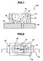
- FIG. 1is a schematic cross-sectional view of a surface mount light-emitting device according to one embodiment of the invention.
- FIG. 2is a schematic plan view of the surface mount light-emitting device of this embodiment.
- FIG. 1is a schematic cross-sectional view taken along lines I-I in FIG. 2 .
- the light-emitting device 100comprises a light-emitting element 10 comprising a gallium nitride compound semiconductor having an emission peak wavelength of 430 nm or longer, and a molded part 40 on which the light-emitting element 10 is disposed.
- the molded part 40preferably uses a cured product of a thermosetting epoxy resin composition comprising (A) an epoxy resin including a triazine derived epoxy resin, (B) an acid anhydride, (C) an antioxidant, (D) a curing catalyst, (E) a reflective member, and (F) an inorganic filler.
- the molded part 40has first and second leads 20 and 30.
- the molded part 40has a recess with a bottom surface and a side surface, and the light-emitting element 10 is disposed on the bottom surface of the recess.
- the light-emitting element 10has a pair of positive and negative electrodes, which are electrically connected to the first and second leads 20 and 30 via wire segments 60.
- the light-emitting element 10is encapsulated with a sealing member 50.
- the sealing member 50is preferably formed of an epoxy resin including a triazine derived epoxy resin or a silicon-containing resin selected from among flexible and rigid silicone resins, a rigid silicone resin, an epoxy-modified silicone resin, a modified silicone resin alone or a mixture of two or more because adhesion to the molded part 40 is then enhanced.
- the sealing member 50contains a phosphor 70 for converting the wavelength of emission from the light-emitting element 10.
- the molded recessed part 40 prepared using a mold or the likehas such a high reflectance as to reduce the transmission of light into the bottom and side surfaces of the recess in the molded part 40 and to increase the release of light toward the front surface.
- the molded part 40is selected to have a high reflection efficiency at 430 nm or longer since the light-emitting element 10 used has an emission peak wavelength of 430 nm or longer. Then the majority of light emitted by the light-emitting element 10 is not absorbed in the molded part 40, but released to the exterior, leading to a high radiant efficiency from the light-emitting element 10. Inversely, if a molded part 40 having a low reflectance is used, the majority of light emitted by the light-emitting element 10 is absorbed in the molded part 40, whereby degradation of the molded part 40 is accelerated.
- the molded part 40 used hereinis a cured product of a thermosetting epoxy resin composition
- a thermosetting epoxy resin compositioncomprising (A) an epoxy resin including a triazine derived epoxy resin, (B) an acid anhydride, (C) an antioxidant, (D) a curing catalyst, (E) a reflective member, and (F) an inorganic filler.
- Aan epoxy resin including a triazine derived epoxy resin
- Ban acid anhydride
- Can antioxidant
- Da curing catalyst
- Ea reflective member
- Fan inorganic filler
- Component (A)is an epoxy resin which contains a triazine derived epoxy resin.
- A-1Triazine derived epoxy resin
- the triazine derived epoxy resinis effective for restraining a cured product of a thermosetting epoxy resin composition from yellowing and for establishing a semiconductor light-emitting device with little degradation with time.
- the triazine derived epoxy resinis preferably a 1,3,5-triazine nucleus derived epoxy resin.
- an epoxy resin having isocyanurate ringshas excellent light resistance and electrical insulation, and should preferably have a divalent, more preferably trivalent epoxy group per isocyanurate ring.
- tris(2,3-epoxypropyl) isocyanurate, tris(a-methylglycidyl) isocyanurate or the likemay be used.
- the triazine derived epoxy resinpreferably has a softening point of 90 to 125°C. It is noted that those resins having hydrogenated triazine rings are excluded from the triazine derived epoxy resin.
- a hydrogenated epoxy resin (A-2)may be used in combination with the triazine derived epoxy resin.
- the hydrogenated epoxy resinis preferably an epoxy resin obtained by hydrogenating an aromatic epoxy resin, and more preferably an epoxy resin having the following general formula (1).
- R 1 and R 2which may be the same or different is a hydrogen atom, methyl group or cyclohexyl group, and n is an integer of 0 to 20.
- the hydrogenated epoxy resin (A-2)preferably has a softening point of 70 to 100°C.
- an epoxy resin (A-3) other than the foregoing (A-1) and (A-2)may be used in combination in an amount below a certain level as long as this does not compromise the effect of the invention.
- exemplary epoxy resinsinclude bisphenol A type epoxy resins, bisphenol F type epoxy resins, biphenol type epoxy resins such as 3,3',5,5'-tetramethyl-4,4'-biphenol type epoxy resins and 4,4'-biphenol type epoxy resins, phenol novolac type epoxy resins, cresol novolac type epoxy resins, bisphenol A novolac type epoxy resins, naphthalene diol type epoxy resins, trisphenylol methane type epoxy resins, tetrakisphenylol ethane type epoxy resins, and epoxy resins obtained through hydrogenation of aromatic rings in phenol dicyclopentadiene novolac type epoxy resins.
- the other epoxy resin (A-3)preferably has a softening point of 70 to 100
- the epoxy resin as component (A)is the triazine derived epoxy resin (A-1) optionally in admixture with the hydrogenated epoxy resin (A-2) and other epoxy resin (A-3).
- Components (A-1) and (A-2)are preferably used in such a proportion as to provide a weight ratio (A-1):(A-2) in the range from 10:0 to 2:8, specifically from 8:2 to 2:8, and more specifically from 7:3 to 3:7. Too high a ratio of hydrogenated epoxy resin (A-2) may lead to a drop of heat resistance and light resistance.
- component (A-3)is preferably admixed in a proportion of up to 30% by weight and more preferably up to 10% by weight, based on the total weight of epoxy resins.
- Component (B)is an acid anhydride which serves as a curing agent. It should preferably be non-aromatic and free of a carbon-carbon double bond in order to provide light resistance.
- exemplary acid anhydridesinclude hexahydrophthalic anhydride, methylhexahydrophthalic anhydride, trialkyltetrahydrophthalic anhydride, and hydrogenated methylnadic anhydride, with the methylhexahydrophthalic anhydride being preferred.
- These acid anhydride curing agentsmay be used alone or in admixture of two or more.
- the acid anhydride curing agentis preferably compounded in an amount to provide 0.5 to 2.0 equivalents and more preferably 0.7 to 1.5 equivalents of acid anhydride per equivalent of the epoxy resin. Less than 0.5 equivalent may result in under-curing and a loss of reliability. If the amount is more than 2.0 equivalents, the unreacted curing agent may be left in the cured product to adversely affect the moisture resistance thereof.
- the preferred amount of the acid anhydride curing agent compoundedis such that 0.6 to 2.0 equivalents, more preferably 1.0 to 2.0 equivalents, and even more preferably 1.2 to 1.6 equivalents of acid anhydride groups are available per equivalent of epoxy groups in the triazine derived epoxy resin. Less than 0.6 equivalent may result in under-curing and a loss of reliability. If the amount is more than 2.0 equivalents, the unreacted curing agent may be left in the cured product to adversely affect the moisture resistance thereof.
- Component (C)is an antioxidant which may be selected from phenol, phosphorus and sulfur based antioxidants. Examples of suitable antioxidants are described below.
- phenol based antioxidantsexamples include 2,6-di-t-butyl-p-cresol, butylated hydroxyanisole, 2,6-di-t-butyl-p-ethylphenol, stearyl- ⁇ -(3,5-dl-t-butyl-4-hydroxyphenyl)propionate, 2,2'-methylenebis(4-methyl-6-t-butylphenol), 4,4'-butylidenebis(3-methyl-6-t-butylphenol), 3,9-bis[1,1-dimethyl-2- ⁇ -(3-t-butyl-4-hydroxy-5-methylphenyl)propionyloxy ⁇ ethyl]-2,4,8,10-tetraoxaspiro[5.5]-undecane, 1,1,3-tris(2-methyl-4-hydroxy-5-t-butylphenyl)butane, and 1,3,5-trimethyl-2,4,6-tris(3,5-di-t-butyl-4-hydroxybenzyl
- phosphorus based antioxidantsinclude triphenyl phosphite, diphenyl alkyl phosphites, phenyl dialkyl phosphites, tri(nonylphenyl) phosphite, trilauryl phosphite, trioctadecyl phosphite, distearyl pentaerythritol diphosphite, tris(2,4-di-tert-butylphenyl)phosphite, diisodecyl pentaerythritol diphosphite, di(2,4-di-tert-butylphenyl) pentaerythritol diphosphite, tristearyl sorbitol triphosphite, and tetrakis(2,4-di-tert-butylphenyl)-4,4'-biphenyl diphosphonate.
- triphenyl phosphitediphen
- sulfur based antioxidantsexamples include dilauryl-3,3'-thiodipropionate, dimyristyl-3,3'-thiodipropionate, and distearyl-3,3'-thiodipropionate.
- antioxidantsmay be used alone.
- a phosphorus based antioxidantis used alone, or a phenol based antioxidant and a phosphorus based antioxidant are used in combination.
- the phenol based antioxidant and the phosphorus based antioxidantare used in such a proportion that a weight ratio of phenol based antioxidant to phosphorus based antioxidant is in the range from 0:100 to 70:30, and more preferably from 0:160 to 50:50.
- the antioxidantis preferably compounded in an amount of 0.01 to 10 parts, and more preferably 0.03 to 5 parts by weight per 100 parts by weight of the epoxy resin composition. Too less an amount of the antioxidant may fail to achieve sufficient heat resistance and allow for discoloration. Too much the antioxidant may become cure-inhibitory, failing to acquire sufficient cure and strength.
- Component (D)is a curing catalyst which may be selected from well-known curing catalysts used in epoxy resin compositions.
- exemplary curing catalystsinclude, but are not limited to, tertiary amines, imidazoles, and organic carboxylic acid salts thereof, organic carboxylic acid metal salts, metal-organic chelate compounds, aromatic sulfonium salts, organic phosphine compounds, and salts thereof, which may be used alone or in admixture.
- imidazoles and phosphorus based curing catalystsare more preferred, for example, 2-ethyl-4-methylimidazole, methyl-tributylphosphonium-dimethyl phosphate, and quaternary phosphonium bromide.
- the cure acceleratoris preferably used in an amount of 0.05 to 5%, and more preferably 0.1 to 2% by weight based on the entire composition. Outside the range, the cured product of the epoxy resin composition may lose a balance of heat resistance and moisture resistance.
- components (A), (B) and (C)should be previously melt mixed at 70 to 120°C. preferably 80 to 110°C, to form a solid material having a softening point of 50 to 100°C, preferably 60 to 90°C, and the solid material be ground prior to compounding. If the material obtained by melt mixing has a softening point below 50°C, it does not become solid. A softening point above 100°C leads to a loss of flow.
- the triazine derived epoxy resin (A-1)is used alone as component (A), components (A-1) and (B), preferably components (A-1), (B) and (C) are previously reacted at 70 to 120°C, preferably 80 to 110°C, for 4 to 20 hours, preferably 6 to 15 hours, or components (A-1), (B) and (D), preferably components (A-1), (B), (C) and (D) are previously reacted at 30 to 80°C, preferably 40 to 60° C, for 10 to 72 hours, preferably 36 to 60 hours, to form a solid material having a softening point of 50 to 100°C, and preferably 60 to 90°C, and the solid material is ground prior to compounding. If the material resulting from reaction has a softening point below 50°C, it may not become solid. A softening point above 100°C may lead to a loss of flow.
- the materialmay not become solid due to a low content of high molecular weight fraction. If the reaction time is too long, the flow may become less.
- the solid reaction product obtained hereinis preferably the reaction product of the triazine derived epoxy resin as component (A) with the acid anhydride as component (B), which contains a high molecular weight fraction having a molecular weight of more than 1500, a moderate molecular weight fraction having a molecular weight of 300 to 1500, and a monomeric fraction, as analyzed by gel permeation chromatography (GPC) (under analytical conditions: sample concentration 0.2 wt%, feed volume 50 ⁇ L, mobile phase THF 100%, flow rate 1.0 mL/min, temperature 40°C, and a detector RI), wherein 20 to 70% by weight of the high molecular weight fraction, 10 to 60% by weight of the moderate molecular weight fraction, and 10 to 40% by weight of the monomeric fraction are present.
- GPCgel permeation chromatography
- the solid reaction product mentioned abovecontains a reaction product represented by the following formula (2), and especially a reaction product represented by the following formula (3) when the acid anhydride as component (B) is methylhexahydrophthalic anhydride.
- Ris an acid anhydride residue
- nis an arbitrary number in the range of 0 to 200.
- the reaction producthas an average molecular weight of 500 to 100,000.
- the solid reaction product according to the inventionpreferably contains 20 to 70%, especially 30 to 60% by weight of a high molecular weight fraction with a molecular weight of more than 1500, 10 to 60%, especially 10 to 40% by weight of a moderate molecular weight fraction with a molecular weight of 300 to 1500, and 10 to 40%, especially 15 to 30% by weight of a monomeric fraction (unreacted epoxy resin and acid anhydride).
- the epoxy resin composition of the inventioncontains the resin component obtained by the above-mentioned procedure. If the antioxidant (C) and the curing catalyst (D) are not used during the preparation of the resin component, the antioxidant (C) and the curing catalyst (D) are preferably compounded with the resin component at the stage when the epoxy resin composition is prepared. In the epoxy resin composition, the following components may be further compounded.
- titanium dioxideis especially preferred, although barium titanate, zinc oxide and the like may also be used. Titanium dioxide is compounded as a white colorant for enhancing whiteness and has a unit lattice which may be either rutile or anatase type. It is not limited in average particle size and shape.
- the titanium dioxidemay be previously surface treated with hydrous oxides of aluminum, silicon or the like for enhancing its compatibility with and dispersibility in resins and inorganic fillers.
- An amount of titanium dioxide loadedis preferably 2 to 80% by weight and more preferably 5 to 50% by weight of the entire composition. Less than 2% by weight may fail to achieve a sufficient whiteness whereas more than 80% by weight may adversely affect molding properties, leaving unfilled or void defects.
- any fillers other than component (E) commonly compounded in epoxy resin compositionsmay be used.
- examplesinclude silicas such as fused silica and crystalline silica, alumina, silicon nitride, aluminum nitride, boron nitride, glass fibers, and antimony trioxide. These inorganic fillers are not particularly limited in average particle size and shape.
- the inorganic filler which has been surface treated with coupling agentssuch as silane coupling agents and titanate coupling agents may be compounded for enhancing the bond strength between the resin and the inorganic filler.
- Suitable and preferable coupling agentsinclude, for example, epoxy functional alkoxysilanes such as ⁇ -glycidoxypropyltrimethoxysilane, ⁇ -glycidoxypropylmethyldiethoxysilane, and ⁇ -(3,4-epoxycyclohexyl)ethyltrimethoxysilane, amino functional alkoxysilanes such as N- ⁇ -(aminoethyl)- ⁇ -aminopropyltrimethoxysilane, ⁇ -aminopropyltriethoxysilane, and N-phenyl-y-aminopropyltrimethoxysilane, and mercapto functional alkoxysilanes such as ⁇ -mercaptopropyltrimethoxysilane. It is understood that the amount of the coupling agent used for surface treatment and the surface treatment technique are not particularly limited.
- An amount of the inorganic filler addedis preferably 20 to 700 parts by weight and more preferably 50 to 400 parts by weight per 100 parts by weight of the epoxy resin (A) and the acid anhydride (B) combined. Less than 20 pbw may fail to achieve a sufficient strength whereas more than 700 pbw may result in unfilled defects due to a viscosity buildup and failures such as separation within the device or package due to a loss of flexibility.
- the inorganic filleris preferably contained in an amount of 10 to 90% by weight and more preferably 20 to 80% by weight based on the entire composition.
- various additivesmay be compounded if necessary.
- various stress-reducing agentssuch as thermoplastic resins, thermoplastic elastomers, organic synthetic rubbers and silicones, waxes, halogen trapping agents, and other additives may be added and compounded for the purpose of improving certain properties of the resin insofar as this does not compromise the effects of the invention.
- the epoxy resin composition of the inventionis prepared as a molding compound, preferably by previously combining components (A), (B) and (C) together, uniformly melt mixing them at a temperature in the range of 70 to 120°C, and preferably 80 to 110°C on a suitable equipment such as a solventless reactor which can be heated, until the mixture undergoes a viscosity buildup to reach a softening point sufficient to handle at room temperature, specifically of 50 to 100°C and preferably 60 to 90°C, then cooling the mixture into a solid mixture. It is noted that where components (A-1).
- the mixing temperatureis too low, it fails to form a mixture which becomes solid at room temperature. If the mixing temperature is too high, too high a reaction rate makes it difficult to terminate the reaction at then desired extent of reaction.
- the mixtureis ground, following which components (E) and (F) and other additives are compounded in predetermined formulation ratios.
- the resulting mixtureis fully uniformly mixed on a mixer or the like, then melt mixed on a hot roll mill, kneader or extruder, cooled for solidification, and comminuted into a suitable size.
- the resulting epoxy resin compositionis ready for use as molding compound.
- the white epoxy resin composition of the inventionthus obtained may be advantageously utilized as molded parts in semiconductor and electronic equipment, especially using light-emitting elements, or encapsulants for light-emitting elements and other semiconductor devices. Excluded are light-sensing elements and photo-couplers having light-emitting and sensing elements integrated.
- the encapsulation method which is most generally used in this applicationis low-pressure transfer molding.
- the epoxy resin composition of the inventionis desirably molded at a temperature of 150 to 185°C for 30 to 180 seconds. Post-cure may be effected at 150 to 195°C for 2 to 20 hours.
- the light-emitting element 10 used hereinshould have an emission peak wavelength of 430 nm or longer because the molded part 40 exhibits a high reflectance and possesses light resistance at or above that wavelength.
- Use of a gallium nitride compound semiconductoris particularly preferred.
- a light-emitting device of the prior art construction that a light-emitting element comprising a gallium nitride compound semiconductor is disposed on a molded part of PPShas the problem that the molded part can be degraded by the heat release from the light-emitting element because the light-emitting elements of gallium nitride compound semiconductor produce more amounts of heat upon electric current conduction than light-emitting elements of GaP, GaAs or the like.
- the light-emitting element 10 of gallium nitride compound semiconductor used hereinis prepared by depositing a semiconductor such as GaN, InGaN, or InAlGaN on a substrate to form a light-emitting layer.
- the sealing member 50is preferably formed using an epoxy resin including a triazine derived epoxy resin or a silicon-containing resin as typified by a silicone resin.
- the sealing member 50 using an epoxy resin including a triazine derived epoxy resinoffers enhanced adhesion since it is of the same material system as the molded part 40. Since the light-emitting element 10 of gallium nitride compound semiconductor reaches a temperature of at least 100°C upon electric current conduction, both the sealing member 50 and the molded part 40 are thermally expanded, though to a slight extent. When the sealing member 50 and the molded part 40 are formed of materials of the same system, they have approximate coefficients of thermal expansion so that little separation occurs at the interface between the sealing member 50 and the molded part 40.
- sealing members using silicon-containing resinstend to be less adherent to prior art molded parts using thermoplastic resins, their adhesion can be increased when the molded part 40 is made of the epoxy resin composition of the invention. Since the light-emitting element 10 of gallium nitride compound semiconductor emits blue light having a high level of emission energy upon electric current application, the sealing member in close contact with the light-emitting element 10 is most prone to degradation. The rate of degradation can be minimized by forming the sealing member from silicon-containing resins, typically silicone resins.
- the adhesion interface between the sealing member of light resistant silicon-containing resin and the molded part of the inventive epoxy resin compositionis least prone to failure.
- the sealing member 50 used hereinmay be a member formed from a cured product of a thermosetting epoxy resin composition
- a thermosetting epoxy resin compositioncomprising (A) an epoxy resin including a triazine derived epoxy resin, (B) an acid anhydride, (C) an antioxidant, and (D) a curing catalyst, wherein components (A), (B) and (C) are compounded as a solid material in ground form obtained by previously melt mixing components (A), (B) and (C) at 70 to 120°C to form a solid mixture having a softening point of 50 to 100°C and grinding the mixture.
- the phosphor 70may be any of compounds which absorb light from the light-emitting element 10 and wavelength convert it into light of a different wavelength.
- Usemay be made of, for example, rare earth based aluminate salt phosphors activated mainly with a lanthanoid element like Ce, such as represented by Y 3 Al 5 O 12 :Ce, (Y,Gd) 3 Al 5 O 12 :Ce, and Y 3 (Al,Ga) 5 O 12 :Ce.
- the epoxy resin, acid anhydride and antioxidantwere previously melt mixed on a reactor at 100°C for 3 hours.
- the mixturewas cooled for solidification (softening point 60°C), ground, and thereafter compounded with other components in the predetermined compositional ratio.
- Thiswas uniformly melt mixed on a hot twin-roll mill, cooled, and ground, yielding a cured product of a white epoxy resin composition serving as a molded part for use in a light-emitting device.
- the starting materials used hereinare described below.
- a viscositywas measured at a temperature of 175°C and a load of 10 kgf.
- a cured partwas formed at 175°C and 6.9 N/mm 2 for a molding time of 120 seconds using a mold according to EMMI standards, and measured for flexural strength according to JIS K-6911.
- a disk having a diameter of 50 mm and a thickness of 3 mmwas molded at 175°C and 6.9 N/mm 2 for a molding time of 2 minutes and allowed to stand at 180°C for 24 hours, after which yellowness was compared.
- Examples 1 to 5 wherein components (A), (B) and (C) were premixedare improved in many properties over Examples 6 and 7 wherein they were not premixed.
- Examples 1 to 5 wherein component (B) is an acid anhydride which is non-aromatic and free of a carbon-carbon double bondare improved in many properties over Example 8 wherein component (B) has a carbon-carbon double bond.
- Examples 1 to 5 using component (A-1) and/or (A-2)are improved in many properties over Examples 9 and 10 using component (A-3).
- Examples 1 to 5remain white in the heat resistance or yellowing test whereas Examples 6 to 10 yellow. Therefore, Examples 1 to 5 are highly heat resistant and their molded parts are found undegraded.
- FIG. 3is a diagram showing a reflectance of a molded part. It is seen that the molded part exhibits a very high reflectance to light having wavelengths of 430 nm or longer.
- Example 11demonstrates a light-emitting device.
- an epoxy resin composition according to the inventionis molded to form a molded part on a leadframe of copper alloy by a transfer molding technique.
- the molded partis provided with a recess having bottom and side surfaces.
- a light-emitting element of blue emissioncomprising a sapphire substrate and a light-emitting layer of InGaN is mounted using an epoxy resin adhesive.
- the light-emitting elementis electrically connected to the leadframe using gold wires having a diameter of 30 ⁇ m.
- a sealing memberis applied dropwise into the molded part with the recess on the bottom surface of which the light-emitting element is mounted.
- the sealing member usedcontains 100 parts by weight of a silicone resin, 30 parts by weight of a YAG phosphor, and 5 parts by weight of a light diffuser of silicon oxide. It is heated from room temperature to 150°C over 3 hours, and cured at 150°C for 5 hours. Finally, the frame is cut out, yielding a light-emitting device of white emission.
- Comparative Example 1demonstrates a light-emitting device.
- PPSpolyphenylene sulfide
- a light-emitting element of blue emissioncomprising a sapphire substrate and a light-emitting layer of InGaN is mounted using an epoxy resin adhesive.
- the light-emitting elementis electrically connected to the leadframe using gold wires having a diameter of 30 ⁇ m.
- a sealing memberis applied dropwise into the molded part with the recess on the bottom surface of which the light-emitting element is mounted.
- the sealing member usedcontains 100 parts by weight of a silicone resin, 30 parts by weight of a YAG phosphor, and 5 parts by weight of a light diffuser of silicon oxide. It is heated from room temperature to 150°C over 3 hours, and cured at 150°C for 5 hours. Finally, the frame is cut out, yielding a light-emitting device of white emission.
- Example 11 and Comparative Example 1were compared for performance and outer appearance when a current flow of 150 mA was conducted for 500 hours at room temperature.
- the relative outputis an output after 500-hour current conduction relative to an output before current conduction which is 100%.
- the relative outputis determined by measuring five samples for each of Example 11 and Comparative Example 1 and calculating an average thereof.
- the percent separation (or delamination) between molded part and sealing memberis 0% when no separation occurred, and 100% when separation occurred along the entire interface.
- the separation between molded part and sealing memberis reported when any separation is detectable even at a part of the interface between the molded part and the sealing member.
- the percent separationindicates the number of separated samples among 100 samples prepared for each of Example 11 and Comparative Example 1. It is thus seen that Example 11 is substantially better in heat resistance, light resistance and adhesion than Comparative Example 1.
- An epoxy resin compositionwas prepared by melt mixing the reactive components selected from the components shown in Table 3 under the conditions shown in Table 3, grinding the solid reaction product thus obtained, and compounding it with the remaining components.
- the solid reaction product and the cured product obtained by curing the epoxy resin composition on a transfer molding machinewere examined for properties by the following methods. The results are also shown in Table 3.
- the solid reaction productwas analyzed by GPC under the following conditions. Using a chromatograph HLC-8120 (Tosoh Corp.) equipped with TSK guard columns HXL-L+G4, 3, 2, 2HxL, analysis was performed under conditions: a sample concentration 0.2%, a feed volume 50 ⁇ L, a mobile phase THF 100%, a flow rate 1.0 mL/min, a temperature 40°C, and a detector RI. From the GPC analysis data, the ratios of TEPIC monomer, MH monomer, moderate molecular weight fraction, and high molecular weight fraction were computed. The fraction ratio values in Table 3 are by weight.
- compositionwas examined and evaluated for gel time, yellowing, thermogravimetric-differential thermal analysis (TG-DTA) and strength.
- a sample1.0 g was placed on a hot plate at 175°C, and at the same time measurement was started with a stopwatch. The sample on the hot plate was scraped, detecting the time when the sample started gelation.
- the cured samplewas held at 180°C for 24 hours, after which it was examined for yellowing again.
- Analysiswas performed by molding a sample at 180°C for 60 seconds into a disc specimen having a diameter of 10 mm and a height of 2 mm, heating at a rate of 5°C/min from room temperature to 500°C, obtaining a thermogravimetric curve, and determining the temperature corresponding to a weight loss of 0.2% from the curve.
- a samplewas molded at 180°C for 60 seconds into a specimen of 50 ⁇ 10 ⁇ 0.5 mm.
- Three-point flexural strengthwas measured at room temperature and a test speed of 2 mm/sec.
- the solid reaction products of Examples 12 to 15contain a compound having the following formula with a molecular weight of more than 1,500, a compound having the following formula with a molecular weight of 300-1,500, and the monomers in proportions X, Y, and Z (expressed by weight), respectively.
- compositions which have not been B-stagedare applicable in some cases, B-staged compositions are preferred in the practice of the invention. This is because B-staged compositions are prone to yellowing and maintain a high strength.
- the light-emitting device of the inventioncan be utilized as luminaires, displays, mobile phone backlights, moving picture illuminating auxiliary light sources, and other general commercial light sources.
Landscapes
- Chemical & Material Sciences (AREA)
- Health & Medical Sciences (AREA)
- Chemical Kinetics & Catalysis (AREA)
- Medicinal Chemistry (AREA)
- Polymers & Plastics (AREA)
- Organic Chemistry (AREA)
- Led Device Packages (AREA)
- Epoxy Resins (AREA)
- Compositions Of Macromolecular Compounds (AREA)
- Injection Moulding Of Plastics Or The Like (AREA)
- Structures Or Materials For Encapsulating Or Coating Semiconductor Devices Or Solid State Devices (AREA)
Description
- This invention relates to a light-emitting device for use as luminaires, displays, mobile phone backlights, moving picture illuminating auxiliary light sources, and other general commercial light sources, a method for preparing the same, a molded part, and a sealing member.
- Surface mount light-emitting devices using light-emitting elements feature a small size, a good power efficiency, and light emission of brilliant color. The light-emitting elements eliminate the risk of lamp failures since they are semiconductor elements. They are also characterized by improved initial drive performance and resistance to vibration and repeated turn-on and off. Because of these improved properties, light-emitting devices using light-emitting elements such as light-emitting diodes (LED) and laser diodes (LD) are utilized as light sources in varying applications. Recently, light-emitting elements have marked a rapid advance toward higher outputs.
For the surface mount light-emitting devices, thermoplastic resins such as liquid crystal polymers, polyphenylene sulfide (PPS) and nylon are often used as molded parts due to ease of mass-scale production.
On the other hand, epoxy resins are used in sealing members for protecting the light-emitting elements from moisture, dust and contaminants (see, for example, Patent Reference 1:JP 3512732 JP-A 2001-234032 JP-A 2002-302533
Also silicone resins are used as the output of light-emitting elements is increased. - However, prior art thermoplastic resins used as moldings in surface mount light-emitting devices are less resistant to light due to the inclusion of an aromatic component within the molecule although they are resistant to heat. Also, since hydroxyl groups or other groups for improving adhesion are absent at molecular ends, the resins exhibit poor adhesion to leads and sealing members. In particular, sealing members using silicone resins lack long-term reliability since they show a drastic drop in adhesion to molded parts using thermoplastic resins, as compared with sealing members using epoxy resins.
Epoxy resins are used as sealing members, but not as molded parts in leadframe type surface mount devices because of their difficulty to mold.
Also, light-emitting elements of gallium nitride compound semiconductor capable of blue emission produce higher outputs than light-emitting elements capable of red emission and also generate more amounts of heat. Thus, degradation of molded parts becomes a problem when light-emitting elements of blue emission are used. - Also,
JP 2656336 JP 2656336 - In this regard,
JP-A 2000-196151 JP-A 2003-224305 JP-A 2005-306952 - Known references relating to the present invention include the foregoing and
Patent References 8 and 9 and Non-Patent Reference 1, listed below.Patent Reference 1: JP 3512732 Patent Reference 2: JP-A 2001-234032 Patent Reference 3: JP-A 2002-302533 Patent Reference 4: JP 2656336 Patent Reference 5: JP-A 2000-196151 Patent Reference 6: JP-A 2003-224305 Patent Reference 7: JP-A 2005-306952 Patent Reference 8: JP-A 2005-259972 Patent Reference 9: JP-A 2006-156704 Non-Patent Reference 1: Electronics Mount Technology, April 2004 JP-A-2004-172636 - According an object of the invention is to provide a light-emitting device device using a molded part with improved heat resistance and light resistance, and a method for preparing the same. Another object of the invention is to provide a molded part and a sealing member for use in a light-emitting device.
The invention is defined in claims 1 and 11. Preferred features of the invention are set out in the dependent claims. - Making extensive investigations to solve the outstanding problems, the inventor have completed the present invention.
One aspect of the invention relates to a light-emitting device comprising a light-emitting element comprising a gallium nitride compound semiconductor having an emisision peak wavelength of 430 nm or longer, and a molded part on which the light-emitting element is disposed, the molded part using a cured product of a thermosetting epoxy resin composition comprising an epoxy resin including a triazine derived epoxy resin. A light-emitting device with improved heat resistance and light resistance is then provided even when the light-emitting element comprising a gallium nitride compound semiconductor is use. - The molded part is preferably a cured product of a thermosetting epoxy resin composition comprising (A) the epoxy resin including a triazine derived epoxy resin, and further comprising (B) an acid anhydride, (C) an antioxidant, (D) a curing catalyst, (E) a reflective member, and (F) an inorganic filler. This molded part has a good curability, improved heat resistance and light resistance, and a satisfactory strength.
The thermosetting epoxy resin composition preferably comprises a solid material in ground form obtained by melt mixing (A) the epoxy resin including a triazine derived epoxy resin with (B) an acid anhydride and (C) an antioxidant. The composition is then improved in flexural strength. - In this embodiment, the thermosetting epoxy resin composition preferably comprises as a resin component a solid material in ground form obtained by reacting a triazine derived epoxy resin with an acid anhydride in such a proportion as to provide an epoxy group equivalent/acid anhydride group equivalent ratio from 0.6 to 2.0. More preferably, the reaction of a triazine derived epoxy resin with an acid anhydride is effected in the presence of an antioxidant; or the reaction of a triazine derived epoxy resin with an acid anhydride is effected in the presence of a curing catalyst or a curing catalyst and an antioxidant. Also preferably, the thermosetting epoxy resin composition further comprises (E) a reflective member and (F) an inorganic filler.
- The molded part preferably has a reflectance of at least 70% at 430 nm or longer. A light-emitting device featuring a high radiation efficiency from the light-emitting element is then available.
Preferably the molded part has a recess with a bottom surface and a side surface, the light-emitting element is disposed on the bottom surface of the recess, and the light-emitting element is sealed with a sealing member comprising an epoxy resin including a triazine derived epoxy resin or a silicon-containing resin. Then adhesion to the molded part is significantly improved. - Another aspect of the invention relates to a light-emitting device comprising a light-emitting element having an emission peak wavelength of 430 nm or longer, and a molded part on which the light-emitting element is disposed, the molded part using a cured product of a thermosetting epoxy resin composition comprising an epoxy resin including a triazine derived epoxy resin, an acid anhydride, a reflective member, and a curing catalyst as essential components. A light-emitting device with improved heat resistance and light resistance is then provided. Also in this embodiment, the epoxy resin including a triazine derived epoxy resin and the acid anhydride are preferably compounded in the thermosetting epoxy resin composition as a solid material in ground form obtained by reacting the triazine derived epoxy resin with the acid anhydride in such a proportion as to provide an epoxy group equivalent/acid anhydride group equivalent ratio from 0.6 to 2.0. More preferably, the reaction of the triazine derived epoxy resin with the acid anhydride is effected in the presence of an antioxidant; or the reaction of the triazine derived epoxy resin with the acid anhydride is effected in the presence of the curing catalyst or the curing catalyst and an antioxidant, so that the curing catalyst is also compounded as the solid material in ground form.
- A further aspect of the invention relates to a method for preparing a light-emitting device comprising the first step of mixing a solid material in ground form obtained by melt mixing (A) an epoxy resin including a triazine derived epoxy resin with (B) an acid anhydride and (C) an antioxidant, with (D) a curing catalyst, (E) a reflective member, and (F) an inorganic filler, the second step of molding a thermosetting epoxy resin composition resulting from the first step in a mold with leads arranged in place by a transfer molding technique, and the third step of disposing a light-emitting element on the leads on a cured product of the thermosetting epoxy resin composition resulting from the second step. Then a light-emitting device using a molded part in the form of a cured product of a thermosetting epoxy resin composition is readily provided.
- Also provided is a method for preparing a light-emitting device comprising the first step of mixing a solid material in ground form obtained by reacting a triazine derived epoxy resin with an acid anhydride in such a proportion as to provide an epoxy group equivalent/acid anhydride group equivalent ratio from 0.6 to 2.0, with (D) a curing catalyst, (E) a reflective member, and (F) an inorganic filler, the second step of molding a thermosetting epoxy resin composition resulting from the first step in a mold with leads arranged in place by a transfer molding technique, and the third step of disposing a light-emitting element on the leads on a cured product of the thermosetting epoxy resin composition resulting from the second step. Preferably in this embodiment, the reaction of the triazine derived epoxy resin with the acid anhydride is effected in the presence of an antioxidant; or the reaction of the triazine derived epoxy resin with the acid anhydride is effected in the presence of the curing catalyst or the curing catalyst and an antioxidants, so that the curing catalyst is also compounded as the solid material in ground form.
- A still further aspect of the invention relates to a molded part for use in a light-emitting device, formed from a cured product of a thermosetting epoxy resin composition comprising (A) an epoxy resin including a triazine derived epoxy resin, (B) an acid anhydride, (C) an antioxidant, (D) a curing catalyst, (E) a reflective member, and (F) an inorganic filler, components (A), (B) and (C) being compounded as a solid material in ground form obtained by melt mixing them. A molded part having improved heat resistance and light resistance is then provided.
- A still further aspect of the invention relates to a sealing member for use in a light-emitting device, formed from a cured product of a thermosetting epoxy resin composition comprising (A) an epoxy resin including a triazine derived epoxy resin, (B) an acid anhydride, (C) an antioxidant, and (D) a curing catalyst, components (A), (B) and (C) being compounded as a solid material in ground form obtained by melt mixing them. A sealing member having improved heat resistance and light resistance is then provided.
It is noted that photo-couplers are not encompassed within the scope of the invention and should be excluded. - The light-emitting device of the invention has improved heat resistance, light resistance and adhesion. The molded part on which a light-emitting element is disposed is improved in curability, has a satisfactory strength, and maintains heat resistance, light resistance and adhesion over a long term. The sealing member gives a cured product which is uniform and generates little variation in color.
FIG. 1 is a schematic cross-sectional view of a surface mount light-emitting device according to one embodiment of the invention.FIG. 2 is a schematic plan view of the surface mount light-emitting device of the embodiment.FIG. 3 is a diagram showing a reflectance of a molded part according to another embodiment of the invention.- Now, the light-emitting device, molded part, sealing member and methods for preparing them are described by referring to their embodiments and examples. It is understood that the invention is not limited to the embodiments and examples illustrated herein. A surface mount light-emitting device according to one embodiment of the invention is described with reference to the figures.
FIG. 1 is a schematic cross-sectional view of a surface mount light-emitting device according to one embodiment of the invention.FIG. 2 is a schematic plan view of the surface mount light-emitting device of this embodiment.FIG. 1 is a schematic cross-sectional view taken along lines I-I inFIG. 2 . - The light-emitting
device 100 comprises a light-emittingelement 10 comprising a gallium nitride compound semiconductor having an emission peak wavelength of 430 nm or longer, and a moldedpart 40 on which the light-emittingelement 10 is disposed. The moldedpart 40 preferably uses a cured product of a thermosetting epoxy resin composition comprising (A) an epoxy resin including a triazine derived epoxy resin, (B) an acid anhydride, (C) an antioxidant, (D) a curing catalyst, (E) a reflective member, and (F) an inorganic filler. The moldedpart 40 has first and second leads 20 and 30. The moldedpart 40 has a recess with a bottom surface and a side surface, and the light-emittingelement 10 is disposed on the bottom surface of the recess. The light-emittingelement 10 has a pair of positive and negative electrodes, which are electrically connected to the first and second leads 20 and 30 viawire segments 60. The light-emittingelement 10 is encapsulated with a sealingmember 50. The sealingmember 50 is preferably formed of an epoxy resin including a triazine derived epoxy resin or a silicon-containing resin selected from among flexible and rigid silicone resins, a rigid silicone resin, an epoxy-modified silicone resin, a modified silicone resin alone or a mixture of two or more because adhesion to the moldedpart 40 is then enhanced. Notably, encapsulation with another epoxy resin or urethane resin is possible. The sealingmember 50 contains aphosphor 70 for converting the wavelength of emission from the light-emittingelement 10. The molded recessedpart 40 prepared using a mold or the like has such a high reflectance as to reduce the transmission of light into the bottom and side surfaces of the recess in the moldedpart 40 and to increase the release of light toward the front surface. - The molded
part 40 is selected to have a high reflection efficiency at 430 nm or longer since the light-emittingelement 10 used has an emission peak wavelength of 430 nm or longer. Then the majority of light emitted by the light-emittingelement 10 is not absorbed in the moldedpart 40, but released to the exterior, leading to a high radiant efficiency from the light-emittingelement 10. Inversely, if a moldedpart 40 having a low reflectance is used, the majority of light emitted by the light-emittingelement 10 is absorbed in the moldedpart 40, whereby degradation of the moldedpart 40 is accelerated. - The molded
part 40 used herein is a cured product of a thermosetting epoxy resin composition comprising (A) an epoxy resin including a triazine derived epoxy resin, (B) an acid anhydride, (C) an antioxidant, (D) a curing catalyst, (E) a reflective member, and (F) an inorganic filler. The respective components are described below. - Component (A) is an epoxy resin which contains a triazine derived epoxy resin.
- The triazine derived epoxy resin is effective for restraining a cured product of a thermosetting epoxy resin composition from yellowing and for establishing a semiconductor light-emitting device with little degradation with time. The triazine derived epoxy resin is preferably a 1,3,5-triazine nucleus derived epoxy resin. In particular, an epoxy resin having isocyanurate rings has excellent light resistance and electrical insulation, and should preferably have a divalent, more preferably trivalent epoxy group per isocyanurate ring. Specifically, tris(2,3-epoxypropyl) isocyanurate, tris(a-methylglycidyl) isocyanurate or the like may be used.
The triazine derived epoxy resin preferably has a softening point of 90 to 125°C. It is noted that those resins having hydrogenated triazine rings are excluded from the triazine derived epoxy resin. - A hydrogenated epoxy resin (A-2) may be used in combination with the triazine derived epoxy resin. The hydrogenated epoxy resin is preferably an epoxy resin obtained by hydrogenating an aromatic epoxy resin, and more preferably an epoxy resin having the following general formula (1).

- It is noted that the hydrogenated epoxy resin (A-2) preferably has a softening point of 70 to 100°C.
- Also, if necessary, an epoxy resin (A-3) other than the foregoing (A-1) and (A-2) may be used in combination in an amount below a certain level as long as this does not compromise the effect of the invention. Exemplary epoxy resins include bisphenol A type epoxy resins, bisphenol F type epoxy resins, biphenol type epoxy resins such as 3,3',5,5'-tetramethyl-4,4'-biphenol type epoxy resins and 4,4'-biphenol type epoxy resins, phenol novolac type epoxy resins, cresol novolac type epoxy resins, bisphenol A novolac type epoxy resins, naphthalene diol type epoxy resins, trisphenylol methane type epoxy resins, tetrakisphenylol ethane type epoxy resins, and epoxy resins obtained through hydrogenation of aromatic rings in phenol dicyclopentadiene novolac type epoxy resins.
It is noted that the other epoxy resin (A-3) preferably has a softening point of 70 to 100°C. - The epoxy resin as component (A) is the triazine derived epoxy resin (A-1) optionally in admixture with the hydrogenated epoxy resin (A-2) and other epoxy resin (A-3). Components (A-1) and (A-2) are preferably used in such a proportion as to provide a weight ratio (A-1):(A-2) in the range from 10:0 to 2:8, specifically from 8:2 to 2:8, and more specifically from 7:3 to 3:7. Too high a ratio of hydrogenated epoxy resin (A-2) may lead to a drop of heat resistance and light resistance. Also, component (A-3) is preferably admixed in a proportion of up to 30% by weight and more preferably up to 10% by weight, based on the total weight of epoxy resins.
- Component (B) is an acid anhydride which serves as a curing agent. It should preferably be non-aromatic and free of a carbon-carbon double bond in order to provide light resistance. Exemplary acid anhydrides include hexahydrophthalic anhydride, methylhexahydrophthalic anhydride, trialkyltetrahydrophthalic anhydride, and hydrogenated methylnadic anhydride, with the methylhexahydrophthalic anhydride being preferred. These acid anhydride curing agents may be used alone or in admixture of two or more.
- The acid anhydride curing agent is preferably compounded in an amount to provide 0.5 to 2.0 equivalents and more preferably 0.7 to 1.5 equivalents of acid anhydride per equivalent of the epoxy resin. Less than 0.5 equivalent may result in under-curing and a loss of reliability. If the amount is more than 2.0 equivalents, the unreacted curing agent may be left in the cured product to adversely affect the moisture resistance thereof.
- In this regard, where only the triazine derived epoxy resin (A-1) is used as component (A), the preferred amount of the acid anhydride curing agent compounded is such that 0.6 to 2.0 equivalents, more preferably 1.0 to 2.0 equivalents, and even more preferably 1.2 to 1.6 equivalents of acid anhydride groups are available per equivalent of epoxy groups in the triazine derived epoxy resin. Less than 0.6 equivalent may result in under-curing and a loss of reliability. If the amount is more than 2.0 equivalents, the unreacted curing agent may be left in the cured product to adversely affect the moisture resistance thereof.
- Component (C) is an antioxidant which may be selected from phenol, phosphorus and sulfur based antioxidants. Examples of suitable antioxidants are described below.
- Examples of phenol based antioxidants include 2,6-di-t-butyl-p-cresol, butylated hydroxyanisole, 2,6-di-t-butyl-p-ethylphenol, stearyl-β-(3,5-dl-t-butyl-4-hydroxyphenyl)propionate, 2,2'-methylenebis(4-methyl-6-t-butylphenol), 4,4'-butylidenebis(3-methyl-6-t-butylphenol), 3,9-bis[1,1-dimethyl-2-{β-(3-t-butyl-4-hydroxy-5-methylphenyl)propionyloxy}ethyl]-2,4,8,10-tetraoxaspiro[5.5]-undecane, 1,1,3-tris(2-methyl-4-hydroxy-5-t-butylphenyl)butane, and 1,3,5-trimethyl-2,4,6-tris(3,5-di-t-butyl-4-hydroxybenzyl)-benzene. Inter alia, 2,6-di-t-butyl-p-cresol is preferred.
- Examples of phosphorus based antioxidants include triphenyl phosphite, diphenyl alkyl phosphites, phenyl dialkyl phosphites, tri(nonylphenyl) phosphite, trilauryl phosphite, trioctadecyl phosphite, distearyl pentaerythritol diphosphite, tris(2,4-di-tert-butylphenyl)phosphite, diisodecyl pentaerythritol diphosphite, di(2,4-di-tert-butylphenyl) pentaerythritol diphosphite, tristearyl sorbitol triphosphite, and tetrakis(2,4-di-tert-butylphenyl)-4,4'-biphenyl diphosphonate. Inter alia, triphenyl phosphite is preferred.
- Examples of sulfur based antioxidants include dilauryl-3,3'-thiodipropionate, dimyristyl-3,3'-thiodipropionate, and distearyl-3,3'-thiodipropionate.
- These antioxidants may be used alone. Preferably a phosphorus based antioxidant is used alone, or a phenol based antioxidant and a phosphorus based antioxidant are used in combination. In this regard, the phenol based antioxidant and the phosphorus based antioxidant are used in such a proportion that a weight ratio of phenol based antioxidant to phosphorus based antioxidant is in the range from 0:100 to 70:30, and more preferably from 0:160 to 50:50.
- The antioxidant is preferably compounded in an amount of 0.01 to 10 parts, and more preferably 0.03 to 5 parts by weight per 100 parts by weight of the epoxy resin composition. Too less an amount of the antioxidant may fail to achieve sufficient heat resistance and allow for discoloration. Too much the antioxidant may become cure-inhibitory, failing to acquire sufficient cure and strength.
- Component (D) is a curing catalyst which may be selected from well-known curing catalysts used in epoxy resin compositions. Exemplary curing catalysts include, but are not limited to, tertiary amines, imidazoles, and organic carboxylic acid salts thereof, organic carboxylic acid metal salts, metal-organic chelate compounds, aromatic sulfonium salts, organic phosphine compounds, and salts thereof, which may be used alone or in admixture. Of these, imidazoles and phosphorus based curing catalysts are more preferred, for example, 2-ethyl-4-methylimidazole, methyl-tributylphosphonium-dimethyl phosphate, and quaternary phosphonium bromide.
- The cure accelerator is preferably used in an amount of 0.05 to 5%, and more preferably 0.1 to 2% by weight based on the entire composition. Outside the range, the cured product of the epoxy resin composition may lose a balance of heat resistance and moisture resistance.
- In the practice of the invention, components (A), (B) and (C) should be previously melt mixed at 70 to 120°C. preferably 80 to 110°C, to form a solid material having a softening point of 50 to 100°C, preferably 60 to 90°C, and the solid material be ground prior to compounding. If the material obtained by melt mixing has a softening point below 50°C, it does not become solid. A softening point above 100°C leads to a loss of flow.
- In a more preferred embodiment, the triazine derived epoxy resin (A-1) is used alone as component (A), components (A-1) and (B), preferably components (A-1), (B) and (C) are previously reacted at 70 to 120°C, preferably 80 to 110°C, for 4 to 20 hours, preferably 6 to 15 hours, or components (A-1), (B) and (D), preferably components (A-1), (B), (C) and (D) are previously reacted at 30 to 80°C, preferably 40 to 60° C, for 10 to 72 hours, preferably 36 to 60 hours, to form a solid material having a softening point of 50 to 100°C, and preferably 60 to 90°C, and the solid material is ground prior to compounding. If the material resulting from reaction has a softening point below 50°C, it may not become solid. A softening point above 100°C may lead to a loss of flow.
- In the preferred embodiment, if the reaction time is too short, the material may not become solid due to a low content of high molecular weight fraction. If the reaction time is too long, the flow may become less.
- The solid reaction product obtained herein is preferably the reaction product of the triazine derived epoxy resin as component (A) with the acid anhydride as component (B), which contains a high molecular weight fraction having a molecular weight of more than 1500, a moderate molecular weight fraction having a molecular weight of 300 to 1500, and a monomeric fraction, as analyzed by gel permeation chromatography (GPC) (under analytical conditions: sample concentration 0.2 wt%,
feed volume 50 µL,mobile phase THF 100%, flow rate 1.0 mL/min,temperature 40°C, and a detector RI), wherein 20 to 70% by weight of the high molecular weight fraction, 10 to 60% by weight of the moderate molecular weight fraction, and 10 to 40% by weight of the monomeric fraction are present. - In the embodiment wherein triglycidyl isocyanate is used as component (A), the solid reaction product mentioned above contains a reaction product represented by the following formula (2), and especially a reaction product represented by the following formula (3) when the acid anhydride as component (B) is methylhexahydrophthalic anhydride.

- In the formulae, R is an acid anhydride residue, and n is an arbitrary number in the range of 0 to 200. The reaction product has an average molecular weight of 500 to 100,000. The solid reaction product according to the invention preferably contains 20 to 70%, especially 30 to 60% by weight of a high molecular weight fraction with a molecular weight of more than 1500, 10 to 60%, especially 10 to 40% by weight of a moderate molecular weight fraction with a molecular weight of 300 to 1500, and 10 to 40%, especially 15 to 30% by weight of a monomeric fraction (unreacted epoxy resin and acid anhydride).
- The epoxy resin composition of the invention contains the resin component obtained by the above-mentioned procedure. If the antioxidant (C) and the curing catalyst (D) are not used during the preparation of the resin component, the antioxidant (C) and the curing catalyst (D) are preferably compounded with the resin component at the stage when the epoxy resin composition is prepared.
In the epoxy resin composition, the following components may be further compounded. - For the reflective member as component (E), titanium dioxide is especially preferred, although barium titanate, zinc oxide and the like may also be used. Titanium dioxide is compounded as a white colorant for enhancing whiteness and has a unit lattice which may be either rutile or anatase type. It is not limited in average particle size and shape. The titanium dioxide may be previously surface treated with hydrous oxides of aluminum, silicon or the like for enhancing its compatibility with and dispersibility in resins and inorganic fillers.
An amount of titanium dioxide loaded is preferably 2 to 80% by weight and more preferably 5 to 50% by weight of the entire composition. Less than 2% by weight may fail to achieve a sufficient whiteness whereas more than 80% by weight may adversely affect molding properties, leaving unfilled or void defects. - For the inorganic filler as component (F), any fillers other than component (E) commonly compounded in epoxy resin compositions may be used. Examples include silicas such as fused silica and crystalline silica, alumina, silicon nitride, aluminum nitride, boron nitride, glass fibers, and antimony trioxide. These inorganic fillers are not particularly limited in average particle size and shape.
The inorganic filler which has been surface treated with coupling agents such as silane coupling agents and titanate coupling agents may be compounded for enhancing the bond strength between the resin and the inorganic filler.
Suitable and preferable coupling agents include, for example, epoxy functional alkoxysilanes such as γ-glycidoxypropyltrimethoxysilane, γ-glycidoxypropylmethyldiethoxysilane, and β-(3,4-epoxycyclohexyl)ethyltrimethoxysilane, amino functional alkoxysilanes such as N-β-(aminoethyl)-γ-aminopropyltrimethoxysilane, γ-aminopropyltriethoxysilane, and N-phenyl-y-aminopropyltrimethoxysilane, and mercapto functional alkoxysilanes such as γ-mercaptopropyltrimethoxysilane. It is understood that the amount of the coupling agent used for surface treatment and the surface treatment technique are not particularly limited. - An amount of the inorganic filler added is preferably 20 to 700 parts by weight and more preferably 50 to 400 parts by weight per 100 parts by weight of the epoxy resin (A) and the acid anhydride (B) combined. Less than 20 pbw may fail to achieve a sufficient strength whereas more than 700 pbw may result in unfilled defects due to a viscosity buildup and failures such as separation within the device or package due to a loss of flexibility. The inorganic filler is preferably contained in an amount of 10 to 90% by weight and more preferably 20 to 80% by weight based on the entire composition.
- In the epoxy resin composition of the invention, various additives may be compounded if necessary. For example, various stress-reducing agents such as thermoplastic resins, thermoplastic elastomers, organic synthetic rubbers and silicones, waxes, halogen trapping agents, and other additives may be added and compounded for the purpose of improving certain properties of the resin insofar as this does not compromise the effects of the invention.
- The epoxy resin composition of the invention is prepared as a molding compound, preferably by previously combining components (A), (B) and (C) together, uniformly melt mixing them at a temperature in the range of 70 to 120°C, and preferably 80 to 110°C on a suitable equipment such as a solventless reactor which can be heated, until the mixture undergoes a viscosity buildup to reach a softening point sufficient to handle at room temperature, specifically of 50 to 100°C and preferably 60 to 90°C, then cooling the mixture into a solid mixture. It is noted that where components (A-1). (B) and (D), or components (A-1), (B), (C) wand (D) are used, these components are preferably combined and reacted at a temperature of 30 to 80°C, more preferably 40 to 60°C as in the foregoing procedure.
- With respect to the temperature range where the selected components are mixed in these embodiments, if the mixing temperature is too low, it fails to form a mixture which becomes solid at room temperature. If the mixing temperature is too high, too high a reaction rate makes it difficult to terminate the reaction at then desired extent of reaction.
- Next, the mixture is ground, following which components (E) and (F) and other additives are compounded in predetermined formulation ratios. The resulting mixture is fully uniformly mixed on a mixer or the like, then melt mixed on a hot roll mill, kneader or extruder, cooled for solidification, and comminuted into a suitable size. The resulting epoxy resin composition is ready for use as molding compound.
- The white epoxy resin composition of the invention thus obtained may be advantageously utilized as molded parts in semiconductor and electronic equipment, especially using light-emitting elements, or encapsulants for light-emitting elements and other semiconductor devices. Excluded are light-sensing elements and photo-couplers having light-emitting and sensing elements integrated.
The encapsulation method which is most generally used in this application is low-pressure transfer molding. Notably, the epoxy resin composition of the invention is desirably molded at a temperature of 150 to 185°C for 30 to 180 seconds. Post-cure may be effected at 150 to 195°C for 2 to 20 hours. - The light-emitting
element 10 used herein should have an emission peak wavelength of 430 nm or longer because the moldedpart 40 exhibits a high reflectance and possesses light resistance at or above that wavelength. Use of a gallium nitride compound semiconductor is particularly preferred. A light-emitting device of the prior art construction that a light-emitting element comprising a gallium nitride compound semiconductor is disposed on a molded part of PPS has the problem that the molded part can be degraded by the heat release from the light-emitting element because the light-emitting elements of gallium nitride compound semiconductor produce more amounts of heat upon electric current conduction than light-emitting elements of GaP, GaAs or the like. The light-emittingelement 10 of gallium nitride compound semiconductor used herein is prepared by depositing a semiconductor such as GaN, InGaN, or InAlGaN on a substrate to form a light-emitting layer. - The sealing
member 50 is preferably formed using an epoxy resin including a triazine derived epoxy resin or a silicon-containing resin as typified by a silicone resin.
The sealingmember 50 using an epoxy resin including a triazine derived epoxy resin offers enhanced adhesion since it is of the same material system as the moldedpart 40. Since the light-emittingelement 10 of gallium nitride compound semiconductor reaches a temperature of at least 100°C upon electric current conduction, both the sealingmember 50 and the moldedpart 40 are thermally expanded, though to a slight extent. When the sealingmember 50 and the moldedpart 40 are formed of materials of the same system, they have approximate coefficients of thermal expansion so that little separation occurs at the interface between the sealingmember 50 and the moldedpart 40. - While most sealing members using silicon-containing resins tend to be less adherent to prior art molded parts using thermoplastic resins, their adhesion can be increased when the molded
part 40 is made of the epoxy resin composition of the invention. Since the light-emittingelement 10 of gallium nitride compound semiconductor emits blue light having a high level of emission energy upon electric current application, the sealing member in close contact with the light-emittingelement 10 is most prone to degradation. The rate of degradation can be minimized by forming the sealing member from silicon-containing resins, typically silicone resins. Similarly, although the surface of the moldedpart 40, that is, its adhesion interface to the sealingmember 50 is also degraded by light and has a likelihood of separation, the adhesion interface between the sealing member of light resistant silicon-containing resin and the molded part of the inventive epoxy resin composition is least prone to failure. - Also, the sealing
member 50 used herein may be a member formed from a cured product of a thermosetting epoxy resin composition comprising (A) an epoxy resin including a triazine derived epoxy resin, (B) an acid anhydride, (C) an antioxidant, and (D) a curing catalyst, wherein components (A), (B) and (C) are compounded as a solid material in ground form obtained by previously melt mixing components (A), (B) and (C) at 70 to 120°C to form a solid mixture having a softening point of 50 to 100°C and grinding the mixture. - The
phosphor 70 may be any of compounds which absorb light from the light-emittingelement 10 and wavelength convert it into light of a different wavelength. Use may be made of, for example, rare earth based aluminate salt phosphors activated mainly with a lanthanoid element like Ce, such as represented by Y3Al5O12:Ce, (Y,Gd)3Al5O12:Ce, and Y3(Al,Ga)5O12:Ce. - Examples and Comparative Examples are given below for further illustrating the invention although the invention is not limited to these Examples.
- Of the components shown in Table 1, the epoxy resin, acid anhydride and antioxidant were previously melt mixed on a reactor at 100°C for 3 hours. The mixture was cooled for solidification (softening point 60°C), ground, and thereafter compounded with other components in the predetermined compositional ratio. This was uniformly melt mixed on a hot twin-roll mill, cooled, and ground, yielding a cured product of a white epoxy resin composition serving as a molded part for use in a light-emitting device. The starting materials used herein are described below.
- (A) Epoxy resin
- (A-1) Triazine derived epoxy resin
- (i) Tris(2,3-epoxypropyl) isocyanate (trade name TEPIC-S by Nissan Chemical Industries, Ltd., epoxy equivalent 100)
- (A-2) Hydrogenated epoxy resin
- (ii) Hydrogenated bisphenol A type epoxy resin (trade name YL-7170 by Japan Epoxy Resins Co., Ltd., epoxy equivalent 1200)
- (iii) Hydrogenated biphenyl type epoxy resin (trade name YL-7040 by Japan Epoxy Resins Co., Ltd., epoxy equivalent 220)
- (A-3) Other aromatic epoxy resin
- (iv) Bisphenol A type epoxy resin (trade name E1004 by Japan Epoxy Resins Co., Ltd., epoxy equivalent 890)
- (A-1) Triazine derived epoxy resin
- (B) Acid anhydride
- (v) Carbon-carbon double bond-free acid anhydride, methylhexahydrophthalic anhydride (trade name Rikacid MH by New Japan Chemical Co., Ltd.)
- (vi) Carbon-carbon double bond-bearing acid anhydride, tetrahydrophthalic anhydride (trade name Rikacid TH by New Japan Chemical Co., Ltd.)
- (vii) Phenol novolac resin (trade name TD-2131 by Dainippon Ink & Chemicals, Inc.)
- (C) Antioxidant
- (viii) Phosphorus-based antioxidant: triphenyl phosphite (trade name by Wako Pure Chemical Industries, Ltd.)
- (ix) Phenol-based antioxidant: 2,6-di-t-butyl-p-cresol (trade name BHT by Wako Pure Chemical Industries, Ltd.)
- (D) Titanium dioxide, rutile type (trade name Tipaque CR-90 by Ishihara Sangyo Kaisha Ltd.)
- (E) Inorganic filler: ground fused silica (trade name by Tatsumori K.K.)
- (F) Curing catalyst
- (x) Phosphorus-based curing catalyst: methyl-tributylphosphonium-dimethyl phosphate (trade name PX-4MP by Nippon Chemical Industrial Co., Ltd.)
- (xi) Imidazole catalyst: 2-ethyl-4-methylimidazole (trade name 2E4MZ by Shikoku Chemicals Corp.)
- These compositions were measured for the following properties. The results are shown in Table 1.
- Using a mold according to EMMI standards, a spiral flow was measured at 175°C and 6.9 N/mm2 for a molding time of 120 seconds.
- Using a constant-load orifice type flow tester with a nozzle having a diameter of 1 mm, a viscosity was measured at a temperature of 175°C and a load of 10 kgf.
- A cured part was formed at 175°C and 6.9 N/mm2 for a molding time of 120 seconds using a mold according to EMMI standards, and measured for flexural strength according to JIS K-6911.
- A disk having a diameter of 50 mm and a thickness of 3 mm was molded at 175°C and 6.9 N/mm2 for a molding time of 2 minutes and allowed to stand at 180°C for 24 hours, after which yellowness was compared.

- Examples 1 to 5 wherein components (A), (B) and (C) were premixed are improved in many properties over Examples 6 and 7 wherein they were not premixed. Examples 1 to 5 wherein component (B) is an acid anhydride which is non-aromatic and free of a carbon-carbon double bond are improved in many properties over Example 8 wherein component (B) has a carbon-carbon double bond. Examples 1 to 5 using component (A-1) and/or (A-2) are improved in many properties over Examples 9 and 10 using component (A-3). Examples 1 to 5 remain white in the heat resistance or yellowing test whereas Examples 6 to 10 yellow. Therefore, Examples 1 to 5 are highly heat resistant and their molded parts are found undegraded.
- A reflectance of a molded part is measured by irradiating light of a predetermined wavelength thereto.
FIG. 3 is a diagram showing a reflectance of a molded part.
It is seen that the molded part exhibits a very high reflectance to light having wavelengths of 430 nm or longer. - Example 11 demonstrates a light-emitting device. In the light-emitting device of Example 11, an epoxy resin composition according to the invention is molded to form a molded part on a leadframe of copper alloy by a transfer molding technique. The molded part is provided with a recess having bottom and side surfaces. A light-emitting element of blue emission comprising a sapphire substrate and a light-emitting layer of InGaN is mounted using an epoxy resin adhesive. The light-emitting element is electrically connected to the leadframe using gold wires having a diameter of 30 µm. A sealing member is applied dropwise into the molded part with the recess on the bottom surface of which the light-emitting element is mounted. The sealing member used contains 100 parts by weight of a silicone resin, 30 parts by weight of a YAG phosphor, and 5 parts by weight of a light diffuser of silicon oxide. It is heated from room temperature to 150°C over 3 hours, and cured at 150°C for 5 hours. Finally, the frame is cut out, yielding a light-emitting device of white emission.
- Comparative Example 1 demonstrates a light-emitting device. In the light-emitting device of Comparative Example 1, polyphenylene sulfide (PPS) is molded to form a molded part on a leadframe of copper alloy by injection molding. The shape of the molded part is substantially the same as in Example 11. A light-emitting element of blue emission comprising a sapphire substrate and a light-emitting layer of InGaN is mounted using an epoxy resin adhesive. The light-emitting element is electrically connected to the leadframe using gold wires having a diameter of 30 µm. A sealing member is applied dropwise into the molded part with the recess on the bottom surface of which the light-emitting element is mounted. The sealing member used contains 100 parts by weight of a silicone resin, 30 parts by weight of a YAG phosphor, and 5 parts by weight of a light diffuser of silicon oxide. It is heated from room temperature to 150°C over 3 hours, and cured at 150°C for 5 hours. Finally, the frame is cut out, yielding a light-emitting device of white emission.
- The light-emitting devices of Example 11 and Comparative Example 1 were compared for performance and outer appearance when a current flow of 150 mA was conducted for 500 hours at room temperature.
Table 2 Light-emitting device Relative output (%) Separation between molded part and sealing member (%) Example 11 100 0 Comparative Example 1 30 100 - The relative output (%) is an output after 500-hour current conduction relative to an output before current conduction which is 100%. The relative output is determined by measuring five samples for each of Example 11 and Comparative Example 1 and calculating an average thereof.
The percent separation (or delamination) between molded part and sealing member is 0% when no separation occurred, and 100% when separation occurred along the entire interface.
The separation between molded part and sealing member is reported when any separation is detectable even at a part of the interface between the molded part and the sealing member. The percent separation indicates the number of separated samples among 100 samples prepared for each of Example 11 and Comparative Example 1.
It is thus seen that Example 11 is substantially better in heat resistance, light resistance and adhesion than Comparative Example 1. - An epoxy resin composition was prepared by melt mixing the reactive components selected from the components shown in Table 3 under the conditions shown in Table 3, grinding the solid reaction product thus obtained, and compounding it with the remaining components.
The solid reaction product and the cured product obtained by curing the epoxy resin composition on a transfer molding machine were examined for properties by the following methods. The results are also shown in Table 3. - The solid reaction product was analyzed by GPC under the following conditions. Using a chromatograph HLC-8120 (Tosoh Corp.) equipped with TSK guard columns HXL-L+G4, 3, 2, 2HxL, analysis was performed under conditions: a sample concentration 0.2%, a
feed volume 50 µL, amobile phase THF 100%, a flow rate 1.0 mL/min, atemperature 40°C, and a detector RI.
From the GPC analysis data, the ratios of TEPIC monomer, MH monomer, moderate molecular weight fraction, and high molecular weight fraction were computed. The fraction ratio values in Table 3 are by weight. - TEPIC-S monomer: one area having a peak at 37.3±0.5 minutes
- MH monomer: one area having a peak at 38.3±0.5 minutes
- moderate molecular weight fraction: area ranging from 30.8 to 36.8 minutes
- high molecular weight fraction: area ranging from 0 to 30.7 minutes
- The composition was examined and evaluated for gel time, yellowing, thermogravimetric-differential thermal analysis (TG-DTA) and strength.
- A sample, 1.0 g, was placed on a hot plate at 175°C, and at the same time measurement was started with a stopwatch. The sample on the hot plate was scraped, detecting the time when the sample started gelation.
- A sample, 10 g, was cured in an aluminum dish at 180°C for 60 seconds, after which it was examined for yellowing. The cured sample was held at 180°C for 24 hours, after which it was examined for yellowing again.
Ⓞ (excellent) clear, colorless ○ (good) light yellow Δ (fair) light brown × (poor) brown - Analysis was performed by molding a sample at 180°C for 60 seconds into a disc specimen having a diameter of 10 mm and a height of 2 mm, heating at a rate of 5°C/min from room temperature to 500°C, obtaining a thermogravimetric curve, and determining the temperature corresponding to a weight loss of 0.2% from the curve.
- A sample was molded at 180°C for 60 seconds into a specimen of 50 × 10 × 0.5 mm. Three-point flexural strength was measured at room temperature and a test speed of 2 mm/sec.
Table 3 Component (pbw) Example 12 Example 13 Example 14 Example 15 Pre-mixing TEPIC-S 45 45 45 45 MH 55 55 55 55 Triphenyl phosphite 3 3 2E4MZ 1 Molar ratio of epoxy/ acid anhydride in premix 1.4 1.4 1.4 1.4 Reaction conditions 80°C/10hr 80°C/10hr 80°C/10hr 40°C/48hr Post-mixing Triphenyl phosphate 3 3 2E4MZ 1 1 U-CAT 5003* 2 GPC data of solid reaction product MH monomer ratio 9.5 7.1 10.8 8.4 TEPIC monomer ratio 16.5 13.3 16.4 19.0 Moderate MW fraction 16.2 17.3 16.3 45.4 High MW fraction 51.6 53.8 49.0 21.6 Cured properties Gel time (sec) 8 8 9 22 Mellowing as cured at 180°C ⊚ ⊚ ⊚ ⊚ after 180°C/24 hr ○ ⊚ ⊚ ○ TG-DTA 290°C 295°C 285°C 260°C Strength 8.4 8.4 7.5 8.2 * phosphorus-based curing catalyst: quaternary phosphonium bromide (trade name U-CAT 5003 by San-Apro, Ltd.) - It is noted that the solid reaction products of Examples 12 to 15 contain a compound having the following formula with a molecular weight of more than 1,500, a compound having the following formula with a molecular weight of 300-1,500, and the monomers in proportions X, Y, and Z (expressed by weight), respectively.

- Solid reaction product of Example 12
X = 51.6 Y = 16.2 Z = 27.0 - Solid reaction product of Example 13
X = 53.8 Y = 17.3 Z = 20.4 - Solid reaction product of Example 14
X = 49.0 Y = 16.3 Z = 27.2 - Solid reaction product of Example 15
X = 23.8 Y = 58.3 Z = 10.2 - It is noted that although compositions which have not been B-staged are applicable in some cases, B-staged compositions are preferred in the practice of the invention. This is because B-staged compositions are prone to yellowing and maintain a high strength.
- The light-emitting device of the invention can be utilized as luminaires, displays, mobile phone backlights, moving picture illuminating auxiliary light sources, and other general commercial light sources.


Claims (14)
- A light-emitting device (100) comprising
a light-emitting element (10) comprising a gallium nitride compound semiconductor having an emission peak wavelength of 430 nm or longer, and
a molded part (40) on which the light-emitting element (10) is disposed,
the molded part (40) using a cured product of a thermosetting epoxy resin composition comprising an epoxy resin including a triazine derived epoxy resin as an essential component,
wherein said molded part is a cured product of a thermosetting epoxy resin composition comprising (A) the epoxy resin including a triazine derived epoxy resin, and further comprising (B) an acid anhydride, (C) an antioxidant, (D) a curing catalyst, (E) a reflective member, and (F) an inorganic filler, and
wherein the molded part (40) has first (20) and second (30) leads and has a recess with a bottom surface and a side surface, and the light-emitting element (10) is disposed on the bottom surface of the recess. - The light-emitting device of claim 1 wherein the light-emitting element (10) is encapsulated with a sealing member (50).
- The light-emitting device of claim 1 or claim 2 wherein the reflective member (E) is loaded in an amount of 2 to 80% by weight of the entire composition.
- The light-emitting device of claim 1 wherein said thermosetting epoxy resin composition comprises a solid material in ground form obtained by melt mixing (A) the epoxy resin including a triazine derived epoxy resin with (B) an acid anhydride and (C) an antioxidant.
- The light-emitting device of claim 1 wherein said thermosetting epoxy resin composition comprises as a resin component a solid material in ground form obtained by reacting a triazine derived epoxy resin with an acid anhydride in such a proportion as to provide an epoxy group 35 equivalent/acid anhydride group equivalent ratio from 0.6 to 2.0.
- The light-emitting device of claim 5 wherein the reaction of a triazine derived epoxy resin with an acid anhydride is effected in the presence of an antioxidant.
- The light-emitting device of claim 5 wherein the reaction of a triazine derived epoxy resin with an acid anhydride is effected in the presence of a curing catalyst and an antioxidant.
- The light-emitting device of claim 5, 6 or 7 wherein said thermosetting epoxy resin composition further comprises (E) a reflective member and (F) an inorganic filler.
- The light-emitting device of anyone of claims 1 to 8 wherein said molded part (40) has a reflectance of not less than 70% at a wavelength of 430 nm or longer.
- The light-emitting device of anyone of claims 1 to 9 wherein said molded part (40) has a recess with a bottom surface and a side surface, the light-emitting element is disposed on the bottom surface of the recess, and the light-emitting element is sealed with a sealing member (50) comprising an epoxy resin including a triazine derived epoxy resin or a silicon-containing resin.
- A method for preparing a light-emitting device comprising the first step of mixing a solid material in ground form obtained by melt mixing (A) an epoxy resin including a triazine derived epoxy resin with (B) an acid anhydride and (C) an antioxidant, with (D) a curing catalyst, (E) a reflective member, and (F) an inorganic filler, the second step of molding a thermosetting epoxy resin composition resulting from the first step in a mold with leads (20, 30) arranged in place by a transfer molding technique, and the third, step of disposing a light-emitting element (10) on the leads (20,30) on a cured product of the thermosetting epoxy resin composition resulting from the second step.
- The method of claim 11 further comprising the fourth step of encapsulating the light-emitting element (10) with a sealing member (50) formed of a thermosetting epoxy resin including a triazine derived epoxy resin after the third step.
- The method of claim 11 or claim 12 wherein the temperature for mixing the components in the first step is within the range of 70 to 120°C.
- The method of any one of claims 11 to 13 wherein the temperature for molding the composition in the second step is within the range of 150 to 185°C.
Priority Applications (2)
| Application Number | Priority Date | Filing Date | Title |
|---|---|---|---|
| EP14152000.7AEP2768031B1 (en) | 2005-08-04 | 2006-07-28 | Light-emitting device |
| EP11155918.3AEP2323178B1 (en) | 2005-08-04 | 2006-07-28 | Light-emitting device, method for manufacturing same, molded body and sealing member |
Applications Claiming Priority (2)
| Application Number | Priority Date | Filing Date | Title |
|---|---|---|---|
| JP2005226083 | 2005-08-04 | ||
| PCT/JP2006/314970WO2007015426A1 (en) | 2005-08-04 | 2006-07-28 | Light-emitting device, method for manufacturing same, molded body and sealing member |
Related Child Applications (5)
| Application Number | Title | Priority Date | Filing Date |
|---|---|---|---|
| EP11155918.3ADivisionEP2323178B1 (en) | 2005-08-04 | 2006-07-28 | Light-emitting device, method for manufacturing same, molded body and sealing member |
| EP11155918.3ADivision-IntoEP2323178B1 (en) | 2005-08-04 | 2006-07-28 | Light-emitting device, method for manufacturing same, molded body and sealing member |
| EP14152000.7ADivisionEP2768031B1 (en) | 2005-08-04 | 2006-07-28 | Light-emitting device |
| EP14152000.7ADivision-IntoEP2768031B1 (en) | 2005-08-04 | 2006-07-28 | Light-emitting device |
| EP11155918.3Division-Into | 2011-02-25 |
Publications (4)
| Publication Number | Publication Date |
|---|---|
| EP1914811A1 EP1914811A1 (en) | 2008-04-23 |
| EP1914811A4 EP1914811A4 (en) | 2011-01-05 |
| EP1914811B1 EP1914811B1 (en) | 2012-06-27 |
| EP1914811B2true EP1914811B2 (en) | 2016-01-13 |
Family
ID=37708706
Family Applications (3)
| Application Number | Title | Priority Date | Filing Date |
|---|---|---|---|
| EP14152000.7AActiveEP2768031B1 (en) | 2005-08-04 | 2006-07-28 | Light-emitting device |
| EP06781880.7AActiveEP1914811B2 (en) | 2005-08-04 | 2006-07-28 | Light-emitting device, method for manufacturing same, molded body and sealing member |
| EP11155918.3AActiveEP2323178B1 (en) | 2005-08-04 | 2006-07-28 | Light-emitting device, method for manufacturing same, molded body and sealing member |
Family Applications Before (1)
| Application Number | Title | Priority Date | Filing Date |
|---|---|---|---|
| EP14152000.7AActiveEP2768031B1 (en) | 2005-08-04 | 2006-07-28 | Light-emitting device |
Family Applications After (1)
| Application Number | Title | Priority Date | Filing Date |
|---|---|---|---|
| EP11155918.3AActiveEP2323178B1 (en) | 2005-08-04 | 2006-07-28 | Light-emitting device, method for manufacturing same, molded body and sealing member |
Country Status (7)
| Country | Link |
|---|---|
| US (3) | US8575632B2 (en) |
| EP (3) | EP2768031B1 (en) |
| JP (4) | JP5422121B2 (en) |
| KR (1) | KR100984733B1 (en) |
| CN (1) | CN101268559B (en) |
| TW (2) | TWI466339B (en) |
| WO (1) | WO2007015426A1 (en) |
Families Citing this family (90)
| Publication number | Priority date | Publication date | Assignee | Title |
|---|---|---|---|---|
| US9502624B2 (en) | 2006-05-18 | 2016-11-22 | Nichia Corporation | Resin molding, surface mounted light emitting apparatus and methods for manufacturing the same |
| CN102408543B (en)* | 2006-11-15 | 2014-10-29 | 日立化成工业株式会社 | Heat curable resin composition for light reflection, and optical semiconductor element mounting substrate and optical semiconductor device using the resin composition |
| JP2008144127A (en)* | 2006-11-15 | 2008-06-26 | Hitachi Chem Co Ltd | Thermosetting resin composition for light reflection, photosemiconductor element-loading substrate using the same, photosemiconductor device, and manufacturing process for the articles |
| JP5470680B2 (en)* | 2007-02-06 | 2014-04-16 | 日亜化学工業株式会社 | LIGHT EMITTING DEVICE, MANUFACTURING METHOD THEREOF, AND MOLDED BODY |
| US7709853B2 (en)* | 2007-02-12 | 2010-05-04 | Cree, Inc. | Packaged semiconductor light emitting devices having multiple optical elements |
| US9061450B2 (en) | 2007-02-12 | 2015-06-23 | Cree, Inc. | Methods of forming packaged semiconductor light emitting devices having front contacts by compression molding |
| JP5125450B2 (en)* | 2007-03-13 | 2013-01-23 | 日立化成工業株式会社 | Thermosetting light reflecting resin composition, substrate for mounting optical semiconductor element, manufacturing method thereof, and optical semiconductor device |
| TWI472549B (en) | 2007-09-25 | 2015-02-11 | Hitachi Chemical Co Ltd | Resin composition for thermosetting light reflection, substrate for mounting optical semiconductor element using the same, method for producing the same, and optical semiconductor device |
| JP5540487B2 (en)* | 2007-09-25 | 2014-07-02 | 日立化成株式会社 | Thermosetting light reflecting resin composition, optical semiconductor element mounting substrate using the same, method for producing the same, and optical semiconductor device |
| US9102786B2 (en)* | 2007-09-27 | 2015-08-11 | Mitsubishi Gas Chemical Company, Inc. | Epoxy resin composition, cured object obtained therefrom, and light-emitting diode |
| JP5572936B2 (en)* | 2007-11-26 | 2014-08-20 | 日立化成株式会社 | Thermosetting light reflecting resin composition, optical semiconductor element mounting substrate using the same, method for producing the same, and optical semiconductor device |
| US20090141505A1 (en)* | 2007-11-30 | 2009-06-04 | Taiyo Ink Mfg., Co,. Ltd. | White heat-hardening resin composition, hardened material, printed-wiring board and reflection board for light emitting device |
| US8042976B2 (en)* | 2007-11-30 | 2011-10-25 | Taiyo Holdings Co., Ltd. | White hardening resin composition, hardened material, printed-wiring board and reflection board for light emitting device |
| JP5218298B2 (en)* | 2008-07-02 | 2013-06-26 | 信越化学工業株式会社 | Thermosetting silicone resin-epoxy resin composition and premolded package molded with the resin |
| JP5599561B2 (en)* | 2008-07-22 | 2014-10-01 | 日立化成株式会社 | Thermosetting resin composition, optical semiconductor element mounting substrate using the same, method for producing the same, and optical semiconductor device |
| JP2010074124A (en)* | 2008-08-18 | 2010-04-02 | Hitachi Chem Co Ltd | Optical semiconductor device, method for manufacturing package substrate for mounting optical semiconductor element, and method for manufacturing optical semiconductor device using package substrate |
| JP5217800B2 (en) | 2008-09-03 | 2013-06-19 | 日亜化学工業株式会社 | Light emitting device, resin package, resin molded body, and manufacturing method thereof |
| JP5440010B2 (en) | 2008-09-09 | 2014-03-12 | 日亜化学工業株式会社 | Optical semiconductor device and manufacturing method thereof |
| JP4808244B2 (en)* | 2008-12-09 | 2011-11-02 | スタンレー電気株式会社 | Semiconductor light emitting device and manufacturing method thereof |
| JP5493389B2 (en)* | 2009-02-27 | 2014-05-14 | 日亜化学工業株式会社 | Circuit board for light emitting element, light emitting device, and manufacturing method thereof |
| JP6133004B2 (en)* | 2009-03-31 | 2017-05-24 | 日立化成株式会社 | Thermosetting resin composition for light reflection, substrate for mounting optical semiconductor element, method for manufacturing the same, and optical semiconductor device |
| US8815773B2 (en)* | 2009-07-29 | 2014-08-26 | Upl Limited | Herbicidal combination |
| JP5359662B2 (en)* | 2009-08-03 | 2013-12-04 | 日亜化学工業株式会社 | Light emitting device and manufacturing method thereof |
| US8080436B2 (en)* | 2009-07-30 | 2011-12-20 | Nichia Corporation | Light emitting device and method of manufacturing the light emitting device |
| JP5488326B2 (en)* | 2009-09-01 | 2014-05-14 | 信越化学工業株式会社 | White thermosetting silicone epoxy hybrid resin composition for optical semiconductor device, method for producing the same, pre-mold package and LED device |
| JP2011060819A (en) | 2009-09-07 | 2011-03-24 | Nitto Denko Corp | Resin composition for optical semiconductor element housing package, and optical semiconductor light emitting device obtained using the same |
| EP2485284B1 (en) | 2009-10-01 | 2017-04-12 | Nichia Corporation | Light emitting device |
| CN106449937B (en) | 2009-10-29 | 2020-11-03 | 日亚化学工业株式会社 | Light emitting device and method for manufacturing the same |
| KR101135536B1 (en)* | 2010-02-05 | 2012-04-17 | 삼성모바일디스플레이주식회사 | Organic light emitting diode device |
| JP5519774B2 (en)* | 2010-03-23 | 2014-06-11 | 株式会社朝日ラバー | Silicone resin reflective substrate, method for producing the same, and raw material composition used for the reflective substrate |
| DE102010023955A1 (en) | 2010-06-16 | 2011-12-22 | Osram Opto Semiconductors Gmbh | Optoelectronic component |
| CN102347433A (en)* | 2010-07-29 | 2012-02-08 | 展晶科技(深圳)有限公司 | Light-emitting diode |
| KR101832536B1 (en)* | 2010-08-31 | 2018-02-26 | 니치아 카가쿠 고교 가부시키가이샤 | Light emitting device and method for manufacturing same |
| JP2013041950A (en)* | 2011-08-12 | 2013-02-28 | Sharp Corp | Light emitting device |
| JP5735378B2 (en)* | 2011-08-23 | 2015-06-17 | 積水化学工業株式会社 | White curable composition for optical semiconductor device, molded article for optical semiconductor device, method for producing molded article for optical semiconductor device, optical semiconductor device, and method for producing optical semiconductor device |
| JP5798839B2 (en)* | 2011-08-23 | 2015-10-21 | 積水化学工業株式会社 | Optical semiconductor device |
| JP5119364B1 (en)* | 2011-09-16 | 2013-01-16 | 積水化学工業株式会社 | White curable composition for optical semiconductor device and molded article for optical semiconductor device |
| JP5775408B2 (en)* | 2011-09-29 | 2015-09-09 | 積水化学工業株式会社 | White curable material for optical semiconductor device, method for producing white curable material for optical semiconductor device, molded article for optical semiconductor device, and optical semiconductor device |
| JP5545601B2 (en)* | 2011-11-07 | 2014-07-09 | 信越化学工業株式会社 | Phosphor highly-filled wavelength conversion sheet, method for manufacturing light-emitting semiconductor device using the same, and light-emitting semiconductor device |
| JP5386567B2 (en)* | 2011-11-15 | 2014-01-15 | 株式会社フジクラ | Imaging device chip mounting method, endoscope assembling method, imaging module, and endoscope |
| US8349116B1 (en)* | 2011-11-18 | 2013-01-08 | LuxVue Technology Corporation | Micro device transfer head heater assembly and method of transferring a micro device |
| KR20150029641A (en) | 2012-06-06 | 2015-03-18 | 히타치가세이가부시끼가이샤 | Optical semiconductor device |
| KR20150029640A (en) | 2012-06-06 | 2015-03-18 | 히타치가세이가부시끼가이샤 | Optical semiconductor device production method and optical semiconductor device |
| US20140023430A1 (en)* | 2012-07-19 | 2014-01-23 | Apple Inc. | Attachment Techniques |
| US9710069B2 (en) | 2012-10-30 | 2017-07-18 | Apple Inc. | Flexible printed circuit having flex tails upon which keyboard keycaps are coupled |
| US9449772B2 (en) | 2012-10-30 | 2016-09-20 | Apple Inc. | Low-travel key mechanisms using butterfly hinges |
| US9502193B2 (en) | 2012-10-30 | 2016-11-22 | Apple Inc. | Low-travel key mechanisms using butterfly hinges |
| CN109375713A (en) | 2013-02-06 | 2019-02-22 | 苹果公司 | Input-output apparatus with the appearance and function that are dynamically adapted |
| EP3005392B1 (en) | 2013-05-27 | 2017-06-21 | Apple Inc. | Low travel switch assembly |
| JP2015000885A (en)* | 2013-06-13 | 2015-01-05 | 日東電工株式会社 | Epoxy resin composition for optical semiconductor device, lead frame for optical semiconductor device obtained using the same, and optical semiconductor device |
| US9908310B2 (en) | 2013-07-10 | 2018-03-06 | Apple Inc. | Electronic device with a reduced friction surface |
| WO2015047661A1 (en) | 2013-09-30 | 2015-04-02 | Apple Inc. | Keycaps with reduced thickness |
| WO2015047606A1 (en) | 2013-09-30 | 2015-04-02 | Apple Inc. | Keycaps having reduced thickness |
| JP6142782B2 (en)* | 2013-11-22 | 2017-06-07 | 信越化学工業株式会社 | Epoxy resin composition and optical semiconductor device |
| TWI552375B (en) | 2013-12-11 | 2016-10-01 | Hitachi Chemical Co Ltd | An optical semiconductor device and a method for manufacturing the same, and a silver surface treatment agent and a light emitting device |
| CN104830024B (en) | 2014-01-15 | 2018-02-06 | 财团法人工业技术研究院 | Organic-inorganic hybrid resin, molding composition containing same, and photovoltaic device |
| JP5825390B2 (en)* | 2014-04-11 | 2015-12-02 | 日亜化学工業株式会社 | Light emitting device, resin package, resin molded body, and manufacturing method thereof |
| US9876152B2 (en) | 2014-05-27 | 2018-01-23 | Epistar Corporation | Light emitting device with an adhered heat-dissipating structure |
| JP6233228B2 (en)* | 2014-07-22 | 2017-11-22 | 信越化学工業株式会社 | Thermosetting epoxy resin composition for optical semiconductor element sealing and semiconductor device using the same |
| WO2016025890A1 (en) | 2014-08-15 | 2016-02-18 | Apple Inc. | Fabric keyboard |
| US10082880B1 (en) | 2014-08-28 | 2018-09-25 | Apple Inc. | System level features of a keyboard |
| WO2016053910A1 (en) | 2014-09-30 | 2016-04-07 | Apple Inc. | Key and switch housing for keyboard assembly |
| JP2016079344A (en)* | 2014-10-21 | 2016-05-16 | 信越化学工業株式会社 | Thermosetting epoxy resin composition for primary encapsulation of photocoupler, and optical semiconductor device |
| JP6274093B2 (en)* | 2014-12-03 | 2018-02-07 | 信越化学工業株式会社 | Thermosetting epoxy resin composition for optical semiconductor element sealing and semiconductor device using the same |
| JP6274092B2 (en)* | 2014-12-03 | 2018-02-07 | 信越化学工業株式会社 | Thermosetting epoxy resin composition for optical semiconductor element sealing and optical semiconductor device using the same |
| TWI661037B (en)* | 2014-12-03 | 2019-06-01 | 日商信越化學工業股份有限公司 | Thermosetting epoxy resin composition for optical semiconductor element packaging and optical semiconductor device using the same |
| JP5949976B2 (en)* | 2015-02-18 | 2016-07-13 | 日立化成株式会社 | Method for producing powdery thermosetting resin composition, method for producing thermosetting resin composition tablet, and method for producing optical semiconductor device |
| WO2016183510A1 (en) | 2015-05-13 | 2016-11-17 | Knopf Eric A | Keyboard for electronic device |
| CN206134573U (en) | 2015-05-13 | 2017-04-26 | 苹果公司 | Keys, keys for keyboards and input structures for electronic devices |
| CN205959841U (en) | 2015-05-13 | 2017-02-15 | 苹果公司 | Electronics and keyboard assemblies |
| CN205595253U (en) | 2015-05-13 | 2016-09-21 | 苹果公司 | Electronics, hinges and key mechanisms |
| US9934915B2 (en) | 2015-06-10 | 2018-04-03 | Apple Inc. | Reduced layer keyboard stack-up |
| JP6038236B2 (en)* | 2015-06-17 | 2016-12-07 | 積水化学工業株式会社 | White curable material for optical semiconductor device and method for producing white curable material for optical semiconductor device |
| JP2017009725A (en)* | 2015-06-19 | 2017-01-12 | ソニー株式会社 | Display device |
| JP2015181200A (en)* | 2015-06-22 | 2015-10-15 | 積水化学工業株式会社 | optical semiconductor device |
| KR102378761B1 (en) | 2015-07-21 | 2022-03-25 | 엘지이노텍 주식회사 | Unified light emitting Package and automobile lamp using the same |
| US9971084B2 (en) | 2015-09-28 | 2018-05-15 | Apple Inc. | Illumination structure for uniform illumination of keys |
| TWI570187B (en) | 2015-12-17 | 2017-02-11 | 財團法人工業技術研究院 | Optical solid prepolymer and molding composition |
| JP6966322B2 (en)* | 2016-01-25 | 2021-11-17 | 積水化学工業株式会社 | Conductive materials and connection structures |
| US10353485B1 (en) | 2016-07-27 | 2019-07-16 | Apple Inc. | Multifunction input device with an embedded capacitive sensing layer |
| US10115544B2 (en) | 2016-08-08 | 2018-10-30 | Apple Inc. | Singulated keyboard assemblies and methods for assembling a keyboard |
| US10755877B1 (en) | 2016-08-29 | 2020-08-25 | Apple Inc. | Keyboard for an electronic device |
| US11500538B2 (en) | 2016-09-13 | 2022-11-15 | Apple Inc. | Keyless keyboard with force sensing and haptic feedback |
| JP2018090770A (en)* | 2016-11-29 | 2018-06-14 | 京セラ株式会社 | Transparent epoxy resin composition and optical semiconductor device |
| EP3582602B1 (en) | 2017-02-16 | 2022-04-20 | Precision Planting LLC | Method of calibrating a pump output |
| JP6885360B2 (en)* | 2017-04-28 | 2021-06-16 | 日亜化学工業株式会社 | Method of increasing the amount of phenolic compounds in plants |
| CN117270637A (en) | 2017-07-26 | 2023-12-22 | 苹果公司 | Computer with keyboard |
| JP6797861B2 (en)* | 2018-05-09 | 2020-12-09 | 日亜化学工業株式会社 | Manufacturing method of light emitting device and light emitting device |
| JP7658250B2 (en)* | 2021-11-02 | 2025-04-08 | 味の素株式会社 | Resin composition |
| US20240279523A1 (en)* | 2023-02-10 | 2024-08-22 | Westlake Epoxy Inc. | Epoxy resin compositions and methods of making |
Citations (9)
| Publication number | Priority date | Publication date | Assignee | Title |
|---|---|---|---|---|
| JPH06179737A (en)† | 1992-12-11 | 1994-06-28 | Nissan Chem Ind Ltd | Highly heat-resistant epoxy resin composition |
| JPH1117073A (en)† | 1997-06-20 | 1999-01-22 | Toshiba Chem Corp | Optical coupler and sealing resin composition |
| JP2001234032A (en)† | 2000-02-24 | 2001-08-28 | Sumitomo Bakelite Co Ltd | Epoxy resin composition for optical semiconductor sealing use |
| JP2001240652A (en)† | 2000-02-29 | 2001-09-04 | Sumitomo Bakelite Co Ltd | Epoxy resin composition for sealing optical semiconductor and optical semiconductor device |
| WO2002098981A1 (en)† | 2001-06-06 | 2002-12-12 | Henkel Loctite Corporation | Epoxy molding compounds containing phosphor and process for preparing such compositions |
| US20030132701A1 (en)† | 2001-11-01 | 2003-07-17 | Nichia Corporation | Light emitting apparatus provided with fluorescent substance and semiconductor light emitting device, and method of manufacturing the same |
| JP2003218399A (en)† | 2002-01-22 | 2003-07-31 | Rohm Co Ltd | Semiconductor light emission device with reflection case |
| US20040122208A1 (en)† | 2002-12-06 | 2004-06-24 | Yuji Okada | Epoxy resin composition |
| JP2005146191A (en)† | 2003-11-19 | 2005-06-09 | Kaneka Corp | Curable resin composition for semiconductor package and semiconductor |
Family Cites Families (24)
| Publication number | Priority date | Publication date | Assignee | Title |
|---|---|---|---|---|
| JP2656336B2 (en) | 1989-01-18 | 1997-09-24 | 日東電工株式会社 | Optical semiconductor device and epoxy resin composition for encapsulating optical semiconductor used therein |
| US6180726B1 (en)* | 1998-03-10 | 2001-01-30 | H. B. Fuller Licensing & Financing Inc. | High temperature resistant coating composition and method of using thereof |
| JP3618238B2 (en) | 1998-12-25 | 2005-02-09 | 日亜化学工業株式会社 | Light emitting diode |
| JP2001342326A (en)* | 2000-05-31 | 2001-12-14 | Sumitomo Bakelite Co Ltd | Method of manufacturing epoxy resin composition for photosemiconductor sealing |
| JP2002030133A (en) | 2000-07-14 | 2002-01-31 | Matsushita Electric Works Ltd | Epoxy resin composition for optical semiconductor and optical semiconductor device |
| JP3512732B2 (en) | 2000-11-09 | 2004-03-31 | 京セラケミカル株式会社 | Sealing resin composition and electronic component sealing device |
| CN101125925B (en)* | 2000-12-27 | 2013-06-12 | 株式会社钟化 | Curing agents, curable compositions, compositions for optical materials, optical materials, and application thereof |
| MY145695A (en)* | 2001-01-24 | 2012-03-30 | Nichia Corp | Light emitting diode, optical semiconductor device, epoxy resin composition suited for optical semiconductor device, and method for manufacturing the same |
| JP3891554B2 (en) | 2001-01-30 | 2007-03-14 | 住友ベークライト株式会社 | Epoxy resin composition for optical semiconductor encapsulation and optical semiconductor device |
| US6617401B2 (en)* | 2001-08-23 | 2003-09-09 | General Electric Company | Composition comprising cycloaliphatic epoxy resin, 4-methylhexahydrophthalic anhydride curing agent and boron catalyst |
| KR20030024283A (en)* | 2001-09-17 | 2003-03-26 | 광전자 주식회사 | A lead frame having radiation of heat, an optical semiconductor device having that, the manufacturing method, and a semiconductor device |
| DE10153259A1 (en)* | 2001-10-31 | 2003-05-22 | Osram Opto Semiconductors Gmbh | Optoelectronic component |
| JP4250949B2 (en) | 2001-11-01 | 2009-04-08 | 日亜化学工業株式会社 | Light emitting device and manufacturing method thereof |
| JP4114364B2 (en) | 2001-11-08 | 2008-07-09 | 日亜化学工業株式会社 | Light emitting device and manufacturing method thereof |
| DE10213294B4 (en) | 2002-03-25 | 2015-05-13 | Osram Gmbh | Use of a UV-resistant polymer in optoelectronics and outdoor applications, UV-resistant polymer and optical component |
| CN1732714B (en)* | 2002-12-26 | 2011-07-13 | 株式会社半导体能源研究所 | Light emitting device |
| MY151065A (en)* | 2003-02-25 | 2014-03-31 | Kaneka Corp | Curing composition and method for preparing same, light-shielding paste, light-shielding resin and method for producing same, package for light-emitting diode, and semiconductor device |
| JP4146782B2 (en)* | 2003-08-28 | 2008-09-10 | 京セラ株式会社 | Light emitting element storage package and light emitting device |
| JP3906199B2 (en)* | 2003-11-27 | 2007-04-18 | 京セラ株式会社 | Light emitting device |
| JP2004172636A (en)* | 2004-02-12 | 2004-06-17 | Nichia Chem Ind Ltd | Light emitting diode and manufacturing method |
| JP2005259972A (en) | 2004-03-11 | 2005-09-22 | Stanley Electric Co Ltd | Surface mount type LED |
| JP2005306952A (en) | 2004-04-20 | 2005-11-04 | Japan Epoxy Resin Kk | Epoxy resin composition for light emitting device sealing material |
| JP4608294B2 (en) | 2004-11-30 | 2011-01-12 | 日亜化学工業株式会社 | RESIN MOLDED BODY, SURFACE MOUNTED LIGHT EMITTING DEVICE AND METHOD FOR PRODUCING THEM |
| WO2007015427A1 (en)* | 2005-08-04 | 2007-02-08 | Shin-Etsu Chemical Co., Ltd. | Thermosetting epoxy resin composition and semiconductor device |
- 2006
- 2006-07-28WOPCT/JP2006/314970patent/WO2007015426A1/enactiveApplication Filing
- 2006-07-28JPJP2007529235Apatent/JP5422121B2/enactiveActive
- 2006-07-28CNCN2006800342322Apatent/CN101268559B/enactiveActive
- 2006-07-28EPEP14152000.7Apatent/EP2768031B1/enactiveActive
- 2006-07-28EPEP06781880.7Apatent/EP1914811B2/enactiveActive
- 2006-07-28USUS11/997,734patent/US8575632B2/enactiveActive
- 2006-07-28KRKR1020087004654Apatent/KR100984733B1/enactiveActive
- 2006-07-28EPEP11155918.3Apatent/EP2323178B1/enactiveActive
- 2006-08-02TWTW100104681Apatent/TWI466339B/enactive
- 2006-08-02TWTW095128327Apatent/TWI384640B/enactive
- 2013
- 2013-10-02USUS14/044,419patent/US8803159B2/enactiveActive
- 2013-10-24JPJP2013221031Apatent/JP5885724B2/enactiveActive
- 2014
- 2014-07-01USUS14/321,672patent/US9034671B2/enactiveActive
- 2015
- 2015-05-22JPJP2015104244Apatent/JP6164250B2/enactiveActive
- 2017
- 2017-03-06JPJP2017041342Apatent/JP6361761B2/enactiveActive
Patent Citations (10)
| Publication number | Priority date | Publication date | Assignee | Title |
|---|---|---|---|---|
| JPH06179737A (en)† | 1992-12-11 | 1994-06-28 | Nissan Chem Ind Ltd | Highly heat-resistant epoxy resin composition |
| JPH1117073A (en)† | 1997-06-20 | 1999-01-22 | Toshiba Chem Corp | Optical coupler and sealing resin composition |
| JP2001234032A (en)† | 2000-02-24 | 2001-08-28 | Sumitomo Bakelite Co Ltd | Epoxy resin composition for optical semiconductor sealing use |
| JP2001240652A (en)† | 2000-02-29 | 2001-09-04 | Sumitomo Bakelite Co Ltd | Epoxy resin composition for sealing optical semiconductor and optical semiconductor device |
| WO2002098981A1 (en)† | 2001-06-06 | 2002-12-12 | Henkel Loctite Corporation | Epoxy molding compounds containing phosphor and process for preparing such compositions |
| US20030132701A1 (en)† | 2001-11-01 | 2003-07-17 | Nichia Corporation | Light emitting apparatus provided with fluorescent substance and semiconductor light emitting device, and method of manufacturing the same |
| JP2003218399A (en)† | 2002-01-22 | 2003-07-31 | Rohm Co Ltd | Semiconductor light emission device with reflection case |
| US20040122208A1 (en)† | 2002-12-06 | 2004-06-24 | Yuji Okada | Epoxy resin composition |
| JP2004182956A (en)† | 2002-12-06 | 2004-07-02 | Nichia Chem Ind Ltd | Epoxy resin composition |
| JP2005146191A (en)† | 2003-11-19 | 2005-06-09 | Kaneka Corp | Curable resin composition for semiconductor package and semiconductor |
Also Published As
| Publication number | Publication date |
|---|---|
| JP5422121B2 (en) | 2014-02-19 |
| US9034671B2 (en) | 2015-05-19 |
| EP2323178B1 (en) | 2015-08-19 |
| KR100984733B1 (en) | 2010-10-01 |
| US20100155739A1 (en) | 2010-06-24 |
| TWI466339B (en) | 2014-12-21 |
| JP2015156519A (en) | 2015-08-27 |
| TW201123555A (en) | 2011-07-01 |
| US20140315338A1 (en) | 2014-10-23 |
| EP2323178A3 (en) | 2012-01-04 |
| JP6164250B2 (en) | 2017-07-19 |
| EP2768031B1 (en) | 2021-02-17 |
| US20140027780A1 (en) | 2014-01-30 |
| JP2014027302A (en) | 2014-02-06 |
| JP5885724B2 (en) | 2016-03-15 |
| US8575632B2 (en) | 2013-11-05 |
| EP1914811A4 (en) | 2011-01-05 |
| JP6361761B2 (en) | 2018-07-25 |
| KR20080036211A (en) | 2008-04-25 |
| EP1914811A1 (en) | 2008-04-23 |
| CN101268559B (en) | 2010-11-17 |
| EP1914811B1 (en) | 2012-06-27 |
| TW200715614A (en) | 2007-04-16 |
| WO2007015426A1 (en) | 2007-02-08 |
| JPWO2007015426A1 (en) | 2009-02-19 |
| EP2768031A1 (en) | 2014-08-20 |
| JP2017108173A (en) | 2017-06-15 |
| CN101268559A (en) | 2008-09-17 |
| TWI384640B (en) | 2013-02-01 |
| US8803159B2 (en) | 2014-08-12 |
| EP2323178A2 (en) | 2011-05-18 |
Similar Documents
| Publication | Publication Date | Title |
|---|---|---|
| EP1914811B2 (en) | Light-emitting device, method for manufacturing same, molded body and sealing member | |
| US8900710B2 (en) | Light-emitting device, method for manufacturing same, and molded part | |
| EP2371888B1 (en) | Resin composition, reflector for light-emitting semiconductor device, and light-emitting semiconductor unit | |
| JP4837664B2 (en) | Thermosetting epoxy resin composition and semiconductor device | |
| EP2551928B1 (en) | Surface-mount light emitting device | |
| JP5608955B2 (en) | LIGHT EMITTING DEVICE, ITS MANUFACTURING METHOD, AND LIGHT EMITTING DEVICE MOLDED BODY | |
| JP2015101614A (en) | Epoxy resin composition and optical semiconductor device | |
| JP2014095051A (en) | Thermosetting epoxy resin composition, reflector for led using the composition, and led device | |
| KR101405532B1 (en) | Epoxy resin composition, And Photosemiconductor device having the same |
Legal Events
| Date | Code | Title | Description |
|---|---|---|---|
| PUAI | Public reference made under article 153(3) epc to a published international application that has entered the european phase | Free format text:ORIGINAL CODE: 0009012 | |
| 17P | Request for examination filed | Effective date:20080222 | |
| AK | Designated contracting states | Kind code of ref document:A1 Designated state(s):AT BE BG CH CY CZ DE DK EE ES FI FR GB GR HU IE IS IT LI LT LU LV MC NL PL PT RO SE SI SK TR | |
| A4 | Supplementary search report drawn up and despatched | Effective date:20101207 | |
| REG | Reference to a national code | Ref country code:DE Ref legal event code:R079 Ref document number:602006030446 Country of ref document:DE Free format text:PREVIOUS MAIN CLASS: H01L0033000000 Ipc:C08G0059420000 | |
| GRAP | Despatch of communication of intention to grant a patent | Free format text:ORIGINAL CODE: EPIDOSNIGR1 | |
| RIC1 | Information provided on ipc code assigned before grant | Ipc:H01L 33/60 20100101ALI20111221BHEP Ipc:H01L 33/56 20100101ALI20111221BHEP Ipc:H01L 23/28 20060101ALI20111221BHEP Ipc:H01L 23/29 20060101ALI20111221BHEP Ipc:C08G 59/42 20060101AFI20111221BHEP Ipc:C08G 59/32 20060101ALI20111221BHEP Ipc:H01L 23/31 20060101ALI20111221BHEP | |
| DAX | Request for extension of the european patent (deleted) | ||
| RIN1 | Information on inventor provided before grant (corrected) | Inventor name:MIKI, TOMOHIDE Inventor name:KURAMOTO, MASAFUMI Inventor name:TSUKIOKA, TOMOYA Inventor name:KISHIMOTO, TOMOHISA | |
| GRAS | Grant fee paid | Free format text:ORIGINAL CODE: EPIDOSNIGR3 | |
| RBV | Designated contracting states (corrected) | Designated state(s):DE FR GB IT NL | |
| GRAA | (expected) grant | Free format text:ORIGINAL CODE: 0009210 | |
| AK | Designated contracting states | Kind code of ref document:B1 Designated state(s):DE FR GB IT NL | |
| REG | Reference to a national code | Ref country code:GB Ref legal event code:FG4D | |
| REG | Reference to a national code | Ref country code:DE Ref legal event code:R096 Ref document number:602006030446 Country of ref document:DE Effective date:20120823 | |
| REG | Reference to a national code | Ref country code:NL Ref legal event code:T3 | |
| PLBI | Opposition filed | Free format text:ORIGINAL CODE: 0009260 | |
| 26 | Opposition filed | Opponent name:TAKARA, HISASHI Effective date:20130326 | |
| PLAX | Notice of opposition and request to file observation + time limit sent | Free format text:ORIGINAL CODE: EPIDOSNOBS2 | |
| REG | Reference to a national code | Ref country code:DE Ref legal event code:R026 Ref document number:602006030446 Country of ref document:DE Effective date:20130326 | |
| PLAF | Information modified related to communication of a notice of opposition and request to file observations + time limit | Free format text:ORIGINAL CODE: EPIDOSCOBS2 | |
| PLBB | Reply of patent proprietor to notice(s) of opposition received | Free format text:ORIGINAL CODE: EPIDOSNOBS3 | |
| REG | Reference to a national code | Ref country code:FR Ref legal event code:PLFP Year of fee payment:10 | |
| PUAH | Patent maintained in amended form | Free format text:ORIGINAL CODE: 0009272 | |
| STAA | Information on the status of an ep patent application or granted ep patent | Free format text:STATUS: PATENT MAINTAINED AS AMENDED | |
| 27A | Patent maintained in amended form | Effective date:20160113 | |
| AK | Designated contracting states | Kind code of ref document:B2 Designated state(s):DE FR GB IT NL | |
| REG | Reference to a national code | Ref country code:DE Ref legal event code:R102 Ref document number:602006030446 Country of ref document:DE | |
| REG | Reference to a national code | Ref country code:NL Ref legal event code:FP | |
| REG | Reference to a national code | Ref country code:FR Ref legal event code:PLFP Year of fee payment:11 | |
| REG | Reference to a national code | Ref country code:FR Ref legal event code:PLFP Year of fee payment:12 | |
| REG | Reference to a national code | Ref country code:FR Ref legal event code:PLFP Year of fee payment:13 | |
| P01 | Opt-out of the competence of the unified patent court (upc) registered | Effective date:20230522 | |
| PGFP | Annual fee paid to national office [announced via postgrant information from national office to epo] | Ref country code:IT Payment date:20240612 Year of fee payment:19 | |
| PGFP | Annual fee paid to national office [announced via postgrant information from national office to epo] | Ref country code:DE Payment date:20240604 Year of fee payment:19 | |
| PGFP | Annual fee paid to national office [announced via postgrant information from national office to epo] | Ref country code:GB Payment date:20250605 Year of fee payment:20 | |
| PGFP | Annual fee paid to national office [announced via postgrant information from national office to epo] | Ref country code:NL Payment date:20250613 Year of fee payment:20 | |
| PGFP | Annual fee paid to national office [announced via postgrant information from national office to epo] | Ref country code:FR Payment date:20250610 Year of fee payment:20 |