EP1897138B1 - Semiconductor device and mounting structure thereof - Google Patents
Semiconductor device and mounting structure thereofDownload PDFInfo
- Publication number
- EP1897138B1 EP1897138B1EP06747146AEP06747146AEP1897138B1EP 1897138 B1EP1897138 B1EP 1897138B1EP 06747146 AEP06747146 AEP 06747146AEP 06747146 AEP06747146 AEP 06747146AEP 1897138 B1EP1897138 B1EP 1897138B1
- Authority
- EP
- European Patent Office
- Prior art keywords
- wiring line
- semiconductor device
- insulating film
- openings
- internal
- Prior art date
- Legal status (The legal status is an assumption and is not a legal conclusion. Google has not performed a legal analysis and makes no representation as to the accuracy of the status listed.)
- Not-in-force
Links
- 239000004065semiconductorSubstances0.000titleclaimsdescription50
- 229910000679solderInorganic materials0.000claimsdescription25
- 239000000758substrateSubstances0.000claimsdescription13
- RYGMFSIKBFXOCR-UHFFFAOYSA-NCopperChemical compound[Cu]RYGMFSIKBFXOCR-UHFFFAOYSA-N0.000claimsdescription6
- 229910052802copperInorganic materials0.000claimsdescription6
- 239000010949copperSubstances0.000claimsdescription6
- 229910000881Cu alloyInorganic materials0.000claimsdescription3
- 239000010410layerSubstances0.000description15
- 229910052751metalInorganic materials0.000description13
- 239000002184metalSubstances0.000description13
- XUIMIQQOPSSXEZ-UHFFFAOYSA-NSiliconChemical compound[Si]XUIMIQQOPSSXEZ-UHFFFAOYSA-N0.000description9
- 229910052710siliconInorganic materials0.000description9
- 239000010703siliconSubstances0.000description9
- VYPSYNLAJGMNEJ-UHFFFAOYSA-NSilicium dioxideChemical compoundO=[Si]=OVYPSYNLAJGMNEJ-UHFFFAOYSA-N0.000description8
- 229910052814silicon oxideInorganic materials0.000description8
- 230000001681protective effectEffects0.000description7
- 229910052581Si3N4Inorganic materials0.000description3
- 239000000463materialSubstances0.000description3
- HQVNEWCFYHHQES-UHFFFAOYSA-Nsilicon nitrideChemical compoundN12[Si]34N5[Si]62N3[Si]51N64HQVNEWCFYHHQES-UHFFFAOYSA-N0.000description3
- 230000001939inductive effectEffects0.000description2
- 239000011229interlayerSubstances0.000description2
- 239000011347resinSubstances0.000description2
- 229920005989resinPolymers0.000description2
- 238000007789sealingMethods0.000description2
- 238000005549size reductionMethods0.000description2
- 239000004593EpoxySubstances0.000description1
- 239000004642PolyimideSubstances0.000description1
- 229910052782aluminiumInorganic materials0.000description1
- XAGFODPZIPBFFR-UHFFFAOYSA-NaluminiumChemical compound[Al]XAGFODPZIPBFFR-UHFFFAOYSA-N0.000description1
- 230000015556catabolic processEffects0.000description1
- 230000003247decreasing effectEffects0.000description1
- 230000001419dependent effectEffects0.000description1
- 230000020169heat generationEffects0.000description1
- 238000003475laminationMethods0.000description1
- 238000000034methodMethods0.000description1
- 230000002093peripheral effectEffects0.000description1
- 229920001721polyimidePolymers0.000description1
Images


Classifications
- H—ELECTRICITY
- H01—ELECTRIC ELEMENTS
- H01L—SEMICONDUCTOR DEVICES NOT COVERED BY CLASS H10
- H01L23/00—Details of semiconductor or other solid state devices
- H01L23/28—Encapsulations, e.g. encapsulating layers, coatings, e.g. for protection
- H01L23/31—Encapsulations, e.g. encapsulating layers, coatings, e.g. for protection characterised by the arrangement or shape
- H01L23/3107—Encapsulations, e.g. encapsulating layers, coatings, e.g. for protection characterised by the arrangement or shape the device being completely enclosed
- H01L23/3114—Encapsulations, e.g. encapsulating layers, coatings, e.g. for protection characterised by the arrangement or shape the device being completely enclosed the device being a chip scale package, e.g. CSP
- H—ELECTRICITY
- H01—ELECTRIC ELEMENTS
- H01L—SEMICONDUCTOR DEVICES NOT COVERED BY CLASS H10
- H01L23/00—Details of semiconductor or other solid state devices
- H01L23/52—Arrangements for conducting electric current within the device in operation from one component to another, i.e. interconnections, e.g. wires, lead frames
- H01L23/522—Arrangements for conducting electric current within the device in operation from one component to another, i.e. interconnections, e.g. wires, lead frames including external interconnections consisting of a multilayer structure of conductive and insulating layers inseparably formed on the semiconductor body
- H01L23/528—Layout of the interconnection structure
- H01L23/5286—Arrangements of power or ground buses
- H—ELECTRICITY
- H01—ELECTRIC ELEMENTS
- H01L—SEMICONDUCTOR DEVICES NOT COVERED BY CLASS H10
- H01L24/00—Arrangements for connecting or disconnecting semiconductor or solid-state bodies; Methods or apparatus related thereto
- H01L24/01—Means for bonding being attached to, or being formed on, the surface to be connected, e.g. chip-to-package, die-attach, "first-level" interconnects; Manufacturing methods related thereto
- H01L24/02—Bonding areas ; Manufacturing methods related thereto
- H01L24/04—Structure, shape, material or disposition of the bonding areas prior to the connecting process
- H01L24/05—Structure, shape, material or disposition of the bonding areas prior to the connecting process of an individual bonding area
- H—ELECTRICITY
- H01—ELECTRIC ELEMENTS
- H01L—SEMICONDUCTOR DEVICES NOT COVERED BY CLASS H10
- H01L24/00—Arrangements for connecting or disconnecting semiconductor or solid-state bodies; Methods or apparatus related thereto
- H01L24/01—Means for bonding being attached to, or being formed on, the surface to be connected, e.g. chip-to-package, die-attach, "first-level" interconnects; Manufacturing methods related thereto
- H01L24/10—Bump connectors ; Manufacturing methods related thereto
- H01L24/12—Structure, shape, material or disposition of the bump connectors prior to the connecting process
- H01L24/13—Structure, shape, material or disposition of the bump connectors prior to the connecting process of an individual bump connector
- H—ELECTRICITY
- H01—ELECTRIC ELEMENTS
- H01L—SEMICONDUCTOR DEVICES NOT COVERED BY CLASS H10
- H01L2224/00—Indexing scheme for arrangements for connecting or disconnecting semiconductor or solid-state bodies and methods related thereto as covered by H01L24/00
- H01L2224/01—Means for bonding being attached to, or being formed on, the surface to be connected, e.g. chip-to-package, die-attach, "first-level" interconnects; Manufacturing methods related thereto
- H01L2224/02—Bonding areas; Manufacturing methods related thereto
- H01L2224/04—Structure, shape, material or disposition of the bonding areas prior to the connecting process
- H01L2224/05—Structure, shape, material or disposition of the bonding areas prior to the connecting process of an individual bonding area
- H01L2224/05001—Internal layers
- H01L2224/05005—Structure
- H01L2224/05008—Bonding area integrally formed with a redistribution layer on the semiconductor or solid-state body, e.g.
- H—ELECTRICITY
- H01—ELECTRIC ELEMENTS
- H01L—SEMICONDUCTOR DEVICES NOT COVERED BY CLASS H10
- H01L2224/00—Indexing scheme for arrangements for connecting or disconnecting semiconductor or solid-state bodies and methods related thereto as covered by H01L24/00
- H01L2224/01—Means for bonding being attached to, or being formed on, the surface to be connected, e.g. chip-to-package, die-attach, "first-level" interconnects; Manufacturing methods related thereto
- H01L2224/02—Bonding areas; Manufacturing methods related thereto
- H01L2224/04—Structure, shape, material or disposition of the bonding areas prior to the connecting process
- H01L2224/05—Structure, shape, material or disposition of the bonding areas prior to the connecting process of an individual bonding area
- H01L2224/05001—Internal layers
- H01L2224/0502—Disposition
- H01L2224/05022—Disposition the internal layer being at least partially embedded in the surface
- H—ELECTRICITY
- H01—ELECTRIC ELEMENTS
- H01L—SEMICONDUCTOR DEVICES NOT COVERED BY CLASS H10
- H01L2224/00—Indexing scheme for arrangements for connecting or disconnecting semiconductor or solid-state bodies and methods related thereto as covered by H01L24/00
- H01L2224/01—Means for bonding being attached to, or being formed on, the surface to be connected, e.g. chip-to-package, die-attach, "first-level" interconnects; Manufacturing methods related thereto
- H01L2224/02—Bonding areas; Manufacturing methods related thereto
- H01L2224/04—Structure, shape, material or disposition of the bonding areas prior to the connecting process
- H01L2224/05—Structure, shape, material or disposition of the bonding areas prior to the connecting process of an individual bonding area
- H01L2224/05001—Internal layers
- H01L2224/0502—Disposition
- H01L2224/05023—Disposition the whole internal layer protruding from the surface
- H—ELECTRICITY
- H01—ELECTRIC ELEMENTS
- H01L—SEMICONDUCTOR DEVICES NOT COVERED BY CLASS H10
- H01L2224/00—Indexing scheme for arrangements for connecting or disconnecting semiconductor or solid-state bodies and methods related thereto as covered by H01L24/00
- H01L2224/01—Means for bonding being attached to, or being formed on, the surface to be connected, e.g. chip-to-package, die-attach, "first-level" interconnects; Manufacturing methods related thereto
- H01L2224/02—Bonding areas; Manufacturing methods related thereto
- H01L2224/04—Structure, shape, material or disposition of the bonding areas prior to the connecting process
- H01L2224/05—Structure, shape, material or disposition of the bonding areas prior to the connecting process of an individual bonding area
- H01L2224/05001—Internal layers
- H01L2224/0502—Disposition
- H01L2224/05024—Disposition the internal layer being disposed on a redistribution layer on the semiconductor or solid-state body
- H—ELECTRICITY
- H01—ELECTRIC ELEMENTS
- H01L—SEMICONDUCTOR DEVICES NOT COVERED BY CLASS H10
- H01L2224/00—Indexing scheme for arrangements for connecting or disconnecting semiconductor or solid-state bodies and methods related thereto as covered by H01L24/00
- H01L2224/01—Means for bonding being attached to, or being formed on, the surface to be connected, e.g. chip-to-package, die-attach, "first-level" interconnects; Manufacturing methods related thereto
- H01L2224/02—Bonding areas; Manufacturing methods related thereto
- H01L2224/04—Structure, shape, material or disposition of the bonding areas prior to the connecting process
- H01L2224/05—Structure, shape, material or disposition of the bonding areas prior to the connecting process of an individual bonding area
- H01L2224/05001—Internal layers
- H01L2224/0502—Disposition
- H01L2224/05026—Disposition the internal layer being disposed in a recess of the surface
- H01L2224/05027—Disposition the internal layer being disposed in a recess of the surface the internal layer extending out of an opening
- H—ELECTRICITY
- H01—ELECTRIC ELEMENTS
- H01L—SEMICONDUCTOR DEVICES NOT COVERED BY CLASS H10
- H01L2224/00—Indexing scheme for arrangements for connecting or disconnecting semiconductor or solid-state bodies and methods related thereto as covered by H01L24/00
- H01L2224/01—Means for bonding being attached to, or being formed on, the surface to be connected, e.g. chip-to-package, die-attach, "first-level" interconnects; Manufacturing methods related thereto
- H01L2224/02—Bonding areas; Manufacturing methods related thereto
- H01L2224/04—Structure, shape, material or disposition of the bonding areas prior to the connecting process
- H01L2224/05—Structure, shape, material or disposition of the bonding areas prior to the connecting process of an individual bonding area
- H01L2224/05001—Internal layers
- H01L2224/05099—Material
- H01L2224/051—Material with a principal constituent of the material being a metal or a metalloid, e.g. boron [B], silicon [Si], germanium [Ge], arsenic [As], antimony [Sb], tellurium [Te] and polonium [Po], and alloys thereof
- H01L2224/05117—Material with a principal constituent of the material being a metal or a metalloid, e.g. boron [B], silicon [Si], germanium [Ge], arsenic [As], antimony [Sb], tellurium [Te] and polonium [Po], and alloys thereof the principal constituent melting at a temperature of greater than or equal to 400°C and less than 950°C
- H01L2224/05124—Aluminium [Al] as principal constituent
- H—ELECTRICITY
- H01—ELECTRIC ELEMENTS
- H01L—SEMICONDUCTOR DEVICES NOT COVERED BY CLASS H10
- H01L2224/00—Indexing scheme for arrangements for connecting or disconnecting semiconductor or solid-state bodies and methods related thereto as covered by H01L24/00
- H01L2224/01—Means for bonding being attached to, or being formed on, the surface to be connected, e.g. chip-to-package, die-attach, "first-level" interconnects; Manufacturing methods related thereto
- H01L2224/02—Bonding areas; Manufacturing methods related thereto
- H01L2224/04—Structure, shape, material or disposition of the bonding areas prior to the connecting process
- H01L2224/05—Structure, shape, material or disposition of the bonding areas prior to the connecting process of an individual bonding area
- H01L2224/05001—Internal layers
- H01L2224/05099—Material
- H01L2224/051—Material with a principal constituent of the material being a metal or a metalloid, e.g. boron [B], silicon [Si], germanium [Ge], arsenic [As], antimony [Sb], tellurium [Te] and polonium [Po], and alloys thereof
- H01L2224/05138—Material with a principal constituent of the material being a metal or a metalloid, e.g. boron [B], silicon [Si], germanium [Ge], arsenic [As], antimony [Sb], tellurium [Te] and polonium [Po], and alloys thereof the principal constituent melting at a temperature of greater than or equal to 950°C and less than 1550°C
- H01L2224/05147—Copper [Cu] as principal constituent
- H—ELECTRICITY
- H01—ELECTRIC ELEMENTS
- H01L—SEMICONDUCTOR DEVICES NOT COVERED BY CLASS H10
- H01L2224/00—Indexing scheme for arrangements for connecting or disconnecting semiconductor or solid-state bodies and methods related thereto as covered by H01L24/00
- H01L2224/01—Means for bonding being attached to, or being formed on, the surface to be connected, e.g. chip-to-package, die-attach, "first-level" interconnects; Manufacturing methods related thereto
- H01L2224/02—Bonding areas; Manufacturing methods related thereto
- H01L2224/04—Structure, shape, material or disposition of the bonding areas prior to the connecting process
- H01L2224/05—Structure, shape, material or disposition of the bonding areas prior to the connecting process of an individual bonding area
- H01L2224/0554—External layer
- H01L2224/0556—Disposition
- H01L2224/05569—Disposition the external layer being disposed on a redistribution layer on the semiconductor or solid-state body
- H—ELECTRICITY
- H01—ELECTRIC ELEMENTS
- H01L—SEMICONDUCTOR DEVICES NOT COVERED BY CLASS H10
- H01L2224/00—Indexing scheme for arrangements for connecting or disconnecting semiconductor or solid-state bodies and methods related thereto as covered by H01L24/00
- H01L2224/01—Means for bonding being attached to, or being formed on, the surface to be connected, e.g. chip-to-package, die-attach, "first-level" interconnects; Manufacturing methods related thereto
- H01L2224/02—Bonding areas; Manufacturing methods related thereto
- H01L2224/04—Structure, shape, material or disposition of the bonding areas prior to the connecting process
- H01L2224/05—Structure, shape, material or disposition of the bonding areas prior to the connecting process of an individual bonding area
- H01L2224/0554—External layer
- H01L2224/05599—Material
- H01L2224/056—Material with a principal constituent of the material being a metal or a metalloid, e.g. boron [B], silicon [Si], germanium [Ge], arsenic [As], antimony [Sb], tellurium [Te] and polonium [Po], and alloys thereof
- H01L2224/05638—Material with a principal constituent of the material being a metal or a metalloid, e.g. boron [B], silicon [Si], germanium [Ge], arsenic [As], antimony [Sb], tellurium [Te] and polonium [Po], and alloys thereof the principal constituent melting at a temperature of greater than or equal to 950°C and less than 1550°C
- H01L2224/05647—Copper [Cu] as principal constituent
- H—ELECTRICITY
- H01—ELECTRIC ELEMENTS
- H01L—SEMICONDUCTOR DEVICES NOT COVERED BY CLASS H10
- H01L2224/00—Indexing scheme for arrangements for connecting or disconnecting semiconductor or solid-state bodies and methods related thereto as covered by H01L24/00
- H01L2224/01—Means for bonding being attached to, or being formed on, the surface to be connected, e.g. chip-to-package, die-attach, "first-level" interconnects; Manufacturing methods related thereto
- H01L2224/10—Bump connectors; Manufacturing methods related thereto
- H01L2224/12—Structure, shape, material or disposition of the bump connectors prior to the connecting process
- H01L2224/13—Structure, shape, material or disposition of the bump connectors prior to the connecting process of an individual bump connector
- H01L2224/13001—Core members of the bump connector
- H01L2224/13099—Material
- H—ELECTRICITY
- H01—ELECTRIC ELEMENTS
- H01L—SEMICONDUCTOR DEVICES NOT COVERED BY CLASS H10
- H01L2924/00—Indexing scheme for arrangements or methods for connecting or disconnecting semiconductor or solid-state bodies as covered by H01L24/00
- H01L2924/01—Chemical elements
- H01L2924/01006—Carbon [C]
- H—ELECTRICITY
- H01—ELECTRIC ELEMENTS
- H01L—SEMICONDUCTOR DEVICES NOT COVERED BY CLASS H10
- H01L2924/00—Indexing scheme for arrangements or methods for connecting or disconnecting semiconductor or solid-state bodies as covered by H01L24/00
- H01L2924/01—Chemical elements
- H01L2924/01013—Aluminum [Al]
- H—ELECTRICITY
- H01—ELECTRIC ELEMENTS
- H01L—SEMICONDUCTOR DEVICES NOT COVERED BY CLASS H10
- H01L2924/00—Indexing scheme for arrangements or methods for connecting or disconnecting semiconductor or solid-state bodies as covered by H01L24/00
- H01L2924/01—Chemical elements
- H01L2924/01015—Phosphorus [P]
- H—ELECTRICITY
- H01—ELECTRIC ELEMENTS
- H01L—SEMICONDUCTOR DEVICES NOT COVERED BY CLASS H10
- H01L2924/00—Indexing scheme for arrangements or methods for connecting or disconnecting semiconductor or solid-state bodies as covered by H01L24/00
- H01L2924/01—Chemical elements
- H01L2924/01019—Potassium [K]
- H—ELECTRICITY
- H01—ELECTRIC ELEMENTS
- H01L—SEMICONDUCTOR DEVICES NOT COVERED BY CLASS H10
- H01L2924/00—Indexing scheme for arrangements or methods for connecting or disconnecting semiconductor or solid-state bodies as covered by H01L24/00
- H01L2924/01—Chemical elements
- H01L2924/01022—Titanium [Ti]
- H—ELECTRICITY
- H01—ELECTRIC ELEMENTS
- H01L—SEMICONDUCTOR DEVICES NOT COVERED BY CLASS H10
- H01L2924/00—Indexing scheme for arrangements or methods for connecting or disconnecting semiconductor or solid-state bodies as covered by H01L24/00
- H01L2924/01—Chemical elements
- H01L2924/01023—Vanadium [V]
- H—ELECTRICITY
- H01—ELECTRIC ELEMENTS
- H01L—SEMICONDUCTOR DEVICES NOT COVERED BY CLASS H10
- H01L2924/00—Indexing scheme for arrangements or methods for connecting or disconnecting semiconductor or solid-state bodies as covered by H01L24/00
- H01L2924/01—Chemical elements
- H01L2924/01029—Copper [Cu]
- H—ELECTRICITY
- H01—ELECTRIC ELEMENTS
- H01L—SEMICONDUCTOR DEVICES NOT COVERED BY CLASS H10
- H01L2924/00—Indexing scheme for arrangements or methods for connecting or disconnecting semiconductor or solid-state bodies as covered by H01L24/00
- H01L2924/01—Chemical elements
- H01L2924/01033—Arsenic [As]
- H—ELECTRICITY
- H01—ELECTRIC ELEMENTS
- H01L—SEMICONDUCTOR DEVICES NOT COVERED BY CLASS H10
- H01L2924/00—Indexing scheme for arrangements or methods for connecting or disconnecting semiconductor or solid-state bodies as covered by H01L24/00
- H01L2924/01—Chemical elements
- H01L2924/01047—Silver [Ag]
- H—ELECTRICITY
- H01—ELECTRIC ELEMENTS
- H01L—SEMICONDUCTOR DEVICES NOT COVERED BY CLASS H10
- H01L2924/00—Indexing scheme for arrangements or methods for connecting or disconnecting semiconductor or solid-state bodies as covered by H01L24/00
- H01L2924/01—Chemical elements
- H01L2924/01079—Gold [Au]
- H—ELECTRICITY
- H01—ELECTRIC ELEMENTS
- H01L—SEMICONDUCTOR DEVICES NOT COVERED BY CLASS H10
- H01L2924/00—Indexing scheme for arrangements or methods for connecting or disconnecting semiconductor or solid-state bodies as covered by H01L24/00
- H01L2924/01—Chemical elements
- H01L2924/01082—Lead [Pb]
- H—ELECTRICITY
- H01—ELECTRIC ELEMENTS
- H01L—SEMICONDUCTOR DEVICES NOT COVERED BY CLASS H10
- H01L2924/00—Indexing scheme for arrangements or methods for connecting or disconnecting semiconductor or solid-state bodies as covered by H01L24/00
- H01L2924/013—Alloys
- H01L2924/014—Solder alloys
- H—ELECTRICITY
- H01—ELECTRIC ELEMENTS
- H01L—SEMICONDUCTOR DEVICES NOT COVERED BY CLASS H10
- H01L2924/00—Indexing scheme for arrangements or methods for connecting or disconnecting semiconductor or solid-state bodies as covered by H01L24/00
- H01L2924/10—Details of semiconductor or other solid state devices to be connected
- H01L2924/11—Device type
- H01L2924/13—Discrete devices, e.g. 3 terminal devices
- H01L2924/1304—Transistor
- H01L2924/1306—Field-effect transistor [FET]
- H01L2924/13091—Metal-Oxide-Semiconductor Field-Effect Transistor [MOSFET]
- H—ELECTRICITY
- H01—ELECTRIC ELEMENTS
- H01L—SEMICONDUCTOR DEVICES NOT COVERED BY CLASS H10
- H01L2924/00—Indexing scheme for arrangements or methods for connecting or disconnecting semiconductor or solid-state bodies as covered by H01L24/00
- H01L2924/10—Details of semiconductor or other solid state devices to be connected
- H01L2924/11—Device type
- H01L2924/14—Integrated circuits
- H—ELECTRICITY
- H01—ELECTRIC ELEMENTS
- H01L—SEMICONDUCTOR DEVICES NOT COVERED BY CLASS H10
- H01L2924/00—Indexing scheme for arrangements or methods for connecting or disconnecting semiconductor or solid-state bodies as covered by H01L24/00
- H01L2924/30—Technical effects
- H01L2924/301—Electrical effects
- H01L2924/30105—Capacitance
Definitions
- This inventionrelates to a semiconductor device and a mounting structure thereof.
- a semiconductor deviceis flip-chip-mounted on a substrate.
- a methodis employed, wherein a bare semiconductor substrate having an integrated circuit formed therein is directly provided with external electrode pads connected to the integrated circuit, and solder balls are formed on the external electrode pads, and then the solder balls are bonded to connection terminals of an external circuit board, thereby minimizing a mounting area (e.g., refer to Jpn. Pat. Appln. KOKAI Publication No. 2001-196374 ).
- a silicon oxide filmis formed on a silicon substrate, and a plurality of through-holes are formed in the silicon oxide film and metal layers are provided in the through-holes. Then, a thin silicon layer is formed on the silicon oxide film, and an integrated circuit including P-type and/or N-type MOS transistors is formed in the silicon layer, and then an upper surface of the integrated circuit is covered with an interlayer insulating film. Subsequently, the silicon substrate is polished in its thickness direction from its lower side so that it completely removed to expose a lower surface of the silicon oxide film. Then, external electrode pad portions are formed at places corresponding to the through-holes provided in the silicon oxide film before solder balls are provided on the external electrode pad portions. In this manner, the external electrode pad portions and the solder balls are provided to correspond to one another in the metal layers connected to the integrated circuit via the through-holes.
- the size of the semiconductor deviceis significantly increased, which requires a large mounting area.
- a short-circuitoccurs in a bonding step, and there is a great variation in the size of the solder balls, making it impossible to obtain reliability in connection.
- WO-A-2005/024912discloses an interconnect structure with one or more thick metal layers under Controlled Collapse Chip Connection (C4) bumps at a die or wafer level, wherein each thick metal layer may be coupled to a row of C4 bumps.
- C4Controlled Collapse Chip Connection
- US-A-2004/0079966discloses a chip structure comprising cross laminations of dielectric-multi layers and interconnected metal layers, which connects with external circuits through nodes for applying ground voltage or power voltage.
- this inventionis directed to provide a semiconductor device and a mounting structure thereof in which the number of external electrode pad portions can be reduced to achieve a size reduction and an improvement of reliability in connection.
- this inventionprovides a semiconductor device according to appended claim 1 and a mounting structure comprising the semiconductor device according to appended claim 16.
- the wiring line for external connectionis connected to the internal wiring line through a plurality of openings formed in the second insulating film.
- the number of the wiring linemay be decreased in comparison with the prior art, to allow the semiconductor device to become smaller and higher reliability in connection.
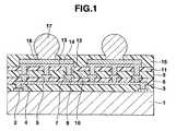
- FIG. 1shows a sectional view of a semiconductor device as a first embodiment of this invention.
- This semiconductor deviceincludes a silicon substrate (semiconductor substrate) 1.
- An integrated circuit (not shown) having a predetermined functionis provided in the center of an upper side of the silicon substrate 1, and a plurality of internal connection pads 2 made of a metal such as an aluminum-based metal are provided in peripheral parts of the upper surface in such a manner as to be electrically connected to the integrated circuit.
- a first insulating film 3 made of silicon oxide, silicon nitride or the likeis provided on the upper surfaces of the internal connection pads 2 and the silicon substrate 1.
- a plurality of openings 4are formed, for example, in matrix-form arrangement, in the first insulating film 3 in parts corresponding to the centers of the upper surfaces of the internal connection pads 2.
- An internal wiring line 5 of about 1 ⁇ m in thickness made of copper or a copper alloyis provided on an upper surface of the first insulating film 3 in such a manner as to be electrically connected to the internal connection pads 2 via the openings 4 of the first insulating film 3.
- the internal wiring line 5 shown in FIG. 1is an internal wiring line for grounding or for V DD (generically called “for power source"), and several to several ten internal wiring lines are provided in parallel and vertically spaced with each other to the surface of the drawing of FIG. 1 .
- internal wiring lines for control signals and for dataare omitted.
- a second insulating film 6 made of silicon oxide, silicon nitride or the likeis provided on the upper surfaces of the first insulating film 3 and the internal wiring lines 5. Openings 7 are formed in the second insulating film 6 in parts corresponding to a plurality (e.g., six) of connection pad portions of each of the internal wiring lines 5.
- Connection pads 8made of copper, a copper alloy or the like are provided in the openings 7 of the second insulating film 6 and on an upper surface of the second insulating film 6 in the vicinity or periphery of the openings 7 in such a manner as to be electrically connected to the connection pad portions of the internal wiring line 5.
- a third insulating film 9 made of silicon oxide, silicon nitride or the likeis provided on the upper surfaces of the second insulating film 6 and the connection pads 8. Openings 10 are formed in the third insulating film 9 in parts corresponding to the centers of upper surfaces of the connection pads 8.
- a protective film (insulating film) 11 made of a polyimide-based resin or the likeis provided on an upper surface of the third insulating film 9. Openings 12 are formed in the protective film 11 in parts corresponding to the openings 10 of the third insulating film 9. Foundation metal or lower layers 13 made of copper or the like are provided on an upper surface of the protective film 11. A wiring line or upper layer 14 made of copper is provided on an entire upper surface of the foundation metal layer 13. In this case, the thickness of the wiring line 14 is larger than the thickness of the internal wiring line 5, and is preferably 2 to 10 ⁇ m.
- Each of the foundation metal layers 13 and each of the wiring lines 14are connected to the plurality (e.g., three) of internal connection pads 2 via the plurality (e.g., three) of openings 12, 10 of the protective film 11 and the third insulating film 9.
- part of the foundation metal layer 13is only provided within the openings 10 formed in the third insulating film 9 and within the openings 12 formed in the protective film 11, but this is for figure convenience, and in practice, part of the wiring line 14 is also provided therein.
- each of the foundation metal layers 13 and each of the wiring lines 14are provided across the three respective openings 10 and 12, but this is also for figure convenience, and in practice, they are formed across several to several ten respective openings 10 and 12.
- the width of each of the wiring lines 14is decided in accordance with a later-described current from an external power source supplied to the solder balls.
- An overcoat film 15 made of a solder resist or the likeis provided on upper surfaces of the wiring lines 14 and the protective film 11.
- a substantially central part in longitudinal and width directions thereofserves as an external electrode pad portion, and openings 16 are formed in the overcoat film 15 in parts corresponding to the external electrode pad portions.
- a solder ball 17is provided within and above the opening 16 in such a manner as to be electrically connected to the external electrode pad portion of the wiring line 14.
- each of the internal wiring lines 5is electrically connected to the plurality of internal connection pads 2.
- connection pads 8are provided in each of the internal wiring lines 5.
- One wiring line 14is connected to several to several ten connection pads 8.
- Each of the solder balls 17is formed in one external electrode pad portion provided in each of the wiring lines 14.
- the number of solder balls 17 for grounding or for power sourcecorresponds to a few percent to several ten percent of the number of connection pads 8 for power source, so that the total number of solder balls 17 can be smaller than the total number of connection pads 8, thus making it possible to achieve a size reduction of the semiconductor device and an improvement of reliability in connection.
- a plurality of second wiring lines 14are arranged to extend in the longitudinal direction of the internal or first wiring lines 5, and if both lines 5 and 14 have the same width, no space is wasted in terms of layout, allowing a reduction in the size of the semiconductor device.
- Ni / To / Ti ⁇ No ⁇ Ni ⁇ To / Ti - 1be satisfied, wherein Ni is the number of openings 10 or 12 corresponding to one second wiring line, No is the number of external electrode pad portions provided in one second wiring line (or the number of openings 16), Ti is the thickness of the first wiring line 5, and To is the thickness of the second wiring line 14 including the foundation metal layer 13.
- FIG. 2shows a sectional view of a semiconductor device as a second embodiment of this invention.
- This semiconductor deviceis different from the semiconductor device shown in FIG. 1 in that a columnar electrode 18 made of copper is provided on an upper surface of an external electrode pad portion of a second wiring line 14, and a sealing film 19 made of an epoxy-based resin or the like is provided on an upper surface of a protective film 11 including the wiring line 14 so that an upper surface of the sealing film 19 may form one surface with upper surfaces of the columnar electrodes 18, and then a solder ball 17 is provided on the upper surface of the columnar electrode 18.
- first and second insulating films (interlayer insulating films) 3 and 6when so-called low-k is used as a material for first and second insulating films (interlayer insulating films) 3 and 6, the specific inductive capacity and elasticity modulus of the first and second insulating films 3 and 6 are in a trade-off relation. If the specific inductive capacity is reduced, a very fragile material having a young's elasticity modulus of 5 Gpa or less is used. In this case, in general, when the semiconductor device comprising the columnar electrodes 18 is mounted on a circuit board (not shown), cracks may be easily caused in the first and second insulating films 3 and 6 by stress due to a difference of thermal expansion coefficients between a silicon substrate 1 and the circuit board.
- the total number of solder balls 17can be smaller than the total number of connection pads 8 to increase the size of the solder balls 17, it is possible to reduce the stress due to the difference of thermal expansion coefficients between the silicon substrate 1 and the circuit board. Therefore, even if the so-called low-k which has a young's elasticity modulus of 5 Gpa or less and is thus very fragile is used as the material for first and second insulating films 3 and 6, it is possible to prevent the cracks from being easily caused in the first and second insulating films 3 and 6.
- one external electrode pad portionis provided in each of the second wiring lines 14 provided for several to several ten connection pads 8, but the number of external electrode pad portions provided in each of the wiring lines 14 is not necessarily limited to one, and a plurality of external electrode pad portions may be provided as long as the number thereof is smaller than the number of connection pads.
- One solder ball 17is formed under the wiring line 14.
- FIG. 3is a plan view of an external circuit board 20 to which the aforementioned semiconductor device is to be mounted face down.
- a power source wiring line pattern 22is provided on one surface of the circuit board 20.
- the power source wiring line pattern 22is a pattern which interconnects a plurality of feeder lines 21 arranged in parallel to correspond to the internal wiring lines 5, and each of the feeder lines 21 is provided with connection terminal portions 23 corresponding to the external electrode pad portions of the wiring line 14 of the semiconductor device.
- the solder balls 17 provided on the external electrode pad portionsare aligned with the connection terminal portions 23 of the circuit board 20 to mount the semiconductor device face down by bonding.
- the power source wiring line pattern 22 of the circuit board 20is desirably covered with a resist except for the connection terminal portions.
Landscapes
- Engineering & Computer Science (AREA)
- Microelectronics & Electronic Packaging (AREA)
- Computer Hardware Design (AREA)
- Power Engineering (AREA)
- Physics & Mathematics (AREA)
- Condensed Matter Physics & Semiconductors (AREA)
- General Physics & Mathematics (AREA)
- Geometry (AREA)
- Internal Circuitry In Semiconductor Integrated Circuit Devices (AREA)
Description
- This invention relates to a semiconductor device and a mounting structure thereof.
- Recently, in equipment such as personal computers and mobile devices, it has often been the case that, in order to reduce equipment size, a semiconductor device is flip-chip-mounted on a substrate. In this case, a method is employed, wherein a bare semiconductor substrate having an integrated circuit formed therein is directly provided with external electrode pads connected to the integrated circuit, and solder balls are formed on the external electrode pads, and then the solder balls are bonded to connection terminals of an external circuit board, thereby minimizing a mounting area (e.g., refer to Jpn. Pat. Appln.
KOKAI Publication No. 2001-196374 - In the above-mentioned semiconductor device, a silicon oxide film is formed on a silicon substrate, and a plurality of through-holes are formed in the silicon oxide film and metal layers are provided in the through-holes. Then, a thin silicon layer is formed on the silicon oxide film, and an integrated circuit including P-type and/or N-type MOS transistors is formed in the silicon layer, and then an upper surface of the integrated circuit is covered with an interlayer insulating film. Subsequently, the silicon substrate is polished in its thickness direction from its lower side so that it completely removed to expose a lower surface of the silicon oxide film. Then, external electrode pad portions are formed at places corresponding to the through-holes provided in the silicon oxide film before solder balls are provided on the external electrode pad portions. In this manner, the external electrode pad portions and the solder balls are provided to correspond to one another in the metal layers connected to the integrated circuit via the through-holes.
- Recently, semiconductor devices for control use driven at a high-speed clock of several gigahertz have emerged. It is necessary to supply a current of several tens of A from an external power source to such a semiconductor device. In this case, if the diameter of the solder balls provided on the external electrode pad portions is about 100 µm, a current of about 30 mA can only be passed to one solder ball in order to prevent the breakdown of the solder balls due to heat generation. Therefore, when a power source of a large current of several tens of A is required, a current passed to several thousand external electrode pad portions via several thousand solder balls converges inside.
- For the purpose of, for example, face-down mounting to connection terminal portions of the external circuit board via the solder balls thus provided on a large number of external electrode pad portions, the size of the semiconductor device is significantly increased, which requires a large mounting area. Moreover, due to the large number of solder balls, a short-circuit occurs in a bonding step, and there is a great variation in the size of the solder balls, making it impossible to obtain reliability in connection.
WO-A-2005/024912 discloses an interconnect structure with one or more thick metal layers under Controlled Collapse Chip Connection (C4) bumps at a die or wafer level, wherein each thick metal layer may be coupled to a row of C4 bumps.US-A-2004/0079966 discloses a chip structure comprising cross laminations of dielectric-multi layers and interconnected metal layers, which connects with external circuits through nodes for applying ground voltage or power voltage.- Therefore, this invention is directed to provide a semiconductor device and a mounting structure thereof in which the number of external electrode pad portions can be reduced to achieve a size reduction and an improvement of reliability in connection.
- In order to achieve the above object, this invention provides a semiconductor device according to appended
claim 1 and a mounting structure comprising the semiconductor device according to appendedclaim 16. - Other embodiments are defined by the dependent claims. According to this invention, the wiring line for external connection is connected to the internal wiring line through a plurality of openings formed in the second insulating film. Thus, the number of the wiring line may be decreased in comparison with the prior art, to allow the semiconductor device to become smaller and higher reliability in connection.
- Additional objects and advantages of the invention will be set forth in the description which follows, and in part will be obvious from the description, or may be learned by practice of the invention. The objects and advantages of the invention may be realized and obtained by means of the instrumentalities and combinations particularly pointed out hereinafter.
- The accompanying drawings, which are incorporated in and constitute a part of the specification, illustrate embodiments of the invention, and together with the general description given above and the detailed description of the embodiments given below, serve to explain the principles of the invention.
FIG. 1 is a sectional view of a semiconductor device as a first embodiment of this invention;FIG. 2 is a sectional view of a semiconductor device as a second embodiment of this invention; andFIG. 3 is a plan view showing one embodiment of a circuit board to which the semiconductor device of this invention is connected.FIG. 1 shows a sectional view of a semiconductor device as a first embodiment of this invention. This semiconductor device includes a silicon substrate (semiconductor substrate) 1. An integrated circuit (not shown) having a predetermined function is provided in the center of an upper side of thesilicon substrate 1, and a plurality ofinternal connection pads 2 made of a metal such as an aluminum-based metal are provided in peripheral parts of the upper surface in such a manner as to be electrically connected to the integrated circuit.- A first
insulating film 3 made of silicon oxide, silicon nitride or the like is provided on the upper surfaces of theinternal connection pads 2 and thesilicon substrate 1. A plurality ofopenings 4 are formed, for example, in matrix-form arrangement, in the firstinsulating film 3 in parts corresponding to the centers of the upper surfaces of theinternal connection pads 2. Aninternal wiring line 5 of about 1 µm in thickness made of copper or a copper alloy is provided on an upper surface of the firstinsulating film 3 in such a manner as to be electrically connected to theinternal connection pads 2 via theopenings 4 of the firstinsulating film 3. - Here, the
internal wiring line 5 shown inFIG. 1 is an internal wiring line for grounding or for VDD (generically called "for power source"), and several to several ten internal wiring lines are provided in parallel and vertically spaced with each other to the surface of the drawing ofFIG. 1 . InFIG. 1 , internal wiring lines for control signals and for data are omitted. - A second
insulating film 6 made of silicon oxide, silicon nitride or the like is provided on the upper surfaces of the firstinsulating film 3 and theinternal wiring lines 5.Openings 7 are formed in the secondinsulating film 6 in parts corresponding to a plurality (e.g., six) of connection pad portions of each of theinternal wiring lines 5. Connection pads 8 made of copper, a copper alloy or the like are provided in theopenings 7 of the secondinsulating film 6 and on an upper surface of the secondinsulating film 6 in the vicinity or periphery of theopenings 7 in such a manner as to be electrically connected to the connection pad portions of theinternal wiring line 5. A thirdinsulating film 9 made of silicon oxide, silicon nitride or the like is provided on the upper surfaces of the secondinsulating film 6 and theconnection pads 8.Openings 10 are formed in the thirdinsulating film 9 in parts corresponding to the centers of upper surfaces of theconnection pads 8.- A protective film (insulating film) 11 made of a polyimide-based resin or the like is provided on an upper surface of the third
insulating film 9.Openings 12 are formed in theprotective film 11 in parts corresponding to theopenings 10 of the thirdinsulating film 9. Foundation metal orlower layers 13 made of copper or the like are provided on an upper surface of theprotective film 11. A wiring line orupper layer 14 made of copper is provided on an entire upper surface of thefoundation metal layer 13. In this case, the thickness of thewiring line 14 is larger than the thickness of theinternal wiring line 5, and is preferably 2 to 10 µm. Each of thefoundation metal layers 13 and each of thewiring lines 14 are connected to the plurality (e.g., three) ofinternal connection pads 2 via the plurality (e.g., three) ofopenings protective film 11 and the thirdinsulating film 9. Here, inFIG. 1 , part of thefoundation metal layer 13 is only provided within theopenings 10 formed in the thirdinsulating film 9 and within theopenings 12 formed in theprotective film 11, but this is for figure convenience, and in practice, part of thewiring line 14 is also provided therein. Moreover, each of thefoundation metal layers 13 and each of thewiring lines 14 are provided across the threerespective openings respective openings wiring lines 14 is decided in accordance with a later-described current from an external power source supplied to the solder balls. - An
overcoat film 15 made of a solder resist or the like is provided on upper surfaces of thewiring lines 14 and theprotective film 11. In each of thewiring lines 14, a substantially central part in longitudinal and width directions thereof serves as an external electrode pad portion, andopenings 16 are formed in theovercoat film 15 in parts corresponding to the external electrode pad portions. Asolder ball 17 is provided within and above the opening 16 in such a manner as to be electrically connected to the external electrode pad portion of thewiring line 14. - As described above, in this semiconductor device, there are provided several to several ten
internal wiring lines 5, and each of them is electrically connected to the plurality ofinternal connection pads 2. There are provided a number ofconnection pads 8 in each of theinternal wiring lines 5. Onewiring line 14 is connected to several to several tenconnection pads 8. Each of thesolder balls 17 is formed in one external electrode pad portion provided in each of thewiring lines 14. - Therefore, in this semiconductor device, the number of
solder balls 17 for grounding or for power source corresponds to a few percent to several ten percent of the number ofconnection pads 8 for power source, so that the total number ofsolder balls 17 can be smaller than the total number ofconnection pads 8, thus making it possible to achieve a size reduction of the semiconductor device and an improvement of reliability in connection. - Here, a plurality of
second wiring lines 14 are arranged to extend in the longitudinal direction of the internal orfirst wiring lines 5, and if bothlines first wiring lines 5 and the wiringsecond lines 14 via the electrode pad portions are equal, it is recommended that
be satisfied, wherein Ni is the number ofopenings first wiring line 5, and To is the thickness of thesecond wiring line 14 including thefoundation metal layer 13. FIG. 2 shows a sectional view of a semiconductor device as a second embodiment of this invention. This semiconductor device is different from the semiconductor device shown inFIG. 1 in that acolumnar electrode 18 made of copper is provided on an upper surface of an external electrode pad portion of asecond wiring line 14, and a sealingfilm 19 made of an epoxy-based resin or the like is provided on an upper surface of aprotective film 11 including thewiring line 14 so that an upper surface of the sealingfilm 19 may form one surface with upper surfaces of thecolumnar electrodes 18, and then asolder ball 17 is provided on the upper surface of thecolumnar electrode 18.- In this semiconductor device, when so-called low-k is used as a material for first and second insulating films (interlayer insulating films) 3 and 6, the specific inductive capacity and elasticity modulus of the first and second insulating
films columnar electrodes 18 is mounted on a circuit board (not shown), cracks may be easily caused in the first and second insulatingfilms silicon substrate 1 and the circuit board. - However, in the second embodiment, since the total number of
solder balls 17 can be smaller than the total number ofconnection pads 8 to increase the size of thesolder balls 17, it is possible to reduce the stress due to the difference of thermal expansion coefficients between thesilicon substrate 1 and the circuit board. Therefore, even if the so-called low-k which has a young's elasticity modulus of 5 Gpa or less and is thus very fragile is used as the material for first and second insulatingfilms films - In the embodiments described above, one external electrode pad portion is provided in each of the
second wiring lines 14 provided for several to several tenconnection pads 8, but the number of external electrode pad portions provided in each of the wiring lines 14 is not necessarily limited to one, and a plurality of external electrode pad portions may be provided as long as the number thereof is smaller than the number of connection pads. Onesolder ball 17 is formed under thewiring line 14. FIG. 3 is a plan view of anexternal circuit board 20 to which the aforementioned semiconductor device is to be mounted face down. A power sourcewiring line pattern 22 is provided on one surface of thecircuit board 20. The power sourcewiring line pattern 22 is a pattern which interconnects a plurality offeeder lines 21 arranged in parallel to correspond to theinternal wiring lines 5, and each of thefeeder lines 21 is provided withconnection terminal portions 23 corresponding to the external electrode pad portions of thewiring line 14 of the semiconductor device. Thesolder balls 17 provided on the external electrode pad portions are aligned with theconnection terminal portions 23 of thecircuit board 20 to mount the semiconductor device face down by bonding. Although not shown in the figure, the power sourcewiring line pattern 22 of thecircuit board 20 is desirably covered with a resist except for the connection terminal portions.

Claims (16)
- A semiconductor device comprising:a semiconductor substrate (1) having an integrated circuit that includes a plurality of internal connection pads (2);a first insulating film (3) having a plurality of first openings (4) corresponding to the internal connection pads (2), respectively formed on the semiconductor substrate (1);at least one power source internal wiring line (5) formed on the first insulating film (3) and connected to the internal connection pads (2) via the first openings (4);a second insulating film (6) formed on the first insulating film (3) and on the internal wiring line (5) and having a plurality of second openings (7) exposing parts of the internal wiring line (5); andat least one wiring line (13, 14) formed on an upper side of the second insulating film (6) to correspond to the internal wiring line (5) and electrically connected to the internal wiring line (5) via the plurality of the second openings (7) of the second insulating film (6),
wherein said at least one wiring line (14) has at least one external electrode pad portion whose number is smaller than the number of the second openings (7) in the second insulating film (6),
characterized in that
the at least one wiring line (13, 14) has a thickness thicker than the internal wiring line (5) and a length shorter than the internal wiring line (5), and
the number of the second openings (7) of the second insulating film (6) is larger than the number of the first openings (4) of the first insulating film (3). - The semiconductor device according to claim 1, wherein a solder ball (17) is provided on the external electrode pad portion of said wiring line (14).
- The semiconductor device according to claim 1, wherein a columnar electrode (18) is provided on the external electrode pad portion of said wiring line (14).
- The semiconductor device according to claim 3, wherein a solder ball (17) is provided on the columnar electrode (18).
- The semiconductor device according to claim 1, which further comprises connection pads (8) provided in the second openings (7) of the second insulating film (6) covering an upper surface of the power source internal wiring line (5).
- The semiconductor device according to claim 5, wherein the second insulating film (6, 9) includes a first layer (6) formed between the connection pads (8), and a second layer (9) provided on the first layer (6) and both layers (6, 9) having first openings (10) formed at positions corresponding to the connection pads (8).
- The semiconductor device according to claim 1, wherein the second layer has a layer structure constituted of a plurality of layers (6, 9).
- The semiconductor device according to claim 1, wherein said wiring line (14) and the internal wiring line (5) are made of copper or a copper alloy.
- The semiconductor device according to claim 1, wherein the Young's elasticity modulus of at least one of the first (3) and second (6) insulating films is 5 Gpa or less.
- The semiconductor device according to claim 1, wherein said wiring line (14) and the internal wiring line (5) have the same width.
- The semiconductor device according to claim 1, wherein the plurality of said wiring lines (14) are arranged along the internal wiring line (5).
- The semiconductor device according to claim 1, wherein

is satisfied, where Ni is the number of the second openings (7) corresponding to said wiring line (14), No is the number of external electrode pad portions provided in said wiring line (14), Ti is the thickness of the internal wiring line (5), and To is the thickness of said wiring line (14). - The semiconductor device according to claim 1, wherein the first insulating film (3) is made of low-k.
- The semiconductor device according to claim 1, wherein the second insulating film (6) is made of low-k.
- The semiconductor device according to claim 13 or 14, wherein the device further includes a columnar electrode on said wiring line.
- A semiconductor device and a mounting structure therefore, comprising;
the semiconductor device according to any of claims 1 to 15, and
the mounting structure which includes:a substrate (20) having a power source pattern (22) with at least one power source terminal portion (23) corresponding to the external electrode pad portion of the semiconductor device; anda solder layer bonding the external electrode pad portion to the power source terminal portion (23) of the power source pattern (22).

Applications Claiming Priority (2)
| Application Number | Priority Date | Filing Date | Title |
|---|---|---|---|
| JP2005161026AJP4449824B2 (en) | 2005-06-01 | 2005-06-01 | Semiconductor device and its mounting structure |
| PCT/JP2006/311166WO2006129832A1 (en) | 2005-06-01 | 2006-05-30 | Semiconductor device and mounting structure thereof |
Publications (2)
| Publication Number | Publication Date |
|---|---|
| EP1897138A1 EP1897138A1 (en) | 2008-03-12 |
| EP1897138B1true EP1897138B1 (en) | 2010-03-03 |
Family
ID=36875893
Family Applications (1)
| Application Number | Title | Priority Date | Filing Date |
|---|---|---|---|
| EP06747146ANot-in-forceEP1897138B1 (en) | 2005-06-01 | 2006-05-30 | Semiconductor device and mounting structure thereof |
Country Status (7)
| Country | Link |
|---|---|
| US (1) | US7719116B2 (en) |
| EP (1) | EP1897138B1 (en) |
| JP (1) | JP4449824B2 (en) |
| KR (1) | KR100877018B1 (en) |
| CN (1) | CN100514627C (en) |
| DE (1) | DE602006012674D1 (en) |
| WO (1) | WO2006129832A1 (en) |
Families Citing this family (21)
| Publication number | Priority date | Publication date | Assignee | Title |
|---|---|---|---|---|
| US8552559B2 (en)* | 2004-07-29 | 2013-10-08 | Megica Corporation | Very thick metal interconnection scheme in IC chips |
| JP4449824B2 (en)* | 2005-06-01 | 2010-04-14 | カシオ計算機株式会社 | Semiconductor device and its mounting structure |
| JP4193897B2 (en)* | 2006-05-19 | 2008-12-10 | カシオ計算機株式会社 | Semiconductor device and manufacturing method thereof |
| US8022552B2 (en)* | 2006-06-27 | 2011-09-20 | Megica Corporation | Integrated circuit and method for fabricating the same |
| JP2008226945A (en)* | 2007-03-09 | 2008-09-25 | Casio Comput Co Ltd | Semiconductor device and manufacturing method thereof |
| US8193636B2 (en)* | 2007-03-13 | 2012-06-05 | Megica Corporation | Chip assembly with interconnection by metal bump |
| US7906424B2 (en) | 2007-08-01 | 2011-03-15 | Advanced Micro Devices, Inc. | Conductor bump method and apparatus |
| US20090032941A1 (en)* | 2007-08-01 | 2009-02-05 | Mclellan Neil | Under Bump Routing Layer Method and Apparatus |
| US20090079072A1 (en)* | 2007-09-21 | 2009-03-26 | Casio Computer Co., Ltd. | Semiconductor device having low dielectric insulating film and manufacturing method of the same |
| US8587124B2 (en) | 2007-09-21 | 2013-11-19 | Teramikros, Inc. | Semiconductor device having low dielectric insulating film and manufacturing method of the same |
| KR100910231B1 (en)* | 2007-11-30 | 2009-07-31 | 주식회사 하이닉스반도체 | Wafer level semiconductor package and method for manufacturing same |
| JP4666028B2 (en) | 2008-03-31 | 2011-04-06 | カシオ計算機株式会社 | Semiconductor device |
| US8314474B2 (en) | 2008-07-25 | 2012-11-20 | Ati Technologies Ulc | Under bump metallization for on-die capacitor |
| JP2010205941A (en)* | 2009-03-03 | 2010-09-16 | Panasonic Corp | Semiconductor chip, and semiconductor device |
| KR101169531B1 (en) | 2009-07-03 | 2012-07-27 | 가부시키가이샤 테라미크로스 | Semiconductor construct and manufacturing method thereof as well as semiconductor device and manufacturing method thereof |
| DE102009035437B4 (en)* | 2009-07-31 | 2012-09-27 | Globalfoundries Dresden Module One Llc & Co. Kg | A semiconductor device having a stress buffering material formed over a low ε metallization system |
| US8759209B2 (en)* | 2010-03-25 | 2014-06-24 | Stats Chippac, Ltd. | Semiconductor device and method of forming a dual UBM structure for lead free bump connections |
| JP5590985B2 (en)* | 2010-06-21 | 2014-09-17 | 新光電気工業株式会社 | Semiconductor device and manufacturing method thereof |
| KR102194719B1 (en)* | 2014-06-12 | 2020-12-23 | 삼성전기주식회사 | Package board and package using the same |
| CN110168707B (en)* | 2017-07-13 | 2023-08-29 | 富士电机株式会社 | Semiconductor device with a semiconductor device having a plurality of semiconductor chips |
| US12125811B2 (en)* | 2018-06-15 | 2024-10-22 | Texas Instruments Incorporated | Semiconductor structure and method for wafer scale chip package |
Family Cites Families (28)
| Publication number | Priority date | Publication date | Assignee | Title |
|---|---|---|---|---|
| US5486493A (en)* | 1994-02-25 | 1996-01-23 | Jeng; Shin-Puu | Planarized multi-level interconnect scheme with embedded low-dielectric constant insulators |
| JP3504421B2 (en)* | 1996-03-12 | 2004-03-08 | 株式会社ルネサステクノロジ | Semiconductor device |
| JPH11111860A (en)* | 1997-10-06 | 1999-04-23 | Mitsubishi Electric Corp | Semiconductor device |
| US6936531B2 (en)* | 1998-12-21 | 2005-08-30 | Megic Corporation | Process of fabricating a chip structure |
| JP3502800B2 (en)* | 1999-12-15 | 2004-03-02 | 新光電気工業株式会社 | Method for manufacturing semiconductor device |
| JP3395747B2 (en) | 2000-01-11 | 2003-04-14 | 日本電気株式会社 | Manufacturing method of semiconductor integrated circuit |
| JP2001196413A (en)* | 2000-01-12 | 2001-07-19 | Mitsubishi Electric Corp | Semiconductor device, method of manufacturing semiconductor device, CMP apparatus, and CMP method |
| US7372161B2 (en)* | 2000-10-18 | 2008-05-13 | Megica Corporation | Post passivation interconnection schemes on top of the IC chips |
| JP2002141436A (en) | 2000-11-01 | 2002-05-17 | Hitachi Ltd | Semiconductor device and manufacturing method thereof |
| JP3566203B2 (en)* | 2000-12-06 | 2004-09-15 | 株式会社東芝 | Semiconductor device and manufacturing method thereof |
| JP3561747B2 (en)* | 2001-03-30 | 2004-09-02 | ユーディナデバイス株式会社 | Multilayer wiring structure of high frequency semiconductor device |
| JP2002329976A (en)* | 2001-04-26 | 2002-11-15 | Kyocera Corp | Multilayer wiring board |
| JP2003031576A (en)* | 2001-07-17 | 2003-01-31 | Nec Corp | Semiconductor element and manufacturing method therefor |
| US6762505B2 (en)* | 2001-11-29 | 2004-07-13 | Sun Microsystems | 150 degree bump placement layout for an integrated circuit power grid |
| WO2004015771A2 (en)* | 2002-08-09 | 2004-02-19 | Casio Computer Co., Ltd. | Semiconductor device and method of manufacturing the same |
| US6717270B1 (en)* | 2003-04-09 | 2004-04-06 | Motorola, Inc. | Integrated circuit die I/O cells |
| WO2005024912A2 (en)* | 2003-09-09 | 2005-03-17 | Intel Corporation | Methods of processing thick ild layers using spray coating or lamination for c4 wafer level thick metal integrated flow |
| US6977435B2 (en)* | 2003-09-09 | 2005-12-20 | Intel Corporation | Thick metal layer integrated process flow to improve power delivery and mechanical buffering |
| JP2005093575A (en)* | 2003-09-16 | 2005-04-07 | Nec Electronics Corp | Semiconductor integrated circuit device and wiring layout method |
| TWI278048B (en)* | 2003-11-10 | 2007-04-01 | Casio Computer Co Ltd | Semiconductor device and its manufacturing method |
| JP4242336B2 (en)* | 2004-02-05 | 2009-03-25 | パナソニック株式会社 | Semiconductor device |
| US6888253B1 (en)* | 2004-03-11 | 2005-05-03 | Northrop Grumman Corporation | Inexpensive wafer level MMIC chip packaging |
| JP3925809B2 (en)* | 2004-03-31 | 2007-06-06 | カシオ計算機株式会社 | Semiconductor device and manufacturing method thereof |
| JP4449824B2 (en)* | 2005-06-01 | 2010-04-14 | カシオ計算機株式会社 | Semiconductor device and its mounting structure |
| JP4222400B2 (en)* | 2006-09-26 | 2009-02-12 | カシオ計算機株式会社 | Manufacturing method of semiconductor device |
| US8587124B2 (en)* | 2007-09-21 | 2013-11-19 | Teramikros, Inc. | Semiconductor device having low dielectric insulating film and manufacturing method of the same |
| JP4596001B2 (en)* | 2007-12-12 | 2010-12-08 | カシオ計算機株式会社 | Manufacturing method of semiconductor device |
| JP4666028B2 (en)* | 2008-03-31 | 2011-04-06 | カシオ計算機株式会社 | Semiconductor device |
- 2005
- 2005-06-01JPJP2005161026Apatent/JP4449824B2/ennot_activeExpired - Fee Related
- 2006
- 2006-05-30DEDE602006012674Tpatent/DE602006012674D1/enactiveActive
- 2006-05-30WOPCT/JP2006/311166patent/WO2006129832A1/enactiveApplication Filing
- 2006-05-30CNCNB2006800014794Apatent/CN100514627C/ennot_activeExpired - Fee Related
- 2006-05-30EPEP06747146Apatent/EP1897138B1/ennot_activeNot-in-force
- 2006-05-30KRKR1020077013201Apatent/KR100877018B1/ennot_activeExpired - Fee Related
- 2006-05-31USUS11/443,858patent/US7719116B2/ennot_activeExpired - Fee Related
Also Published As
| Publication number | Publication date |
|---|---|
| CN100514627C (en) | 2009-07-15 |
| KR100877018B1 (en) | 2009-01-07 |
| US20060273463A1 (en) | 2006-12-07 |
| CN101091250A (en) | 2007-12-19 |
| WO2006129832A1 (en) | 2006-12-07 |
| DE602006012674D1 (en) | 2010-04-15 |
| EP1897138A1 (en) | 2008-03-12 |
| JP2006339331A (en) | 2006-12-14 |
| JP4449824B2 (en) | 2010-04-14 |
| US7719116B2 (en) | 2010-05-18 |
| KR20070088688A (en) | 2007-08-29 |
Similar Documents
| Publication | Publication Date | Title |
|---|---|---|
| EP1897138B1 (en) | Semiconductor device and mounting structure thereof | |
| US7262513B2 (en) | Apparatus and method extending flip-chip pad structures for wirebonding on low-k dielectric silicon | |
| US7511376B2 (en) | Circuitry component with metal layer over die and extending to place not over die | |
| US7898058B2 (en) | Integrated chip package structure using organic substrate and method of manufacturing the same | |
| US9030029B2 (en) | Chip package with die and substrate | |
| US8835221B2 (en) | Integrated chip package structure using ceramic substrate and method of manufacturing the same | |
| US7242093B2 (en) | Semiconductor device | |
| US7323788B2 (en) | Semiconductor device and manufacturing method of them | |
| US6587353B2 (en) | Semiconductor device | |
| KR100983409B1 (en) | A semiconductor integrated circuit device | |
| JP4767556B2 (en) | Semiconductor device |
Legal Events
| Date | Code | Title | Description |
|---|---|---|---|
| PUAI | Public reference made under article 153(3) epc to a published international application that has entered the european phase | Free format text:ORIGINAL CODE: 0009012 | |
| 17P | Request for examination filed | Effective date:20070514 | |
| AK | Designated contracting states | Kind code of ref document:A1 Designated state(s):DE FR GB | |
| 17Q | First examination report despatched | Effective date:20080411 | |
| RBV | Designated contracting states (corrected) | Designated state(s):DE FR GB | |
| DAX | Request for extension of the european patent (deleted) | ||
| GRAP | Despatch of communication of intention to grant a patent | Free format text:ORIGINAL CODE: EPIDOSNIGR1 | |
| RTI1 | Title (correction) | Free format text:SEMICONDUCTOR DEVICE AND MOUNTING STRUCTURE THEREOF | |
| RIC1 | Information provided on ipc code assigned before grant | Ipc:H01L 23/528 20060101AFI20090827BHEP Ipc:H01L 23/31 20060101ALI20090827BHEP Ipc:H01L 23/485 20060101ALI20090827BHEP | |
| GRAS | Grant fee paid | Free format text:ORIGINAL CODE: EPIDOSNIGR3 | |
| GRAA | (expected) grant | Free format text:ORIGINAL CODE: 0009210 | |
| AK | Designated contracting states | Kind code of ref document:B1 Designated state(s):DE FR GB | |
| REG | Reference to a national code | Ref country code:GB Ref legal event code:FG4D | |
| REF | Corresponds to: | Ref document number:602006012674 Country of ref document:DE Date of ref document:20100415 Kind code of ref document:P | |
| PLBE | No opposition filed within time limit | Free format text:ORIGINAL CODE: 0009261 | |
| STAA | Information on the status of an ep patent application or granted ep patent | Free format text:STATUS: NO OPPOSITION FILED WITHIN TIME LIMIT | |
| 26N | No opposition filed | Effective date:20101206 | |
| REG | Reference to a national code | Ref country code:DE Ref legal event code:R082 Ref document number:602006012674 Country of ref document:DE Representative=s name:GRUENECKER, KINKELDEY, STOCKMAIR & SCHWANHAEUS, DE | |
| REG | Reference to a national code | Ref country code:DE Ref legal event code:R081 Ref document number:602006012674 Country of ref document:DE Owner name:TERAMIKROS, INC., JP Free format text:FORMER OWNER: CASIO COMPUTER CO., LTD., TOKIO/TOKYO, JP Effective date:20111228 Ref country code:DE Ref legal event code:R082 Ref document number:602006012674 Country of ref document:DE Representative=s name:GRUENECKER, KINKELDEY, STOCKMAIR & SCHWANHAEUS, DE Effective date:20111228 Ref country code:DE Ref legal event code:R081 Ref document number:602006012674 Country of ref document:DE Owner name:AOI ELECTRONICS CO., LTD., TAKAMATSU, JP Free format text:FORMER OWNER: CASIO COMPUTER CO., LTD., TOKIO/TOKYO, JP Effective date:20111228 Ref country code:DE Ref legal event code:R082 Ref document number:602006012674 Country of ref document:DE Representative=s name:GRUENECKER PATENT- UND RECHTSANWAELTE PARTG MB, DE Effective date:20111228 | |
| REG | Reference to a national code | Ref country code:GB Ref legal event code:732E Free format text:REGISTERED BETWEEN 20120315 AND 20120321 | |
| REG | Reference to a national code | Ref country code:FR Ref legal event code:PLFP Year of fee payment:10 | |
| PGFP | Annual fee paid to national office [announced via postgrant information from national office to epo] | Ref country code:GB Payment date:20150527 Year of fee payment:10 | |
| PGFP | Annual fee paid to national office [announced via postgrant information from national office to epo] | Ref country code:FR Payment date:20150508 Year of fee payment:10 | |
| PGFP | Annual fee paid to national office [announced via postgrant information from national office to epo] | Ref country code:DE Payment date:20160524 Year of fee payment:11 | |
| GBPC | Gb: european patent ceased through non-payment of renewal fee | Effective date:20160530 | |
| REG | Reference to a national code | Ref country code:DE Ref legal event code:R082 Ref document number:602006012674 Country of ref document:DE Representative=s name:GRUENECKER PATENT- UND RECHTSANWAELTE PARTG MB, DE Ref country code:DE Ref legal event code:R081 Ref document number:602006012674 Country of ref document:DE Owner name:AOI ELECTRONICS CO., LTD., TAKAMATSU, JP Free format text:FORMER OWNER: TERAMIKROS, INC., TOKYO, JP | |
| REG | Reference to a national code | Ref country code:FR Ref legal event code:ST Effective date:20170131 | |
| PG25 | Lapsed in a contracting state [announced via postgrant information from national office to epo] | Ref country code:FR Free format text:LAPSE BECAUSE OF NON-PAYMENT OF DUE FEES Effective date:20160531 | |
| PG25 | Lapsed in a contracting state [announced via postgrant information from national office to epo] | Ref country code:GB Free format text:LAPSE BECAUSE OF NON-PAYMENT OF DUE FEES Effective date:20160530 | |
| REG | Reference to a national code | Ref country code:DE Ref legal event code:R119 Ref document number:602006012674 Country of ref document:DE | |
| PG25 | Lapsed in a contracting state [announced via postgrant information from national office to epo] | Ref country code:DE Free format text:LAPSE BECAUSE OF NON-PAYMENT OF DUE FEES Effective date:20171201 |