EP1892764B1 - Light-emitting device having light-emitting diodes - Google Patents
Light-emitting device having light-emitting diodesDownload PDFInfo
- Publication number
- EP1892764B1 EP1892764B1EP07118916.1AEP07118916AEP1892764B1EP 1892764 B1EP1892764 B1EP 1892764B1EP 07118916 AEP07118916 AEP 07118916AEP 1892764 B1EP1892764 B1EP 1892764B1
- Authority
- EP
- European Patent Office
- Prior art keywords
- leds
- led
- light emitting
- electrode
- row
- Prior art date
- Legal status (The legal status is an assumption and is not a legal conclusion. Google has not performed a legal analysis and makes no representation as to the accuracy of the status listed.)
- Expired - Lifetime
Links
Images


Classifications
- H—ELECTRICITY
- H10—SEMICONDUCTOR DEVICES; ELECTRIC SOLID-STATE DEVICES NOT OTHERWISE PROVIDED FOR
- H10H—INORGANIC LIGHT-EMITTING SEMICONDUCTOR DEVICES HAVING POTENTIAL BARRIERS
- H10H29/00—Integrated devices, or assemblies of multiple devices, comprising at least one light-emitting semiconductor element covered by group H10H20/00
- H10H29/10—Integrated devices comprising at least one light-emitting semiconductor component covered by group H10H20/00
- H10H29/14—Integrated devices comprising at least one light-emitting semiconductor component covered by group H10H20/00 comprising multiple light-emitting semiconductor components
- H10H29/142—Two-dimensional arrangements, e.g. asymmetric LED layout
- H—ELECTRICITY
- H10—SEMICONDUCTOR DEVICES; ELECTRIC SOLID-STATE DEVICES NOT OTHERWISE PROVIDED FOR
- H10H—INORGANIC LIGHT-EMITTING SEMICONDUCTOR DEVICES HAVING POTENTIAL BARRIERS
- H10H20/00—Individual inorganic light-emitting semiconductor devices having potential barriers, e.g. light-emitting diodes [LED]
- H10H20/80—Constructional details
- H10H20/81—Bodies
- H10H20/813—Bodies having a plurality of light-emitting regions, e.g. multi-junction LEDs or light-emitting devices having photoluminescent regions within the bodies
- H—ELECTRICITY
- H10—SEMICONDUCTOR DEVICES; ELECTRIC SOLID-STATE DEVICES NOT OTHERWISE PROVIDED FOR
- H10H—INORGANIC LIGHT-EMITTING SEMICONDUCTOR DEVICES HAVING POTENTIAL BARRIERS
- H10H20/00—Individual inorganic light-emitting semiconductor devices having potential barriers, e.g. light-emitting diodes [LED]
- H10H20/80—Constructional details
- H10H20/81—Bodies
- H10H20/822—Materials of the light-emitting regions
- H10H20/824—Materials of the light-emitting regions comprising only Group III-V materials, e.g. GaP
- H10H20/825—Materials of the light-emitting regions comprising only Group III-V materials, e.g. GaP containing nitrogen, e.g. GaN
- H—ELECTRICITY
- H10—SEMICONDUCTOR DEVICES; ELECTRIC SOLID-STATE DEVICES NOT OTHERWISE PROVIDED FOR
- H10H—INORGANIC LIGHT-EMITTING SEMICONDUCTOR DEVICES HAVING POTENTIAL BARRIERS
- H10H20/00—Individual inorganic light-emitting semiconductor devices having potential barriers, e.g. light-emitting diodes [LED]
- H10H20/80—Constructional details
- H10H20/83—Electrodes
- H10H20/831—Electrodes characterised by their shape
- H—ELECTRICITY
- H10—SEMICONDUCTOR DEVICES; ELECTRIC SOLID-STATE DEVICES NOT OTHERWISE PROVIDED FOR
- H10H—INORGANIC LIGHT-EMITTING SEMICONDUCTOR DEVICES HAVING POTENTIAL BARRIERS
- H10H20/00—Individual inorganic light-emitting semiconductor devices having potential barriers, e.g. light-emitting diodes [LED]
- H10H20/80—Constructional details
- H10H20/83—Electrodes
- H10H20/832—Electrodes characterised by their material
- H10H20/833—Transparent materials
- H—ELECTRICITY
- H10—SEMICONDUCTOR DEVICES; ELECTRIC SOLID-STATE DEVICES NOT OTHERWISE PROVIDED FOR
- H10H—INORGANIC LIGHT-EMITTING SEMICONDUCTOR DEVICES HAVING POTENTIAL BARRIERS
- H10H20/00—Individual inorganic light-emitting semiconductor devices having potential barriers, e.g. light-emitting diodes [LED]
- H10H20/80—Constructional details
- H10H20/85—Packages
- H10H20/857—Interconnections, e.g. lead-frames, bond wires or solder balls
- H—ELECTRICITY
- H10—SEMICONDUCTOR DEVICES; ELECTRIC SOLID-STATE DEVICES NOT OTHERWISE PROVIDED FOR
- H10H—INORGANIC LIGHT-EMITTING SEMICONDUCTOR DEVICES HAVING POTENTIAL BARRIERS
- H10H29/00—Integrated devices, or assemblies of multiple devices, comprising at least one light-emitting semiconductor element covered by group H10H20/00
- H10H29/10—Integrated devices comprising at least one light-emitting semiconductor component covered by group H10H20/00
- H10H29/14—Integrated devices comprising at least one light-emitting semiconductor component covered by group H10H20/00 comprising multiple light-emitting semiconductor components
- H—ELECTRICITY
- H01—ELECTRIC ELEMENTS
- H01L—SEMICONDUCTOR DEVICES NOT COVERED BY CLASS H10
- H01L2224/00—Indexing scheme for arrangements for connecting or disconnecting semiconductor or solid-state bodies and methods related thereto as covered by H01L24/00
- H01L2224/01—Means for bonding being attached to, or being formed on, the surface to be connected, e.g. chip-to-package, die-attach, "first-level" interconnects; Manufacturing methods related thereto
- H01L2224/18—High density interconnect [HDI] connectors; Manufacturing methods related thereto
- H01L2224/23—Structure, shape, material or disposition of the high density interconnect connectors after the connecting process
- H01L2224/24—Structure, shape, material or disposition of the high density interconnect connectors after the connecting process of an individual high density interconnect connector
Definitions
- the present inventionrelates to a light emitting device in which a plurality of light emitting diodes are monolithically formed on a substrate.
- LEDlight emitting means
- typical usage conditionsare approximately 1 V to 4 V for the drive voltage and approximately 20 mA for the drive current.
- LEDsWith the recent development of short-wavelength LEDs which uses a GaN-based compound semiconductor and commercialization of solid light sources of full color, white color, etc., application of LEDs for illumination purposes has been considered.
- an LEDis used for illumination, there may be cases in which the LED is used under conditions other than the above-described conditions of 1 V - 4 V of drive voltage and 20 mA of drive current.
- stepshave been taken to enable a larger current to flow through the LED and to increase the light emission output. In order to flow a larger current, an area of a pn junction of the LEDmust be increased so that the current density is reduced.
- Document JP 2001307506 Adescribes a GaN-based light emitting device comprises a plurality of light-emitting diodes that are grouped in two groups, whereby in each group two straight lines of diodes are connected in parallel, and the two groups are connected in anti-parallel.
- JP 2001156331 AJP 2000068555 A
- WO 0147039 A1light-emitting devices consisting of a plurality of light-emitting elements are presented, the elements being connected in series.
- JP 10107316 AAnother example is disclosed in JP 10107316 A , where a plurality of light-emitting diodes on a chip are connected in series or in parallel, or in series and parallel at a time.
- JP 2001 307506 AAnother light emitting device of relevant prior art is furthermore disclosed in JP 2001 307506 A .
- JP2000101136discloses a device comprising a plurality of light emitting diodes each of which has a p-n junction.
- the light emitting diodesare all connected in parallel, and diodes 10a1, 10a2, to 10an and 10b1, 10b2 to 10bn are connected mutually anti-parallel with respect to the polarity.
- US6060727discloses a light emitting semiconductor device comprising a common substrate having a support surface, and a plurality of laminate structures formed at different regions on the support surface of the common substrate.
- Each of the laminate structureshas at least one N-type layer, a light emitting layer and at least one P-type layer.
- the light emitting layeremits light at least perpendicularly to the support surface of the substrate.
- the laminate structures at the different regionsare made to emit light of a different wavelength.
- a light emitting devicewherein a plurality of GaN-based light emitting diodes are formed on an insulating substrate and the plurality of light emitting diodes are monolithically formed and connected in series.
- the plurality of light emitting diodesare arranged on the substrate in a two-dimensional pattern.
- the plurality of light emitting diodesare grouped into two groups and the two groups are connected between two electrodes in parallel so that the two groups are of opposite polarities.
- the plurality of light emitting diodesare connected by air bridge lines.
- the plurality of light emitting diodesare electrically separated by sapphire which is used as the substrate.
- the plurality of light emitting diodesare grouped into two groups having equal numbers of light emitting diodes, and the two groups of light emitting diode arrays are connected between two electrodes in parallel so that they are of apposite polarities.
- the light emitting diodes and the electrodeshave a planar shape of triangle.
- the overall shape of the plurality of light emitting diodes and the electrodesis approximate square.
- the electrodeis an electrode for an alternate current power supply.
- the two groups of light emitting diode arrayshave a common n electrode.
- a plurality of light emitting diodesare monolithically formed, that is, formed on a same substrate, and are connected in series. With this structure, the present invention allows a high drive voltage. By connecting a plurality of light emitting diodes along one direction, a DC drive is possible. By grouping the plurality of light emitting diodes into two groups and connecting the two groups between electrodes such that the two groups of light emitting diodes (light emitting diode arrays) are of opposite polarities from each other, it is possible to also allow an AC drive.
- the shapes of the light emitting diodes and the electrodesis a triangle, for the light emitting diodes and the electrodes, to form an approximate square shape as an overall shape by combining the triangles, and, as a consequence, it is possible to use a standard mounting structure in a similar manner.
- Fig. 1shows a basic structure of an LED 1 which is a GaN-based compound semiconductor light emitting diode.
- the LED 1has a structure in which a GaN layer 12, an Si-doped n-type GaN layer 14, an InGaN light emitting layer 16, an AlGaN layer 18, and a p-type GaN layer 20 are sequentially layered on a substrate 10, a p electrode 22 is formed in contact with the p-type GaN layer 20, and an n electrode 24 is formed in contact with the n-type GaN layer 14.
- the LED shown in Fig. 1is manufactured through the following process. First, a sapphire c-plane substrate is thermally treated for 10 minutes in a hydrogen atmosphere at a temperature of 1100 °C in an MOCVD device. Then, the temperature is reduced to 500 °C and silane gas and ammonia gas are supplied for 100 seconds to form a discontinuous SiN film on the substrate 10. This process is applied in order to reduce a dislocation density within the device and the SiN film is not shown in Fig. 1 . Next, trimethyl gallium and ammonia gas are supplied at the same temperature to grow a GaN layer to a thickness of 20 nm.
- the temperatureis raised to 1050 °C and trimethyl gallium and ammonia gas are supplied again to grow an undoped GaN (u-GaN) layer 12 and an Si-doped n-type GaN layer 14 to a thickness of 2 ⁇ m each. Then, the temperature is reduced to approximately 700 °C and an InGaN light emitting layer 16 is grown to a thickness of 2 nm.
- the temperatureis raised to 1000 °C, an AlGaN hole injection layer 18 is grown, and a p-type GaN layer 20 is grown.
- the waferis taken out of the MOCVD device and a Ni layer of 10 nm and a Au layer of 10 nm are sequentially vacuum-evaporated to form these layers on the surface of the grown layer.
- a thermal treatmentis applied in a nitrogen gas atmosphere containing 5% oxygen at a temperature of 520 °C so that the metal filmbecomes a p-type transparent electrode 22.
- a photoresistis applied over the entire surface and an etching process is applied for forming an n-type electrode using the photoresist as a mask.
- the depth of etchingis, for example, approximately 600 nm.
- a Ti layer of 5 nm thickness and an Al layer of 5 nm thicknessare formed above the n-type GaN layer 14 exposed by the etching process and a thermal treatment is applied in a nitrogen gas atmosphere at a temperature of 450 °C for 30 minutes to form an n-type electrode 24. Finally, a rearside of the substrate 10 is ground to a thickness of 100 ⁇ m and chips are cut away and mounted to obtain the LED 1.
- one GaN-based LED 1is formed on a substrate 1, but in the present invention, a plurality of LEDs 1 are monolithically formed on the substrate 10 in a two-dimensional array and the LEDs are connected to form the light emitting device (chip).
- “monolithic”indicates that all elements are formed on one single substrate.
- Fig. 2is a diagram showing an equivalent circuit of the light emitting device.
- the light emitting diodes formed in the two-dimensional arrayare grouped into two groups of same number of light emitting diodes (in Fig. 2 , 4 light emitting diodes).
- the LEDs 1 in each groupare connected in series and the two groups of LED arrays are connected in parallel between electrodes (drive electrodes) such that the two groups are of opposite polarities. In this manner, by connecting the array of LEDs in series, it is possible to drive the LEDs 1 at a high voltage in which the drive voltage of each LED is added.
- the LED arraysare connected in parallel between the electrodes such that the LED arrays are of opposite polarities, even when an AC power supply is used as a power supply, one of the LED array always emits light in each period of the power supply, which allows an effective light emission.
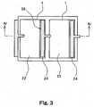
- Fig. 3is a partial plan view of an example not forming part of the present invention of a plurality of LEDs monolithically formed on the substrate 10.
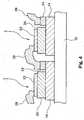
- Fig. 4is a diagram showing a IV-IV cross section of Fig. 3 .
- a p electrode 22 and an n electrode 24are formed on the upper surface of the LED 1 as shown in Fig. 1 .
- the p electrode 22 and the n electrode 24 of adjacent LEDs 1are connected through an air bridge line 28 and a plurality of LEDs 1 are connected in series.
- the LEDs 1are shown in a simple manner for explanation purposes. Specifically, only the n-GaN layer 14, the p-GaN layer 20, the p-electrode 22, and the n-electrode 24 are shown. In real applications, the InGaN light emitting layer 16 is also present as shown in Fig. 1 .
- the air bridge line 28connects from the p electrode 22 to the n electrode 24 through the air.
- the LEDs 1must be independent and electrically insulated from each other.
- the LEDs 1are separated on the sapphire substrate 10. Because sapphire is an insulating material, it is possible to electrically separate the LEDs 1. By using the sapphire substrate 10 as a resistive body for achieving an electrical separation between the LEDs, it is possible to electrically separate the LEDs in an easy and reliable manner.
- the light emitting elementit is also possible to employ an MIS in place of the LED having a pn junction.
- Fig. 5is a diagram showing another equivalent circuit of the light emitting device.
- 20 LEDs 1are connected in series to form one LED array and two such LED arrays (a total of 40 LEDs) are connected to a power supply in parallel.
- the drive voltage of the LED 1is set to 5 V, and thus, the drive voltage of each LED array is 100 V.
- the two LED arraysare connected in parallel to the power supply such that the LED arrays are of opposite polarities, similar to Fig. 2 . Light is always emitted from one of the LED arrays, regardless of the polarity of the power supply.
- Fig. 6shows an example not forming part of the present invention of a two-dimensional array and corresponds to the equivalent circuit diagram of Fig. 2 .
- a total of 40 LEDs 1are formed on the sapphire substrate 10 which are grouped into two groups of 20 LEDs 1.
- the groups of LEDs 1are connected in series by the air bridges 28 to form two LED arrays. More specifically, all of the LEDs 1 has a square shape of the same size and same shape.
- a first LED arraycomprises, from the top line toward the bottom line, a line of 6 LEDs are arranged in a straight line, a line of 7 LEDs are arranged in a straight line, and a line of 7 LEDs are arranged in a straight line.
- the first row (6 LEDs) and the second row (7 LEDs)are formed facing opposite directions and the second row and the third row are formed facing opposite directions.
- the first row and the second roware separated from each other and the second row and the third row are separated from each other, because rows of the other LED array are alternately inserted, as will be described later.
- the rightmost LED 1 of the first row and the rightmost LED 1 of the second roware connected by an air bridge line 28 and the leftnost LED 1 of the second row and the leftmost LED 1 of the third row are connected by an air bridge line 28 to construct a zigzag arrangement.
- the leftmost LED 1 of the first rowis connected to an electrode (pad) 32 formed on an upper left section of the substrate 10 by an air bridge line 28 and the rightmost LED 1 of the third row is connected to an electrode (pad) 32 formed on a lower right section of the substrate 10 by an air bridge line 28.
- the two electrodes (pads) 32have the same square shape as the LEDs 1.
- the second LED arrayis alternately formed in the spaces of the first LED array.
- the second LED array7 LEDs, 7 LEDs, and 6 LEDs are formed on straight lines from the top to the bottom, the first row is formed between the first row and the second row of the first LED array, the second row is formed between the second row and the third row of the first LED array, and the third row is formed below the third row of the first LED array.
- the first row and the second row of the second LED arrayare formed facing opposite directions and the second row and the third row of the second LED array are formed facing opposite directions.
- the rightmost LED 1 of the first rowis connected to the rightmost LED 1 of the second row by an air bridge line 28 and the leftmost LED 1 of the second row is connected to the leftmost LED of the third row by an air bridge line 28 to construct a zigzag arrangement.
- the leftmost LED of the first row of the second LED arrayis connected to the electrode 32 formed on the upper left section of the substrate 10 by an air bridge line 28 and the rightmost LED 1 of the third row is connected to the electrode 32 formed on the lower right section of the substrate 10 by an air bridge line 28.
- Polarities of the LED arrays with respect to the electrodes 32are opposite from each other.
- the overall shape of the light emitting device (chip)is rectangular. It should also be noted that two.electrodes 32 to which a power supply is supplied are formed in diagonally opposite positions of the rectangle and are spaced apart.
- Fig. 7is a circuit diagram of the circuit shown in Fig. 6 . It can be seen from this figure that each LED array is connected in series while bending in a zigzag pattern and two LED arrays have the zigzag shaped rows formed between the rows of the other LED array. By employing such a configuration, many LEDs 1 can be arranged on a small substrate 10. In addition, because only two electrodes 32 are required for 40 LEDs 1, the usage efficiency on the substrate 10 can be further improved. Moreover, when the LEDs 1 are individually formed in order to separate LEDs 1, the wafer must be cut for separation, but, in the present embodiment, the separation between LEDs 1 can be achieved through etching, which allows for narrowing of a gap between the LEDs 1.
- the separation between LEDs 1is achieved by etching and removing regions other than the LEDs 1 to the point which reaches the substrate 10 by using photoresist, reactive ion etching, and wet etching. Because the LED arrays alternately emit light, the light emission efficiency can be improved and heat discharging characteristic can also be improved. Moreover, by changing the number of LEDs 1 to be connected in series, the overall drive voltage can also be changed. In addition, by reducing the area of the LED 1, it is possible to increase the drive voltage per LED. When 20 LEDs 1 are serially connected and are driven with a commercially available power supply (100 V, 60 Hz), a light emission power of approximately 150 mW can be obtained. The drive current in this case is approximately 20 mA.
- a crossing section 34inevitably occurs in the air bridge line 28.
- this portioncrosses the line portion for connecting the first row and the second row of the first LED array.
- the air bridge line 28 of the present embodimentis not adhered to the substrate 10 as described above and extends through the air, distanced from the substrate 10. Because of this structure, short-circuiting due to contact of the air bridge lines 28 at the crossing section can be easily avoided. This is one advantage of using the air bridge line 28.
- the air bridge line 28is formed, for example, through the following processes.
- a photoresistis applied over the entire surface to a thickness of 2 ⁇ m and a post bake process is applied after a hole is opened in a shape of the air bridge line.
- a Ti layer of 10 nm and a Au layer of 10 nmare evaporated in this order through vacuum evaporation.
- a photoresistis again applied over the entire surface to a thickness of 2 ⁇ m and holes are opened in portions in which the air bridge lines are to be formed.
- using Ti and Au as electrodesAu is deposited over the entire surface of the electrodes to a thickness of 3 - 5 ⁇ m through ion plating (plating) in an electrolyte.
- the sampleis immersed in acetone, the photoresist is dissolved and removed through ultrasonic cleaning, and the air bridge line 28 is completed.
- the two-dimensional array patternpreferably satisfies the following conditions:
- Fig. 8shows an example not forming part of the present invention of a two-dimensional arrangement of a total of 6 LEDs 1 and Fig. 9 shows a circuit diagram of this configuration.
- the arrangement of Fig. 8is basically identical to that of Fig. 6.
- 6 LEDsare grouped into two groups of the same number to form LED arrays having 3 LEDs connected in series.
- the first LED arrayis arranged in a zigzag pattern with the first row having one LED and the second row having two LEDs.
- the LED of the first row and the rightmost LED 1 of the second roware connected in series by an air bridge line 28 and the two LEDs 1 of the second row are connected in series by an air bridge line 28.
- Electrodes (pads) 32are formed at an upper left section and a lower left section of the substrate 10.
- the LED 1 of the first rowis connected to the electrode 32 at the upper left section by an air bridge line and the leftmost LED 1 of the second row is connected to the electrode 32 at the lower left section.
- the second LED arrayis also arranged in a zigzag pattern and has two LEDs 1 on the first row and one LED 1 on the second row.
- the first row of the second LED arrayis formed between the first row and the second row of the first LED array and the second row of the second LED array is formed below the second row of the first LED array.
- the rightmost LED 1 of the first rowis connected in series to the LED 1 of the second row by an air bridge line 28 and the two LEDs 1 on the first row are connected in series by an air bridge line 28.
- the leftmost LED 1 of the first rowis connected to the electrode 32 at the upper left section by an air bridge line 28 and the LED 1 of the second row is connected to the electrode 32 at the lower left section by an air bridge line 28.
- two LED arraysare connected between the electrodes 32 in parallel such that they are of opposite polarities. Therefore, when an AC power supply is supplied, the two LED arrays alternately emit light.
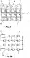
- Fig. 10shows an example not forming part of the present invention of a configuration in which a total of 14 LEDs are arranged in a two-dimensional pattern and Fig. 11 shows a circuit diagram of this configuration.
- 14 LEDsare grouped into two groups and the LED array has 7 LEDs connected in series.
- a first LED arrayis arranged in a zigzag pattern with the first row having 3 LEDs 1 and the second row having 4 LEDs 1.
- the leftmost LED of the first row and the leftmost LED 1 of the second roware connected in series by an air bridge line 28, 3 LEDs of the first row are connected in series by air bridge lines 28, and 4 LEDs 1 of the second row are connected in series by air bridge lines 28.
- Electrodes (pads) 32are formed at an upper right section and a lower right section of the substrate 10, the rightmost LED 1 of the first row is connected to the electrode 32 at the upper right section by an air bridge line and the rightmost LED 1 of the second row is connected to the electrode 32 at the lower right section.
- a second LED arrayalso is arranged in a zigzag pattern with a first row having 4 LEDs 1 and a second row having 3 LEDs 1. The first row of the second LED array is formed between the first row and the second row of the first LED array and the second row of the second LED array is formed below the second row of the first LED array.
- the leftmost LED 1 of the first rowis connected in series to the leftmost LED 1 of the second row by an air bridge line 28.
- LEDs 1 on the first roware connected in series and 3 LEDs 1 on the second row are connected in series.
- the rightmost LED 1 on the first rowis connected to the electrode 32 on the upper right section by an air bridge line 28 and the rightmost LED 1 on the second row is connected to the electrode 32 at the lower right section by an air bridge line 28.
- the two LED arraysare connected between the electrodes 32 in parallel such that they are of opposite polarities. Therefore, when an AC power supply is supplied, the two LED arrays alternately emit light.
- Characteristics common to the two-dimensional patterns of Figs. 6 , 8 , and 10are that the LEDs 1 have the same shape of approximate square and same size, the two electrodes (pads) also have approximate square shape and are not formed adjacent to each other (are formed separate from each other), the configuration is a combination of two LED arrays, the two LED arrays are bent and cross each other on the chip, the two LED arrays are connected between electrodes such that they are of opposite polarities, etc.
- Fig. 12shows a first embodiment of the present invention in which LEDs having a planar shape of triangle are arranged in a two-dimensional pattern and Fig. 13 shows a circuit diagram of this configuration.
- a total of 6 LEDs, LEDs 1a, 1b, 1c, 1d, 1e, and 1fare formed such that they have a planar shape of a triangle.
- LEDs 1a and 1 eare arranged opposing each other at one side of the triangle so that the two LEDs form an approximate square and LEDs 1b and 1f are placed opposing each other, so that the two LEDs form an approximate square.
- the LED 1d and an electrode 32 oppose andare connected to each other and the LED 1c and an electrode 32 oppose and are connected to each other.
- the two electrodes 32also have a planar shape of a triangle and are placed to form an approximate square.
- the opposing sides of the LEDsform an n electrode 24, that is, two opposing LEDs share the n electrode 24.
- the LED and the electrode 32are connected through the n electrode.
- the 6 LEDsare grouped into two groups similar to the above-described arrangements.
- a first LED arrayincludes the LEDs 1a, 1b, and 1c.
- a p electrode 22 of the LED 1ais connected to the electrode 32 by an air bridge line 28 and an n electrode 24 of the LED 1a is connected to a p electrode 22 of the LED 1b by an air bridge line 28.
- An n electrode 24 of the LED 1bis connected to a p electrode 22 of the LED 1c by an air bridge line 28.
- An n electrode 24 of the LED 1cis connected to the electrode 32.
- a second LED arrayincludes LEDs 1d, 1e, and 1f.
- the electrode 32is connected to a p electrode 22 of the LED 1f by an air bridge line 28
- an n electrode 24 of the LED 1fis connected to a p electrode 22 of the LED 1e by an air bridge line
- an n electrode 24 of the LED 1eis connected to a p electrode 22 of the LED 1d by an air bridge line 28
- an n electrode 24 of the LED 1dis connected to the electrode 32.
- the n electrode of the LED 1a which is a part of the first LED arrayis connected to the n electrode of the LED 1e which is a part of the second LED array and the n electrode of the LED 1b which is a part of the first LED array is connected to the n electrode of the LED 1f which is a part of the second LED array.
- the two LED arraysare connected between the electrodes 32 in parallel such that they are of opposite polarities.
- the LEDshave the same shape and the same size, and by placing the LEDs to oppose at one side and forming the electrode 32 in a triangular shape, it is possible to densely form the LEDs and electrodes to reduce the necessary area of the substrate.
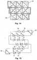
- Fig. 14shows another embodiment of the present invention in which LEDs having a planar shape of a triangle are arranged in a two-dimensional pattern and Fig. 15 shows a circuit diagram of this configuration.
- a total of 16 LEDsLEDs 1a - 1r are two-dimensionally formed.
- An n electrode 24is formed common to the LEDs at the opposing side.
- the LED 1 i and an electrode 32oppose each other and the LED 1h and an electrode 32 oppose each other.
- a first LED arrayincludes the LEDs 1a, 1b, 1c, 1d, 1e, 1f, 1g, and 1h and a second LED array includes the LEDs 1r, 1q, 1p, 1n, 1m, 1k, 1j, and 1i.
- An n electrode 24 of the LED 1bis connected to a p electrode 22 of the LED 1 c by an air bridge line 28 and an n electrode 24 of the LED 1e is connected to a p electrode 22 of the LED 1f by an air bridge line 28.
- An n electrode 24 of the LED 1qis connected to a p electrode 22 of the LED 1p by an air bridge line 28 and an n electrode of the LED 1m is connected to a p electrode 22 of the LED 1k by an air bridge line 28.
- Fig. 14also, a crossing portion occurs similar to Fig. 12 , but short-circuiting can be avoided by the air bridge lines 28.
- some of the n electrodes 24 in the two LED arraysare formed as common structures in order to reduce the amount of necessary wirings.
- the two LED arraysare connected between the electrodes 32 in parallel so that they are of opposite polarities and the device can be AC driven.
- Fig. 12shows a case of 6 LEDs
- Fig. 14shows a case of 16 LEDs. Similar two-dimensional arrangements can be achieved also with different numbers of LEDs.
- the present inventorshave created a light emitting device in which 38 LEDs are arranged in a two-dimensional pattern.
- the structurecan also be DC driven.
- the LED arraysare not connected between the electrodes to have opposite polarities, but rather, the LED array is connected in a forward direction along the direction of polarity of the DC power supply. By connecting a plurality of LEDs in series, it is possible to achieve a high voltage drive. Configurations for DC drive will now described.
- Fig. 16shows an example not forming part of the present invention in which two LEDs are connected in series and Fig. 17 shows a circuit diagram of this configuration.
- Each LED 1has a planar shape of a rectangle and an air bridge line 28 connects between two LEDs.
- An electrode 32is formed near each LED 1 and the electrode 32 and the LED 1 form a rectangular region. In other words, the electrode 32 occupies a portion of the rectangular region and the LED 1 is formed in the other portion in the rectangular region.
- Fig. 18shows an example not forming part of the present invention in which 4 LEDs are arranged in a two-dimensional pattern and Fig. 19 shows a circuit diagram of this configuration.
- each of the LEDs 1 of Fig. 16is divided into two LEDS and the two LEDs are connected in parallel.
- This configurationcan also be described as two LED arrays each of which is made of two LEDs connected in parallel in the forward direction.
- the LEDs 1a and 1bform one LED array and the LEDs 1c and 1d form another LED array.
- the LEDs 1a and 1cshare a p electrode 22 and an n electrode 24 and LEDs 1b and 1d also share a p electrode 22 and an n electrode 24.
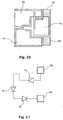
- Fig. 20shows an example not forming part of the present invention in which three LEDs are arranged in a two-dimensional pattern and Fig. 21 shows a circuit diagram of this configuration.
- LEDs 1a, 1b, and 1cdo not have the same shape and an electrode 32 is formed in a portion of the LED 1a.
- An n electrode 24 of the LED 1ais connected to a p electrode of the LED 1b by an air bridge line 28 striding over the LED 1b.
- Fig. 22shows an example not forming part of the present invention in which a total of 6 LEDs are arranged in a two-dimensional pattern and Fig. 23 shows a circuit diagram of this configuration.
- the LEDs 1a - 1fhave the same shape and same size and are connected in series.
- the LEDs 1a - 1care placed on a straight line and the LEDs 1d - 1f are placed on another straight line.
- the LEDs 1c and 1dare connected by an air bridge line 28.
- the overall shape of the chipcan be made approximate square.
- Fig. 24shows an example not forming part of the present invention in which a total of 5 LEDs are arranged in a two-dimensional pattern and Fig. 25 shows a circuit diagram of this configuration.
- LEDs 1 a - 1ehave the same shape (rectangle) and the same size. In this configuration also, the overall shape can be made approximate square.
- Figs. 26-31exemplify some alternative configurations not forming part of the present invention.
- Fig. 26shows a two-dimensional arrangement in an example not forming part of the present invention employing AC drive of a total of 40 LEDs.
- Fig. 27is a circuit diagram of this configuration.
- the configuration of Fig. 26differs from that of Fig. 6 in that some of the two groups of LED arrays share the n electrode 24 (refer to Fig. 5 ).
- an n electrode 24 of a second LED from the right of the first row of the first LED array(shown in the figure by ⁇ ) is shared as the n electrode 24 of the rightmost LED of the first row of the second LED array (shown in the figure by ⁇ ).
- Air bridge lines 28 at the ends of the LED arraysare commonly formed without crossing.
- Fig. 28shows a two-dimensional arrangement of an example not forming part of the present invention employing AC drive and a total of 14 LEDs.
- Fig. 29is a circuit diagram of this configuration.
- the configuration of Fig. 28differs from that of Fig. 10 in that some of the two groups of LED arrays share the n electrode 24.
- an n electrode 24 of the leftmost LED on a first row of a first LED array(shown in the figure by ⁇ ) is shared as an n electrode 24 of an LED located second from the right on a first row of a second LED array (shown in the figure by ⁇ ).
- Air bridge lines 28 at the endsare commonly formed.
- Fig. 30shows a two-dimensional arrangement of an example not forming part of the present invention employing AC drive and a total of 6 LEDs.
- Fig. 31is a circuit diagram of this configuration. In this configuration also, air bridge lines 28 at the ends ( ⁇ portion) are commonly formed. It can be considered that in this configuration also, an n electrode 24 in the first LED array and an n electrode 24 of the second LED array are shared.
Landscapes
- Led Devices (AREA)
- Led Device Packages (AREA)
- Illuminated Signs And Luminous Advertising (AREA)
- Electroluminescent Light Sources (AREA)
Abstract
Description
- The present invention relates to a light emitting device in which a plurality of light emitting diodes are monolithically formed on a substrate.
- When light emitting means such as a light emitting diode (LED) is used for display or the like, typical usage conditions are approximately 1 V to 4 V for the drive voltage and approximately 20 mA for the drive current. With the recent development of short-wavelength LEDs which uses a GaN-based compound semiconductor and commercialization of solid light sources of full color, white color, etc., application of LEDs for illumination purposes has been considered. When an LED is used for illumination, there may be cases in which the LED is used under conditions other than the above-described conditions of 1 V - 4 V of drive voltage and 20 mA of drive current. As a result, steps have been taken to enable a larger current to flow through the LED and to increase the light emission output. In order to flow a larger current, an area of a pn junction of the LEDmust be increased so that the current density is reduced.
- When the LED is used as a light source for illumination, it is convenient to use an AC power supply and allow use with a drive voltage of 100 V or greater. In addition, if the same light emission output is to be obtained with supply of the same power, the power loss can be reduced by applying a high voltage while maintaining a low current value. In the LEDs of the related art, however, it is not always possible to sufficiently increase the drive voltage. Some examples of the prior will now be cited. Document
JP 2001307506 A JP 2001156331 A JP 2000068555 A WO 0147039 A1 JP 10107316 A - Another light emitting device of relevant prior art is furthermore disclosed in
JP 2001 307506 A JP2000101136 US6060727 discloses a light emitting semiconductor device comprising a common substrate having a support surface, and a plurality of laminate structures formed at different regions on the support surface of the common substrate. Each of the laminate structures has at least one N-type layer, a light emitting layer and at least one P-type layer. The light emitting layer emits light at least perpendicularly to the support surface of the substrate. The laminate structures at the different regions are made to emit light of a different wavelength.- It is the object of the present invention to provide a light emitting device which can be operated with a high drive voltage and which has a small overall size.
- This object is achieved by a light emitting device according to
claim 1. - According to the present invention, there is provided a light emitting device wherein a plurality of GaN-based light emitting diodes are formed on an insulating substrate and the plurality of light emitting diodes are monolithically formed and connected in series.
- According to the present invention, the plurality of light emitting diodes are arranged on the substrate in a two-dimensional pattern.
- According to the present invention, the plurality of light emitting diodes are grouped into two groups and the two groups are connected between two electrodes in parallel so that the two groups are of opposite polarities.
- According to one aspect of the present invention, it is preferable that, in the light emitting device, the plurality of light emitting diodes are connected by air bridge lines.
- According to another aspect of the present invention, it is preferable that, in the light emitting device, the plurality of light emitting diodes are electrically separated by sapphire which is used as the substrate.
- According to the present invention, the plurality of light emitting diodes are grouped into two groups having equal numbers of light emitting diodes, and the two groups of light emitting diode arrays are connected between two electrodes in parallel so that they are of apposite polarities.
- According to the present invention, the light emitting diodes and the electrodes have a planar shape of triangle.
- According to the present invention, the overall shape of the plurality of light emitting diodes and the electrodes is approximate square.
- According to the present invention, the electrode is an electrode for an alternate current power supply.
- According to the present invention, the two groups of light emitting diode arrays have a common n electrode.
- In the present invention, a plurality of light emitting diodes are monolithically formed, that is, formed on a same substrate, and are connected in series. With this structure, the present invention allows a high drive voltage. By connecting a plurality of light emitting diodes along one direction, a DC drive is possible. By grouping the plurality of light emitting diodes into two groups and connecting the two groups between electrodes such that the two groups of light emitting diodes (light emitting diode arrays) are of opposite polarities from each other, it is possible to also allow an AC drive.
- Various methods are available for two-dimensionally placing or arranging a plurality of light emitting diodes which minimizes an area occupied on the substrate. The shapes of the light emitting diodes and the electrodes is a triangle, for the light emitting diodes and the electrodes, to form an approximate square shape as an overall shape by combining the triangles, and, as a consequence, it is possible to use a standard mounting structure in a similar manner.
Fig. 1 is a diagram showing a basic structure of a light emitting diode (LED).Fig. 2 is an equivalent circuit diagram of a light emitting device.Fig. 3 is a plan view of two LEDs.Fig. 4 is a cross sectional view along a IV-IV line ofFig. 3 .Fig. 5 is another equivalent circuit diagram of a light emitting device.Fig. 6 is an explanatory diagram of a structure in which 40 LEDs are arranged in a two-dimensional pattern.Fig. 7 is a circuit diagram of the structure shown inFig. 6 .Fig. 8 is an explanatory diagram of a structure in which 6 LEDs are arranged in a two-dimensional pattern.Fig. 9 is a circuit diagram of the structure shown inFig. 8 .Fig. 10 is an explanatory diagram of a structure in which 14 LEDs are arranged in a two-dimensional pattern.Fig. 11 is a circuit diagram of the structure shown inFig. 10 .Fig. 12 is an explanatory diagram of a structure in which 6 LEDs are arranged in a two-dimensional pattern.Fig. 13 is a circuit diagram of the structure shown inFig. 12 .Fig. 14 is an explanatory diagram of a structure in which 16 LEDs are arranged in a two-dimensional pattern.Fig. 15 is a circuit diagram of the structure shown inFig. 14 .Fig. 16 is an explanatory diagram of a structure comprising 2 LEDs.Fig. 17 is a circuit diagram of the structure shown inFig. 16 .Fig. 18 is an explanatory diagram of a structure in which 4 LEDs are arranged in a two-dimensional pattern.Fig. 19 is a circuit diagram of the structure shown inFig. 18 .Fig. 20 is an explanatory diagram of a structure in which 3 LEDs are arranged in a two-dimensional pattern.Fig. 21 is a circuit diagram of the structure shown inFig. 20 .Fig. 22 is an explanatory diagram of a structure in which 6 LEDs are arranged in a two-dimensional pattern.Fig. 23 is a circuit diagram of the structure shown inFig. 22 .Fig. 24 is an explanatory diagram of a structure in which 5 LEDs are arranged in a two-dimensional pattern.Fig. 25 is a circuit diagram of the structure shown inFig. 24 .Fig. 26 is an explanatory diagram of another two-dimensional arrangement.Fig. 27 is a circuit diagram of the structure shown inFig. 26 .Fig. 28 is an explanatory diagram of another two-dimensional arrangement.Fig. 29 is a circuit diagram of the structure shown inFig. 28 .Fig. 30 is an explanatory diagram of another two-dimensional arrangement.Fig. 31 is a circuit diagram of the structure shown inFig. 30 .- A preferred embodiment of the present invention will now be described referring to the drawings.
Fig. 1 shows a basic structure of anLED 1 which is a GaN-based compound semiconductor light emitting diode. TheLED 1 has a structure in which aGaN layer 12, an Si-doped n-type GaN layer 14, an InGaNlight emitting layer 16, anAlGaN layer 18, and a p-type GaN layer 20 are sequentially layered on asubstrate 10,a p electrode 22 is formed in contact with the p-type GaN layer 20, and ann electrode 24 is formed in contact with the n-type GaN layer 14.- The LED shown in
Fig. 1 is manufactured through the following process. First, a sapphire c-plane substrate is thermally treated for 10 minutes in a hydrogen atmosphere at a temperature of 1100 °C in an MOCVD device. Then, the temperature is reduced to 500 °C and silane gas and ammonia gas are supplied for 100 seconds to form a discontinuous SiN film on thesubstrate 10. This process is applied in order to reduce a dislocation density within the device and the SiN film is not shown inFig. 1 . Next, trimethyl gallium and ammonia gas are supplied at the same temperature to grow a GaN layer to a thickness of 20 nm. The temperature is raised to 1050 °C and trimethyl gallium and ammonia gas are supplied again to grow an undoped GaN (u-GaN)layer 12 and an Si-doped n-type GaN layer 14 to a thickness of 2 µm each. Then, the temperature is reduced to approximately 700 °C and an InGaNlight emitting layer 16 is grown to a thickness of 2 nm. A target composition is x =0.15, that is, In0.15Ga0.85N. After thelight emitting layer 16 is grown, the temperature is raised to 1000 °C, an AlGaNhole injection layer 18 is grown, and a p-type GaN layer 20 is grown. - After the p-
type GaN layer 20 is grown, the wafer is taken out of the MOCVD device and a Ni layer of 10 nm and a Au layer of 10 nm are sequentially vacuum-evaporated to form these layers on the surface of the grown layer. A thermal treatment is applied in a nitrogen gas atmosphere containing 5% oxygen at a temperature of 520 °C so that the metal filmbecomes a p-typetransparent electrode 22. After the transparent electrode is formed, a photoresist is applied over the entire surface and an etching process is applied for forming an n-type electrode using the photoresist as a mask. The depth of etching is, for example, approximately 600 nm. A Ti layer of 5 nm thickness and an Al layer of 5 nm thickness are formed above the n-type GaN layer 14 exposed by the etching process and a thermal treatment is applied in a nitrogen gas atmosphere at a temperature of 450 °C for 30 minutes to form an n-type electrode 24. Finally, a rearside of thesubstrate 10 is ground to a thickness of 100 µm and chips are cut away and mounted to obtain theLED 1. - In
Fig. 1 , one GaN-basedLED 1 is formed on asubstrate 1, but in the present invention, a plurality ofLEDs 1 are monolithically formed on thesubstrate 10 in a two-dimensional array and the LEDs are connected to form the light emitting device (chip). Here, "monolithic" indicates that all elements are formed on one single substrate. Fig. 2 is a diagram showing an equivalent circuit of the light emitting device. InFig. 2 , the light emitting diodes formed in the two-dimensional array are grouped into two groups of same number of light emitting diodes (inFig. 2 ,4 light emitting diodes). TheLEDs 1 in each group are connected in series and the two groups of LED arrays are connected in parallel between electrodes (drive electrodes) such that the two groups are of opposite polarities. In this manner, by connecting the array of LEDs in series, it is possible to drive theLEDs 1 at a high voltage in which the drive voltage of each LED is added. Because the LED arrays are connected in parallel between the electrodes such that the LED arrays are of opposite polarities, even when an AC power supply is used as a power supply, one of the LED array always emits light in each period of the power supply, which allows an effective light emission.Fig. 3 is a partial plan view of an example not forming part of the present invention of a plurality of LEDs monolithically formed on thesubstrate 10.Fig. 4 is a diagram showing a IV-IV cross section ofFig. 3 . InFig. 3 ,a p electrode 22 and ann electrode 24 are formed on the upper surface of theLED 1 as shown inFig. 1 . Thep electrode 22 and then electrode 24 ofadjacent LEDs 1 are connected through anair bridge line 28 and a plurality ofLEDs 1 are connected in series.- In
Fig. 4 , theLEDs 1 are shown in a simple manner for explanation purposes. Specifically, only the n-GaN layer 14, the p-GaN layer 20, the p-electrode 22, and the n-electrode 24 are shown. In real applications, the InGaNlight emitting layer 16 is also present as shown inFig. 1 . Theair bridge line 28 connects from thep electrode 22 to then electrode 24 through the air. In this manner, in contrast to a method of applying an insulating film on a surface of the element, forming electrodes on the insulating film, and electrically connecting thep electrode 22 and then electrode 24, it is possible to avoid the problem of degradation of theLEDs 1 as a result of thermal diffusion of elements forming the insulating material to the n layer and p layer from a line disconnection or insulating film, because it is no longer necessary to place the electrodes along the etching groove. Theair bridge line 28, is also used for connecting between theLED 1 and the electrode which is not shown inFig. 4 , in addition to the connection between theLEDs 1. - In addition, as shown in
Fig. 4 , theLEDs 1 must be independent and electrically insulated from each other. For this purpose, theLEDs 1 are separated on thesapphire substrate 10. Because sapphire is an insulating material, it is possible to electrically separate theLEDs 1. By using thesapphire substrate 10 as a resistive body for achieving an electrical separation between the LEDs, it is possible to electrically separate the LEDs in an easy and reliable manner. - As the light emitting element, it is also possible to employ an MIS in place of the LED having a pn junction.
Fig. 5 is a diagram showing another equivalent circuit of the light emitting device. InFig. 5 ,20 LEDs 1 are connected in series to form one LED array and two such LED arrays (a total of 40 LEDs) are connected to a power supply in parallel. The drive voltage of theLED 1 is set to 5 V, and thus, the drive voltage of each LED array is 100 V. The two LED arrays are connected in parallel to the power supply such that the LED arrays are of opposite polarities, similar toFig. 2 . Light is always emitted from one of the LED arrays, regardless of the polarity of the power supply.Fig. 6 shows an example not forming part of the present invention of a two-dimensional array and corresponds to the equivalent circuit diagram ofFig. 2 . InFig. 6 , a total of 40LEDs 1 are formed on thesapphire substrate 10 which are grouped into two groups of 20LEDs 1. The groups ofLEDs 1 are connected in series by theair bridges 28 to form two LED arrays. More specifically, all of theLEDs 1 has a square shape of the same size and same shape. A first LED array comprises, from the top line toward the bottom line, a line of 6 LEDs are arranged in a straight line, a line of 7 LEDs are arranged in a straight line, and a line of 7 LEDs are arranged in a straight line. The first row (6 LEDs) and the second row (7 LEDs) are formed facing opposite directions and the second row and the third row are formed facing opposite directions. The first row and the second row are separated from each other and the second row and the third row are separated from each other, because rows of the other LED array are alternately inserted, as will be described later. Therightmost LED 1 of the first row and therightmost LED 1 of the second row are connected by anair bridge line 28 and theleftnost LED 1 of the second row and theleftmost LED 1 of the third row are connected by anair bridge line 28 to construct a zigzag arrangement. Theleftmost LED 1 of the first row is connected to an electrode (pad) 32 formed on an upper left section of thesubstrate 10 by anair bridge line 28 and therightmost LED 1 of the third row is connected to an electrode (pad) 32 formed on a lower right section of thesubstrate 10 by anair bridge line 28. The two electrodes (pads) 32 have the same square shape as theLEDs 1. The second LED array is alternately formed in the spaces of the first LED array. More specifically, in the second LED array, 7 LEDs, 7 LEDs, and 6 LEDs are formed on straight lines from the top to the bottom, the first row is formed between the first row and the second row of the first LED array, the second row is formed between the second row and the third row of the first LED array, and the third row is formed below the third row of the first LED array. The first row and the second row of the second LED array are formed facing opposite directions and the second row and the third row of the second LED array are formed facing opposite directions. Therightmost LED 1 of the first row is connected to therightmost LED 1 of the second row by anair bridge line 28 and theleftmost LED 1 of the second row is connected to the leftmost LED of the third row by anair bridge line 28 to construct a zigzag arrangement. The leftmost LED of the first row of the second LED array is connected to theelectrode 32 formed on the upper left section of thesubstrate 10 by anair bridge line 28 and therightmost LED 1 of the third row is connected to theelectrode 32 formed on the lower right section of thesubstrate 10 by anair bridge line 28. Polarities of the LED arrays with respect to theelectrodes 32 are opposite from each other. The overall shape of the light emitting device (chip) is rectangular. It should also be noted thattwo.electrodes 32 to which a power supply is supplied are formed in diagonally opposite positions of the rectangle and are spaced apart.Fig. 7 is a circuit diagram of the circuit shown inFig. 6 . It can be seen from this figure that each LED array is connected in series while bending in a zigzag pattern and two LED arrays have the zigzag shaped rows formed between the rows of the other LED array. By employing such a configuration,many LEDs 1 can be arranged on asmall substrate 10. In addition, because only twoelectrodes 32 are required for 40LEDs 1, the usage efficiency on thesubstrate 10 can be further improved. Moreover, when theLEDs 1 are individually formed in order to separateLEDs 1, the wafer must be cut for separation, but, in the present embodiment, the separation betweenLEDs 1 can be achieved through etching, which allows for narrowing of a gap between theLEDs 1. With this configuration, it is possible to further reduce the size of thesapphire substrate 10. The separation betweenLEDs 1 is achieved by etching and removing regions other than theLEDs 1 to the point which reaches thesubstrate 10 by using photoresist, reactive ion etching, and wet etching. Because the LED arrays alternately emit light, the light emission efficiency can be improved and heat discharging characteristic can also be improved. Moreover, by changing the number ofLEDs 1 to be connected in series, the overall drive voltage can also be changed. In addition, by reducing the area of theLED 1, it is possible to increase the drive voltage per LED. When 20LEDs 1 are serially connected and are driven with a commercially available power supply (100 V, 60 Hz), a light emission power of approximately 150 mW can be obtained. The drive current in this case is approximately 20 mA.- As is clear from
Fig. 7 , when two LED arrays are alternately arranged in a zigzag pattern, acrossing section 34 inevitably occurs in theair bridge line 28. For example, when the first row and the second row of the second LED array are connected, this portion crosses the line portion for connecting the first row and the second row of the first LED array. However, theair bridge line 28 of the present embodiment is not adhered to thesubstrate 10 as described above and extends through the air, distanced from thesubstrate 10. Because of this structure, short-circuiting due to contact of theair bridge lines 28 at the crossing section can be easily avoided. This is one advantage of using theair bridge line 28. Theair bridge line 28 is formed, for example, through the following processes. A photoresist is applied over the entire surface to a thickness of 2 µm and a post bake process is applied after a hole is opened in a shape of the air bridge line. Over this structure, a Ti layer of 10 nm and a Au layer of 10 nm are evaporated in this order through vacuum evaporation. A photoresist is again applied over the entire surface to a thickness of 2 µm and holes are opened in portions in which the air bridge lines are to be formed. Then, using Ti and Au as electrodes, Au is deposited over the entire surface of the electrodes to a thickness of 3 - 5 µm through ion plating (plating) in an electrolyte. Then, the sample is immersed in acetone, the photoresist is dissolved and removed through ultrasonic cleaning, and theair bridge line 28 is completed. - In this manner, by placing the plurality of
LEDs 1 in a two-dimensional array shape, it is possible to effectively use the substrate area and to allow a high drive voltage, in particular, driving using the commercially available power supply. Various other patterns can be employed as the pattern of the two-dimensional array. In general, the two-dimensional array pattern preferably satisfies the following conditions: - (1) the shape of the LED and electrode positions are preferably identical in order to allow uniform current to flow through the LEDs and to obtain uniform light emission;
- (2) the sides of the LEDs are preferably straight lines in order to allow cutting of wafer to create chips;
- (3) the LED preferably has a planar shape similar to square in order to use a standard mount and utilize reflection from periphery to improve the light extraction efficiency;
- (4) a size of two electrodes (bonding pads) is preferably approximately 100 µm square and the two electrodes are preferably separated from each other; and
- (5) the ratio of the line and pad is preferably minimum in order to effectively use the wafer area.
- These conditions are not mandatory, and it is possible, for example, to employ a planar shape of triangle as the shape of the LED. Even when the shape of the LED is a triangle, the overall shape of approximate square can be obtained by combining the triangles. Some examples of two-dimensional array patterns will now be described.
Fig. 8 shows an example not forming part of the present invention of a two-dimensional arrangement of a total of 6LEDs 1 andFig. 9 shows a circuit diagram of this configuration. The arrangement ofFig. 8 is basically identical to that ofFig. 6. 6 LEDs are grouped into two groups of the same number to form LED arrays having 3 LEDs connected in series. The first LED array is arranged in a zigzag pattern with the first row having one LED and the second row having two LEDs. The LED of the first row and therightmost LED 1 of the second row are connected in series by anair bridge line 28 and the twoLEDs 1 of the second row are connected in series by anair bridge line 28. Electrodes (pads) 32 are formed at an upper left section and a lower left section of thesubstrate 10. TheLED 1 of the first row is connected to theelectrode 32 at the upper left section by an air bridge line and theleftmost LED 1 of the second row is connected to theelectrode 32 at the lower left section. The second LED array is also arranged in a zigzag pattern and has twoLEDs 1 on the first row and oneLED 1 on the second row. The first row of the second LED array is formed between the first row and the second row of the first LED array and the second row of the second LED array is formed below the second row of the first LED array. Therightmost LED 1 of the first row is connected in series to theLED 1 of the second row by anair bridge line 28 and the twoLEDs 1 on the first row are connected in series by anair bridge line 28. Theleftmost LED 1 of the first row is connected to theelectrode 32 at the upper left section by anair bridge line 28 and theLED 1 of the second row is connected to theelectrode 32 at the lower left section by anair bridge line 28. As can be seen fromFig. 9 , in this configuration also, two LED arrays are connected between theelectrodes 32 in parallel such that they are of opposite polarities. Therefore, when an AC power supply is supplied, the two LED arrays alternately emit light.Fig. 10 shows an example not forming part of the present invention of a configuration in which a total of 14 LEDs are arranged in a two-dimensional pattern andFig. 11 shows a circuit diagram of this configuration. 14 LEDs are grouped into two groups and the LED array has 7 LEDs connected in series. A first LED array is arranged in a zigzag pattern with the first row having 3LEDs 1 and the second row having 4LEDs 1. The leftmost LED of the first row and theleftmost LED 1 of the second row are connected in series by anair bridge line 28, 3 LEDs of the first row are connected in series byair bridge lines 28, and 4LEDs 1 of the second row are connected in series by air bridge lines 28. Electrodes (pads) 32 are formed at an upper right section and a lower right section of thesubstrate 10, therightmost LED 1 of the first row is connected to theelectrode 32 at the upper right section by an air bridge line and therightmost LED 1 of the second row is connected to theelectrode 32 at the lower right section. A second LED array also is arranged in a zigzag pattern with a first row having 4LEDs 1 and a second row having 3LEDs 1. The first row of the second LED array is formed between the first row and the second row of the first LED array and the second row of the second LED array is formed below the second row of the first LED array. Theleftmost LED 1 of the first row is connected in series to theleftmost LED 1 of the second row by anair bridge line 28. 4LEDs 1 on the first row are connected in series and 3LEDs 1 on the second row are connected in series. Therightmost LED 1 on the first row is connected to theelectrode 32 on the upper right section by anair bridge line 28 and therightmost LED 1 on the second row is connected to theelectrode 32 at the lower right section by anair bridge line 28. As can be seen fromFig. 11 , in this configuration also, the two LED arrays are connected between theelectrodes 32 in parallel such that they are of opposite polarities. Therefore, when an AC power supply is supplied, the two LED arrays alternately emit light.- Characteristics common to the two-dimensional patterns of
Figs. 6 ,8 , and10 are that theLEDs 1 have the same shape of approximate square and same size, the two electrodes (pads) also have approximate square shape and are not formed adjacent to each other (are formed separate from each other), the configuration is a combination of two LED arrays, the two LED arrays are bent and cross each other on the chip, the two LED arrays are connected between electrodes such that they are of opposite polarities, etc. Fig. 12 shows a first embodiment of the present invention in which LEDs having a planar shape of triangle are arranged in a two-dimensional pattern andFig. 13 shows a circuit diagram of this configuration. InFig. 12 , a total of 6 LEDs,LEDs LEDs LEDs LED 1d and anelectrode 32 oppose and are connected to each other and theLED 1c and anelectrode 32 oppose and are connected to each other. Similar to the LEDs, the twoelectrodes 32 also have a planar shape of a triangle and are placed to form an approximate square. The opposing sides of the LEDs form ann electrode 24, that is, two opposing LEDs share then electrode 24. Similarly, the LED and theelectrode 32 are connected through the n electrode. In this arrangement also, the 6 LEDs are grouped into two groups similar to the above-described arrangements. A first LED array includes theLEDs p electrode 22 of theLED 1a is connected to theelectrode 32 by anair bridge line 28 and ann electrode 24 of theLED 1a is connected toa p electrode 22 of theLED 1b by anair bridge line 28. Ann electrode 24 of theLED 1b is connected toa p electrode 22 of theLED 1c by anair bridge line 28. Ann electrode 24 of theLED 1c is connected to theelectrode 32. A second LED array includesLEDs electrode 32 is connected toa p electrode 22 of theLED 1f by anair bridge line 28, ann electrode 24 of theLED 1f is connected toa p electrode 22 of theLED 1e by anair bridge line 28, ann electrode 24 of theLED 1e is connected toa p electrode 22 of theLED 1d by anair bridge line 28, and ann electrode 24 of theLED 1d is connected to theelectrode 32.- In
Fig. 13 , it should also be noted that the n electrode of theLED 1a which is a part of the first LED array is connected to the n electrode of theLED 1e which is a part of the second LED array and the n electrode of theLED 1b which is a part of the first LED array is connected to the n electrode of theLED 1f which is a part of the second LED array. By sharing some of the n electrodes in the two LED arrays, it is possible to reduce the amount of circuit wiring. In addition, in this configuration also, the two LED arrays are connected between theelectrodes 32 in parallel such that they are of opposite polarities. The LEDs have the same shape and the same size, and by placing the LEDs to oppose at one side and forming theelectrode 32 in a triangular shape, it is possible to densely form the LEDs and electrodes to reduce the necessary area of the substrate. Fig. 14 shows another embodiment of the present invention in which LEDs having a planar shape of a triangle are arranged in a two-dimensional pattern andFig. 15 shows a circuit diagram of this configuration. In this configuration, a total of 16 LEDs,LEDs 1a - 1r are two-dimensionally formed.LEDs 1a and Ij,LEDs LEDs LEDs LEDs LEDs LEDs n electrode 24 is formed common to the LEDs at the opposing side. The LED 1 i and anelectrode 32 oppose each other and theLED 1h and anelectrode 32 oppose each other. A first LED array includes theLEDs LEDs n electrode 24 of theLED 1b is connected toa p electrode 22 of theLED 1 c by anair bridge line 28 and ann electrode 24 of theLED 1e is connected toa p electrode 22 of theLED 1f by anair bridge line 28. Ann electrode 24 of theLED 1q is connected toa p electrode 22 of theLED 1p by anair bridge line 28 and an n electrode of theLED 1m is connected toa p electrode 22 of theLED 1k by anair bridge line 28. InFig. 14 also, a crossing portion occurs similar toFig. 12 , but short-circuiting can be avoided by the air bridge lines 28. In this configuration also, some of then electrodes 24 in the two LED arrays are formed as common structures in order to reduce the amount of necessary wirings. Moreover, in this configuration also, the two LED arrays are connected between theelectrodes 32 in parallel so that they are of opposite polarities and the device can be AC driven.Fig. 12 shows a case of 6 LEDs andFig. 14 shows a case of 16 LEDs. Similar two-dimensional arrangements can be achieved also with different numbers of LEDs. The present inventors have created a light emitting device in which 38 LEDs are arranged in a two-dimensional pattern.- Cases of AC drive have been described, but the structure can also be DC driven. In this case, the LED arrays are not connected between the electrodes to have opposite polarities, but rather, the LED array is connected in a forward direction along the direction of polarity of the DC power supply. By connecting a plurality of LEDs in series, it is possible to achieve a high voltage drive. Configurations for DC drive will now described.
Fig. 16 shows an example not forming part of the present invention in which two LEDs are connected in series andFig. 17 shows a circuit diagram of this configuration. EachLED 1 has a planar shape of a rectangle and anair bridge line 28 connects between two LEDs. Anelectrode 32 is formed near eachLED 1 and theelectrode 32 and theLED 1 form a rectangular region. In other words, theelectrode 32 occupies a portion of the rectangular region and theLED 1 is formed in the other portion in the rectangular region.Fig. 18 shows an example not forming part of the present invention in which 4 LEDs are arranged in a two-dimensional pattern andFig. 19 shows a circuit diagram of this configuration. In this configuration, each of theLEDs 1 ofFig. 16 is divided into two LEDS and the two LEDs are connected in parallel. This configuration can also be described as two LED arrays each of which is made of two LEDs connected in parallel in the forward direction. TheLEDs LEDs LEDs share a p electrode 22 and ann electrode 24 andLEDs a p electrode 22 and ann electrode 24. With this configuration, there is an advantage in that the current is more uniform compared to the configuration ofFig. 16 .Fig. 20 shows an example not forming part of the present invention in which three LEDs are arranged in a two-dimensional pattern andFig. 21 shows a circuit diagram of this configuration.LEDs electrode 32 is formed in a portion of theLED 1a. Ann electrode 24 of theLED 1a is connected to a p electrode of theLED 1b by anair bridge line 28 striding over theLED 1b. By devising the shape and arrangement of the LEDs, even with 3 LEDs, the overall outer shape of the light emitting device (chip) can be formed in an approximate square.Fig. 22 shows an example not forming part of the present invention in which a total of 6 LEDs are arranged in a two-dimensional pattern andFig. 23 shows a circuit diagram of this configuration. TheLEDs 1a - 1f have the same shape and same size and are connected in series. TheLEDs 1a - 1c are placed on a straight line and theLEDs 1d - 1f are placed on another straight line. TheLEDs air bridge line 28. In this configuration also, the overall shape of the chip can be made approximate square.Fig. 24 shows an example not forming part of the present invention in which a total of 5 LEDs are arranged in a two-dimensional pattern andFig. 25 shows a circuit diagram of this configuration.LEDs 1 a - 1e have the same shape (rectangle) and the same size. In this configuration also, the overall shape can be made approximate square.Figs. 26-31 exemplify some alternative configurations not forming part of the present invention.Fig. 26 shows a two-dimensional arrangement in an example not forming part of the present invention employing AC drive of a total of 40 LEDs.Fig. 27 is a circuit diagram of this configuration. The configuration ofFig. 26 differs from that ofFig. 6 in that some of the two groups of LED arrays share the n electrode 24 (refer toFig. 5 ). For example, ann electrode 24 of a second LED from the right of the first row of the first LED array (shown in the figure by α) is shared as then electrode 24 of the rightmost LED of the first row of the second LED array (shown in the figure by β).Air bridge lines 28 at the ends of the LED arrays (shown in the figure by γ) are commonly formed without crossing.Fig. 28 shows a two-dimensional arrangement of an example not forming part of the present invention employing AC drive and a total of 14 LEDs.Fig. 29 is a circuit diagram of this configuration. The configuration ofFig. 28 differs from that ofFig. 10 in that some of the two groups of LED arrays share then electrode 24. For example, ann electrode 24 of the leftmost LED on a first row of a first LED array (shown in the figure by α) is shared as ann electrode 24 of an LED located second from the right on a first row of a second LED array (shown in the figure by β).Air bridge lines 28 at the ends (shown in the figure by γ) are commonly formed.Fig. 30 shows a two-dimensional arrangement of an example not forming part of the present invention employing AC drive and a total of 6 LEDs.Fig. 31 is a circuit diagram of this configuration. In this configuration also,air bridge lines 28 at the ends (γ portion) are commonly formed. It can be considered that in this configuration also, ann electrode 24 in the first LED array and ann electrode 24 of the second LED array are shared.
Claims (1)
- A light emitting device comprising a plurality of GaN-based light emitting diodes (1) monolithically formed in a two-dimensional pattern having an even number of rows on an insulating substrate (10),
wherein the plurality of light emitting diodes (1) form two groups having an equal number of light emitting diodes (1),
wherein within each of the two groups the light emitting diodes (1) are electrically connected in series to form a light emitting diode array and the two light emitting diode arrays are electrically connected in parallel between two electrodes (32) such that the two light emitting diode arrays are of opposite polarities,
characterized in that
the light emitting diodes (1) and the two electrodes (32) have a planar shape of triangle,
the light emitting diodes (1), except for the light emitting diodes (1) arranged adjacent to the two electrodes (32), are arranged two by two opposing to each other at one side of the triangle so that two light emitting diodes (1) form an approximate square and the opposing sides of two light emitting diodes (1) form an common n electrode, and
the two electrodes (32) are each arranged opposing to the adjacent light emitting diode (1) at one side of the triangle to each form an approximate square with the adjacent light emitting diode (1).
Applications Claiming Priority (2)
| Application Number | Priority Date | Filing Date | Title |
|---|---|---|---|
| JP2002249957AJP3822545B2 (en) | 2002-04-12 | 2002-08-29 | Light emitting device |
| EP20030794115EP1553641B1 (en) | 2002-08-29 | 2003-08-28 | Light-emitting device having light-emitting diodes |
Related Parent Applications (1)
| Application Number | Title | Priority Date | Filing Date |
|---|---|---|---|
| EP20030794115DivisionEP1553641B1 (en) | 2002-08-29 | 2003-08-28 | Light-emitting device having light-emitting diodes |
Publications (2)
| Publication Number | Publication Date |
|---|---|
| EP1892764A1 EP1892764A1 (en) | 2008-02-27 |
| EP1892764B1true EP1892764B1 (en) | 2016-03-09 |
Family
ID=31972605
Family Applications (10)
| Application Number | Title | Priority Date | Filing Date |
|---|---|---|---|
| EP20090014620WithdrawnEP2157609A3 (en) | 2002-08-29 | 2003-08-28 | Light-emitting device having light-emitting diodes |
| EP09014623.4AExpired - LifetimeEP2154721B1 (en) | 2002-08-29 | 2003-08-28 | Light-emitting device having light-emitting diodes |
| EP20090014622WithdrawnEP2149906A3 (en) | 2002-08-29 | 2003-08-28 | Light-emitting device having light-emitting diodes |
| EP20090000561CeasedEP2101355A1 (en) | 2002-08-29 | 2003-08-28 | Light-emitting device having light-emitting elements |
| EP18150767.4AWithdrawnEP3389094A1 (en) | 2002-08-29 | 2003-08-28 | Light-emitting device having light-emitting elements |
| EP20090014621WithdrawnEP2149905A3 (en) | 2002-08-29 | 2003-08-28 | Light-emitting device having light-emitting diodes |
| EP20090014625WithdrawnEP2149907A3 (en) | 2002-08-29 | 2003-08-28 | Light-emitting device having light-emitting diodes |
| EP09014624.2AExpired - LifetimeEP2154722B1 (en) | 2002-08-29 | 2003-08-28 | Light-emitting device having light-emitting diodes |
| EP20030794115Expired - LifetimeEP1553641B1 (en) | 2002-08-29 | 2003-08-28 | Light-emitting device having light-emitting diodes |
| EP07118916.1AExpired - LifetimeEP1892764B1 (en) | 2002-08-29 | 2003-08-28 | Light-emitting device having light-emitting diodes |
Family Applications Before (9)
| Application Number | Title | Priority Date | Filing Date |
|---|---|---|---|
| EP20090014620WithdrawnEP2157609A3 (en) | 2002-08-29 | 2003-08-28 | Light-emitting device having light-emitting diodes |
| EP09014623.4AExpired - LifetimeEP2154721B1 (en) | 2002-08-29 | 2003-08-28 | Light-emitting device having light-emitting diodes |
| EP20090014622WithdrawnEP2149906A3 (en) | 2002-08-29 | 2003-08-28 | Light-emitting device having light-emitting diodes |
| EP20090000561CeasedEP2101355A1 (en) | 2002-08-29 | 2003-08-28 | Light-emitting device having light-emitting elements |
| EP18150767.4AWithdrawnEP3389094A1 (en) | 2002-08-29 | 2003-08-28 | Light-emitting device having light-emitting elements |
| EP20090014621WithdrawnEP2149905A3 (en) | 2002-08-29 | 2003-08-28 | Light-emitting device having light-emitting diodes |
| EP20090014625WithdrawnEP2149907A3 (en) | 2002-08-29 | 2003-08-28 | Light-emitting device having light-emitting diodes |
| EP09014624.2AExpired - LifetimeEP2154722B1 (en) | 2002-08-29 | 2003-08-28 | Light-emitting device having light-emitting diodes |
| EP20030794115Expired - LifetimeEP1553641B1 (en) | 2002-08-29 | 2003-08-28 | Light-emitting device having light-emitting diodes |
Country Status (10)
| Country | Link |
|---|---|
| US (17) | US7417259B2 (en) |
| EP (10) | EP2157609A3 (en) |
| KR (1) | KR100697803B1 (en) |
| CN (2) | CN100570883C (en) |
| AT (1) | ATE500616T1 (en) |
| DE (1) | DE60336252D1 (en) |
| ES (1) | ES2362407T3 (en) |
| RU (1) | RU2295174C2 (en) |
| TW (1) | TWI280672B (en) |
| WO (1) | WO2004023568A1 (en) |
Families Citing this family (252)
| Publication number | Priority date | Publication date | Assignee | Title |
|---|---|---|---|---|
| ATE500616T1 (en)* | 2002-08-29 | 2011-03-15 | Seoul Semiconductor Co Ltd | LIGHT EMITTING COMPONENT WITH LIGHT EMITTING DIODES |
| US6957899B2 (en)* | 2002-10-24 | 2005-10-25 | Hongxing Jiang | Light emitting diodes for high AC voltage operation and general lighting |
| US7213942B2 (en)* | 2002-10-24 | 2007-05-08 | Ac Led Lighting, L.L.C. | Light emitting diodes for high AC voltage operation and general lighting |
| US7005679B2 (en) | 2003-05-01 | 2006-02-28 | Cree, Inc. | Multiple component solid state white light |
| EP1658642B1 (en)* | 2003-08-28 | 2014-02-26 | Panasonic Corporation | Semiconductor light emitting device, light emitting module, lighting apparatus, display element and manufacturing method of semiconductor light emitting device |
| US7915085B2 (en) | 2003-09-18 | 2011-03-29 | Cree, Inc. | Molded chip fabrication method |
| TW200529464A (en)* | 2004-02-27 | 2005-09-01 | Super Nova Optoelectronics Corp | Gallium nitride based light-emitting diode structure and manufacturing method thereof |
| JP4841550B2 (en) | 2004-06-30 | 2011-12-21 | ソウル オプト デバイス カンパニー リミテッド | LIGHT EMITTING ELEMENT, ITS MANUFACTURING METHOD, AND LIGHT EMITTING DEVICE USING THE SAME |
| TW200501464A (en) | 2004-08-31 | 2005-01-01 | Ind Tech Res Inst | LED chip structure with AC loop |
| JP3802910B2 (en) | 2004-09-13 | 2006-08-02 | ローム株式会社 | Semiconductor light emitting device |
| KR101216938B1 (en) | 2004-10-28 | 2012-12-31 | 서울반도체 주식회사 | Luminous element having arrayed cells and method of manufacturing thereof and luminous apparatus using the same |
| US8981876B2 (en) | 2004-11-15 | 2015-03-17 | Avago Technologies General Ip (Singapore) Pte. Ltd. | Piezoelectric resonator structures and electrical filters having frame elements |
| WO2006068297A1 (en)* | 2004-12-22 | 2006-06-29 | Matsushita Electric Industrial Co., Ltd. | Semiconductor light emitting device, illumination module, illumination apparatus, method for manufacturing semiconductor light emitting device, and method for manufacturing semiconductor light emitting element |
| KR101274041B1 (en)* | 2004-12-31 | 2013-06-12 | 서울반도체 주식회사 | Luminous apparatus |
| US7221044B2 (en) | 2005-01-21 | 2007-05-22 | Ac Led Lighting, L.L.C. | Heterogeneous integrated high voltage DC/AC light emitter |
| US7525248B1 (en) | 2005-01-26 | 2009-04-28 | Ac Led Lighting, L.L.C. | Light emitting diode lamp |
| KR101138944B1 (en)* | 2005-01-26 | 2012-04-25 | 서울옵토디바이스주식회사 | Light emitting device having a plurality of light emitting cells connected in series and method of fabricating the same |
| US7535028B2 (en)* | 2005-02-03 | 2009-05-19 | Ac Led Lighting, L.Lc. | Micro-LED based high voltage AC/DC indicator lamp |
| KR101121726B1 (en) | 2005-02-03 | 2012-03-23 | 서울반도체 주식회사 | Luminous Device |
| US7772601B2 (en)* | 2005-02-04 | 2010-08-10 | Seoul Opto Device Co., Ltd. | Light emitting device having a plurality of light emitting cells and method of fabricating the same |
| DE102005009060A1 (en)* | 2005-02-28 | 2006-09-07 | Osram Opto Semiconductors Gmbh | Module with radiation-emitting semiconductor bodies |
| DE102005055997A1 (en)* | 2005-05-02 | 2006-11-09 | Hieke, Bernhard | Light source, e.g. lamp, for projector, has light emitting diodes arranged in surfaces lying one above other, and electrodes arranged in form of cathodes and anodes, where electrodes are arranged in relatively small distance to each other |
| US8704241B2 (en) | 2005-05-13 | 2014-04-22 | Epistar Corporation | Light-emitting systems |
| TW200640045A (en) | 2005-05-13 | 2006-11-16 | Ind Tech Res Inst | Alternating current light-emitting device |
| US7474681B2 (en)* | 2005-05-13 | 2009-01-06 | Industrial Technology Research Institute | Alternating current light-emitting device |
| US8272757B1 (en) | 2005-06-03 | 2012-09-25 | Ac Led Lighting, L.L.C. | Light emitting diode lamp capable of high AC/DC voltage operation |
| KR100691497B1 (en)* | 2005-06-22 | 2007-03-09 | 서울옵토디바이스주식회사 | Light-emitting device and Method of manufacturing the same |
| US8476648B2 (en) | 2005-06-22 | 2013-07-02 | Seoul Opto Device Co., Ltd. | Light emitting device and method of manufacturing the same |
| US8896216B2 (en) | 2005-06-28 | 2014-11-25 | Seoul Viosys Co., Ltd. | Illumination system |
| US8188687B2 (en)* | 2005-06-28 | 2012-05-29 | Seoul Opto Device Co., Ltd. | Light emitting device for AC power operation |
| KR100599012B1 (en) | 2005-06-29 | 2006-07-12 | 서울옵토디바이스주식회사 | Light Emitting Diode Having Thermally Conductive Substrate And Method Of Manufacturing The Same |
| KR100616415B1 (en)* | 2005-08-08 | 2006-08-29 | 서울옵토디바이스주식회사 | AC light emitting device |
| US8901575B2 (en) | 2005-08-09 | 2014-12-02 | Seoul Viosys Co., Ltd. | AC light emitting diode and method for fabricating the same |
| KR101156452B1 (en)* | 2005-08-25 | 2012-06-13 | 서울옵토디바이스주식회사 | Luminous element with a plurality of cells bonded |
| CN100413071C (en)* | 2005-09-21 | 2008-08-20 | 杭州士兰明芯科技有限公司 | Light-emitting diode lamp using AC power supply and its manufacturing method |
| KR101158071B1 (en)* | 2005-09-28 | 2012-06-22 | 서울옵토디바이스주식회사 | Luminous element having arrayed cells and method of manufacturing the same |
| JP5193048B2 (en) | 2005-09-30 | 2013-05-08 | ソウル オプト デバイス カンパニー リミテッド | Light emitting device having vertically stacked light emitting diodes |
| KR100721454B1 (en) | 2005-11-10 | 2007-05-23 | 서울옵토디바이스주식회사 | Light emitting device for alternating current having photonic crystal structure and method for manufacturing same |
| US7948770B2 (en)* | 2005-12-09 | 2011-05-24 | Industrial Technology Research Institute | AC—LED system in single chip with three metal contacts |
| KR101158073B1 (en)* | 2005-12-13 | 2012-06-22 | 서울옵토디바이스주식회사 | Light emitting device having arrayed cells |
| TWI331406B (en)* | 2005-12-14 | 2010-10-01 | Advanced Optoelectronic Tech | Single chip with multi-led |
| KR101055772B1 (en) | 2005-12-15 | 2011-08-11 | 서울반도체 주식회사 | Light emitting device |
| KR100652864B1 (en)* | 2005-12-16 | 2006-12-04 | 서울옵토디바이스주식회사 | Light emitting diode for alternating current with improved transparent electrode structure |
| CN101351891B (en) | 2005-12-22 | 2014-11-19 | 科锐公司 | lighting device |
| CN101820043A (en) | 2006-01-09 | 2010-09-01 | 首尔Opto仪器股份有限公司 | Light-emitting device |
| KR100659373B1 (en) | 2006-02-09 | 2006-12-19 | 서울옵토디바이스주식회사 | Patterned light emitting diode substrate and light emitting diode adopting the same |
| US8969908B2 (en) | 2006-04-04 | 2015-03-03 | Cree, Inc. | Uniform emission LED package |
| JP2007281081A (en)* | 2006-04-04 | 2007-10-25 | Rohm Co Ltd | Semiconductor light emitting device |
| US7821194B2 (en) | 2006-04-18 | 2010-10-26 | Cree, Inc. | Solid state lighting devices including light mixtures |
| US9335006B2 (en) | 2006-04-18 | 2016-05-10 | Cree, Inc. | Saturated yellow phosphor converted LED and blue converted red LED |
| US8998444B2 (en)* | 2006-04-18 | 2015-04-07 | Cree, Inc. | Solid state lighting devices including light mixtures |
| CN101128075B (en)* | 2006-08-18 | 2011-01-26 | 财团法人工业技术研究院 | light emitting device |
| KR100765240B1 (en) | 2006-09-30 | 2007-10-09 | 서울옵토디바이스주식회사 | LED package having light emitting cells of different sizes and light emitting device using the same |
| US7714348B2 (en)* | 2006-10-06 | 2010-05-11 | Ac-Led Lighting, L.L.C. | AC/DC light emitting diodes with integrated protection mechanism |
| US7897980B2 (en)* | 2006-11-09 | 2011-03-01 | Cree, Inc. | Expandable LED array interconnect |
| US10295147B2 (en) | 2006-11-09 | 2019-05-21 | Cree, Inc. | LED array and method for fabricating same |
| KR100898585B1 (en)* | 2006-11-16 | 2009-05-20 | 서울반도체 주식회사 | A light emitting device in which a plurality of cells are combined and a method of manufacturing the same |
| KR100803162B1 (en)* | 2006-11-20 | 2008-02-14 | 서울옵토디바이스주식회사 | AC light emitting element |
| WO2008062942A1 (en)* | 2006-11-21 | 2008-05-29 | Seoul Opto Device Co., Ltd. | Light emitting device for ac operation |
| US7947993B2 (en) | 2006-12-18 | 2011-05-24 | Seoul Opto Device Co., Ltd. | Light emitting device having isolating insulative layer for isolating light emitting cells from each other and method of fabricating the same |
| DE112007002696T5 (en) | 2006-12-26 | 2009-11-05 | Seoul Opto Device Co. Ltd., Ansan | Light emitting device |
| US9024349B2 (en) | 2007-01-22 | 2015-05-05 | Cree, Inc. | Wafer level phosphor coating method and devices fabricated utilizing method |
| EP2111640B1 (en) | 2007-01-22 | 2019-05-08 | Cree, Inc. | Fault tolerant light emitter and method of fabricating the same |
| TWI440210B (en) | 2007-01-22 | 2014-06-01 | Cree Inc | Illumination device using external interconnection array of light-emitting device and manufacturing method thereof |
| US20080198572A1 (en) | 2007-02-21 | 2008-08-21 | Medendorp Nicholas W | LED lighting systems including luminescent layers on remote reflectors |
| KR20110110867A (en)* | 2007-03-13 | 2011-10-07 | 서울옵토디바이스주식회사 | AC LED |
| JP4753904B2 (en) | 2007-03-15 | 2011-08-24 | シャープ株式会社 | Light emitting device |
| KR100974923B1 (en)* | 2007-03-19 | 2010-08-10 | 서울옵토디바이스주식회사 | Light emitting diode |
| JP4474441B2 (en)* | 2007-06-29 | 2010-06-02 | 株式会社沖データ | Light emitting panel, display device, and light source device |
| US7863635B2 (en) | 2007-08-07 | 2011-01-04 | Cree, Inc. | Semiconductor light emitting devices with applied wavelength conversion materials |
| KR100889956B1 (en)* | 2007-09-27 | 2009-03-20 | 서울옵토디바이스주식회사 | AC Light Emitting Diode |
| TWI369777B (en)* | 2007-10-04 | 2012-08-01 | Young Lighting Technology Corp | Surface light source of backlight module in a flat panel display |
| CN101409318B (en)* | 2007-10-12 | 2010-06-09 | 台达电子工业股份有限公司 | Method for manufacturing light emitting diode chip |
| KR100928259B1 (en) | 2007-10-15 | 2009-11-24 | 엘지전자 주식회사 | Light emitting device and manufacturing method thereof |
| KR101423723B1 (en) | 2007-10-29 | 2014-08-04 | 서울바이오시스 주식회사 | Light emitting diode package |
| RU2369942C1 (en)* | 2008-02-21 | 2009-10-10 | Самсунг Электро-Меканикс Ко., Лтд. | Light-emitting instrument based on nitride semiconductor |
| US8637883B2 (en) | 2008-03-19 | 2014-01-28 | Cree, Inc. | Low index spacer layer in LED devices |
| US8350461B2 (en)* | 2008-03-28 | 2013-01-08 | Cree, Inc. | Apparatus and methods for combining light emitters |
| WO2009118941A1 (en)* | 2008-03-28 | 2009-10-01 | シャープ株式会社 | Backlight unit and liquid crystal display device |
| US8461613B2 (en) | 2008-05-27 | 2013-06-11 | Interlight Optotech Corporation | Light emitting device |
| KR101495071B1 (en)* | 2008-06-24 | 2015-02-25 | 삼성전자 주식회사 | Sub-mount, light emitting device using the same and fabricating method of sub-mount, fabricating method of light emitting device using the same |
| KR101025972B1 (en) | 2008-06-30 | 2011-03-30 | 삼성엘이디 주식회사 | AC drive light emitting device |
| KR100956224B1 (en)* | 2008-06-30 | 2010-05-04 | 삼성엘이디 주식회사 | LED drive circuit and LED array device |
| US8058669B2 (en)* | 2008-08-28 | 2011-11-15 | Taiwan Semiconductor Manufacturing Company, Ltd. | Light-emitting diode integration scheme |
| JP5123269B2 (en)* | 2008-09-30 | 2013-01-23 | ソウル オプト デバイス カンパニー リミテッド | Light emitting device and manufacturing method thereof |
| RU2469435C1 (en)* | 2008-10-17 | 2012-12-10 | Нэшнл Юниверсити Корпорейшн Хоккайдо Юниверсити | Array of semiconductor light-emitting elements and method of making said element |
| WO2010050694A2 (en)* | 2008-10-29 | 2010-05-06 | 서울옵토디바이스주식회사 | Light emitting diode |
| KR20100076083A (en) | 2008-12-17 | 2010-07-06 | 서울반도체 주식회사 | Light emitting diode having plurality of light emitting cells and method of fabricating the same |
| KR101017395B1 (en) | 2008-12-24 | 2011-02-28 | 서울옵토디바이스주식회사 | Light emitting device having a plurality of light emitting cells and method of manufacturing same |
| KR101557362B1 (en) | 2008-12-31 | 2015-10-08 | 서울바이오시스 주식회사 | A light emitting device having a plurality of non-polar light emitting cells and a method of manufacturing the same |
| KR101533817B1 (en) | 2008-12-31 | 2015-07-09 | 서울바이오시스 주식회사 | A light emitting device having a plurality of non-polar light emitting cells and a method of manufacturing the same |
| KR20100095666A (en) | 2009-02-12 | 2010-09-01 | 서울반도체 주식회사 | Light emitting diode chip for high voltage operation and light emitting diode package having the same |
| US8333631B2 (en)* | 2009-02-19 | 2012-12-18 | Cree, Inc. | Methods for combining light emitting devices in a package and packages including combined light emitting devices |
| US7967652B2 (en) | 2009-02-19 | 2011-06-28 | Cree, Inc. | Methods for combining light emitting devices in a package and packages including combined light emitting devices |
| US7982409B2 (en) | 2009-02-26 | 2011-07-19 | Bridgelux, Inc. | Light sources utilizing segmented LEDs to compensate for manufacturing variations in the light output of individual segmented LEDs |
| JP5283539B2 (en)* | 2009-03-03 | 2013-09-04 | シャープ株式会社 | LIGHT EMITTING DEVICE, LIGHT EMITTING DEVICE UNIT, AND LIGHT EMITTING DEVICE MANUFACTURING METHOD |
| US8106403B2 (en)* | 2009-03-04 | 2012-01-31 | Koninklijke Philips Electronics N.V. | III-nitride light emitting device incorporation boron |
| KR20100107165A (en)* | 2009-03-25 | 2010-10-05 | 삼성전기주식회사 | Illumination apparatus using light emitting diode |
| WO2010114250A2 (en) | 2009-03-31 | 2010-10-07 | Seoul Semiconductor Co., Ltd. | Light emitting device having plurality of light emitting cells and method of fabricating the same |
| TWI470824B (en) | 2009-04-09 | 2015-01-21 | Huga Optotech Inc | Electrode structure and light-emitting element thereof |
| US8921876B2 (en) | 2009-06-02 | 2014-12-30 | Cree, Inc. | Lighting devices with discrete lumiphor-bearing regions within or on a surface of remote elements |
| WO2010146783A1 (en)* | 2009-06-15 | 2010-12-23 | パナソニック株式会社 | Semiconductor light-emitting device, light-emitting module, and illumination device |
| US8558249B1 (en) | 2009-06-30 | 2013-10-15 | Applied Lighting Solutions, LLC | Rectifier structures for AC LED systems |
| US7936135B2 (en)* | 2009-07-17 | 2011-05-03 | Bridgelux, Inc | Reconfigurable LED array and use in lighting system |
| US20110037054A1 (en)* | 2009-08-17 | 2011-02-17 | Chan-Long Shieh | Amoled with cascaded oled structures |
| US8324837B2 (en)* | 2009-08-18 | 2012-12-04 | Hung Lin | Parallel light-emitting circuit of parallel LED light-emitting device and circuit board thereof |
| US20110049468A1 (en)* | 2009-08-25 | 2011-03-03 | Panasonic Corporation | Led and led display and illumination devices |
| US8354680B2 (en)* | 2009-09-15 | 2013-01-15 | Seoul Opto Device Co., Ltd. | AC light emitting diode having full-wave light emitting cell and half-wave light emitting cell |
| CN102577635B (en)* | 2009-09-17 | 2015-03-25 | 皇家飞利浦电子股份有限公司 | Light-source module and light-emitting device |
| CN102630288B (en) | 2009-09-25 | 2015-09-09 | 科锐公司 | Lighting fixtures with low glare and high brightness level uniformity |
| KR20110041401A (en)* | 2009-10-15 | 2011-04-21 | 샤프 가부시키가이샤 | Light emitting device and manufacturing method thereof |
| US8872214B2 (en) | 2009-10-19 | 2014-10-28 | Sharp Kabushiki Kaisha | Rod-like light-emitting device, method of manufacturing rod-like light-emitting device, backlight, illuminating device, and display device |
| US9324691B2 (en) | 2009-10-20 | 2016-04-26 | Epistar Corporation | Optoelectronic device |
| US9435493B2 (en) | 2009-10-27 | 2016-09-06 | Cree, Inc. | Hybrid reflector system for lighting device |
| DE102009051129A1 (en) | 2009-10-28 | 2011-06-01 | Osram Opto Semiconductors Gmbh | Optoelectronic component and method for producing an optoelectronic component |
| US8557616B2 (en)* | 2009-12-09 | 2013-10-15 | Nano And Advanced Materials Institute Limited | Method for manufacturing a monolithic LED micro-display on an active matrix panel using flip-chip technology and display apparatus having the monolithic LED micro-display |
| US9236532B2 (en) | 2009-12-14 | 2016-01-12 | Seoul Viosys Co., Ltd. | Light emitting diode having electrode pads |
| US8511851B2 (en) | 2009-12-21 | 2013-08-20 | Cree, Inc. | High CRI adjustable color temperature lighting devices |
| KR101106151B1 (en) | 2009-12-31 | 2012-01-20 | 서울옵토디바이스주식회사 | Light emitting device and method of manufacturing the same |
| CN103474446B (en)* | 2010-01-15 | 2017-03-01 | 晶元光电股份有限公司 | Light emitting diode array structure and manufacturing method thereof |
| US8796904B2 (en) | 2011-10-31 | 2014-08-05 | Avago Technologies General Ip (Singapore) Pte. Ltd. | Bulk acoustic resonator comprising piezoelectric layer and inverse piezoelectric layer |
| US9243316B2 (en) | 2010-01-22 | 2016-01-26 | Avago Technologies General Ip (Singapore) Pte. Ltd. | Method of fabricating piezoelectric material with selected c-axis orientation |
| KR101601624B1 (en)* | 2010-02-19 | 2016-03-09 | 삼성전자주식회사 | Semiconductor light emitting device having a multi-cell array, light emitting module and illumination apparatus |
| US9275979B2 (en) | 2010-03-03 | 2016-03-01 | Cree, Inc. | Enhanced color rendering index emitter through phosphor separation |
| KR101649267B1 (en) | 2010-04-30 | 2016-08-18 | 서울바이오시스 주식회사 | Light emitting diode having a plurality of light emitting cells |
| WO2011115361A2 (en) | 2010-03-15 | 2011-09-22 | 서울옵토디바이스주식회사 | Light-emitting device having a plurality of light-emitting cells |
| RU2426200C1 (en)* | 2010-03-15 | 2011-08-10 | Вячеслав Николаевич Козубов | Method of chaining and checking led matrices |
| US8084775B2 (en)* | 2010-03-16 | 2011-12-27 | Bridgelux, Inc. | Light sources with serially connected LED segments including current blocking diodes |
| JP2011199221A (en) | 2010-03-24 | 2011-10-06 | Hitachi Cable Ltd | Light emitting diode |
| CN102214771A (en)* | 2010-04-02 | 2011-10-12 | 菱生精密工业股份有限公司 | Lead frame type pre-cast mould forming multi-chip bearing module |
| WO2011126248A2 (en) | 2010-04-06 | 2011-10-13 | Seoul Opto Device Co., Ltd. | Light emitting diode and method of fabricating the same |
| JP5522462B2 (en)* | 2010-04-20 | 2014-06-18 | 東芝ライテック株式会社 | Light emitting device and lighting device |
| CN102270626B (en)* | 2010-06-01 | 2013-12-25 | 展晶科技(深圳)有限公司 | Polycrystal-encapsulated light-emitting diode |
| US8684559B2 (en) | 2010-06-04 | 2014-04-01 | Cree, Inc. | Solid state light source emitting warm light with high CRI |
| CA2802539A1 (en) | 2010-06-18 | 2011-12-22 | Glo Ab | Nanowire led structure and method for manufacturing the same |
| TWI446527B (en)* | 2010-07-02 | 2014-07-21 | Epistar Corp | Optoelectronic component |
| CN102340904B (en) | 2010-07-14 | 2015-06-17 | 通用电气公司 | Light-emitting diode driving device and driving method thereof |
| TWI557875B (en)* | 2010-07-19 | 2016-11-11 | 晶元光電股份有限公司 | Multi-dimensional illuminating device |
| TWI451596B (en)* | 2010-07-20 | 2014-09-01 | Epistar Corp | Array type light-emitting element |
| JP2012028749A (en) | 2010-07-22 | 2012-02-09 | Seoul Opto Devices Co Ltd | Light-emitting diode |
| KR101142539B1 (en)* | 2010-08-18 | 2012-05-08 | 한국전기연구원 | Arrangement structure of light emitting diode chip for alternating current |
| CN101982883A (en)* | 2010-09-01 | 2011-03-02 | 晶科电子(广州)有限公司 | Luminescent device formed by inverted luminous cell array and manufacture method thereof |
| US9035329B2 (en)* | 2010-09-13 | 2015-05-19 | Epistar Corporation | Light-emitting device |
| US9070851B2 (en) | 2010-09-24 | 2015-06-30 | Seoul Semiconductor Co., Ltd. | Wafer-level light emitting diode package and method of fabricating the same |
| KR101142965B1 (en) | 2010-09-24 | 2012-05-08 | 서울반도체 주식회사 | Wafer-level light emitting diode package and method of fabricating the same |
| TWI472058B (en)* | 2010-10-13 | 2015-02-01 | Interlight Optotech Corp | Light-emitting diode device |
| TWI420959B (en)* | 2010-10-20 | 2013-12-21 | Advanced Optoelectronic Tech | Led module |
| WO2012063208A1 (en)* | 2010-11-11 | 2012-05-18 | Koninklijke Philips Electronics N.V. | A led assembly |
| US8556469B2 (en) | 2010-12-06 | 2013-10-15 | Cree, Inc. | High efficiency total internal reflection optic for solid state lighting luminaires |
| RU2446511C1 (en)* | 2010-12-08 | 2012-03-27 | Общество с ограниченной ответственностью "Новые Кремневые Технологии" (ООО НКТ) | Semiconductor device |
| KR20120070278A (en)* | 2010-12-21 | 2012-06-29 | 삼성엘이디 주식회사 | Light emitting module and manufacturing method of the same |
| US8921846B2 (en)* | 2011-01-07 | 2014-12-30 | Kaneka Corporation | Organic EL device and method for producing organic EL device |
| US9516713B2 (en)* | 2011-01-25 | 2016-12-06 | Semiconductor Energy Laboratory Co., Ltd. | Light-emitting device |
| US8962443B2 (en)* | 2011-01-31 | 2015-02-24 | Avago Technologies General Ip (Singapore) Pte. Ltd. | Semiconductor device having an airbridge and method of fabricating the same |
| US9166126B2 (en) | 2011-01-31 | 2015-10-20 | Cree, Inc. | Conformally coated light emitting devices and methods for providing the same |
| US9786811B2 (en) | 2011-02-04 | 2017-10-10 | Cree, Inc. | Tilted emission LED array |
| KR101104767B1 (en)* | 2011-02-09 | 2012-01-12 | (주)세미머티리얼즈 | Light emitting device |
| US11251164B2 (en) | 2011-02-16 | 2022-02-15 | Creeled, Inc. | Multi-layer conversion material for down conversion in solid state lighting |
| US9490771B2 (en) | 2012-10-29 | 2016-11-08 | Avago Technologies General Ip (Singapore) Pte. Ltd. | Acoustic resonator comprising collar and frame |
| US9490418B2 (en) | 2011-03-29 | 2016-11-08 | Avago Technologies General Ip (Singapore) Pte. Ltd. | Acoustic resonator comprising collar and acoustic reflector with temperature compensating layer |
| US9401692B2 (en) | 2012-10-29 | 2016-07-26 | Avago Technologies General Ip (Singapore) Pte. Ltd. | Acoustic resonator having collar structure |
| DE102011015821B4 (en)* | 2011-04-01 | 2023-04-20 | OSRAM Opto Semiconductors Gesellschaft mit beschränkter Haftung | Optoelectronic semiconductor chip |
| KR101216937B1 (en) | 2011-04-07 | 2012-12-31 | 서울반도체 주식회사 | Luminous element having arrayed cells and method of manufacturing thereof and luminous apparatus using the same |
| US20120269520A1 (en)* | 2011-04-19 | 2012-10-25 | Hong Steve M | Lighting apparatuses and led modules for both illumation and optical communication |
| DE102011102032A1 (en)* | 2011-05-19 | 2012-11-22 | Osram Opto Semiconductors Gmbh | Optoelectronic semiconductor module and display with a plurality of such modules |
| US20120306390A1 (en)* | 2011-06-03 | 2012-12-06 | Taiwan Semiconductor Manufacturing Company, Ltd. | Architecture for Supporting Modulized Full Operation Junction Ultra High Voltage (UHV) Light Emitting Diode (LED) Device |
| USD700584S1 (en) | 2011-07-06 | 2014-03-04 | Cree, Inc. | LED component |
| US10842016B2 (en) | 2011-07-06 | 2020-11-17 | Cree, Inc. | Compact optically efficient solid state light source with integrated thermal management |
| CN102255012B (en)* | 2011-07-15 | 2013-03-20 | 上海蓝光科技有限公司 | Manufacturing method and structure of high-voltage direct-current light-emitting diode chip |
| RU2465683C1 (en)* | 2011-08-09 | 2012-10-27 | Вячеслав Николаевич Козубов | Method of forming light-emitting arrays |
| JP5403832B2 (en)* | 2011-08-29 | 2014-01-29 | 星和電機株式会社 | Light emitting device |
| US20130175516A1 (en)* | 2011-09-02 | 2013-07-11 | The Procter & Gamble Company | Light emitting apparatus |
| KR101220426B1 (en) | 2011-09-19 | 2013-02-05 | 서울옵토디바이스주식회사 | Light emitting device having plurality of light emitting cells |
| US8350251B1 (en) | 2011-09-26 | 2013-01-08 | Glo Ab | Nanowire sized opto-electronic structure and method for manufacturing the same |
| KR101568624B1 (en)* | 2011-09-30 | 2015-11-11 | 소코 가가쿠 가부시키가이샤 | Nitride semiconductor element and method for producing same |
| RU2474920C1 (en)* | 2011-11-14 | 2013-02-10 | Вячеслав Николаевич Козубов | Method to generate light-emitting matrices |
| TWI427760B (en)* | 2011-11-17 | 2014-02-21 | Helio Optoelectronics Corp | High-voltage AC light-emitting diode structure |
| US20120087130A1 (en)* | 2011-11-20 | 2012-04-12 | Foxsemicon Integrated Technology, Inc. | Alternating current led illumination apparatus |
| US9144121B2 (en) | 2011-11-20 | 2015-09-22 | Jacobo Frias, SR. | Reconfigurable LED arrays and lighting fixtures |
| GB2496851A (en) | 2011-11-21 | 2013-05-29 | Photonstar Led Ltd | Led light source with passive chromaticity tuning |
| CN104269424B (en)* | 2011-11-23 | 2017-01-18 | 俞国宏 | Light emitting diode chip for integrated resistor |
| DE102012024599B4 (en) | 2011-12-20 | 2020-07-09 | Fraunhofer-Gesellschaft zur Förderung der angewandten Forschung e.V. | Arrangement with optically transparent and functional components |
| KR101634369B1 (en) | 2011-12-27 | 2016-06-28 | 서울바이오시스 주식회사 | Wafer-level light emitting diode package having plurality of light emitting cells and method of fabricating the same |
| CN103200728B (en) | 2012-01-10 | 2015-02-04 | 四川新力光源股份有限公司 | White LED lighting device directly driven by alternating current |
| EP2626901A1 (en)* | 2012-02-10 | 2013-08-14 | Oki Data Corporation | Semiconductor light emitting apparatus, image displaying apparatus, mobile terminal, head-up display apparatus, image projector, head-mounted display apparatus, and image forming apparatus |
| KR101202175B1 (en) | 2012-03-26 | 2012-11-15 | 서울반도체 주식회사 | Luminous apparatus |
| RU2492550C1 (en)* | 2012-05-22 | 2013-09-10 | Вячеслав Николаевич Козубов | Method of forming light-emitting arrays |
| JP5939055B2 (en)* | 2012-06-28 | 2016-06-22 | 住友電気工業株式会社 | Semiconductor device and manufacturing method of semiconductor device |
| US8974077B2 (en) | 2012-07-30 | 2015-03-10 | Ultravision Technologies, Llc | Heat sink for LED light source |
| US10388690B2 (en) | 2012-08-07 | 2019-08-20 | Seoul Viosys Co., Ltd. | Wafer level light-emitting diode array |
| WO2014038794A1 (en)* | 2012-09-07 | 2014-03-13 | 서울바이오시스 주식회사 | Wafer level light-emitting diode array |
| WO2014031655A1 (en)* | 2012-08-20 | 2014-02-27 | Frattalone John | Modular video and lighting displays |
| US9171826B2 (en) | 2012-09-04 | 2015-10-27 | Micron Technology, Inc. | High voltage solid-state transducers and solid-state transducer arrays having electrical cross-connections and associated systems and methods |
| CN103681644B (en)* | 2012-09-14 | 2016-08-17 | 晶元光电股份有限公司 | High-voltage LEDs with improved heat dissipation and light extraction |
| US9076950B2 (en) | 2012-09-14 | 2015-07-07 | Tsmc Solid State Lighting Ltd. | High voltage LED with improved heat dissipation and light extraction |
| JP6068073B2 (en)* | 2012-09-18 | 2017-01-25 | スタンレー電気株式会社 | LED array |
| CN102903813B (en)* | 2012-09-29 | 2014-04-02 | 海迪科(南通)光电科技有限公司 | Fabrication method of high-voltage LED device with integrated graphic array |
| US9385684B2 (en) | 2012-10-23 | 2016-07-05 | Avago Technologies General Ip (Singapore) Pte. Ltd. | Acoustic resonator having guard ring |
| KR20140059985A (en)* | 2012-11-09 | 2014-05-19 | 엘지이노텍 주식회사 | Light emitting device |
| US8558254B1 (en)* | 2012-11-29 | 2013-10-15 | Hong Kong Applied Science and Technology Research Institute Company Limited | High reliability high voltage vertical LED arrays |
| US9093627B2 (en) | 2012-12-21 | 2015-07-28 | Seoul Viosys Co., Ltd. | Light emitting diode and method of fabricating the same |
| US9356212B2 (en) | 2012-12-21 | 2016-05-31 | Seoul Viosys Co., Ltd. | Light emitting diode and method of fabricating the same |
| KR102071035B1 (en) | 2012-12-21 | 2020-01-29 | 서울바이오시스 주식회사 | Light emitting diode and method of fabricating the same |
| KR20210034125A (en)* | 2013-01-11 | 2021-03-29 | 닛산 가가쿠 가부시키가이샤 | Highly soluble tris-(2,3-epoxypropyl)-isocyanurate and method for producing same |
| CN103148381A (en)* | 2013-01-24 | 2013-06-12 | 左洪波 | LED lamp encapsulating structure |
| TW201431138A (en)* | 2013-01-25 | 2014-08-01 | zhong-lin Wang | Package-free process and circuit-free light-emitting diode device and manufacturing method thereof |
| JP6176032B2 (en)* | 2013-01-30 | 2017-08-09 | 日亜化学工業株式会社 | Semiconductor light emitting device |
| RU2514055C1 (en)* | 2013-02-05 | 2014-04-27 | Вячеслав Николаевич Козубов | Method of arranging and connecting light-emitting elements in bunches, arranged in monolithic light-emitting arrays |
| TWI610416B (en)* | 2013-02-15 | 2018-01-01 | 首爾偉傲世有限公司 | Led chip resistant to electrostatic discharge and led package including the same |
| US20140231852A1 (en)* | 2013-02-15 | 2014-08-21 | Seoul Viosys Co., Ltd. | Led chip resistant to electrostatic discharge and led package including the same |
| KR102006389B1 (en) | 2013-03-14 | 2019-08-02 | 삼성전자주식회사 | Light emitting device package and light emitting apparatus |
| CN103256574B (en)* | 2013-04-18 | 2015-02-04 | 李宪坤 | Intelligent wiring method and system for LED lamps |
| CN104241262B (en) | 2013-06-14 | 2020-11-06 | 惠州科锐半导体照明有限公司 | Light emitting device and display device |
| TWI513068B (en)* | 2013-07-12 | 2015-12-11 | Lite On Opto Technology Changzhou Co Ltd | Light-emitting diode structure, metal bracket of light-emitting diode structure, and bearing block module |
| US9583689B2 (en)* | 2013-07-12 | 2017-02-28 | Lite-On Opto Technology (Changzhou) Co., Ltd. | LED package |
| CN104282823A (en)* | 2013-07-12 | 2015-01-14 | 光宝科技股份有限公司 | Light emitting diode packaging structure |
| DE102014011893B4 (en) | 2013-08-16 | 2020-10-01 | Seoul Viosys Co., Ltd. | light emitting diode |
| CN104425539A (en)* | 2013-09-05 | 2015-03-18 | 亚世达科技股份有限公司 | Light emitting diode unit and light emitting device |
| US9117733B2 (en)* | 2013-10-18 | 2015-08-25 | Posco Led Company Ltd. | Light emitting module and lighting apparatus having the same |
| EP2881982B1 (en) | 2013-12-05 | 2019-09-04 | IMEC vzw | Method for fabricating cmos compatible contact layers in semiconductor devices |
| KR102122359B1 (en)* | 2013-12-10 | 2020-06-12 | 삼성전자주식회사 | Method for manufacturing light emitting device |
| US9660064B2 (en)* | 2013-12-26 | 2017-05-23 | Intel Corporation | Low sheet resistance GaN channel on Si substrates using InAlN and AlGaN bi-layer capping stack |
| TWI614920B (en) | 2014-05-19 | 2018-02-11 | 晶元光電股份有限公司 | Photoelectric element and method of manufacturing same |
| US9577171B2 (en)* | 2014-06-03 | 2017-02-21 | Seoul Viosys Co., Ltd. | Light emitting device package having improved heat dissipation efficiency |
| TWI556478B (en)* | 2014-06-30 | 2016-11-01 | 億光電子工業股份有限公司 | Light-emitting diode device |
| CN107078096B (en)* | 2014-09-22 | 2020-10-02 | 株式会社村田制作所 | semiconductor device |
| KR102231646B1 (en) | 2014-10-17 | 2021-03-24 | 엘지이노텍 주식회사 | Light emitting device |
| AT516416B1 (en)* | 2014-10-21 | 2019-12-15 | Zkw Group Gmbh | Printed circuit board with a plurality of electronic components arranged on the printed circuit board in at least one group |
| KR101651923B1 (en) | 2014-12-31 | 2016-08-29 | 최운용 | Light Emitting Diode With A High Operating Voltage And Method Of Manufacturing The Same |
| WO2016129873A2 (en)* | 2015-02-13 | 2016-08-18 | 서울바이오시스 주식회사 | Light-emitting element and light-emitting diode |
| KR102268107B1 (en)* | 2015-02-26 | 2021-06-22 | 엘지이노텍 주식회사 | Light emitting device |
| CN104992938A (en)* | 2015-07-20 | 2015-10-21 | 深圳市君和光电子有限公司 | A flip integrated LED light source |
| DE102015114010A1 (en)* | 2015-08-24 | 2017-03-02 | Osram Opto Semiconductors Gmbh | Optoelectronic component, method for producing an optoelectronic component and method for operating an optoelectronic component |
| KR102586691B1 (en)* | 2015-11-20 | 2023-10-11 | 루미리즈 홀딩 비.브이. | Die bond pad design enables different electrical configurations |
| KR20160082491A (en) | 2016-02-11 | 2016-07-08 | 최운용 | Light Emitting Diode With A High Operating Voltage And Method Of Manufacturing The Same |
| KR101731058B1 (en) | 2016-02-11 | 2017-05-11 | 서울바이오시스 주식회사 | Wafer-level light emitting diode package and method of fabricating the same |
| KR101845907B1 (en) | 2016-02-26 | 2018-04-06 | 피에스아이 주식회사 | Display including nano-scale led module |
| CN105789400B (en)* | 2016-03-14 | 2018-08-14 | 聚灿光电科技股份有限公司 | A kind of LED chip and its manufacturing method of parallel-connection structure |
| CN205944139U (en) | 2016-03-30 | 2017-02-08 | 首尔伟傲世有限公司 | Ultraviolet ray light -emitting diode spare and contain this emitting diode module |
| US20190237027A1 (en)* | 2016-05-04 | 2019-08-01 | Shenzhen China Star Optoelectronics Technology Co., Ltd | Color temperature adjustment device and mthod of liquid crystal panel and liquid crystal panel |
| DE102016109951A1 (en)* | 2016-05-31 | 2017-11-30 | Valeo Schalter Und Sensoren Gmbh | Light generating device for a head-up display of a motor vehicle |
| JP6447580B2 (en) | 2016-06-15 | 2019-01-09 | 日亜化学工業株式会社 | Light emitting device |
| CN109936890B (en)* | 2017-12-18 | 2022-03-15 | 群创光电股份有限公司 | Electronic device |
| KR102777054B1 (en)* | 2019-07-04 | 2025-03-11 | 서울반도체 주식회사 | Light emitting module having plurality of light emitting diode chip connected in seires-parallel |
| TWI830759B (en)* | 2019-07-31 | 2024-02-01 | 晶元光電股份有限公司 | Led device and manufacturing method thereof |
| JP7014973B2 (en) | 2019-08-28 | 2022-02-02 | 日亜化学工業株式会社 | Luminescent device |
| US11538849B2 (en)* | 2020-05-28 | 2022-12-27 | X Display Company Technology Limited | Multi-LED structures with reduced circuitry |
| KR20220018122A (en)* | 2020-08-05 | 2022-02-15 | 삼성디스플레이 주식회사 | Tiled display device |
| KR102447407B1 (en) | 2020-11-12 | 2022-09-27 | 주식회사 에스엘바이오닉스 | semiconductor light emitting device |
| CN114824011A (en)* | 2020-11-16 | 2022-07-29 | 厦门三安光电有限公司 | LED chip, LED chip packaging module and display device |
| US20230007967A1 (en)* | 2021-07-12 | 2023-01-12 | Xiamen San'an Optoelectronics Co., Ltd. | Light emitting diode device |
| DE102021130804A1 (en)* | 2021-11-24 | 2023-05-25 | OSRAM Opto Semiconductors Gesellschaft mit beschränkter Haftung | LIGHTING SHEET, DISPLAY ELEMENT AND METHOD OF OPERATING A LIGHTING SHEET |
Citations (2)
| Publication number | Priority date | Publication date | Assignee | Title |
|---|---|---|---|---|
| JP2000101136A (en)* | 1998-09-25 | 2000-04-07 | Toshiba Corp | Semiconductor light emitting device and method of driving semiconductor light emitting device |
| US6060727A (en)* | 1994-08-11 | 2000-05-09 | Rohm Co., Ltd. | Light emitting semiconductor device |
Family Cites Families (97)
| Publication number | Priority date | Publication date | Assignee | Title |
|---|---|---|---|---|
| JPS5829361Y2 (en)* | 1976-09-13 | 1983-06-28 | シャープ株式会社 | Heat cooking device turntable |
| JPS54102886A (en)* | 1978-01-31 | 1979-08-13 | Futaba Denshi Kogyo Kk | Light emitting diode indicator |
| JPS556687A (en)* | 1978-06-29 | 1980-01-18 | Handotai Kenkyu Shinkokai | Traffic use display |
| JPS5517180A (en)* | 1978-07-24 | 1980-02-06 | Handotai Kenkyu Shinkokai | Light emitting diode display |
| US4242281A (en)* | 1978-11-17 | 1980-12-30 | International Flavors & Fragrances Inc. | Process for preparing 6-hydroxy-2,6-dimethylheptanal and intermediates thereof |
| JPS60960B2 (en)* | 1979-12-17 | 1985-01-11 | 松下電器産業株式会社 | Method for manufacturing gallium nitride light emitting device array |
| JPS5714058A (en)* | 1980-06-28 | 1982-01-25 | Ricoh Co Ltd | Printer |
| JPS59206873A (en)* | 1983-05-11 | 1984-11-22 | 株式会社東芝 | light emitting display device |
| US4589745A (en) | 1985-01-25 | 1986-05-20 | Polaroid Corporation | Geometric LED layout for line exposure |
| JPH0716001B2 (en) | 1986-05-21 | 1995-02-22 | 日本電気株式会社 | Field effect transistor and method of manufacturing the same |
| JPH0783053B2 (en)* | 1987-06-19 | 1995-09-06 | 三菱電機株式会社 | Semiconductor device |
| US5187377A (en)* | 1988-07-15 | 1993-02-16 | Sharp Kabushiki Kaisha | LED array for emitting light of multiple wavelengths |
| US4943539A (en) | 1989-05-09 | 1990-07-24 | Motorola, Inc. | Process for making a multilayer metallization structure |
| JPH03229426A (en)* | 1989-11-29 | 1991-10-11 | Texas Instr Inc <Ti> | Integrated circuit and manufacture there- of |
| JPH0423154A (en) | 1990-05-18 | 1992-01-27 | Hitachi Ltd | Terminal control method |
| JPH0423154U (en) | 1990-06-14 | 1992-02-26 | ||
| JP2759117B2 (en) | 1990-11-28 | 1998-05-28 | 富士写真フイルム株式会社 | Photosensitive material processing equipment |
| JPH04365382A (en)* | 1991-06-13 | 1992-12-17 | Toshiba Corp | Semiconductor light-emitting device and its driving method |
| JPH06104273A (en) | 1992-09-18 | 1994-04-15 | Hitachi Ltd | Semiconductor device |
| US5298853A (en)* | 1992-12-18 | 1994-03-29 | Lubos Ryba | Electrical apparatus for detecting relationships in three phase AC networks |
| US5376580A (en)* | 1993-03-19 | 1994-12-27 | Hewlett-Packard Company | Wafer bonding of light emitting diode layers |
| JPH0786691A (en) | 1993-09-14 | 1995-03-31 | Sony Corp | Light emitting device |
| US5463280A (en)* | 1994-03-03 | 1995-10-31 | National Service Industries, Inc. | Light emitting diode retrofit lamp |
| JPH07272849A (en)* | 1994-03-31 | 1995-10-20 | Nippondenso Co Ltd | Thin film el display and its manufacture |
| US5693963A (en)* | 1994-09-19 | 1997-12-02 | Kabushiki Kaisha Toshiba | Compound semiconductor device with nitride |
| JPH08111562A (en)* | 1994-10-11 | 1996-04-30 | Mitsubishi Electric Corp | Array-type semiconductor laser device and manufacture thereof |
| US5608234A (en) | 1994-11-14 | 1997-03-04 | The Whitaker Corporation | Semi-insulating edge emitting light emitting diode |
| US5936599A (en)* | 1995-01-27 | 1999-08-10 | Reymond; Welles | AC powered light emitting diode array circuits for use in traffic signal displays |
| US5585648A (en)* | 1995-02-03 | 1996-12-17 | Tischler; Michael A. | High brightness electroluminescent device, emitting in the green to ultraviolet spectrum, and method of making the same |
| JP3905935B2 (en)* | 1995-09-01 | 2007-04-18 | 株式会社東芝 | Semiconductor device and method for manufacturing semiconductor device |
| EP1237203A2 (en)* | 1995-09-25 | 2002-09-04 | Nippon Sheet Glass Co., Ltd. | Surface light-emitting element and self-scanning type light-emitting device |
| US5583349A (en)* | 1995-11-02 | 1996-12-10 | Motorola | Full color light emitting diode display |
| JPH09153644A (en) | 1995-11-30 | 1997-06-10 | Toyoda Gosei Co Ltd | Group-iii nitride semiconductor display device |
| JP2768343B2 (en)* | 1996-02-14 | 1998-06-25 | 日本電気株式会社 | Crystal growth method for group III nitride compound semiconductor |
| KR100190080B1 (en)* | 1996-08-20 | 1999-06-01 | 윤종용 | High Voltage Sensing Circuit for Testing Memory Cells in Semiconductor Memory Devices |
| JPH10107316A (en) | 1996-10-01 | 1998-04-24 | Toyoda Gosei Co Ltd | Group III nitride semiconductor light emitting device |
| US5977612A (en)* | 1996-12-20 | 1999-11-02 | Xerox Corporation | Semiconductor devices constructed from crystallites |
| CN1300859C (en)* | 1997-01-31 | 2007-02-14 | 松下电器产业株式会社 | Light emitting element |
| JPH10261818A (en) | 1997-03-19 | 1998-09-29 | Fujitsu Ltd | Light emitting semiconductor device |
| JP3934730B2 (en)* | 1997-03-28 | 2007-06-20 | ローム株式会社 | Semiconductor light emitting device |
| US5986324A (en)* | 1997-04-11 | 1999-11-16 | Raytheon Company | Heterojunction bipolar transistor |
| EP0881686A3 (en)* | 1997-05-28 | 2000-04-19 | Oki Data Corporation | LED array and LED printer head |
| RU2142176C1 (en)* | 1997-06-10 | 1999-11-27 | Карпович Нина Васильевна | Light source |
| JP3505374B2 (en) | 1997-11-14 | 2004-03-08 | 三洋電機株式会社 | Light emitting components |
| EP1928034A3 (en)* | 1997-12-15 | 2008-06-18 | Philips Lumileds Lighting Company LLC | Light emitting device |
| US6412971B1 (en)* | 1998-01-02 | 2002-07-02 | General Electric Company | Light source including an array of light emitting semiconductor devices and control method |
| US6081031A (en) | 1998-06-29 | 2000-06-27 | Semiconductor Components Industries, Llc | Semiconductor package consisting of multiple conductive layers |
| JP4470237B2 (en) | 1998-07-23 | 2010-06-02 | ソニー株式会社 | LIGHT EMITTING ELEMENT, LIGHT EMITTING DEVICE, DISPLAY DEVICE, AND LIGHT EMITTING ELEMENT MANUFACTURING METHOD |
| JP2000068555A (en) | 1998-08-19 | 2000-03-03 | Hitachi Ltd | Lighting system |
| US6461019B1 (en)* | 1998-08-28 | 2002-10-08 | Fiber Optic Designs, Inc. | Preferred embodiment to LED light string |
| US6307218B1 (en)* | 1998-11-20 | 2001-10-23 | Lumileds Lighting, U.S., Llc | Electrode structures for light emitting devices |
| JP2000182508A (en) | 1998-12-16 | 2000-06-30 | Sony Corp | Field emission type cathode, electron emitting device, and manufacture of electron emitting device |
| JP4296644B2 (en) | 1999-01-29 | 2009-07-15 | 豊田合成株式会社 | Light emitting diode |
| JP3702700B2 (en)* | 1999-03-31 | 2005-10-05 | 豊田合成株式会社 | Group III nitride compound semiconductor device and method for manufacturing the same |
| JP2000311876A (en)* | 1999-04-27 | 2000-11-07 | Hitachi Ltd | Wiring board manufacturing method and manufacturing apparatus |
| US6489637B1 (en)* | 1999-06-09 | 2002-12-03 | Sanyo Electric Co., Ltd. | Hybrid integrated circuit device |
| US6639354B1 (en)* | 1999-07-23 | 2003-10-28 | Sony Corporation | Light emitting device, production method thereof, and light emitting apparatus and display unit using the same |
| CN1134849C (en)* | 1999-09-20 | 2004-01-14 | 晶元光电股份有限公司 | led |
| JP2001168388A (en)* | 1999-09-30 | 2001-06-22 | Sharp Corp | Gallium nitride-based compound semiconductor chip, manufacturing method thereof, and gallium nitride-based compound semiconductor wafer |
| JP2001111109A (en) | 1999-10-07 | 2001-04-20 | Sharp Corp | Gallium nitride based compound semiconductor light emitting device |
| JP2001150718A (en) | 1999-11-26 | 2001-06-05 | Kyocera Corp | Light emitting element array |
| JP2001156381A (en) | 1999-11-30 | 2001-06-08 | Kyocera Corp | Optical module |
| JP3659098B2 (en)* | 1999-11-30 | 2005-06-15 | 日亜化学工業株式会社 | Nitride semiconductor light emitting device |
| US6410942B1 (en) | 1999-12-03 | 2002-06-25 | Cree Lighting Company | Enhanced light extraction through the use of micro-LED arrays |
| JP2001177146A (en) | 1999-12-21 | 2001-06-29 | Mitsubishi Cable Ind Ltd | Triangular semiconductor device and manufacturing method thereof |
| US6547246B2 (en)* | 1999-12-21 | 2003-04-15 | Prime Table Games Llc | Method and apparatus for playing elective wagering card game |
| US6885035B2 (en)* | 1999-12-22 | 2005-04-26 | Lumileds Lighting U.S., Llc | Multi-chip semiconductor LED assembly |
| US6486499B1 (en)* | 1999-12-22 | 2002-11-26 | Lumileds Lighting U.S., Llc | III-nitride light-emitting device with increased light generating capability |
| US6514782B1 (en) | 1999-12-22 | 2003-02-04 | Lumileds Lighting, U.S., Llc | Method of making a III-nitride light-emitting device with increased light generating capability |
| US6566808B1 (en)* | 1999-12-22 | 2003-05-20 | General Electric Company | Luminescent display and method of making |
| JP2001196634A (en)* | 2000-01-07 | 2001-07-19 | Nippon Sheet Glass Co Ltd | Light emitting diode module |
| JP2001307506A (en) | 2000-04-17 | 2001-11-02 | Hitachi Ltd | White light emitting device and lighting equipment |
| JP2001351789A (en)* | 2000-06-02 | 2001-12-21 | Toshiba Lighting & Technology Corp | LED driver |
| JP2002016290A (en)* | 2000-06-28 | 2002-01-18 | Toshiba Lighting & Technology Corp | LED light source device |
| JP2002026384A (en) | 2000-07-05 | 2002-01-25 | Nichia Chem Ind Ltd | Integrated nitride semiconductor light emitting device |
| DE10038213A1 (en) | 2000-08-04 | 2002-03-07 | Osram Opto Semiconductors Gmbh | Radiation source and method of making a lens mold |
| DE10051159C2 (en) | 2000-10-16 | 2002-09-19 | Osram Opto Semiconductors Gmbh | LED module, e.g. White light source |
| JP2002208541A (en) | 2001-01-11 | 2002-07-26 | Shiro Sakai | Nitride-based semiconductor device and method of manufacturing the same |
| US6891200B2 (en)* | 2001-01-25 | 2005-05-10 | Matsushita Electric Industrial Co., Ltd. | Light-emitting unit, light-emitting unit assembly, and lighting apparatus produced using a plurality of light-emitting units |
| US6791119B2 (en)* | 2001-02-01 | 2004-09-14 | Cree, Inc. | Light emitting diodes including modifications for light extraction |
| US6547249B2 (en)* | 2001-03-29 | 2003-04-15 | Lumileds Lighting U.S., Llc | Monolithic series/parallel led arrays formed on highly resistive substrates |
| DE10216008A1 (en)* | 2001-04-12 | 2002-10-24 | Toyoda Gosei Kk | Led lamp |
| US20020158261A1 (en)* | 2001-04-25 | 2002-10-31 | Ming-Tang Lee | Light emitting diode layout structure |
| JP3811624B2 (en)* | 2001-04-27 | 2006-08-23 | 松下電器産業株式会社 | Semiconductor device |
| TW567619B (en) | 2001-08-09 | 2003-12-21 | Matsushita Electric Industrial Co Ltd | LED lighting apparatus and card-type LED light source |
| US6641294B2 (en)* | 2002-03-22 | 2003-11-04 | Emteq, Inc. | Vehicle lighting assembly with stepped dimming |
| JP4195041B2 (en) | 2002-04-12 | 2008-12-10 | ソウル セミコンダクター カンパニー リミテッド | Light emitting device |
| JP3822545B2 (en) | 2002-04-12 | 2006-09-20 | 士郎 酒井 | Light emitting device |
| WO2004013916A1 (en)* | 2002-08-01 | 2004-02-12 | Nichia Corporation | Semiconductor light-emitting device, method for manufacturing same and light-emitting apparatus using same |
| US7034470B2 (en)* | 2002-08-07 | 2006-04-25 | Eastman Kodak Company | Serially connecting OLED devices for area illumination |
| ATE500616T1 (en)* | 2002-08-29 | 2011-03-15 | Seoul Semiconductor Co Ltd | LIGHT EMITTING COMPONENT WITH LIGHT EMITTING DIODES |
| US7009199B2 (en)* | 2002-10-22 | 2006-03-07 | Cree, Inc. | Electronic devices having a header and antiparallel connected light emitting diodes for producing light from AC current |
| US6957899B2 (en)* | 2002-10-24 | 2005-10-25 | Hongxing Jiang | Light emitting diodes for high AC voltage operation and general lighting |
| US20040109833A1 (en)* | 2002-12-09 | 2004-06-10 | Xiaozhong Tang | High efficacy, low irritation aluminum salts and related products |
| TW200501464A (en)* | 2004-08-31 | 2005-01-01 | Ind Tech Res Inst | LED chip structure with AC loop |
| JP4648780B2 (en)* | 2005-07-11 | 2011-03-09 | Hoya株式会社 | Imaging device package for electronic endoscope |
| US8901575B2 (en)* | 2005-08-09 | 2014-12-02 | Seoul Viosys Co., Ltd. | AC light emitting diode and method for fabricating the same |
- 2003
- 2003-08-28ATAT03794115Tpatent/ATE500616T1/ennot_activeIP Right Cessation
- 2003-08-28EPEP20090014620patent/EP2157609A3/ennot_activeWithdrawn
- 2003-08-28EPEP09014623.4Apatent/EP2154721B1/ennot_activeExpired - Lifetime
- 2003-08-28KRKR20057002667Apatent/KR100697803B1/ennot_activeExpired - Fee Related
- 2003-08-28EPEP20090014622patent/EP2149906A3/ennot_activeWithdrawn
- 2003-08-28EPEP20090000561patent/EP2101355A1/ennot_activeCeased
- 2003-08-28CNCNB2007101029609Apatent/CN100570883C/ennot_activeExpired - Lifetime
- 2003-08-28EPEP18150767.4Apatent/EP3389094A1/ennot_activeWithdrawn
- 2003-08-28RURU2005103616Apatent/RU2295174C2/enactive
- 2003-08-28CNCNB038206226Apatent/CN100421266C/ennot_activeExpired - Lifetime
- 2003-08-28EPEP20090014621patent/EP2149905A3/ennot_activeWithdrawn
- 2003-08-28WOPCT/JP2003/010922patent/WO2004023568A1/enactiveIP Right Grant
- 2003-08-28ESES03794115Tpatent/ES2362407T3/ennot_activeExpired - Lifetime
- 2003-08-28DEDE60336252Tpatent/DE60336252D1/ennot_activeExpired - Lifetime
- 2003-08-28USUS10/525,998patent/US7417259B2/ennot_activeExpired - Lifetime
- 2003-08-28EPEP20090014625patent/EP2149907A3/ennot_activeWithdrawn
- 2003-08-28EPEP09014624.2Apatent/EP2154722B1/ennot_activeExpired - Lifetime
- 2003-08-28EPEP20030794115patent/EP1553641B1/ennot_activeExpired - Lifetime
- 2003-08-28EPEP07118916.1Apatent/EP1892764B1/ennot_activeExpired - Lifetime
- 2003-08-29TWTW92123908Apatent/TWI280672B/ennot_activeIP Right Cessation
- 2007
- 2007-02-12USUS11/705,205patent/US7956367B2/ennot_activeExpired - Lifetime
- 2008
- 2008-04-01USUS12/060,693patent/US8129729B2/ennot_activeExpired - Lifetime
- 2008-06-16USUS12/139,927patent/US7897982B2/ennot_activeExpired - Lifetime
- 2009
- 2009-01-12USUS12/352,240patent/US8097889B2/ennot_activeExpired - Lifetime
- 2009-01-12USUS12/352,280patent/US7615793B2/ennot_activeExpired - Lifetime
- 2009-01-12USUS12/352,296patent/US8084774B2/ennot_activeExpired - Lifetime
- 2009-01-12USUS12/352,271patent/US7569861B2/ennot_activeExpired - Lifetime
- 2009-06-04USUS12/478,456patent/US7667237B2/ennot_activeExpired - Lifetime
- 2009-06-05USUS12/479,380patent/US7646031B2/ennot_activeExpired - Lifetime
- 2010
- 2010-01-05USUS12/652,518patent/US8680533B2/ennot_activeExpired - Lifetime
- 2010-12-02USUS12/958,947patent/US8735918B2/ennot_activeExpired - Lifetime
- 2012
- 2012-08-13USUS13/584,140patent/US20120305951A1/ennot_activeAbandoned
- 2012-09-11USUS13/610,819patent/US8735911B2/ennot_activeExpired - Lifetime
- 2013
- 2013-05-09USUS13/890,878patent/US9947717B2/ennot_activeExpired - Lifetime
- 2014
- 2014-12-26USUS14/583,476patent/US20150108497A1/ennot_activeAbandoned
- 2017
- 2017-02-10USUS15/430,440patent/US20170154922A1/ennot_activeAbandoned
Patent Citations (2)
| Publication number | Priority date | Publication date | Assignee | Title |
|---|---|---|---|---|
| US6060727A (en)* | 1994-08-11 | 2000-05-09 | Rohm Co., Ltd. | Light emitting semiconductor device |
| JP2000101136A (en)* | 1998-09-25 | 2000-04-07 | Toshiba Corp | Semiconductor light emitting device and method of driving semiconductor light emitting device |
Also Published As
Similar Documents
| Publication | Publication Date | Title |
|---|---|---|
| EP1892764B1 (en) | Light-emitting device having light-emitting diodes | |
| JP2004006582A (en) | Light emitting device | |
| JP2012089887A (en) | Light-emitting device |
Legal Events
| Date | Code | Title | Description |
|---|---|---|---|
| PUAI | Public reference made under article 153(3) epc to a published international application that has entered the european phase | Free format text:ORIGINAL CODE: 0009012 | |
| 17P | Request for examination filed | Effective date:20071112 | |
| AC | Divisional application: reference to earlier application | Ref document number:1553641 Country of ref document:EP Kind code of ref document:P | |
| AK | Designated contracting states | Kind code of ref document:A1 Designated state(s):AT BE BG CH CY CZ DE DK EE ES FI FR GB GR HU IE IS IT LI LT LU LV MC MT NL PL PT RO SE SI SK TR | |
| 17Q | First examination report despatched | Effective date:20080917 | |
| AKX | Designation fees paid | Designated state(s):AT BE BG CH CY CZ DE DK EE ES FI FR GB GR HU IE IS IT LI LT LU LV MC MT NL PL PT RO SE SI SK TR | |
| RBV | Designated contracting states (corrected) | Designated state(s):AT BE BG CH CY CZ DE DK EE ES FI FR GB GR HU IE IT LI LU MC NL PT RO SE SI SK TR | |
| RIC1 | Information provided on ipc code assigned before grant | Ipc:H01L 27/15 20060101AFI20150605BHEP Ipc:H01L 33/38 20100101ALN20150605BHEP | |
| GRAP | Despatch of communication of intention to grant a patent | Free format text:ORIGINAL CODE: EPIDOSNIGR1 | |
| INTG | Intention to grant announced | Effective date:20150806 | |
| RIC1 | Information provided on ipc code assigned before grant | Ipc:H01L 33/38 20100101ALN20150729BHEP Ipc:H01L 27/15 20060101AFI20150729BHEP | |
| GRAS | Grant fee paid | Free format text:ORIGINAL CODE: EPIDOSNIGR3 | |
| GRAA | (expected) grant | Free format text:ORIGINAL CODE: 0009210 | |
| AC | Divisional application: reference to earlier application | Ref document number:1553641 Country of ref document:EP Kind code of ref document:P | |
| AK | Designated contracting states | Kind code of ref document:B1 Designated state(s):AT BE BG CH CY CZ DE DK EE ES FI FR GB GR HU IE IT LI LU MC NL PT RO SE SI SK TR | |
| REG | Reference to a national code | Ref country code:GB Ref legal event code:FG4D | |
| REG | Reference to a national code | Ref country code:AT Ref legal event code:REF Ref document number:780064 Country of ref document:AT Kind code of ref document:T Effective date:20160315 Ref country code:CH Ref legal event code:EP | |
| REG | Reference to a national code | Ref country code:IE Ref legal event code:FG4D | |
| REG | Reference to a national code | Ref country code:DE Ref legal event code:R096 Ref document number:60348649 Country of ref document:DE | |
| REG | Reference to a national code | Ref country code:NL Ref legal event code:MP Effective date:20160309 | |
| PG25 | Lapsed in a contracting state [announced via postgrant information from national office to epo] | Ref country code:ES Free format text:LAPSE BECAUSE OF FAILURE TO SUBMIT A TRANSLATION OF THE DESCRIPTION OR TO PAY THE FEE WITHIN THE PRESCRIBED TIME-LIMIT Effective date:20160309 Ref country code:GR Free format text:LAPSE BECAUSE OF FAILURE TO SUBMIT A TRANSLATION OF THE DESCRIPTION OR TO PAY THE FEE WITHIN THE PRESCRIBED TIME-LIMIT Effective date:20160610 Ref country code:FI Free format text:LAPSE BECAUSE OF FAILURE TO SUBMIT A TRANSLATION OF THE DESCRIPTION OR TO PAY THE FEE WITHIN THE PRESCRIBED TIME-LIMIT Effective date:20160309 | |
| REG | Reference to a national code | Ref country code:AT Ref legal event code:MK05 Ref document number:780064 Country of ref document:AT Kind code of ref document:T Effective date:20160309 | |
| PG25 | Lapsed in a contracting state [announced via postgrant information from national office to epo] | Ref country code:SE Free format text:LAPSE BECAUSE OF FAILURE TO SUBMIT A TRANSLATION OF THE DESCRIPTION OR TO PAY THE FEE WITHIN THE PRESCRIBED TIME-LIMIT Effective date:20160309 Ref country code:NL Free format text:LAPSE BECAUSE OF FAILURE TO SUBMIT A TRANSLATION OF THE DESCRIPTION OR TO PAY THE FEE WITHIN THE PRESCRIBED TIME-LIMIT Effective date:20160309 | |
| PG25 | Lapsed in a contracting state [announced via postgrant information from national office to epo] | Ref country code:EE Free format text:LAPSE BECAUSE OF FAILURE TO SUBMIT A TRANSLATION OF THE DESCRIPTION OR TO PAY THE FEE WITHIN THE PRESCRIBED TIME-LIMIT Effective date:20160309 | |
| PG25 | Lapsed in a contracting state [announced via postgrant information from national office to epo] | Ref country code:AT Free format text:LAPSE BECAUSE OF FAILURE TO SUBMIT A TRANSLATION OF THE DESCRIPTION OR TO PAY THE FEE WITHIN THE PRESCRIBED TIME-LIMIT Effective date:20160309 Ref country code:CZ Free format text:LAPSE BECAUSE OF FAILURE TO SUBMIT A TRANSLATION OF THE DESCRIPTION OR TO PAY THE FEE WITHIN THE PRESCRIBED TIME-LIMIT Effective date:20160309 Ref country code:RO Free format text:LAPSE BECAUSE OF FAILURE TO SUBMIT A TRANSLATION OF THE DESCRIPTION OR TO PAY THE FEE WITHIN THE PRESCRIBED TIME-LIMIT Effective date:20160309 Ref country code:PT Free format text:LAPSE BECAUSE OF FAILURE TO SUBMIT A TRANSLATION OF THE DESCRIPTION OR TO PAY THE FEE WITHIN THE PRESCRIBED TIME-LIMIT Effective date:20160711 Ref country code:SK Free format text:LAPSE BECAUSE OF FAILURE TO SUBMIT A TRANSLATION OF THE DESCRIPTION OR TO PAY THE FEE WITHIN THE PRESCRIBED TIME-LIMIT Effective date:20160309 | |
| REG | Reference to a national code | Ref country code:DE Ref legal event code:R097 Ref document number:60348649 Country of ref document:DE | |
| PG25 | Lapsed in a contracting state [announced via postgrant information from national office to epo] | Ref country code:BE Free format text:LAPSE BECAUSE OF FAILURE TO SUBMIT A TRANSLATION OF THE DESCRIPTION OR TO PAY THE FEE WITHIN THE PRESCRIBED TIME-LIMIT Effective date:20160309 Ref country code:IT Free format text:LAPSE BECAUSE OF FAILURE TO SUBMIT A TRANSLATION OF THE DESCRIPTION OR TO PAY THE FEE WITHIN THE PRESCRIBED TIME-LIMIT Effective date:20160309 | |
| PLBE | No opposition filed within time limit | Free format text:ORIGINAL CODE: 0009261 | |
| STAA | Information on the status of an ep patent application or granted ep patent | Free format text:STATUS: NO OPPOSITION FILED WITHIN TIME LIMIT | |
| PG25 | Lapsed in a contracting state [announced via postgrant information from national office to epo] | Ref country code:DK Free format text:LAPSE BECAUSE OF FAILURE TO SUBMIT A TRANSLATION OF THE DESCRIPTION OR TO PAY THE FEE WITHIN THE PRESCRIBED TIME-LIMIT Effective date:20160309 | |
| 26N | No opposition filed | Effective date:20161212 | |
| PG25 | Lapsed in a contracting state [announced via postgrant information from national office to epo] | Ref country code:BG Free format text:LAPSE BECAUSE OF FAILURE TO SUBMIT A TRANSLATION OF THE DESCRIPTION OR TO PAY THE FEE WITHIN THE PRESCRIBED TIME-LIMIT Effective date:20160609 | |
| PG25 | Lapsed in a contracting state [announced via postgrant information from national office to epo] | Ref country code:MC Free format text:LAPSE BECAUSE OF FAILURE TO SUBMIT A TRANSLATION OF THE DESCRIPTION OR TO PAY THE FEE WITHIN THE PRESCRIBED TIME-LIMIT Effective date:20160309 | |
| REG | Reference to a national code | Ref country code:CH Ref legal event code:PL | |
| GBPC | Gb: european patent ceased through non-payment of renewal fee | Effective date:20160828 | |
| PG25 | Lapsed in a contracting state [announced via postgrant information from national office to epo] | Ref country code:LI Free format text:LAPSE BECAUSE OF NON-PAYMENT OF DUE FEES Effective date:20160831 Ref country code:CH Free format text:LAPSE BECAUSE OF NON-PAYMENT OF DUE FEES Effective date:20160831 | |
| REG | Reference to a national code | Ref country code:FR Ref legal event code:ST Effective date:20170428 | |
| PG25 | Lapsed in a contracting state [announced via postgrant information from national office to epo] | Ref country code:SI Free format text:LAPSE BECAUSE OF FAILURE TO SUBMIT A TRANSLATION OF THE DESCRIPTION OR TO PAY THE FEE WITHIN THE PRESCRIBED TIME-LIMIT Effective date:20160309 | |
| REG | Reference to a national code | Ref country code:IE Ref legal event code:MM4A | |
| PG25 | Lapsed in a contracting state [announced via postgrant information from national office to epo] | Ref country code:FR Free format text:LAPSE BECAUSE OF NON-PAYMENT OF DUE FEES Effective date:20160831 Ref country code:IE Free format text:LAPSE BECAUSE OF NON-PAYMENT OF DUE FEES Effective date:20160828 Ref country code:GB Free format text:LAPSE BECAUSE OF NON-PAYMENT OF DUE FEES Effective date:20160828 | |
| PG25 | Lapsed in a contracting state [announced via postgrant information from national office to epo] | Ref country code:LU Free format text:LAPSE BECAUSE OF NON-PAYMENT OF DUE FEES Effective date:20160828 | |
| PG25 | Lapsed in a contracting state [announced via postgrant information from national office to epo] | Ref country code:HU Free format text:LAPSE BECAUSE OF FAILURE TO SUBMIT A TRANSLATION OF THE DESCRIPTION OR TO PAY THE FEE WITHIN THE PRESCRIBED TIME-LIMIT; INVALID AB INITIO Effective date:20030828 Ref country code:CY Free format text:LAPSE BECAUSE OF FAILURE TO SUBMIT A TRANSLATION OF THE DESCRIPTION OR TO PAY THE FEE WITHIN THE PRESCRIBED TIME-LIMIT Effective date:20160309 | |
| PG25 | Lapsed in a contracting state [announced via postgrant information from national office to epo] | Ref country code:TR Free format text:LAPSE BECAUSE OF FAILURE TO SUBMIT A TRANSLATION OF THE DESCRIPTION OR TO PAY THE FEE WITHIN THE PRESCRIBED TIME-LIMIT Effective date:20160309 | |
| PGFP | Annual fee paid to national office [announced via postgrant information from national office to epo] | Ref country code:DE Payment date:20220620 Year of fee payment:20 | |
| REG | Reference to a national code | Ref country code:DE Ref legal event code:R071 Ref document number:60348649 Country of ref document:DE |