EP1884758A1 - Control loop for the integrated sine wave OTDR measurement online - Google Patents
Control loop for the integrated sine wave OTDR measurement onlineDownload PDFInfo
- Publication number
- EP1884758A1 EP1884758A1EP06291267AEP06291267AEP1884758A1EP 1884758 A1EP1884758 A1EP 1884758A1EP 06291267 AEP06291267 AEP 06291267AEP 06291267 AEP06291267 AEP 06291267AEP 1884758 A1EP1884758 A1EP 1884758A1
- Authority
- EP
- European Patent Office
- Prior art keywords
- sine wave
- amplitude
- signal
- output signal
- optical output
- Prior art date
- Legal status (The legal status is an assumption and is not a legal conclusion. Google has not performed a legal analysis and makes no representation as to the accuracy of the status listed.)
- Granted
Links
Images

Classifications
- H—ELECTRICITY
- H04—ELECTRIC COMMUNICATION TECHNIQUE
- H04B—TRANSMISSION
- H04B10/00—Transmission systems employing electromagnetic waves other than radio-waves, e.g. infrared, visible or ultraviolet light, or employing corpuscular radiation, e.g. quantum communication
- H04B10/07—Arrangements for monitoring or testing transmission systems; Arrangements for fault measurement of transmission systems
- H04B10/071—Arrangements for monitoring or testing transmission systems; Arrangements for fault measurement of transmission systems using a reflected signal, e.g. using optical time domain reflectometers [OTDR]
Definitions
- the inventionrelates to a method of swept sine wave OTDR (optical time domain reflectometry) measurement, wherein a data signal, which carries payload data, is modulated by a sine wave signal on top of the payload data of the data signal, thus generating a modulated optical output signal, wherein the sine wave signal is swept within a defined frequency range.
- swept sine wave OTDRoptical time domain reflectometry
- Optical fiberssuch as glass fibers, are used to transport data.
- OTDRis a method of surveying the physical condition of an optical fiber, e.g. to find sharp bends or breaks limiting or preventing data traffic.
- Optical signalsare sent down the optical fiber, and are reflected at a location of a disturbance. The run time of the backscattered optical signal can be analysed to find the distance of the disturbance from the input location of the optical signals.
- a single optical signalis sent down the optical fiber, and the backscattered signal is recorded as a function of time.
- the delay between input of the optical signal and the arrival of a reflection from a disturbanceis measured directly.
- this implementationrequires an interruption in the data traffic depending on the fiber length.
- a 20 km long fiber linkrequires an interruption time of about 400 ⁇ s per measurement.
- a more advanced OTDR methodmodulates a sine wave signal on top of a regular data signal.
- the frequency of the sine wave signalis swept, typically in kHz steps up to the MHz range.
- the received backscattered signalundergoes a Fourier transformation, after which a time delay can be determined.
- the swept sine wave OTDR methodrequires more effort at signal processing, but can in principle be done without an interruption of the data transfer.
- sine wave OTDRIn order to avoid misinterpretation of OTDR measurement results, sine wave OTDR must be performed with a constant modulation amplitude of the modulated optical output signal over the whole frequency range.
- the electronic and optical equipment for the OTDR measurementusually shows a frequency dependent behaviour.
- the points of operation(such as the laser bias) may change, in particular due to temperature variations of the environment and aging of the equipment.
- This objectis achieved, in accordance with the invention, by a method as introduced in the beginning, characterized in that the modulation amplitude of the modulated optical output signal is monitored, and the amplitude of the sine wave signal is controlled in dependence of the modulation amplitude of the modulated optical output signal monitored during the present frequency sweep such that the monitored modulation amplitude of the modulated optical output signal matches a predefined value distribution over the whole frequency range.
- the self-characteristics of the measurement equipmentare compensated by a control loop.
- the amplitude of the sine wave signalis determined with the aid of a the control loop.
- the amplitude of the sine wave signalis altered until a desired modulation amplitude, according to the predefined value distribution, of the modulated optical output signal is registered; this is done at every frequency during a sweep.
- the frequencymay be changed in steps of 1 kHz, for example.
- an adequate amplitude of the sine wave signalis found for every frequency.
- the OTDR measurementthen has a defined modulation amplitude of the modulated optical output signal over the whole frequency range, and no misinterpretations of the OTDR measurement results will occur.
- the ODTR measurement resultsmay easily be converted, i.e. weighted, for OTDR interpretation.
- the control loopcan be operated without restriction during normal data traffic. No loss of data occurs due to the control loop.
- OTDR measurementsare performed continuously during data transfer, so that disturbances in the optical fiber surveyed are found immediately.
- a modulation depthof between 5% and 15%, preferably about 10% is used (modulation depth is the ratio between the amplitude of the sine wave signal and the total amplitude of the modulated signal).
- a modulation depth of 100%can be applied (i.e. no data signal is used) in order to reestablish the OTDR measurement the faster.
- the defined frequency rangecomprises an interval from 5 kHz up to 5 MHz. In other inventive applications, a defined frequency range of e.g. from 100 Hz up to 20 MHz may be useful. Note that a frequency sweep consists one complete tuning through the defined frequency range.
- the predefined value distributionis a constant modulation amplitude over the whole frequency range.
- the modulation amplitude of the modulated optical output signalis kept constant over the whole frequency range. This simplifies the analysis of the OTDR measurement results. In particular, no conversions are necessary.
- a particularly preferred variant of the inventive methodis characterized in that the modulation amplitude of the modulated optical output signal is monitored during every frequency sweep, and that the amplitude of the sine wave signal is controlled in dependence of modulation amplitude of the modulated optical output signal monitored during the present frequency sweep.
- This variantrepresents a closed control loop.
- the amplitude of the sine wave signalis adapted continuously to the currently monitored modulation amplitude of the modulated optical output signal. With this variant, changes in the characteristics of the measurement equipment are immediately compensated.
- An alternative, advantageous variant of the inventive methodis characterized in that the amplitude of the sine wave signal is recorded as a function of frequency during a first frequency sweep, during which the amplitude of the sine wave signal is controlled in dependence of the modulation amplitude of the modulated optical output signal monitored during the present first frequency sweep, and that during a number of frequency sweeps subsequent to the first frequency sweep, the recorded amplitude is applied as the amplitude of the sine wave signal.
- This variantrepresents an open control loop. During a first frequency sweep, the control loop analyses the current modulation amplitude of the modulated optical output signal and adapts concurrently the amplitude of the sine wave signal accordingly.
- the amplitude of the sine wave signalis archived, e.g. in a truth table.
- the amplitude of the sine wave signalis chosen according to the values of the truth table.
- monitoring of the modulation amplitude of the modulated optical output signalis unnecessary and, consequently, typically not done.
- a first frequency sweepis followed by a number of subsequent sweeps, followed by another first frequency sweep, followed by a number of subsequent sweeps, and so on.
- the most recent set of values for the amplitude of the sine wave signalis applied.
- the number of subsequent frequency sweepsmay be constant, such as a fixed number e.g.
- optical transmitter for a data signal with a sweep sine wave OTDR measurement unitcomprising
- the OTDR measurement unitis integrated into the optical transmitter. This may comprise
- a preferred embodiment of the inventive optical transmitteris characterized in that the control loop is designed to monitor the modulation amplitude of the modulated optical output signal during every frequency sweep, and that the control loop is further designed to control the amplitude of the sine wave signal in dependence of modulation amplitude monitored during the present frequency sweep.
- This embodimentis adapted for a closed control loop operation, allowing fast reaction to changes of the measurement equipment characteristics.
- control loopcomprises a memory for recording the amplitude of a sine wave signal as a function of frequency during a first frequency sweep, during which the amplitude of the sine wave signal is controlled in dependence of the modulation amplitude of the modulated optical output signal monitored during the present first frequency sweep, and that the memory is connected to the sine wave generator for applying the recorded amplitude as the amplitude of the sine wave signals during a number of frequency sweeps subsequent to the first frequency sweep.
- This embodimentis adapted for an open loop operation, allowing to conserve equipment resources.
- the monitoring devicecomprises a monitor diode directly attached to the laser diode, or an OTDR photo diode of the OTDR measurement unit.
- the monitor diodecan be co-used for regular surveying of the laser diode, and the OTDR diode can be co-used for analysing backscattered light, so the equipment is used very efficiently. Note that when using the OTDR diode as a monitoring device, measures must be taken so that some light of the laser diode gets into the OTDR diode directly, i.e. without backscattering in the optical fiber. This can be done by altering a beam splitter belonging to the OTDR diode, for example.
- a preferred, further embodiment of the inventive optical transmitterprovides that the control loop is of analogue type, that an amplifier is connected downstream to the sine wave generator, and that the amplifier is connected to a control circuit which is connected to the monitoring device.
- This embodimentis simple in design and allows a direct, active control.
- an advantageous embodimentis characterized in that the control loop is of digital type, that a gain control unit of the sine wave generator is connected to the monitoring device via an ADC (analogue to digital conversion) unit, and that a DAC (digital to analogue conversion) unit is connected downstream of the sine wave generator.
- ADCanalogue to digital conversion
- DACdigital to analogue conversion
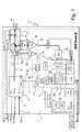
- Fig. 1shows an inventive embodiment of an optical transmitter 1 with an integrated OTDR measurement unit 2, all arranged on a common SFP board 3.
- Fig. 1shows an inventive embodiment of an optical transmitter 1 with an integrated OTDR measurement unit 2, all arranged on a common SFP board 3.
- the optical transmitter 1comprises a laser diode (LD) driver chip 4, which receives a data signal 5 at a data input 6.
- the LD driver chip 4also receives a sine wave signal 7 at a modulation input 8.
- the LD driver chip 4modulates the sine wave signal 7 on top of the data signal 5, and thus generates a modulated signal 9.
- the optical transmitter 1further comprises a laser diode 10, with a directly attached monitor diode 11.
- the monitor diode 11is typically located at a semitransparent mirror of the laser resonator of the laser diode 10.
- the laser diode 10transforms the electrical modulated signal 9 into a modulated optical output signal 12, which is fed into an optical module 13. However, part of the modulated optical output signal 12 is received and monitored by the monitor diode 11 before entering the optical module 13.
- the optical module 13guides the modulated optical output signal 12 through two beam splitters 14, 15 and into an optical fiber 16.
- the optical fiber 16transports the modulated optical output signal 12 to a distant receiver, where the information of the data signal 5 is needed.
- the OTDR measurement unit 2comprises a digital processing unit 17 (e.g. an ASIC) with a sine wave generator 18, generating a digital sine wave signal.
- the frequency of the digital sine wave signalis swept over a predefined frequency range, and a new sweep is begun every time after one sweep has been completed.
- the digital sine wave signalhas a constant amplitude in this embodiment, as determined by a gain control unit 19.
- the digital sine wave signalis converted into an analogue sine wave signal by a DAC unit 20, and the analogue sine wave signal is fed into an amplifier 21.
- the amplitude of the analogue sine wave signalis amplified according to the demands of a control circuit 22.
- the amplified analogue sine wave signalrepresents the sine wave signal 7 fed into the LD driver chip 4.
- the monitor diode 11provides a monitor signal 23 to a trans impedance amplifier (TIA) 24, and the amplified monitor signal 25 is provided to the control circuit 22.
- the modulation amplitude of the modulated optical output signal 12is determined and compared to a predefined (and here fixed) target value. If the modulation amplitude is too low, the control circuit 22 demands a higher amplification factor at amplifier 21, and if the modulation amplitude is too high, the control circuit 22 demands a lower amplification factor.
- the control circuit 22may be realized as a PID controller.
- the amplifier 21, the monitor diode 11, the TIA 24, and the control circuit 22represent an analogue control loop 30 for the amplitude of the sine wave signal 7.
- the control loop 30is permanently operating in this embodiment, actively controlling the amplitude of the sine wave signal 7 during every frequency sweep.
- the modulated optical output signal 12is partly backscattered in the optical fiber 16. This backscattered light is partially deflected by beam splitter 14 into an OTDR photo diode 26.
- the OTDR photo diode 26is separate from the monitor diode 11.
- the detection signal of the OTDR photo diode 26is amplified by TIA 27 and fed into the digital processing unit 17 via an ADC unit 28. Information about the detection signal, and thus the OTDR characteristics of the optical fiber 16, is provided by an I 2 C data interface 29 of the digital processing unit 17.
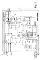
- Fig. 2shows a similar embodiment of an optical transmitter 1 with an integrated OTDR measurement unit 2, but with a digital control loop 31. Only the differences to the embodiment of Fig. 1 are described.
- the monitor diode 11provides its monitor signal 23 to TIA 24 again, and the amplified monitor signal 25a is fed via ADC unit 28a into digital processing unit 17, e.g. an ASIC.
- digital processing unit 17e.g. an ASIC.
- the modulation amplitude of the modulated optical output signal 12is determined and compared to a predefined target value corresponding to the current frequency of the sine wave generator 18.
- the set of predefined target values for every frequency within the predefined frequency rangeforms a predefined value distribution that is stored in and made available by a value distribution storage (VDS) 36 of the processing unit 17.
- VDSvalue distribution storage
- the amplitude of the digital sine wave signal generated at sine wave generator 18is increased by the gain control unit 19a. If the modulation amplitude is higher than the target value, the amplitude of the digital sine wave signal is lowered by gain control 19a.
- the digital sine wave signalis fed into DAC unit 20.
- the converted analogue sine wave signalrepresents the sine wave signal 7 fed into the LD driver chip 4.
- ADC unit 28ais also used for converting the amplified detection signal of the OTDR photo diode 26.
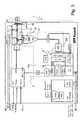
- Fig. 3shows a further embodiment of an optical transmitter 1 with an integrated OTDR measurement unit 2 similar to Fig. 2, but with a different monitoring device in a digital control loop 31b. Only the differences to Fig. 2 are described.
- the OTDR photo diode 26As a monitoring device for the modulated optical output signal 12, the OTDR photo diode 26 is used.
- a semitransparent reflector 35located before the end of the optical fiber 16, reflects a small part of the modulated optical output signal 12 leaving the optical module 13 back into the optical module 13, so that the beam splitter 14 deflects some of the modulated optical output signal 12 onto the OTDR photo diode 26.
- the detection signal of the OTDR photo diode 26, which carries information about the modulation amplitude of the modulated optical output signal 12,is amplified in TIA 27 and fed into the digital processing unit 17 via ADC unit 28a.
- the modulation amplitude of the modulated optical output signal 12is determined and used as known form the embodiment of Fig. 2.
- Fig. 4shows a further embodiment of an optical transmitter 1 with an integrated OTDR measurement unit 2 similar to Fig. 2, but with a different modulation device and a memory 34. Only the differences to Fig. 2 are described.
- the modulation of the data signal 5 and the sine wave signal 7is done by a modulation transistor 32, which adds the sine wave signal 7 to an output signal 33 of the LD driver chip 4c, thus generating the modulated signal 9.
- the LD driver chip 4cbasically forwards the data signal 5, thus generating the output signal 33.
- modulation transistor 32basically does not affect the functioning of the digital control loop 31.
- the digital processing unit 17comprises a memory 34 for storing the amplitude values used by the gain control unit 19a for the digital sine wave signal during a first frequency sweep, during which the modulated optical output signal has been monitored and the amplitude of the sine wave signal has concurrently been adjusted according to the monitoring results. For every frequency during the first frequency sweep, an amplitude value has been stored.
- the memory 34is connected to the sine wave generator 18 via the gain control unit 19a on the digital processing unit 17, and the stored amplitude values can be applied by the sine wave generator 18 during a number of frequency sweeps subsequent to the first frequency sweep.
- the monitoring of the modulated optical output signal 12 and its analysis in the digital processing unit 17is suspended, saving system resources. After a few subsequent frequency sweeps, another first frequency sweep is performed, and the stored amplitude values are updated.
Landscapes
- Physics & Mathematics (AREA)
- Electromagnetism (AREA)
- Engineering & Computer Science (AREA)
- Computer Networks & Wireless Communication (AREA)
- Signal Processing (AREA)
- Optical Communication System (AREA)
- Tests Of Electronic Circuits (AREA)
- Measurement Of Resistance Or Impedance (AREA)
- Test And Diagnosis Of Digital Computers (AREA)
Abstract
Description
- The invention relates to a method of swept sine wave OTDR (optical time domain reflectometry) measurement,
wherein a data signal, which carries payload data, is modulated by a sine wave signal on top of the payload data of the data signal, thus generating a modulated optical output signal,
wherein the sine wave signal is swept within a defined frequency range. - Such a method is known from the ITG-Konferenz "Breitbandversorgung in Deutschland - wie schaffen wir Anschluss?", presentation "Kostengünstige integrierte Glasfaserüberwachung-jederzeit und überall", J. Hehmann, H. Schmuck and T. Pfeiffer, Berlin, 12./13.10.2005.
- Optical fibers, such as glass fibers, are used to transport data. OTDR is a method of surveying the physical condition of an optical fiber, e.g. to find sharp bends or breaks limiting or preventing data traffic. Optical signals are sent down the optical fiber, and are reflected at a location of a disturbance. The run time of the backscattered optical signal can be analysed to find the distance of the disturbance from the input location of the optical signals.
- In simple OTDR implementations, a single optical signal is sent down the optical fiber, and the backscattered signal is recorded as a function of time. The delay between input of the optical signal and the arrival of a reflection from a disturbance is measured directly. However, this implementation requires an interruption in the data traffic depending on the fiber length. A 20 km long fiber link requires an interruption time of about 400 µs per measurement.
- A more advanced OTDR method, as known from the mentioned presentation at the ITG-Konferenz, modulates a sine wave signal on top of a regular data signal. The frequency of the sine wave signal is swept, typically in kHz steps up to the MHz range. The received backscattered signal undergoes a Fourier transformation, after which a time delay can be determined. The swept sine wave OTDR method requires more effort at signal processing, but can in principle be done without an interruption of the data transfer.
- In order to avoid misinterpretation of OTDR measurement results, sine wave OTDR must be performed with a constant modulation amplitude of the modulated optical output signal over the whole frequency range. Unfortunately, the electronic and optical equipment for the OTDR measurement usually shows a frequency dependent behaviour. In addition, over longer time periods, the points of operation (such as the laser bias) may change, in particular due to temperature variations of the environment and aging of the equipment.
- In the state of the art it is known to calibrate the amplitude of the sine wave signal (which is modulated onto the data signal) prior to an OTDR measurement, such that a constant modulation amplitude of the modulated optical output signal results. However, such a calibration test run of the equipment requires an interruption of the data traffic, and numerous regular calibration test runs are necessary to compensate for long term effects.
- It is also known to perform a calibration with out of band wavelengths. Then no interruption of the data traffic is necessary, but the calibration test run has a low force of expression only; in other words the calibration is rather inaccurate.
- It is the object of the invention to introduce a method of swept sine wave OTDR which allows an accurate calibration of the OTDR measurement equipment without an interruption of the data traffic.
- This object is achieved, in accordance with the invention, by a method as introduced in the beginning, characterized in that the modulation amplitude of the modulated optical output signal is monitored, and the amplitude of the sine wave signal is controlled in dependence of the modulation amplitude of the modulated optical output signal monitored during the present frequency sweep such that the monitored modulation amplitude of the modulated optical output signal matches a predefined value distribution over the whole frequency range.
- With the inventive method, the self-characteristics of the measurement equipment are compensated by a control loop. According to the invention, the amplitude of the sine wave signal is determined with the aid of a the control loop. The amplitude of the sine wave signal is altered until a desired modulation amplitude, according to the predefined value distribution, of the modulated optical output signal is registered; this is done at every frequency during a sweep. During a frequency sweep, the frequency may be changed in steps of 1 kHz, for example. As a result, an adequate amplitude of the sine wave signal is found for every frequency. The OTDR measurement then has a defined modulation amplitude of the modulated optical output signal over the whole frequency range, and no misinterpretations of the OTDR measurement results will occur. In case of a non-constant predefined value distribution, e.g. a modulation amplitude linearly increasing or decreasing with the frequency, the ODTR measurement results may easily be converted, i.e. weighted, for OTDR interpretation.
- The control loop can be operated without restriction during normal data traffic. No loss of data occurs due to the control loop.
- According to the invention, OTDR measurements are performed continuously during data transfer, so that disturbances in the optical fiber surveyed are found immediately. Typically a modulation depth of between 5% and 15%, preferably about 10% is used (modulation depth is the ratio between the amplitude of the sine wave signal and the total amplitude of the modulated signal). In case of a fiber break, i.e. when no data transfer is possible over the fiber, a modulation depth of 100% can be applied (i.e. no data signal is used) in order to reestablish the OTDR measurement the faster. Typically, the defined frequency range comprises an interval from 5 kHz up to 5 MHz. In other inventive applications, a defined frequency range of e.g. from 100 Hz up to 20 MHz may be useful. Note that a frequency sweep consists one complete tuning through the defined frequency range.
- In a preferred variant of the inventive method, the predefined value distribution is a constant modulation amplitude over the whole frequency range. In other words, the modulation amplitude of the modulated optical output signal is kept constant over the whole frequency range. This simplifies the analysis of the OTDR measurement results. In particular, no conversions are necessary.
- A particularly preferred variant of the inventive method is characterized in that the modulation amplitude of the modulated optical output signal is monitored during every frequency sweep, and that the amplitude of the sine wave signal is controlled in dependence of modulation amplitude of the modulated optical output signal monitored during the present frequency sweep. This variant represents a closed control loop. The amplitude of the sine wave signal is adapted continuously to the currently monitored modulation amplitude of the modulated optical output signal. With this variant, changes in the characteristics of the measurement equipment are immediately compensated.
- An alternative, advantageous variant of the inventive method is characterized in that the amplitude of the sine wave signal is recorded as a function of frequency during a first frequency sweep, during which the amplitude of the sine wave signal is controlled in dependence of the modulation amplitude of the modulated optical output signal monitored during the present first frequency sweep, and that during a number of frequency sweeps subsequent to the first frequency sweep, the recorded amplitude is applied as the amplitude of the sine wave signal. This variant represents an open control loop. During a first frequency sweep, the control loop analyses the current modulation amplitude of the modulated optical output signal and adapts concurrently the amplitude of the sine wave signal accordingly. The amplitude of the sine wave signal is archived, e.g. in a truth table. During subsequent frequency sweeps, the amplitude of the sine wave signal is chosen according to the values of the truth table. During the subsequent frequency sweeps, monitoring of the modulation amplitude of the modulated optical output signal is unnecessary and, consequently, typically not done. A first frequency sweep is followed by a number of subsequent sweeps, followed by another first frequency sweep, followed by a number of subsequent sweeps, and so on. The most recent set of values for the amplitude of the sine wave signal is applied. The number of subsequent frequency sweeps may be constant, such as a fixed number e.g. between 10 and 1000, or it may be chosen in dependence of the difference between values of amplitudes of consecutive first frequency sweeps, with small differences resulting in large numbers of subsequent sweeps, and large differences resulting in small numbers of subsequent sweeps (or even no subsequent sweeps at all). During subsequent sweeps, some of the measurement equipment may be conserved. This variant is particularly useful if changes due to environmental changes or aging are rather slow.
- Within the scope of the present invention is also an optical transmitter for a data signal with a sweep sine wave OTDR measurement unit, comprising
- a data input for a data signal,
- a sine wave generator for generating a sine wave signal that sweeps within a predefined frequency range,
- a modulation device for modulating the sine wave signal on top of the data signal, thus generating a modulated signal,
- and a laser diode for generating a modulated optical output signal out of the modulated signal,
- Preferably, the OTDR measurement unit is integrated into the optical transmitter. This may comprise
- use of the laser of the optical transmitter by the OTDR measurement unit,
- use of a monitoring diode of the laser for monitoring the modulation amplitude of the modulated optical output signal,
- the optical transmitter and the OTDR measurement unit are located on the same board. The modulation device may comprise, in accordance with the invention, a laser diode driver chip or a transistor connected downstream of a laser diode driver chip. Further, the sine wave generator and the gain control may be located on an ASIC (application specific integrated chip) or an FPGA (free programmable gate array) or a microprocessor.
- A preferred embodiment of the inventive optical transmitter is characterized in that the control loop is designed to monitor the modulation amplitude of the modulated optical output signal during every frequency sweep, and that the control loop is further designed to control the amplitude of the sine wave signal in dependence of modulation amplitude monitored during the present frequency sweep. This embodiment is adapted for a closed control loop operation, allowing fast reaction to changes of the measurement equipment characteristics.
- An alternative, preferred embodiment of the inventive optical transmitter provides that the control loop comprises a memory for recording the amplitude of a sine wave signal as a function of frequency during a first frequency sweep, during which the amplitude of the sine wave signal is controlled in dependence of the modulation amplitude of the modulated optical output signal monitored during the present first frequency sweep, and that the memory is connected to the sine wave generator for applying the recorded amplitude as the amplitude of the sine wave signals during a number of frequency sweeps subsequent to the first frequency sweep. This embodiment is adapted for an open loop operation, allowing to conserve equipment resources.
- In a further, advantageous embodiment, the monitoring device comprises a monitor diode directly attached to the laser diode, or an OTDR photo diode of the OTDR measurement unit. The monitor diode can be co-used for regular surveying of the laser diode, and the OTDR diode can be co-used for analysing backscattered light, so the equipment is used very efficiently. Note that when using the OTDR diode as a monitoring device, measures must be taken so that some light of the laser diode gets into the OTDR diode directly, i.e. without backscattering in the optical fiber. This can be done by altering a beam splitter belonging to the OTDR diode, for example.
- A preferred, further embodiment of the inventive optical transmitter provides that the control loop is of analogue type, that an amplifier is connected downstream to the sine wave generator, and that the amplifier is connected to a control circuit which is connected to the monitoring device. This embodiment is simple in design and allows a direct, active control.
- Alternatively, an advantageous embodiment is characterized in that the control loop is of digital type, that a gain control unit of the sine wave generator is connected to the monitoring device via an ADC (analogue to digital conversion) unit, and that a DAC (digital to analogue conversion) unit is connected downstream of the sine wave generator. This embodiment facilitates a recording of amplitude values for an open control loop operation mode.
- Further advantages can be extracted from the description and the enclosed drawing. The features mentioned above and below can be used in accordance with the invention either individually or collectively in any combination. The embodiments mentioned are not to be understood as exhaustive enumeration but rather have exemplary character for the description of the invention.
- The invention is shown in the drawing.
- Fig. 1
- shows a block diagram of an inventive embodiment of an optical transmitter with an embedded OTDR measurement unit, with an analogue control loop using a monitor diode as monitoring device;
- Fig. 2
- shows a block diagram of another inventive embodiment, with a digital control loop using a monitor diode as monitoring device;
- Fig. 3
- shown a block diagram of another inventive embodiment, with a digital control loop using an OTDR photo diode as a monitoring device;
- Fig. 4
- shows a block diagram of another inventive embodiment, with a digital control loop using a monitor diode as monitoring device, with a modulation transistor and a memory for amplitude values of the sine wave signal.
- Fig. 1 shows an inventive embodiment of an
optical transmitter 1 with an integratedOTDR measurement unit 2, all arranged on acommon SFP board 3. In the following, some functions of particular relevance for the invention are explained. An expert in the field, however, will extract many more details from the figure (and subsequent figures), which all contribute to the invention. - The
optical transmitter 1 comprises a laser diode (LD)driver chip 4, which receives adata signal 5 at a data input 6. TheLD driver chip 4 also receives a sine wave signal 7 at amodulation input 8. TheLD driver chip 4 modulates the sine wave signal 7 on top of the data signal 5, and thus generates a modulatedsignal 9. - The
optical transmitter 1 further comprises alaser diode 10, with a directly attachedmonitor diode 11. Themonitor diode 11 is typically located at a semitransparent mirror of the laser resonator of thelaser diode 10. Thelaser diode 10 transforms the electrical modulatedsignal 9 into a modulatedoptical output signal 12, which is fed into anoptical module 13. However, part of the modulatedoptical output signal 12 is received and monitored by themonitor diode 11 before entering theoptical module 13. Theoptical module 13 guides the modulatedoptical output signal 12 through twobeam splitters optical fiber 16. Theoptical fiber 16 transports the modulatedoptical output signal 12 to a distant receiver, where the information of the data signal 5 is needed. - Integrated into the
optical transmitter 1 is theOTDR measurement unit 2. TheOTDR measurement unit 2 comprises a digital processing unit 17 (e.g. an ASIC) with asine wave generator 18, generating a digital sine wave signal. The frequency of the digital sine wave signal is swept over a predefined frequency range, and a new sweep is begun every time after one sweep has been completed. The digital sine wave signal has a constant amplitude in this embodiment, as determined by again control unit 19. The digital sine wave signal is converted into an analogue sine wave signal by aDAC unit 20, and the analogue sine wave signal is fed into anamplifier 21. The amplitude of the analogue sine wave signal is amplified according to the demands of acontrol circuit 22. The amplified analogue sine wave signal represents the sine wave signal 7 fed into theLD driver chip 4. - The
monitor diode 11 provides amonitor signal 23 to a trans impedance amplifier (TIA) 24, and the amplifiedmonitor signal 25 is provided to thecontrol circuit 22. Within thecontrol circuit 22, the modulation amplitude of the modulatedoptical output signal 12 is determined and compared to a predefined (and here fixed) target value. If the modulation amplitude is too low, thecontrol circuit 22 demands a higher amplification factor atamplifier 21, and if the modulation amplitude is too high, thecontrol circuit 22 demands a lower amplification factor. Thecontrol circuit 22 may be realized as a PID controller. - The
amplifier 21, themonitor diode 11, theTIA 24, and thecontrol circuit 22 represent ananalogue control loop 30 for the amplitude of the sine wave signal 7. Thecontrol loop 30 is permanently operating in this embodiment, actively controlling the amplitude of the sine wave signal 7 during every frequency sweep. - The modulated
optical output signal 12 is partly backscattered in theoptical fiber 16. This backscattered light is partially deflected bybeam splitter 14 into anOTDR photo diode 26. TheOTDR photo diode 26 is separate from themonitor diode 11. The detection signal of theOTDR photo diode 26 is amplified byTIA 27 and fed into thedigital processing unit 17 via anADC unit 28. Information about the detection signal, and thus the OTDR characteristics of theoptical fiber 16, is provided by an I2C data interface 29 of thedigital processing unit 17. - Fig. 2 shows a similar embodiment of an
optical transmitter 1 with an integratedOTDR measurement unit 2, but with adigital control loop 31. Only the differences to the embodiment of Fig. 1 are described. - The
monitor diode 11 provides itsmonitor signal 23 toTIA 24 again, and the amplifiedmonitor signal 25a is fed viaADC unit 28a intodigital processing unit 17, e.g. an ASIC. Within thedigital processing unit 17, the modulation amplitude of the modulatedoptical output signal 12 is determined and compared to a predefined target value corresponding to the current frequency of thesine wave generator 18. The set of predefined target values for every frequency within the predefined frequency range forms a predefined value distribution that is stored in and made available by a value distribution storage (VDS) 36 of theprocessing unit 17. Note that the valuedistribution storage VDS 36 only stores one value - and therefore may be obsolete - when the predefined value distribution is a constant modulation amplitude over the whole frequency range. If the modulation amplitude is lower than the target value, then the amplitude of the digital sine wave signal generated atsine wave generator 18 is increased by thegain control unit 19a. If the modulation amplitude is higher than the target value, the amplitude of the digital sine wave signal is lowered bygain control 19a. The digital sine wave signal is fed intoDAC unit 20. The converted analogue sine wave signal represents the sine wave signal 7 fed into theLD driver chip 4. - Note that
ADC unit 28a is also used for converting the amplified detection signal of theOTDR photo diode 26. - Fig. 3 shows a further embodiment of an
optical transmitter 1 with an integratedOTDR measurement unit 2 similar to Fig. 2, but with a different monitoring device in adigital control loop 31b. Only the differences to Fig. 2 are described. - As a monitoring device for the modulated
optical output signal 12, theOTDR photo diode 26 is used. Asemitransparent reflector 35, located before the end of theoptical fiber 16, reflects a small part of the modulatedoptical output signal 12 leaving theoptical module 13 back into theoptical module 13, so that thebeam splitter 14 deflects some of the modulatedoptical output signal 12 onto theOTDR photo diode 26. The detection signal of theOTDR photo diode 26, which carries information about the modulation amplitude of the modulatedoptical output signal 12, is amplified inTIA 27 and fed into thedigital processing unit 17 viaADC unit 28a. - Within the
digital processing unit 17, the modulation amplitude of the modulatedoptical output signal 12 is determined and used as known form the embodiment of Fig. 2. - Fig. 4 shows a further embodiment of an
optical transmitter 1 with an integratedOTDR measurement unit 2 similar to Fig. 2, but with a different modulation device and amemory 34. Only the differences to Fig. 2 are described. - The modulation of the data signal 5 and the sine wave signal 7 is done by a
modulation transistor 32, which adds the sine wave signal 7 to anoutput signal 33 of theLD driver chip 4c, thus generating the modulatedsignal 9. TheLD driver chip 4c basically forwards the data signal 5, thus generating theoutput signal 33. - Note that the
modulation transistor 32 basically does not affect the functioning of thedigital control loop 31. - In the embodiment of Fig. 4, the
digital processing unit 17 comprises amemory 34 for storing the amplitude values used by thegain control unit 19a for the digital sine wave signal during a first frequency sweep, during which the modulated optical output signal has been monitored and the amplitude of the sine wave signal has concurrently been adjusted according to the monitoring results. For every frequency during the first frequency sweep, an amplitude value has been stored. Thememory 34 is connected to thesine wave generator 18 via thegain control unit 19a on thedigital processing unit 17, and the stored amplitude values can be applied by thesine wave generator 18 during a number of frequency sweeps subsequent to the first frequency sweep. During the subsequent frequency sweeps, the monitoring of the modulatedoptical output signal 12 and its analysis in thedigital processing unit 17 is suspended, saving system resources. After a few subsequent frequency sweeps, another first frequency sweep is performed, and the stored amplitude values are updated.
Claims (10)
- Method of swept sine wave OTDR (optical time domain reflectometry) measurement,
wherein a data signal (5), which carries payload data, is modulated by a sine wave signal (7) on top of the payload data of the data signal (5), thus generating a modulated optical output signal (12),
wherein the sine wave signal (7) is swept within a defined frequency range,
characterized in that
the modulation amplitude of the modulated optical output signal (12) is monitored,
and the amplitude of the sine wave signal (7) is controlled in dependence of the modulation amplitude of the modulated optical output signal (12) monitored during the present frequency sweep such that the monitored modulation amplitude of the modulated optical output signal (12) matches a predefined value distribution over the whole frequency range. - Method according to claim 1,characterized in that the predefined value distribution is a constant modulation amplitude over the whole frequency range.
- Method according to claim 1,characterized in
that the modulation amplitude of the modulated optical output signal (12) is monitored during every frequency sweep,
andthat the amplitude of the sine wave signal (7) is controlled in dependence of modulation amplitude of the modulated optical output signal (12) monitored during the present frequency sweep. - Method according to claim 1,characterized in
that the amplitude of the sine wave signal (7) is recorded as a function of frequency during a first frequency sweep, during which the amplitude of the sine wave signal (7) is controlled in dependence of the modulation amplitude of the modulated optical output signal (12) monitored during the present first frequency sweep,
andthat during a number of frequency sweeps subsequent to the first frequency sweep, the recorded amplitude is applied as the amplitude of the sine wave signal (7). - Optical transmitter (1) for a data signal (5) with a sweep sine wave OTDR measurement unit (2), comprising- a data input (6) for a data signal (5),- a sine wave generator (18) for generating a sine wave signal (7) that sweeps within a predefined frequency range,- a modulation device for modulating the sine wave signal (7) on top of the data signal (5), thus generating a modulated signal (9),- and a laser diode (10) for generating a modulated optical output signal (12) out of the modulated signal (9),characterized in that
the optical transmitter (1) comprises a control loop (30; 31; 31b) with a monitoring device for monitoring the modulation amplitude of the modulated optical output signal (12),
wherein the control loop (30; 31; 31b) is designed for controlling the amplitude of the sine wave signal (7) in dependence of the modulation amplitude of the modulated optical output signal (12) monitored during the present frequency sweep such that the monitored modulation amplitude of the modulated optical output signal (12) matches a predefined value distribution over the whole frequency range, in particular wherein the predefined value distribution is a constant modulation amplitude over the whole frequency range. - Optical transmitter (1) according to claim 5,characterized in
that the control loop (30; 31; 31b) is designed to monitor the modulation amplitude of the modulated optical output signal (12) during every frequency sweep,
andthat the control loop (30; 31; 31b) is further designed to control the amplitude of the sine wave signal (7) in dependence of modulation amplitude monitored during the present frequency sweep. - Optical transmitter (1) according to claim 5,characterized in that
the control loop (30; 31; 31b) comprises a memory (34) for recording the amplitude of a sine wave signal (7) as a function of frequency during a first frequency sweep, during which the amplitude of the sine wave signal (7) is controlled in dependence of the modulation amplitude of the modulated optical output signal (12) monitored during the present first frequency sweep,
and that the memory (5) is connected to the sine wave generator (18) for applying the recorded amplitude as the amplitude of the sine wave signals (7) during a number of frequency sweeps subsequent to the first frequency sweep. - Optical transmitter (1) according to claim 5,characterized in that the monitoring device comprises a monitor diode (11) directly attached to the laser diode (10), or an OTDR photo diode (26) of the OTDR measurement unit (2).
- Optical transmitter (1) according to claim 5,characterized in
that the control loop (30) is of analogue type,
that an amplifier (21) is connected downstream to the sine wave generator (18), and that the amplifier (21) is connected to a control circuit (22) which is connected to the monitoring device. - Optical transmitter (1) according to claim 5,characterized in
that the control loop (31; 31b) is of digital type,
that a gain control unit (19a) of the sine wave generator (18) is connected to the monitoring device via an ADC (analogue to digital conversion) unit (28a; 28b),
andthat a DAC (digital to analogue conversion) unit (20) is connected downstream of the sine wave generator (18).
Priority Applications (3)
| Application Number | Priority Date | Filing Date | Title |
|---|---|---|---|
| EP06291267AEP1884758B1 (en) | 2006-08-03 | 2006-08-03 | Control loop for the integrated sine wave OTDR measurement online |
| DE602006010058TDE602006010058D1 (en) | 2006-08-03 | 2006-08-03 | Control circuit for online OTDR measurement with integrated sine wave |
| AT06291267TATE447167T1 (en) | 2006-08-03 | 2006-08-03 | CONTROL CIRCUIT FOR ONLINE OTDR MEASUREMENT WITH INTEGRATED SINE WAVE |
Applications Claiming Priority (1)
| Application Number | Priority Date | Filing Date | Title |
|---|---|---|---|
| EP06291267AEP1884758B1 (en) | 2006-08-03 | 2006-08-03 | Control loop for the integrated sine wave OTDR measurement online |
Publications (2)
| Publication Number | Publication Date |
|---|---|
| EP1884758A1true EP1884758A1 (en) | 2008-02-06 |
| EP1884758B1 EP1884758B1 (en) | 2009-10-28 |
Family
ID=37594130
Family Applications (1)
| Application Number | Title | Priority Date | Filing Date |
|---|---|---|---|
| EP06291267ANot-in-forceEP1884758B1 (en) | 2006-08-03 | 2006-08-03 | Control loop for the integrated sine wave OTDR measurement online |
Country Status (3)
| Country | Link |
|---|---|
| EP (1) | EP1884758B1 (en) |
| AT (1) | ATE447167T1 (en) |
| DE (1) | DE602006010058D1 (en) |
Cited By (15)
| Publication number | Priority date | Publication date | Assignee | Title |
|---|---|---|---|---|
| CN102281104A (en)* | 2011-08-22 | 2011-12-14 | 中兴通讯股份有限公司 | On-line testing device and method for fiber |
| US8526824B1 (en) | 2011-03-21 | 2013-09-03 | Adtran, Inc. | Correlation systems and methods with error compensation |
| WO2013134404A1 (en)* | 2012-03-06 | 2013-09-12 | Adtran, Inc. | Optical communication devices having optical time domain reflectometers |
| US8594496B2 (en) | 2009-11-13 | 2013-11-26 | Futurewei Technologies, Inc. | Tunable coherent optical time division reflectometry |
| US8606117B1 (en) | 2010-05-20 | 2013-12-10 | Adtran, Inc. | Systems and methods for unobtrusively testing optical fibers |
| US8701161B1 (en) | 2012-06-29 | 2014-04-15 | Adtran, Inc. | Systems and methods for detecting network intrusion devices |
| US8818199B2 (en) | 2012-02-06 | 2014-08-26 | Adtran, Inc. | Correlation systems and methods with error compensation |
| US8971717B1 (en) | 2012-02-06 | 2015-03-03 | Adtran, Inc. | Optical communication systems and methods with crosstalk cancellation |
| EP2983310A1 (en)* | 2014-08-05 | 2016-02-10 | Alcatel Lucent | Device and method for use in optical time domain reflectometry measurements |
| US9350447B1 (en) | 2012-06-22 | 2016-05-24 | Adtran, Inc. | Systems and methods for protecting optical networks from rogue optical network terminals |
| WO2016118053A1 (en)* | 2015-01-21 | 2016-07-28 | Telefonaktiebolaget Lm Ericsson (Publ) | Monitoring optical fibre link |
| CN105991184A (en)* | 2015-02-05 | 2016-10-05 | 四川泰瑞创通讯技术股份有限公司 | Self-recovery method of disabled transmitting terminal of optical module during OTDR test |
| WO2016190792A1 (en)* | 2015-05-28 | 2016-12-01 | Telefonaktiebolaget Lm Ericsson (Publ) | Device and method for monitoring optical fibre link |
| US20170269138A1 (en)* | 2012-05-21 | 2017-09-21 | Amplifier Research Corporation | Field analyzer |
| WO2022083254A1 (en)* | 2020-10-23 | 2022-04-28 | 华为技术有限公司 | Frequency response estimation method and apparatus |
Citations (7)
| Publication number | Priority date | Publication date | Assignee | Title |
|---|---|---|---|---|
| EP0313020A2 (en)* | 1987-10-19 | 1989-04-26 | Anritsu Corporation | Optical time domain reflectometer with level adjusting function |
| EP0453816A2 (en)* | 1990-04-25 | 1991-10-30 | Tektronix Inc. | An improved optical time domain reflectometer having pre and post front panel connector testing capabilities |
| GB2268851A (en)* | 1992-07-17 | 1994-01-19 | Northern Telecom Ltd | Modulation depth control for FSK/IM optical transmitter |
| US6323978B1 (en)* | 1998-04-06 | 2001-11-27 | Nortel Networks Limited | Robust variable-bit-rate optical channel overhead |
| US20040070750A1 (en)* | 2002-10-09 | 2004-04-15 | Iannelli John M. | Optical time domain reflectometry system and method |
| US20040247316A1 (en)* | 2003-03-03 | 2004-12-09 | Ubi Systems, Inc. | System and method for performing in-service fiber optic network certification |
| US20050196175A1 (en)* | 2004-03-05 | 2005-09-08 | Evangelides Stephen G.Jr. | Method and apparatus for obtaining status information concerning an in-service optical transmission line |
Family Cites Families (2)
| Publication number | Priority date | Publication date | Assignee | Title |
|---|---|---|---|---|
| GB2294373B (en)* | 1992-06-10 | 1996-08-28 | Kokusai Denshin Denwa Co Ltd | Supervisory method,loopback circuit,and transmitting and receiving circuit for an optical repeater system |
| US6665500B2 (en)* | 2001-01-29 | 2003-12-16 | Oyster Optics, Inc. | Dual-mode fiber optic telecommunications system and method |
- 2006
- 2006-08-03DEDE602006010058Tpatent/DE602006010058D1/enactiveActive
- 2006-08-03EPEP06291267Apatent/EP1884758B1/ennot_activeNot-in-force
- 2006-08-03ATAT06291267Tpatent/ATE447167T1/ennot_activeIP Right Cessation
Patent Citations (7)
| Publication number | Priority date | Publication date | Assignee | Title |
|---|---|---|---|---|
| EP0313020A2 (en)* | 1987-10-19 | 1989-04-26 | Anritsu Corporation | Optical time domain reflectometer with level adjusting function |
| EP0453816A2 (en)* | 1990-04-25 | 1991-10-30 | Tektronix Inc. | An improved optical time domain reflectometer having pre and post front panel connector testing capabilities |
| GB2268851A (en)* | 1992-07-17 | 1994-01-19 | Northern Telecom Ltd | Modulation depth control for FSK/IM optical transmitter |
| US6323978B1 (en)* | 1998-04-06 | 2001-11-27 | Nortel Networks Limited | Robust variable-bit-rate optical channel overhead |
| US20040070750A1 (en)* | 2002-10-09 | 2004-04-15 | Iannelli John M. | Optical time domain reflectometry system and method |
| US20040247316A1 (en)* | 2003-03-03 | 2004-12-09 | Ubi Systems, Inc. | System and method for performing in-service fiber optic network certification |
| US20050196175A1 (en)* | 2004-03-05 | 2005-09-08 | Evangelides Stephen G.Jr. | Method and apparatus for obtaining status information concerning an in-service optical transmission line |
Cited By (23)
| Publication number | Priority date | Publication date | Assignee | Title |
|---|---|---|---|---|
| US8750703B2 (en) | 2009-11-13 | 2014-06-10 | Futurewei Technologies, Inc. | Tunable coherent optical time division reflectometry |
| US8594496B2 (en) | 2009-11-13 | 2013-11-26 | Futurewei Technologies, Inc. | Tunable coherent optical time division reflectometry |
| US8606117B1 (en) | 2010-05-20 | 2013-12-10 | Adtran, Inc. | Systems and methods for unobtrusively testing optical fibers |
| US8526824B1 (en) | 2011-03-21 | 2013-09-03 | Adtran, Inc. | Correlation systems and methods with error compensation |
| CN102281104A (en)* | 2011-08-22 | 2011-12-14 | 中兴通讯股份有限公司 | On-line testing device and method for fiber |
| CN102281104B (en)* | 2011-08-22 | 2016-07-06 | 中兴通讯股份有限公司 | A kind of optical fiber online testing device and method |
| US8818199B2 (en) | 2012-02-06 | 2014-08-26 | Adtran, Inc. | Correlation systems and methods with error compensation |
| US8971717B1 (en) | 2012-02-06 | 2015-03-03 | Adtran, Inc. | Optical communication systems and methods with crosstalk cancellation |
| WO2013134404A1 (en)* | 2012-03-06 | 2013-09-12 | Adtran, Inc. | Optical communication devices having optical time domain reflectometers |
| US9143228B2 (en) | 2012-03-06 | 2015-09-22 | Adtran, Inc. | Optical communication devices having optical time domain reflectometers |
| US20170269138A1 (en)* | 2012-05-21 | 2017-09-21 | Amplifier Research Corporation | Field analyzer |
| US9350447B1 (en) | 2012-06-22 | 2016-05-24 | Adtran, Inc. | Systems and methods for protecting optical networks from rogue optical network terminals |
| US8701161B1 (en) | 2012-06-29 | 2014-04-15 | Adtran, Inc. | Systems and methods for detecting network intrusion devices |
| EP2983310A1 (en)* | 2014-08-05 | 2016-02-10 | Alcatel Lucent | Device and method for use in optical time domain reflectometry measurements |
| WO2016118053A1 (en)* | 2015-01-21 | 2016-07-28 | Telefonaktiebolaget Lm Ericsson (Publ) | Monitoring optical fibre link |
| US10218434B2 (en) | 2015-01-21 | 2019-02-26 | Telefonaktiebolaget Lm Ericsson (Publ) | Monitoring optical fibre link |
| CN105991184A (en)* | 2015-02-05 | 2016-10-05 | 四川泰瑞创通讯技术股份有限公司 | Self-recovery method of disabled transmitting terminal of optical module during OTDR test |
| CN105991184B (en)* | 2015-02-05 | 2018-05-25 | 四川泰瑞创通讯技术股份有限公司 | The self-recovery method of OTDR transmitting terminal optical module test failures |
| WO2016190792A1 (en)* | 2015-05-28 | 2016-12-01 | Telefonaktiebolaget Lm Ericsson (Publ) | Device and method for monitoring optical fibre link |
| CN107667489A (en)* | 2015-05-28 | 2018-02-06 | 瑞典爱立信有限公司 | Apparatus and method for monitoring fiber link |
| US20180152239A1 (en)* | 2015-05-28 | 2018-05-31 | Telefonaktiebolaget Lm Ericsson (Publ) | Device and method for monitoring optical fibre link |
| US10250323B2 (en)* | 2015-05-28 | 2019-04-02 | Telefonaktiebolaget L M Ericsson (Publ) | Device and method for monitoring optical fibre link |
| WO2022083254A1 (en)* | 2020-10-23 | 2022-04-28 | 华为技术有限公司 | Frequency response estimation method and apparatus |
Also Published As
| Publication number | Publication date |
|---|---|
| ATE447167T1 (en) | 2009-11-15 |
| EP1884758B1 (en) | 2009-10-28 |
| DE602006010058D1 (en) | 2009-12-10 |
Similar Documents
| Publication | Publication Date | Title |
|---|---|---|
| EP1884758B1 (en) | Control loop for the integrated sine wave OTDR measurement online | |
| US20130208264A1 (en) | Integrated optical time domain reflectometer | |
| US4425503A (en) | Method for detecting the presence of a gas in an atmosphere | |
| US20210010836A1 (en) | Optical fiber sensor and analysis method | |
| GB2401738A (en) | Optical fibre sensor | |
| US5963313A (en) | Optical time domain reflectometer with bandwidth correction | |
| CN111198289A (en) | A kind of control method of fiber optic current measuring device | |
| CN113203886A (en) | Method for controlling gain and sensitivity of electro-optical probe | |
| KR20160096470A (en) | Optical line monitoring system with trace-baced auto gain control and method thereof | |
| EP4489329A1 (en) | Apparatus and method for measuring chirp in fiber optical transmitters | |
| US5619321A (en) | Method of and device for measuring the Kerr non-linearity coefficient in a single mode optical fiber | |
| CN102104229A (en) | Wavelength control device and method of single frequency laser | |
| CN111198299A (en) | On-site collection type optical fiber type current measuring device | |
| US11029232B2 (en) | Optical time domain reflectometer and testing method of optical time domain reflectometer | |
| Pastor-Graells et al. | Impact of the laser phase noise on chirped-pulse phase-sensitive OTDR | |
| US7016023B2 (en) | Chromatic dispersion measurement | |
| JP5061981B2 (en) | Optical pulse tester and optical power stabilization method for optical pulse tester | |
| CN109900383B (en) | Optical fiber temperature signal automatic gain device and optical fiber temperature demodulator | |
| JP5325848B2 (en) | Optical pulse test apparatus and optical transmission line test method | |
| JP5715181B2 (en) | Optical pulse test equipment | |
| US7953320B2 (en) | Systems and methods for determining an AC/DC cross-calibration coefficient | |
| JPH07174666A (en) | Otdr for automatic setting of pulse width and gain | |
| JPH1151808A (en) | Measuring apparatus | |
| WO2022162718A1 (en) | Brillouin gain spectrum distribution measurement method and device | |
| JP3599693B2 (en) | Optical pulse test equipment |
Legal Events
| Date | Code | Title | Description |
|---|---|---|---|
| PUAI | Public reference made under article 153(3) epc to a published international application that has entered the european phase | Free format text:ORIGINAL CODE: 0009012 | |
| 17P | Request for examination filed | Effective date:20070525 | |
| AK | Designated contracting states | Kind code of ref document:A1 Designated state(s):AT BE BG CH CY CZ DE DK EE ES FI FR GB GR HU IE IS IT LI LT LU LV MC NL PL PT RO SE SI SK TR | |
| AX | Request for extension of the european patent | Extension state:AL BA HR MK YU | |
| AKX | Designation fees paid | Designated state(s):AT BE BG CH CY CZ DE DK EE ES FI FR GB GR HU IE IS IT LI LT LU LV MC NL PL PT RO SE SI SK TR | |
| GRAP | Despatch of communication of intention to grant a patent | Free format text:ORIGINAL CODE: EPIDOSNIGR1 | |
| GRAS | Grant fee paid | Free format text:ORIGINAL CODE: EPIDOSNIGR3 | |
| GRAA | (expected) grant | Free format text:ORIGINAL CODE: 0009210 | |
| AK | Designated contracting states | Kind code of ref document:B1 Designated state(s):AT BE BG CH CY CZ DE DK EE ES FI FR GB GR HU IE IS IT LI LT LU LV MC NL PL PT RO SE SI SK TR | |
| REG | Reference to a national code | Ref country code:GB Ref legal event code:FG4D | |
| REG | Reference to a national code | Ref country code:CH Ref legal event code:EP | |
| REG | Reference to a national code | Ref country code:IE Ref legal event code:FG4D | |
| REF | Corresponds to: | Ref document number:602006010058 Country of ref document:DE Date of ref document:20091210 Kind code of ref document:P | |
| LTIE | Lt: invalidation of european patent or patent extension | Effective date:20091028 | |
| NLV1 | Nl: lapsed or annulled due to failure to fulfill the requirements of art. 29p and 29m of the patents act | ||
| PG25 | Lapsed in a contracting state [announced via postgrant information from national office to epo] | Ref country code:SE Free format text:LAPSE BECAUSE OF FAILURE TO SUBMIT A TRANSLATION OF THE DESCRIPTION OR TO PAY THE FEE WITHIN THE PRESCRIBED TIME-LIMIT Effective date:20091028 Ref country code:FI Free format text:LAPSE BECAUSE OF FAILURE TO SUBMIT A TRANSLATION OF THE DESCRIPTION OR TO PAY THE FEE WITHIN THE PRESCRIBED TIME-LIMIT Effective date:20091028 Ref country code:IS Free format text:LAPSE BECAUSE OF FAILURE TO SUBMIT A TRANSLATION OF THE DESCRIPTION OR TO PAY THE FEE WITHIN THE PRESCRIBED TIME-LIMIT Effective date:20100228 Ref country code:PT Free format text:LAPSE BECAUSE OF FAILURE TO SUBMIT A TRANSLATION OF THE DESCRIPTION OR TO PAY THE FEE WITHIN THE PRESCRIBED TIME-LIMIT Effective date:20100301 Ref country code:ES Free format text:LAPSE BECAUSE OF FAILURE TO SUBMIT A TRANSLATION OF THE DESCRIPTION OR TO PAY THE FEE WITHIN THE PRESCRIBED TIME-LIMIT Effective date:20100208 Ref country code:LT Free format text:LAPSE BECAUSE OF FAILURE TO SUBMIT A TRANSLATION OF THE DESCRIPTION OR TO PAY THE FEE WITHIN THE PRESCRIBED TIME-LIMIT Effective date:20091028 | |
| PG25 | Lapsed in a contracting state [announced via postgrant information from national office to epo] | Ref country code:CY Free format text:LAPSE BECAUSE OF FAILURE TO SUBMIT A TRANSLATION OF THE DESCRIPTION OR TO PAY THE FEE WITHIN THE PRESCRIBED TIME-LIMIT Effective date:20091028 Ref country code:PL Free format text:LAPSE BECAUSE OF FAILURE TO SUBMIT A TRANSLATION OF THE DESCRIPTION OR TO PAY THE FEE WITHIN THE PRESCRIBED TIME-LIMIT Effective date:20091028 Ref country code:SI Free format text:LAPSE BECAUSE OF FAILURE TO SUBMIT A TRANSLATION OF THE DESCRIPTION OR TO PAY THE FEE WITHIN THE PRESCRIBED TIME-LIMIT Effective date:20091028 Ref country code:LV Free format text:LAPSE BECAUSE OF FAILURE TO SUBMIT A TRANSLATION OF THE DESCRIPTION OR TO PAY THE FEE WITHIN THE PRESCRIBED TIME-LIMIT Effective date:20091028 | |
| PG25 | Lapsed in a contracting state [announced via postgrant information from national office to epo] | Ref country code:BE Free format text:LAPSE BECAUSE OF FAILURE TO SUBMIT A TRANSLATION OF THE DESCRIPTION OR TO PAY THE FEE WITHIN THE PRESCRIBED TIME-LIMIT Effective date:20091028 Ref country code:AT Free format text:LAPSE BECAUSE OF FAILURE TO SUBMIT A TRANSLATION OF THE DESCRIPTION OR TO PAY THE FEE WITHIN THE PRESCRIBED TIME-LIMIT Effective date:20091028 | |
| PG25 | Lapsed in a contracting state [announced via postgrant information from national office to epo] | Ref country code:BG Free format text:LAPSE BECAUSE OF FAILURE TO SUBMIT A TRANSLATION OF THE DESCRIPTION OR TO PAY THE FEE WITHIN THE PRESCRIBED TIME-LIMIT Effective date:20100128 Ref country code:EE Free format text:LAPSE BECAUSE OF FAILURE TO SUBMIT A TRANSLATION OF THE DESCRIPTION OR TO PAY THE FEE WITHIN THE PRESCRIBED TIME-LIMIT Effective date:20091028 Ref country code:RO Free format text:LAPSE BECAUSE OF FAILURE TO SUBMIT A TRANSLATION OF THE DESCRIPTION OR TO PAY THE FEE WITHIN THE PRESCRIBED TIME-LIMIT Effective date:20091028 Ref country code:DK Free format text:LAPSE BECAUSE OF FAILURE TO SUBMIT A TRANSLATION OF THE DESCRIPTION OR TO PAY THE FEE WITHIN THE PRESCRIBED TIME-LIMIT Effective date:20091028 | |
| PG25 | Lapsed in a contracting state [announced via postgrant information from national office to epo] | Ref country code:SK Free format text:LAPSE BECAUSE OF FAILURE TO SUBMIT A TRANSLATION OF THE DESCRIPTION OR TO PAY THE FEE WITHIN THE PRESCRIBED TIME-LIMIT Effective date:20091028 Ref country code:CZ Free format text:LAPSE BECAUSE OF FAILURE TO SUBMIT A TRANSLATION OF THE DESCRIPTION OR TO PAY THE FEE WITHIN THE PRESCRIBED TIME-LIMIT Effective date:20091028 | |
| PLBE | No opposition filed within time limit | Free format text:ORIGINAL CODE: 0009261 | |
| STAA | Information on the status of an ep patent application or granted ep patent | Free format text:STATUS: NO OPPOSITION FILED WITHIN TIME LIMIT | |
| 26N | No opposition filed | Effective date:20100729 | |
| PG25 | Lapsed in a contracting state [announced via postgrant information from national office to epo] | Ref country code:GR Free format text:LAPSE BECAUSE OF FAILURE TO SUBMIT A TRANSLATION OF THE DESCRIPTION OR TO PAY THE FEE WITHIN THE PRESCRIBED TIME-LIMIT Effective date:20100129 | |
| PG25 | Lapsed in a contracting state [announced via postgrant information from national office to epo] | Ref country code:MC Free format text:LAPSE BECAUSE OF NON-PAYMENT OF DUE FEES Effective date:20100831 Ref country code:IT Free format text:LAPSE BECAUSE OF FAILURE TO SUBMIT A TRANSLATION OF THE DESCRIPTION OR TO PAY THE FEE WITHIN THE PRESCRIBED TIME-LIMIT Effective date:20091028 | |
| REG | Reference to a national code | Ref country code:CH Ref legal event code:PL | |
| PG25 | Lapsed in a contracting state [announced via postgrant information from national office to epo] | Ref country code:LI Free format text:LAPSE BECAUSE OF NON-PAYMENT OF DUE FEES Effective date:20100831 Ref country code:CH Free format text:LAPSE BECAUSE OF NON-PAYMENT OF DUE FEES Effective date:20100831 | |
| PG25 | Lapsed in a contracting state [announced via postgrant information from national office to epo] | Ref country code:IE Free format text:LAPSE BECAUSE OF NON-PAYMENT OF DUE FEES Effective date:20100803 | |
| PG25 | Lapsed in a contracting state [announced via postgrant information from national office to epo] | Ref country code:NL Free format text:LAPSE BECAUSE OF FAILURE TO SUBMIT A TRANSLATION OF THE DESCRIPTION OR TO PAY THE FEE WITHIN THE PRESCRIBED TIME-LIMIT Effective date:20091028 Ref country code:HU Free format text:LAPSE BECAUSE OF FAILURE TO SUBMIT A TRANSLATION OF THE DESCRIPTION OR TO PAY THE FEE WITHIN THE PRESCRIBED TIME-LIMIT Effective date:20100429 Ref country code:LU Free format text:LAPSE BECAUSE OF NON-PAYMENT OF DUE FEES Effective date:20100803 | |
| PG25 | Lapsed in a contracting state [announced via postgrant information from national office to epo] | Ref country code:TR Free format text:LAPSE BECAUSE OF FAILURE TO SUBMIT A TRANSLATION OF THE DESCRIPTION OR TO PAY THE FEE WITHIN THE PRESCRIBED TIME-LIMIT Effective date:20091028 | |
| REG | Reference to a national code | Ref country code:FR Ref legal event code:GC Effective date:20131018 | |
| REG | Reference to a national code | Ref country code:FR Ref legal event code:RG Effective date:20141016 | |
| REG | Reference to a national code | Ref country code:FR Ref legal event code:CA Effective date:20150521 | |
| REG | Reference to a national code | Ref country code:FR Ref legal event code:CA Effective date:20150521 | |
| REG | Reference to a national code | Ref country code:FR Ref legal event code:PLFP Year of fee payment:10 | |
| REG | Reference to a national code | Ref country code:FR Ref legal event code:PLFP Year of fee payment:11 | |
| REG | Reference to a national code | Ref country code:FR Ref legal event code:PLFP Year of fee payment:12 | |
| PGFP | Annual fee paid to national office [announced via postgrant information from national office to epo] | Ref country code:FR Payment date:20170511 Year of fee payment:9 | |
| REG | Reference to a national code | Ref country code:GB Ref legal event code:732E Free format text:REGISTERED BETWEEN 20190429 AND 20190502 | |
| REG | Reference to a national code | Ref country code:DE Ref legal event code:R082 Ref document number:602006010058 Country of ref document:DE Representative=s name:MENZIETTI WETZEL, DE Ref country code:DE Ref legal event code:R081 Ref document number:602006010058 Country of ref document:DE Owner name:PROVENANCE ASSET GROUP LLC, PITTSFORD, US Free format text:FORMER OWNER: ALCATEL LUCENT, PARIS, FR | |
| PG25 | Lapsed in a contracting state [announced via postgrant information from national office to epo] | Ref country code:FR Free format text:LAPSE BECAUSE OF NON-PAYMENT OF DUE FEES Effective date:20180831 | |
| PGFP | Annual fee paid to national office [announced via postgrant information from national office to epo] | Ref country code:DE Payment date:20200901 Year of fee payment:15 | |
| PGFP | Annual fee paid to national office [announced via postgrant information from national office to epo] | Ref country code:GB Payment date:20201029 Year of fee payment:15 | |
| REG | Reference to a national code | Ref country code:DE Ref legal event code:R119 Ref document number:602006010058 Country of ref document:DE | |
| GBPC | Gb: european patent ceased through non-payment of renewal fee | Effective date:20210803 | |
| PG25 | Lapsed in a contracting state [announced via postgrant information from national office to epo] | Ref country code:GB Free format text:LAPSE BECAUSE OF NON-PAYMENT OF DUE FEES Effective date:20210803 Ref country code:DE Free format text:LAPSE BECAUSE OF NON-PAYMENT OF DUE FEES Effective date:20220301 |