EP1870767B1 - Verically-aligned (VA) liquid crystal display device - Google Patents
Verically-aligned (VA) liquid crystal display deviceDownload PDFInfo
- Publication number
- EP1870767B1 EP1870767B1EP07113497AEP07113497AEP1870767B1EP 1870767 B1EP1870767 B1EP 1870767B1EP 07113497 AEP07113497 AEP 07113497AEP 07113497 AEP07113497 AEP 07113497AEP 1870767 B1EP1870767 B1EP 1870767B1
- Authority
- EP
- European Patent Office
- Prior art keywords
- liquid crystal
- pixel
- protrusions
- crystal display
- display device
- Prior art date
- Legal status (The legal status is an assumption and is not a legal conclusion. Google has not performed a legal analysis and makes no representation as to the accuracy of the status listed.)
- Expired - Lifetime
Links
Images


Classifications
- G—PHYSICS
- G02—OPTICS
- G02F—OPTICAL DEVICES OR ARRANGEMENTS FOR THE CONTROL OF LIGHT BY MODIFICATION OF THE OPTICAL PROPERTIES OF THE MEDIA OF THE ELEMENTS INVOLVED THEREIN; NON-LINEAR OPTICS; FREQUENCY-CHANGING OF LIGHT; OPTICAL LOGIC ELEMENTS; OPTICAL ANALOGUE/DIGITAL CONVERTERS
- G02F1/00—Devices or arrangements for the control of the intensity, colour, phase, polarisation or direction of light arriving from an independent light source, e.g. switching, gating or modulating; Non-linear optics
- G02F1/01—Devices or arrangements for the control of the intensity, colour, phase, polarisation or direction of light arriving from an independent light source, e.g. switching, gating or modulating; Non-linear optics for the control of the intensity, phase, polarisation or colour
- G02F1/13—Devices or arrangements for the control of the intensity, colour, phase, polarisation or direction of light arriving from an independent light source, e.g. switching, gating or modulating; Non-linear optics for the control of the intensity, phase, polarisation or colour based on liquid crystals, e.g. single liquid crystal display cells
- G02F1/133—Constructional arrangements; Operation of liquid crystal cells; Circuit arrangements
- G02F1/1333—Constructional arrangements; Manufacturing methods
- G02F1/1337—Surface-induced orientation of the liquid crystal molecules, e.g. by alignment layers
- G02F1/133753—Surface-induced orientation of the liquid crystal molecules, e.g. by alignment layers with different alignment orientations or pretilt angles on a same surface, e.g. for grey scale or improved viewing angle
- G—PHYSICS
- G02—OPTICS
- G02F—OPTICAL DEVICES OR ARRANGEMENTS FOR THE CONTROL OF LIGHT BY MODIFICATION OF THE OPTICAL PROPERTIES OF THE MEDIA OF THE ELEMENTS INVOLVED THEREIN; NON-LINEAR OPTICS; FREQUENCY-CHANGING OF LIGHT; OPTICAL LOGIC ELEMENTS; OPTICAL ANALOGUE/DIGITAL CONVERTERS
- G02F1/00—Devices or arrangements for the control of the intensity, colour, phase, polarisation or direction of light arriving from an independent light source, e.g. switching, gating or modulating; Non-linear optics
- G02F1/01—Devices or arrangements for the control of the intensity, colour, phase, polarisation or direction of light arriving from an independent light source, e.g. switching, gating or modulating; Non-linear optics for the control of the intensity, phase, polarisation or colour
- G02F1/13—Devices or arrangements for the control of the intensity, colour, phase, polarisation or direction of light arriving from an independent light source, e.g. switching, gating or modulating; Non-linear optics for the control of the intensity, phase, polarisation or colour based on liquid crystals, e.g. single liquid crystal display cells
- G02F1/133—Constructional arrangements; Operation of liquid crystal cells; Circuit arrangements
- G02F1/1333—Constructional arrangements; Manufacturing methods
- G02F1/1337—Surface-induced orientation of the liquid crystal molecules, e.g. by alignment layers
- G02F1/133707—Structures for producing distorted electric fields, e.g. bumps, protrusions, recesses, slits in pixel electrodes
- G—PHYSICS
- G02—OPTICS
- G02F—OPTICAL DEVICES OR ARRANGEMENTS FOR THE CONTROL OF LIGHT BY MODIFICATION OF THE OPTICAL PROPERTIES OF THE MEDIA OF THE ELEMENTS INVOLVED THEREIN; NON-LINEAR OPTICS; FREQUENCY-CHANGING OF LIGHT; OPTICAL LOGIC ELEMENTS; OPTICAL ANALOGUE/DIGITAL CONVERTERS
- G02F1/00—Devices or arrangements for the control of the intensity, colour, phase, polarisation or direction of light arriving from an independent light source, e.g. switching, gating or modulating; Non-linear optics
- G02F1/01—Devices or arrangements for the control of the intensity, colour, phase, polarisation or direction of light arriving from an independent light source, e.g. switching, gating or modulating; Non-linear optics for the control of the intensity, phase, polarisation or colour
- G02F1/13—Devices or arrangements for the control of the intensity, colour, phase, polarisation or direction of light arriving from an independent light source, e.g. switching, gating or modulating; Non-linear optics for the control of the intensity, phase, polarisation or colour based on liquid crystals, e.g. single liquid crystal display cells
- G02F1/133—Constructional arrangements; Operation of liquid crystal cells; Circuit arrangements
- G02F1/1333—Constructional arrangements; Manufacturing methods
- G02F1/1343—Electrodes
- G02F1/134309—Electrodes characterised by their geometrical arrangement
- G02F1/134336—Matrix
- G—PHYSICS
- G02—OPTICS
- G02F—OPTICAL DEVICES OR ARRANGEMENTS FOR THE CONTROL OF LIGHT BY MODIFICATION OF THE OPTICAL PROPERTIES OF THE MEDIA OF THE ELEMENTS INVOLVED THEREIN; NON-LINEAR OPTICS; FREQUENCY-CHANGING OF LIGHT; OPTICAL LOGIC ELEMENTS; OPTICAL ANALOGUE/DIGITAL CONVERTERS
- G02F1/00—Devices or arrangements for the control of the intensity, colour, phase, polarisation or direction of light arriving from an independent light source, e.g. switching, gating or modulating; Non-linear optics
- G02F1/01—Devices or arrangements for the control of the intensity, colour, phase, polarisation or direction of light arriving from an independent light source, e.g. switching, gating or modulating; Non-linear optics for the control of the intensity, phase, polarisation or colour
- G02F1/13—Devices or arrangements for the control of the intensity, colour, phase, polarisation or direction of light arriving from an independent light source, e.g. switching, gating or modulating; Non-linear optics for the control of the intensity, phase, polarisation or colour based on liquid crystals, e.g. single liquid crystal display cells
- G02F1/137—Devices or arrangements for the control of the intensity, colour, phase, polarisation or direction of light arriving from an independent light source, e.g. switching, gating or modulating; Non-linear optics for the control of the intensity, phase, polarisation or colour based on liquid crystals, e.g. single liquid crystal display cells characterised by the electro-optical or magneto-optical effect, e.g. field-induced phase transition, orientation effect, guest-host interaction or dynamic scattering
- G02F1/139—Devices or arrangements for the control of the intensity, colour, phase, polarisation or direction of light arriving from an independent light source, e.g. switching, gating or modulating; Non-linear optics for the control of the intensity, phase, polarisation or colour based on liquid crystals, e.g. single liquid crystal display cells characterised by the electro-optical or magneto-optical effect, e.g. field-induced phase transition, orientation effect, guest-host interaction or dynamic scattering based on orientation effects in which the liquid crystal remains transparent
- G02F1/1393—Devices or arrangements for the control of the intensity, colour, phase, polarisation or direction of light arriving from an independent light source, e.g. switching, gating or modulating; Non-linear optics for the control of the intensity, phase, polarisation or colour based on liquid crystals, e.g. single liquid crystal display cells characterised by the electro-optical or magneto-optical effect, e.g. field-induced phase transition, orientation effect, guest-host interaction or dynamic scattering based on orientation effects in which the liquid crystal remains transparent the birefringence of the liquid crystal being electrically controlled, e.g. ECB-, DAP-, HAN-, PI-LC cells
- G—PHYSICS
- G02—OPTICS
- G02F—OPTICAL DEVICES OR ARRANGEMENTS FOR THE CONTROL OF LIGHT BY MODIFICATION OF THE OPTICAL PROPERTIES OF THE MEDIA OF THE ELEMENTS INVOLVED THEREIN; NON-LINEAR OPTICS; FREQUENCY-CHANGING OF LIGHT; OPTICAL LOGIC ELEMENTS; OPTICAL ANALOGUE/DIGITAL CONVERTERS
- G02F1/00—Devices or arrangements for the control of the intensity, colour, phase, polarisation or direction of light arriving from an independent light source, e.g. switching, gating or modulating; Non-linear optics
- G02F1/01—Devices or arrangements for the control of the intensity, colour, phase, polarisation or direction of light arriving from an independent light source, e.g. switching, gating or modulating; Non-linear optics for the control of the intensity, phase, polarisation or colour
- G02F1/13—Devices or arrangements for the control of the intensity, colour, phase, polarisation or direction of light arriving from an independent light source, e.g. switching, gating or modulating; Non-linear optics for the control of the intensity, phase, polarisation or colour based on liquid crystals, e.g. single liquid crystal display cells
- G02F1/133—Constructional arrangements; Operation of liquid crystal cells; Circuit arrangements
- G02F1/1333—Constructional arrangements; Manufacturing methods
- G02F1/133388—Constructional arrangements; Manufacturing methods with constructional differences between the display region and the peripheral region
- G—PHYSICS
- G02—OPTICS
- G02F—OPTICAL DEVICES OR ARRANGEMENTS FOR THE CONTROL OF LIGHT BY MODIFICATION OF THE OPTICAL PROPERTIES OF THE MEDIA OF THE ELEMENTS INVOLVED THEREIN; NON-LINEAR OPTICS; FREQUENCY-CHANGING OF LIGHT; OPTICAL LOGIC ELEMENTS; OPTICAL ANALOGUE/DIGITAL CONVERTERS
- G02F1/00—Devices or arrangements for the control of the intensity, colour, phase, polarisation or direction of light arriving from an independent light source, e.g. switching, gating or modulating; Non-linear optics
- G02F1/01—Devices or arrangements for the control of the intensity, colour, phase, polarisation or direction of light arriving from an independent light source, e.g. switching, gating or modulating; Non-linear optics for the control of the intensity, phase, polarisation or colour
- G02F1/13—Devices or arrangements for the control of the intensity, colour, phase, polarisation or direction of light arriving from an independent light source, e.g. switching, gating or modulating; Non-linear optics for the control of the intensity, phase, polarisation or colour based on liquid crystals, e.g. single liquid crystal display cells
- G02F1/133—Constructional arrangements; Operation of liquid crystal cells; Circuit arrangements
- G02F1/1333—Constructional arrangements; Manufacturing methods
- G02F1/1335—Structural association of cells with optical devices, e.g. polarisers or reflectors
- G02F1/133509—Filters, e.g. light shielding masks
- G02F1/133512—Light shielding layers, e.g. black matrix
- G—PHYSICS
- G02—OPTICS
- G02F—OPTICAL DEVICES OR ARRANGEMENTS FOR THE CONTROL OF LIGHT BY MODIFICATION OF THE OPTICAL PROPERTIES OF THE MEDIA OF THE ELEMENTS INVOLVED THEREIN; NON-LINEAR OPTICS; FREQUENCY-CHANGING OF LIGHT; OPTICAL LOGIC ELEMENTS; OPTICAL ANALOGUE/DIGITAL CONVERTERS
- G02F1/00—Devices or arrangements for the control of the intensity, colour, phase, polarisation or direction of light arriving from an independent light source, e.g. switching, gating or modulating; Non-linear optics
- G02F1/01—Devices or arrangements for the control of the intensity, colour, phase, polarisation or direction of light arriving from an independent light source, e.g. switching, gating or modulating; Non-linear optics for the control of the intensity, phase, polarisation or colour
- G02F1/13—Devices or arrangements for the control of the intensity, colour, phase, polarisation or direction of light arriving from an independent light source, e.g. switching, gating or modulating; Non-linear optics for the control of the intensity, phase, polarisation or colour based on liquid crystals, e.g. single liquid crystal display cells
- G02F1/133—Constructional arrangements; Operation of liquid crystal cells; Circuit arrangements
- G02F1/1333—Constructional arrangements; Manufacturing methods
- G02F1/1335—Structural association of cells with optical devices, e.g. polarisers or reflectors
- G02F1/133509—Filters, e.g. light shielding masks
- G02F1/133514—Colour filters
- G—PHYSICS
- G02—OPTICS
- G02F—OPTICAL DEVICES OR ARRANGEMENTS FOR THE CONTROL OF LIGHT BY MODIFICATION OF THE OPTICAL PROPERTIES OF THE MEDIA OF THE ELEMENTS INVOLVED THEREIN; NON-LINEAR OPTICS; FREQUENCY-CHANGING OF LIGHT; OPTICAL LOGIC ELEMENTS; OPTICAL ANALOGUE/DIGITAL CONVERTERS
- G02F1/00—Devices or arrangements for the control of the intensity, colour, phase, polarisation or direction of light arriving from an independent light source, e.g. switching, gating or modulating; Non-linear optics
- G02F1/01—Devices or arrangements for the control of the intensity, colour, phase, polarisation or direction of light arriving from an independent light source, e.g. switching, gating or modulating; Non-linear optics for the control of the intensity, phase, polarisation or colour
- G02F1/13—Devices or arrangements for the control of the intensity, colour, phase, polarisation or direction of light arriving from an independent light source, e.g. switching, gating or modulating; Non-linear optics for the control of the intensity, phase, polarisation or colour based on liquid crystals, e.g. single liquid crystal display cells
- G02F1/133—Constructional arrangements; Operation of liquid crystal cells; Circuit arrangements
- G02F1/1333—Constructional arrangements; Manufacturing methods
- G02F1/1343—Electrodes
- G02F1/134309—Electrodes characterised by their geometrical arrangement
- G—PHYSICS
- G02—OPTICS
- G02F—OPTICAL DEVICES OR ARRANGEMENTS FOR THE CONTROL OF LIGHT BY MODIFICATION OF THE OPTICAL PROPERTIES OF THE MEDIA OF THE ELEMENTS INVOLVED THEREIN; NON-LINEAR OPTICS; FREQUENCY-CHANGING OF LIGHT; OPTICAL LOGIC ELEMENTS; OPTICAL ANALOGUE/DIGITAL CONVERTERS
- G02F2413/00—Indexing scheme related to G02F1/13363, i.e. to birefringent elements, e.g. for optical compensation, characterised by the number, position, orientation or value of the compensation plates
- G02F2413/10—Indexing scheme related to G02F1/13363, i.e. to birefringent elements, e.g. for optical compensation, characterised by the number, position, orientation or value of the compensation plates with refractive index ellipsoid inclined, or tilted, relative to the LC-layer surface O plate
Definitions
- the present inventionrelates to a liquid crystal display (LCD), and more particularly to a vertically-aligned (VA) LCD.
- LCDliquid crystal display
- VAvertically-aligned
- TFT LCDthin-film transistor type LCD
- public welfare-related equipmentsuch as a personal computer, word processor, and OA equipment
- home electric appliancesincluding a portable television set
- public welfare-related equipmentsuch as a personal computer, word processor, and OA equipment
- home electric appliancesincluding a portable television set
- public welfare-related equipmentsuch as a personal computer, word processor, and OA equipment
- home electric appliancesincluding a portable television set
- a descriptionwill be made by taking the TFT LCD for instance.
- the present inventionis not limited to the TFT LCD but can apply to a simple matrix LCD, a plasma addressing type LCD and so forth.
- the present inventionis applicable to LCDs which include liquid crystal sandwiched between a pair of substrates on which electrodes are respectively formed and carry out displays by applying voltage between the electrodes.
- TNtwisted nematic
- the technology of manufacturing the TN TFT LCDhas outstandingly advanced in recent years. Contrast and color reproducibility provided by the TN TFT LCD have surpassed those offered by the CRT.
- the TN LCDhas a critical drawback of a narrow viewing angle range. This poses a problem that the application of the TN LCD is limited.
- Japanese Examined Patent Publication Nos. 53-48452 and 1-120528have proposed an LCD adopting a mode referred to as an IPS mode.
- the IPS modesuffers from slow switching.
- drawbacksincluding a drawback that an image streams take place.
- the alignment filmis not rubbed parallel to the electrodes but rubbed in a direction shifted by about 15°
- the response speedis very low.
- a viewing angle characteristic of a paneldoes not become uniform between the right and left sides of the panel. Gray-scale reversal occurs relative to a specified viewing angle.
- the IPS modethat has been proposed as an alternative for solving the problem on the viewing angle characteristic of the IN mode has the problem that the characteristics offered by the IPS mode other than the viewing angle characteristic are insufficient.
- a vertically-aligned (VA) mode using a vertical alignment filmhas been proposed.
- the VA modedoes not use a rotary polarization effect which is used in the TN mode, but uses a birefringent (double refraction) effect.
- the VA modeis a mode using a negative liquid crystal material and vertical alignment film. When no voltage is applied, liquid crystalline molecules are aligned in a vertical direction and black display appears. When a predetermined voltage is applied, the liquid crystalline molecules are aligned in a horizontal direction and white display appears. A contrast in display offered by the VA mode is higher than that offered by the TN mode. A response speed is also higher, and an excellent viewing angle characteristic is provided for white display and black display.
- the VA modeis therefore attracting attention as a novel mode for a liquid crystal display.
- the VA modehas the same problem as the TN mode concerning halftone display, that is, a problem that the light intensity of display varies depending on the viewing angle.
- the VA modeprovides a much higher contrast than the TN mode and is superior to the TN mode in terms of a viewing angle characteristic concerning a viewing angle or a viewing-angle characteristic, because even when no voltage is applied, liquid crystalline molecules near an alignment film are aligned nearly vertically.
- the VA modeis inferior to the IPS mode in terms of the viewing angle characteristic.
- viewing angle performance of a liquid crystal display device (LCD) in the TN modecan be improved by setting the orientation directions of the liquid crystalline molecules inside pixels to a plurality of mutually different directions.
- the orientation direction of the liquid crystalline moleculespre-tilt angles
- the rubbing treatmentis a processing which rubs the surface of the alignment film in one direction by a cloth such as rayon, and the liquid crystalline molecules are orientated in the rubbing direction. Therefore, viewing angle performance can be improved by making the rubbing direction different inside the pixels.
- a method which forms a concavo-convex pattern on an electrodeis known as another method of restricting the pre-tilt angle of the liquid crystalline molecules in the TN mode.
- the liquid crystalline molecules in the proximity of the electrodesare orientated along the surface having the concavo-convex pattern.
- Japanese Unexamined Patent Publication (Kokai) No. 6-301036discloses a LCD in which apertures are provided on a counter electrode. Each aperture faces a center of a pixel electrode and oblique electric fields are generated at a center of each pixel. The orientation directions of the liquid crystalline molecules inside each pixel are divided into two or four directions due to the oblique electric fields.
- Japanese Unexamined Patent Publication (Kokai) No. 7-199193discloses a VA LCD in which slopes having different directions are provided on electrodes and the orientation directions of the liquid crystalline molecules inside each pixel are divided.
- the vertical alignment film formed on the slopesare rubbed, therefore, the VA LCD disclosed in Japanese Unexamined Patent Publication (Kokai) No- 7-199193 also has the above-mentioned problem that dust is likely to occur.
- the size of the slopesis a half of the pixel, therefore, all liquid crystalline molecules facing the slopes are inclined, and a good black display cannot be obtained. This causes a reduction of contrast.
- inclination angles of the slopesare small because two or four slopes are provided across each pixel. It is found that the gentle slopes cannot fully define the orientation directions of the liquid crystalline molecules. In order to realize steep slopes, it is necessary to increase a thickness of a structure having slopes. However, when the thickness of the structure becomes large, charges accumulated on the structure becomes large. This causes a phenomenon that the liquid crystalline molecules do not change their orientations when a voltage is applied due to the accumulated charges. This phenomenon is known as a burn.
- JP-A-7-311383Adiscloses a liquid crystal display device comprising: a first substrate and a second substrate sandwiching a liquid crystal having a negative dielectric constant anisotropy; domain regulating means for regulating azimuths of orientations of said liquid crystal when a voltage is applied to said liquid crystal, the said domain regulating means including first and second line portions formed on said first substrate and third and fourth line portions formed on said second substrate.
- US 5309264cited as background art.
- US 5309264lacks relevance because it discloses a very specific arrangement of apertures in an electrode which is different from that defined by the present invention.
- US 5434690This lacks relevance because it is not a VA mode device at all; although vertical alignment films may be used, the device in all embodiments is a scattering mode device.
- the zig-zag pattern of electrodescauses the formation of a large number of "wall lines" in the LC layer to scatter light; the operation of a scattering mode display like US 5434690 is hence fundamentally different from a VA mode device.
- US 5434690further lacks relevance because the arrangement of electrodes is also very different from the arrangement of structures defined by the present invention.
- US 5666179This is related to JP No. 6-301036 , discussed in detail above. US 5666179 lacks relevance because it discloses a very specific arrangement of apertures and electrode edges which is very different from the arrangement of structures defined by the present invention.
- EP 636917this lacks relevance because it is a TN mode, whose operation is fundamentally different from VA mode. There is no arrangement of structures similar to that defined by the present invention.
- US 5594570lacks relevance because, although it discloses a wavy-line pattern where a horizontal alignment layer has been etched away, this is done on only one substrate. As with all other prior art, there is no arrangement of structures similar to that defined by the present invention.
- VA liquid crystal displayIt is desirable to improve a viewing angle characteristic of a VA liquid crystal display, and to realize a VA liquid crystal display exhibiting a viewing angle characteristic that is as good as the one exhibited by the IPS mode or better than it while permitting the same contrast and operation speed as the conventional liquid crystal displays.
- a vertical alignment (VA) mode liquid crystal display deviceincluding a plurality of pixels, the device comprising: first and second substrates (16, 17); and a liquid crystal layer placed between said first and second substrates (16, 17); wherein said first substrate (16) includes at least a first structure (20A-1) and a second structure (20A-2) for controlling the alignment of liquid crystals; and said second substrate (17) includes at least a third structure (20B-3) and a fourth structure (20B-4) for controlling the alignment of liquid crystals; characterised in that:
- Implementations of the present inventionmay include one or more of the following features:
- a vertical alignment (VA) mode liquid crystal display deviceincluding a plurality of pixels, the device comprising: first and second substrates (16, 17); and a liquid crystal layer placed between said first and second substrates (16, 17); wherein said first substrate (16) includes at least a first structure, (20A-1), and a second structure, (20A-2); and said second substrate (17) includes at least a third structure, (20B-3), and a fourth structure, (20B-4); characterised in that:
- a domain regulating meansfor regulating the orientation of a liquid crystal in which liquid crystalline molecules are aligned obliquely when a voltage is applied so that the orientation will include a plurality of directions within each pixel.
- the domain regulating meansis provided on at least one of the substrates. Further, at least one of domain regulating means has inclined surfaces (slopes). The inclined surfaces include surfaces which are almost vertical to the substrates. Rubbing need not be performed on the vertical alignment film.
- liquid crystalline moleculesare aligned nearly vertically to the surfaces of the substrates.
- the liquid crystalline molecules near the inclined surfacesalso orientates vertically to the inclined surfaces, therefore, the liquid crystalline molecules are inclined.
- the liquid crystalline moleculestilt according to an electric field strength. Since the electric fields are vertical to the substrates, when a direction of tilt is not defined by carrying out rubbing, the azimuth in which the liquid crystalline molecules tilt due to the electric fields includes all directions of 360°. If there are pre-tilted liquid crystalline molecules, surrounding liquid crystalline molecules are tilted in the directions of the pre-tilted liquid crystalline molecules.
- the directions in which the liquid crystalline molecules lying in gaps between the protrusionscan be restricted to the azimuths of the liquid crystalline molecules in contact with the surfaces of the protrusions.
- the negative liquid crystalline moleculesare tilted in directions vertical to the electric fields.
- the inclined surfacesfill the role of a trigger for determining azimuths in which the liquid crystalline molecules are aligned with application of a voltage.
- the inclined surfacesneed not have large area. With small inclined surfaces, when no voltage is applied, the liquid crystalline molecules in almost all the regions of the liquid-crystal layer except the inclined surfaces are aligned vertically to the surfaces of the substrates. This can result in a nearly perfect black display. Thus, a contrast can be raised.
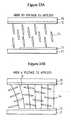
- Figs. 1A and 1Bare diagrams for explaining the structure and principles of operation of a panel of the TN LCD.
- an alignment filmis placed on transparent electrodes 12 and 13 formed on glass substrates, a rubbing treatment is performed so that orientation directions of the liquid crystalline molecules on the two substrates are shifted by 90° to each other, and a TN liquid crystal is sandwiched between the transparent electrodes. Due to the properties of the liquid crystal, liquid crystalline molecules in contact with the alignment films are aligned in the directions of the orientation defined by the alignment films. The other liquid crystalline molecules are aligned in line with the aligned molecules. Consequently, as shown in Fig. 1A , the liquid crystalline molecules are aligned while twisted by 90°.
- Two sheet polarizers 11 and 15are located in parallel with the directions of the orientation defined by the alignment films.
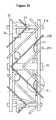
- Figs. 2A to 2Care diagrams for explaining this problem.
- Fig. 2Ashows a state of white display in which no voltage is applied
- Fig. 2Bshows a state of halftone display in which an intermediate voltage is applied
- Fig. 2Cshows a state of black display in which a predetermined voltage is applied. As shown in Fig.
- FIG. 2Ain the state in which no voltage is applied, liquid crystalline molecules are aligned in the same direction with a slight inclination (about 1° to 5°). In reality, the molecules are twisted as shown in Fig. 1A . For convenience' sake, the molecules are illustrated like Fig. 2A . In this state, light is seen nearly white in any azimuth. Moreover, as shown in Fig. 2C , in the state in which a voltage is applied, intermediate liquid crystalline molecules except those located near the alignment films are aligned in a vertical direction. Incident linearly-polarized light is therefore seen black but not twisted.
- Figs. 3A to 3Dare diagrams for explaining the IPS LCD.
- Fig. 3Ais a side view of the LCD with no voltage applied
- Fig. 3Bis a top view thereof with no voltage applied
- Fig. 3Cis a side view thereof with a voltage applied
- Fig. 3Dis a top view with a voltage applied.
- Figs. 3Ais a side view of the LCD with no voltage applied
- Fig. 3Bis a top view thereof with no voltage applied
- Fig. 3Cis a side view thereof with a voltage applied
- Fig. 3Dis a top view with a voltage applied.
- the IPS modeas shown in Figs.
- slit-like electrodes 18 and 19are formed in one substrate 17, and liquid crystalline molecules existent in a gap between the slit-like electrodes are driven with electric fields induced by a transverse electric wave.
- a material exhibiting positive dielectric anisotropyis used to make a liquid crystal 14.
- an alignment filmis rubbed in order to align the liquid crystalline molecules homogeneously so that the major axes of the liquid crystalline molecules will be nearly parallel to the longitudinal direction of the electrodes 18 and 19.
- the liquid crystalline moleculesare homogeneously aligned with an azimuth of 15° relative to the longitudinal direction of the slit-like electrodes in order to make a direction (direction of turn), to which the orientation of the liquid crystal is changed with application of a voltage, constant.
- a voltageis applied to the slit-like electrodes, as shown in Fig. 3C , liquid crystalline molecules existent near the slit-like electrodes change their orientation so that the major axes thereof will be turned 90° relative to the longitudinal direction of the slit-like electrodes.
- liquid crystalline molecules near the substrate 16are aligned so that the major axes thereof will be nearly parallel to the longitudinal direction of the electrodes 18 and 19.
- the liquid crystalline moleculesare therefore aligned while twisted from the upper substrate 16 to the lower substrate 17.
- the sheet polarizers 11 and 15are placed on and under the substrates 16 and 17 respectively so that the axes of transmission thereof will be orthogonal to each other.
- black displaycan be attained with no voltage applied, and white display canbe attained with a voltage applied.
- the IPS modeis characterized in that the liquid crystalline molecules do not erect themselves but turned in a transverse direction.
- the birefringent property of the liquid crystalvaries depending on a direction of an viewing angle and a problem occurs.
- the birefringent propertyhardly varies depending on a direction. This results in very good viewing angle characteristics.
- the IPS modehas another problems. One of the problems is that a response speed is quite low.
- the reason why the response speed is lowis that although a gap between electrodes in the normal TN mode in which liquid crystalline molecules are turned is 5 micrometers, the gap in the IPS mode is 10 micrometers or more.
- the response speedcan be raised by narrowing the gap between the electrodes.
- electric fields of opposite polaritiesmust be applied to the adjoining electrodes in the IPS mode, when the gap between the electrodes is narrowed, a short circuit occurs to bring about a display defect. For this reason, the gap between the electrodes cannot be narrowed very much.
- the ratio in area of the electrodes to displaygets large. This poses a problem that a transmittance cannot be improved.
- the IPS modesuffers from slow switching.
- drawbacksincluding a drawback that an image streams take place.
- the alignment filmis not rubbed parallel to the electrodes but rubbed in a direction shifted by about 15°.
- the alignment filmis not rubbed parallel to the electrodes but rubbed in a direction shifted by about 15°.
- the alignment filmis not rubbed parallel to the electrodes but rubbed in a direction shifted by about 15°.
- liquid crystalline moleculesare arrayed freely leftward or rightward and cannot be aligned in a predetermined direction. Rubbing is therefore carried out for rubbing the surface of the alignment film in a certain direction so that the liquid crystalline molecules will be aligned in the predetermined direction.
- Fig. 4is a diagram giving a definition of a coordinate system employed in studying viewing of a liquid crystal display (of the IPS type herein). As illustrated, a polar angle ⁇ and azimuth ⁇ are defined in relation to substrates 16 and 17, electrodes 18 and 19, and a liquid crystalline molecule 4.
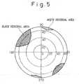
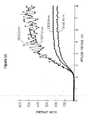
- Fig. 5is a diagram showing a gray-scale reversal characteristic of a panel concerning a viewing angle. A gray scale from white to black is segmented into eight gray-scale levels. Domain areas causing gray-scale reversal when a change in luminance is examined by varying the polar angle ⁇ and azimuth ⁇ are shown in Fig. 5 . In the drawing, reversal occurs at four hatched areas. Figs.
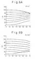
- FIGS. 6A and 6Bare diagrams showing examples of changes in luminance of display of 8 gray-scale levels in relation to the polar angle ⁇ with the azimuths fixed to values of 75° and 135° causing reversal.
- White gray-scale reversaloccurs at gray-scale levels associated with high luminances, that is, when white luminance deteriorates with an increasing value of the polar angle ⁇ .
- Black gray-scale reversaloccurs when black luminance increases with an increasing value of the polar angle ⁇ .
- the IPS modehas a problem that gray-scale reversal occurs in four azimuths.
- the IPS modehas a problem that it is harder to manufacture the IPS LCD than the TN LCD.
- any of the other characteristicssuch as a transmittance, a response speed and productivity, is sacrificed for the viewing angle characteristic.
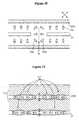
- Figs. 7A to 7Care diagrams for explaining the VA mode.
- the VA modeis a mode using a negative liquid crystal material and vertical alignment film.
- Fig. 7Awhen no voltage is applied, liquid crystalline molecules are aligned in a vertical direction and black display appears.
- Fig. 7Cwhen a predetermined voltage is applied, the liquid crystalline molecules are aligned in a horizontal direction and white display appears.
- the contrast in display offered by the VA modeis higher than that offered by the TN mode.
- the response speed at black levelis also higher.
- the VA modeis therefore attracting attention as a novel mode for a liquid crystal display.
- the VA modehas the same problem as the TN mode concerning halftone display, that is, a problem that the display state varies depending on the viewing angle.
- a voltage lower than a voltage to be applied for white displayis applied.
- liquid crystalline moleculesare aligned in an oblique direction. As illustrated, the liquid crystalline molecules are aligned parallel to light propagating from right below point to left above. The liquid crystal is therefore seen black when viewed from the left side thereof because a birefringent effect is hardly exerted on the left side thereof. By contrast, the liquid crystalline molecules are aligned vertically to light propagating from left below to right above.
- the liquid crystalexerts a great birefringent effect relative to incident light, therefore, display becomes nearly white.
- the VA modeprovides a much higher contrast than the TN mode and is superior to the TN mode in terms of a viewing angle characteristic, because even when no voltage is applied, liquid crystalline molecules near an alignment film are aligned nearly vertically.
- the VA modeis not certainly superior to the IPS mode in terms of the viewing angle characteristic.
- the viewing angle performance of a liquid crystal display device (LCD) in the TN modecan be improved by setting the orientation directions of the liquid crystalline molecules inside pixels to a plurality of mutually different directions.
- the orientation direction of the liquid crystalline moleculespre-tilt angles
- the rubbing treatmentis a processing which rubs the surface of the alignment film in one direction by a cloth such as rayon, and the liquid crystalline molecules are orientated in the rubbing direction. Therefore, viewing angle performance can be improved by making the rubbing direction different inside the pixels.
- Figs. 8A to 8Cshow a method of making the rubbing direction different inside the pixels.
- an alignment film 22is formed on a glass substrate 16 (whose electrodes, etc., are omitted from the drawing). This alignment film 22 is then bought into contact with a rotating rubbing roll 201 to execute the rubbing treatment in one direction.
- a photo-resistis applied to the alignment film 22 and a predetermined pattern is exposed and developed by photolithography.
- a layer 202 of the photo-resist which is patternedis formed as shown in the drawing.
- the alignment film 22is brought into contact with a rubbing roll 201 that is rotating to the opposite direction to the above so that only the open portions of the pattern are rubbed.
- the rubbing treatmentcan be done in arbitrarily different directions when the alignment film 22 is rotated relative to the rubbing roll 201.
- the rubbing treatmenthas gained a wide application, it is a treatment that rubs, and consequently damages, the surface of the alignment film and involves the problem that dust is likely to occur.
- a method which forms a concavo-convex pattern on an electrodeis known as another method of restricting the pre-tilt angle of the liquid crystalline molecules in the TN mode.
- the liquid crystalline molecules in the proximity of the electrodesare orientated along the surface having the concavo-convex pattern.
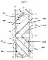
- Figs. 9A to 9Care diagrams for explaining the principles of the present invention.
- a domain regulating meansis included for regulating the orientation of a liquid crystal in which liquid crystalline molecules are aligned obliquely when a voltage is applied so that the orientation will include a plurality of directions within each pixel.
- electrodes 12 on an upper substrateare slitted and associated with pixels, and an electrode 13 on a lower substrate is provided with protrusions (projections) 20.
- liquid crystalline moleculesare aligned vertically to the surfaces of the substrates.
- an intermediate voltageis applied, as shown in Fig. 9B , electric fields oblique to the surfaces of the substrates are produced near the slits of the electrodes (edges of the electrodes).
- liquid crystalline molecules near the protrusions 20slightly tilt relative to their state attained with no voltage applied.
- the inclined surfaces of the protrusions and the oblique electric fieldsdetermine the directions in which the liquid crystalline molecules are tilted.
- the orientation of the liquid crystalis divided into different directions along a plane defined by each pair of protrusions 20 and the center of each slit. At this time, for example, light transmitted from immediately below to immediately above is affected by weak birefringence because the liquid crystalline molecules are slightly tilting.
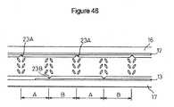
- Figs. 10A to 10Care diagrams for explaining determination of an orientation by protrusions of dielectric material provided on the electrodes.
- the dielectric materialsare insulating materials of low dielectric constant. Referring to Figs. 10A to 10C , an orientation determined by the protrusions will be discussed.
- Protrusionsare formed alternately on the electrodes 12 and 13, and coated with the vertical alignment films 22.
- a liquid crystal employedis of a negative type.
- the vertical alignment films 22cause the liquid crystalline molecules to align vertically to the surfaces of the substrates. In this case, rubbing need not be performed on the vertical alignment films.
- Liquid crystalline molecules near the protrusions 20try to align vertically to the inclined surfaces of the protrusions. The liquid crystalline molecules near the protrusions are therefore tilted.
- liquid crystalline molecules near the protrusionsare therefore tilted.
- liquid crystalline moleculesare aligned nearly vertically to the surfaces of the substrates. Consequently, as shown in Fig. 9A , excellent black display can appear.
- the distribution of electric potentials in the liquid-crystal layeris as shown in Figs. 10B and 10C .
- the distributionIn the regions of the liquid-crystal layer without the protrusions, the distribution is parallel to the substrates (electric fields are vertical to the substrates). However, the distribution is inclined near the protrusions.
- a voltageis applied, as shown in Figs. 7B and 7C , the liquid crystalline molecules tilt according to an electric field strength. Since the electric fields are vertical to the substrates, when a direction of tilt is not defined by carrying out rubbing, the azimuth in which the liquid crystalline molecules tilt due to the electric fields includes all directions of 360°. If there are pre-tilted liquid crystalline molecules as shown in Fig.
- the protrusionsfill the role of a trigger for determining azimuths in which the liquid crystalline molecules are aligned with application of a voltage.
- the protrusionsneed not have inclined surfaces (slopes) of large area. For example, the inclined surfaces over the whole pixel are unnecessary. However, if the size of the inclined surfaces is too small, the effect of the slope and electric field are not available. Therefore, the width of the inclined surfaces are required to be determined according to the materials and shape of the protrusions. A good result is obtained when the width of the protrusions is 5 ⁇ m. This means that when the width of the protrusions is larger than 5 ⁇ m, a good result can be certainly obtained.
- the side surfacesare almost vertical to the substrates. These side surfaces also operate as the domain regulating means. Therefore, the surfaces vertical to the substrates are included in the inclined surfaces.
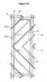
- Fig. 11shows the orientation direction when protrusions are used as the domain regulating means.
- Fig. 11Ashows a bank having two slopes and the liquid crystalline molecules are oriented in two directions different from each other at an angle of 180 degrees with the bank being the boundary.
- Fig. 11Bshows a pyramid and the liquid crystalline molecules are oriented in four directions different from one another at an angle of 90 degrees with the apex of the pyramid being the boundary.
- Fig. 11Cshows a hemisphere and the orientation of the liquid crystalline molecules assumes symmetry of rotation with the axis of the hemisphere perpendicular to the substrate being the center. In the case of Fig.
- the display statebecomes the same for all the viewing angles.
- a larger number of domains or directionsis better.
- the oblique orientation of the liquid crystalbecomes rotationally symmetrical, there arises a problem that light use efficiency deteriorates. This is because when domains in the liquid crystal are defined uninterruptedly and radially, liquid crystalline molecules lying along a transmission axis and absorption axis of the sheet polarizer work inefficiently, and liquid crystalline molecules lying in directions of 45° with respect to the axes work most efficiently.
- the directions included in the oblique orientation of the liquid crystalare mainly four directions or less.
- the ratio in number of liquid crystalline molecules aligned in directions in which light components to be projected on the display surface propagate with azimuth mutually different by 180°should preferably be nearly even.
- the ratio in number of aligned liquid crystalline molecules of one setis nearly even, while the ratio in number of aligned liquid crystalline molecules of the other set is uneven.
- the set of aligned liquid crystalline molecules of which ratio in number is nearly evenis a majority, and the set of aligned liquid crystalline molecules of which ratio in number is uneven may be negligible. In other words, a characteristic analogous to that exhibited when two domains are defined in 180° different directions can be realized.
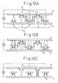
- Figs. 9A to 9Cfor realizing the domain regulating means, the electrodes 12 on the upper substrate are slitted and associated with pixels, and the electrode 13 on the lower substrate is provided with the protrusions 20. Any other means will also do.
- Figs. 12A to 12Care diagrams showing examples of realizing the domain regulating means.
- Fig. 12Ashows an example of realizing it by devising the shapes of the electrodes
- Fig. 12Bshows an example of devising the contours of the surfaces of the substrates
- Fig. 12Cshows an example of devising the shapes of the electrodes and the contours of the surfaces of the substrates.
- the orientations shown in Fig. 8can be attained.
- the structures of liquid crystalsare a bit different from one another.
- ITO electrodes 41 and 42 on both substrates or one of the substratesare slitted.
- the surfaces of the substratesare processed for vertical alignment, and a negative liquid crystal is sealed in.
- liquid crystalline moleculesare aligned vertically to the surfaces of the substrates.
- electric fieldsare generated obliquely to the surfaces of the substrates near the slits (edges) of the electrodes.
- the oblique electric fieldsthe directions in which liquid crystalline molecules are tilted are determined.
- the orientation of the liquid crystalis divided as illustrated into right and left directions.
- the oblique electric fields induced near the edges of the electrodesare used to align the liquid crystalline molecules rightward and leftward. This technique shall therefore be referred to as an oblique electric field technique.
- protrusions 20are formed on both the substrates.
- the surfaces of the substratesare processed for vertical alignment, and a negative liquid crystal is sealed in.
- the liquid crystalline moleculesare aligned vertically to the surfaces of the substrates in principle.
- the liquid crystalline moleculesare aligned at a little tilt.
- the liquid crystalline moleculesare aligned in the directions of tilt.
- the electric fieldsare interrupted (state close to the state attained by the oblique electric field technique, the same state as the state attained by the structure having the electrodes slitted). More stable orientation division can be achieved.
- This techniqueshall be referred to as a both-side protrusion technique.
- Fig. 12Cshows an example of combining the techniques shown in Figs. 12A and 12B . The description will be omitted.
- the portions of the electrodes formed as the slits in Fig. 12Amay be dented, and the dents may be provided with inclined surfaces.
- protrusionsmay be formed on the substrates, and ITO electrodes may be formed on the substrates and protrusions.
- the electrodes having the protrusionsmay be realized. Even this structure can regulate the orientation of the liquid crystal.
- dentsmay be substituted for the protrusions.
- any of the described domain regulating meansmay be formed on one of the substrates.
- any pair of domain regulating meanscan be employed.
- the protrusions or dentsshould preferably be designed to have inclined surfaces, the protrusions or dents having vertical surfaces can also exert an effect of a certain level.
- protrusions, dents, or slitscan be formed like a unidirectional lattice with a predetermined pitch among them.
- the protrusions, dents, or slitsare a plurality of protrusions, dents, or slits bent at intervals of a predetermined cycle, orientation division can be achieved more stably.
- the protrusions, dents, or slitsare located on both substrates, they should preferably be arranged to be offset by a half pitch.
- the size of domain areascan be optionally determined because the domain regulating means are provided on both of the pixel electrode and counter electrode. Further, at least one of the domain regulating means has inclined surfaces, the response speed can be improved,
- protrusions or dentsmay be formed like a two-dimensional lattice.
- protrusions or dentsmay be arranged to be opposed to the centers of squares of the two-dimensional lattice.
- orientation divisionoccurs within each pixel.
- the pitch of the protrusions, dents, or slitsmust be smaller than that of pixels.
- the results of examining the characteristics of an LCDdemonstrate that a viewing angle characteristic is quite excellent and equal to or greater than those of not only a TN LCD but also an IPS LCD. Even when the LCD is viewed from its front side, the viewing angle characteristic is quite excellent, and the contrast ratio is 400 or more (twice as high as that offered by the TN LCD).
- the transmittance offered by the TN LCDis 30 %
- the one offered by the IPS LCDis 20 %
- the one offered by the present designis 25 %.
- the transmittance offered by the present designis lower than the one offered by the TN LCD but higher than the one offered by the IPS LCD. A response speed is outstandingly higher than those offered by the other modes.
- a TN LCD panelexhibits an on speed (for transition from 0 V to 5 V) of 23 ms, an off speed (for transition from 5 V to 0 V) of 21 ms, and a response speed (on + off) of 44 ms
- an IPS LCD panelexhibits an on speed of 42 ms, an off speed of 22 ms, and a response speed of 64 ms.
- the on speedis 9 ms
- the off speedis 6 ms
- the response speedis 15 ms.
- the response speedis 2.8 times higher than the one offered by the TN mode and 4 times higher than the one offered by the IPS mode, and is a speed causing no problem in display of a motion picture.
- a rubbing stepis a step likely to produce the largest amount of refuse. After the completion of rubbing, substrates must be cleaned (with running water or IPA) without fail. The cleaning may damage an alignment film, causing imperfect alignment. By contrast, according to the present invention, since the rubbing step is unnecessary, the step of cleaning substrates is unnecessary.
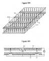
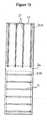
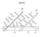
- Fig. 13is a diagram showing the overall configuration of a liquid crystal panel of the first design of a liquid crystal display device.
- the liquid crystal panel of the first design of a liquid crystal display deviceis a TFT LCD.
- a common electrode 12is formed on one glass substrate 16.
- the other glass substrate 17is provided with a plurality of scan bus lines 31 formed parallel to one another, a plurality of data bus lines 32 formed parallel to one another vertically to the scan bus lines, and TFTs 33 and cell electrodes 13 formed like a matrix at intersections between the scan bus lines and data bus lines.
- the surfaces of the substratesare processed for vertical alignment.
- a negative liquid crystalis sealed in between the two substrates.
- the glass substrate 16is referred to as a color filter (CF) substrate because color filters are formed, while the glass substrate 17 is referred to as a TFT substrate.
- CFcolor filter
- TFT substrateTFT substrate
- Figs. 14A and 14Bare diagrams showing the structure of a panel in accordance with the first design of a liquid crystal display device.
- Fig. 14Ais a diagram illustratively showing a state in which the panel is seen obliquely
- Fig. 14Bis a side view of the panel.
- Fig. 15is a diagram showing the relationship between a pattern of protrusions and pixels in the first design of a liquid crystal display device
- Fig. 16is a diagram showing the pattern of protrusions outside a display area of a liquid crystal panel of the first design of a liquid crystal display device
- Fig. 17is a sectional view of the liquid crystal panel of the first design of a liquid crystal display device.
- a black matrix layer 34, an ITO film 12 providing color filters and a common electrode, and protrusions 20 parallel to one another with an equal pitch among themare formed on the surface of a side of a CF substrate 16 facing, a liquid crystal.
- the ITO film and protrusionsare coated with a vertical alignment film that is omitted therein.
- Gate electrodes 31 forming gate bus lines, CS electrodes 35, insulating films 40 and 43, electrodes forming data bus lines, an ITO film 13 providing pixel electrodes, and protrusions parallel to one another with an equal pitch among themare formed on the surface of a side of a TFT substrate 17 facing the liquid crystal.
- the TFT substrateis further coated with a vertical alignment film, though the vertical alignment film is omitted from the figure.
- Reference numerals 41 and 42denote a source and drain of a TFT.
- protrusions 20A and 20Bare made of a TFT flattening material (positive resist).
- the pattern of the protrusions 20A and 20Bis a pattern of parallel protrusions extending straightly and arranged with an equal pitch among them.
- the protrusions 20A and 20Bare arranged to be offset by a half pitch.
- the structure shown in Fig. 14Bis thus realized.
- the orientation of the liquid crystalis divided into two directions to thus divide each domain into two regions.
- Fig. 15The relationship of the pattern of protrusions to pixels is shown in Fig. 15 .
- Fig. 15in a general color-display liquid crystal display, three pixels of red, green, and blue constitute one color pixel.
- the width of each of the red, green, and blue pixelsis approximately one-third of the length thereof so that color pixels can be arrayed with the same gap kept above and below them.
- a pixeldefines each pixel electrode.
- gate bus lineshidden behind the protrusions 20B
- data bus lines 32are laid down lengthwise.
- the TFTs 33are located near intersections between the gate bus lines 31 and data bus lines 32, whereby the pixel electrodes are interconnected.
- each pixelis divided into an upper part 13A and lower part 13B.
- each of the pixels 13A and 13Bthree protrusions 20A are lying and four protrusions 20B are lying.
- Three first regions each having the protrusions 20B on the upper side of the panel and the protrusions 20A on the lower side thereof, and three second regions each having the protrusions 20A on the upper side thereof and the protrusions 20B on the lower side thereofare defined in one pixel composed of the pixels 13A and 13B.
- a total of six regions of the first and second regionsare defined.
- the pattern of the protrusions 20A and 20Bis extending outside the topmost pixels and beyond the rightmost pixels. This is intended to allow orientation division to occur in the outermost pixels in the same manner as that in the inner pixels.
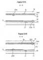
- Figs. 18A and 18Bare diagrams showing the structure of a panel in the fifth design of a liquid crystal display device.
- Fig. 18Ais a diagram illustratively showing a state in which the panel is seen obliquely
- Fig. 18Bis a side view.
- the fifth design of a liquid crystal display deviceis an example in which the structure of a panel corresponds to the structure shown in Fig. 12C .
- the protrusions 20Aare created as illustrated on the electrode 12 (herein, a common electrode) formed on the surface of one substrate by applying a positive resist, and the slits 21 are created in the electrodes 13 (herein, cell (pixel) electrodes) formed on the surface of the other substrate.
- the liquid crystal display device of the VA system and, particularly, the VA system equipped with a domain regulating meansfeatures a high display quality as described above but becomes expensive due to the provision of the domain regulating means and, hence, it has been desired to further decrease the cost.
- the photoresist that is appliedmust be exposed to light through a pattern followed by developing and etching, requiring an increased number of steps and increased cost, deteriorating the yield.
- the pixel electrodemust be formed by patterning, and the number of the steps does not increase despite a pixel electrode having a slit is formed.
- the costcan be decreased when the domain regulating means is formed by slits rather than protrusions.
- the opposing electrode of the color filter substrate (CF substrate)is usually a flat electrode. When a slit is to be formed in the opposing electrode, an etching step must be executed after the patterned photoresist is developed.
- the developed photoresistcan be used in its form without much driving up the cost of forming the protrusion.
- the domain regulating means on the side of the TFT substrateis formed by a slit in the pixel electrode and the domain regulating means on the side of the color filter substrate is formed by a protrusion, driving up the cost little.
- Fig. 19is a diagram showing a pattern of slits of each pixel electrode in a modification of the fifth design of a liquid crystal display device. This modification corresponds to an example in which the protrusions 20B are replaced with the slits 21 in the third design of a liquid crystal display device.
- the electric connection portionsare formed in the perimeter of the pixel electrode 13 and are shielded by the black matrices (BM) 34 to obtain luminance and response speed comparable with those of when protrusions are formed on both of them.
- BMblack matrices
- the pixelis divided into upper and lower two portions.
- Reference numeral 34Adenotes an opening of the upper side defined by BM
- 34Bdenotes an opening of the lower side defined by BM, and light passes through the inside of the openings.
- the bus linessuch as gate bus lines 31 and data bus lines 32 are made of a metal material and have light-shielding property.
- the pixel electrodesmust be so formed as will not be superposed on the bus lines, and light must be shielded between the pixel electrodes and the bus lines.
- the BM 34has heretofore been provided for shielding light for these portions.
- the electric connection portionsare provided in the perimeter of the pixel, and light is shielded by the BM 34. There is no need to newly provide the BM for shielding light for the electric connection portions; i.e., the conventional BM may be used or the BM may be slightly expanded without decreasing the numerical aperture to a serious degree.
- the panel of the fifth design of a liquid crystal display deviceis of a type in which each pixel is divided into two portions, and therefore basically exhibits the same characteristics as the one of the first design of a liquid crystal display device.
- the viewing angle characteristic of the panelbecomes identical to that of the panel of the second design of a liquid crystal display device when the phase-difference film or optical compensation film is employed.
- the response speed of the panelis slightly lower than that of the panel of the first design of a liquid crystal display device, because oblique electric fields induced by the slits formed in one substrates are utilized. Nevertheless, the on speed is 8 ms, the off speed is 9 ms, and the switching speed is 17 ms. Thus, the response speed is much higher than the ones offered by the conventional modes.
- the manufacturing processis simpler than those of the first and second design of a liquid crystal display devices.
- the electrodesare slitted. A pattern of protrusions is then drawn on a common electrode using a photo-resist. As already described, the rubbing step is unnecessary, and the associated after-rubbing cleaning step can therefore be omitted.
- the measurement results of an example in which slits are provided an the cell (pixel) electrode and no slit is provided on the counter electrodeis described.
- the cell electrodeshave the slits, and the width and pitch of the slits are determined properly.
- stable alignmentis attained, that is, liquid crystalline molecules are aligned in all azimuths of 360° inside walls defined with oblique electric fields induced near the slits.
- the liquid crystalline moleculesare aligned in all azimuths of 360° within each small region.
- the viewing angle characteristic of the panelis therefore excellent. An image that is seen homogeneous in all azimuths of 360° can be produced. However, a response speed has not been improved.
- the on speedis 42 ms
- the off speedis 15 ms.
- a switching speed that is a sum of the on and off speedsis 57 ms.
- the response speedhas not been improved very much. This means that no problem occurs in displaying a still image but the response speed is not high enough to display a motion picture like the one offered by the IPS mode. If the number of slits is decreased, the response speed is further decreased. This is presumably that when the number of the slits is decreased, the area of each domain becomes large, and it lengthens a time in which all liquid crystalline molecules are oriented.
- Fig. 20is a diagram illustrating the distribution of orientation of liquid crystalline molecules in the electric connection portions.
- the liquid crystalline moleculesare oriented in a direction perpendicular to the direction in which the protrusion and the slit extend as viewed from the upper side.
- the electric connection portionhowever, the liquid crystalline molecules 14a are oriented in different directions, developing abnormal orientation. Therefore, as shown in Fig.
- liquid crystalline molecules in the spaces between the protrusions 20A and the slits 21 of the electrodesare aligned in a direction vertical (vertical direction in the drawing) to the protrusions 20A and slits 21.
- liquid crystalline moleculesare aligned in the horizontal direction but not in the vertical direction.
- Oblique electric fields induced by the slopes of the protrusions or the slitsenable control of the liquid crystal in the vertical direction in the drawing but cannot enable control in the lateral direction. For this reason, a random domain is produced sideways near the apices of the protrusions and the centers of the slits. This has been confirmed through microscopic observation.
- a domain near the apex of a protrusionis too small to be discerned, causing no problem.
- an area occupied by a domain having liquid crystalline molecules aligned sideways and lying near a slitis so large as to be discerned even by naked eyes.
- the domainis produced regularly, even if the domain is large, it will not be cared.
- an imageis seen irregular. This leads to deteriorated display quality.
- the panel in the fifth design of a liquid crystal display devicemakes a little poor impression on image quality compared with the one provided by the first design of a liquid crystal display device, though display has no problem.
- Abnormal orientationcauses the luminance of the panel and the response speed to decrease.
- a comparison of a practical device in which an electric connection portion is formed at the central portion of the pixel electrode with a practical device in which a protrusion is providedindicates abnormal conditions such as a drop in the luminance and a residual image in which white appears bright for a moment when black changes into white.
- this problemis solved.
- a panel of the sixth design of a liquid crystal display deviceis provided by modifying the shape of the protrusions 20A and that of the slits 21 in the cell electrodes 13 in the panel of the fifth design of a liquid crystal display device.
- Fig. 22is a diagram showing the shape of the protrusions 20A of the sixth design of a liquid crystal display device and that of the cell electrodes 13 thereof which are seen in a direction vertical to the panel. As illustrated, the protrusions 20A are zigzagged. Owing to this shape, as shown in Fig. 23 , a domain divided regularly into four regions is produced. Consequently, irregular display that poses a problem in the fifth design of a liquid crystal display device can be overcome.
- Fig. 24is a plan view of a pixel portion in the LCD according to a sixth design of a liquid crystal display device
- Fig. 25is a diagram illustrating a pattern of a pixel electrode according to the sixth design of a liquid crystal display device
- Fig. 26is a sectional view of a portion indicated by A-B in Fig. 24 .
- the glass substrate 16 on which the color filter 39 is formedis called color filter substrate (CF substrate).
- the scan bus lines 31form gate electrodes of the TFTs 33, and the data bus lines 32 form drain electrodes 42 of the TFTs 33.
- the sources 41are formed in the same layers as the data bus lines 32 and are formed simultaneously with the formation of the drain electrodes.
- a gate-insulating film, an amorphous silicon active layer and a channel protection filmare formed on predetermined portions between the scan bus line 31 and the data bus line 32, an insulating film is formed on the layer of the data bus line 32 and, besides, an ITO film corresponding to the pixel electrode 13 is formed thereon.
- the pixel electrode 13is of a rectangular shape of 1:3 as shown in Fig. 25 , and has a plurality of slits 21 in a direction tilted by 45 degrees with respect to the sides thereof. In order to stabilize the potential of every pixel electrode 13, furthermore, a CS electrode 35 is provided to form a storage capacitor.
- the glass substrate 17is called TFT substrate.
- the sequences of protrusions 20A of the CF substrate and the slits 21 of the TFT substratesare arranged being deviated by one-half pitch of their arrangement, so that the substrates maintain an inverse relationship.
- the protrusions and the slitsmaintain a positional relationship as shown in Fig. 12C , and the orientation of the liquid crystals is divided into four directions.
- the pixel electrode 13is formed by forming an ITO film, applying a photoresist thereon, exposing it to light through a pattern of electrode, followed by developing and etching.
- the slitcan be formed through the same step as the conventional step if the patterning is so effected as to remove the portion of the slit, without driving up the cost.
- the pixel electrode 13Upon forming the slits in the pixel electrode 13, the pixel electrode 13 is divided into a plurality of partial electrodes. Here, however, a signal of the same voltage must be applied to the partial electrodes and, hence, the partial electrodes must be electrically connected together. According to this design of a liquid crystal display device as shown in Fig. 25 , therefore, the pixel electrode 13 is not completely divided by slits, but the electrode is left at the perimetric portions 131, 132, 133 of the pixel electrode 13 to form electric connection portions. As described above, the alignments of the molecules are disturbed near the electric connection portions. Therefore, according to this design of a liquid crystal display device as shown in Fig.
- the electric connection portionsare formed in the perimeter of the pixel electrode 13 and are shielded by the BM 34 to obtain luminance and response speed comparable with those of when protrusions are formed on both of them.
- the pixelis divided into upper and lower two portions.
- Reference numeral 34Adenotes an opening of the upper side defined by BM
- 34Bdenotes an opening of the lower side defined by BM, and light passes through the inside of the openings.
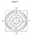
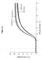
- Figs. 27 to 28Care diagrams showing a viewing angle characteristic exhibited by the sixth design of a liquid crystal display device. As illustrated, the viewing angle characteristic is excellent and irregular display is overcome. Moreover, a response speed is as high as a switching speed is 17.7 ms. Thus, very fast switching can be achieved.
- Figs. 29A and 29Billustrate another example of the pattern of the pixel electrode, wherein the BM 34 shown in Fig. 29B is formed on the pixel electrode 13 shown in Fig. 29A .
- the pattern of the pixel electrodecan be modified in a variety of ways. For example, electric connection portions may be formed in the perimeter on both sides of the slit to decrease the resistance between the partial electrodes.
- slitscan be provided in the place of the protrusions on the counter electrode 12. Namely, both of the domain regulating means are realized by the slits. However, in this constitution, the response speed is decreased.
- the electric connection portionsare formed in the same layer as the partial electrodes.
- the electric connection portionsmay be formed in a separate layer.
- a seventh design of a liquid crystal display devicedeals with this case.
- Figs. 30A and 30Bare diagrams illustrating a pattern and a structure of the pixel electrode according to the seventh design of a liquid crystal display device.
- the seventh design of a liquid crystal display deviceis the same as the sixth design of a liquid crystal display device except that the connection electrode 134 is formed simultaneously with the formation of the data bus line 32, and a contact hole is formed in the insulating layer 135 to connect the partial electrode 13 to the connection electrode 134.
- the connection electrode 134is formed simultaneously with the data bus line 32.
- the connection electrode 134may be formed simultaneously with the gate bus line 31 or the CS electrode 35.
- the connection electrodemay be formed separately from the formation of the bus line. In this case, however, a step must be newly provided for forming the connection electrode, i.e., a new step must be added. In order to simplify the steps, it is desired to form the connection electrode simultaneously with the formation of the bus line or the CS electrode.
- connection electrode which becomes a cause of abnormal orientationis more separated away from the liquid crystal layer than that of the sixth design of a liquid crystal display device, making it possible to further decrease abnormal orientation.
- connection electrodeis formed of a light-shielding material, such a portion is shielded from light, and the quality of display is further improved.
- Fig. 31is a plan view of a pixel portion according to an eighth design of a liquid crystal display device
- Fig. 32is a sectional view of a portion A-B in Fig. 31
- the eighth design of a liquid crystal display deviceis the same as the sixth design of a liquid crystal display device except that a protrusion 20C is formed in the slit of the pixel electrode 13. Both the slit of the electrode and the insulating protrusion formed on the electrode define the orientation region of the liquid crystals.
- the protrusion 20Cis formed in the slit 21 as in this design of a liquid crystal display device, the directions of orientation of the liquid crystals due to the slit 21 and the protrusion 20C are in agreement, the protrusion 20C assisting the division of orientation by the slit 21, to improve stability. Therefore, the orientation is more stabilized and the response speed is more increased than those of the first design of a liquid crystal display device.
- the protrusion 20Cis formed by laminating the layers that are formed when the CS electrode 35, gate bus line 31 and data bus line 32 are formed.
- Figs. 33A to 33Jare diagrams illustrating a process for producing a TFT substrate according to the eighth design of a liquid crystal display device.
- a metal film of the gate layeris formed on a glass substrate 17.
- Fig. 33Bportions corresponding to gate bus lines 31, CS electrodes 35 and protrusions 312 are left relying upon the photolithography method.
- Fig. 33Ca gate-insulating film, an amorphous silicon active layer and a channel protection film are continuously formed.
- the channel protection film 314is left in a self-aligned manner by exposure to light through the back surface.
- Fig. 33Aa metal film of the gate layer is formed on a glass substrate 17.
- Fig. 33Bportions corresponding to gate bus lines 31, CS electrodes 35 and protrusions 312 are left relying upon the photolithography method.
- Fig. 33Ca gate-insulating film, an amorphous silicon active layer and a channel protection film are continuously formed.
- a metal film 321is formed for forming the contact layer and the source-drain layer.
- a source electrode 41 and a drain electrode 42are formed relying on the photolithography method. At this moment, the metal film is left even at a position corresponding to the protrusion 20C on the inside of the slit.
- a passivation film 33is formed.
- a contact hole 332is formed for the source electrode 41 and the pixel electrode.
- an ITO film 341is formed.
- a pixel electrode 13is formed by the photolithography method. Slits are formed at this moment.
- the protrusion 20Cis formed in the slit 21 of the pixel electrode 13 without, however, increasing the number of the steps compared with the conventional process. Besides, the orientation is further stabilized owing to the protrusion 20C.
- the protrusion in the slit of the pixel electrodeis formed by superposing three layers, i.e., gate bus line layer, channel protection layer and source/drain layer. The protrusion, however, may be formed by one layer or by a combination of two layers.
- Fig. 34is a diagram showing the shape of the protrusions 20A and 20B in the ninth design of a liquid crystal display device which are seen in a direction vertical to the panel.
- Fig. 35is a diagram showing a practical plan view of pixel portions of the ninth design of a liquid crystal display device.
- a panel of the ninth design of a liquid crystal display deviceis provided by zigzagging the protrusions 20A and 20B in the panel of the first design of a liquid crystal display device like those in the one of the sixth design of a liquid crystal display device.
- the protrusions 20A and 20Bare zigzagged so that an orientation causing each domain to be divided into four regions can be attained.
- the response speed of the panelis identical to that of the panel of the first design of a liquid crystal display device.
- the viewing angle characteristic thereofis identical to the one in the sixth design of a liquid crystal display device, and is so excellent as to demonstrate that the orientation is divided vertically and laterally uniformly.
- Optimal values of the width, height and gap of the protrusionshave relations to each other.
- the direction of tilt of liquid crystalline moleculescan be controlled to include four directions.
- Regions A, B, C, and D in Fig. 34are regions to be controlled so that liquid crystalline molecules therein will be aligned in the four directions.
- the ratio of the regions within one pixelis uneven. This is because the pattern of protrusions is continuous and is located in the same way in all pixels, and a pitch of repeated patterns of protrusions is matched with a pitch of arrayed pixels.
- the viewing angle characteristic shown in Fig. 27 to 28Cis exhibited but does not reflect the uneven ratio of regions resulting from orientation division. However, this state is not very preferable.
- the width of a resistis 7 micrometers, an interval between resist lines is 15 micrometers, the height of the resist is 1.1 micrometers, and the thickness of cells is 3.5 micrometers.
- a liquid crystal display of size 15was produced as a prototype. Some resist lines interfered with gate bus lines and data bus lines. Nevertheless, generally good display appeared. Even when the width of the resist was increased to be 15 micrometers and the interval between resist lines was increased to 30 micrometers, nearly the same results were obtained.
- the pitch of repeated patterns of protrusions or dentsshould be set to an integral submultiple or multiple of the pitch of pixels.
- a cycle of protrusionsmust be designed in consideration of a cycle of pixels and should preferably be set to an integral submultiple or multiple of the pitch of pixels.
- the ratio of regions within one pixel in which liquid crystalline molecules are aligned in four different directionsis even.
- the pitch of repeated patterns of protrusionsshould be matched with the pitch of arrayed pixels, and a continuous pattern of protrusions should be adopted.
- the protrusions of dielectric materialsare formed in a zig-zag manner on the electrodes 12, 13 as the domain regulating means and the protrusions regulate the alignment direction of the liquid crystalline molecules.
- the slits provided on the electrodesgenerate oblique electric fields, at the edges thereof, and the oblique electric fields operate as the domain regulating means.
- the edges of the cell (pixel) electrodesalso generate oblique electric field. Therefore, the oblique electric field must be considered as the domain regulating means.
- Figs. 37A and 37Bare diagrams for explaining this phenomenon and shows the case of the vertical orientation somewhat inclined from the vertical direction.
- each liquid crystal particle 14is oriented substantially vertically when no voltage is applied thereto.
- an electric fieldis generated in vertical direction in the electrodes 12 and 13 in the region other than the perimeter of the electrode 13, so that the liquid crystalline molecules 14 are tilted in the direction perpendicular to the electric field.
- One electrodeis a common electrode, and the other electrode is a display pixel electrode separated into each display pixel. Therefore, as shown in Fig. 37B , the direction of the electric field 8 is inclined at its perimetric edge (edge).
- the liquid crystalline molecules 14are tilted in the direction perpendicular to the electric field 8.
- the direction of inclination of the liquid crystaltherefore, is different between the central portion and the edge of the pixel as shown. This phenomenon is called "reverse tilt".
- a reverse tiltcauses a schlieren structure to be formed in the display pixel area and thus deteriorates the display quality.
- Fig. 38is a diagram showing a portion 41 where the schlieren structure can be observed in a configuration formed with the zigzag protrusion pattern of the ninth design of a liquid crystal display device.
- Fig. 39is a diagram showing in enlarged form the neighborhood of the portion 41 where a schlieren structure is observed and also shows the direction in which the liquid crystalline molecules 14 are tilted upon application of a voltage thereto.
- protrusions of different materialsare formed on the pixel electrode substrate formed with a TFT and on the opposed substrate formed with a common electrode.
- a vertical alignment filmis printed, and the device is assembled without being rubbed.
- the cell thicknessis 3.5 ⁇ m.
- the portion 41 where the schlieren structure is observedis where the direction in which the liquid crystalline molecules are fallen by the orientation regulation force due to the diagonal electric field is considerably different from the direction of orientation regulation due to the protrusions. This reduces the contrast and the response rate, thereby leading to a deteriorated display quality.
- Fig. 40is a diagram showing a region appearing black in the pixel on the liquid crystal panel configured in the ninth design of a liquid crystal display device. In this region, the change in orientation is found to be very slow upon application of a voltage.
- Fig. 41Ais a sectional view taken in line A-A' in Fig. 40
- Fig. 41Bis a sectional view taken in line B-B'.
- the section A-A'has a region looking black in the neighborhood of the left edge, while the neighborhood of the right edge lacks a region appearing black. In correspondence with this, as shown in Fig.
- the direction in which the liquid crystalline molecules are tilted by the orientation regulation force due to the diagonal electric fieldis considerably different from the direction of orientation regulation due to the protrusions in the neighborhood of the left edge, while the direction in which the liquid crystalline molecules are tilted by the orientation regulation force due to the diagonal electric field comparatively coincides with the direction of orientation regulation due to the protrusions in the neighborhood of the right edge.
- a region looking blackis present in the neighborhood of the right edge but absent in the neighborhood of the left edge.
- the direction in which the liquid crystalline molecules are tilted by the orientation regulation force due to the diagonal electric fieldis considerably different from the direction of orientation regulation due to the protrusions in the neighborhood of the right edge, while the direction in which the liquid crystalline molecules are tilted by the orientation regulation force due to the diagonal electric field comparatively coincides with the direction of orientation regulation due to the protrusions in the neighborhood of the left edge.
- the deterioration of the display qualityis attributable to the portion where the direction in which the liquid crystalline molecules are tilted by the orientation regulation force due to the diagonal electric field at an edge of the display pixel electrode is considerably different from the orientation regulation force due to the protrusions upon application of a voltage thereto.
- the display qualityis seen to deteriorate in the neighborhood of the bus line (gate bus line or data bus line) in the pixel. This is due to the undesirable minute region (domain) formed in the neighborhood of the bus line and the resulting disturbance of liquid crystal orientation and reduced response rate.
- the problemthus is posed of a reduced viewing angle characteristic and a reduced color characteristic in half tone.
- Figs. 42A and 42Bare diagrams showing a fundamental configuration of a LCD according to a tenth design of a liquid crystal display device.
- a pixelfunctions within the range defined by a cell electrode 13, which will be called a display region and the remaining part a non-display region.
- a bus line and a TFTare arranged in a non-display region.
- a bus line made of a metal materialhas a masking characteristic but a TFT transmits light.
- BMblack matrix
- a protrusion 20Ais arranged in the non-display region on a common electrode 12 of a CF substrate 16 so as to generate an orientation regulation force in a direction different from the orientation restriction force exerted due to a diagonal electric field generated by an edge of the cell electrode 13.
- Fig. 42Ashows the state where no voltage is applied. In this state, liquid crystalline molecules 14 are oriented substantially perpendicular to the surfaces of the electrodes 12, 13 and the protrusion 20A due to the vertical orientation process. Upon application of a voltage thereto, as shown in Fig. 42B , the liquid crystalline molecules 14 are oriented in the direction perpendicular to the electric field 8.
- the electric fieldis formed diagonally from the neighborhood of an edge of the cell electrode 13 toward the non-display region. This diagonal electric field tends to orient the liquid crystalline molecules 14 in a direction different from the orientation in the display region as shown in Fig. 37B .
- the orientation regulation force of the protrusion 42orients the liquid crystalline molecules 14 in the same direction as in the display region, as shown in Fig. 42A .
- Fig. 43is a diagram showing a protrusion arrangement pattern in a liquid crystal display device of the tenth design of a liquid crystal display device.
- Fig. 44is a diagram showing, in enlarged form, the portion defined by a circle in Fig. 43 .
- a new protrusion 52is formed in the vicinity of the portion where a schlieren structure is observed. This protrusion 52 is connected to and integrally formed with a protrusion arrangement 20A formed on the common electrode 12. The relation shown in Figs.
- Fig. 62shows a modification in which the protrusion 52 is arranged to face the edge of the pixel electrode 13. In this modification, no schlieren structure is observed.
- the tenth design of a liquid crystal display devicewhich uses an acrylic transparent resin for the protrusion, can alternatively use a black material.
- the use of a black resin materialcan shield the leakage light at the protrusion and therefore improves the contrast. This is also the case with the designs of a liquid crystal display device described below.
- the protrusion 52which is formed as a non-display region domain regulating means in the non-display region as shown in Figs. 42A to 43 can be replaced by a depression (groove) with equal effect.
- the depressionis required to be formed on the TFT substrate.
- Any non-display domain regulating means which has an appropriate orientation regulation forcecan be employed.
- the direction of orientationis known to change, for example, when the light of a specific wavelength such as ultraviolet light is irradiated on the alignment film. Utilizing this phenomenon, it is possible to realize a non-display region domain regulating means by changing the direction of orientation in a part of the non-display region.
- Figs. 45A and 45Bare diagrams for explaining the change in orientation direction by irradiation of ultraviolet light.
- a vertical alignment filmis coated on the substrate surface, and a non-polarized ultraviolet light is irradiated on it from one direction at an angle of, say, 45° as shown in Fig. 45B .
- the direction of orientation of the liquid crystalline molecules 14is known to tilt toward the direction in which the ultraviolet light is irradiated.
- Fig. 46is a diagram showing a modification of the tenth design of a liquid crystal display device.
- the ultraviolet lightis irradiated from the direction indicated by arrow 54 on a portion 53 of the alignment film on the TFT substrate opposed to the protrusion 52 constituting the non-display domain regulating means shown in Fig. 43 .
- the portion 53comes to have an orientation regulation force acting in such a direction as to offset the effect of the diagonal electric field at the edge of the cell electrode 13. Consequently, an effect similar to that of the tenth design of a liquid crystal display device shown in Fig. 43 is obtained.
- the ultraviolet lightthough irradiated only on the TFT substrate in Fig.
- the direction in which the ultraviolet light is irradiatedis required to be set optimally striking a balance between the degree of the orientation regulation force in relation to the irradiation conditions and the orientation regulation force due to the diagonal electric field.
- the non-display region domain regulating meanswhich reduces the effect of the diagonal electric field generated at an edge of the cell electrode on the orientation of the liquid crystalline molecules in the display region and stabilizes the orientation of the liquid crystalline molecules in the display region, is applicable to various systems including the VA system.
- Figs. 47A to 47Care diagrams showing fundamental relative positions of the edge of the cell electrode and protrusions acting as domain regulating means.
- protrusions 20Bare arranged at the edges of the cell electrode 13, or a protrusion 20A is arranged on the common electrode 12 opposed to the edge of the cell electrode 13 as shown in Fig. 47B .
- the protrusion 20A on the CF substrateis formed inside the display region with respect to the edges of the cell electrode 13, as shown in Fig. 47C , while the protrusion 20B on the TFT substrate 17 is arranged in the non-display region.
- the protrusionsare arranged at the edges of the cell electrode 13 or in opposed relation thereto, and the region where the protrusions affect the orientation direction of the liquid crystal is defined by the edges. Regardless of the state of the diagonal electric field in the non-display region, therefore, the orientation in the display region is not affected whatsoever. Thus, a stable orientation is secured in the display region and the display quality is improved.
- the orientation restriction force of the diagonal electric field at an edge of the cell electrode 13is in the same direction as the orientation regulation force of the protrusions, and therefore a stable orientation can be obtained without developing any domain.
- Fig. 48is a diagram showing an arrangement of edges and depressions for realizing the conditions for arrangement equivalent to Fig. 47C .
- the protrusions 20B on the TFT substrate 17are arranged inside the display region, and the protrusions 20A on the CF substrate are arranged in the non-display region with respect to the edges of the cell electrode 13.
- Figs. 49A and 49Bare diagrams showing an arrangement of a linear (striped) protrusion arrangement constituting a domain regulating means on a LCD realizing the conditions Fig. 47C in the first design of a liquid crystal display device.
- Fig. 49Ais a top plan view and Fig. 49B is a sectional view.
- the protrusion heightis about 2 ⁇ m
- the protrusion widthis 7 ⁇ m
- the inter-protrusion intervalis 40 ⁇ m.
- the protrusions of the TFT substrateare arranged in a staggered fashion with the protrusions of the CF substrate.
- the protrusions of the TFT substrate 17are interposed between the cell electrodes 13. Since a gate bus line 31 is interposed between the cell electrodes 13, however, the protrusion arranged between the cell electrodes 13 is located on the gate bus line 31.
- Figs. 49A and 49BWith the LCD of Figs. 49A and 49B , no undesirable domain is observed and the switching speed is not low at any portion. Therefore, a superior display quality is obtained without any after-image. Assuming that the protrusions 20B between the cell electrodes 13 in Figs. 49A and 49B are arranged at the edges of the cell electrodes 13, the conditions of Fig. 47A can be met, while if the arrangement of the protrusions 20A and 20B is reversed between the two substrates, on the other hand, the conditions of Fig. 47B are satisfied.
- the protrusion arranged on or in opposed relation to the edgescan alternatively be arranged either on the TFT substrate 17 or on the CF substrate 16. Considering the displacement of the substrates attached to each other, however, the protrusions are desirably formed at the edges of the cell electrodes 13 on the TFT substrate 17.
- Fig. 50is a diagram showing the shapes of the cell electrode 13, the gate bus line 31, the data bus line 32, the TFT 33 and the protrusions 20A, 20B according to a thirteenth design of a liquid crystal display device.
- Figs. 51A and 51Bare sectional views taken in lines A-A' and B-B' in Fig. 50 .
- the tenth design of a liquid crystal display deviceincludes the non-display region domain regulating means arranged outside the display region having failed to completely eliminate the effect of the diagonal electric field.
- the portion where the orientation is liable to be disturbed and an undesirable domain is liable to occur as shown in Figs. 38 and 40is masked by a black matrix 34 to eliminate the effect of the diagonal electric field on the display.
- the BM 34is narrowed as shown in Fig. 51A , while at the portion B-B' where the diagonal electric field has a considerable effect, the width of the BM 34 is increased as compared with the prior art so as not to display any image. In this way, the display quality is not deteriorated nor an after-image or a reduced contrast is caused.
- the increased area of the BM 34reduces the luminance of display due to a reduced numerical aperture. Nevertheless, no problem is posed as far as the area of the increase of BM 34 is not considerable.
- the effect of the diagonal electric field at the edge portions of the cell electrodecan be alleviated and therefore the display quality can be improved.
- the orientation of liquid crystalis divided by the domain regulating means.
- a detailed observation of the orientation in the boundary portion of the domainreveals the fact that the domain is divided in the directions 180° apart at the domain regulating means, that minute domains 90° different in direction exist in the boundary portion (on a protrusion, a depression or a slit) between domains and that a region looking black exists in the boundary (the neighborhood of the edge of a protrusion, if any) of each domain including a minute domain.
- the region looking darkbrings about a reduced numerical aperture and darkens the display.
- the liquid crystal display device using a TFTrequires a CS electrode contributing to a reduced numerical aperture.
- a black matrix (BM)is provided for shielding the surrounding of the display pixel electrode and the TFT. In all of these cases, it is necessary to prevent the numerical aperture from being reduced as far as possible.
- a storage capacitor with the CS electrodewas described above. Let us briefly explain the function of the storage capacitor (CS) and the electrode structure.
- the circuit of each pixel in a liquid crystal panel having a storage capacitoris shown in Fig. 52A .
- the CS electrode 35is formed in parallel to the cell electrode 13 in such a manner as to configure a capacitor element between the CS electrode 35 and the cell electrode 13 through a dielectric layer.
- the CS electrode 35is connected to the same potential as the common electrode 12, and therefore, as shown in Fig. 52A , a storage capacitor 2 is formed in parallel to the capacitor 1 due to the liquid crystal.
- the CS electrode 35is preferably formed in the same layer as the gate (gate bus line), the source (data bus line) or the drain (cell) electrode of the TFT element in order to simplify the process. Since these electrodes are formed of an opaque metal for securing the required accuracy, the CS electrode 35 is also opaque. As described above, the CS electrode is formed in parallel to the cell electrode 13, and therefore the portion of the CS electrode cannot be used as a display pixel, resulting in a reduced numerical aperture.
- the liquid-crystal display deviceis required to have an improved display luminance while an effort is being made to save power consumption at the same time.
- the numerical aperturetherefore, is preferably as high as possible.
- the light leakage through the slit formed in the protrusion or the electrode for improving the display qualitydeteriorates the display quality.
- the protrusionis preferably made of a masking material and the slit is preferably masked with a BM or the like. Nevertheless, these measures contribute to a lower numerical aperture.
- FIG. 52BAn arrangement of the protrusions 20A, 20B and the CS electrode 35 of the designs as set above is shown in Fig. 52B .
- the protrusions 20A, 20B and the CS electrode 35are opaque to the light and the corresponding portions have a lower numerical aperture.
- the protrusions 20A, 20Bare formed partly in superposition but partly not in superposition on a part of the CS electrode 35.
- Fig. 53is a diagram showing a protrusion arrangement according to a 30th design of a liquid crystal display device. As shown in Fig. 53 , in the 30th design of a liquid crystal display device, the protrusion height is changed gradually.
- Fig. 54is a diagram showing the change that the relation between the applied voltage and the transmittance undergoes when the protrusion height is changed
- Fig. 55the change that the relation between the applied voltage and the contrast undergoes when the protrusion height is changed
- Fig. 56the change of the transmittance in white level with respect to the protrusion height
- Fig. 57the change of the transmittance in black level with respect to the protrusion height.
- the orientation of the crystal liquidcan be changed by changing the protrusion height, and therefore a superior display is made possible by changing the protrusion height for each color pixel and thus adjusting the color characteristic, or by setting the protrusion height appropriately in accordance with the distance from the bus line.
- the protrusion heightis increased, and decreased for the G pixel and the B pixel in that order, or in each pixel, the protrusion height is increased in the neighborhood of the bus line and lowered at the central portion.
- the inventorshave confirmed that the screen display can be accomplished without any problem even when the protrusion height is increased to the same level as the cell thickness.
- the protrusion heightis set to the same level as the cell thickness as shown in Fig. 58A , or protrusions are formed at the opposed positions on the two substrates as shown in Fig. 58B so that the sum of the heights of the two protrusions is the same as the cell thickness. In this way, the protrusion can play the role of a panel spacer.
- Fig. 59shows an example of a product employing the liquid crystal display in accordance with the present invention
- Fig. 60is a diagram showing the structure of the product.
- a liquid-crystal panel 100has a display surface 111, and makes it possible to view a displayed image not only from the front side but also from any oblique direction defined by a large angle while offering an excellent viewing angle characteristic, a high contrast, and good quality but not causing gray-scale reversal.
- On the back side of the liquid crystal panel 100there are a light source 114 and a light box 113 for converting illumination light emanating from the light source 114 to light capable of illuminating the liquid-crystal panel 100 uniformly.
- the process of manufacturing a liquid crystal panelcomprises, as described in Fig. 61 , a step 501 of cleaning substrates, a step 502 of forming gate electrodes, a step 503 of forming an operating layer by applying a continuous film, a step 504 of separating devises, a step 505 of applying a protective film, a step 506 of forming pixel electrodes, and a step 508 of assembling components which are carried out in that order.
- the step 506 of forming pixel elementsis succeeded by a step 507 of forming protrusions.
- the present inventioncan also be implemented in liquid crystal displays of other types.
- the present inventioncan be implemented in a MOSFET LCD of a reflection type but not of the TFT type or in a mode using a diode such as a MIM device as an active device.
- the present inventioncan be implemented in both a TFT mode using an amorphous silicon and a TFT mode using a polycrystalline silicon.
- the present inventioncan be implemented in not only a transmission type LCD but also a reflection type or plasma-addressing type LCD.
- An existing TN LCDhas a problem that it can cover only a narrow range of viewing angles.
- An IPS LCD exhibiting an improved viewing angle characteristichas problems that a response speed it can offer is not high enough and it cannot therefore be used to display a motion picture.
- Implementation of the present inventioncan solve these problems, and realize an LCD exhibiting the same viewing angle characteristic as the IPS LCD and offering a high response speed surpassing the one offered by the TN LCD.
- the LCDcan be realized merely by forming protrusions on substrates or slitting electrodes, and can therefore be manufactured readily.
- the rubbing step and after-rubbing cleaning stepwhich are required for manufacturing the existing TN LCD and IPS LCD become unnecessary. Since these steps cause imperfect alignment, an effect of improving a yield and product reliability can also be exerted.
- a liquid-crystal display devicecomprises: a first substrate and a second substrate processed for vertical alignment; and a liquid crystal having a negative dielectric constant anisotropy and being sandwiched between said first and second substrates; orientations of said liquid crystal being vertical to said first and second substrates when no voltage being applied, being almost horizontal to said first and second substrates when a predetermined voltage being applied and being oblique to said first and second substrates when an intermediate voltage lower than the predetermined voltage being applied, said first substrate comprising first domain regulating means for regulating azimuths of the oblique orientations of said liquid crystal; said first domain regulating means comprising a first structure for partially changing a contact surface between said first substrate and said liquid crystal to inclined surfaces; wherein the liquid crystal in the proximity of said inclined surfaces being vertically oriented to said inclined surfaces when no voltage being applied, and azimuths of said liquid crystal far from said inclined surface being determined according to the azimuths of said liquid crystal in the proximity of said inclined surface when said intermediate voltage being applied.
- auxiliary domain regulating meansarranged perimeters of each pixel for generating orientation regulation force in a direction different from the direction of orientation regulation force by the electric field generated in a non-display region are provided.
- the auxiliary domain regulating meansis arranged along a part and in the neighborhood of an edge of said pixel.
- a liquid crystal display devicecomprises: a first substrate and a second substate processed for vertical alignment; and a liquid crystal having a negative anisotropic dielectric constant and being sandwiched between said first and second substrates; orientations of said liquid crystal layer being vertical to said first and second substrates when no voltage being applied, being almost horizontal to said first and second substrates when a predetermined voltage being applied and being oblique to said first and second substrates when an intermediate voltage lower than the predetermined voltage being applied, said first and second substrates comprising first and second domain regulating means for regulating azimuths of the oblique orientations of said liquid crystal; said first domain regulating means includes an array of protrusions (banks) or depressions (grooves) or slits each extending in a direction and being bent in zigzag at intervals of a predetermined cycle, said protrusions or depressions are arranged in parallel to one another with a predetermined pitch among them; second domain regulating means includes an array of protrusions or depressions or slit
Landscapes
- Physics & Mathematics (AREA)
- Nonlinear Science (AREA)
- General Physics & Mathematics (AREA)
- Chemical & Material Sciences (AREA)
- Crystallography & Structural Chemistry (AREA)
- Optics & Photonics (AREA)
- Mathematical Physics (AREA)
- Spectroscopy & Molecular Physics (AREA)
- Geometry (AREA)
- Liquid Crystal (AREA)
- Devices For Indicating Variable Information By Combining Individual Elements (AREA)
- Optical Filters (AREA)
- Polarising Elements (AREA)
Description
- The present invention relates to a liquid crystal display (LCD), and more particularly to a vertically-aligned (VA) LCD.
- Among flat-panel displays enjoying image quality equivalent of the one offered by the CRT, it is a liquid crystal display (LCD) that has been most widely adopted nowadays. In particular, a thin-film transistor (TFT) type LCD (TFT LCD) has been adapted to public welfare-related equipment such as a personal computer, word processor, and OA equipment, and home electric appliances including a portable television set, and expected to further expand its market. Accordingly, there is a demand for further improvement of image quality. A description will be made by taking the TFT LCD for instance. However the present invention is not limited to the TFT LCD but can apply to a simple matrix LCD, a plasma addressing type LCD and so forth. Generally, the present invention is applicable to LCDs which include liquid crystal sandwiched between a pair of substrates on which electrodes are respectively formed and carry out displays by applying voltage between the electrodes.
- Currently, a mode most widely adopted for the TFT LCD is a normally-white mode that is implemented in a twisted nematic (TN) LCD. The technology of manufacturing the TN TFT LCD has outstandingly advanced in recent years. Contrast and color reproducibility provided by the TN TFT LCD have surpassed those offered by the CRT. However, the TN LCD has a critical drawback of a narrow viewing angle range. This poses a problem that the application of the TN LCD is limited.
- In an effort to solve these problems, Japanese Examined Patent Publication Nos.
53-48452 1-120528 - However, the IPS mode suffers from slow switching. At present, when a motion picture representing a fast motion is displayed, drawbacks including a drawback that an image streams take place. In an actual panel, therefore, for improving the response speed, the alignment film is not rubbed parallel to the electrodes but rubbed in a direction shifted by about 15° However, even when the direction of rubbing is thus shifted, since the response time permitted by the IPS mode is twice longer than the one permitted by the TN mode, the response speed is very low. Moreover, when rubbing is carried out in the direction shifted by about 15°, a viewing angle characteristic of a panel does not become uniform between the right and left sides of the panel. Gray-scale reversal occurs relative to a specified viewing angle.
- As mentioned above, the IPS mode that has been proposed as an alternative for solving the problem on the viewing angle characteristic of the IN mode has the problem that the characteristics offered by the IPS mode other than the viewing angle characteristic are insufficient. A vertically-aligned (VA) mode using a vertical alignment film has been proposed. The VA mode does not use a rotary polarization effect which is used in the TN mode, but uses a birefringent (double refraction) effect. The VA mode is a mode using a negative liquid crystal material and vertical alignment film. When no voltage is applied, liquid crystalline molecules are aligned in a vertical direction and black display appears. When a predetermined voltage is applied, the liquid crystalline molecules are aligned in a horizontal direction and white display appears. A contrast in display offered by the VA mode is higher than that offered by the TN mode. A response speed is also higher, and an excellent viewing angle characteristic is provided for white display and black display. The VA mode is therefore attracting attention as a novel mode for a liquid crystal display.
- However, the VA mode has the same problem as the TN mode concerning halftone display, that is, a problem that the light intensity of display varies depending on the viewing angle. The VA mode provides a much higher contrast than the TN mode and is superior to the TN mode in terms of a viewing angle characteristic concerning a viewing angle or a viewing-angle characteristic, because even when no voltage is applied, liquid crystalline molecules near an alignment film are aligned nearly vertically. However, the VA mode is inferior to the IPS mode in terms of the viewing angle characteristic.
- It is known that viewing angle performance of a liquid crystal display device (LCD) in the TN mode can be improved by setting the orientation directions of the liquid crystalline molecules inside pixels to a plurality of mutually different directions. Generally, the orientation direction of the liquid crystalline molecules (pre-tilt angles) which keep contact with a substrate surface in the TN mode are restricted by the direction of a rubbing treatment applied to the alignment film. The rubbing treatment is a processing which rubs the surface of the alignment film in one direction by a cloth such as rayon, and the liquid crystalline molecules are orientated in the rubbing direction. Therefore, viewing angle performance can be improved by making the rubbing direction different inside the pixels.
- Though the rubbing treatment has gained a wide application, it is the treatment that rubs and consequently, damages, the surface of the alignment film and involves the problem that dust is likely to occur.
- A method which forms a concavo-convex pattern on an electrode is known as another method of restricting the pre-tilt angle of the liquid crystalline molecules in the TN mode. The liquid crystalline molecules in the proximity of the electrodes are orientated along the surface having the concavo-convex pattern.
- It is known that viewing angle performance of a liquid crystal display device in the VA mode can be improved by setting the orientation directions of the liquid crystalline molecules inside pixels to a plurality of mutually different directions. Japanese Unexamined Patent Publication (Kokai) No.
6-301036 6-301036 - Further, Japanese Unexamined Patent Publication (Kokai) No.
7-199193 7-199193 JP-A-7-311383A - Reference may also be made to
US 5309264 , cited as background art.US 5309264 lacks relevance because it discloses a very specific arrangement of apertures in an electrode which is different from that defined by the present invention. Reference may also be made toUS 5434690 . This lacks relevance because it is not a VA mode device at all; although vertical alignment films may be used, the device in all embodiments is a scattering mode device. The zig-zag pattern of electrodes causes the formation of a large number of "wall lines" in the LC layer to scatter light; the operation of a scattering mode display likeUS 5434690 is hence fundamentally different from a VA mode device.US 5434690 further lacks relevance because the arrangement of electrodes is also very different from the arrangement of structures defined by the present invention. Reference may also be made toUS 5666179 . This is related toJP No. 6-301036 US 5666179 lacks relevance because it discloses a very specific arrangement of apertures and electrode edges which is very different from the arrangement of structures defined by the present invention. - By way of further background, reference may also be made to
EP 636917 US 5594570 lacks relevance because, although it discloses a wavy-line pattern where a horizontal alignment layer has been etched away, this is done on only one substrate. As with all other prior art, there is no arrangement of structures similar to that defined by the present invention. - As described above, there are some problems to realize a division of orientation directions of the liquid crystalline molecules for improving the viewing angle performance in the VA LCD.
- It is desirable to improve a viewing angle characteristic of a VA liquid crystal display, and to realize a VA liquid crystal display exhibiting a viewing angle characteristic that is as good as the one exhibited by the IPS mode or better than it while permitting the same contrast and operation speed as the conventional liquid crystal displays.
- In a first aspect, there is a vertical alignment (VA) mode liquid crystal display device including a plurality of pixels, the device comprising: first and second substrates (16, 17); and a liquid crystal layer placed between said first and second substrates (16, 17); wherein said first substrate (16) includes at least a first structure (20A-1) and a second structure (20A-2) for controlling the alignment of liquid crystals; and said second substrate (17) includes at least a third structure (20B-3) and a fourth structure (20B-4) for controlling the alignment of liquid crystals;
characterised in that: - (a) said first structure (20A-1) and said second structure (20A-2) extend linearly in different directions from each other in a pixel;
- (b) said third structure (20B-3) extends generally parallel to said first structure (20A-1) in said pixel and said fourth structure (20B-4) extends generally parallel to said second structure (20A-2) in said pixel;
- (c) said first structure (20A-1), said second structure (20A-2), said third structure (20B-3), and said fourth structure (20B-4) extend in directions different from a direction in which an edge of said pixel extends; and
- (d) the first substrate (16) further includes at least one structure (52) for controlling the alignment of liquid crystals which extends generally parallel to said edge of the pixel.
- Implementations of the present invention may include one or more of the following features:
- each structure may comprise one or more slits, protrusions, depressions or grooves.
- the first substrate may comprise a common electrode (12) and the structure (52) which extends generally parallel to the edge of the pixel is then a protrusion formed on the common electrode (12) or a slit formed in the common electrode.
- the second substrate may comprise a pixel or cell electrode (13) and the third and fourth structures (20B-3, 20B-4) each then include a protrusion formed on said pixel electrode (13) or a slit formed in said pixel or cell electrode (13).
- the structure (52) which extends generally parallel to the edge of the pixel may be formed along the edge of the pixel.
- the structure (52) which extends generally parallel to the edge of the pixel may be formed in the vicinity of the edge of a cell electrode.
- the structure (52) which extends generally parallel to the edge of the pixel may be connected to and integrally formed with the first or second structure (20A-1/20A-2).
- the first and second structures (20A-1, 20A-2) may form a first pattern and the third and fourth structures (20B-3, 20B-4) form a second pattern, the first and second patterns having the same pitch; and the first and second patterns are then arranged alternately in a pixel when seen from above, the separation between the first and second patterns being a half-pitch.
- the structures (20) on a given substrate may form a pattern that is discontinuous.
- the structure (52) which extends generally parallel to the edge of the pixel may regulate the orientation of liquid crystal molecules.
- the structure (52) which extends generally parallel to the edge of the pixel may be in the non-display region of the pixel.
- the structure (52) which extends generally parallel to the edge of the pixel may be in the display region of the pixel.
- the structure (52) which extends generally parallel to the edge of the pixel may reduce an effect of an electric field generated at an edge of an electrode on an orientation of liquid crystal molecules in the pixel.
- the structure (52) which extends generally parallel to the edge of the pixel may conform an orientation of liquid crystal molecules at an edge of an electrode to said orientation of liquid crystal molecules in the pixel.
- the structure (52) which extends generally parallel to the edge of the pixel may reduce a deterioration of a display quality in the vicinity of an edge of the pixel.
- an angle between a direction in which said first structure (20A-1) extends and a direction in which the structure (52) which extends generally parallel to the edge of the pixel (52) extends may be approximately 135°.
- an angle between a direction in which said first structure (20A-1) extends and a direction in which said second structure (20A-2) extends may be about 90 degrees.
- said first structure (20A-1) and said third structure (20B-3) may align liquid crystal molecules in a direction perpendicular to said first and third structures and said second structure (20A-2) and said fourth structure (20B-4) may align liquid crystal molecules in a direction perpendicular to said second and fourth structures, when a voltage is applied to said liquid crystal layer.
- when a voltage is applied to said liquid crystal layer, four liquid crystal domains may be formed and in each of said four liquid domain liquid crystal molecules are then aligned in a direction perpendicular to one of said first, second, third, and fourth structures (20) when viewed in a direction vertical to said first and second substrate (16, 17).
- liquid crystal molecules may be uniformly aligned in each of said four liquid crystal domains, and directions of said liquid crystal molecules in said four liquid crystal domains differ from each other by 90 degrees.
- there may be more than one first structure (20A-1) and more than one second structure (20A-2) in a pixel, and in which at least one first structure (20A-1) is continuous with a second structure (20A-2) and at least one other first structure (20A-1) is not continuous with another second structure (20B-2).
- each pixel may include more than one first and second structures (20A-1, 20A-2) and also more than one third and fourth structures (20B-3, 20B-4).
- the structure (52) which extends generally parallel to the edge of the pixel may be formed in or on the common electrode (12).
- the structure (52) which extends generally parallel to the edge of the pixel may be opposed to the edge of the pixel electrode or cell electrode (13).
- the structure (52) which extends generally parallel to the edge of the pixel may be formed on a TFT substrate (17) which is one of the first or second substrates.
- the structure (52) which extends generally parallel to the edge of the pixel may be formed on another substrate (16) facing a TFT substrate (17), which is one of the first or second substrates.
- there may be a structure (20) which extends generally perpendicular to said edge of the pixel.
- the pitch of the parallel slits, protrusions, depressions or grooves on the first and second substrates may be smaller than that of the pixel pitch.
- the pixel may be a generally rectangular display region bordered on each long edge by light shielding material (34).
- one color pixel consists of one red pixel, one green pixel and one blue pixel.
- the display resolution of the display device is then the number of such color pixels in the device.
- there may be light shielding material (34) along each edge of a pixel that forms a black matrix.
- the pixel may be generally rectangular and the structure (52) then extends generally parallel to the long edge of the pixel.
- said first structure (20A-1) and said second structure (20A-2) may be continuous.
- said third structure (20B-3) and said fourth structure (20B-4) may also be continuous.
- said first structure (20A-1) and said second structure (20A-2) may be not joined.
- said third structure (20B-3) and said fourth structure (20B-4) may be not joined.
- the structures may include slits (21), and the slits (21) that extend linearly in different directions from each other in a pixel and that are formed on a given substrate, are then not joined together.
- both substrates (16, 17) may include at least one structure (52) for controlling the alignment of liquid crystals and which extend generally parallel to said edge of the pixel.
- the liquid crystal display device may be a liquid-crystal panel.
- the liquid crystal display device may be a liquid-crystal display having a light source (114).
- a pixel is a red, green or blue pixel.
- each structure may be a slit (21).
- said first structure (20A-1), said second structure (20A-2), said third structure (20B-3), and said fourth structure (20B-4) may extend in a direction of approximately 45 degrees to a direction in which said edge of said pixel extends.
- In a second aspect, there is a vertical alignment (VA) mode liquid crystal display device including a plurality of pixels, the device comprising: first and second substrates (16, 17); and a liquid crystal layer placed between said first and second substrates (16, 17); wherein said first substrate (16) includes at least a first structure, (20A-1), and a second structure, (20A-2); and said second substrate (17) includes at least a third structure, (20B-3), and a fourth structure, (20B-4);
characterised in that: - (a) said first structure (20A-1) and said second structure (20A-2) extend linearly in different directions from each other in a pixel;
- (b) said third structure (20B-3) extends generally parallel to said first structure (20A-1) in said pixel and said fourth structure (20B-4) extends generally parallel to said second structure (20A-2) in said pixel;
- (c) said first structure (20A-1), said second structure (20A-2), said third structure (20B-3), and said fourth structure (20B-4) are each slits (21) that extend in directions different from a direction in which an edge of said pixel extends; and
- (d) the first substrate (16) further includes at least one structure (52) which extends generally parallel to said edge of the pixel.
- According to an embodiment of the present invention, in the VA mode employing a conventional vertical alignment film and adopting a negative liquid crystal as a liquid crystal material, a domain regulating means is included for regulating the orientation of a liquid crystal in which liquid crystalline molecules are aligned obliquely when a voltage is applied so that the orientation will include a plurality of directions within each pixel. The domain regulating means is provided on at least one of the substrates. Further, at least one of domain regulating means has inclined surfaces (slopes). The inclined surfaces include surfaces which are almost vertical to the substrates. Rubbing need not be performed on the vertical alignment film.
- In the VA LCD device, when no voltage is applied, in almost all regions of the liquid crystal other than the protrusions, liquid crystalline molecules are aligned nearly vertically to the surfaces of the substrates. The liquid crystalline molecules near the inclined surfaces also orientates vertically to the inclined surfaces, therefore, the liquid crystalline molecules are inclined. When a voltage is applied, the liquid crystalline molecules tilt according to an electric field strength. Since the electric fields are vertical to the substrates, when a direction of tilt is not defined by carrying out rubbing, the azimuth in which the liquid crystalline molecules tilt due to the electric fields includes all directions of 360°. If there are pre-tilted liquid crystalline molecules, surrounding liquid crystalline molecules are tilted in the directions of the pre-tilted liquid crystalline molecules. Even when rubbing is not carried out, the directions in which the liquid crystalline molecules lying in gaps between the protrusions can be restricted to the azimuths of the liquid crystalline molecules in contact with the surfaces of the protrusions. When a voltage is increased, the negative liquid crystalline molecules are tilted in directions vertical to the electric fields.
- As mentioned above, the inclined surfaces fill the role of a trigger for determining azimuths in which the liquid crystalline molecules are aligned with application of a voltage. The inclined surfaces need not have large area. With small inclined surfaces, when no voltage is applied, the liquid crystalline molecules in almost all the regions of the liquid-crystal layer except the inclined surfaces are aligned vertically to the surfaces of the substrates. This can result in a nearly perfect black display. Thus, a contrast can be raised.
- Reference will now be made, by way of example, to the following drawings:
- Figs. 1A and 1B
- are diagrams for explaining a panel structure and an operational principle of a TN LCD;
- Figs. 2A to 2C
- are diagrams for explaining a change of viewing according to a change of viewing angle in the TN LCD;
- Figs. 3A to 3D
- are diagrams for explaining an IPS LCD;
- Fig. 4
- is a diagram giving a definition of a coordinate system employed in studying viewing of a liquid crystal display as an example of the IPS LCD;
- Fig. 5
- is a diagram showing a gray-scale reversal areas in the IPS LCD;
- Figs. 6A and 6B
- are diagrams showing examples of changes in display luminance levels of display in relation to the polar angle;
- Figs. 7A to 7C
- are diagrams for explaining a VA LCD and problems thereof;
- Figs. 8A to 8C
- are diagrams for explaining rubbing treatment;
- Figs. 9A to 9C
- are diagrams for explaining principles used in the present invention;
- Figs. 10A to 10C
- are diagrams for explaining determination of an orientation by protrusions;
- Figs. 11A to 11C
- are diagrams showing examples of the protrusions;
- Figs. 12A to 12C
- are diagrams showing examples of realizing the domain regulating means;
- Fig. 13
- is a diagram showing overall configuration of a liquid crystal panel of the first design of a liquid crystal device;
- Figs. 14A and 14B
- are diagrams showing the structure of a panel in accordance with a first design of a liquid crystal device;
- Fig. 15
- is a diagram showing the relationship between a pattern of protrusions and pixels in the first design of a liquid crystal device;
- Fig. 16
- is a diagram showing the pattern of protrusions outside a display area of the first design of a liquid crystal device;
- Fig. 17
- is a sectional view of the LCD panel of the first design of a liquid crystal device;
- Figs. 18A and 18B
- are diagrams showing a structure of a panel of a fifth design of a liquid crystal device; (note that this specification is a divisional of a parent; some designs present in the parent are not included in this specification. Hence, the Figures progress from illustrating the first design to the fifth design).
- Fig. 19
- is a diagram showing a pattern of slits of a pixel electrode of the fifth design of a liquid crystal device;
- Fig. 20
- is a diagram showing an example of alignment of liquid crystalline molecules at a connection of slits;
- Fig. 21
- is a diagram showing generations of domains in the panel of the fifth design of a liquid crystal device;
- Fig. 22
- is a diagram showing shapes of protrusions and slits of a sixth design of a liquid crystal device;
- Fig. 23
- is a diagram showing generations of domains at corners of the protrusions and slits in the panel of the sixth design of a liquid crystal device;
- Fig. 24
- is a plan view of pixel portion in a LCD panel of the sixth design of a liquid crystal device;
- Fig. 25
- is a diagram showing a pattern of pixel electrodes of the sixth design of a liquid crystal device;
- Fig. 26
- is a sectional view of the LCD panel of the sixth design of a liquid crystal device;
- Fig. 27
- is a diagram showing a viewing angle characteristic of the panel of the sixth design of a liquid crystal device;
- Figs. 28A to 28C
- are diagrams showing changes in display luminance levels of the panel of the sixth design of a liquid crystal device;
- Figs. 29A and 29B
- are diagrams showing a modification of pattern of pixel electrodes of the sixth design of a liquid crystal device;
- Figs. 30A and 30B
- are diagrams showing a pattern of pixel electrodes and a structure of a panel of the seventh design of a liquid crystal device;
- Fig. 31
- is a plan view of pixel portion in a LCD panel of the eighth design of a liquid crystal device;
- Fig. 32
- is a diagram showing a structure of a panel of an eighth design of a liquid crystal device;
- Figs. 33A to 33J
- are diagrams showing a process for producing a TFT substrate of the eighth design of a liquid crystal device;
- Fig. 34
- is a diagram showing a pattern of protrusions a panel of a ninth design of a liquid crystal device;
- Fig. 35
- is a plan view of pixel portion in a LCD panel of the ninth design of a liquid crystal device;
- Fig. 36
- is a diagram showing a modification of pattern of protrusions of the ninth design of a liquid crystal device;
- Figs. 37A and 37B
- are diagrams for explaining influences of oblique electric fields at edges of an electrode;
- Fig. 38
- is a diagram for explaining a problem occurred in a structure using zigzag protrusions;
- Fig. 39
- is a diagram showing in enlarged form the neighborhood of a portion where a schlieren structure is observed;
- Fig. 40
- is a diagram showing a region where response speed are reduced;
- Figs. 41A and 41B
- are sectional views of the portions where the response speed is reduced;
- Figs. 42A and 42B
- are diagrams showing a fundamental arrangement of a protrusion with respect to an edge of pixel electrode in a tenth design of a liquid crystal device;
- Fig. 43
- is a diagram showing an arrangement of protrusions in the tenth design of a liquid crystal device;
- Fig. 44
- is a detailed diagram showing a distinctive portion of the tenth design of a liquid crystal device;
- Figs. 45A and 45B
- are diagrams for explaining a change in orientation direction by irradiation of ultraviolet light;
- Fig. 46
- is a diagram showing a modification of the tenth design of a liquid crystal device;
- Figs. 47A to 47C
- are diagrams for explaining desirable arrangements of the protrusions and an edge of the pixel electrode;
- Fig. 48
- is a diagram for explaining desirable arrangements of the depressions and an edge of the pixel electrode;
- Figs. 49A and 49B
- are diagrams showing desirable arrangements of the protrusions and edges of the pixel electrode;
- Fig. 50
- is a diagram showing a pattern of protrusions of a thirteenth design of a liquid crystal device;
- Figs. 51A and 51B
- are sectional views of the thirteenth design of a liquid crystal device;
- Figs. 52A and 52B
- are diagrams showing an operation of a storage capacitor (CS) and a structure of electrodes;
- Fig. 53
- is a diagram showing shapes of protrusions of a 30th design of a liquid crystal device;
- Fig. 54
- is a diagram showing a change of transmittance according to a change of height of protrusions;
- Fig. 55
- is a diagram showing a change of a contrast ratio according to a change of height of protrusions;
- Fig. 56
- is a diagram showing a change of transmittance in white level according to a change of height of protrusions;
- Fig. 57
- is a diagram showing a change of transmittance in black level according to a change of height of protrusions;
- Figs. 58A and 58B
- are diagrams showing pixel structures of an modification of the 30th design of a liquid crystal device;
- Fig. 59
- is a diagram showing an example of a product employing the LCD in accordance with the present invention;
- Fig. 60
- is a diagram showing a structure of the product shown in
Fig. 59 ; - Fig. 61
- is a flowchart showing a process of a panel according to the present invention; and
- Fig. 62
- is a detailed diagram showing a distinctive portion of a modification of the tenth design of a liquid crystal device.
- Before proceeding to a detailed description of various designs which aid in understanding the present invention, as well as a description of the preferred embodiments of the present invention, a prior art liquid crystal display device will be described to allow a clearer understanding of the differences between the invention and the prior art.
Figs. 1A and 1B are diagrams for explaining the structure and principles of operation of a panel of the TN LCD. As shown inFigs. 1A and 1B , an alignment film is placed ontransparent electrodes Fig. 1A , the liquid crystalline molecules are aligned while twisted by 90°. Twosheet polarizers - When light 10 that is not polarized falls on a panel having the foregoing structure, the light passing through the
sheet polarizer 11 becomes linearly-polarized light and enters the liquid crystal. Since the liquid crystalline molecules are aligned while twisted 90°, the incident light is passed while twisted 90°. The light can therefore pass through thelower sheet polarizer 15. This state is a bright state. - Next, as shown in
Fig. 1B , when a voltage is applied to theelectrodes upper sheet polarizer 11 cannot therefore pass through thelower sheet polarizer 15. This brings about a dark state. Thereafter, when a state in which no voltage is applied is resumed, display is returned to the bright state owing to the orientation control force. - The technology of manufacturing the TN TFT LCD has outstandingly advanced in recent years. Contrast and color reproducibility provided by the TN TFT LCD have surpassed those offered by the CRT. However, the TN LCD has a critical drawback of a narrow viewing angle range. This poses a problem that the application of the TN LCD is limited.
Figs. 2A to 2C are diagrams for explaining this problem.Fig. 2A shows a state of white display in which no voltage is applied,Fig. 2B shows a state of halftone display in which an intermediate voltage is applied, andFig. 2C shows a state of black display in which a predetermined voltage is applied. As shown inFig. 2A , in the state in which no voltage is applied, liquid crystalline molecules are aligned in the same direction with a slight inclination (about 1° to 5°). In reality, the molecules are twisted as shown inFig. 1A . For convenience' sake, the molecules are illustrated likeFig. 2A . In this state, light is seen nearly white in any azimuth. Moreover, as shown inFig. 2C , in the state in which a voltage is applied, intermediate liquid crystalline molecules except those located near the alignment films are aligned in a vertical direction. Incident linearly-polarized light is therefore seen black but not twisted. At this time, light obliquely incident on a screen (panel) has the direction of polarization thereof twisted to some extent because it passes obliquely through the liquid crystalline molecules aligned in the vertical direction. The light is therefore seen halftone (gray) but not perfect black. As shown inFig. 2B , in the state in which an intermediate voltage lower than the voltage applied in the state shown inFig. 2C is applied, the liquid crystalline molecules near the alignment films are aligned in a horizontal direction but the liquid crystalline molecules in the middle parts of cells erect themselves halfway. The birefringent property of the liquid crystal is lost to some extent. This causes a transmittance to deteriorate and brings about halftone (gray) display. However, this refers only to light incident perpendicularly on the liquid-crystal panel. Obliquely incident light is seen differently, that is, light is seen differently depending on whether it is seen from the left or right side of the drawing. As illustrated, the liquid crystalline molecules are aligned mutually parallel relative to light propagating from right below to left above. The liquid crystal hardly exerts a birefringent effect. Therefore, when the panel is seen from left, it is seen black. By contrast, the liquid crystalline molecules are aligned vertically relative to light propagating from left below to right above. The liquid crystal exerts a great birefringent effect relative to incident light, and the incident light is twisted. This results in nearly white display. Thus, the most critical drawback of the TN LCD is that the display state varies depending on the viewing angle. - In an effort to solve the above problem, Japanese Examined Patent Publication. (Kokai) Nos.
53-48452 1-120528 Figs. 3A to 3D are diagrams for explaining the IPS LCD.Fig. 3A is a side view of the LCD with no voltage applied,Fig. 3B is a top view thereof with no voltage applied,Fig. 3C is a side view thereof with a voltage applied, andFig. 3D is a top view with a voltage applied. In the IPS mode, as shown inFigs. 3A to 3D , slit-like electrodes substrate 17, and liquid crystalline molecules existent in a gap between the slit-like electrodes are driven with electric fields induced by a transverse electric wave. A material exhibiting positive dielectric anisotropy is used to make aliquid crystal 14. When no electric field is applied, an alignment film is rubbed in order to align the liquid crystalline molecules homogeneously so that the major axes of the liquid crystalline molecules will be nearly parallel to the longitudinal direction of theelectrodes Fig. 3C , liquid crystalline molecules existent near the slit-like electrodes change their orientation so that the major axes thereof will be turned 90° relative to the longitudinal direction of the slit-like electrodes. However, since theother substrate 16 is orientationally processed so that liquid crystalline molecules will be aligned with an azimuth of 15° relative to the longitudinal direction of the slit-like electrodes, liquid crystalline molecules near thesubstrate 16 are aligned so that the major axes thereof will be nearly parallel to the longitudinal direction of theelectrodes upper substrate 16 to thelower substrate 17. In this kind of liquid crystal display, when thesheet polarizers substrates - As mentioned above, the IPS mode is characterized in that the liquid crystalline molecules do not erect themselves but turned in a transverse direction. In the TN mode or the like, when the liquid crystalline molecules erect themselves, the birefringent property of the liquid crystal varies depending on a direction of an viewing angle and a problem occurs. When the liquid crystalline molecules are turned in the transverse direction, the birefringent property hardly varies depending on a direction. This results in very good viewing angle characteristics. However, the IPS mode has another problems. One of the problems is that a response speed is quite low. The reason why the response speed is low is that although a gap between electrodes in the normal TN mode in which liquid crystalline molecules are turned is 5 micrometers, the gap in the IPS mode is 10 micrometers or more. The response speed can be raised by narrowing the gap between the electrodes. However, since electric fields of opposite polarities must be applied to the adjoining electrodes in the IPS mode, when the gap between the electrodes is narrowed, a short circuit occurs to bring about a display defect. For this reason, the gap between the electrodes cannot be narrowed very much. Besides, when the gap between the electrodes is narrowed, the ratio in area of the electrodes to display gets large. This poses a problem that a transmittance cannot be improved.
- As mentioned above, the IPS mode suffers from slow switching. At present, when a motion picture representing a fast motion is displayed, drawbacks including a drawback that an image streams take place. In an actual panel, therefore, for improving the response speed, as shown in
Figs. 3B and 3D , the alignment film is not rubbed parallel to the electrodes but rubbed in a direction shifted by about 15°. For realizing horizontal alignment, when an agent is merely applied to the alignment film, liquid crystalline molecules are arrayed freely leftward or rightward and cannot be aligned in a predetermined direction. Rubbing is therefore carried out for rubbing the surface of the alignment film in a certain direction so that the liquid crystalline molecules will be aligned in the predetermined direction. When rubbing is carried out in the IPS mode, if rubbing proceeds parallel to the electrodes, liquid crystalline molecules near the center in the gap between the electrodes are slow to turn to the left or right with application of a voltage, and therefore slow to respond to the application. Rubbing is therefore, as shown inFigs. 3B and 3D , carried out in a direction shifted by about 15° in order to demolish right-and-left uniformity. However, even when the direction of rubbing is thus shifted, since the response time permitted by the IPS mode is twice longer than the one permitted by the TN mode, the response speed is very low. Moreover, when rubbing is carried out in the direction shifted by about 15°, a viewing angle characteristic of a panel does not become uniform between the right and left sides of the panel. Gray-scale reversal occurs relative to a specified angle of a viewing angle range. This problem will be described with reference toFigs. 4 to 6B . Fig. 4 is a diagram giving a definition of a coordinate system employed in studying viewing of a liquid crystal display (of the IPS type herein). As illustrated, a polar angle θ and azimuth ϕ are defined in relation tosubstrates electrodes liquid crystalline molecule 4.Fig. 5 is a diagram showing a gray-scale reversal characteristic of a panel concerning a viewing angle. A gray scale from white to black is segmented into eight gray-scale levels. Domain areas causing gray-scale reversal when a change in luminance is examined by varying the polar angle θ and azimuth ϕ are shown inFig. 5 . In the drawing, reversal occurs at four hatched areas.Figs. 6A and 6B are diagrams showing examples of changes in luminance of display of 8 gray-scale levels in relation to the polar angle θ with the azimuths fixed to values of 75° and 135° causing reversal. White gray-scale reversal occurs at gray-scale levels associated with high luminances, that is, when white luminance deteriorates with an increasing value of the polar angle θ. Black gray-scale reversal occurs when black luminance increases with an increasing value of the polar angle θ. As mentioned, the IPS mode has a problem that gray-scale reversal occurs in four azimuths. Furthermore, the IPS mode has a problem that it is harder to manufacture the IPS LCD than the TN LCD. Thus, in the IPS mode, any of the other characteristics such as a transmittance, a response speed and productivity, is sacrificed for the viewing angle characteristic.- As mentioned above, the IPS mode that has been proposed as an alternative for solving the problem on the viewing angle characteristic of the TN mode has the problem that the characteristics offered by the IPS mode other than the viewing angle characteristic are insufficient. A vertically-aligned (VA) mode using a vertical alignment film has been proposed.
Figs. 7A to 7C are diagrams for explaining the VA mode. The VA mode is a mode using a negative liquid crystal material and vertical alignment film. As shown inFig. 7A , when no voltage is applied, liquid crystalline molecules are aligned in a vertical direction and black display appears. As shown inFig. 7C , when a predetermined voltage is applied, the liquid crystalline molecules are aligned in a horizontal direction and white display appears. The contrast in display offered by the VA mode is higher than that offered by the TN mode. The response speed at black level is also higher. The VA mode is therefore attracting attention as a novel mode for a liquid crystal display. - However, the VA mode has the same problem as the TN mode concerning halftone display, that is, a problem that the display state varies depending on the viewing angle. For displaying a halftone in the VA mode, a voltage lower than a voltage to be applied for white display is applied. In this case, as shown in
Fig. 7B , liquid crystalline molecules are aligned in an oblique direction. As illustrated, the liquid crystalline molecules are aligned parallel to light propagating from right below point to left above. The liquid crystal is therefore seen black when viewed from the left side thereof because a birefringent effect is hardly exerted on the left side thereof. By contrast, the liquid crystalline molecules are aligned vertically to light propagating from left below to right above. The liquid crystal exerts a great birefringent effect relative to incident light, therefore, display becomes nearly white. Thus, there is the problem-that the luminance varies depending the viewing angle. The VA mode provides a much higher contrast than the TN mode and is superior to the TN mode in terms of a viewing angle characteristic, because even when no voltage is applied, liquid crystalline molecules near an alignment film are aligned nearly vertically. However, the VA mode is not certainly superior to the IPS mode in terms of the viewing angle characteristic. - It is known that the viewing angle performance of a liquid crystal display device (LCD) in the TN mode can be improved by setting the orientation directions of the liquid crystalline molecules inside pixels to a plurality of mutually different directions. Generally, the orientation direction of the liquid crystalline molecules (pre-tilt angles) which keep contact with a substrate surface in the TN mode are restricted by the direction of a rubbing treatment applied to the alignment film. The rubbing treatment is a processing which rubs the surface of the alignment film in one direction by a cloth such as rayon, and the liquid crystalline molecules are orientated in the rubbing direction. Therefore, viewing angle performance can be improved by making the rubbing direction different inside the pixels.
Figs. 8A to 8C show a method of making the rubbing direction different inside the pixels. As shown in this drawing, analignment film 22 is formed on a glass substrate 16 (whose electrodes, etc., are omitted from the drawing). Thisalignment film 22 is then bought into contact with a rotating rubbingroll 201 to execute the rubbing treatment in one direction. Next, a photo-resist is applied to thealignment film 22 and a predetermined pattern is exposed and developed by photolithography. As a result, alayer 202 of the photo-resist which is patterned is formed as shown in the drawing. Next, thealignment film 22 is brought into contact with a rubbingroll 201 that is rotating to the opposite direction to the above so that only the open portions of the pattern are rubbed. In this way, a plurality of regions that are subjected to the rubbing treatment in different directions are formed inside the pixel, and the orientation directions of the liquid crystal become plural inside the pixel. Incidentally, the rubbing treatment can be done in arbitrarily different directions when thealignment film 22 is rotated relative to the rubbingroll 201.- Though the rubbing treatment has gained a wide application, it is a treatment that rubs, and consequently damages, the surface of the alignment film and involves the problem that dust is likely to occur.
- A method which forms a concavo-convex pattern on an electrode is known as another method of restricting the pre-tilt angle of the liquid crystalline molecules in the TN mode. The liquid crystalline molecules in the proximity of the electrodes are orientated along the surface having the concavo-convex pattern.
Figs. 9A to 9C are diagrams for explaining the principles of the present invention. According to the present invention, as shown inFigs. 9A to 9C , in the VA mode employing a conventional vertical alignment film and adopting a negative liquid crystal as a liquid crystal material, a domain regulating means is included for regulating the orientation of a liquid crystal in which liquid crystalline molecules are aligned obliquely when a voltage is applied so that the orientation will include a plurality of directions within each pixel. InFigs. 9A to 9C , as the domain regulating means,electrodes 12 on an upper substrate are slitted and associated with pixels, and anelectrode 13 on a lower substrate is provided with protrusions (projections) 20.- As shown in
Fig. 9A , in a state in which no voltage is applied, liquid crystalline molecules are aligned vertically to the surfaces of the substrates. When an intermediate voltage is applied, as shown inFig. 9B , electric fields oblique to the surfaces of the substrates are produced near the slits of the electrodes (edges of the electrodes). Moreover, liquid crystalline molecules near theprotrusions 20 slightly tilt relative to their state attained with no voltage applied. The inclined surfaces of the protrusions and the oblique electric fields determine the directions in which the liquid crystalline molecules are tilted. The orientation of the liquid crystal is divided into different directions along a plane defined by each pair ofprotrusions 20 and the center of each slit. At this time, for example, light transmitted from immediately below to immediately above is affected by weak birefringence because the liquid crystalline molecules are slightly tilting. - Consequently, the transmission of light is suppressed and halftone display of gray appears. Light transmitted from right above to left below is hardly transmitted by a region of the liquid crystal in which liquid crystalline molecules are tilting leftward, while the light is quite readily transmitted by a region thereof in which liquid crystalline molecules are tilting rightward, On the average, halftone display of gray appears. Light transmitted from left below to right above contributes to gray display due to the same principles. Consequently, homogeneous display can be attained in all azimuths. Furthermore, when a predetermined voltage is applied, liquid crystalline molecules become nearly horizontal as shown in
Fig. 9C and a white display appears. Thus, in all states of black display, halftone display, and white display, excellent display with little dependency on a viewing angle can be attained. - Now,
Figs. 10A to 10C are diagrams for explaining determination of an orientation by protrusions of dielectric material provided on the electrodes. In the specification, the dielectric materials are insulating materials of low dielectric constant. Referring toFigs. 10A to 10C , an orientation determined by the protrusions will be discussed. - Protrusions are formed alternately on the
electrodes vertical alignment films 22. A liquid crystal employed is of a negative type. As shown inFig. 10A , when no voltage is applied, thevertical alignment films 22 cause the liquid crystalline molecules to align vertically to the surfaces of the substrates. In this case, rubbing need not be performed on the vertical alignment films. Liquid crystalline molecules near theprotrusions 20 try to align vertically to the inclined surfaces of the protrusions. The liquid crystalline molecules near the protrusions are therefore tilted. However, when no voltage is applied, in almost all regions of the liquid crystal other than the protrusions, liquid crystalline molecules are aligned nearly vertically to the surfaces of the substrates. Consequently, as shown inFig. 9A , excellent black display can appear. - When a voltage is applied, the distribution of electric potentials in the liquid-crystal layer is as shown in
Figs. 10B and 10C . In the regions of the liquid-crystal layer without the protrusions, the distribution is parallel to the substrates (electric fields are vertical to the substrates). However, the distribution is inclined near the protrusions. When a voltage is applied, as shown inFigs. 7B and 7C , the liquid crystalline molecules tilt according to an electric field strength. Since the electric fields are vertical to the substrates, when a direction of tilt is not defined by carrying out rubbing, the azimuth in which the liquid crystalline molecules tilt due to the electric fields includes all directions of 360°. If there are pre-tilted liquid crystalline molecules as shown inFig. 10A , surrounding liquid crystalline molecules are tilted in the directions of the pre-tilted liquid crystalline molecules. Even when rubbing is not carried out, the directions in which the liquid crystalline molecules lying in gaps between the protrusions can be restricted to the azimuths of the liquid crystalline molecules in contact with the surfaces of the protrusions. As shown inFig. 10B , the electric fields near the protrusions are inclined in directions in which they become parallel to the inclined surfaces of the protrusions. When a voltage is applied, the negative liquid crystalline molecules are tilted in directions vertical to the electric fields. The directions correspond to the directions in which the liquid crystalline molecules are pre-tilted because of the protrusions. Thus, the liquid crystalline molecules are aligned on a stabler basis. The slope of the protrusions and the electric fields in the proximity of the inclined surfaces of the protrusions contribute to stable alignment. Furthermore, when a higher voltage is applied, the liquid crystalline molecules become nearly parallel to the substrates. - As mentioned above, the protrusions fill the role of a trigger for determining azimuths in which the liquid crystalline molecules are aligned with application of a voltage. The protrusions need not have inclined surfaces (slopes) of large area. For example, the inclined surfaces over the whole pixel are unnecessary. However, if the size of the inclined surfaces is too small, the effect of the slope and electric field are not available. Therefore, the width of the inclined surfaces are required to be determined according to the materials and shape of the protrusions. A good result is obtained when the width of the protrusions is 5 µm. This means that when the width of the protrusions is larger than 5 µm, a good result can be certainly obtained. With small inclined surfaces, when no voltage is applied, the liquid crystalline molecules in almost all the regions of the liquid-crystal layer except the protrusions are aligned vertically to the surfaces of the substrates. This results in nearly perfect black display. Thus, a contrast ratio can be improved.
- When the sections of the protrusions are rectangular, the side surfaces are almost vertical to the substrates. These side surfaces also operate as the domain regulating means. Therefore, the surfaces vertical to the substrates are included in the inclined surfaces.
- The tilting direction of the orientation of the liquid crystal is decided by domain regulating means.
Fig. 11 shows the orientation direction when protrusions are used as the domain regulating means.Fig. 11A shows a bank having two slopes and the liquid crystalline molecules are oriented in two directions different from each other at an angle of 180 degrees with the bank being the boundary.Fig. 11B shows a pyramid and the liquid crystalline molecules are oriented in four directions different from one another at an angle of 90 degrees with the apex of the pyramid being the boundary.Fig. 11C shows a hemisphere and the orientation of the liquid crystalline molecules assumes symmetry of rotation with the axis of the hemisphere perpendicular to the substrate being the center. In the case ofFig. 11C , the display state becomes the same for all the viewing angles. However, it cannot be said that a larger number of domains or directions is better. When the relationship to the direction of polarization offered by a sheet polarizer is taken into account, if the oblique orientation of the liquid crystal becomes rotationally symmetrical, there arises a problem that light use efficiency deteriorates. This is because when domains in the liquid crystal are defined uninterruptedly and radially, liquid crystalline molecules lying along a transmission axis and absorption axis of the sheet polarizer work inefficiently, and liquid crystalline molecules lying in directions of 45° with respect to the axes work most efficiently. For improving the light use efficiency, the directions included in the oblique orientation of the liquid crystal are mainly four directions or less. When there are four directions, they should preferably be directions in which light components to be projected on the display surface of the liquid crystal display propagate with azimuths mutually different in increments of 90°. In this case, the ratio in number of liquid crystalline molecules aligned in directions in which light components to be projected on the display surface propagate with azimuth mutually different by 180° should preferably be nearly even. Out of two sets of liquid crystalline molecules aligned in the directions in which the light components to be projected on the display surface propagate with azimuths mutually different by 180°, the ratio in number of aligned liquid crystalline molecules of one set is nearly even, while the ratio in number of aligned liquid crystalline molecules of the other set is uneven. The set of aligned liquid crystalline molecules of which ratio in number is nearly even is a majority, and the set of aligned liquid crystalline molecules of which ratio in number is uneven may be negligible. In other words, a characteristic analogous to that exhibited when two domains are defined in 180° different directions can be realized. - In
Figs. 9A to 9C , for realizing the domain regulating means, theelectrodes 12 on the upper substrate are slitted and associated with pixels, and theelectrode 13 on the lower substrate is provided with theprotrusions 20. Any other means will also do.Figs. 12A to 12C are diagrams showing examples of realizing the domain regulating means.Fig. 12A shows an example of realizing it by devising the shapes of the electrodes,Fig. 12B shows an example of devising the contours of the surfaces of the substrates, andFig. 12C shows an example of devising the shapes of the electrodes and the contours of the surfaces of the substrates. In any of the examples, the orientations shown inFig. 8 can be attained. However, the structures of liquid crystals are a bit different from one another. - In
Fig. 12A ,ITO electrodes - In
Fig. 12B ,protrusions 20 are formed on both the substrates. Like the structure shown inFig. 12A , the surfaces of the substrates are processed for vertical alignment, and a negative liquid crystal is sealed in. When no voltage is applied, the liquid crystalline molecules are aligned vertically to the surfaces of the substrates in principle. On the inclined surfaces of the protrusions, however, the liquid crystalline molecules are aligned at a little tilt. When a voltage is applied, the liquid crystalline molecules are aligned in the directions of tilt. Moreover, when an insulating material with low dielectric constant is used to form the protrusions, the electric fields are interrupted (state close to the state attained by the oblique electric field technique, the same state as the state attained by the structure having the electrodes slitted). More stable orientation division can be achieved. This technique shall be referred to as a both-side protrusion technique. Fig. 12C shows an example of combining the techniques shown inFigs. 12A and 12B . The description will be omitted.- Three examples of realizing the domain regulating means have been presented. Moreover, various modifications can be devised. For example, the portions of the electrodes formed as the slits in
Fig. 12A may be dented, and the dents may be provided with inclined surfaces. Instead of making the protrusions inFig. 12B using an insulating material, protrusions may be formed on the substrates, and ITO electrodes may be formed on the substrates and protrusions. Thus, the electrodes having the protrusions may be realized. Even this structure can regulate the orientation of the liquid crystal. Moreover, dents may be substituted for the protrusions. Furthermore, any of the described domain regulating means may be formed on one of the substrates. When domain regulating means are formed on both the substrates, any pair of domain regulating means can be employed. Moreover, although the protrusions or dents should preferably be designed to have inclined surfaces, the protrusions or dents having vertical surfaces can also exert an effect of a certain level. - When the protrusions are formed, during black display, parts of the liquid crystal lying in the gaps between the protrusions are seen black, but light leaks out through parts thereof near the protrusions. This kind of partial difference in display is microscopic and indiscernible by naked eyes. The whole display exhibits averaged display intensity. The density for black display deteriorates a bit, whereby contrast deteriorates. When the protrusions are made of a material not allowing passage of visible light, contrast can be further improved.
- When a domain regulating means is formed on one substrate or both substrates, protrusions, dents, or slits can be formed like a unidirectional lattice with a predetermined pitch among them. In this case, when the protrusions, dents, or slits are a plurality of protrusions, dents, or slits bent at intervals of a predetermined cycle, orientation division can be achieved more stably. Moreover, when the protrusions, dents, or slits are located on both substrates, they should preferably be arranged to be offset by a half pitch.
- In the constitution disclosed in Japanese Unexamined Patent Publication (Kokai) No.
6-301036 - On one of two upper and lower substrates, protrusions or dents may be formed like a two-dimensional lattice. On the other substrate, protrusions or dents may be arranged to be opposed to the centers of squares of the two-dimensional lattice.
- In any case, it is required that orientation division occurs within each pixel. The pitch of the protrusions, dents, or slits must be smaller than that of pixels.
- The results of examining the characteristics of an LCD demonstrate that a viewing angle characteristic is quite excellent and equal to or greater than those of not only a TN LCD but also an IPS LCD. Even when the LCD is viewed from its front side, the viewing angle characteristic is quite excellent, and the contrast ratio is 400 or more (twice as high as that offered by the TN LCD). The transmittance offered by the TN LCD is 30 %, the one offered by the IPS LCD is 20 %, and the one offered by the present design is 25 %. The transmittance offered by the present design is lower than the one offered by the TN LCD but higher than the one offered by the IPS LCD. A response speed is outstandingly higher than those offered by the other modes. For example, as far as equivalent panels are concerned, a TN LCD panel exhibits an on speed (for transition from 0 V to 5 V) of 23 ms, an off speed (for transition from 5 V to 0 V) of 21 ms, and a response speed (on + off) of 44 ms, while an IPS LCD panel exhibits an on speed of 42 ms, an off speed of 22 ms, and a response speed of 64 ms. According to the mode of the present design, the on speed is 9 ms, the off speed is 6 ms, and the response speed is 15 ms. Thus, the response speed is 2.8 times higher than the one offered by the TN mode and 4 times higher than the one offered by the IPS mode, and is a speed causing no problem in display of a motion picture.
- Furthermore, in the mode of the present invention, when no voltage is applied, vertical alignment is achieved. When a voltage is applied, protrusions, dents, or oblique electric fields determine directions in which liquid crystalline molecules tilt. Unlike the ordinary TN or IPS mode, rubbing need not be carried out. In the process of manufacturing a panel, a rubbing step is a step likely to produce the largest amount of refuse. After the completion of rubbing, substrates must be cleaned (with running water or IPA) without fail. The cleaning may damage an alignment film, causing imperfect alignment. By contrast, according to the present invention, since the rubbing step is unnecessary, the step of cleaning substrates is unnecessary.
Fig. 13 is a diagram showing the overall configuration of a liquid crystal panel of the first design of a liquid crystal display device. As shown inFig. 13 , the liquid crystal panel of the first design of a liquid crystal display device is a TFT LCD. Acommon electrode 12 is formed on oneglass substrate 16. Theother glass substrate 17 is provided with a plurality ofscan bus lines 31 formed parallel to one another, a plurality ofdata bus lines 32 formed parallel to one another vertically to the scan bus lines, andTFTs 33 andcell electrodes 13 formed like a matrix at intersections between the scan bus lines and data bus lines. The surfaces of the substrates are processed for vertical alignment. A negative liquid crystal is sealed in between the two substrates. Theglass substrate 16 is referred to as a color filter (CF) substrate because color filters are formed, while theglass substrate 17 is referred to as a TFT substrate. The details of the TFT LCD will be omitted. Now, the shapes of the electrodes which are constituent features of the designs which may implement the present invention will be described.Figs. 14A and 14B are diagrams showing the structure of a panel in accordance with the first design of a liquid crystal display device.Fig. 14A is a diagram illustratively showing a state in which the panel is seen obliquely, andFig. 14B is a side view of the panel.Fig. 15 is a diagram showing the relationship between a pattern of protrusions and pixels in the first design of a liquid crystal display device,Fig. 16 is a diagram showing the pattern of protrusions outside a display area of a liquid crystal panel of the first design of a liquid crystal display device, andFig. 17 is a sectional view of the liquid crystal panel of the first design of a liquid crystal display device.- As shown in
Fig. 17 , ablack matrix layer 34, anITO film 12 providing color filters and a common electrode, andprotrusions 20 parallel to one another with an equal pitch among them are formed on the surface of a side of aCF substrate 16 facing, a liquid crystal. The ITO film and protrusions are coated with a vertical alignment film that is omitted therein.Gate electrodes 31 forming gate bus lines,CS electrodes 35, insulatingfilms ITO film 13 providing pixel electrodes, and protrusions parallel to one another with an equal pitch among them are formed on the surface of a side of aTFT substrate 17 facing the liquid crystal. The TFT substrate is further coated with a vertical alignment film, though the vertical alignment film is omitted from the figure.Reference numerals protrusions - As shown in
Fig. 14A , the pattern of theprotrusions protrusions Fig. 14B is thus realized. As mentioned in conjunction withFig. 9B , the orientation of the liquid crystal is divided into two directions to thus divide each domain into two regions. - The relationship of the pattern of protrusions to pixels is shown in
Fig. 15 . As shown inFig. 15 , in a general color-display liquid crystal display, three pixels of red, green, and blue constitute one color pixel. The width of each of the red, green, and blue pixels is approximately one-third of the length thereof so that color pixels can be arrayed with the same gap kept above and below them. A pixel defines each pixel electrode. Among arrayed pixel electrodes, gate bus lines (hidden behind theprotrusions 20B) are laid down sideways, anddata bus lines 32 are laid down lengthwise. TheTFTs 33 are located near intersections between thegate bus lines 31 anddata bus lines 32, whereby the pixel electrodes are interconnected. Opposed to thegate bus lines 31,data bus lines 32, andTFTs 33 included in therespective pixel electrodes 13 areblack matrices 34 for intercepting light.Reference numeral 35 denotes CS electrodes used to provide a storage capacitor for stabilizing display are placed. Since the CS electrodes are light-interceptive, the CS-electrode portions of thepixel electrodes 13 do not work as pixels. Consequently, each pixel is divided into anupper part 13A andlower part 13B. - In each of the
pixels protrusions 20A are lying and fourprotrusions 20B are lying. Three first regions each having theprotrusions 20B on the upper side of the panel and theprotrusions 20A on the lower side thereof, and three second regions each having theprotrusions 20A on the upper side thereof and theprotrusions 20B on the lower side thereof are defined in one pixel composed of thepixels pixels - As shown in
Fig. 16 , on the margin of the liquid crystal panel, the pattern of theprotrusions Figs. 18A and 18B are diagrams showing the structure of a panel in the fifth design of a liquid crystal display device.Fig. 18A is a diagram illustratively showing a state in which the panel is seen obliquely, andFig. 18B is a side view. The fifth design of a liquid crystal display device is an example in which the structure of a panel corresponds to the structure shown inFig. 12C . Theprotrusions 20A are created as illustrated on the electrode 12 (herein, a common electrode) formed on the surface of one substrate by applying a positive resist, and theslits 21 are created in the electrodes 13 (herein, cell (pixel) electrodes) formed on the surface of the other substrate.- Cost serves as an important factor for determining whether a liquid crystal display device could become commercially successful or not. The liquid crystal display device of the VA system and, particularly, the VA system equipped with a domain regulating means features a high display quality as described above but becomes expensive due to the provision of the domain regulating means and, hence, it has been desired to further decrease the cost.
- When the protrusion is formed on the electrode, the photoresist that is applied must be exposed to light through a pattern followed by developing and etching, requiring an increased number of steps and increased cost, deteriorating the yield. On the other hand, the pixel electrode must be formed by patterning, and the number of the steps does not increase despite a pixel electrode having a slit is formed. On the side of the TFT substrate, therefore, the cost can be decreased when the domain regulating means is formed by slits rather than protrusions. On the other hand, the opposing electrode of the color filter substrate (CF substrate) is usually a flat electrode. When a slit is to be formed in the opposing electrode, an etching step must be executed after the patterned photoresist is developed. When the protrusion is to be formed on the opposing electrode, however, the developed photoresist can be used in its form without much driving up the cost of forming the protrusion. Like in the liquid crystal display device of the first design of a liquid crystal display device, therefore, the domain regulating means on the side of the TFT substrate is formed by a slit in the pixel electrode and the domain regulating means on the side of the color filter substrate is formed by a protrusion, driving up the cost little.
Fig. 19 is a diagram showing a pattern of slits of each pixel electrode in a modification of the fifth design of a liquid crystal display device. This modification corresponds to an example in which theprotrusions 20B are replaced with theslits 21 in the third design of a liquid crystal display device.- When a slit is formed in the pixel electrode to divide it into a plurality of partial electrodes, the same signal voltage must be applied to these partial electrodes, and electric connection portions must be provided to connect the partial electrodes together. When the electric connection portions are formed on the same layer as the pixel electrodes, orientation of liquid crystals is disturbed in the electric connection portions, impairing viewing angle characteristics, luminance of the panel and response speed.
- According to this as shown in
Fig. 19 , therefore, the electric connection portions are formed in the perimeter of thepixel electrode 13 and are shielded by the black matrices (BM) 34 to obtain luminance and response speed comparable with those of when protrusions are formed on both of them. In this design of a liquid crystal display device in which theCS electrode 35 having light-shielding property is provided at the central portion of the pixel, the pixel is divided into upper and lower two portions.Reference numeral 34A denotes an opening of the upper side defined by BM, and 34B denotes an opening of the lower side defined by BM, and light passes through the inside of the openings. - The bus lines such as
gate bus lines 31 anddata bus lines 32 are made of a metal material and have light-shielding property. To obtain a stable display, the pixel electrodes must be so formed as will not be superposed on the bus lines, and light must be shielded between the pixel electrodes and the bus lines. Furthermore, when amorphous silicon is used as operation semiconductor, the element characteristics undergo a change upon the incidence of light giving rise to the occurrence of erroneous operation. Therefore, the TFT portions must be shielded from light. Therefore, theBM 34 has heretofore been provided for shielding light for these portions. According to this design of a liquid crystal display device, the electric connection portions are provided in the perimeter of the pixel, and light is shielded by theBM 34. There is no need to newly provide the BM for shielding light for the electric connection portions; i.e., the conventional BM may be used or the BM may be slightly expanded without decreasing the numerical aperture to a serious degree. - The panel of the fifth design of a liquid crystal display device is of a type in which each pixel is divided into two portions, and therefore basically exhibits the same characteristics as the one of the first design of a liquid crystal display device. The viewing angle characteristic of the panel becomes identical to that of the panel of the second design of a liquid crystal display device when the phase-difference film or optical compensation film is employed. The response speed of the panel is slightly lower than that of the panel of the first design of a liquid crystal display device, because oblique electric fields induced by the slits formed in one substrates are utilized. Nevertheless, the on speed is 8 ms, the off speed is 9 ms, and the switching speed is 17 ms. Thus, the response speed is much higher than the ones offered by the conventional modes. As mentioned above, display is seen little irregular. However, the manufacturing process is simpler than those of the first and second design of a liquid crystal display devices. For example, in the course of forming ITO pixel electrodes (cell electrodes) on a TFT substrate, the electrodes are slitted. A pattern of protrusions is then drawn on a common electrode using a photo-resist. As already described, the rubbing step is unnecessary, and the associated after-rubbing cleaning step can therefore be omitted.
- For reference, the measurement results of an example in which slits are provided an the cell (pixel) electrode and no slit is provided on the counter electrode is described. In this example, the cell electrodes have the slits, and the width and pitch of the slits are determined properly. Owing to this constitution, stable alignment is attained, that is, liquid crystalline molecules are aligned in all azimuths of 360° inside walls defined with oblique electric fields induced near the slits. The liquid crystalline molecules are aligned in all azimuths of 360° within each small region. The viewing angle characteristic of the panel is therefore excellent. An image that is seen homogeneous in all azimuths of 360° can be produced. However, a response speed has not been improved. The on speed is 42 ms, and the off speed is 15 ms. A switching speed that is a sum of the on and off speeds is 57 ms. Thus, the response speed has not been improved very much. This means that no problem occurs in displaying a still image but the response speed is not high enough to display a motion picture like the one offered by the IPS mode. If the number of slits is decreased, the response speed is further decreased. This is presumably that when the number of the slits is decreased, the area of each domain becomes large, and it lengthens a time in which all liquid crystalline molecules are oriented.
- In the fifth design of a liquid crystal display device, when a voltage is applied, the liquid crystal has portions, in which molecular alignment is unstable. The reason will be described with reference to
Figs. 20 and 21. Fig. 20 is a diagram illustrating the distribution of orientation of liquid crystalline molecules in the electric connection portions. In a portion where theprotrusion 20A and theslit 21 are provided in parallel, the liquid crystalline molecules are oriented in a direction perpendicular to the direction in which the protrusion and the slit extend as viewed from the upper side. In the electric connection portion, however, the liquidcrystalline molecules 14a are oriented in different directions, developing abnormal orientation. Therefore, as shown inFig. 21 , liquid crystalline molecules in the spaces between theprotrusions 20A and theslits 21 of the electrodes are aligned in a direction vertical (vertical direction in the drawing) to theprotrusions 20A and slits 21. Near the apices of the protrusions and the centers of the slits, liquid crystalline molecules are aligned in the horizontal direction but not in the vertical direction. Oblique electric fields induced by the slopes of the protrusions or the slits enable control of the liquid crystal in the vertical direction in the drawing but cannot enable control in the lateral direction. For this reason, a random domain is produced sideways near the apices of the protrusions and the centers of the slits. This has been confirmed through microscopic observation. A domain near the apex of a protrusion is too small to be discerned, causing no problem. However, an area occupied by a domain having liquid crystalline molecules aligned sideways and lying near a slit is so large as to be discerned even by naked eyes. When the domain is produced regularly, even if the domain is large, it will not be cared. However, when the domain is produced at random, an image is seen irregular. This leads to deteriorated display quality. The panel in the fifth design of a liquid crystal display device makes a little poor impression on image quality compared with the one provided by the first design of a liquid crystal display device, though display has no problem. - Abnormal orientation causes the luminance of the panel and the response speed to decrease. For example, a comparison of a practical device in which an electric connection portion is formed at the central portion of the pixel electrode with a practical device in which a protrusion is provided, indicates abnormal conditions such as a drop in the luminance and a residual image in which white appears bright for a moment when black changes into white. In the sixth design of a liquid crystal display device, this problem is solved.
- A panel of the sixth design of a liquid crystal display device is provided by modifying the shape of the
protrusions 20A and that of theslits 21 in thecell electrodes 13 in the panel of the fifth design of a liquid crystal display device.Fig. 22 is a diagram showing the shape of theprotrusions 20A of the sixth design of a liquid crystal display device and that of thecell electrodes 13 thereof which are seen in a direction vertical to the panel. As illustrated, theprotrusions 20A are zigzagged. Owing to this shape, as shown inFig. 23 , a domain divided regularly into four regions is produced. Consequently, irregular display that poses a problem in the fifth design of a liquid crystal display device can be overcome. Fig. 24 is a plan view of a pixel portion in the LCD according to a sixth design of a liquid crystal display device,Fig. 25 is a diagram illustrating a pattern of a pixel electrode according to the sixth design of a liquid crystal display device, andFig. 26 is a sectional view of a portion indicated by A-B inFig. 24 .- Referring to
Figs. 24 and26 , in the LCD of the sixth design of a liquid crystal display device, on oneglass substrate 16 are formed a black matrix (BM) 34 for shielding light and a color decomposition filter (color filter) 39, and acommon electrode 12 is formed on one surface thereof. Moreover, sequences ofprotrusions 20A are formed in a zig-zag manner. Theglass substrate 16 on which thecolor filter 39 is formed is called color filter substrate (CF substrate). On theother glass substrate 17 are formed a plurality ofscan bus lines 31 arranged in parallel, a plurality ofdata bus lines 32 arranged in parallel in a direction perpendicular to the scan bus lines,TFTs 33 arranged like a matrix to correspond to the intersecting points of the scan bus lines and the data bus lines, and display pixel (cell)electrodes 13. Thescan bus lines 31 form gate electrodes of theTFTs 33, and thedata bus lines 32form drain electrodes 42 of theTFTs 33. Thesources 41 are formed in the same layers as thedata bus lines 32 and are formed simultaneously with the formation of the drain electrodes. A gate-insulating film, an amorphous silicon active layer and a channel protection film are formed on predetermined portions between thescan bus line 31 and thedata bus line 32, an insulating film is formed on the layer of thedata bus line 32 and, besides, an ITO film corresponding to thepixel electrode 13 is formed thereon. Thepixel electrode 13 is of a rectangular shape of 1:3 as shown inFig. 25 , and has a plurality ofslits 21 in a direction tilted by 45 degrees with respect to the sides thereof. In order to stabilize the potential of everypixel electrode 13, furthermore, aCS electrode 35 is provided to form a storage capacitor. Theglass substrate 17 is called TFT substrate. - As shown, the sequences of
protrusions 20A of the CF substrate and theslits 21 of the TFT substrates are arranged being deviated by one-half pitch of their arrangement, so that the substrates maintain an inverse relationship. The protrusions and the slits maintain a positional relationship as shown inFig. 12C , and the orientation of the liquid crystals is divided into four directions. As described above, thepixel electrode 13 is formed by forming an ITO film, applying a photoresist thereon, exposing it to light through a pattern of electrode, followed by developing and etching. - Therefore, the slit can be formed through the same step as the conventional step if the patterning is so effected as to remove the portion of the slit, without driving up the cost.
- Upon forming the slits in the
pixel electrode 13, thepixel electrode 13 is divided into a plurality of partial electrodes. Here, however, a signal of the same voltage must be applied to the partial electrodes and, hence, the partial electrodes must be electrically connected together. According to this design of a liquid crystal display device as shown inFig. 25 , therefore, thepixel electrode 13 is not completely divided by slits, but the electrode is left at theperimetric portions pixel electrode 13 to form electric connection portions. As described above, the alignments of the molecules are disturbed near the electric connection portions. Therefore, according to this design of a liquid crystal display device as shown inFig. 10 , the electric connection portions are formed in the perimeter of thepixel electrode 13 and are shielded by theBM 34 to obtain luminance and response speed comparable with those of when protrusions are formed on both of them. In this design of a liquid crystal display device in which theCS electrode 35 having light-shielding property is provided at the central portion of the pixel, the pixel is divided into upper and lower two portions.Reference numeral 34A denotes an opening of the upper side defined by BM, and 34B denotes an opening of the lower side defined by BM, and light passes through the inside of the openings. Figs. 27 to 28C are diagrams showing a viewing angle characteristic exhibited by the sixth design of a liquid crystal display device. As illustrated, the viewing angle characteristic is excellent and irregular display is overcome. Moreover, a response speed is as high as a switching speed is 17.7 ms. Thus, very fast switching can be achieved.Figs. 29A and 29B illustrate another example of the pattern of the pixel electrode, wherein theBM 34 shown inFig. 29B is formed on thepixel electrode 13 shown inFig. 29A . The pattern of the pixel electrode can be modified in a variety of ways. For example, electric connection portions may be formed in the perimeter on both sides of the slit to decrease the resistance between the partial electrodes.- In the fifth and sixth design of a liquid crystal display devices, slits can be provided in the place of the protrusions on the
counter electrode 12. Namely, both of the domain regulating means are realized by the slits. However, in this constitution, the response speed is decreased. - In the sixth design of a liquid crystal display device, the electric connection portions are formed in the same layer as the partial electrodes. The electric connection portions, however, may be formed in a separate layer. A seventh design of a liquid crystal display device deals with this case.
Figs. 30A and 30B are diagrams illustrating a pattern and a structure of the pixel electrode according to the seventh design of a liquid crystal display device. The seventh design of a liquid crystal display device is the same as the sixth design of a liquid crystal display device except that theconnection electrode 134 is formed simultaneously with the formation of thedata bus line 32, and a contact hole is formed in the insulatinglayer 135 to connect thepartial electrode 13 to theconnection electrode 134. In this design of a liquid crystal display device, theconnection electrode 134 is formed simultaneously with thedata bus line 32. However, theconnection electrode 134 may be formed simultaneously with thegate bus line 31 or theCS electrode 35. The connection electrode may be formed separately from the formation of the bus line. In this case, however, a step must be newly provided for forming the connection electrode, i.e., a new step must be added. In order to simplify the steps, it is desired to form the connection electrode simultaneously with the formation of the bus line or the CS electrode.- In the seventh design of a liquid crystal display device, the connection electrode which becomes a cause of abnormal orientation is more separated away from the liquid crystal layer than that of the sixth design of a liquid crystal display device, making it possible to further decrease abnormal orientation. When the connection electrode is formed of a light-shielding material, such a portion is shielded from light, and the quality of display is further improved.
Fig. 31 is a plan view of a pixel portion according to an eighth design of a liquid crystal display device, andFig. 32 is a sectional view of a portion A-B inFig. 31 . The eighth design of a liquid crystal display device is the same as the sixth design of a liquid crystal display device except that aprotrusion 20C is formed in the slit of thepixel electrode 13. Both the slit of the electrode and the insulating protrusion formed on the electrode define the orientation region of the liquid crystals. When theprotrusion 20C is formed in theslit 21 as in this design of a liquid crystal display device, the directions of orientation of the liquid crystals due to theslit 21 and theprotrusion 20C are in agreement, theprotrusion 20C assisting the division of orientation by theslit 21, to improve stability. Therefore, the orientation is more stabilized and the response speed is more increased than those of the first design of a liquid crystal display device. Referring toFig. 32 , theprotrusion 20C is formed by laminating the layers that are formed when theCS electrode 35,gate bus line 31 anddata bus line 32 are formed.Figs. 33A to 33J are diagrams illustrating a process for producing a TFT substrate according to the eighth design of a liquid crystal display device. InFig. 33A , a metal film of the gate layer is formed on aglass substrate 17. InFig. 33B , portions corresponding togate bus lines 31,CS electrodes 35 andprotrusions 312 are left relying upon the photolithography method. InFig. 33C , a gate-insulating film, an amorphous silicon active layer and a channel protection film are continuously formed. InFig. 33D , thechannel protection film 314 is left in a self-aligned manner by exposure to light through the back surface. InFig. 33E , ametal film 321 is formed for forming the contact layer and the source-drain layer. InFig. 33F , asource electrode 41 and adrain electrode 42 are formed relying on the photolithography method. At this moment, the metal film is left even at a position corresponding to theprotrusion 20C on the inside of the slit. InFig. 33G , apassivation film 33 is formed. InFig. 33H , acontact hole 332 is formed for thesource electrode 41 and the pixel electrode. InFig. 33I , anITO film 341 is formed. InFig. 33J , apixel electrode 13 is formed by the photolithography method. Slits are formed at this moment.- According to this design of a liquid crystal display device as described above, the
protrusion 20C is formed in theslit 21 of thepixel electrode 13 without, however, increasing the number of the steps compared with the conventional process. Besides, the orientation is further stabilized owing to theprotrusion 20C. In this design of a liquid crystal display device, the protrusion in the slit of the pixel electrode is formed by superposing three layers, i.e., gate bus line layer, channel protection layer and source/drain layer. The protrusion, however, may be formed by one layer or by a combination of two layers. Fig. 34 is a diagram showing the shape of theprotrusions Fig. 35 is a diagram showing a practical plan view of pixel portions of the ninth design of a liquid crystal display device. A panel of the ninth design of a liquid crystal display device is provided by zigzagging theprotrusions protrusions protrusions 20A are respectively 10 µm and 4 µm, the width and height of theprotrusions 20B are respectively 5 µm and 1.2 µm, a gap between theprotrusions - Further, they are changed according to materials of the protrusions, vertical alignment film, liquid crystal, a thickness of the liquid crystal layer and so forth.
- In the panel in the ninth design of a liquid crystal display device, the direction of tilt of liquid crystalline molecules can be controlled to include four directions. Regions A, B, C, and D in
Fig. 34 are regions to be controlled so that liquid crystalline molecules therein will be aligned in the four directions. The ratio of the regions within one pixel is uneven. This is because the pattern of protrusions is continuous and is located in the same way in all pixels, and a pitch of repeated patterns of protrusions is matched with a pitch of arrayed pixels. In reality, the viewing angle characteristic shown inFig. 27 to 28C is exhibited but does not reflect the uneven ratio of regions resulting from orientation division. However, this state is not very preferable. The pattern of protrusions shown inFig. 34 is therefore formed all over the substrates with the pitch of pixels ignored. The width of a resist is 7 micrometers, an interval between resist lines is 15 micrometers, the height of the resist is 1.1 micrometers, and the thickness of cells is 3.5 micrometers. Using a TFT substrate and CF substrate meeting these conditions, a liquid crystal display ofsize 15 was produced as a prototype. Some resist lines interfered with gate bus lines and data bus lines. Nevertheless, generally good display appeared. Even when the width of the resist was increased to be 15 micrometers and the interval between resist lines was increased to 30 micrometers, nearly the same results were obtained. Consequently, when the width of protrusions and the pitch of repeated patterns are made much smaller than the pitch of pixels, even if a pattern of protrusions is drawn with the dimensions of a pixel ignored, good display can be attained. Besides, the freedom in design expands. For completely preventing interference with bus lines, the pitch of repeated patterns of protrusions or dents should be set to an integral submultiple or multiple of the pitch of pixels. Likewise, a cycle of protrusions must be designed in consideration of a cycle of pixels and should preferably be set to an integral submultiple or multiple of the pitch of pixels. - In the ninth design of a liquid crystal display device, when a pattern of protrusions that is discontinuous like the one shown in
Fig. 36 is adopted, the ratio of regions within one pixel in which liquid crystalline molecules are aligned in four different directions is even. There is still no particular problem in manufacturing. However, since the pattern of protrusions is discontinuous, the orientation of the liquid crystal is disordered at the edges of patterns. This leads to deteriorated display quality such as light leakage. Even from this viewpoint, preferably, the pitch of repeated patterns of protrusions should be matched with the pitch of arrayed pixels, and a continuous pattern of protrusions should be adopted. - In the ninth design of a liquid crystal display device, the protrusions of dielectric materials are formed in a zig-zag manner on the
electrodes Figs. 37A and 37B are diagrams for explaining this phenomenon and shows the case of the vertical orientation somewhat inclined from the vertical direction. As shown inFig. 37A , eachliquid crystal particle 14 is oriented substantially vertically when no voltage is applied thereto. Upon application of a voltage betweenelectrodes electrodes electrode 13, so that the liquidcrystalline molecules 14 are tilted in the direction perpendicular to the electric field. One electrode is a common electrode, and the other electrode is a display pixel electrode separated into each display pixel. Therefore, as shown inFig. 37B , the direction of theelectric field 8 is inclined at its perimetric edge (edge). The liquidcrystalline molecules 14 are tilted in the direction perpendicular to theelectric field 8. The direction of inclination of the liquid crystal, therefore, is different between the central portion and the edge of the pixel as shown. This phenomenon is called "reverse tilt". A reverse tilt causes a schlieren structure to be formed in the display pixel area and thus deteriorates the display quality.- The reverse tilt also occurs in the case where the domain regulating means is used.
Fig. 38 is a diagram showing aportion 41 where the schlieren structure can be observed in a configuration formed with the zigzag protrusion pattern of the ninth design of a liquid crystal display device.Fig. 39 is a diagram showing in enlarged form the neighborhood of theportion 41 where a schlieren structure is observed and also shows the direction in which the liquidcrystalline molecules 14 are tilted upon application of a voltage thereto. In this case, protrusions of different materials are formed on the pixel electrode substrate formed with a TFT and on the opposed substrate formed with a common electrode. A vertical alignment film is printed, and the device is assembled without being rubbed. The cell thickness is 3.5 µm. Theportion 41 where the schlieren structure is observed is where the direction in which the liquid crystalline molecules are fallen by the orientation regulation force due to the diagonal electric field is considerably different from the direction of orientation regulation due to the protrusions. This reduces the contrast and the response rate, thereby leading to a deteriorated display quality. - In the case where the liquid crystal display device configured of a protrusion pattern bent in zigzag in the ninth design of a liquid crystal display device is driven, the display is darkened in a part of the display pixels, or a phenomenon called an after-image in which a somewhat previous display appears remaining occurs in the display of an animation or cursor relocation.
Fig. 40 is a diagram showing a region appearing black in the pixel on the liquid crystal panel configured in the ninth design of a liquid crystal display device. In this region, the change in orientation is found to be very slow upon application of a voltage. Fig. 41A is a sectional view taken in line A-A' inFig. 40 ,Fig. 41B is a sectional view taken in line B-B'. As shown inFig. 40 , the section A-A' has a region looking black in the neighborhood of the left edge, while the neighborhood of the right edge lacks a region appearing black. In correspondence with this, as shown inFig. 41A , the direction in which the liquid crystalline molecules are tilted by the orientation regulation force due to the diagonal electric field is considerably different from the direction of orientation regulation due to the protrusions in the neighborhood of the left edge, while the direction in which the liquid crystalline molecules are tilted by the orientation regulation force due to the diagonal electric field comparatively coincides with the direction of orientation regulation due to the protrusions in the neighborhood of the right edge. In similar fashion, a region looking black is present in the neighborhood of the right edge but absent in the neighborhood of the left edge. In correspondence with this, as shown inFig. 41B , the direction in which the liquid crystalline molecules are tilted by the orientation regulation force due to the diagonal electric field is considerably different from the direction of orientation regulation due to the protrusions in the neighborhood of the right edge, while the direction in which the liquid crystalline molecules are tilted by the orientation regulation force due to the diagonal electric field comparatively coincides with the direction of orientation regulation due to the protrusions in the neighborhood of the left edge.- As described above, the deterioration of the display quality is attributable to the portion where the direction in which the liquid crystalline molecules are tilted by the orientation regulation force due to the diagonal electric field at an edge of the display pixel electrode is considerably different from the orientation regulation force due to the protrusions upon application of a voltage thereto.
- In the case where a liquid crystal display device having a configuration with a protrusion pattern is driven, the display quality is seen to deteriorate in the neighborhood of the bus line (gate bus line or data bus line) in the pixel. This is due to the undesirable minute region (domain) formed in the neighborhood of the bus line and the resulting disturbance of liquid crystal orientation and reduced response rate. The problem thus is posed of a reduced viewing angle characteristic and a reduced color characteristic in half tone.
Figs. 42A and 42B are diagrams showing a fundamental configuration of a LCD according to a tenth design of a liquid crystal display device. A pixel functions within the range defined by acell electrode 13, which will be called a display region and the remaining part a non-display region. Normally, a bus line and a TFT are arranged in a non-display region. A bus line made of a metal material has a masking characteristic but a TFT transmits light. As a result, a masking member called a black matrix (BM) is inserted between a TFT, a cell electrode and a bus line.- According to the tenth design of a liquid crystal display device, a
protrusion 20A is arranged in the non-display region on acommon electrode 12 of aCF substrate 16 so as to generate an orientation regulation force in a direction different from the orientation restriction force exerted due to a diagonal electric field generated by an edge of thecell electrode 13.Fig. 42A shows the state where no voltage is applied. In this state, liquidcrystalline molecules 14 are oriented substantially perpendicular to the surfaces of theelectrodes protrusion 20A due to the vertical orientation process. Upon application of a voltage thereto, as shown inFig. 42B , the liquidcrystalline molecules 14 are oriented in the direction perpendicular to theelectric field 8. In the non-display region lacking thecell electrode 13, the electric field is formed diagonally from the neighborhood of an edge of thecell electrode 13 toward the non-display region. This diagonal electric field tends to orient the liquidcrystalline molecules 14 in a direction different from the orientation in the display region as shown inFig. 37B . The orientation regulation force of theprotrusion 42, however, orients the liquidcrystalline molecules 14 in the same direction as in the display region, as shown inFig. 42A . Fig. 43 is a diagram showing a protrusion arrangement pattern in a liquid crystal display device of the tenth design of a liquid crystal display device.Fig. 44 is a diagram showing, in enlarged form, the portion defined by a circle inFig. 43 . In the tenth design of a liquid crystal display device, which is an implementation of the present invention, anew protrusion 52 is formed in the vicinity of the portion where a schlieren structure is observed. Thisprotrusion 52 is connected to and integrally formed with aprotrusion arrangement 20A formed on thecommon electrode 12. The relation shown inFigs. 42A and 42B is realized at the portion formed with theprotrusion 52, where the orientation of the liquidcrystalline molecules 14 at an edge of the cell electrode coincides with the orientation in the display region, as shown inFig. 44 . Therefore, the schlieren structure that has been observed inFig. 38 cannot be observed inFig. 44 , resulting in an improved display quality.Fig. 62 shows a modification in which theprotrusion 52 is arranged to face the edge of thepixel electrode 13. In this modification, no schlieren structure is observed.- The tenth design of a liquid crystal display device, which uses an acrylic transparent resin for the protrusion, can alternatively use a black material. The use of a black resin material can shield the leakage light at the protrusion and therefore improves the contrast. This is also the case with the designs of a liquid crystal display device described below.
- The
protrusion 52 which is formed as a non-display region domain regulating means in the non-display region as shown inFigs. 42A to 43 can be replaced by a depression (groove) with equal effect. The depression, however, is required to be formed on the TFT substrate. - Any non-display domain regulating means which has an appropriate orientation regulation force can be employed. The direction of orientation is known to change, for example, when the light of a specific wavelength such as ultraviolet light is irradiated on the alignment film. Utilizing this phenomenon, it is possible to realize a non-display region domain regulating means by changing the direction of orientation in a part of the non-display region.
Figs. 45A and 45B are diagrams for explaining the change in orientation direction by irradiation of ultraviolet light. As shown inFig. 45A , a vertical alignment film is coated on the substrate surface, and a non-polarized ultraviolet light is irradiated on it from one direction at an angle of, say, 45° as shown inFig. 45B . Then, the direction of orientation of the liquidcrystalline molecules 14 is known to tilt toward the direction in which the ultraviolet light is irradiated.Fig. 46 is a diagram showing a modification of the tenth design of a liquid crystal display device. The ultraviolet light is irradiated from the direction indicated by arrow 54 on aportion 53 of the alignment film on the TFT substrate opposed to theprotrusion 52 constituting the non-display domain regulating means shown inFig. 43 . As a result, theportion 53 comes to have an orientation regulation force acting in such a direction as to offset the effect of the diagonal electric field at the edge of thecell electrode 13. Consequently, an effect similar to that of the tenth design of a liquid crystal display device shown inFig. 43 is obtained. The ultraviolet light, though irradiated only on the TFT substrate inFig. 46 , can alternatively be irradiated only on theCF substrate 16 or on both the TFT substrate and the CF substrate. The direction in which the ultraviolet light is irradiated is required to be set optimally striking a balance between the degree of the orientation regulation force in relation to the irradiation conditions and the orientation regulation force due to the diagonal electric field.- The non-display region domain regulating means; which reduces the effect of the diagonal electric field generated at an edge of the cell electrode on the orientation of the liquid crystalline molecules in the display region and stabilizes the orientation of the liquid crystalline molecules in the display region, is applicable to various systems including the VA system.
- Now, desirable arrangements of the protrusions and depressions, which operate as the domain regulating means with respect to edges of pixel electrodes, will be described.
Figs. 47A to 47C are diagrams showing fundamental relative positions of the edge of the cell electrode and protrusions acting as domain regulating means. As shown inFig. 47A ,protrusions 20B are arranged at the edges of thecell electrode 13, or aprotrusion 20A is arranged on thecommon electrode 12 opposed to the edge of thecell electrode 13 as shown inFig. 47B . As another alternative, theprotrusion 20A on the CF substrate is formed inside the display region with respect to the edges of thecell electrode 13, as shown inFig. 47C , while theprotrusion 20B on theTFT substrate 17 is arranged in the non-display region. - In
Figs. 47A and 47B , the protrusions are arranged at the edges of thecell electrode 13 or in opposed relation thereto, and the region where the protrusions affect the orientation direction of the liquid crystal is defined by the edges. Regardless of the state of the diagonal electric field in the non-display region, therefore, the orientation in the display region is not affected whatsoever. Thus, a stable orientation is secured in the display region and the display quality is improved. - According to the conditions for arrangement shown in
Fig. 47C , the orientation restriction force of the diagonal electric field at an edge of thecell electrode 13 is in the same direction as the orientation regulation force of the protrusions, and therefore a stable orientation can be obtained without developing any domain. - The conditions under which the direction of the orientation regulation force of the diagonal electric field coincides with the direction of the orientation regulation force of the domain regulating means can be realized also using a depression instead of a protrusion.
Fig. 48 is a diagram showing an arrangement of edges and depressions for realizing the conditions for arrangement equivalent toFig. 47C . Specifically, theprotrusions 20B on theTFT substrate 17 are arranged inside the display region, and theprotrusions 20A on the CF substrate are arranged in the non-display region with respect to the edges of thecell electrode 13. Figs. 49A and 49B are diagrams showing an arrangement of a linear (striped) protrusion arrangement constituting a domain regulating means on a LCD realizing the conditionsFig. 47C in the first design of a liquid crystal display device.Fig. 49A is a top plan view andFig. 49B is a sectional view. In the configuration ofFigs. 49A and 49B , the protrusion height is about 2 µm, the protrusion width is 7 µm and the inter-protrusion interval is 40 µm. After two substrates are attached to each other, the protrusions of the TFT substrate are arranged in a staggered fashion with the protrusions of the CF substrate. In order to realize the conditions ofFig. 47C , the protrusions of theTFT substrate 17 are interposed between thecell electrodes 13. Since agate bus line 31 is interposed between thecell electrodes 13, however, the protrusion arranged between thecell electrodes 13 is located on thegate bus line 31.- With the LCD of
Figs. 49A and 49B , no undesirable domain is observed and the switching speed is not low at any portion. Therefore, a superior display quality is obtained without any after-image. Assuming that theprotrusions 20B between thecell electrodes 13 inFigs. 49A and 49B are arranged at the edges of thecell electrodes 13, the conditions ofFig. 47A can be met, while if the arrangement of theprotrusions Fig. 47B are satisfied. The protrusion arranged on or in opposed relation to the edges can alternatively be arranged either on theTFT substrate 17 or on theCF substrate 16. Considering the displacement of the substrates attached to each other, however, the protrusions are desirably formed at the edges of thecell electrodes 13 on theTFT substrate 17. Fig. 50 is a diagram showing the shapes of thecell electrode 13, thegate bus line 31, thedata bus line 32, theTFT 33 and theprotrusions Figs. 51A and 51B are sectional views taken in lines A-A' and B-B' inFig. 50 . In order to alleviate the effect of the diagonal electric field at the edges of thecell electrode 13 with a protrusion arrangement bent in zigzag, the tenth design of a liquid crystal display device includes the non-display region domain regulating means arranged outside the display region having failed to completely eliminate the effect of the diagonal electric field. In view of this, according to the thirteenth design of a liquid crystal display device, the portion where the orientation is liable to be disturbed and an undesirable domain is liable to occur as shown inFigs. 38 and40 is masked by ablack matrix 34 to eliminate the effect of the diagonal electric field on the display.- As the portion A-A' shown in
Fig. 50 is free of the effect of the diagonal electric field, theBM 34 is narrowed as shown inFig. 51A , while at the portion B-B' where the diagonal electric field has a considerable effect, the width of theBM 34 is increased as compared with the prior art so as not to display any image. In this way, the display quality is not deteriorated nor an after-image or a reduced contrast is caused. The increased area of theBM 34, however, reduces the luminance of display due to a reduced numerical aperture. Nevertheless, no problem is posed as far as the area of the increase ofBM 34 is not considerable. - As described with reference to the tenth or thirteenth design of a liquid crystal display devices, according to this invention, the effect of the diagonal electric field at the edge portions of the cell electrode can be alleviated and therefore the display quality can be improved.
- In the design of a liquid crystal display devices as set above, the orientation of liquid crystal is divided by the domain regulating means. A detailed observation of the orientation in the boundary portion of the domain, however, reveals the fact that the domain is divided in the
directions 180° apart at the domain regulating means, thatminute domains 90° different in direction exist in the boundary portion (on a protrusion, a depression or a slit) between domains and that a region looking black exists in the boundary (the neighborhood of the edge of a protrusion, if any) of each domain including a minute domain. The region looking dark brings about a reduced numerical aperture and darkens the display. As described above, the liquid crystal display device using a TFT requires a CS electrode contributing to a reduced numerical aperture. In other cases, a black matrix (BM) is provided for shielding the surrounding of the display pixel electrode and the TFT. In all of these cases, it is necessary to prevent the numerical aperture from being reduced as far as possible. - The use of a storage capacitor with the CS electrode was described above. Let us briefly explain the function of the storage capacitor (CS) and the electrode structure. The circuit of each pixel in a liquid crystal panel having a storage capacitor is shown in
Fig. 52A . As shown inFig. 17 , theCS electrode 35 is formed in parallel to thecell electrode 13 in such a manner as to configure a capacitor element between theCS electrode 35 and thecell electrode 13 through a dielectric layer. TheCS electrode 35 is connected to the same potential as thecommon electrode 12, and therefore, as shown inFig. 52A , astorage capacitor 2 is formed in parallel to thecapacitor 1 due to the liquid crystal. Upon application of a voltage to theliquid crystal 1, a voltage is similarly applied to thestorage capacitor 2, so that the voltage held in theliquid crystal 1 is held also in thestorage capacitor 2. As compared with theliquid crystal 1, thestorage capacitor 2 is easily affected by a voltage change of the bus line or the like, and therefore effectively contributes to suppressing an after-image or a flicker and alleviating the display failure due to the TFT-off current. TheCS electrode 35 is preferably formed in the same layer as the gate (gate bus line), the source (data bus line) or the drain (cell) electrode of the TFT element in order to simplify the process. Since these electrodes are formed of an opaque metal for securing the required accuracy, theCS electrode 35 is also opaque. As described above, the CS electrode is formed in parallel to thecell electrode 13, and therefore the portion of the CS electrode cannot be used as a display pixel, resulting in a reduced numerical aperture. - The liquid-crystal display device is required to have an improved display luminance while an effort is being made to save power consumption at the same time. The numerical aperture, therefore, is preferably as high as possible. As explained above, on the other hand, the light leakage through the slit formed in the protrusion or the electrode for improving the display quality deteriorates the display quality. For eliminating this inconvenience, the protrusion is preferably made of a masking material and the slit is preferably masked with a BM or the like. Nevertheless, these measures contribute to a lower numerical aperture.
- An arrangement of the
protrusions CS electrode 35 of the designs as set above is shown inFig. 52B . Theprotrusions CS electrode 35 are opaque to the light and the corresponding portions have a lower numerical aperture. Theprotrusions CS electrode 35. Fig. 53 is a diagram showing a protrusion arrangement according to a 30th design of a liquid crystal display device. As shown inFig. 53 , in the 30th design of a liquid crystal display device, the protrusion height is changed gradually.Fig. 54 is a diagram showing the change that the relation between the applied voltage and the transmittance undergoes when the protrusion height is changed,Fig. 55 the change that the relation between the applied voltage and the contrast undergoes when the protrusion height is changed,Fig. 56 the change of the transmittance in white level with respect to the protrusion height, andFig. 57 the change of the transmittance in black level with respect to the protrusion height. These diagrams show the result of measuring the transmittance and the contrast in test equipment with the width and interval of the resist for forming the protrusion set to 7.5 µm and 15 µm, respectively, the cell thickness to about 3.5 µm, and the resist height to 1.537 nm, 1.600 nm, 2.3099 nm and 2.486 nm.- This measurement shows that the transmittance of white level (with 5 V applied) increases with the resist height. This is considered due to the fact that the protrusion playing an auxiliary role in tilting the liquid crystal is so large that the liquid crystal is positively fallen. The transmittance (leakage light) in black level (without any applied voltage) also increases with the protrusion height. This is not desirable as it works to deteriorate the black level. The contrast (ratio between white luminance and black luminance) decreases with the protrusion height. It is therefore desirable to use a masking material for the protrusion and not to increase the protrusion height excessively.
- In any event, the orientation of the crystal liquid can be changed by changing the protrusion height, and therefore a superior display is made possible by changing the protrusion height for each color pixel and thus adjusting the color characteristic, or by setting the protrusion height appropriately in accordance with the distance from the bus line. For the R pixel, for example, the protrusion height is increased, and decreased for the G pixel and the B pixel in that order, or in each pixel, the protrusion height is increased in the neighborhood of the bus line and lowered at the central portion.
- The inventors have confirmed that the screen display can be accomplished without any problem even when the protrusion height is increased to the same level as the cell thickness. As a result, the protrusion height is set to the same level as the cell thickness as shown in
Fig. 58A , or protrusions are formed at the opposed positions on the two substrates as shown inFig. 58B so that the sum of the heights of the two protrusions is the same as the cell thickness. In this way, the protrusion can play the role of a panel spacer. - The structures of a liquid crystal display in accordance with the present invention have been described so far. Examples of applications of the liquid crystal display will be described below.
Fig. 59 shows an example of a product employing the liquid crystal display in accordance with the present invention, andFig. 60 is a diagram showing the structure of the product. As shown inFig. 60 , a liquid-crystal panel 100 has a display surface 111, and makes it possible to view a displayed image not only from the front side but also from any oblique direction defined by a large angle while offering an excellent viewing angle characteristic, a high contrast, and good quality but not causing gray-scale reversal. On the back side of theliquid crystal panel 100, there are alight source 114 and alight box 113 for converting illumination light emanating from thelight source 114 to light capable of illuminating the liquid-crystal panel 100 uniformly.- Next, a process of manufacturing a liquid crystal display in accordance with the present invention will be described. In general, the process of manufacturing a liquid crystal panel comprises, as described in
Fig. 61 , astep 501 of cleaning substrates, astep 502 of forming gate electrodes, astep 503 of forming an operating layer by applying a continuous film, a step 504 of separating devises, astep 505 of applying a protective film, a step 506 of forming pixel electrodes, and astep 508 of assembling components which are carried out in that order. For forming insulating protrusions, the step 506 of forming pixel elements is succeeded by astep 507 of forming protrusions. - The designs in which the present invention is implemented in a TFT liquid crystal display have been described. The present invention can also be implemented in liquid crystal displays of other types. For example, the present invention can be implemented in a MOSFET LCD of a reflection type but not of the TFT type or in a mode using a diode such as a MIM device as an active device. Moreover, the present invention can be implemented in both a TFT mode using an amorphous silicon and a TFT mode using a polycrystalline silicon. Furthermore, the present invention can be implemented in not only a transmission type LCD but also a reflection type or plasma-addressing type LCD.
- An existing TN LCD has a problem that it can cover only a narrow range of viewing angles. An IPS LCD exhibiting an improved viewing angle characteristic has problems that a response speed it can offer is not high enough and it cannot therefore be used to display a motion picture. Implementation of the present invention can solve these problems, and realize an LCD exhibiting the same viewing angle characteristic as the IPS LCD and offering a high response speed surpassing the one offered by the TN LCD. Moreover, the LCD can be realized merely by forming protrusions on substrates or slitting electrodes, and can therefore be manufactured readily. Besides, the rubbing step and after-rubbing cleaning step which are required for manufacturing the existing TN LCD and IPS LCD become unnecessary. Since these steps cause imperfect alignment, an effect of improving a yield and product reliability can also be exerted.
- Since the LCD offering a high operating speed and exhibiting a good viewing angle characteristic can be realized, expansion of an application range including the application to a monitor substituting for the CRT is expected.
- A liquid-crystal display device comprises: a first substrate and a second substrate processed for vertical alignment; and a liquid crystal having a negative dielectric constant anisotropy and being sandwiched between said first and second substrates; orientations of said liquid crystal being vertical to said first and second substrates when no voltage being applied, being almost horizontal to said first and second substrates when a predetermined voltage being applied and being oblique to said first and second substrates when an intermediate voltage lower than the predetermined voltage being applied,
said first substrate comprising first domain regulating means for regulating azimuths of the oblique orientations of said liquid crystal;
said first domain regulating means comprising a first structure for partially changing a contact surface between said first substrate and said liquid crystal to inclined surfaces;
wherein the liquid crystal in the proximity of said inclined surfaces being vertically oriented to said inclined surfaces when no voltage being applied, and azimuths of said liquid crystal far from said inclined surface being determined according to the azimuths of said liquid crystal in the proximity of said inclined surface when said intermediate voltage being applied. - In one such device auxiliary domain regulating means arranged perimeters of each pixel for generating orientation regulation force in a direction different from the direction of orientation regulation force by the electric field generated in a non-display region are provided.
- In one such device the auxiliary domain regulating means is arranged along a part and in the neighborhood of an edge of said pixel.
- A liquid crystal display device comprises: a first substrate and a second substate processed for vertical alignment; and a liquid crystal having a negative anisotropic dielectric constant and being sandwiched between said first and second substrates; orientations of said liquid crystal layer being vertical to said first and second substrates when no voltage being applied, being almost horizontal to said first and second substrates when a predetermined voltage being applied and being oblique to said first and second substrates when an intermediate voltage lower than the predetermined voltage being applied,
said first and second substrates comprising first and second domain regulating means for regulating azimuths of the oblique orientations of said liquid crystal;
said first domain regulating means includes an array of protrusions (banks) or depressions (grooves) or slits each extending in a direction and being bent in zigzag at intervals of a predetermined cycle, said protrusions or depressions are arranged in parallel to one another with a predetermined pitch among them;
second domain regulating means includes an array of protrusions or depressions or slits each extending in said direction and being bent in zigzag at intervals of said predetermined cycle, said protrusions, depressions or slits are arranged in parallel to one another with said predetermined pitch among them.
Claims (12)
- A vertical alignment (VA) mode liquid crystal display device including a plurality of pixels, the device comprising: first and second substrates (16, 17); and a liquid crystal layer placed between said first and second substrates (16, 17); wherein said first substrate (16) includes at least a first structure (20A-1) and a second structure (20A-2) for controlling the alignment of liquid crystals; and said second substrate (17) includes at least a third structure (20B-3) and a fourth structure (20B-4) for controlling the alignment of liquid crystals;
characterised in that:(a) said first structure (20A-1) and said second structure (20A-2) extend linearly in different directions from each other in a pixel;(b) said third structure (20B-3) extends generally parallel to said first structure (20A-1) in said pixel and said fourth structure (20B-4) extends generally parallel to said second structure (20A-2) in said pixel;(c) said first structure (20A-1), said second structure (20A-2), said third structure (20B-3), and said fourth structure (20B-4) extend in directions different from a direction in which an edge of said pixel extends; and(d) the first substrate (16) further includes at least one structure (52) for controlling the alignment of liquid crystals which extends generally parallel to said edge of the pixel. - The vertical alignment (VA) mode liquid crystal display device of Claim 1 in which each structure comprises one or more slits, protrusions, depressions or grooves.
- The vertical alignment (VA) mode liquid crystal display device of Claim 1 or 2 in which the structure (52) which extends generally parallel to the edge of the pixel is formed in the vicinity of the edge of a cell electrode.
- The vertical alignment (VA) mode liquid crystal display device of any preceding Claim in which the structure (52) which extends generally parallel to the edge of the pixel is connected to and integrally formed with the first or second structure (20A-1/20A-2).
- The vertical alignment (VA) mode liquid crystal display device of any preceding Claim in which an angle between a direction in which said first structure (20A-1) extends and a direction in which the structure (52) which extends generally parallel to the edge of the pixel extends is approximately 135°.
- The vertical alignment (VA) mode liquid crystal display device of any preceding Claim in which an angle between a direction in which said first structure (20A-1) extends and a direction in which said second structure (20A-2) extends is about 90 degrees.
- The vertical alignment (VA) mode liquid crystal display device of any preceding Claim in which when a voltage is applied to said liquid crystal layer, four liquid crystal domains are formed and in each of said four liquid crystal domains, liquid crystal molecules are aligned in a direction perpendicular to one of said first, second, third, and fourth structures (20) when viewed in a direction vertical to said first and second substrate (16, 17).
- The vertical alignment (VA) mode liquid crystal display device of any preceding Claim in which there is more than one first structure (20A-1) and more than one second structure (20A-2) in the pixel, and in which at least one first structure (20A-1) is continuous with a second structure (20A-2) and at least one other first structure (20A-1) is not continuous with another second structure (20A-2) in said pixel.
- A vertical alignment (VA) mode liquid crystal display device as claimed in any preceding Claim, in which said pixel is one of three pixels of red, green, and blue which constitute one color pixel.
- The vertical alignment (VA) mode liquid crystal display device of any preceding Claim in which each structure is a slit (21).
- The vertical alignment (VA) mode liquid crystal display device of any preceding Claim in which said first structure (20A-1), said second structure (20A-2), said third structure (20B-3), and said fourth structure (20B-4) extend in a direction of approximately 45 degrees to a direction in which said edge of said pixel extends.
- A vertical alignment (VA) mode liquid crystal display device including a plurality of pixels, the device comprising: first and second substrates (16, 17); and a liquid crystal layer placed between said first and second substrates (16, 17); wherein said first substrate (16) includes at least a first structure (20A-1) and a second structure (20A-2), and said second substrate (17) includes at least a third structure (20B-3) and a fourth structure (20B-4);
characterised in that:(a) said first structure (20A-1) and said second structure (20A-2) extend linearly in different directions from each other in a pixel;(b) said third structure (20B-3) extends generally parallel to said first structure (20A-1) in said pixel and said fourth structure (20B-4) extends generally parallel to said second structure (20A-2) in said pixel;(c) said first structure (20A-1), said second structure (20A-2), said third structure (20B-3), and said fourth structure (20B-4) are each slits (21) that extend in directions different from a direction in which an edge of said pixel extends; and(d) the first substrate (16) further includes at least one structure (52) which extends generally parallel to said edge of the pixel.
Priority Applications (2)
| Application Number | Priority Date | Filing Date | Title |
|---|---|---|---|
| EP08152055AEP1930768A1 (en) | 1997-06-12 | 1998-06-11 | Vertically-aligned (VA) liquid crystal display device |
| EP08152050AEP1930767B1 (en) | 1997-06-12 | 1998-06-11 | Vertically-aligned (VA) liquid crystal display device |
Applications Claiming Priority (6)
| Application Number | Priority Date | Filing Date | Title |
|---|---|---|---|
| JP15543797 | 1997-06-12 | ||
| JP23099197 | 1997-08-27 | ||
| JP23098297 | 1997-08-27 | ||
| JP26693797 | 1997-09-30 | ||
| JP36138497 | 1997-12-26 | ||
| EP98304649AEP0884626B1 (en) | 1997-06-12 | 1998-06-11 | Vertically-aligned (VA) liquid crystal display device |
Related Parent Applications (1)
| Application Number | Title | Priority Date | Filing Date |
|---|---|---|---|
| EP98304649ADivisionEP0884626B1 (en) | 1997-06-12 | 1998-06-11 | Vertically-aligned (VA) liquid crystal display device |
Related Child Applications (2)
| Application Number | Title | Priority Date | Filing Date |
|---|---|---|---|
| EP08152055ADivisionEP1930768A1 (en) | 1997-06-12 | 1998-06-11 | Vertically-aligned (VA) liquid crystal display device |
| EP08152050ADivisionEP1930767B1 (en) | 1997-06-12 | 1998-06-11 | Vertically-aligned (VA) liquid crystal display device |
Publications (2)
| Publication Number | Publication Date |
|---|---|
| EP1870767A1 EP1870767A1 (en) | 2007-12-26 |
| EP1870767B1true EP1870767B1 (en) | 2008-12-31 |
Family
ID=27528082
Family Applications (13)
| Application Number | Title | Priority Date | Filing Date |
|---|---|---|---|
| EP07113497AExpired - LifetimeEP1870767B1 (en) | 1997-06-12 | 1998-06-11 | Verically-aligned (VA) liquid crystal display device |
| EP09160266AExpired - LifetimeEP2085815B1 (en) | 1997-06-12 | 1998-06-11 | Vertically aligned (VA) liquid-crystal display device |
| EP09156552AWithdrawnEP2068196A3 (en) | 1997-06-12 | 1998-06-11 | Vertically aligned (va) liquid crystal display device |
| EP08152055AWithdrawnEP1930768A1 (en) | 1997-06-12 | 1998-06-11 | Vertically-aligned (VA) liquid crystal display device |
| EP98304649AExpired - LifetimeEP0884626B1 (en) | 1997-06-12 | 1998-06-11 | Vertically-aligned (VA) liquid crystal display device |
| EP01106378AExpired - LifetimeEP1113311B1 (en) | 1997-06-12 | 1998-06-11 | Vertically-aligned (VA) liquid crystal display device |
| EP08152050AExpired - LifetimeEP1930767B1 (en) | 1997-06-12 | 1998-06-11 | Vertically-aligned (VA) liquid crystal display device |
| EP03027145AWithdrawnEP1411385A3 (en) | 1997-06-12 | 1998-06-11 | Vertically-aligned (VA) liquid crystal display device |
| EP03025150AExpired - LifetimeEP1413915B1 (en) | 1997-06-12 | 1998-06-11 | Vertically-aligned (VA) liquid crystal display device |
| EP01104695AExpired - LifetimeEP1103840B1 (en) | 1997-06-12 | 1998-06-11 | Vertically-aligned (va) liquid crystal display device |
| EP05023117AExpired - LifetimeEP1621923B8 (en) | 1997-06-12 | 1998-06-11 | Vertically-aligned (VA) liquid crystal display device |
| EP01107303AExpired - LifetimeEP1111441B1 (en) | 1997-06-12 | 1998-06-11 | Vertically-aligned (VA) liquid crystal display device |
| EP01107304AWithdrawnEP1113312A3 (en) | 1997-06-12 | 1998-06-11 | Vertically-aligned (VA) liquid crystal display device |
Family Applications After (12)
| Application Number | Title | Priority Date | Filing Date |
|---|---|---|---|
| EP09160266AExpired - LifetimeEP2085815B1 (en) | 1997-06-12 | 1998-06-11 | Vertically aligned (VA) liquid-crystal display device |
| EP09156552AWithdrawnEP2068196A3 (en) | 1997-06-12 | 1998-06-11 | Vertically aligned (va) liquid crystal display device |
| EP08152055AWithdrawnEP1930768A1 (en) | 1997-06-12 | 1998-06-11 | Vertically-aligned (VA) liquid crystal display device |
| EP98304649AExpired - LifetimeEP0884626B1 (en) | 1997-06-12 | 1998-06-11 | Vertically-aligned (VA) liquid crystal display device |
| EP01106378AExpired - LifetimeEP1113311B1 (en) | 1997-06-12 | 1998-06-11 | Vertically-aligned (VA) liquid crystal display device |
| EP08152050AExpired - LifetimeEP1930767B1 (en) | 1997-06-12 | 1998-06-11 | Vertically-aligned (VA) liquid crystal display device |
| EP03027145AWithdrawnEP1411385A3 (en) | 1997-06-12 | 1998-06-11 | Vertically-aligned (VA) liquid crystal display device |
| EP03025150AExpired - LifetimeEP1413915B1 (en) | 1997-06-12 | 1998-06-11 | Vertically-aligned (VA) liquid crystal display device |
| EP01104695AExpired - LifetimeEP1103840B1 (en) | 1997-06-12 | 1998-06-11 | Vertically-aligned (va) liquid crystal display device |
| EP05023117AExpired - LifetimeEP1621923B8 (en) | 1997-06-12 | 1998-06-11 | Vertically-aligned (VA) liquid crystal display device |
| EP01107303AExpired - LifetimeEP1111441B1 (en) | 1997-06-12 | 1998-06-11 | Vertically-aligned (VA) liquid crystal display device |
| EP01107304AWithdrawnEP1113312A3 (en) | 1997-06-12 | 1998-06-11 | Vertically-aligned (VA) liquid crystal display device |
Country Status (7)
| Country | Link |
|---|---|
| US (13) | US6724452B1 (en) |
| EP (13) | EP1870767B1 (en) |
| JP (18) | JP2947350B2 (en) |
| KR (5) | KR100343426B1 (en) |
| CN (7) | CN1550834B (en) |
| DE (8) | DE69841346D1 (en) |
| TW (9) | TW509808B (en) |
Families Citing this family (753)
| Publication number | Priority date | Publication date | Assignee | Title |
|---|---|---|---|---|
| JP3966614B2 (en)* | 1997-05-29 | 2007-08-29 | 三星電子株式会社 | Wide viewing angle LCD |
| US6774966B1 (en) | 1997-06-10 | 2004-08-10 | Lg.Philips Lcd Co., Ltd. | Liquid crystal display with wide viewing angle and method for making it |
| TW509808B (en)* | 1997-06-12 | 2002-11-11 | Sharp Kk | Liquid crystal display device |
| EP2098906A1 (en)* | 1997-08-29 | 2009-09-09 | Sharp Kabushiki Kaisha | Liquid crystal display device |
| JP3398025B2 (en)* | 1997-10-01 | 2003-04-21 | 三洋電機株式会社 | Liquid crystal display |
| US7301595B2 (en)* | 1997-10-01 | 2007-11-27 | Sanyo Electric Co., Ltd. | Vertically aligned liquid crystal display |
| JPH11305031A (en)* | 1998-02-20 | 1999-11-05 | Toray Ind Inc | Color filter and liquid crystal display device |
| KR100309918B1 (en)* | 1998-05-16 | 2001-12-17 | 윤종용 | Liquid crystal display having wide viewing angle and method for manufacturing the same |
| KR100354904B1 (en) | 1998-05-19 | 2002-12-26 | 삼성전자 주식회사 | Wide viewing angle liquid crystal display device |
| KR100283511B1 (en)* | 1998-05-20 | 2001-03-02 | 윤종용 | Wide viewing angle liquid crystal display |
| JP3775932B2 (en)* | 1998-05-26 | 2006-05-17 | シャープ株式会社 | Liquid crystal display device and manufacturing method thereof |
| US6335776B1 (en) | 1998-05-30 | 2002-01-01 | Lg. Philips Lcd Co., Ltd. | Multi-domain liquid crystal display device having an auxiliary electrode formed on the same layer as the pixel electrode |
| KR100357213B1 (en) | 1998-07-23 | 2002-10-18 | 엘지.필립스 엘시디 주식회사 | Multi-domain liquid crystal display device |
| US6965422B2 (en) | 1998-07-24 | 2005-11-15 | Sharp Kabushiki Kaisha | Liquid crystal display device |
| AU9247398A (en) | 1998-08-06 | 2000-02-28 | Victor A. Konovalov | Liquid-cristal display and the method of its fabrication |
| KR100573296B1 (en)* | 1998-09-03 | 2006-04-24 | 마쯔시다덴기산교 가부시키가이샤 | Liquid crystal display device and manufacturing method thereof, and driving method of liquid crystal display device |
| CN100517027C (en)* | 1998-09-18 | 2009-07-22 | 夏普株式会社 | Liquid crystal display device |
| US6879364B1 (en) | 1998-09-18 | 2005-04-12 | Fujitsu Display Technologies Corporation | Liquid crystal display apparatus having alignment control for brightness and response |
| JP3957430B2 (en)* | 1998-09-18 | 2007-08-15 | シャープ株式会社 | Liquid crystal display |
| KR100312753B1 (en)* | 1998-10-13 | 2002-04-06 | 윤종용 | Wide viewing angle liquid crystal display device |
| US6525794B1 (en) | 1998-10-19 | 2003-02-25 | Lg. Philips Lcd Co., Ltd. | Multi-domain liquid crystal display device having a dielectric frame controlling alignment of the liquid crystal molecules |
| KR100313949B1 (en) | 1998-11-11 | 2002-09-17 | 엘지.필립스 엘시디 주식회사 | Multi-domain Liquid Crystal Display Device |
| GB2343012B (en)* | 1998-10-19 | 2003-05-28 | Lg Philips Lcd Co Ltd | A multi-domain liquid crystal display device |
| KR100623984B1 (en)* | 1999-12-02 | 2006-09-13 | 삼성전자주식회사 | Wide viewing angle liquid crystal display device and substrate used therein |
| KR100590744B1 (en)* | 1998-10-30 | 2006-10-13 | 삼성전자주식회사 | A color filter substrate, a manufacturing method thereof, and a liquid crystal display including the color filter substrate. |
| US7561240B2 (en) | 1998-10-30 | 2009-07-14 | Samsung Electronics Co., Ltd. | Common electrode on substrate having non-depressed surface portion overlapping opening in pixel electrode on opposite substrate and depressed portion partially overlapping edge of the pixel electrode |
| US6900869B1 (en) | 1998-11-25 | 2005-05-31 | Lg. Philips Lcd Co., Ltd. | Multi-domain liquid crystal display device with particular dielectric structures |
| US7119870B1 (en) | 1998-11-27 | 2006-10-10 | Sanyo Electric Co., Ltd. | Liquid crystal display device having particular drain lines and orientation control window |
| JP3744714B2 (en)* | 1998-12-08 | 2006-02-15 | シャープ株式会社 | Liquid crystal display device and driving method thereof |
| US6809787B1 (en) | 1998-12-11 | 2004-10-26 | Lg.Philips Lcd Co., Ltd. | Multi-domain liquid crystal display device |
| KR100339332B1 (en) | 1999-02-08 | 2002-06-03 | 구본준, 론 위라하디락사 | Multi-domain liquid crystal display device |
| JP4242963B2 (en)* | 1999-02-10 | 2009-03-25 | 三洋電機株式会社 | Color liquid crystal display device |
| JP4862008B2 (en)* | 1999-02-15 | 2012-01-25 | シャープ株式会社 | Liquid crystal display |
| JP4215905B2 (en)* | 1999-02-15 | 2009-01-28 | シャープ株式会社 | Liquid crystal display |
| US6791647B1 (en) | 1999-02-24 | 2004-09-14 | Lg Philips Lcd Co., Ltd. | Multi-domain liquid crystal display device |
| KR100357216B1 (en) | 1999-03-09 | 2002-10-18 | 엘지.필립스 엘시디 주식회사 | Multi-domain liquid crystal display device |
| JP3926056B2 (en) | 1999-03-16 | 2007-06-06 | シャープ株式会社 | Liquid crystal display |
| JP3969887B2 (en)* | 1999-03-19 | 2007-09-05 | シャープ株式会社 | Liquid crystal display device and manufacturing method thereof |
| JP2000275646A (en)* | 1999-03-24 | 2000-10-06 | Nec Corp | Liquid crystal display device |
| KR100519366B1 (en) | 1999-04-03 | 2005-10-07 | 엘지.필립스 엘시디 주식회사 | Multi-domain liquid crystal display device |
| US6583846B1 (en) | 1999-04-14 | 2003-06-24 | Hitachi, Ltd. | Liquid crystal display device with spacer covered with an electrode |
| KR100308161B1 (en) | 1999-05-07 | 2001-09-26 | 구본준, 론 위라하디락사 | Multi-domain liquid crystal display device |
| US6657695B1 (en)* | 1999-06-30 | 2003-12-02 | Samsung Electronics Co., Ltd. | Liquid crystal display wherein pixel electrode having openings and protrusions in the same substrate |
| JP4468529B2 (en) | 1999-07-09 | 2010-05-26 | シャープ株式会社 | Liquid crystal display |
| JP4401538B2 (en)* | 1999-07-30 | 2010-01-20 | シャープ株式会社 | Liquid crystal display device and manufacturing method thereof |
| KR100627107B1 (en)* | 1999-07-31 | 2006-09-25 | 엘지.필립스 엘시디 주식회사 | Multi-domain liquid crystal display device and manufacturing method thereof |
| US6927824B1 (en)* | 1999-09-16 | 2005-08-09 | Fujitsu Display Technologies Corporation | Liquid crystal display device and thin film transistor substrate |
| JP4489253B2 (en)* | 2000-06-28 | 2010-06-23 | シャープ株式会社 | Liquid crystal display |
| KR100637115B1 (en)* | 1999-09-22 | 2006-10-20 | 삼성에스디아이 주식회사 | LCD |
| KR100354906B1 (en) | 1999-10-01 | 2002-09-30 | 삼성전자 주식회사 | A wide viewing angle liquid crystal display |
| KR100635940B1 (en)* | 1999-10-29 | 2006-10-18 | 삼성전자주식회사 | Vertically Aligned Liquid Crystal Display |
| JP2001142073A (en)* | 1999-11-05 | 2001-05-25 | Koninkl Philips Electronics Nv | Liquid crystal display device |
| US6906768B1 (en) | 1999-11-24 | 2005-06-14 | Lg.Philips Lcd Co., Ltd. | Multi-domain liquid crystal display device with particular dielectric structures |
| KR100606958B1 (en)* | 2000-01-14 | 2006-07-31 | 엘지.필립스 엘시디 주식회사 | Multi-domain liquid crystal display device |
| JP2001166331A (en) | 1999-12-03 | 2001-06-22 | Fujitsu Ltd | Liquid crystal display |
| KR100512071B1 (en)* | 1999-12-09 | 2005-09-02 | 엘지.필립스 엘시디 주식회사 | Liquid crystal display device with wide viewing angle |
| JP3407707B2 (en) | 1999-12-20 | 2003-05-19 | 日本電気株式会社 | Vertical alignment type multi-domain liquid crystal display |
| JP2001174824A (en) | 1999-12-20 | 2001-06-29 | Nec Corp | Alignment division type liquid crystal display device, its producing method and its image displaying method |
| KR20010060518A (en)* | 1999-12-27 | 2001-07-07 | 윤종용 | A liquid crystal display |
| KR100777690B1 (en)* | 1999-12-27 | 2007-11-21 | 삼성전자주식회사 | Liquid crystal display |
| KR100504532B1 (en)* | 1999-12-28 | 2005-08-03 | 엘지.필립스 엘시디 주식회사 | Multi-domain liquid crystal display device |
| KR100480814B1 (en) | 1999-12-31 | 2005-04-06 | 엘지.필립스 엘시디 주식회사 | Multi-domain liquid crystal display device |
| KR100587364B1 (en)* | 2000-01-12 | 2006-06-08 | 엘지.필립스 엘시디 주식회사 | Multi-domain liquid crystal display device |
| JP4132528B2 (en)* | 2000-01-14 | 2008-08-13 | シャープ株式会社 | Manufacturing method of liquid crystal display device |
| JP4606540B2 (en)* | 2000-02-23 | 2011-01-05 | シャープ株式会社 | Multi-domain liquid crystal display device |
| US6924876B2 (en)* | 2000-02-25 | 2005-08-02 | Sharp Kabushiki Kaisha | Liquid crystal display device |
| JP4344062B2 (en) | 2000-03-06 | 2009-10-14 | シャープ株式会社 | Liquid crystal display |
| JP4118484B2 (en) | 2000-03-06 | 2008-07-16 | 株式会社半導体エネルギー研究所 | Method for manufacturing semiconductor device |
| JP2001255524A (en)* | 2000-03-08 | 2001-09-21 | Toshiba Corp | Liquid crystal display device |
| JP2001257350A (en) | 2000-03-08 | 2001-09-21 | Semiconductor Energy Lab Co Ltd | Semiconductor device and manufacturing method thereof |
| JP4700160B2 (en) | 2000-03-13 | 2011-06-15 | 株式会社半導体エネルギー研究所 | Semiconductor device |
| JP4118485B2 (en) | 2000-03-13 | 2008-07-16 | 株式会社半導体エネルギー研究所 | Method for manufacturing semiconductor device |
| JP2001264773A (en)* | 2000-03-16 | 2001-09-26 | Toshiba Corp | Liquid crystal display |
| JP4683688B2 (en) | 2000-03-16 | 2011-05-18 | 株式会社半導体エネルギー研究所 | Method for manufacturing liquid crystal display device |
| JP4393662B2 (en) | 2000-03-17 | 2010-01-06 | 株式会社半導体エネルギー研究所 | Method for manufacturing liquid crystal display device |
| JP3656734B2 (en) | 2000-03-17 | 2005-06-08 | シャープ株式会社 | Liquid crystal display |
| JP4712210B2 (en)* | 2000-03-24 | 2011-06-29 | 株式会社半導体エネルギー研究所 | Display device |
| US6633360B2 (en)* | 2000-03-30 | 2003-10-14 | Yoshihiro Okada | Active matrix type liquid crystal display apparatus |
| JP2002182036A (en) | 2000-04-06 | 2002-06-26 | Fujitsu Ltd | Viewing angle compensation film and liquid crystal display device |
| US6900084B1 (en) | 2000-05-09 | 2005-05-31 | Semiconductor Energy Laboratory Co., Ltd. | Semiconductor device having a display device |
| KR100612994B1 (en)* | 2000-05-12 | 2006-08-14 | 삼성전자주식회사 | Liquid crystal display device and substrate used therein |
| KR100623989B1 (en)* | 2000-05-23 | 2006-09-13 | 삼성전자주식회사 | Thin film transistor substrate for liquid crystal display and repair method thereof |
| US7697099B2 (en)* | 2003-11-07 | 2010-04-13 | Sharp Kabushiki Kaisha | Liquid crystal display device and fabrication method thereof |
| JP3763401B2 (en) | 2000-05-31 | 2006-04-05 | シャープ株式会社 | Liquid crystal display |
| KR100840308B1 (en)* | 2000-06-13 | 2008-06-20 | 삼성전자주식회사 | Vertically aligned liquid crystal display with optimized domain size |
| KR100695297B1 (en)* | 2000-06-13 | 2007-03-14 | 삼성전자주식회사 | Wide viewing angle liquid crystal display using compensation film |
| JP2002006132A (en)* | 2000-06-20 | 2002-01-09 | Toray Ind Inc | Color filter, manufacturing method thereof, and liquid crystal display device |
| KR100595296B1 (en) | 2000-06-27 | 2006-07-03 | 엘지.필립스 엘시디 주식회사 | Multi-domain liquid crystal display device and manufacturing method thereof |
| KR100595295B1 (en) | 2000-06-27 | 2006-07-03 | 엘지.필립스 엘시디 주식회사 | Multi-domain liquid crystal display and manufacturing method |
| US7072017B1 (en) | 2000-06-29 | 2006-07-04 | Lg. Philips Lcd Co., Ltd. | Multi-domain liquid crystal display device having a common-auxiliary electrode and dielectric structures |
| JP4499254B2 (en)* | 2000-07-27 | 2010-07-07 | ソニー株式会社 | Liquid crystal display element |
| JP2002139737A (en)* | 2000-07-31 | 2002-05-17 | Matsushita Electric Ind Co Ltd | Liquid crystal display device and manufacturing method thereof |
| JP3712637B2 (en) | 2000-08-11 | 2005-11-02 | シャープ株式会社 | Liquid crystal display device and defect correcting method thereof |
| KR100345961B1 (en) | 2001-01-12 | 2002-08-01 | Samsung Electronics Co Ltd | Liquid crystal display with wide viewing angle |
| TW573190B (en) | 2000-08-14 | 2004-01-21 | Samsung Electronics Co Ltd | Liquid crystal display and fabricating method thereof |
| US6734924B2 (en) | 2000-09-08 | 2004-05-11 | Semiconductor Energy Laboratory Co., Ltd. | Liquid crystal display device |
| US6897918B1 (en) | 2000-09-15 | 2005-05-24 | Toray Industries, Inc. | Color filter with protrusion |
| JP4853754B2 (en)* | 2000-09-22 | 2012-01-11 | 大日本印刷株式会社 | Multiple alignment division type vertical alignment mode liquid crystal display and color filter used therefor |
| US6690441B2 (en) | 2000-09-22 | 2004-02-10 | Dai Nippon Printing Co., Ltd. | Multi-domain vertical alignment mode liquid crystal display having spacers formed over zigzag like alignment-controlling projection |
| JP3877129B2 (en) | 2000-09-27 | 2007-02-07 | シャープ株式会社 | Liquid crystal display |
| JP4839525B2 (en) | 2000-09-29 | 2011-12-21 | 大日本印刷株式会社 | Photosensitive resin composition and color filter for liquid crystal display |
| KR100720093B1 (en) | 2000-10-04 | 2007-05-18 | 삼성전자주식회사 | Liquid crystal display |
| KR100601454B1 (en)* | 2000-10-04 | 2006-07-14 | 엘지.필립스 엘시디 주식회사 | Multi-domain liquid crystal display and manufacturing method |
| JP3601788B2 (en) | 2000-10-31 | 2004-12-15 | シャープ株式会社 | Liquid crystal display |
| US7292300B2 (en) | 2000-10-31 | 2007-11-06 | Sharp Kabushiki Kaisha | Liquid crystal display with radially-inclined liquid crystal in unit solid portions arranged in a single direction |
| JP4402280B2 (en) | 2000-11-22 | 2010-01-20 | シャープ株式会社 | Liquid crystal display |
| JP2002169159A (en)* | 2000-11-27 | 2002-06-14 | Koninkl Philips Electronics Nv | Alignment division type vertical alignment liquid crystal display |
| JP3992922B2 (en) | 2000-11-27 | 2007-10-17 | シャープ株式会社 | LIQUID CRYSTAL DISPLAY SUBSTRATE, ITS MANUFACTURING METHOD, AND LIQUID CRYSTAL DISPLAY DEVICE EQUIPPED WITH THE SAME |
| TW562976B (en) | 2000-11-27 | 2003-11-21 | Au Optronics Corp | Pixel structure in liquid crystal display |
| JP2002229029A (en) | 2000-11-28 | 2002-08-14 | Sharp Corp | Liquid crystal display device and method of manufacturing the same |
| KR100381868B1 (en) | 2000-11-29 | 2003-05-01 | 삼성전자주식회사 | a liquid crystal display and a substrate for the same |
| JP4633297B2 (en)* | 2000-12-05 | 2011-02-16 | 大日本印刷株式会社 | Method for manufacturing concavo-convex pattern layer, and liquid crystal display and color filter manufactured using this method |
| JP4633858B2 (en)* | 2000-12-05 | 2011-02-16 | 大日本印刷株式会社 | Method for manufacturing concavo-convex pattern layer, and liquid crystal display and color filter manufactured using this method |
| KR100617027B1 (en)* | 2000-12-15 | 2006-08-30 | 엘지.필립스 엘시디 주식회사 | Liquid crystal display device manufacturing method |
| TW571165B (en) | 2000-12-15 | 2004-01-11 | Nec Lcd Technologies Ltd | Liquid crystal display device |
| JP2002182222A (en)* | 2000-12-19 | 2002-06-26 | Matsushita Electric Ind Co Ltd | Liquid crystal panel manufacturing method |
| JP2002196336A (en)* | 2000-12-25 | 2002-07-12 | Sanyo Electric Co Ltd | Liquid crystal display device |
| TW554221B (en) | 2001-01-09 | 2003-09-21 | Matsushita Electric Industrial Co Ltd | Liquid crystal display device and manufacturing method thereof |
| JP4511058B2 (en)* | 2001-02-06 | 2010-07-28 | シャープ株式会社 | Liquid crystal display device and liquid crystal alignment method |
| US7071037B2 (en) | 2001-03-06 | 2006-07-04 | Semiconductor Energy Laboratory Co., Ltd. | Semiconductor device and manufacturing method thereof |
| TW513591B (en) | 2001-03-20 | 2002-12-11 | Au Optronics Corp | Multi-domain flat display |
| JP3771137B2 (en)* | 2001-03-21 | 2006-04-26 | シャープ株式会社 | Liquid crystal display device and manufacturing method thereof |
| US6977704B2 (en)* | 2001-03-30 | 2005-12-20 | Fujitsu Display Technologies Corporation | Liquid crystal display |
| JP4148657B2 (en)* | 2001-04-04 | 2008-09-10 | シャープ株式会社 | Liquid crystal display |
| JP3875125B2 (en)* | 2001-04-11 | 2007-01-31 | シャープ株式会社 | Liquid crystal display |
| US6798471B2 (en) | 2001-04-25 | 2004-09-28 | Chi Mei Optoelectronics Corp. | Liquid crystal display |
| KR100850737B1 (en)* | 2001-05-21 | 2008-08-06 | 엘지디스플레이 주식회사 | multi domain Liquid Crystal Display Device |
| US6614497B2 (en) | 2001-05-29 | 2003-09-02 | Chi Mei Optoelectronics Corp. | Liquid crystal display device having particular pixel electrodes |
| JP4660985B2 (en)* | 2001-06-27 | 2011-03-30 | Jsr株式会社 | Projection material for vertical alignment color LCD panel |
| KR100840310B1 (en)* | 2001-06-28 | 2008-06-20 | 삼성전자주식회사 | Multidomain liquid crystal display |
| JP2007183678A (en)* | 2001-06-29 | 2007-07-19 | Sharp Corp | Substrate for liquid crystal display device, liquid crystal display device including the same, and manufacturing method thereof |
| KR100815892B1 (en)* | 2001-06-29 | 2008-03-24 | 엘지.필립스 엘시디 주식회사 | LCD and its manufacturing method |
| JP2010186201A (en)* | 2001-06-29 | 2010-08-26 | Sharp Corp | Substrate for liquid crystal display device, liquid crystal display device equipped with the same and method of manufacturing the same |
| JP4041336B2 (en) | 2001-06-29 | 2008-01-30 | シャープ株式会社 | Substrate for liquid crystal display device, liquid crystal display device including the same, and manufacturing method thereof |
| JP2003015135A (en)* | 2001-07-03 | 2003-01-15 | Jsr Corp | Vertical alignment type liquid crystal aligning agent |
| KR20030004458A (en)* | 2001-07-05 | 2003-01-15 | 삼성전자 주식회사 | a vertically aligned mode liquid crystal display |
| TW583425B (en)* | 2001-08-02 | 2004-04-11 | Sanyo Electric Co | Liquid crystal display |
| KR100859465B1 (en)* | 2001-08-16 | 2008-09-23 | 엘지디스플레이 주식회사 | Multi-domain liquid crystal display device |
| JP2003156731A (en)* | 2001-09-07 | 2003-05-30 | Fujitsu Display Technologies Corp | Liquid crystal display device and method of manufacturing the same |
| JP3656103B2 (en) | 2001-09-19 | 2005-06-08 | 国立大学法人富山大学 | Liquid crystal display element |
| KR100422501B1 (en)* | 2001-09-26 | 2004-03-11 | 삼성전자주식회사 | vertically-aligned liquid crystal display |
| KR100767371B1 (en)* | 2001-10-08 | 2007-10-17 | 삼성전자주식회사 | Vertically Aligned Liquid Crystal Display |
| KR100875869B1 (en)* | 2001-10-09 | 2008-12-24 | 데이진 가부시키가이샤 | Use of liquid crystal display device and retardation film used therein |
| TW588171B (en)* | 2001-10-12 | 2004-05-21 | Fujitsu Display Tech | Liquid crystal display device |
| JP3949924B2 (en) | 2001-10-15 | 2007-07-25 | シャープ株式会社 | Reflective liquid crystal display device substrate and reflective liquid crystal display device using the same |
| KR100827964B1 (en)* | 2001-11-07 | 2008-05-08 | 엘지디스플레이 주식회사 | Multi-domain vertical alignment mode liquid crystal display device and manufacturing method thereof |
| JP3990141B2 (en) | 2001-11-08 | 2007-10-10 | Nec液晶テクノロジー株式会社 | Liquid crystal display |
| US20110013121A1 (en) | 2001-11-08 | 2011-01-20 | Dai Nippon Printing Co., Ltd. | Phase difference layer laminated body for three dimensional liquid crystal display device and manufacturing method thereof |
| KR100894638B1 (en)* | 2001-11-19 | 2009-04-24 | 엘지디스플레이 주식회사 | Manufacturing method of liquid crystal display device |
| KR100956337B1 (en)* | 2002-11-08 | 2010-05-06 | 삼성전자주식회사 | Liquid crystal display with improved viewing angle and manufacturing method thereof |
| KR20030042221A (en) | 2001-11-22 | 2003-05-28 | 삼성전자주식회사 | a thin film transistor array panel for a liquid crystal display |
| US7079210B2 (en)* | 2001-11-22 | 2006-07-18 | Samsung Electronics Co., Ltd. | Liquid crystal display and thin film transistor array panel |
| KR100853208B1 (en)* | 2001-12-05 | 2008-08-20 | 삼성전자주식회사 | Vertically Aligned Liquid Crystal Display |
| KR100857132B1 (en) | 2001-12-06 | 2008-09-05 | 엘지디스플레이 주식회사 | Liquid crystal display device and manufacturing method thereof |
| KR100859508B1 (en)* | 2001-12-07 | 2008-09-22 | 삼성전자주식회사 | Liquid crystal display |
| KR100831298B1 (en)* | 2001-12-11 | 2008-05-22 | 엘지디스플레이 주식회사 | LCD Display |
| JP3917417B2 (en) | 2001-12-11 | 2007-05-23 | シャープ株式会社 | Reflective liquid crystal display |
| KR100628262B1 (en) | 2001-12-13 | 2006-09-27 | 엘지.필립스 엘시디 주식회사 | Multi-domain liquid crystal display device |
| KR100752213B1 (en)* | 2001-12-20 | 2007-08-28 | 엘지.필립스 엘시디 주식회사 | LCD display device |
| KR100853770B1 (en)* | 2001-12-21 | 2008-08-25 | 엘지디스플레이 주식회사 | Multi-domain liquid crystal display device |
| KR100840320B1 (en)* | 2002-01-11 | 2008-06-20 | 삼성전자주식회사 | Liquid crystal display |
| JP3782015B2 (en)* | 2002-01-22 | 2006-06-07 | 株式会社日立製作所 | Liquid crystal display |
| US6781665B2 (en)* | 2002-02-04 | 2004-08-24 | Fujitsu Display Technologies Corporation | Liquid crystal display and method of manufacturing the same |
| JP3891865B2 (en) | 2002-02-07 | 2007-03-14 | 奇美電子股▲ふん▼有限公司 | Liquid crystal display device and color filter substrate thereof |
| US7365822B2 (en)* | 2002-02-20 | 2008-04-29 | Lg.Philips Lcd Co., Ltd. | Method for fabricating LCD |
| KR100826735B1 (en) | 2002-02-20 | 2008-04-30 | 샤프 가부시키가이샤 | Substrate for liquid crystal display, liquid crystal display provided with the same, and manufacturing method thereof |
| JP4145535B2 (en) | 2002-03-08 | 2008-09-03 | シャープ株式会社 | Method for setting retardation of liquid crystal display device |
| JP3983574B2 (en) | 2002-03-08 | 2007-09-26 | シャープ株式会社 | Method for setting retardation of liquid crystal display device |
| JP2003270652A (en)* | 2002-03-08 | 2003-09-25 | Lg Phillips Lcd Co Ltd | Liquid crystal diffusion control device and liquid crystal display device manufacturing method |
| JP3993000B2 (en) | 2002-03-08 | 2007-10-17 | シャープ株式会社 | Setting method of retardation of liquid crystal display device |
| KR20030078355A (en)* | 2002-03-29 | 2003-10-08 | 삼성전자주식회사 | Vertically aligned mode liquid crystal display |
| KR100840253B1 (en)* | 2002-04-08 | 2008-06-20 | 삼성전자주식회사 | LCD and its manufacturing method |
| JP4248835B2 (en) | 2002-04-15 | 2009-04-02 | シャープ株式会社 | Substrate for liquid crystal display device and liquid crystal display device including the same |
| KR100956335B1 (en) | 2002-05-09 | 2010-05-06 | 삼성전자주식회사 | Liquid crystal display |
| JP2004004150A (en)* | 2002-05-13 | 2004-01-08 | Sumitomo Chem Co Ltd | Laminated retardation film and liquid crystal display device using the same |
| KR100433229B1 (en)* | 2002-05-17 | 2004-05-28 | 엘지.필립스 엘시디 주식회사 | Liquid Crystal Display and Method of Fabricating the same |
| KR20030090079A (en) | 2002-05-21 | 2003-11-28 | 엘지.필립스 엘시디 주식회사 | Liquid crystal display device |
| JP4342200B2 (en) | 2002-06-06 | 2009-10-14 | シャープ株式会社 | Liquid crystal display |
| JP4248306B2 (en) | 2002-06-17 | 2009-04-02 | シャープ株式会社 | Liquid crystal display |
| TWI284772B (en)* | 2002-06-18 | 2007-08-01 | Au Optronics Corp | Pixel structure of liquid crystal display |
| KR100840326B1 (en) | 2002-06-28 | 2008-06-20 | 삼성전자주식회사 | Liquid crystal display device and thin film transistor substrate used therein |
| KR100672637B1 (en) | 2002-07-12 | 2007-01-23 | 엘지.필립스 엘시디 주식회사 | Liquid crystal display |
| KR20040006555A (en) | 2002-07-12 | 2004-01-24 | 삼성전자주식회사 | Liquid crystal display |
| KR100720421B1 (en) | 2002-07-13 | 2007-05-22 | 엘지.필립스 엘시디 주식회사 | LCD and its manufacturing method |
| JP2004053994A (en)* | 2002-07-22 | 2004-02-19 | Ricoh Co Ltd | Light deflection element and image display device |
| US20040021815A1 (en)* | 2002-08-02 | 2004-02-05 | Eastman Kodak Company | Liquid crystal cell with compensator layer and process |
| KR100628263B1 (en) | 2002-08-21 | 2006-09-27 | 엘지.필립스 엘시디 주식회사 | LCD |
| US7359018B2 (en) | 2002-08-26 | 2008-04-15 | Dai Nippon Printing Co., Ltd | Retardation optical element, process of producing the same, and liquid crystal display |
| KR100710159B1 (en) | 2002-08-28 | 2007-04-20 | 엘지.필립스 엘시디 주식회사 | LCD display device |
| JP4056326B2 (en) | 2002-08-30 | 2008-03-05 | シャープ株式会社 | Liquid crystal display |
| US7324180B2 (en) | 2002-09-06 | 2008-01-29 | Dai Nippon Printing Co., Ltd. | Laminated retardation optical element, process of producing the same, and liquid crystal display |
| CN100362405C (en)* | 2002-09-13 | 2008-01-16 | 奇美电子股份有限公司 | Liquid crystal display device with a light guide plate |
| US7133098B2 (en) | 2002-10-16 | 2006-11-07 | Chi Mei Optoelectronics Corp. | Liquid crystal display including array of protrusions in a broken zigzag pattern all formed within area of light-shielding matrix |
| JP4156342B2 (en) | 2002-10-31 | 2008-09-24 | シャープ株式会社 | Liquid crystal display |
| JP3778185B2 (en) | 2002-11-08 | 2006-05-24 | セイコーエプソン株式会社 | Liquid crystal display device and electronic device |
| TW594234B (en) | 2002-12-02 | 2004-06-21 | Ind Tech Res Inst | Wide viewing angle LCD device with laterally driven electric field and its manufacturing method |
| JP4039232B2 (en) | 2002-12-20 | 2008-01-30 | セイコーエプソン株式会社 | Liquid crystal display device and electronic device |
| KR100720450B1 (en)* | 2002-12-23 | 2007-05-22 | 엘지.필립스 엘시디 주식회사 | Multi-domain liquid crystal display device and manufacturing method thereof |
| US7718232B2 (en) | 2002-12-26 | 2010-05-18 | Dainippon Ink & Chemical, Inc. | Nematic liquid crystal composition and liquid crystal display element that used the composition |
| JP4097521B2 (en)* | 2002-12-27 | 2008-06-11 | 株式会社半導体エネルギー研究所 | Method for manufacturing semiconductor device |
| JP2004219991A (en) | 2002-12-27 | 2004-08-05 | Sharp Corp | Display device substrate and liquid crystal display device having the same |
| KR100932379B1 (en) | 2002-12-30 | 2009-12-16 | 엘지디스플레이 주식회사 | LCD and its driving method |
| US7019805B2 (en) | 2002-12-31 | 2006-03-28 | Lg.Philips Lcd Co., Ltd. | Liquid crystal display device having a multi-domain structure and a manufacturing method for the same |
| KR100903650B1 (en) | 2002-12-31 | 2009-06-18 | 엘지디스플레이 주식회사 | Liquid crystal display |
| WO2004072713A2 (en)* | 2003-02-10 | 2004-08-26 | James John Lupino | A high contrast liquid crystal dispersion system cell and transmissive device |
| JP4299025B2 (en)* | 2003-03-07 | 2009-07-22 | 株式会社 日立ディスプレイズ | Liquid crystal display |
| JP3794393B2 (en) | 2003-03-13 | 2006-07-05 | セイコーエプソン株式会社 | Liquid crystal display device and electronic device |
| JP3900141B2 (en) | 2003-03-13 | 2007-04-04 | セイコーエプソン株式会社 | Liquid crystal display device and electronic device |
| JP3849659B2 (en) | 2003-03-13 | 2006-11-22 | セイコーエプソン株式会社 | Liquid crystal display device and electronic device |
| JP2004279904A (en) | 2003-03-18 | 2004-10-07 | Fujitsu Display Technologies Corp | Liquid crystal display device and method of manufacturing the same |
| EP1460612A3 (en) | 2003-03-19 | 2006-11-15 | Sharp Kabushiki Kaisha | Driving method of liquid crystal display apparatus, driving apparatus of liquid crystal display apparatus, and program thereof |
| JP5350073B2 (en)* | 2003-03-19 | 2013-11-27 | ゴールドチャームリミテッド | Liquid crystal display device and manufacturing method thereof |
| JP4720970B2 (en)* | 2003-03-19 | 2011-07-13 | 日本電気株式会社 | Liquid crystal display device |
| TWI304496B (en)* | 2003-03-20 | 2008-12-21 | Sharp Kk | Liquid crystal display apparatus and manufacturing method therefor |
| US7253438B2 (en) | 2003-03-20 | 2007-08-07 | Sharp Kabushiki Kaisha | Liquid crystal display apparatus and manufacturing method therefor |
| KR100929675B1 (en)* | 2003-03-24 | 2009-12-03 | 삼성전자주식회사 | Multi-domain liquid crystal display device and thin film transistor substrate thereof |
| JP2004301878A (en)* | 2003-03-28 | 2004-10-28 | Fujitsu Display Technologies Corp | Liquid crystal display |
| JP4234478B2 (en) | 2003-03-31 | 2009-03-04 | シャープ株式会社 | Manufacturing method of liquid crystal display panel |
| US7755734B2 (en) | 2003-03-31 | 2010-07-13 | Samsung Electronics Co., Ltd. | Liquid crystal display and thin film transistor array panel therefor |
| KR100620138B1 (en)* | 2003-04-08 | 2006-09-13 | 비오이 하이디스 테크놀로지 주식회사 | VB mode LCD |
| KR20040089141A (en)* | 2003-04-10 | 2004-10-21 | 삼성전자주식회사 | Liquid crystal display |
| JP3944649B2 (en) | 2003-04-21 | 2007-07-11 | セイコーエプソン株式会社 | Liquid crystal display device and electronic device |
| JP4749678B2 (en)* | 2003-04-30 | 2011-08-17 | サムスン エレクトロニクス カンパニー リミテッド | Liquid crystal display device and manufacturing method thereof |
| JP3966221B2 (en) | 2003-05-01 | 2007-08-29 | セイコーエプソン株式会社 | Liquid crystal display device and electronic device |
| JP3912320B2 (en)* | 2003-05-02 | 2007-05-09 | セイコーエプソン株式会社 | Liquid crystal display device and electronic device |
| JP4550484B2 (en)* | 2003-05-13 | 2010-09-22 | 三星電子株式会社 | Thin film transistor array panel and multi-domain liquid crystal display device including the same |
| TWI307425B (en)* | 2003-05-16 | 2009-03-11 | Sharp Kk | Liquid crystal display device |
| KR101018756B1 (en)* | 2003-05-19 | 2011-03-04 | 삼성전자주식회사 | Liquid crystal display |
| KR100569718B1 (en)* | 2003-05-20 | 2006-04-10 | 삼성전자주식회사 | Multidomain liquid crystal display |
| JP2004354940A (en)* | 2003-05-30 | 2004-12-16 | Sharp Corp | Liquid crystal display |
| KR100517345B1 (en) | 2003-05-31 | 2005-09-28 | 삼성전자주식회사 | Liquid Crystal Display |
| CN100420996C (en)* | 2003-06-05 | 2008-09-24 | 友达光电股份有限公司 | Multi-view vertical alignment liquid crystal display |
| JP3807405B2 (en) | 2003-06-06 | 2006-08-09 | セイコーエプソン株式会社 | Liquid crystal display device and electronic device |
| JP3778179B2 (en) | 2003-06-06 | 2006-05-24 | セイコーエプソン株式会社 | Liquid crystal display device, method for manufacturing liquid crystal display device, electronic device |
| JP4249544B2 (en)* | 2003-06-06 | 2009-04-02 | セイコーエプソン株式会社 | Liquid crystal display device and electronic device |
| KR20050001707A (en)* | 2003-06-26 | 2005-01-07 | 삼성전자주식회사 | Thin film transistor array panel and liquid crystal display including the panel |
| WO2005001561A1 (en)* | 2003-06-30 | 2005-01-06 | Sanyo Electric Co., Ltd. | Liquid crystal display apparatus |
| KR101032939B1 (en)* | 2003-07-15 | 2011-05-06 | 삼성전자주식회사 | Display panel and multi-domain liquid crystal display including the same |
| JP2005055880A (en)* | 2003-07-24 | 2005-03-03 | Sharp Corp | Liquid crystal display device and driving method thereof |
| KR100984348B1 (en)* | 2003-07-31 | 2010-09-30 | 삼성전자주식회사 | Multi-domain liquid crystal display device and thin film transistor display panel thereof |
| KR20050014414A (en)* | 2003-07-31 | 2005-02-07 | 삼성전자주식회사 | Multi-domain liquid crystal display including the same |
| JP2005049493A (en)* | 2003-07-31 | 2005-02-24 | Dainippon Printing Co Ltd | Film with alignment film for optical elements |
| KR101122227B1 (en)* | 2003-08-13 | 2012-03-19 | 삼성전자주식회사 | Multi-domain liquid crystal display and a thin film transistor substrate of the same |
| US20050078253A1 (en)* | 2003-08-04 | 2005-04-14 | Hee-Seop Kim | Liquid crystal display and thin film transistor array panel therefor |
| JP4888931B2 (en) | 2003-08-08 | 2012-02-29 | 日東電工株式会社 | Method for manufacturing superimposed film for liquid crystal display device, superimposed film for liquid crystal display device, and liquid crystal display device |
| KR101337260B1 (en)* | 2003-08-13 | 2013-12-05 | 삼성디스플레이 주식회사 | Multi-domain liquid crystal display and a thin film transistor substrate of the same |
| JP4761735B2 (en) | 2003-08-25 | 2011-08-31 | シャープ株式会社 | Liquid crystal display device and driving method thereof |
| JP4087306B2 (en)* | 2003-08-28 | 2008-05-21 | シャープ株式会社 | Liquid crystal display |
| JP2005084237A (en)* | 2003-09-05 | 2005-03-31 | Sharp Corp | Liquid crystal display |
| KR101061842B1 (en)* | 2003-09-19 | 2011-09-02 | 삼성전자주식회사 | Multi-domain liquid crystal display device and thin film transistor display panel thereof |
| US7894026B2 (en) | 2003-10-01 | 2011-02-22 | Samsung Electronics Co., Ltd. | Thin film transistor array panel and liquid crystal display including light shield |
| JP3879727B2 (en)* | 2003-10-02 | 2007-02-14 | セイコーエプソン株式会社 | Liquid crystal display device and electronic device |
| KR101100874B1 (en)* | 2003-10-08 | 2012-01-02 | 삼성전자주식회사 | Thin film transistor array panel |
| TWI318715B (en)* | 2003-10-09 | 2009-12-21 | Innolux Display Corp | An mva liquid crystal display |
| TWI340865B (en)* | 2003-10-09 | 2011-04-21 | Chimei Innolux Corp | An mva liquid crystal display |
| JP4167963B2 (en) | 2003-10-09 | 2008-10-22 | セイコーエプソン株式会社 | Liquid crystal display device and electronic device |
| JP3873962B2 (en)* | 2003-10-10 | 2007-01-31 | セイコーエプソン株式会社 | Liquid crystal display device and electronic device |
| CN1605916B (en) | 2003-10-10 | 2010-05-05 | 乐金显示有限公司 | Liquid crystal display panel having the thin film transistor array substrate, and method of manufacturing thin film transistor array substrate and liquid crystal display panel |
| US8098355B2 (en) | 2003-10-15 | 2012-01-17 | Samsung Electronics Co., Ltd. | Liquid crystal display |
| JP4438377B2 (en)* | 2003-10-27 | 2010-03-24 | セイコーエプソン株式会社 | Liquid crystal display device and electronic device |
| KR20050041697A (en)* | 2003-10-31 | 2005-05-04 | 엘지.필립스 엘시디 주식회사 | Apparatus for rubbing liquid crystal display panel |
| JP3903980B2 (en)* | 2003-11-06 | 2007-04-11 | セイコーエプソン株式会社 | Liquid crystal display device and electronic device |
| JP2005148259A (en)* | 2003-11-13 | 2005-06-09 | Toppan Printing Co Ltd | Substrate having alignment control protrusion and liquid crystal display device using the same |
| JP2005148443A (en)* | 2003-11-17 | 2005-06-09 | Toppan Printing Co Ltd | Substrate having protrusion-like structure for controlling liquid crystal alignment and liquid crystal display device using the same |
| JP2005156752A (en)* | 2003-11-21 | 2005-06-16 | Sony Corp | Liquid crystal display element and projection display device |
| CN100549770C (en) | 2003-12-03 | 2009-10-14 | 三星电子株式会社 | LCD and panel thereof |
| KR101219034B1 (en)* | 2003-12-03 | 2013-01-07 | 삼성디스플레이 주식회사 | Panel and multi-domain liquid crystal display including the same |
| JP2005172847A (en) | 2003-12-05 | 2005-06-30 | Sharp Corp | Liquid crystal display device, and liquid crystal television and liquid crystal monitor using the same |
| JP4265788B2 (en) | 2003-12-05 | 2009-05-20 | シャープ株式会社 | Liquid crystal display |
| JP3701661B2 (en)* | 2003-12-05 | 2005-10-05 | シャープ株式会社 | Display panel and display device |
| JP2005173105A (en)* | 2003-12-10 | 2005-06-30 | Seiko Epson Corp | Liquid crystal display device and electronic device |
| US7480022B2 (en) | 2003-12-10 | 2009-01-20 | Seiko Epson Corporation | Liquid crystal display device, method of manufacturing liquid crystal display device, and electronic apparatus |
| TWI254165B (en)* | 2003-12-10 | 2006-05-01 | Chunghwa Picture Tubes Ltd | Liquid crystal display device |
| JP2005181828A (en)* | 2003-12-22 | 2005-07-07 | Seiko Epson Corp | Liquid crystal display device and electronic device |
| JP4338511B2 (en) | 2003-12-24 | 2009-10-07 | シャープ株式会社 | Liquid crystal display |
| US7646459B2 (en)* | 2003-12-26 | 2010-01-12 | Sharp Kabushiki Kaisha | Liquid crystal display device |
| KR101309139B1 (en)* | 2003-12-29 | 2013-09-17 | 엘지디스플레이 주식회사 | array substrate and liquid crystal display device including the same |
| KR101115774B1 (en)* | 2003-12-30 | 2012-03-06 | 엘지디스플레이 주식회사 | Device and fabrication method for liquid crystal display of multi domain |
| KR101026810B1 (en)* | 2003-12-30 | 2011-04-04 | 삼성전자주식회사 | Multidomain liquid crystal display |
| KR100845714B1 (en)* | 2003-12-30 | 2008-07-10 | 엘지디스플레이 주식회사 | Multi-domain liquid crystal display and manufacturing method |
| JP2005227745A (en) | 2004-01-14 | 2005-08-25 | Seiko Epson Corp | Liquid crystal display device and electronic apparatus |
| JP4515102B2 (en) | 2004-01-22 | 2010-07-28 | 富士通株式会社 | Liquid crystal display device and manufacturing method thereof |
| JP2005215115A (en) | 2004-01-28 | 2005-08-11 | Fujitsu Display Technologies Corp | Liquid crystal display |
| KR20050077571A (en) | 2004-01-28 | 2005-08-03 | 삼성전자주식회사 | Multi-domain liquid crystal display |
| KR100680103B1 (en) | 2004-02-02 | 2007-02-28 | 샤프 가부시키가이샤 | Liquid crystal display |
| JP2005266778A (en) | 2004-02-19 | 2005-09-29 | Sharp Corp | Liquid crystal display |
| JP4657613B2 (en) | 2004-02-24 | 2011-03-23 | 富士通株式会社 | Liquid crystal display device |
| US7561245B2 (en)* | 2004-02-25 | 2009-07-14 | Lg Display Co., Ltd. | Liquid crystal display device and method of fabricating the same |
| CN100376960C (en)* | 2004-03-02 | 2008-03-26 | 鸿富锦精密工业(深圳)有限公司 | Multiple-domain vertical orientation type liquid crystal display device |
| JP2005250361A (en)* | 2004-03-08 | 2005-09-15 | Sharp Corp | Liquid crystal display |
| US7391489B2 (en)* | 2004-03-09 | 2008-06-24 | Sharp Kabushiki Kaishia | Liquid crystal display device |
| TWI317451B (en)* | 2004-03-11 | 2009-11-21 | Au Optronics Corp | Multi-domain vertical alignment liquid crystal display |
| JP2005265891A (en)* | 2004-03-16 | 2005-09-29 | Sharp Corp | Liquid crystal display device and driving method thereof |
| JP2005266215A (en)* | 2004-03-18 | 2005-09-29 | Toshiba Matsushita Display Technology Co Ltd | Liquid crystal display device and resistance detection type touch panel |
| JP4376101B2 (en) | 2004-03-19 | 2009-12-02 | シャープ株式会社 | Liquid crystal display device, driving method thereof, and electronic apparatus |
| JP2005283691A (en)* | 2004-03-29 | 2005-10-13 | Quanta Display Japan Inc | Liquid crystal display |
| JP4599867B2 (en)* | 2004-03-30 | 2010-12-15 | ソニー株式会社 | Liquid crystal display |
| JP2005292515A (en)* | 2004-03-31 | 2005-10-20 | Sharp Corp | Liquid crystal display device, driving method thereof, and electronic apparatus |
| JP2005292523A (en)* | 2004-03-31 | 2005-10-20 | Sharp Corp | Liquid crystal display device, driving method thereof, and electronic apparatus |
| US7929094B2 (en)* | 2004-04-22 | 2011-04-19 | Sharp Kabushiki Kaisha | Vertically-aligned liquid crystal display device having a rugged structure which is in contact with the liquid crystal layer |
| JP3891995B2 (en) | 2004-04-26 | 2007-03-14 | シャープ株式会社 | Liquid crystal display |
| JP2005309293A (en)* | 2004-04-26 | 2005-11-04 | Hitachi Displays Ltd | Liquid crystal display |
| TWI282969B (en)* | 2004-04-29 | 2007-06-21 | Au Optronics Corp | Thin film transistor array and fabricating method thereof |
| JP4394512B2 (en) | 2004-04-30 | 2010-01-06 | 富士通株式会社 | Liquid crystal display device with improved viewing angle characteristics |
| US7573551B2 (en) | 2004-05-21 | 2009-08-11 | Sanyo Electric Co., Ltd. | Transflective liquid crystal display device and color liquid crystal display device |
| US20050270462A1 (en)* | 2004-05-21 | 2005-12-08 | Norio Koma | Liquid crystal display device |
| CN100576035C (en)* | 2004-05-21 | 2009-12-30 | 三洋电机株式会社 | Semi-transmissive liquid crystal display device and color liquid crystal display device |
| JP4695852B2 (en) | 2004-05-24 | 2011-06-08 | 富士通株式会社 | Liquid crystal display |
| JP4627065B2 (en) | 2004-05-27 | 2011-02-09 | シャープ株式会社 | Active matrix substrate, pixel defect correcting method and manufacturing method thereof |
| TWI344563B (en) | 2004-05-28 | 2011-07-01 | Sharp Kk | Liquid crystal display unit and method for fabricating the same |
| KR100845669B1 (en) | 2004-05-28 | 2008-07-11 | 샤프 가부시키가이샤 | An active matrix substrate, a method for reparing an active matrix substrate, a liquid-crystal display device, a display device and a method for repairing a display device |
| KR101112537B1 (en)* | 2004-06-03 | 2012-02-29 | 삼성전자주식회사 | Liquid crystal display having multi domain and panel for the same |
| JP4076523B2 (en)* | 2004-06-17 | 2008-04-16 | シャープ株式会社 | Liquid crystal display |
| KR100948437B1 (en) | 2004-06-29 | 2010-03-17 | 샤프 가부시키가이샤 | Retardation film, polarizing film, liquid crystal display device, and retardation film design method |
| JP4844027B2 (en)* | 2004-07-16 | 2011-12-21 | カシオ計算機株式会社 | Vertical alignment type liquid crystal display element |
| JP4015157B2 (en) | 2004-07-20 | 2007-11-28 | シャープ株式会社 | Drive device for liquid crystal display device, program and recording medium, and liquid crystal display device |
| JP4230425B2 (en) | 2004-07-26 | 2009-02-25 | シャープ株式会社 | Color filter substrate and display device |
| KR101064189B1 (en)* | 2004-08-03 | 2011-09-14 | 삼성전자주식회사 | Color filter substrate, display panel and manufacturing method thereof |
| KR101160825B1 (en)* | 2004-08-18 | 2012-06-29 | 삼성전자주식회사 | Liquid crystal display |
| KR20060018121A (en)* | 2004-08-23 | 2006-02-28 | 삼성전자주식회사 | Thin film transistor array panel and liquid crystal display including the same |
| JP4617117B2 (en)* | 2004-08-25 | 2011-01-19 | 大日本印刷株式会社 | PVA vertical alignment liquid crystal display device |
| JP4736377B2 (en)* | 2004-08-25 | 2011-07-27 | 大日本印刷株式会社 | Color filter having retardation control layer and manufacturing method thereof |
| JP4381928B2 (en) | 2004-08-26 | 2009-12-09 | シャープ株式会社 | Liquid crystal display |
| US20060044241A1 (en)* | 2004-08-31 | 2006-03-02 | Vast View Technology Inc. | Driving device for quickly changing the gray level of the liquid crystal display and its driving method |
| CN100476554C (en)* | 2004-08-31 | 2009-04-08 | 卡西欧计算机株式会社 | Vertical alignment type active matrix liquid crystal display element |
| JP4381938B2 (en) | 2004-09-09 | 2009-12-09 | シャープ株式会社 | Liquid crystal display panel, inspection method thereof, and inspection apparatus used therefor |
| KR101061848B1 (en)* | 2004-09-09 | 2011-09-02 | 삼성전자주식회사 | Thin film transistor panel and multi-domain liquid crystal display including the same |
| JP4372648B2 (en) | 2004-09-13 | 2009-11-25 | シャープ株式会社 | Liquid crystal display device and manufacturing method thereof |
| JP2006091083A (en)* | 2004-09-21 | 2006-04-06 | Sharp Corp | Liquid crystal display |
| US20080102226A1 (en)* | 2004-09-22 | 2008-05-01 | Lg Chem, Ltd. | Polyarylate Optical Compensator Film For Lcd And Method For Preparing The Same |
| JP2006091547A (en)* | 2004-09-24 | 2006-04-06 | Sharp Corp | Liquid crystal panel and liquid crystal display device |
| JP4413730B2 (en) | 2004-09-28 | 2010-02-10 | 富士通株式会社 | Liquid crystal display device and driving method thereof |
| CN101604087A (en)* | 2004-09-30 | 2009-12-16 | 卡西欧计算机株式会社 | Vertical alignment active matrix liquid crystal display device |
| JP4720139B2 (en)* | 2004-09-30 | 2011-07-13 | ソニー株式会社 | LCD panel |
| JP4586481B2 (en)* | 2004-09-30 | 2010-11-24 | ソニー株式会社 | Transflective LCD panel |
| TWI261712B (en)* | 2004-09-30 | 2006-09-11 | Chi Mei Optoelectronics Corp | Liquid crystal display |
| US20060066791A1 (en)* | 2004-09-30 | 2006-03-30 | Casio Computer Co., Ltd. | Vertical alignment active matrix liquid crystal display device |
| KR101018754B1 (en)* | 2004-10-04 | 2011-03-04 | 삼성전자주식회사 | Liquid Crystal Display and Image Signal Correction Method |
| KR100902705B1 (en) | 2004-10-06 | 2009-06-15 | 샤프 가부시키가이샤 | Liquid crystal display |
| KR20060030577A (en) | 2004-10-06 | 2006-04-11 | 삼성전자주식회사 | Thin film transistor array panel |
| KR20060034802A (en)* | 2004-10-19 | 2006-04-26 | 삼성전자주식회사 | Transflective Liquid Crystal Display |
| KR101112540B1 (en)* | 2004-10-25 | 2012-03-13 | 삼성전자주식회사 | Multi-domain thin film transistor array panel |
| TWI338796B (en)* | 2004-10-29 | 2011-03-11 | Chimei Innolux Corp | Multi-domain vertically alignmentliquid crystal display panel |
| JP4662947B2 (en)* | 2004-11-05 | 2011-03-30 | シャープ株式会社 | Liquid crystal display device and electronic apparatus including the same |
| TWI303728B (en)* | 2004-11-12 | 2008-12-01 | Ind Tech Res Inst | Flexible color display with wide view angle and method for manufacturing the same |
| KR100669762B1 (en)* | 2004-11-15 | 2007-01-16 | 삼성에스디아이 주식회사 | Organic thin film transistor and flat panel display device having same |
| KR100685430B1 (en)* | 2004-11-26 | 2007-02-22 | 삼성에스디아이 주식회사 | Liquid crystal display device provided with OCC mode liquid crystal layer |
| TWI290649B (en)* | 2004-11-29 | 2007-12-01 | Casio Computer Co Ltd | Vertical alignment active matrix liquid crystal display device |
| KR100752876B1 (en)* | 2004-11-30 | 2007-08-29 | 가시오게산키 가부시키가이샤 | Vertical-alignment liquid crystal display device |
| JP4721879B2 (en) | 2004-11-30 | 2011-07-13 | 三洋電機株式会社 | Liquid crystal display device |
| KR101197044B1 (en)* | 2004-12-02 | 2012-11-06 | 삼성디스플레이 주식회사 | Liquid crystal display |
| US8068200B2 (en)* | 2004-12-24 | 2011-11-29 | Casio Computer Co., Ltd. | Vertical alignment liquid crystal display device in which a pixel electrode has slits which divide the pixel electrode into electrode portions |
| JP4639797B2 (en)* | 2004-12-24 | 2011-02-23 | カシオ計算機株式会社 | Liquid crystal display element |
| TWI399598B (en)* | 2004-12-27 | 2013-06-21 | Samsung Display Co Ltd | Liquid crystal display |
| KR101337265B1 (en)* | 2004-12-27 | 2013-12-05 | 삼성디스플레이 주식회사 | Thin film transistor array panel and liquid crystal display including the same |
| JP4104639B2 (en) | 2004-12-28 | 2008-06-18 | シャープ株式会社 | Liquid crystal display device and driving method thereof |
| JP4088294B2 (en)* | 2004-12-28 | 2008-05-21 | 株式会社東芝 | Liquid crystal display |
| KR101156510B1 (en)* | 2004-12-30 | 2012-06-18 | 엘지디스플레이 주식회사 | In-plain switching liquid crystal display device |
| CN100353229C (en)* | 2005-01-05 | 2007-12-05 | 友达光电股份有限公司 | Visual angle adjustable liquid crystal display |
| KR101133760B1 (en)* | 2005-01-17 | 2012-04-09 | 삼성전자주식회사 | Thin film transistor array panel and liquid crystal display including the panel |
| JP4516432B2 (en)* | 2005-01-19 | 2010-08-04 | シャープ株式会社 | Liquid crystal display |
| JP4365792B2 (en) | 2005-01-19 | 2009-11-18 | 株式会社フューチャービジョン | Liquid crystal display |
| JP4738000B2 (en)* | 2005-01-19 | 2011-08-03 | シャープ株式会社 | Liquid crystal display |
| JP4600076B2 (en)* | 2005-02-18 | 2010-12-15 | エプソンイメージングデバイス株式会社 | Liquid crystal device and electronic device |
| JP4739048B2 (en)* | 2005-03-11 | 2011-08-03 | 富士フイルム株式会社 | Projection for liquid crystal alignment control and manufacturing method thereof, photosensitive resin composition, resin transfer material, substrate for liquid crystal display device, liquid crystal display element, and liquid crystal display device |
| KR20060100868A (en)* | 2005-03-18 | 2006-09-21 | 삼성전자주식회사 | Liquid crystal display |
| US7884890B2 (en)* | 2005-03-18 | 2011-02-08 | Sharp Kabushiki Kaisha | Liquid crystal display device |
| JP4393548B2 (en) | 2005-03-18 | 2010-01-06 | シャープ株式会社 | Liquid crystal display |
| TW200634372A (en)* | 2005-03-22 | 2006-10-01 | Wintek Corp | Transflective liquid crystal display device |
| JP4739066B2 (en)* | 2005-03-29 | 2011-08-03 | 富士フイルム株式会社 | Projection for liquid crystal alignment control, and composition, resin transfer material, method for manufacturing liquid crystal alignment control projection, substrate for liquid crystal display device, liquid crystal display element, and liquid crystal display device |
| JP4516466B2 (en)* | 2005-03-29 | 2010-08-04 | シャープ株式会社 | Liquid crystal display device and manufacturing method thereof |
| JP4739065B2 (en)* | 2005-03-29 | 2011-08-03 | 富士フイルム株式会社 | Projection for liquid crystal alignment control, and composition, resin transfer material, method for manufacturing liquid crystal alignment control projection, substrate for liquid crystal display device, liquid crystal display element, and liquid crystal display device |
| US8264441B2 (en) | 2005-03-31 | 2012-09-11 | Sharp Kabushiki Kaisha | Method for driving liquid crystal display apparatus |
| US8217880B2 (en) | 2005-03-31 | 2012-07-10 | Sharp Kabushiki Kaisha | Method for driving liquid crystal display apparatus |
| KR20060104707A (en) | 2005-03-31 | 2006-10-09 | 엘지.필립스 엘시디 주식회사 | LCD and its manufacturing method |
| WO2006109585A1 (en)* | 2005-04-06 | 2006-10-19 | Sharp Kabushiki Kaisha | Substrate provided with conductive layer, display unit and production method for substrate provided with conductive layer |
| JP4460488B2 (en)* | 2005-05-16 | 2010-05-12 | シャープ株式会社 | Liquid crystal display device and manufacturing method thereof |
| US7429753B2 (en) | 2005-05-20 | 2008-09-30 | Sanyo Electric Co., Ltd. | Display device |
| JP2006323303A (en)* | 2005-05-20 | 2006-11-30 | Sanyo Epson Imaging Devices Corp | Display device |
| TW200641465A (en) | 2005-05-20 | 2006-12-01 | Sanyo Epson Imaging Devices Co | Display device |
| CN100463018C (en)* | 2005-05-23 | 2009-02-18 | 夏普株式会社 | Active matrix substrate, display device, and pixel defect correction method |
| US7924382B2 (en)* | 2005-05-25 | 2011-04-12 | Sharp Kabushiki Kaisha | Liquid crystal display device substrate, method of manufacturing liquid crystal display device substrate, liquid crystal display device and method of manufacturing liquid crystal display device |
| JP4618003B2 (en)* | 2005-05-27 | 2011-01-26 | ソニー株式会社 | Liquid crystal device and electronic device |
| KR20070002373A (en)* | 2005-06-30 | 2007-01-05 | 삼성전자주식회사 | Liquid crystal display |
| TWI307992B (en)* | 2005-06-30 | 2009-03-21 | Delta Electronics Inc | Dual fan and motor thereof |
| TWI321252B (en) | 2005-06-30 | 2010-03-01 | Chunghwa Picture Tubes Ltd | Liquid crystal display panel and pixel structure |
| KR20070003412A (en)* | 2005-07-01 | 2007-01-05 | 삼성전자주식회사 | Liquid crystal display and manufacturing method thereof |
| CN100414415C (en)* | 2005-07-05 | 2008-08-27 | 中华映管股份有限公司 | Liquid crystal display panel, pixel structure and color filter substrate |
| US20070013844A1 (en)* | 2005-07-12 | 2007-01-18 | Nitto Denko Corporation | Liquid crystal panel and liquid crystal display using the same |
| KR100766634B1 (en) | 2005-08-01 | 2007-10-12 | 도시바 마쯔시따 디스플레이 테크놀로지 컴퍼니, 리미티드 | Liquid crystal display |
| US20100149474A1 (en)* | 2005-08-01 | 2010-06-17 | Masumi Kubo | Liquid crystal display device |
| JP2007041126A (en)* | 2005-08-01 | 2007-02-15 | Toshiba Matsushita Display Technology Co Ltd | Liquid crystal display device |
| JP4926063B2 (en) | 2005-08-03 | 2012-05-09 | シャープ株式会社 | Liquid crystal display device and electronic apparatus including the same |
| JP2007052040A (en)* | 2005-08-12 | 2007-03-01 | Sharp Corp | Liquid crystal display |
| CN1936677B (en)* | 2005-09-19 | 2011-12-28 | 奇美电子股份有限公司 | LCD Monitor |
| US7838881B2 (en)* | 2005-09-22 | 2010-11-23 | Sharp Kabushiki Kaisha | Active matrix substrate, display device, television apparatus, manufacturing method of an active matrix substrate, and manufacturing method of a display device |
| US8451201B2 (en)* | 2005-09-30 | 2013-05-28 | Sharp Kabushiki Kaisha | Liquid crystal display device drive method, liquid crystal display device, and television receiver |
| US20090273743A1 (en)* | 2005-09-30 | 2009-11-05 | Daiichi Sawabe | Liquid Crystal Display and Television Receiver |
| US7800714B2 (en)* | 2005-09-30 | 2010-09-21 | Sharp Kabushiki Kaisha | Liquid crystal display and television receiver |
| KR100984434B1 (en)* | 2005-09-30 | 2010-09-30 | 샤프 가부시키가이샤 | Liquid Crystal Display and Manufacturing Method Thereof |
| CN101253611B (en)* | 2005-09-30 | 2013-06-19 | 夏普株式会社 | Thin film transistor array substrate fabrication method and thin film transistor array substrate |
| CN102213876A (en)* | 2005-09-30 | 2011-10-12 | 夏普株式会社 | Liquid crystal display device and television receiver |
| US20070076157A1 (en)* | 2005-10-04 | 2007-04-05 | Wintek Corporation | Structure of liquid crystal display with a wide viewing angle |
| CN100365496C (en)* | 2005-10-13 | 2008-01-30 | 友达光电股份有限公司 | Active device matrix substrate and repairing method thereof |
| KR20070041988A (en)* | 2005-10-17 | 2007-04-20 | 삼성전자주식회사 | Thin Film Transistor Display Panel and Liquid Crystal Display |
| TWI282466B (en)* | 2005-10-24 | 2007-06-11 | Chunghwa Picture Tubes Ltd | Liquid crystal display panel and method for fabricating color filter |
| US7466384B2 (en) | 2005-11-08 | 2008-12-16 | Chunghwa Picture Tubes, Ltd. | Liquid crystal display panel and method for fabricating color filter substrate |
| KR20070051045A (en)* | 2005-11-14 | 2007-05-17 | 삼성전자주식회사 | Liquid crystal display |
| KR20070051037A (en) | 2005-11-14 | 2007-05-17 | 삼성전자주식회사 | Liquid crystal display |
| KR101310309B1 (en)* | 2005-11-18 | 2013-09-23 | 삼성디스플레이 주식회사 | Display panel |
| JP4404046B2 (en)* | 2005-11-24 | 2010-01-27 | セイコーエプソン株式会社 | Method for manufacturing color filter substrate and method for manufacturing liquid crystal display device |
| KR101251996B1 (en)* | 2005-12-07 | 2013-04-08 | 삼성디스플레이 주식회사 | Liquid crystal display |
| CN101326462B (en)* | 2005-12-09 | 2012-05-02 | 夏普株式会社 | Color filter substrate and liquid crystal display device including the color filter substrate |
| KR100763172B1 (en)* | 2005-12-12 | 2007-10-08 | 엘지.필립스 엘시디 주식회사 | Vertical alignment mode liquid crystal display device |
| JP4600265B2 (en) | 2005-12-12 | 2010-12-15 | ソニー株式会社 | Liquid crystal device and electronic device |
| KR101212149B1 (en)* | 2005-12-21 | 2012-12-14 | 엘지디스플레이 주식회사 | Multi-Domain Liquid Crystal Display Device and Method for Manufacturing the Same |
| CN101866085B (en)* | 2005-12-26 | 2012-07-25 | 夏普株式会社 | Active matrix substrate, display device, television receiver, and method for repairing defects of active matrix substrate |
| CN100538481C (en)* | 2005-12-28 | 2009-09-09 | 友达光电股份有限公司 | pixel structure |
| CN100368900C (en)* | 2006-01-23 | 2008-02-13 | 友达光电股份有限公司 | LCD panel |
| TWI357517B (en)* | 2006-01-27 | 2012-02-01 | Au Optronics Corp | Optical compensated bend type lcd |
| TWI412845B (en)* | 2006-01-27 | 2013-10-21 | Au Optronics Corp | Optical compensated bend type lcd |
| US20090046212A1 (en)* | 2006-01-30 | 2009-02-19 | Toshihide Tsubata | Liquid crystal display device and television receiver |
| TWI331691B (en)* | 2006-02-09 | 2010-10-11 | Wintek Corp | Multi-domain liquid crystal display |
| JP4380642B2 (en) | 2006-02-20 | 2009-12-09 | セイコーエプソン株式会社 | Liquid crystal device and electronic device |
| JP4432914B2 (en) | 2006-02-20 | 2010-03-17 | セイコーエプソン株式会社 | Liquid crystal display device, electronic equipment |
| KR20070084825A (en)* | 2006-02-22 | 2007-08-27 | 삼성전자주식회사 | Liquid crystal display |
| US20070200990A1 (en)* | 2006-02-24 | 2007-08-30 | Toshiba Matsushita Display Technology Co., Ltd. | Liquid crystal display device |
| WO2007108183A1 (en)* | 2006-03-22 | 2007-09-27 | Sharp Kabushiki Kaisha | Liquid crystal display device and television receiver |
| JP4788899B2 (en)* | 2006-03-24 | 2011-10-05 | Jsr株式会社 | Liquid crystal aligning agent and liquid crystal display element |
| US7978298B2 (en)* | 2006-03-23 | 2011-07-12 | Sharp Kabushiki Kaisha | Liquid crystal display device |
| JP4466596B2 (en)* | 2006-03-29 | 2010-05-26 | カシオ計算機株式会社 | Orientation transition method |
| US20070229744A1 (en)* | 2006-03-29 | 2007-10-04 | Casio Computer Co., Ltd. | Vertically aligned liquid crystal display device |
| JP4948871B2 (en) | 2006-03-29 | 2012-06-06 | スタンレー電気株式会社 | Liquid crystal display element |
| TWI352843B (en)* | 2006-06-16 | 2011-11-21 | Wintek Corp | Liquid crystal display |
| TWI340268B (en) | 2006-03-31 | 2011-04-11 | Wintek Corp | Multi-domain lcd |
| CN100468138C (en)* | 2006-04-13 | 2009-03-11 | 友达光电股份有限公司 | Liquid crystal display device with a light guide plate |
| KR20070103543A (en)* | 2006-04-19 | 2007-10-24 | 삼성전자주식회사 | Liquid crystal display |
| JP5245028B2 (en) | 2006-04-24 | 2013-07-24 | ゴールドチャームリミテッド | Liquid crystal display device and manufacturing method thereof |
| WO2007125628A1 (en)* | 2006-04-28 | 2007-11-08 | Sharp Kabushiki Kaisha | Liquid crystal display device, its driving method and electronic device |
| JP4777134B2 (en)* | 2006-04-28 | 2011-09-21 | キヤノン株式会社 | Image projection device |
| TWI319505B (en)* | 2006-05-12 | 2010-01-11 | Taiwan Tft Lcd Ass | A liquid crystal display device, method of manufacturing the same |
| TWM303386U (en)* | 2006-05-19 | 2006-12-21 | Wintek Corp | Multi-domain vertically aligned liquid crystal display |
| US7782438B2 (en)* | 2006-06-13 | 2010-08-24 | Kent State University | Fast switching electro-optical devices using banana-shaped liquid crystals |
| JP4050778B2 (en)* | 2006-07-07 | 2008-02-20 | 日東電工株式会社 | Liquid crystal panel and liquid crystal display device |
| CN100426104C (en)* | 2006-07-18 | 2008-10-15 | 友达光电股份有限公司 | Multi-domain vertical alignment liquid crystal panel |
| CN100514158C (en)* | 2006-07-20 | 2009-07-15 | 中华映管股份有限公司 | flat panel display device |
| TWI325081B (en)* | 2006-07-31 | 2010-05-21 | Au Optronics Corp | Multi-domain vertical alignment liquid crystal display panel |
| WO2008018552A1 (en) | 2006-08-10 | 2008-02-14 | Sharp Kabushiki Kaisha | Liquid crystal display |
| WO2008023602A1 (en)* | 2006-08-24 | 2008-02-28 | Sharp Kabushiki Kaisha | Liquid crystal display |
| JP5043847B2 (en) | 2006-08-24 | 2012-10-10 | シャープ株式会社 | Liquid crystal display |
| US8111356B2 (en) | 2006-09-12 | 2012-02-07 | Sharp Kabushiki Kaisha | Liquid crystal display panel provided with microlens array, method for manufacturing the liquid crystal display panel, and liquid crystal display device |
| KR101430610B1 (en)* | 2006-09-18 | 2014-09-23 | 삼성디스플레이 주식회사 | Liquid crystal display panel and method for manufacturing the same. |
| US7623191B2 (en)* | 2006-09-19 | 2009-11-24 | Hannstar Display Corp. | Liquid crystal display devices |
| WO2008035471A1 (en)* | 2006-09-22 | 2008-03-27 | Sharp Kabushiki Kaisha | Liquid crystal display device |
| JP2008083389A (en)* | 2006-09-27 | 2008-04-10 | Casio Comput Co Ltd | Liquid crystal display element |
| TWI334052B (en)* | 2006-09-27 | 2010-12-01 | Au Optronics Corp | Pixel structure incorporating display and method for making the same |
| CN100422833C (en)* | 2006-09-27 | 2008-10-01 | 友达光电股份有限公司 | Liquid crystal display panel and method for manufacturing the same |
| KR101221961B1 (en)* | 2006-09-28 | 2013-01-15 | 삼성디스플레이 주식회사 | Liquid Crystal Display Apparatus |
| JP4865801B2 (en) | 2006-09-28 | 2012-02-01 | シャープ株式会社 | Liquid crystal display panel with microlens array, manufacturing method thereof, and liquid crystal display device |
| JP4997899B2 (en)* | 2006-09-28 | 2012-08-08 | 大日本印刷株式会社 | Color filter |
| CN101523474B (en) | 2006-09-29 | 2012-01-18 | 夏普株式会社 | Display device |
| TW200817767A (en)* | 2006-10-12 | 2008-04-16 | Wintek Corp | Transflective multi-domain liquid crystal display device |
| TWI339302B (en)* | 2006-10-16 | 2011-03-21 | Au Optronics Corp | Liquid crystal display panel |
| CN101529317B (en)* | 2006-10-18 | 2011-09-21 | 夏普株式会社 | Liquid crystal display device and method for manufacturing liquid crystal display device |
| EP2085813B1 (en)* | 2006-10-18 | 2014-01-01 | Sharp Kabushiki Kaisha | Liquid crystal display and method for manufacturing liquid crystal display |
| JP5172691B2 (en)* | 2006-10-31 | 2013-03-27 | シャープ株式会社 | Liquid crystal display |
| JP4910642B2 (en)* | 2006-11-02 | 2012-04-04 | ソニー株式会社 | LCD panel |
| TWI352846B (en)* | 2006-11-03 | 2011-11-21 | Wintek Corp | Multi-domain liquid crystal display device |
| JP4976816B2 (en)* | 2006-11-06 | 2012-07-18 | 住友化学株式会社 | Liquid crystal display |
| JP4978995B2 (en) | 2006-11-08 | 2012-07-18 | 株式会社ジャパンディスプレイイースト | Liquid crystal display |
| US7610167B2 (en) | 2006-11-08 | 2009-10-27 | Momentive Performance Materials | Controlled material processing device, controller and method |
| CN101535883B (en)* | 2006-11-09 | 2011-08-10 | 夏普株式会社 | Liquid crystal display device |
| JP4973847B2 (en)* | 2006-11-10 | 2012-07-11 | Jsr株式会社 | Liquid crystal aligning agent and liquid crystal display element |
| CN101523477A (en)* | 2006-11-20 | 2009-09-02 | 夏普株式会社 | Display apparatus driving method, driver circuit, liquid crystal display apparatus, and television receiver |
| CN102290041A (en) | 2006-11-28 | 2011-12-21 | 夏普株式会社 | Signal conversion circuit and multiple primary color liquid crystal display device with the circuit |
| US8284355B2 (en) | 2006-11-30 | 2012-10-09 | Sharp Kabushiki Kaisha | Active matrix substrate having spacers, liquid crystal display panel having spacers, liquid crystal display element, liquid crystal display device, and substrate for liquid crystal display panels |
| EP2124093A4 (en) | 2006-12-14 | 2010-06-30 | Sharp Kk | Liquid crystal display device and process for producing liquid crystal display device |
| US8068201B2 (en) | 2006-12-18 | 2011-11-29 | Sharp Kabushiki Kaisha | Liquid crystal display having particular auxiliary electrode |
| US8184221B2 (en) | 2006-12-25 | 2012-05-22 | Sharp Kabushiki Kaisha | Liquid crystal display panel, liquid crystal display element, and liquid crystal display device |
| CN101563646B (en) | 2006-12-26 | 2012-11-07 | 夏普株式会社 | Liquid crystal panel, liquid crystal display device, and television device |
| KR101434450B1 (en)* | 2006-12-28 | 2014-08-26 | 엘지디스플레이 주식회사 | Lateral electric field type liquid crystal display device and manufacturing method thereof |
| WO2008081652A1 (en)* | 2006-12-28 | 2008-07-10 | Sharp Kabushiki Kaisha | Liquid crystal display |
| JP4978197B2 (en)* | 2007-01-09 | 2012-07-18 | 大日本印刷株式会社 | Color filter and manufacturing method thereof |
| KR101430623B1 (en)* | 2007-01-11 | 2014-08-14 | 삼성디스플레이 주식회사 | Liquid crystal display |
| WO2008084589A1 (en) | 2007-01-11 | 2008-07-17 | Sharp Kabushiki Kaisha | Liquid crystal display panel with micro-lens array and liquid crystal display device |
| WO2008087764A1 (en) | 2007-01-17 | 2008-07-24 | Sharp Kabushiki Kaisha | Liquid crystal display panel, and liquid crystal display device |
| WO2008090682A1 (en) | 2007-01-24 | 2008-07-31 | Sharp Kabushiki Kaisha | Liquid display device |
| CN101600987B (en)* | 2007-01-31 | 2011-09-21 | 夏普株式会社 | Liquid crystal display device |
| TWI439758B (en) | 2007-02-16 | 2014-06-01 | Au Optronics Corp | Semi-transflective display and manufacturing method thereof |
| JP2008218195A (en)* | 2007-03-05 | 2008-09-18 | Canon Inc | Electron source, image display device, and information display / reproduction device |
| US8208080B2 (en)* | 2007-03-07 | 2012-06-26 | Chimei Innolux Corporation | Liquid crystal display |
| CN101636690B (en) | 2007-03-15 | 2013-07-03 | 夏普株式会社 | Liquid crystal display device |
| WO2008129748A1 (en) | 2007-04-13 | 2008-10-30 | Sharp Kabushiki Kaisha | Liquid crystal display and method of manufacturing liquid crystal display |
| WO2008129886A1 (en)* | 2007-04-16 | 2008-10-30 | Sharp Kabushiki Kaisha | Display device, drive unit of display device, and electronic appliance |
| KR101350600B1 (en) | 2007-04-19 | 2014-01-10 | 엘지디스플레이 주식회사 | Display device and method of fabricating of the same |
| JP4943505B2 (en) | 2007-04-26 | 2012-05-30 | シャープ株式会社 | Liquid crystal display |
| JP4886034B2 (en) | 2007-04-27 | 2012-02-29 | シャープ株式会社 | Liquid crystal display |
| JP5475241B2 (en) | 2007-05-16 | 2014-04-16 | 日東電工株式会社 | Liquid crystal panel and liquid crystal display device |
| JP4905701B2 (en)* | 2007-05-18 | 2012-03-28 | Jsr株式会社 | Liquid crystal aligning agent and liquid crystal display element |
| WO2008146512A1 (en) | 2007-05-30 | 2008-12-04 | Sharp Kabushiki Kaisha | Active matrix substrate, liquid crystal panel, liquid crystal display unit, liquid crystal display device and television receiver |
| EP2161712A4 (en)* | 2007-06-12 | 2010-06-09 | Sharp Kk | Liquid crystal panel drive device, liquid crystal display device, liquid crystal display device drive method, drive condition setting program, and television receiver |
| EP2157565A4 (en) | 2007-06-12 | 2012-01-04 | Sharp Kk | Liquid crystal display device, scan signal drive device, liquid crystal display device drive method, scan signal drive method, and television receiver |
| US8451205B2 (en)* | 2007-06-12 | 2013-05-28 | Sharp Kabushiki Kaisha | Liquid crystal display device, liquid crystal display device drive method, and television receiver |
| JP2009025780A (en)* | 2007-06-18 | 2009-02-05 | Nitto Denko Corp | Liquid crystal panel and liquid crystal display device |
| JPWO2009001508A1 (en) | 2007-06-26 | 2010-08-26 | シャープ株式会社 | Liquid crystal display device and method of manufacturing liquid crystal display device |
| CN101636687B (en)* | 2007-06-27 | 2011-12-21 | 夏普株式会社 | Liquid crystal display device and method for manufacturing the same |
| JP2009020374A (en)* | 2007-07-13 | 2009-01-29 | Hitachi Displays Ltd | Liquid crystal display |
| JP4613935B2 (en)* | 2007-07-19 | 2011-01-19 | ソニー株式会社 | Liquid crystal display device |
| WO2009013855A1 (en) | 2007-07-20 | 2009-01-29 | Sharp Kabushiki Kaisha | Liquid crystal display device |
| TWI344035B (en)* | 2007-08-02 | 2011-06-21 | Au Optronics Corp | Multi-domain liquid crystal display |
| US8300190B2 (en)* | 2007-08-10 | 2012-10-30 | Sharp Kabushiki Kaisha | Liquid crystal panel, liquid crystal display unit, and television receiver equipped with the same |
| US7995176B2 (en) | 2007-08-28 | 2011-08-09 | Mitsubishi Electric Corporation | Liquid crystal display device |
| JP5023887B2 (en)* | 2007-08-28 | 2012-09-12 | 凸版印刷株式会社 | Substrate for liquid crystal display device |
| TWI369530B (en)* | 2007-09-19 | 2012-08-01 | Wintek Corp | Multi-domain liquid crystal display |
| JP2010276622A (en)* | 2007-09-19 | 2010-12-09 | シャープ株式会社 | Liquid crystal display |
| CN101809488A (en)* | 2007-10-03 | 2010-08-18 | 夏普株式会社 | Light diffusion sheet and liquid crystal display device |
| WO2009044520A1 (en)* | 2007-10-03 | 2009-04-09 | Sharp Kabushiki Kaisha | Light diffusion sheet and liquid crystal display device |
| TWI377419B (en)* | 2007-10-04 | 2012-11-21 | Wintek Corp | Multi-domain liquid crystal display and array substrate thereof |
| US8092871B2 (en)* | 2007-10-15 | 2012-01-10 | Sharp Kabushiki Kaisha | Liquid crystal display device |
| KR101392741B1 (en)* | 2007-10-29 | 2014-05-09 | 삼성디스플레이 주식회사 | Display substrate and display panel having the same |
| JP5488951B2 (en)* | 2007-12-10 | 2014-05-14 | Nltテクノロジー株式会社 | Liquid crystal display device and manufacturing method thereof |
| JP4556988B2 (en)* | 2007-11-16 | 2010-10-06 | セイコーエプソン株式会社 | Liquid crystal display device and electronic device |
| CN101861543B (en)* | 2007-11-22 | 2012-04-25 | 夏普株式会社 | Liquid crystal display device |
| WO2009066474A1 (en)* | 2007-11-22 | 2009-05-28 | Sharp Kabushiki Kaisha | Liquid crystal display |
| JP4952544B2 (en)* | 2007-11-29 | 2012-06-13 | セイコーエプソン株式会社 | Liquid crystal display device and electronic device |
| US8305545B2 (en)* | 2007-12-04 | 2012-11-06 | Lg Chem, Ltd. | Integrated wide viewing film and in-plane switching liquid crystal display with the same |
| JP2009145424A (en) | 2007-12-11 | 2009-07-02 | Toshiba Matsushita Display Technology Co Ltd | Liquid crystal display device |
| EP2226674B1 (en) | 2007-12-14 | 2012-03-07 | Sharp Kabushiki Kaisha | Liquid crystal display device |
| JP5157420B2 (en)* | 2007-12-20 | 2013-03-06 | 大日本印刷株式会社 | Color filter and manufacturing method thereof |
| US20090161044A1 (en)* | 2007-12-21 | 2009-06-25 | Zhibing Ge | Wide viewing angle circular polarizers |
| JP2008102553A (en)* | 2007-12-28 | 2008-05-01 | Seiko Epson Corp | Liquid crystal display device and electronic device |
| CN101925853A (en)* | 2008-01-25 | 2010-12-22 | 夏普株式会社 | Liquid crystal display device |
| KR101442147B1 (en)* | 2008-01-30 | 2014-11-03 | 삼성디스플레이 주식회사 | Liquid crystal display |
| WO2009098804A1 (en) | 2008-02-07 | 2009-08-13 | Sharp Kabushiki Kaisha | Method for manufacturing liquid crystal display, and liquid crystal display |
| WO2009101732A1 (en)* | 2008-02-15 | 2009-08-20 | Sharp Kabushiki Kaisha | Liquid crystal display device |
| RU2456651C2 (en) | 2008-03-13 | 2012-07-20 | Шарп Кабусики Кайся | Liquid crystal display |
| JP5228562B2 (en)* | 2008-03-25 | 2013-07-03 | 株式会社ニコン | Liquid crystal panel, display device and projector |
| US20110032466A1 (en)* | 2008-04-14 | 2011-02-10 | Sharp Kabushiki Kaisha | Liquid crystal display device |
| US20110043741A1 (en)* | 2008-04-25 | 2011-02-24 | Sharp Kabushiki Kaisha | Liquid crystal display device |
| RU2458375C1 (en) | 2008-04-25 | 2012-08-10 | Шарп Кабусики Кайся | Liquid crystal display device |
| JP4887331B2 (en)* | 2008-05-23 | 2012-02-29 | シャープ株式会社 | Liquid crystal display |
| CN102047314B (en) | 2008-05-27 | 2014-03-26 | 夏普株式会社 | Signal conversion circuit, and multiple primary color liquid crystal display device having the circuit |
| JP4760859B2 (en)* | 2008-05-30 | 2011-08-31 | セイコーエプソン株式会社 | Liquid crystal display device and electronic device |
| JP4760858B2 (en)* | 2008-05-30 | 2011-08-31 | セイコーエプソン株式会社 | Liquid crystal display device and electronic device |
| US8436971B2 (en) | 2008-07-15 | 2013-05-07 | Sharp Kabushiki Kaisha | Liquid crystal display device |
| US20110080543A1 (en)* | 2008-07-15 | 2011-04-07 | Sharp Kabushiki Kaisha | Color filter substrate and liquid crystal display device |
| JP5129682B2 (en) | 2008-08-04 | 2013-01-30 | スタンレー電気株式会社 | Liquid crystal display element |
| CN102112911B (en)* | 2008-08-05 | 2014-05-07 | 夏普株式会社 | Liquid crystal display device and method for manufacturing the same |
| JP4683090B2 (en)* | 2008-08-06 | 2011-05-11 | ソニー株式会社 | Liquid crystal display device and manufacturing method thereof |
| JP2010039281A (en)* | 2008-08-06 | 2010-02-18 | Hosiden Corp | Vertically oriented liquid crystal display |
| EP2330585A4 (en) | 2008-09-22 | 2013-02-27 | Sharp Kk | Signal conversion circuit, and multiple-primary-color liquid crystal display device provided with same |
| KR101709158B1 (en)* | 2008-10-08 | 2017-02-23 | 삼성디스플레이 주식회사 | Display panel |
| WO2010041418A1 (en)* | 2008-10-09 | 2010-04-15 | シャープ株式会社 | Liquid crystal display device |
| WO2010045364A1 (en)* | 2008-10-14 | 2010-04-22 | Real D | Lenticular display systems with offset color filter array |
| JP2010097045A (en)* | 2008-10-17 | 2010-04-30 | Stanley Electric Co Ltd | Simple matrix vertical alignment type liquid crystal display device |
| JPWO2010055633A1 (en)* | 2008-11-11 | 2012-04-12 | シャープ株式会社 | Liquid crystal display device and method of manufacturing liquid crystal display device |
| JP5395092B2 (en) | 2008-11-13 | 2014-01-22 | シャープ株式会社 | Display device |
| TWI355260B (en)* | 2008-11-21 | 2012-01-01 | Univ Yuan Ze | Remote sleeping quality detecting system and metho |
| JP2010128094A (en) | 2008-11-26 | 2010-06-10 | Stanley Electric Co Ltd | Liquid crystal display element and method of manufacturing the same |
| US9324286B2 (en) | 2008-11-28 | 2016-04-26 | Sharp Kabushiki Kaisha | Multiple primary color liquid crystal display device and signal conversion circuit |
| JP5281376B2 (en)* | 2008-12-04 | 2013-09-04 | スタンレー電気株式会社 | Character type vertical alignment liquid crystal display device |
| US20100134749A1 (en) | 2008-12-03 | 2010-06-03 | Stanley Electric Co., Ltd. | Character type vertical alignment mode liquid crystal display device with wall layers |
| JP5436844B2 (en)* | 2008-12-03 | 2014-03-05 | スタンレー電気株式会社 | Character type vertical alignment liquid crystal display device |
| JP5300866B2 (en) | 2008-12-10 | 2013-09-25 | シャープ株式会社 | Liquid crystal display |
| KR20100067481A (en)* | 2008-12-11 | 2010-06-21 | 삼성전자주식회사 | Liquid crsytal display |
| WO2010073687A1 (en) | 2008-12-26 | 2010-07-01 | シャープ株式会社 | Liquid crystal display apparatus |
| KR101245455B1 (en) | 2008-12-26 | 2013-03-19 | 샤프 가부시키가이샤 | Liquid crystal display device |
| US8665195B2 (en) | 2009-01-09 | 2014-03-04 | Sharp Kabushiki Kaisha | Liquid crystal display device |
| JP2009075623A (en)* | 2009-01-13 | 2009-04-09 | Sharp Corp | Liquid crystal display device and liquid crystal alignment method |
| RU2488153C2 (en) | 2009-02-10 | 2013-07-20 | Шарп Кабусики Кайся | Liquid crystal display device |
| JP5668906B2 (en) | 2009-02-19 | 2015-02-12 | Jsr株式会社 | Liquid crystal alignment agent, liquid crystal alignment film, and liquid crystal display element |
| US20120001840A1 (en)* | 2009-02-24 | 2012-01-05 | Hiroyuki Ohgami | Liquid crystal display device |
| JP4768040B2 (en)* | 2009-03-12 | 2011-09-07 | シャープ株式会社 | Liquid crystal display |
| JP5516863B2 (en) | 2009-03-18 | 2014-06-11 | Jsr株式会社 | Liquid crystal aligning agent and liquid crystal display element |
| TWI388220B (en)* | 2009-03-23 | 2013-03-01 | Chunghwa Picture Tubes Ltd | Image processing method capable of reducing color shift |
| JP5483005B2 (en) | 2009-03-31 | 2014-05-07 | Jsr株式会社 | Liquid crystal aligning agent and liquid crystal display element |
| JP5307230B2 (en)* | 2009-04-03 | 2013-10-02 | シャープ株式会社 | Liquid crystal display |
| JP2010243858A (en) | 2009-04-07 | 2010-10-28 | Nitto Denko Corp | Polarizing plate, liquid crystal panel, and liquid crystal display device |
| JP5376165B2 (en) | 2009-04-08 | 2013-12-25 | Jsr株式会社 | Liquid crystal aligning agent and liquid crystal display element |
| CN101587695B (en)* | 2009-04-09 | 2011-05-18 | 深圳华映显示科技有限公司 | Image processing method capable of reducing color deviation |
| US8564751B2 (en) | 2009-04-17 | 2013-10-22 | Sharp Kabushiki Kaisha | Liquid crystal display device |
| CN102395920B (en)* | 2009-04-17 | 2014-09-03 | 夏普株式会社 | Liquid crystal display device |
| TWI390287B (en) | 2009-04-21 | 2013-03-21 | Chimei Innolux Corp | Liquid crystal display device |
| RU2499290C2 (en)* | 2009-05-26 | 2013-11-20 | Шарп Кабусики Кайся | Liquid crystal display device |
| BRPI1012043A2 (en) | 2009-05-27 | 2016-05-17 | Sharp Kk | liquid crystal display device |
| JP5582295B2 (en) | 2009-06-11 | 2014-09-03 | Jsr株式会社 | Liquid crystal aligning agent and liquid crystal display element |
| JP2011002668A (en)* | 2009-06-18 | 2011-01-06 | ▲ぎょく▼瀚科技股▲ふん▼有限公司 | Liquid crystal display device |
| WO2010150645A1 (en) | 2009-06-26 | 2010-12-29 | シャープ株式会社 | Liquid crystal display device |
| TWI389329B (en) | 2009-06-29 | 2013-03-11 | Au Optronics Corp | Flat display panel, ultraviolet light sensor and manufacturing method thereof |
| JP5529512B2 (en) | 2009-07-23 | 2014-06-25 | 富士フイルム株式会社 | VA liquid crystal display device |
| RU2495466C1 (en)* | 2009-08-07 | 2013-10-10 | Шарп Кабусики Кайся | Liquid crystal display device |
| CN102472927B (en)* | 2009-08-07 | 2014-06-25 | 夏普株式会社 | Liquid crystal display device |
| CN104216180B (en) | 2009-08-24 | 2017-05-03 | 夏普株式会社 | Liquid crystal display device |
| JP5556395B2 (en) | 2009-08-28 | 2014-07-23 | Jsr株式会社 | Liquid crystal alignment agent, liquid crystal alignment film, liquid crystal display element |
| JP5633677B2 (en) | 2009-09-04 | 2014-12-03 | Jsr株式会社 | Liquid crystal alignment agent |
| US8558977B2 (en)* | 2009-09-11 | 2013-10-15 | Apple Inc. | Electronic device display structures with alignment features |
| JP5699469B2 (en) | 2009-09-16 | 2015-04-08 | Jsr株式会社 | Liquid crystal alignment agent |
| KR101620531B1 (en)* | 2009-10-08 | 2016-05-13 | 삼성디스플레이 주식회사 | Liquid crystal display |
| KR101101007B1 (en) | 2009-10-09 | 2011-12-29 | 삼성모바일디스플레이주식회사 | LCD Display |
| KR101101021B1 (en) | 2009-10-09 | 2011-12-29 | 삼성모바일디스플레이주식회사 | Liquid crystal display device and manufacturing method thereof |
| JP4645772B1 (en)* | 2009-10-09 | 2011-03-09 | ソニー株式会社 | Alignment film for retardation element and method for producing the same, retardation element and method for producing the same, and display device |
| KR20110041139A (en)* | 2009-10-15 | 2011-04-21 | 삼성모바일디스플레이주식회사 | Liquid crystal display device and manufacturing method thereof |
| EP2490208A4 (en)* | 2009-10-16 | 2015-10-07 | Sharp Kk | Display driving circuit, display device, and display driving method |
| JP5712524B2 (en) | 2009-10-28 | 2015-05-07 | Jsr株式会社 | Liquid crystal aligning agent and liquid crystal display element |
| CN102667595B (en) | 2009-11-13 | 2014-10-08 | 夏普株式会社 | Liquid crystal display device |
| BR112012011992A2 (en) | 2009-11-19 | 2016-05-10 | Sharp Kk | liquid crystal display device and manufacturing method for the same |
| TWI424394B (en)* | 2009-11-27 | 2014-01-21 | Chunghwa Picture Tubes Ltd | A display device and method of sufacial structure measurement thereof |
| US8395727B2 (en) | 2009-11-30 | 2013-03-12 | Fujifilm Corporation | VA mode liquid crystal display device |
| US8426745B2 (en)* | 2009-11-30 | 2013-04-23 | Intersil Americas Inc. | Thin film resistor |
| JP2010049288A (en)* | 2009-12-02 | 2010-03-04 | Semiconductor Energy Lab Co Ltd | Liquid crystal display |
| TWI398711B (en)* | 2009-12-22 | 2013-06-11 | Au Optronics Corp | Pixel structure and display panel |
| US8582064B2 (en) | 2009-12-25 | 2013-11-12 | Sharp Kabushiki Kaisha | Liquid crystal display device |
| CN102667589B (en) | 2009-12-29 | 2014-10-22 | 夏普株式会社 | Liquid crystal display device |
| JP2010097226A (en)* | 2010-01-12 | 2010-04-30 | Sony Corp | Liquid crystal display element |
| JP5831674B2 (en) | 2010-02-03 | 2015-12-09 | Jsr株式会社 | Liquid crystal alignment agent |
| US9041894B2 (en) | 2010-02-04 | 2015-05-26 | Sharp Kabushiki Kaisha | Liquid-crystal display device |
| JP5485366B2 (en) | 2010-02-19 | 2014-05-07 | シャープ株式会社 | Display device |
| EP2541309A4 (en) | 2010-02-26 | 2013-09-25 | Sharp Kk | Liquid crystal display device |
| WO2011105514A1 (en) | 2010-02-26 | 2011-09-01 | シャープ株式会社 | Liquid crystal display device |
| JP2011197493A (en)* | 2010-03-23 | 2011-10-06 | Stanley Electric Co Ltd | Vertical alignment liquid crystal display element |
| JP2011202129A (en) | 2010-03-26 | 2011-10-13 | Fujifilm Corp | Polyester resin, and optical material, film and image display device using the same |
| JP5467388B2 (en)* | 2010-04-06 | 2014-04-09 | ソニー株式会社 | Illumination device and display device |
| CN101840120B (en)* | 2010-04-23 | 2012-02-22 | 昆山龙腾光电有限公司 | Film transistor array substrate, making method thereof and LCD (Liquid Crystal Display) device thereof |
| US9081240B2 (en) | 2010-05-20 | 2015-07-14 | Sharp Kabushiki Kaisha | Liquid crystal display device |
| JP5776967B2 (en)* | 2010-06-11 | 2015-09-09 | Nltテクノロジー株式会社 | Image display device, driving method of image display device, and terminal device |
| JP6126775B2 (en) | 2010-06-25 | 2017-05-10 | 株式会社半導体エネルギー研究所 | Display device |
| JP5780389B2 (en) | 2010-07-02 | 2015-09-16 | Jsr株式会社 | Manufacturing method of liquid crystal display element |
| WO2012005170A1 (en) | 2010-07-06 | 2012-01-12 | シャープ株式会社 | Multiple-primary color liquid crystal display apparatus |
| WO2012014751A1 (en) | 2010-07-29 | 2012-02-02 | 凸版印刷株式会社 | Color filter substrate for liquid crystal display device, and liquid crystal display device |
| CN101916011B (en)* | 2010-08-04 | 2012-02-01 | 友达光电股份有限公司 | LCD panel |
| JP5497578B2 (en) | 2010-08-25 | 2014-05-21 | スタンレー電気株式会社 | Liquid crystal display element |
| JP5437210B2 (en) | 2010-09-22 | 2014-03-12 | スタンレー電気株式会社 | Liquid crystal display element |
| JP5712856B2 (en) | 2010-09-22 | 2015-05-07 | Jnc株式会社 | Photosensitive compound and photosensitive polymer comprising the compound |
| JP5907064B2 (en) | 2010-09-30 | 2016-04-20 | 凸版印刷株式会社 | Color filter substrate and liquid crystal display device |
| JP2011048395A (en)* | 2010-11-22 | 2011-03-10 | Konica Minolta Holdings Inc | Method of manufacturing polarizing plate |
| JP5706147B2 (en)* | 2010-12-13 | 2015-04-22 | 京セラディスプレイ株式会社 | Liquid crystal display |
| JP5659768B2 (en) | 2010-12-16 | 2015-01-28 | 凸版印刷株式会社 | Oblique electric field liquid crystal display device |
| WO2012090880A1 (en) | 2010-12-28 | 2012-07-05 | シャープ株式会社 | Signal conversion circuit and multi-primary color liquid crystal display device comprising same |
| WO2012090823A1 (en) | 2010-12-28 | 2012-07-05 | シャープ株式会社 | Liquid crystal display device |
| JP5597557B2 (en)* | 2011-01-13 | 2014-10-01 | 株式会社ジャパンディスプレイ | Liquid crystal display |
| TWI432862B (en)* | 2011-03-16 | 2014-04-01 | Hannstar Display Corp | LCD panel and its pixel structure |
| CN102751287A (en)* | 2011-04-19 | 2012-10-24 | 瀚宇彩晶股份有限公司 | LCD panel and its pixel structure |
| WO2012176752A1 (en)* | 2011-06-21 | 2012-12-27 | シャープ株式会社 | Method for manufacturing liquid crystal panel, and liquid crystal panel |
| KR20130015470A (en)* | 2011-08-03 | 2013-02-14 | 삼성전자주식회사 | Display panel and display apparatus comprising the same |
| KR101266221B1 (en)* | 2011-08-05 | 2013-05-21 | 주식회사 엘지화학 | Optical filter |
| JP5764659B2 (en)* | 2011-08-11 | 2015-08-19 | シャープ株式会社 | Liquid crystal display |
| US9058783B2 (en) | 2011-08-31 | 2015-06-16 | Sharp Kabushiki Kaisha | Liquid-crystal display device |
| KR101367744B1 (en)* | 2011-08-31 | 2014-02-27 | 삼성디스플레이 주식회사 | Liquid crystal display |
| KR101939782B1 (en)* | 2011-09-07 | 2019-01-18 | 삼성디스플레이 주식회사 | Liquid crystal display device |
| US9223176B2 (en)* | 2011-09-21 | 2015-12-29 | Shenzhen China Star Optoelectronics Technology Co., Ltd. | Coating method for liquid crystal alignment film of TFT-LCD |
| US8780301B2 (en)* | 2011-10-07 | 2014-07-15 | Japan Display West Inc. | Liquid crystal display device |
| US9575364B2 (en) | 2011-10-11 | 2017-02-21 | Sharp Kabushiki Kaisha | Liquid crystal display |
| JP5832847B2 (en) | 2011-10-13 | 2015-12-16 | Jsr株式会社 | Liquid crystal aligning agent and liquid crystal display element |
| KR101912630B1 (en)* | 2011-11-23 | 2018-10-31 | 삼성디스플레이 주식회사 | Liquid crystal device alignment layer and methods for manufacturing the same |
| JP2013117681A (en) | 2011-12-05 | 2013-06-13 | Jsr Corp | Liquid crystal aligning agent |
| JP5898492B2 (en) | 2011-12-28 | 2016-04-06 | スタンレー電気株式会社 | Liquid crystal display element and manufacturing method thereof |
| JP2012108547A (en)* | 2012-02-16 | 2012-06-07 | Sumitomo Chemical Co Ltd | Liquid crystal display device |
| TW201337382A (en)* | 2012-03-06 | 2013-09-16 | Pai-Fu Hung | Real-time auto-dimming safety lens devices |
| DK2827177T3 (en)* | 2012-03-15 | 2018-02-12 | Soken Kagaku Kk | ANTI-REFLECTION FILM |
| JP6153512B2 (en) | 2012-03-16 | 2017-06-28 | 株式会社壮驥 | Composition for forming liquid crystal alignment film and liquid crystal display element |
| WO2013150876A1 (en) | 2012-04-04 | 2013-10-10 | シャープ株式会社 | Liquid-crystal display apparatus |
| JP5851317B2 (en)* | 2012-04-10 | 2016-02-03 | 株式会社ジャパンディスプレイ | Liquid crystal display |
| KR101937446B1 (en) | 2012-04-19 | 2019-01-11 | 삼성디스플레이 주식회사 | Liquid crystal display |
| KR102099590B1 (en) | 2012-05-18 | 2020-04-10 | 리얼디 스파크, 엘엘씨 | Controlling light sources of a directional backlight |
| US9678267B2 (en) | 2012-05-18 | 2017-06-13 | Reald Spark, Llc | Wide angle imaging directional backlights |
| US9188731B2 (en) | 2012-05-18 | 2015-11-17 | Reald Inc. | Directional backlight |
| EP2850488A4 (en) | 2012-05-18 | 2016-03-02 | Reald Inc | Directional backlight |
| US9235057B2 (en) | 2012-05-18 | 2016-01-12 | Reald Inc. | Polarization recovery in a directional display device |
| US20130331482A1 (en) | 2012-06-06 | 2013-12-12 | Jnc Petrochemical Corporation | Polymer composition having photoalignable group, liquid crystal alignment film formed of the polymer composition, and optical device having phase difference plate formed of the liquid crystal alignment film |
| WO2014014032A1 (en) | 2012-07-19 | 2014-01-23 | シャープ株式会社 | Liquid crystal display device |
| KR101931699B1 (en) | 2012-08-07 | 2018-12-24 | 삼성디스플레이 주식회사 | Liquid crystal display |
| CN103631045A (en)* | 2012-08-28 | 2014-03-12 | 北京京东方光电科技有限公司 | Liquid crystal display panel and manufacturing method thereof |
| JP5826165B2 (en)* | 2012-12-28 | 2015-12-02 | 株式会社ジャパンディスプレイ | Display device with touch detection function and electronic device |
| CN103105691A (en)* | 2013-01-30 | 2013-05-15 | 江苏亿成光电科技有限公司 | Color vertical arrangement type liquid crystal display (LCD) |
| KR102018163B1 (en) | 2013-02-07 | 2019-09-04 | 제이에스알 가부시끼가이샤 | Liquid crystal aligning agent, liquid crystal alignment film, and liquid crystal display device and menufacturing method thereof |
| KR20140101291A (en) | 2013-02-08 | 2014-08-19 | 제이엔씨 주식회사 | Photosensitive polymer and photoalignable phase difference film |
| CN111487707A (en) | 2013-02-22 | 2020-08-04 | 瑞尔D斯帕克有限责任公司 | directional backlight |
| EP2966499B1 (en)* | 2013-03-07 | 2017-01-04 | Sharp Kabushiki Kaisha | Liquid crystal display device |
| CN105339835A (en) | 2013-05-14 | 2016-02-17 | 苹果公司 | Displays with color filter material in border regions |
| KR102254799B1 (en) | 2013-06-17 | 2021-05-24 | 리얼디 스파크, 엘엘씨 | Controlling light sources of a directional backlight |
| US9933662B2 (en) | 2013-06-20 | 2018-04-03 | Sharp Kabushiki Kaisha | Liquid crystal display device and method for manufacturing same |
| CN103353680B (en)* | 2013-07-05 | 2015-08-19 | 京东方科技集团股份有限公司 | Liquid crystal pixel cells driving method and device |
| TW201504712A (en)* | 2013-07-19 | 2015-02-01 | Pai-Fu Hung | Real-time solar sensitive lens automatic dimming safety devices |
| SI2849172T1 (en)* | 2013-09-16 | 2019-06-28 | E.G.O. Elektro-Geraetebau Gmbh | Operating device and electric appliance with such an operating device |
| CN103592792B (en)* | 2013-09-30 | 2016-08-31 | 河北工业大学 | The quickly in-plane switching mode liquid crystal display device of response |
| KR102366346B1 (en) | 2013-10-14 | 2022-02-23 | 리얼디 스파크, 엘엘씨 | Light input for directional backlight |
| EP3058562A4 (en) | 2013-10-14 | 2017-07-26 | RealD Spark, LLC | Control of directional display |
| CN105705988A (en) | 2013-10-21 | 2016-06-22 | 夏普株式会社 | Liquid crystal display device |
| KR102134857B1 (en)* | 2013-12-17 | 2020-07-17 | 삼성디스플레이 주식회사 | Curved display apparatus |
| JP6440951B2 (en)* | 2014-03-11 | 2018-12-19 | スタンレー電気株式会社 | Liquid crystal display |
| JP6452294B2 (en)* | 2014-03-17 | 2019-01-16 | スタンレー電気株式会社 | Liquid crystal display |
| JP6315182B2 (en) | 2014-03-18 | 2018-04-25 | Jsr株式会社 | Liquid crystal aligning agent and liquid crystal display element |
| TWI585157B (en) | 2014-03-25 | 2017-06-01 | 奇美實業股份有限公司 | Liquid crystal alignment agent, liquid crystal alignment film, and liquid crystal display element |
| JP6451941B2 (en) | 2014-04-23 | 2019-01-16 | Jsr株式会社 | Liquid crystal aligning agent and liquid crystal display element |
| KR20150140500A (en) | 2014-06-05 | 2015-12-16 | 삼성디스플레이 주식회사 | Liquid crystal display |
| EP3161550A4 (en) | 2014-06-26 | 2018-04-18 | RealD Spark, LLC | Directional privacy display |
| CN105301853B (en)* | 2014-07-03 | 2018-10-26 | 群创光电股份有限公司 | Liquid crystal display with different bending degree conducting wire and shading pattern |
| KR102205527B1 (en)* | 2014-07-18 | 2021-01-20 | 삼성디스플레이 주식회사 | Liquid crystal device and method for manufacturing the same |
| JP6492982B2 (en) | 2014-08-29 | 2019-04-03 | Jsr株式会社 | Liquid crystal alignment agent, liquid crystal alignment film, and liquid crystal display element |
| TWI522979B (en) | 2014-09-19 | 2016-02-21 | 群創光電股份有限公司 | Liquid display panel and method for detecting potentials generated from ions of liquid crystal layer and alignment layer comprised therein |
| KR102246027B1 (en) | 2014-10-06 | 2021-04-29 | 삼성디스플레이 주식회사 | Liquid crystal display |
| WO2016057690A1 (en) | 2014-10-08 | 2016-04-14 | Reald Inc. | Directional backlight |
| US10356383B2 (en) | 2014-12-24 | 2019-07-16 | Reald Spark, Llc | Adjustment of perceived roundness in stereoscopic image of a head |
| KR102289275B1 (en) | 2015-01-09 | 2021-08-12 | 삼성디스플레이 주식회사 | Liquid crystal display device |
| KR102270257B1 (en)* | 2015-01-23 | 2021-06-28 | 삼성디스플레이 주식회사 | Display device and driving method for display device using the same |
| RU2596062C1 (en) | 2015-03-20 | 2016-08-27 | Автономная Некоммерческая Образовательная Организация Высшего Профессионального Образования "Сколковский Институт Науки И Технологий" | Method for correction of eye image using machine learning and method of machine learning |
| WO2016168345A1 (en) | 2015-04-13 | 2016-10-20 | Reald Inc. | Wide angle imaging directional backlights |
| CN107850804B (en) | 2015-05-27 | 2021-06-11 | 瑞尔D斯帕克有限责任公司 | Wide-angle imaging directional backlight |
| KR101695948B1 (en)* | 2015-06-26 | 2017-01-13 | 주식회사 테라세미콘 | Substrate processing apparatus |
| WO2017061768A1 (en)* | 2015-10-05 | 2017-04-13 | 주식회사 엘지화학 | Optical film |
| US10475418B2 (en) | 2015-10-26 | 2019-11-12 | Reald Spark, Llc | Intelligent privacy system, apparatus, and method thereof |
| JP6560593B2 (en)* | 2015-11-05 | 2019-08-14 | 株式会社神戸製鋼所 | Manufacturing method of fine porous plate |
| WO2017083526A1 (en) | 2015-11-10 | 2017-05-18 | Reald Inc. | Distortion matching polarization conversion systems and methods thereof |
| EP3374692B1 (en) | 2015-11-13 | 2021-02-24 | RealD Spark, LLC | Wide angle imaging directional backlights |
| WO2017083583A1 (en) | 2015-11-13 | 2017-05-18 | Reald Spark, Llc | Surface features for imaging directional backlights |
| US9519744B1 (en) | 2015-12-07 | 2016-12-13 | International Business Machines Corporation | Merging of storage elements on multi-cycle signal distribution trees into multi-bit cells |
| CN114143495B (en) | 2016-01-05 | 2025-07-15 | 瑞尔D斯帕克有限责任公司 | Gaze Correction for Multi-View Images |
| JP6024844B1 (en)* | 2016-03-31 | 2016-11-16 | 大日本印刷株式会社 | Light control film, light control film laminate and vehicle |
| WO2017188428A1 (en)* | 2016-04-28 | 2017-11-02 | 富士フイルム株式会社 | Polarizing plate, method for manufacturing polarizing plate, and liquid crystal display device |
| CN105700255A (en)* | 2016-04-28 | 2016-06-22 | 京东方科技集团股份有限公司 | Display panel as well as preparation method and display device thereof |
| KR102587647B1 (en)* | 2016-05-04 | 2023-10-11 | 삼성디스플레이 주식회사 | Liquid crystal display device and manufacturing method thereof |
| EP3458897B1 (en) | 2016-05-19 | 2025-04-02 | RealD Spark, LLC | Wide angle imaging directional backlights |
| US10425635B2 (en) | 2016-05-23 | 2019-09-24 | Reald Spark, Llc | Wide angle imaging directional backlights |
| JPWO2018021308A1 (en) | 2016-07-26 | 2019-05-09 | 大日本印刷株式会社 | Light control system, driving method of light control film, vehicle |
| US11150519B2 (en) | 2016-10-28 | 2021-10-19 | Sharp Kabushiki Kaisha | Liquid crystal display device |
| JP7110547B2 (en)* | 2016-12-27 | 2022-08-02 | 大日本印刷株式会社 | light control film |
| CN106681058B (en)* | 2016-12-28 | 2020-01-14 | 深圳市华星光电技术有限公司 | Optical alignment equipment |
| WO2018129059A1 (en) | 2017-01-04 | 2018-07-12 | Reald Spark, Llc | Optical stack for imaging directional backlights |
| CN110337608B (en) | 2017-03-07 | 2023-01-17 | Jsr株式会社 | Liquid crystal alignment agent, liquid crystal alignment film, liquid crystal element and polyorganosiloxane |
| EP3607387A4 (en) | 2017-04-03 | 2020-11-25 | RealD Spark, LLC | Segmented imaging directional backlights |
| TWI690751B (en) | 2017-07-27 | 2020-04-11 | 南韓商Lg化學股份有限公司 | Substrate, method of producing the same and optical device |
| CN111183405A (en) | 2017-08-08 | 2020-05-19 | 瑞尔D斯帕克有限责任公司 | Adjust the digital representation of the head area |
| KR102069484B1 (en)* | 2017-09-29 | 2020-01-23 | 주식회사 엘지화학 | Driving Method of Optical Device |
| WO2019090246A1 (en) | 2017-11-06 | 2019-05-09 | Reald Spark, Llc | Privacy display apparatus |
| KR102759510B1 (en) | 2018-01-25 | 2025-02-04 | 리얼디 스파크, 엘엘씨 | Touchscreen for privacy display |
| KR102337423B1 (en) | 2018-01-25 | 2021-12-08 | 제이에스알 가부시끼가이샤 | A liquid crystal aligning agent, a liquid crystal aligning film, a liquid crystal element, and the manufacturing method of a liquid crystal element |
| JP6962387B2 (en) | 2018-01-25 | 2021-11-05 | Jsr株式会社 | Liquid crystal alignment agent, liquid crystal alignment film, liquid crystal element and method for manufacturing liquid crystal element |
| US11269207B2 (en) | 2018-07-13 | 2022-03-08 | Sony Corporation | Liquid crystal display apparatus and electronic equipment |
| CN110967854A (en)* | 2018-09-28 | 2020-04-07 | 夏普株式会社 | LCD panel |
| KR102253503B1 (en)* | 2018-11-05 | 2021-05-18 | 주식회사 엘지화학 | Light modulation element |
| US11029908B2 (en)* | 2019-08-28 | 2021-06-08 | Himax Display, Inc. | Head mounted display apparatus |
| CN110618483B (en)* | 2019-10-30 | 2022-04-26 | 京东方科技集团股份有限公司 | Polaroid and manufacturing method thereof and display device |
| JP7223874B2 (en)* | 2019-11-21 | 2023-02-16 | 日東電工株式会社 | Polarizing plate, polarizing plate with retardation layer, and image display device using the polarizing plate or the polarizing plate with retardation layer |
| CN110865495B (en)* | 2019-11-29 | 2022-06-21 | 京东方科技集团股份有限公司 | Liquid crystal display panel and preparation method thereof |
| KR102714565B1 (en)* | 2019-12-31 | 2024-10-07 | 엘지디스플레이 주식회사 | Privacy protecting film and liquid crystal display device comrpising the same |
| CN111413829A (en)* | 2020-04-26 | 2020-07-14 | Tcl华星光电技术有限公司 | Display panel and display device |
| CN112032881B (en)* | 2020-07-26 | 2021-11-05 | 江苏沛源泵业制造有限公司 | Energy-saving domestic air conditioner without drainage |
| CN116194812A (en) | 2020-09-16 | 2023-05-30 | 瑞尔D斯帕克有限责任公司 | Vehicle Exterior Lighting |
| KR20220062206A (en)* | 2020-11-06 | 2022-05-16 | 삼성디스플레이 주식회사 | Display device |
| CN113031349B (en)* | 2021-03-22 | 2021-12-31 | 惠科股份有限公司 | Photo-alignment device and photo-alignment method |
| US11966049B2 (en) | 2022-08-02 | 2024-04-23 | Reald Spark, Llc | Pupil tracking near-eye display |
| WO2024035796A1 (en) | 2022-08-11 | 2024-02-15 | Reald Spark, Llc | Anamorphic directional illumination device |
| TWI859046B (en)* | 2023-12-27 | 2024-10-11 | 友達光電股份有限公司 | Display device |
Citations (4)
| Publication number | Priority date | Publication date | Assignee | Title |
|---|---|---|---|---|
| JPH06301036A (en)* | 1993-04-12 | 1994-10-28 | Sanyo Electric Co Ltd | Liquid crystal display device |
| EP0636917A1 (en)* | 1993-07-27 | 1995-02-01 | Sharp Kabushiki Kaisha | Liquid crystal display |
| US5434690A (en)* | 1993-07-27 | 1995-07-18 | Kabushiki Kaisha Toshiba | Liquid crystal device with pixel electrodes in an opposed striped form |
| US5594570A (en)* | 1993-07-30 | 1997-01-14 | Sharp Kabushiki Kaisha | Liquid crystal display device and method for producing the same |
Family Cites Families (165)
| Publication number | Priority date | Publication date | Assignee | Title |
|---|---|---|---|---|
| JPS5638924B2 (en)* | 1973-12-20 | 1981-09-09 | ||
| GB1462978A (en) | 1974-04-17 | 1977-01-26 | Rank Organisation Ltd | Optical apparatus |
| US4038439A (en)* | 1976-09-20 | 1977-07-26 | International Business Machines Corporation | Method for producing selected alignment in liquid crystal |
| JPS5348452A (en) | 1976-10-14 | 1978-05-01 | Matsushita Electric Ind Co Ltd | Coder |
| DE2824798A1 (en)* | 1978-06-06 | 1979-12-13 | Siemens Ag | LIQUID CRYSTAL CELL |
| US4385806A (en) | 1978-06-08 | 1983-05-31 | Fergason James L | Liquid crystal display with improved angle of view and response times |
| US4333708A (en)* | 1979-11-30 | 1982-06-08 | Bell Telephone Laboratories, Incorporated | Mechanically multistable liquid crystal cell |
| US5319510A (en) | 1983-11-18 | 1994-06-07 | Canon Denshi Kabushiki Kaisha | Disc recording and/or reproducing apparatus |
| JPH0829790B2 (en) | 1984-03-14 | 1996-03-27 | カルマー・インコーポレーテッド | Viscous product dispenser with externally located outlet valve with idle motion to cut dispensed product |
| FR2564605B1 (en) | 1984-05-18 | 1987-12-24 | Commissariat Energie Atomique | LIQUID CRYSTAL CELL CAPABLE OF PRESENTING A HOMEOTROPIC STRUCTURE, WITH BIREFRINGENCE COMPENSATED FOR THIS STRUCTURE |
| FR2568393B1 (en) | 1984-07-26 | 1986-11-14 | Commissariat Energie Atomique | AN ELECTRICALLY CONTROLLED BIREFRINGENCE TYPE NEMATIC LIQUID CRYSTAL LOW DOPED BY A CHIRAL SOLUTE |
| US5196954A (en)* | 1985-08-08 | 1993-03-23 | Semiconductor Energy Laboratory Co., Ltd. | Liquid crystal display |
| JPH0723942B2 (en)* | 1985-08-08 | 1995-03-15 | 株式会社半導体エネルギ−研究所 | Liquid crystal device |
| FR2595156B1 (en) | 1986-02-28 | 1988-04-29 | Commissariat Energie Atomique | LIQUID CRYSTAL CELL USING ELECTRICALLY CONTROLLED BIREFRINGENCE EFFECT AND METHODS OF MANUFACTURING THE CELL AND A UNIAXIC NEGATIVE ANISOTROPY ANISOTROPY MEDIUM FOR USE THEREIN |
| JPS631036A (en)* | 1986-06-20 | 1988-01-06 | Nec Corp | Plasma cvd system |
| JPH07120767B2 (en) | 1986-09-19 | 1995-12-20 | キヤノン株式会社 | Photoelectric conversion device |
| JPH0822023B2 (en) | 1987-05-15 | 1996-03-04 | 日本電気ホームエレクトロニクス株式会社 | Recursive noise reduction device |
| JPH01120528A (en) | 1987-11-04 | 1989-05-12 | Alps Electric Co Ltd | Liquid crystal element |
| JPH01189629A (en) | 1988-01-26 | 1989-07-28 | Seiko Instr & Electron Ltd | Liquid crystal display device and its production |
| JPH01196020A (en) | 1988-02-01 | 1989-08-07 | Bio Toron:Kk | Liquid crystal cell having plastic film substrate and surface cleaning method for plastic film substrate for said liquid crystal cell and surface treatment thereof |
| JPH0784244B2 (en) | 1988-04-06 | 1995-09-13 | 株式会社石田衡器製作所 | Picking system |
| JPH0728063Y2 (en) | 1988-05-31 | 1995-06-28 | いすゞ自動車株式会社 | Underfloor structure of automobile |
| JPH0215238A (en)* | 1988-07-04 | 1990-01-18 | Stanley Electric Co Ltd | Anisotropy compensated homeotropic liquid crystal display |
| JPH0235416A (en) | 1988-07-26 | 1990-02-06 | Toshiba Corp | liquid crystal display element |
| JPH0743719Y2 (en) | 1988-08-10 | 1995-10-09 | 三田工業株式会社 | Support structure for document holder |
| JPH02151830A (en) | 1988-12-05 | 1990-06-11 | Seiko Epson Corp | liquid crystal electro-optical element |
| JPH02190825A (en) | 1989-01-20 | 1990-07-26 | Seiko Epson Corp | Liquid crystal electro-optical element |
| JPH02267524A (en) | 1989-04-08 | 1990-11-01 | Seiko Epson Corp | liquid crystal electro-optical element |
| JPH0754363B2 (en)* | 1989-07-11 | 1995-06-07 | 凸版印刷株式会社 | Color filter peeling method |
| US5469279A (en)* | 1989-10-30 | 1995-11-21 | The University Of Colorado Foundation, Inc. | Chiral smectic liquid crystal multipass optical filters including a variable retarder (and a variable isotropic spacer) |
| JPH03209220A (en) | 1990-01-11 | 1991-09-12 | Matsushita Electric Ind Co Ltd | Manufacturing method of optical modulation element |
| JPH0713164Y2 (en) | 1990-01-23 | 1995-03-29 | 日本板硝子株式会社 | Flat fluorescent lamp |
| JP2507120B2 (en) | 1990-02-28 | 1996-06-12 | 松下電器産業株式会社 | LPG management data transmission terminal device |
| JP2507122B2 (en) | 1990-03-08 | 1996-06-12 | スタンレー電気株式会社 | Liquid crystal display |
| JPH03261914A (en)* | 1990-03-13 | 1991-11-21 | Asahi Glass Co Ltd | Liquid crystal display element |
| JPH0829812B2 (en) | 1990-06-14 | 1996-03-27 | 株式会社日本システムアカデミー | Product sorting method |
| JP2814155B2 (en) | 1990-08-13 | 1998-10-22 | キヤノン株式会社 | Method of forming ITO film pattern and method of manufacturing substrate for liquid crystal display element |
| JPH07104450B2 (en) | 1990-10-17 | 1995-11-13 | スタンレー電気株式会社 | Biaxial optical element and manufacturing method thereof |
| JP3028844B2 (en) | 1990-10-26 | 2000-04-04 | 株式会社日立製作所 | Liquid crystal display |
| JPH0786622B2 (en) | 1990-11-02 | 1995-09-20 | スタンレー電気株式会社 | Liquid crystal display |
| JP3047477B2 (en) | 1991-01-09 | 2000-05-29 | 松下電器産業株式会社 | Liquid crystal display device and projection display device using the same |
| JP3150365B2 (en)* | 1991-07-22 | 2001-03-26 | 株式会社東芝 | Liquid crystal display |
| JPH0720469Y2 (en) | 1991-08-07 | 1995-05-15 | 三豊工業株式会社 | Coupling device |
| KR940004322B1 (en)* | 1991-09-05 | 1994-05-19 | 삼성전자 주식회사 | Liquid crystal display devices |
| JP3264995B2 (en) | 1991-09-26 | 2002-03-11 | 株式会社東芝 | Liquid crystal display |
| KR970000359B1 (en) | 1991-09-26 | 1997-01-08 | 가부시기가이샤 도오시바 | LCD Display |
| JPH0743698Y2 (en) | 1991-10-09 | 1995-10-09 | 日本碍子株式会社 | Spatial light modulator |
| JP3087193B2 (en) | 1991-12-20 | 2000-09-11 | 富士通株式会社 | Liquid crystal display |
| EP0549283B1 (en) | 1991-12-20 | 1997-07-23 | Fujitsu Limited | Liquid crystal display device with differing alignment domains |
| US5504604A (en)* | 1992-01-22 | 1996-04-02 | Nec Corporation | Liquid crystal display elements with opposite twist domains aligned in the same direction on one substrate |
| US5346705A (en)* | 1992-03-25 | 1994-09-13 | Wirkala David S | Bait for lobsters and crabs and method of making the same |
| US5309264A (en)* | 1992-04-30 | 1994-05-03 | International Business Machines Corporation | Liquid crystal displays having multi-domain cells |
| JP3209220B2 (en) | 1992-09-04 | 2001-09-17 | 株式会社ニコン | Exposure method and semiconductor element manufacturing method |
| JP3206133B2 (en) | 1992-09-07 | 2001-09-04 | 住友化学工業株式会社 | Liquid crystal display |
| EP0588568B1 (en) | 1992-09-18 | 2002-12-18 | Hitachi, Ltd. | A liquid crystal display device |
| KR960001942B1 (en)* | 1992-11-10 | 1996-02-08 | 삼성전관주식회사 | Liquid crystal display elements |
| JP3108768B2 (en) | 1992-12-24 | 2000-11-13 | スタンレー電気株式会社 | TN liquid crystal display device |
| JP3296913B2 (en) | 1993-01-20 | 2002-07-02 | 株式会社日立製作所 | Active matrix type liquid crystal display |
| JP2921813B2 (en) | 1993-03-04 | 1999-07-19 | シャープ株式会社 | Electrode structure of liquid crystal display |
| JPH06324337A (en) | 1993-03-15 | 1994-11-25 | Toshiba Corp | Liquid crystal display device |
| US5666140A (en)* | 1993-04-16 | 1997-09-09 | Hitachi Koki Co., Ltd. | Ink jet print head |
| US5579140A (en) | 1993-04-22 | 1996-11-26 | Sharp Kabushiki Kaisha | Multiple domain liquid crystal display element and a manufacturing method of the same |
| JP3401049B2 (en)* | 1993-05-26 | 2003-04-28 | コーニンクレッカ フィリップス エレクトロニクス エヌ ヴィ | Gradation liquid crystal display panel |
| JPH06337421A (en)* | 1993-05-31 | 1994-12-06 | Toshiba Corp | Reflection type liquid crystal display element |
| JPH06342154A (en) | 1993-06-02 | 1994-12-13 | Nec Corp | Liquid crystal display device |
| JP2975844B2 (en)* | 1993-06-24 | 1999-11-10 | 三洋電機株式会社 | Liquid crystal display |
| JP2859093B2 (en) | 1993-06-28 | 1999-02-17 | 三洋電機株式会社 | Liquid crystal display |
| JP3234357B2 (en) | 1993-07-08 | 2001-12-04 | 三洋電機株式会社 | Liquid crystal display |
| JP3164702B2 (en) | 1993-07-27 | 2001-05-08 | シャープ株式会社 | Liquid crystal display |
| JP3529434B2 (en) | 1993-07-27 | 2004-05-24 | 株式会社東芝 | Liquid crystal display device |
| JP3220827B2 (en) | 1993-10-07 | 2001-10-22 | コニカ株式会社 | Processing method of silver halide photographic material |
| JP3071076B2 (en) | 1993-10-28 | 2000-07-31 | 三洋電機株式会社 | Liquid crystal display cell manufacturing method |
| JPH07147426A (en) | 1993-11-24 | 1995-06-06 | Nec Corp | Semiconductor device |
| US5673127A (en) | 1993-12-01 | 1997-09-30 | Matsushita Electric Industrial Co., Ltd. | Display panel and display device using a display panel |
| JP3269294B2 (en) | 1993-12-01 | 2002-03-25 | 松下電器産業株式会社 | Liquid crystal display panel, projection display device, and viewfinder |
| JP2972514B2 (en) | 1993-12-28 | 1999-11-08 | 日本電気株式会社 | Liquid crystal display |
| JPH07199205A (en) | 1993-12-28 | 1995-08-04 | Toshiba Corp | Liquid crystal display element |
| JPH07225389A (en) | 1994-02-16 | 1995-08-22 | Matsushita Electric Ind Co Ltd | Liquid crystal display device and manufacturing method thereof |
| JP3732242B2 (en)* | 1994-02-18 | 2006-01-05 | シャープ株式会社 | Liquid crystal display |
| JPH07230097A (en)* | 1994-02-18 | 1995-08-29 | Sanyo Electric Co Ltd | Liquid crystal display device |
| JPH07244277A (en) | 1994-03-07 | 1995-09-19 | Oki Electric Ind Co Ltd | Nitride protective film, liquid crystal display using the film and formation of the film |
| JP2547523B2 (en) | 1994-04-04 | 1996-10-23 | インターナショナル・ビジネス・マシーンズ・コーポレイション | Liquid crystal display device and manufacturing method thereof |
| US5781262A (en) | 1994-04-19 | 1998-07-14 | Nec Corporation | Liquid crystal display cell |
| JP3005418B2 (en) | 1994-05-18 | 2000-01-31 | 三洋電機株式会社 | Liquid crystal display |
| JPH07318950A (en) | 1994-05-27 | 1995-12-08 | Sony Corp | Formation of spacer of electro-optic display cell |
| US5583679A (en) | 1994-05-31 | 1996-12-10 | Fuji Photo Film Co., Ltd. | Liquid crystal display with optical compensatory sheet having discotic molecules varyingly inclined |
| JP3292591B2 (en) | 1994-06-03 | 2002-06-17 | 株式会社東芝 | Liquid crystal display device |
| JPH07333671A (en) | 1994-06-10 | 1995-12-22 | Nikon Corp | Imaging device |
| JPH0822023A (en) | 1994-07-05 | 1996-01-23 | Matsushita Electric Ind Co Ltd | Liquid crystal display device and manufacturing method thereof |
| JPH0829790A (en) | 1994-07-18 | 1996-02-02 | Sharp Corp | Liquid crystal display |
| JPH0843825A (en) | 1994-07-27 | 1996-02-16 | Fujitsu Ltd | LCD display panel |
| JPH0841926A (en) | 1994-08-04 | 1996-02-13 | Kubota Corp | Backhoe boom structure |
| JP3239632B2 (en) | 1994-08-19 | 2001-12-17 | ソニー株式会社 | Color matrix display panel and manufacturing method thereof |
| JP3066255B2 (en) | 1994-08-31 | 2000-07-17 | 三洋電機株式会社 | Liquid crystal display |
| US5694188A (en) | 1994-09-17 | 1997-12-02 | Kabushiki Kaisha Toshiba | Reflection type liquid crystal display device having comb-shaped wall electrode |
| JP3077962B2 (en) | 1994-09-22 | 2000-08-21 | シャープ株式会社 | Liquid crystal display device and method of manufacturing the same |
| US5557434A (en)* | 1994-09-30 | 1996-09-17 | Rockwell International | Optical compensator including an o-plate for super-twist nematic liquid crystal display |
| JP2934875B2 (en)* | 1994-09-30 | 1999-08-16 | カシオ計算機株式会社 | Matrix type liquid crystal display |
| US5717474A (en) | 1994-09-30 | 1998-02-10 | Honeywell Inc. | Wide-viewing angle multi-domain halftone active matrix liquid crystal display having compensating retardation |
| JP3081468B2 (en) | 1994-09-30 | 2000-08-28 | 三洋電機株式会社 | Liquid crystal display |
| JP3259121B2 (en) | 1994-10-06 | 2002-02-25 | 富士写真フイルム株式会社 | Sheet unloading device |
| JP3193267B2 (en)* | 1994-10-14 | 2001-07-30 | シャープ株式会社 | Liquid crystal element and manufacturing method thereof |
| US5673092A (en)* | 1994-10-14 | 1997-09-30 | Sharp Kabushiki Kaisha | Liquid crystal device and method for fabricating the same |
| JPH08136941A (en) | 1994-11-11 | 1996-05-31 | Toshiba Corp | Liquid crystal display element |
| JPH08136926A (en) | 1994-11-14 | 1996-05-31 | Dainippon Printing Co Ltd | Liquid crystal aligning method and liquid crystal aligning apparatus for liquid crystal display medium |
| DE69622942T2 (en) | 1995-01-23 | 2003-05-28 | Asahi Glass Co., Ltd. | Liquid-crystal ANZEIGVORRICHTUNG |
| JP3448384B2 (en)* | 1995-02-20 | 2003-09-22 | 三洋電機株式会社 | Liquid crystal display |
| JP3261914B2 (en) | 1995-02-28 | 2002-03-04 | 富士電機株式会社 | Motor fixed position stop control device |
| JPH08259872A (en) | 1995-03-23 | 1996-10-08 | Osaka Insatsu Ink Seizo Kk | Printing ink composition |
| NL1002933C2 (en) | 1995-04-24 | 1997-08-21 | Nec Corp | High contrast, twisted nematic liquid crystal display device with high visibility angle, method of manufacture thereof, and method of controlling it. |
| US5936694A (en)* | 1995-04-26 | 1999-08-10 | Canon Kabushiki Kaisha | Liquid crystal device and process for producing same |
| US5831700A (en) | 1995-05-19 | 1998-11-03 | Kent State University | Polymer stabilized four domain twisted nematic liquid crystal display |
| JPH0926599A (en) | 1995-07-13 | 1997-01-28 | Hitachi Ltd | Active matrix type liquid crystal display |
| JPH09304764A (en) | 1996-05-15 | 1997-11-28 | Nec Corp | Liquid crystal display device |
| US5796456A (en) | 1995-07-14 | 1998-08-18 | Nec Corporation | Liquid crystal display with optical negative uni-axial compensation layer |
| JPH0933882A (en) | 1995-07-14 | 1997-02-07 | Hitachi Ltd | Liquid crystal display |
| JPH0929455A (en) | 1995-07-19 | 1997-02-04 | Suzuki Motor Corp | Welding condition set device |
| JP3358400B2 (en) | 1995-08-02 | 2002-12-16 | 東レ株式会社 | Color liquid crystal display device |
| JPH09120075A (en) | 1995-08-21 | 1997-05-06 | Toshiba Electron Eng Corp | Liquid crystal display device |
| JP3999824B2 (en)* | 1995-08-21 | 2007-10-31 | 東芝電子エンジニアリング株式会社 | Liquid crystal display element |
| JPH0980447A (en) | 1995-09-08 | 1997-03-28 | Toshiba Electron Eng Corp | Liquid crystal display element |
| US6061116A (en) | 1995-09-26 | 2000-05-09 | Chisso Corporation | Homeotropic sprayed-nematic liquid crystal display device |
| JPH09105908A (en) | 1995-10-09 | 1997-04-22 | Hitachi Ltd | Active matrix type liquid crystal display |
| TW454101B (en) | 1995-10-04 | 2001-09-11 | Hitachi Ltd | In-plane field type liquid crystal display device comprising liquid crystal molecules with more than two different kinds of reorientation directions and its manufacturing method |
| JPH09105941A (en) | 1995-10-13 | 1997-04-22 | Stanley Electric Co Ltd | Liquid crystal display |
| JPH09146098A (en) | 1995-11-28 | 1997-06-06 | Matsushita Electric Ind Co Ltd | Thin film transistor type liquid crystal display device |
| JP3296704B2 (en) | 1995-11-30 | 2002-07-02 | 三洋電機株式会社 | Liquid crystal display |
| JP3282986B2 (en) | 1996-02-28 | 2002-05-20 | 富士通株式会社 | Liquid crystal display |
| JPH09304757A (en) | 1996-03-11 | 1997-11-28 | Sharp Corp | Liquid crystal display device and method of manufacturing the same |
| JPH09292611A (en) | 1996-04-30 | 1997-11-11 | Nec Corp | Liquid crystal display device |
| JP3087668B2 (en) | 1996-05-01 | 2000-09-11 | 日本電気株式会社 | Liquid crystal display device, its manufacturing method and its driving method |
| JPH09325373A (en) | 1996-06-04 | 1997-12-16 | Stanley Electric Co Ltd | Liquid crystal display device and method of manufacturing the same |
| JP2973934B2 (en) | 1996-07-11 | 1999-11-08 | 日本電気株式会社 | Liquid crystal display device and electronic equipment equipped with liquid crystal display device |
| JP3317637B2 (en) | 1996-07-30 | 2002-08-26 | シャープ株式会社 | Liquid crystal display device substrate, method of manufacturing the same, and liquid crystal display device using the same |
| JPH1048634A (en) | 1996-07-30 | 1998-02-20 | Stanley Electric Co Ltd | Liquid crystal display cell and method of manufacturing the same |
| KR100191787B1 (en) | 1996-09-20 | 1999-06-15 | 구자홍 | Method for manufacturing a liquid crystal cell having a wide viewing angle |
| JP3949759B2 (en) | 1996-10-29 | 2007-07-25 | 東芝電子エンジニアリング株式会社 | Color filter substrate and liquid crystal display element |
| US6191836B1 (en) | 1996-11-07 | 2001-02-20 | Lg Philips Lcd, Co., Ltd. | Method for fabricating a liquid crystal cell |
| US6344883B2 (en) | 1996-12-20 | 2002-02-05 | Sharp Kabushiki Kaisha | Liquid crystal display device and method for producing the same |
| JPH10186365A (en) | 1996-12-27 | 1998-07-14 | Sharp Corp | Liquid crystal display device and method of manufacturing alignment substrate used therein |
| JP3508439B2 (en) | 1996-12-27 | 2004-03-22 | ソニー株式会社 | Magnetic recording tape cassette |
| JP4201862B2 (en)* | 1997-02-27 | 2008-12-24 | シャープ株式会社 | Liquid crystal display |
| JP3107030B2 (en) | 1997-03-14 | 2000-11-06 | 鹿島建設株式会社 | How to clean the structure surface |
| ATE240792T1 (en) | 1997-03-14 | 2003-06-15 | Kajima Corp | METHOD FOR CLEANING A STRUCTURAL SURFACE |
| JPH10301112A (en) | 1997-04-24 | 1998-11-13 | Sanyo Electric Co Ltd | Reflection type liquid crystal display device |
| JP4009344B2 (en) | 1997-04-28 | 2007-11-14 | シャープ株式会社 | Liquid crystal display device and manufacturing method thereof |
| JP3966614B2 (en) | 1997-05-29 | 2007-08-29 | 三星電子株式会社 | Wide viewing angle LCD |
| US6704083B1 (en)* | 1997-05-30 | 2004-03-09 | Samsung Electronics, Co., Ltd. | Liquid crystal display including polarizing plate having polarizing directions neither parallel nor perpendicular to average alignment direction of molecules |
| KR100254856B1 (en) | 1997-05-30 | 2000-05-01 | 김영환 | Liquid crystal display element |
| US6774966B1 (en)* | 1997-06-10 | 2004-08-10 | Lg.Philips Lcd Co., Ltd. | Liquid crystal display with wide viewing angle and method for making it |
| TW509808B (en)* | 1997-06-12 | 2002-11-11 | Sharp Kk | Liquid crystal display device |
| US5907380A (en) | 1997-10-30 | 1999-05-25 | International Business Machines Corporation | Liquid crystal cell employing thin wall for pre-tilt control |
| US6300993B1 (en) | 1998-01-20 | 2001-10-09 | Industrial Technology Research Institute | Wide viewing angle liquid crystal display panel |
| JP3043701B2 (en) | 1998-02-06 | 2000-05-22 | 大日本印刷株式会社 | Expandable mask for color CRT and its material |
| JP3255107B2 (en) | 1998-02-27 | 2002-02-12 | 東レ株式会社 | Color filter and liquid crystal display device using the same |
| US5953091A (en) | 1998-04-09 | 1999-09-14 | Ois Optical Imaging Systems, Inc. | Multi-domain LCD and method of making same |
| KR100309918B1 (en)* | 1998-05-16 | 2001-12-17 | 윤종용 | Liquid crystal display having wide viewing angle and method for manufacturing the same |
| KR100283511B1 (en)* | 1998-05-20 | 2001-03-02 | 윤종용 | Wide viewing angle liquid crystal display |
| JP4215905B2 (en)* | 1999-02-15 | 2009-01-28 | シャープ株式会社 | Liquid crystal display |
| US6266166B1 (en) | 1999-03-08 | 2001-07-24 | Dai Nippon Printing Co., Ltd. | Self-adhesive film for hologram formation, dry plate for photographing hologram, and method for image formation using the same |
| US7101391B2 (en)* | 2000-09-18 | 2006-09-05 | Inflow Dynamics Inc. | Primarily niobium stent |
| JP4511058B2 (en) | 2001-02-06 | 2010-07-28 | シャープ株式会社 | Liquid crystal display device and liquid crystal alignment method |
| US7442924B2 (en) | 2005-02-23 | 2008-10-28 | Fei, Company | Repetitive circumferential milling for sample preparation |
| JP4162018B2 (en) | 2006-06-19 | 2008-10-08 | コニカミノルタビジネステクノロジーズ株式会社 | Sheet storage device and image forming apparatus |
| JP5196950B2 (en) | 2007-02-06 | 2013-05-15 | 株式会社東芝 | Magnetic resonance imaging apparatus, image processing apparatus, computer program, and data storage method |
- 1998
- 1998-06-11TWTW087109320Apatent/TW509808B/ennot_activeIP Right Cessation
- 1998-06-11TWTW094105572Apatent/TWI272557B/ennot_activeIP Right Cessation
- 1998-06-11EPEP07113497Apatent/EP1870767B1/ennot_activeExpired - Lifetime
- 1998-06-11DEDE69841346Tpatent/DE69841346D1/ennot_activeExpired - Lifetime
- 1998-06-11EPEP09160266Apatent/EP2085815B1/ennot_activeExpired - Lifetime
- 1998-06-11EPEP09156552Apatent/EP2068196A3/ennot_activeWithdrawn
- 1998-06-11JPJP10185836Apatent/JP2947350B2/ennot_activeExpired - Lifetime
- 1998-06-11DEDE69840759Tpatent/DE69840759D1/ennot_activeExpired - Lifetime
- 1998-06-11EPEP08152055Apatent/EP1930768A1/ennot_activeWithdrawn
- 1998-06-11EPEP98304649Apatent/EP0884626B1/ennot_activeExpired - Lifetime
- 1998-06-11DEDE69838927Tpatent/DE69838927T2/ennot_activeExpired - Lifetime
- 1998-06-11DEDE69840797Tpatent/DE69840797D1/ennot_activeExpired - Lifetime
- 1998-06-11DEDE69841268Tpatent/DE69841268D1/ennot_activeExpired - Lifetime
- 1998-06-11EPEP01106378Apatent/EP1113311B1/ennot_activeExpired - Lifetime
- 1998-06-11EPEP08152050Apatent/EP1930767B1/ennot_activeExpired - Lifetime
- 1998-06-11TWTW094105568Apatent/TWI269250B/ennot_activeIP Right Cessation
- 1998-06-11TWTW094105570Apatent/TWI271590B/ennot_activeIP Right Cessation
- 1998-06-11EPEP03027145Apatent/EP1411385A3/ennot_activeWithdrawn
- 1998-06-11DEDE69841083Tpatent/DE69841083D1/ennot_activeExpired - Lifetime
- 1998-06-11DEDE69839892Tpatent/DE69839892D1/ennot_activeExpired - Lifetime
- 1998-06-11EPEP03025150Apatent/EP1413915B1/ennot_activeExpired - Lifetime
- 1998-06-11EPEP01104695Apatent/EP1103840B1/ennot_activeExpired - Lifetime
- 1998-06-11EPEP05023117Apatent/EP1621923B8/ennot_activeExpired - Lifetime
- 1998-06-11EPEP01107303Apatent/EP1111441B1/ennot_activeExpired - Lifetime
- 1998-06-11TWTW094105571Apatent/TWI282951B/ennot_activeIP Right Cessation
- 1998-06-11EPEP01107304Apatent/EP1113312A3/ennot_activeWithdrawn
- 1998-06-11TWTW091122082Apatent/TW589504B/ennot_activeIP Right Cessation
- 1998-06-11DEDE69840428Tpatent/DE69840428D1/ennot_activeExpired - Lifetime
- 1998-06-12CNCN2004100446593Apatent/CN1550834B/ennot_activeExpired - Lifetime
- 1998-06-12USUS09/097,027patent/US6724452B1/ennot_activeExpired - Lifetime
- 1998-06-12CNCN2004100446574Apatent/CN1550833B/ennot_activeExpired - Lifetime
- 1998-06-12CNCN2011100629518Apatent/CN102176090A/enactivePending
- 1998-06-12KRKR10-1998-0022090Apatent/KR100343426B1/ennot_activeExpired - Fee Related
- 1998-06-12CNCN2011100630695Apatent/CN102135682B/ennot_activeExpired - Lifetime
- 1998-06-12CNCNB981147534Apatent/CN1291271C/ennot_activeExpired - Lifetime
- 1998-06-12CNCN200410044656Apatent/CN100580511C/ennot_activeExpired - Lifetime
- 1998-06-12CNCNB2004100446589Apatent/CN1327272C/ennot_activeExpired - Lifetime
- 1999
- 1999-01-25JPJP11016335Apatent/JPH11258606A/enactivePending
- 1999-01-25JPJP11016319Apatent/JPH11258605A/enactivePending
- 2000
- 2000-08-10JPJP2000242981Apatent/JP3556159B2/ennot_activeExpired - Fee Related
- 2000-08-10JPJP2000242662Apatent/JP3565771B2/ennot_activeExpired - Lifetime
- 2000-08-10JPJP2000243043Apatent/JP3556160B2/ennot_activeExpired - Fee Related
- 2000-09-15USUS09/663,580patent/US7304703B1/ennot_activeExpired - Fee Related
- 2000-09-18USUS09/663,677patent/US6661488B1/ennot_activeExpired - Lifetime
- 2000-09-23KRKR1020000056027Apatent/KR100362828B1/ennot_activeExpired - Fee Related
- 2000-09-23KRKR1020000056026Apatent/KR100407366B1/ennot_activeExpired - Fee Related
- 2000-09-23KRKR10200000560281020000056028Apatent/KR100430279B1/ennot_activeExpired - Fee Related
- 2000-09-23KRKR1020000056025Apatent/KR100371939B1/ennot_activeExpired - Fee Related
- 2000-10-04USUS09/679,455patent/US7167224B1/ennot_activeExpired - Fee Related
- 2000-10-12USUS09/689,928patent/US7224421B1/ennot_activeExpired - Fee Related
- 2002
- 2002-04-25JPJP2002124754Apatent/JP4007846B2/ennot_activeExpired - Lifetime
- 2002-12-26TWTW091137509Apatent/TW586041B/ennot_activeIP Right Cessation
- 2002-12-26TWTW091137511Apatent/TWI263957B/ennot_activeIP Right Cessation
- 2002-12-26TWTW091137510Apatent/TW589505B/ennot_activeIP Right Cessation
- 2003
- 2003-11-21USUS10/719,714patent/US7227606B2/ennot_activeExpired - Fee Related
- 2004
- 2004-02-16JPJP2004039032Apatent/JP3770893B2/ennot_activeExpired - Lifetime
- 2004-02-16JPJP2004038963Apatent/JP3795048B2/ennot_activeExpired - Fee Related
- 2004-04-12JPJP2004116682Apatent/JP3872797B2/ennot_activeExpired - Lifetime
- 2004-04-12JPJP2004116704Apatent/JP3872798B2/ennot_activeExpired - Lifetime
- 2004-04-12JPJP2004116734Apatent/JP3872799B2/ennot_activeExpired - Lifetime
- 2006
- 2006-03-13JPJP2006067919Apatent/JP4166250B2/ennot_activeExpired - Lifetime
- 2006-08-09JPJP2006217486Apatent/JP4030569B2/ennot_activeExpired - Lifetime
- 2006-11-16USUS11/600,859patent/US20070064187A1/ennot_activeAbandoned
- 2007
- 2007-06-29JPJP2007172624Apatent/JP4197537B2/ennot_activeExpired - Lifetime
- 2008
- 2008-01-17USUS12/007,982patent/USRE43123E1/ennot_activeExpired - Lifetime
- 2008-02-19USUS12/070,524patent/US7965363B2/ennot_activeExpired - Fee Related
- 2008-05-15USUS12/121,390patent/US7760305B2/ennot_activeExpired - Fee Related
- 2008-08-28JPJP2008220169Apatent/JP4255509B2/ennot_activeExpired - Lifetime
- 2008-12-19JPJP2008323212Apatent/JP5004938B2/ennot_activeExpired - Fee Related
- 2009
- 2009-04-24JPJP2009106957Apatent/JP4401430B2/ennot_activeExpired - Lifetime
- 2009-04-28USUS12/431,412patent/US7821603B2/ennot_activeExpired - Fee Related
- 2011
- 2011-03-29USUS13/074,805patent/US8134671B2/ennot_activeExpired - Fee Related
- 2012
- 2012-01-25USUS13/358,028patent/US8553188B2/ennot_activeExpired - Fee Related
Patent Citations (5)
| Publication number | Priority date | Publication date | Assignee | Title |
|---|---|---|---|---|
| JPH06301036A (en)* | 1993-04-12 | 1994-10-28 | Sanyo Electric Co Ltd | Liquid crystal display device |
| US5666179A (en)* | 1993-04-12 | 1997-09-09 | Sanyo Electric Co., Ltd. | Liquid crystal display device having opening formed in electrode |
| EP0636917A1 (en)* | 1993-07-27 | 1995-02-01 | Sharp Kabushiki Kaisha | Liquid crystal display |
| US5434690A (en)* | 1993-07-27 | 1995-07-18 | Kabushiki Kaisha Toshiba | Liquid crystal device with pixel electrodes in an opposed striped form |
| US5594570A (en)* | 1993-07-30 | 1997-01-14 | Sharp Kabushiki Kaisha | Liquid crystal display device and method for producing the same |
Also Published As
Similar Documents
| Publication | Publication Date | Title |
|---|---|---|
| EP1870767B1 (en) | Verically-aligned (VA) liquid crystal display device | |
| US7385662B2 (en) | Liquid crystal display with connection electrodes, branches, and extension electrodes | |
| JP2001083522A (en) | Liquid crystal display device and thin film transistor substrate | |
| HK1128336B (en) | Vertically aligned (va) liquid-crystal display device | |
| HK1127130A (en) | Vertically-aligned (va) liquid crystal display device |
Legal Events
| Date | Code | Title | Description |
|---|---|---|---|
| PUAI | Public reference made under article 153(3) epc to a published international application that has entered the european phase | Free format text:ORIGINAL CODE: 0009012 | |
| AC | Divisional application: reference to earlier application | Ref document number:0884626 Country of ref document:EP Kind code of ref document:P | |
| AK | Designated contracting states | Kind code of ref document:A1 Designated state(s):DE FR GB NL | |
| 17P | Request for examination filed | Effective date:20080328 | |
| 17Q | First examination report despatched | Effective date:20080530 | |
| AKX | Designation fees paid | Designated state(s):DE FR GB NL | |
| GRAP | Despatch of communication of intention to grant a patent | Free format text:ORIGINAL CODE: EPIDOSNIGR1 | |
| GRAC | Information related to communication of intention to grant a patent modified | Free format text:ORIGINAL CODE: EPIDOSCIGR1 | |
| GRAP | Despatch of communication of intention to grant a patent | Free format text:ORIGINAL CODE: EPIDOSNIGR1 | |
| GRAS | Grant fee paid | Free format text:ORIGINAL CODE: EPIDOSNIGR3 | |
| R17C | First examination report despatched (corrected) | Effective date:20080530 | |
| GRAA | (expected) grant | Free format text:ORIGINAL CODE: 0009210 | |
| AC | Divisional application: reference to earlier application | Ref document number:0884626 Country of ref document:EP Kind code of ref document:P | |
| AK | Designated contracting states | Kind code of ref document:B1 Designated state(s):DE FR GB NL | |
| REG | Reference to a national code | Ref country code:GB Ref legal event code:FG4D | |
| REF | Corresponds to: | Ref document number:69840428 Country of ref document:DE Date of ref document:20090212 Kind code of ref document:P | |
| PLAZ | Examination of admissibility of opposition: despatch of communication + time limit | Free format text:ORIGINAL CODE: EPIDOSNOPE2 | |
| PLBI | Opposition filed | Free format text:ORIGINAL CODE: 0009260 | |
| 26 | Opposition filed | Opponent name:SAMSUNG ELECTRONICS GMBH Effective date:20090616 | |
| PLAB | Opposition data, opponent's data or that of the opponent's representative modified | Free format text:ORIGINAL CODE: 0009299OPPO | |
| R26 | Opposition filed (corrected) | Opponent name:SAMSUNG ELECTRONICS GMBH Effective date:20090616 | |
| NLR1 | Nl: opposition has been filed with the epo | Opponent name:SAMSUNG ELECTRONICS GMBH | |
| PLAX | Notice of opposition and request to file observation + time limit sent | Free format text:ORIGINAL CODE: EPIDOSNOBS2 | |
| PLBA | Examination of admissibility of opposition: reply received | Free format text:ORIGINAL CODE: EPIDOSNOPE4 | |
| NLR1 | Nl: opposition has been filed with the epo | Opponent name:SAMSUNG ELECTRONICS GMBH | |
| PLBP | Opposition withdrawn | Free format text:ORIGINAL CODE: 0009264 | |
| RIN2 | Information on inventor provided after grant (corrected) | Inventor name:HIROTA, SIRO Inventor name:TACHIBANAKI, MAKOTO Inventor name:HOSHINO, ATUYUKI Inventor name:KAMADA, TSUYOSHI Inventor name:FURUKAWA, NORIAKI Inventor name:YAMAGUCHI, HISASHI Inventor name:OKAMOTO, KENJI Inventor name:CHIDA, HIDEO Inventor name:TASHIRO, KUNIHIRO Inventor name:INOUE, HIROYASU Inventor name:HAYASHI, SHOUGO Inventor name:OHASHI, MAKOTO Inventor name:TAKEDA, ARIHIRO Inventor name:SASAKI, TAKAHIRO Inventor name:OTANI, MINORU Inventor name:TSUDA, HIDEAKI Inventor name:SASABAYASHI, TAKASHI Inventor name:TAKIZAWA, HIDEAKI Inventor name:TANUMA, SEIJI Inventor name:TANIGUCHI, YOJI Inventor name:IKEDA, MASAHIRO Inventor name:FUJIKAWA, TETSUYA Inventor name:KATAOKA, SHINGO Inventor name:KINJOU, TAKESHI Inventor name:SAWASAKI, MANABU Inventor name:TANOSE, TOMONORI Inventor name:TSUKAO, KOUJI Inventor name:OHMURO, KATSUFUMI Inventor name:TANAKA, YOSHINORI Inventor name:IMOTO, KEIJI Inventor name:KOIKE, YOSHIO Inventor name:MURATA, SATOSHI Inventor name:MAYAMA, TAKATOSHI Inventor name:TASAKA, YASUTOSHI Inventor name:HASEGAWA, TADASHI Inventor name:MORISHIGE, MAKOTO Inventor name:YOSHIDA, HIDEFUMI Inventor name:NAKANISHI, YOHEI | |
| RTI2 | Title (correction) | Free format text:VERTICALLY-ALIGNED (VA) LIQUID CRYSTAL DISPLAY DEVICE | |
| PLAF | Information modified related to communication of a notice of opposition and request to file observations + time limit | Free format text:ORIGINAL CODE: EPIDOSCOBS2 | |
| PLBB | Reply of patent proprietor to notice(s) of opposition received | Free format text:ORIGINAL CODE: EPIDOSNOBS3 | |
| PLBD | Termination of opposition procedure: decision despatched | Free format text:ORIGINAL CODE: EPIDOSNOPC1 | |
| PLBM | Termination of opposition procedure: date of legal effect published | Free format text:ORIGINAL CODE: 0009276 | |
| STAA | Information on the status of an ep patent application or granted ep patent | Free format text:STATUS: OPPOSITION PROCEDURE CLOSED | |
| 27C | Opposition proceedings terminated | Effective date:20101204 | |
| PGFP | Annual fee paid to national office [announced via postgrant information from national office to epo] | Ref country code:GB Payment date:20140611 Year of fee payment:17 | |
| PGFP | Annual fee paid to national office [announced via postgrant information from national office to epo] | Ref country code:FR Payment date:20140609 Year of fee payment:17 | |
| GBPC | Gb: european patent ceased through non-payment of renewal fee | Effective date:20150611 | |
| REG | Reference to a national code | Ref country code:FR Ref legal event code:ST Effective date:20160229 | |
| PG25 | Lapsed in a contracting state [announced via postgrant information from national office to epo] | Ref country code:GB Free format text:LAPSE BECAUSE OF NON-PAYMENT OF DUE FEES Effective date:20150611 | |
| PG25 | Lapsed in a contracting state [announced via postgrant information from national office to epo] | Ref country code:FR Free format text:LAPSE BECAUSE OF NON-PAYMENT OF DUE FEES Effective date:20150630 | |
| PGFP | Annual fee paid to national office [announced via postgrant information from national office to epo] | Ref country code:DE Payment date:20170621 Year of fee payment:20 | |
| PGFP | Annual fee paid to national office [announced via postgrant information from national office to epo] | Ref country code:NL Payment date:20170620 Year of fee payment:20 | |
| REG | Reference to a national code | Ref country code:DE Ref legal event code:R071 Ref document number:69840428 Country of ref document:DE | |
| REG | Reference to a national code | Ref country code:NL Ref legal event code:MK Effective date:20180610 |