EP1851833B1 - Differential signal connector with wafer-style construction - Google Patents
Differential signal connector with wafer-style constructionDownload PDFInfo
- Publication number
- EP1851833B1 EP1851833B1EP06735673AEP06735673AEP1851833B1EP 1851833 B1EP1851833 B1EP 1851833B1EP 06735673 AEP06735673 AEP 06735673AEP 06735673 AEP06735673 AEP 06735673AEP 1851833 B1EP1851833 B1EP 1851833B1
- Authority
- EP
- European Patent Office
- Prior art keywords
- signal
- connector
- terminals
- ground
- wafer
- Prior art date
- Legal status (The legal status is an assumption and is not a legal conclusion. Google has not performed a legal analysis and makes no representation as to the accuracy of the status listed.)
- Not-in-force
Links
- 238000010276constructionMethods0.000titledescription3
- 235000012431wafersNutrition0.000claimsdescription150
- 230000008878couplingEffects0.000claimsdescription9
- 238000010168coupling processMethods0.000claimsdescription9
- 238000005859coupling reactionMethods0.000claimsdescription9
- 230000013011matingEffects0.000claimsdescription8
- 230000000694effectsEffects0.000claimsdescription2
- 239000004020conductorSubstances0.000description15
- 241001136800Anas acutaSpecies0.000description11
- 230000014759maintenance of locationEffects0.000description7
- 230000009471actionEffects0.000description4
- 230000000712assemblyEffects0.000description3
- 238000000429assemblyMethods0.000description3
- 230000008054signal transmissionEffects0.000description3
- 230000005540biological transmissionEffects0.000description2
- 238000004519manufacturing processMethods0.000description2
- 125000006850spacer groupChemical group0.000description2
- 238000002955isolationMethods0.000description1
- 230000004048modificationEffects0.000description1
- 238000012986modificationMethods0.000description1
- 239000012811non-conductive materialSubstances0.000description1
- 230000005693optoelectronicsEffects0.000description1
- 230000008707rearrangementEffects0.000description1
- 230000009467reductionEffects0.000description1
- 230000008439repair processEffects0.000description1
- 238000003466weldingMethods0.000description1
Images


Classifications
- H—ELECTRICITY
- H05—ELECTRIC TECHNIQUES NOT OTHERWISE PROVIDED FOR
- H05K—PRINTED CIRCUITS; CASINGS OR CONSTRUCTIONAL DETAILS OF ELECTRIC APPARATUS; MANUFACTURE OF ASSEMBLAGES OF ELECTRICAL COMPONENTS
- H05K1/00—Printed circuits
- H05K1/02—Details
- H05K1/0213—Electrical arrangements not otherwise provided for
- H05K1/0216—Reduction of cross-talk, noise or electromagnetic interference
- H05K1/0218—Reduction of cross-talk, noise or electromagnetic interference by printed shielding conductors, ground planes or power plane
- H05K1/0219—Printed shielding conductors for shielding around or between signal conductors, e.g. coplanar or coaxial printed shielding conductors
- H—ELECTRICITY
- H01—ELECTRIC ELEMENTS
- H01R—ELECTRICALLY-CONDUCTIVE CONNECTIONS; STRUCTURAL ASSOCIATIONS OF A PLURALITY OF MUTUALLY-INSULATED ELECTRICAL CONNECTING ELEMENTS; COUPLING DEVICES; CURRENT COLLECTORS
- H01R12/00—Structural associations of a plurality of mutually-insulated electrical connecting elements, specially adapted for printed circuits, e.g. printed circuit boards [PCB], flat or ribbon cables, or like generally planar structures, e.g. terminal strips, terminal blocks; Coupling devices specially adapted for printed circuits, flat or ribbon cables, or like generally planar structures; Terminals specially adapted for contact with, or insertion into, printed circuits, flat or ribbon cables, or like generally planar structures
- H01R12/70—Coupling devices
- H01R12/71—Coupling devices for rigid printing circuits or like structures
- H01R12/72—Coupling devices for rigid printing circuits or like structures coupling with the edge of the rigid printed circuits or like structures
- H01R12/722—Coupling devices for rigid printing circuits or like structures coupling with the edge of the rigid printed circuits or like structures coupling devices mounted on the edge of the printed circuits
- H01R12/724—Coupling devices for rigid printing circuits or like structures coupling with the edge of the rigid printed circuits or like structures coupling devices mounted on the edge of the printed circuits containing contact members forming a right angle
- H—ELECTRICITY
- H01—ELECTRIC ELEMENTS
- H01R—ELECTRICALLY-CONDUCTIVE CONNECTIONS; STRUCTURAL ASSOCIATIONS OF A PLURALITY OF MUTUALLY-INSULATED ELECTRICAL CONNECTING ELEMENTS; COUPLING DEVICES; CURRENT COLLECTORS
- H01R13/00—Details of coupling devices of the kinds covered by groups H01R12/70 or H01R24/00 - H01R33/00
- H01R13/646—Details of coupling devices of the kinds covered by groups H01R12/70 or H01R24/00 - H01R33/00 specially adapted for high-frequency, e.g. structures providing an impedance match or phase match
- H01R13/6461—Means for preventing cross-talk
- H01R13/6464—Means for preventing cross-talk by adding capacitive elements
- H—ELECTRICITY
- H01—ELECTRIC ELEMENTS
- H01R—ELECTRICALLY-CONDUCTIVE CONNECTIONS; STRUCTURAL ASSOCIATIONS OF A PLURALITY OF MUTUALLY-INSULATED ELECTRICAL CONNECTING ELEMENTS; COUPLING DEVICES; CURRENT COLLECTORS
- H01R13/00—Details of coupling devices of the kinds covered by groups H01R12/70 or H01R24/00 - H01R33/00
- H01R13/648—Protective earth or shield arrangements on coupling devices, e.g. anti-static shielding
- H01R13/658—High frequency shielding arrangements, e.g. against EMI [Electro-Magnetic Interference] or EMP [Electro-Magnetic Pulse]
- H01R13/6581—Shield structure
- H01R13/6585—Shielding material individually surrounding or interposed between mutually spaced contacts
- H01R13/6586—Shielding material individually surrounding or interposed between mutually spaced contacts for separating multiple connector modules
- H01R13/6587—Shielding material individually surrounding or interposed between mutually spaced contacts for separating multiple connector modules for mounting on PCBs
- H—ELECTRICITY
- H05—ELECTRIC TECHNIQUES NOT OTHERWISE PROVIDED FOR
- H05K—PRINTED CIRCUITS; CASINGS OR CONSTRUCTIONAL DETAILS OF ELECTRIC APPARATUS; MANUFACTURE OF ASSEMBLAGES OF ELECTRICAL COMPONENTS
- H05K1/00—Printed circuits
- H05K1/02—Details
- H05K1/0213—Electrical arrangements not otherwise provided for
- H05K1/0237—High frequency adaptations
- H05K1/0245—Lay-out of balanced signal pairs, e.g. differential lines or twisted lines
- H—ELECTRICITY
- H05—ELECTRIC TECHNIQUES NOT OTHERWISE PROVIDED FOR
- H05K—PRINTED CIRCUITS; CASINGS OR CONSTRUCTIONAL DETAILS OF ELECTRIC APPARATUS; MANUFACTURE OF ASSEMBLAGES OF ELECTRICAL COMPONENTS
- H05K1/00—Printed circuits
- H05K1/02—Details
- H05K1/11—Printed elements for providing electric connections to or between printed circuits
- H05K1/115—Via connections; Lands around holes or via connections
- H05K1/116—Lands, clearance holes or other lay-out details concerning the surrounding of a via
- H—ELECTRICITY
- H05—ELECTRIC TECHNIQUES NOT OTHERWISE PROVIDED FOR
- H05K—PRINTED CIRCUITS; CASINGS OR CONSTRUCTIONAL DETAILS OF ELECTRIC APPARATUS; MANUFACTURE OF ASSEMBLAGES OF ELECTRICAL COMPONENTS
- H05K1/00—Printed circuits
- H05K1/02—Details
- H05K1/0213—Electrical arrangements not otherwise provided for
- H05K1/0237—High frequency adaptations
- H—ELECTRICITY
- H05—ELECTRIC TECHNIQUES NOT OTHERWISE PROVIDED FOR
- H05K—PRINTED CIRCUITS; CASINGS OR CONSTRUCTIONAL DETAILS OF ELECTRIC APPARATUS; MANUFACTURE OF ASSEMBLAGES OF ELECTRICAL COMPONENTS
- H05K2201/00—Indexing scheme relating to printed circuits covered by H05K1/00
- H05K2201/09—Shape and layout
- H05K2201/09209—Shape and layout details of conductors
- H05K2201/09218—Conductive traces
- H05K2201/09236—Parallel layout
- H—ELECTRICITY
- H05—ELECTRIC TECHNIQUES NOT OTHERWISE PROVIDED FOR
- H05K—PRINTED CIRCUITS; CASINGS OR CONSTRUCTIONAL DETAILS OF ELECTRIC APPARATUS; MANUFACTURE OF ASSEMBLAGES OF ELECTRICAL COMPONENTS
- H05K2201/00—Indexing scheme relating to printed circuits covered by H05K1/00
- H05K2201/09—Shape and layout
- H05K2201/09209—Shape and layout details of conductors
- H05K2201/095—Conductive through-holes or vias
- H05K2201/09618—Via fence, i.e. one-dimensional array of vias
- H—ELECTRICITY
- H05—ELECTRIC TECHNIQUES NOT OTHERWISE PROVIDED FOR
- H05K—PRINTED CIRCUITS; CASINGS OR CONSTRUCTIONAL DETAILS OF ELECTRIC APPARATUS; MANUFACTURE OF ASSEMBLAGES OF ELECTRICAL COMPONENTS
- H05K2201/00—Indexing scheme relating to printed circuits covered by H05K1/00
- H05K2201/09—Shape and layout
- H05K2201/09209—Shape and layout details of conductors
- H05K2201/09654—Shape and layout details of conductors covering at least two types of conductors provided for in H05K2201/09218 - H05K2201/095
- H05K2201/09718—Clearance holes
- H—ELECTRICITY
- H05—ELECTRIC TECHNIQUES NOT OTHERWISE PROVIDED FOR
- H05K—PRINTED CIRCUITS; CASINGS OR CONSTRUCTIONAL DETAILS OF ELECTRIC APPARATUS; MANUFACTURE OF ASSEMBLAGES OF ELECTRICAL COMPONENTS
- H05K2201/00—Indexing scheme relating to printed circuits covered by H05K1/00
- H05K2201/09—Shape and layout
- H05K2201/09209—Shape and layout details of conductors
- H05K2201/09654—Shape and layout details of conductors covering at least two types of conductors provided for in H05K2201/09218 - H05K2201/095
- H05K2201/09809—Coaxial layout
- H—ELECTRICITY
- H05—ELECTRIC TECHNIQUES NOT OTHERWISE PROVIDED FOR
- H05K—PRINTED CIRCUITS; CASINGS OR CONSTRUCTIONAL DETAILS OF ELECTRIC APPARATUS; MANUFACTURE OF ASSEMBLAGES OF ELECTRICAL COMPONENTS
- H05K2201/00—Indexing scheme relating to printed circuits covered by H05K1/00
- H05K2201/10—Details of components or other objects attached to or integrated in a printed circuit board
- H05K2201/10007—Types of components
- H05K2201/10189—Non-printed connector
- H—ELECTRICITY
- H05—ELECTRIC TECHNIQUES NOT OTHERWISE PROVIDED FOR
- H05K—PRINTED CIRCUITS; CASINGS OR CONSTRUCTIONAL DETAILS OF ELECTRIC APPARATUS; MANUFACTURE OF ASSEMBLAGES OF ELECTRICAL COMPONENTS
- H05K3/00—Apparatus or processes for manufacturing printed circuits
- H05K3/40—Forming printed elements for providing electric connections to or between printed circuits
- H05K3/42—Plated through-holes or plated via connections
- H05K3/429—Plated through-holes specially for multilayer circuits, e.g. having connections to inner circuit layers
Definitions
- This inventionrelates generally to high speed connectors that are used as vertically stacked receptacle connectors, and more particularly, to connectors utilizing insert wafers that incorporate differential signal terminals which are positioned alongside each other where they appear in the connector receptacle portions and which are turned at their tail portions for joining to a printed circuit board.
- Electrical connectorsare well known to those of ordinary skill in the electronic arts as generally reliable devices by which electrical signal paths can be extended into and obtained from a printed circuit board. Over the last several years, however, electronic devices and systems have gotten both smaller and faster, making reliable connectors more difficult to design, manufacture and install onto printed circuit boards.
- a differential signal pairis a pair of terminals or other conductors that together carry a signal but neither of the two conductors is at ground or reference potential. Rather, the voltage on one conductor of a differential pair is, at any given instant, the same magnitude, but opposite polarity as the voltage on the other conductor.
- a differential pairtherefore is analogous to a transmission line, the conductors of which are capacitively and inductively coupled to each other.
- Crosstalk between two or more differential signal pairs as well as interference of one differential pair on anothercan be significantly reduced if a good ground plane (or other fixed-voltage reference plane) is provided between the conductors of one differential pair and the conductors of another differential pair as a sort of shield between them.
- a good ground planeor other fixed-voltage reference plane
- Each differential signal pairrequires at least two capacitively coupled conductors, and it is important for a connector that links a differential signal pair between devices or circuit boards to maintain capacitive coupling.
- a connectoris used to provide an edge connection for a circuit board or is used as a plug connector, arranging differential signal pairs in a connector so that they are alongside each other and next to each other on the same side of a circuit board can cause the connector width to increase, but when the connector is installed onto a circuit board, connector width should be minimized.
- EP1311038discloses connector, comprising:
- WO-A-0157964discloses the features of the preamble of claim 1.
- Another object of the present inventionis to provide a connector for use in high speed applications, the connector including an insulative housing with a hollow interior cavity, the cavity accommodating a plurality of terminal signal and ground terminal inserts in the form of thin wafers, each wafer supporting a plurality of conductive terminals, the terminals having contact portions, tail portions and body
- the signal terminalsbeing disposed so that most of the terminals are oriented with their wider sides arranged vertically for broadside capacitive coupling to adjacent corresponding terminals in adjacent wafers, and a small part of the signal terminal body and tail portions being bent and offset about 90 degrees so that the signal terminals are arranged in an edge-to-edge arrangement at the terminal tail portions.
- Still another object of the present inventionis to provide a connector for use with high speed differential signal applications in which terminals are held in assemblies that preferably take the form of insulative wafers, two wafers with conductive signal terminal being assembled together to form a signal terminal wafer assembly and two wafers that contain conductive ground terminals being arranged on opposite sides of the signal terminal assembly to provide reference ground terminal arrangements that flank the signal terminal assembly, the signal terminals having contact portion that are arranged in side-by-side order and termination portions that are arranged in edge-to-edge order.
- a still further object of the present inventionis to provide a unique circuit board layout for accommodating the tail portions of connectors of the structure described above, which circuit board layout facilities the high speed operation of connectors of the invention.
- Yet another object of the present inventionis to provide a circuit board with a particular arrangement of traces that enhance the high speed transmission abilities of the connectors of the invention, the circuit board having a plurality of conductive traces extending to mounting through holes disposed in a circuit board, the through holes being arranged in a pattern such that a plurality of ground traces encompass a pair of differential signal traces, and in which the ground traces are arranged at the corners of a four-sided figure, with the differential signal through holes arranged in line within a perimeter defined by the ground through holes.
- a connectoris provided with an insulative housing that has two or more receptacle portions, each of which is capable of accepting a card edge of other similar blade portion of an opposing electronic device, such as an electronic or opto-electronic module.
- the receptacle connectors of the inventioninclude a plurality of pairs of differential signal terminals, and the terminals have a unique structure which permits them be broadside coupled in pairs along one extent of the connector, and subsequently edge coupled along a remaining extent of the connector.
- Multiple insertsare provided which carry terminal that are intended to be designated as carrying differential signals.
- multiple differential signal terminal pairsare supported in an insulative wafer that may be inserted into the connector housing.
- the signal terminal insertis preferably formed from two interengaging halves, and the terminals of each differential signal pair are spaced apart from each other in a parallel fashion. This is carried on from the terminal contact portions rearwardly in the terminal body portions to a location near the tail portions of the terminals.
- the differential signal terminals conductorshave their paths rotated in their supporting insert wafer so that they turn about 90 degrees near where the terminal body portions end and this turn extends into the terminal tail portions.
- the signal terminalsare arranged in a line and are spaced apart along that line in an edge-to-edge arrangement. In this fashion, the terminals may engage in edge coupling along their tail portions and broadside coupling along their contact and body portions.
- the halves of the signal terminal wafer insertshave serrated-style bases on which are formed alternating projections and recesses, with the projections of the first of the two insert wafer halves being received within the recesses of the second of the two signal insert wafer halves and vice-versa. In this manner the terminal tails portions are easily arranged in a line in the edge-to-edge fashion stated above.
- Additional insert wafersare provided and are arranged in spaces provided between the signal terminal assemblies and these act as ground planes between adjoining signal terminal insert wafers to isolate signals carried through the signal wafers.
- the heights of the signal and ground insert wafersare different so as to polarize the insert wafers and the connector housing so that ground insert wafers cannot be inserted into a portion of the connector housing that is dedicated to receive a ground terminal insert wafer.
- the connector housingis formed with different wafer-receiving slots, so that a ground wafer slot is capable of receiving only a ground terminal wafer and a signal terminal slot is capable of receiving only a signal terminal wafer assembly.
- FIG. 1there is shown a perspective view of a connector 10 that is constructed in accordance with the principles of the present invention.
- the connector 10has a top surface 12, a front face 14, a bottom surface 16 and left and right side surfaces, or faces, 18 and 20.
- the connector 10 front facehas two receptacle portions 17 and 19 disposed thereon into which a circuit board, device or blade connector may be inserted and by which electrical signals can be carried to or extended from a circuit board 13 to which the base connector 10 is attached.
- the connector 10 of the present inventionis a compressible attachment-style connector, meaning that it is attached to a circuit board by means of through hole pins, that as explained below, are shown in the embodiment depicted as compliant pins.
- the connectoralso has a rear face 20, which is shown more clearly in FIG. 2 , which is a perspective view of the connector 10 of FIG. 1 , but taken from the rear thereof and looking into at the rear face 22 of the connector and into the hollow interior cavity 25 of the connector 10.
- FIG. 2is a perspective view of the connector 10 of FIG. 1 , but taken from the rear thereof and looking into at the rear face 22 of the connector and into the hollow interior cavity 25 of the connector 10.
- the insert wafersare of two types: a ground insert wafer 24 and a signal insert wafer 26 and the type is based upon the type of signals that are carried by the conductive terminals in each of the insert wafers.
- a signal insert waferis intended to carry multiple signal signals, and particularly, pairs of differential signals.
- a ground insert waferis intended to be connected to one or more ground planes on the circuit board and its terminals will carry ground signals as opposed to differential signals.
- each signal insert wafer 26is installed between two ground insert wafers 24 as shown in FIG. 2 .
- the differential signal terminals of each pairmay be maintained and directed within the insert wafer 26, but they are flanked by ground terminals that provide close ground paths that somewhat surround the signal pairs.
- This structureassists in providing maximum shielding of the signal insert wafer 26 and results in a reduction of EMI and signal cross talk and skew with or by other signal insert wafers that are present in the connector 10.
- FIG. 3is a sectional view of the connector 10 of FIG. 1 , taken from the rear 22 of the FIG. 3 is a sectional view of the connector 10 of FIG. 1 , taken from the rear 22 of the connector 10 and illustrating four ground insert wafers 24 installed within the interior of the connector housing and three signal-receiving slots interposed between the ground insert wafers.
- FIG. 4illustrates the same view with the signal insert wafers 26 inserted in place.
- each of the ground insert wafers 24have compliant signal tail pins 45 that project from the bottom edge 47 of each ground insert wafer 24 and are co-linear along a longitudinal axis of the signal insert wafer.
- FIG. 3is a sectional view of the connector 10 of FIG. 1 , taken from the rear 22 of the connector 10 and illustrating four ground insert wafers 24 installed within the interior of the connector housing and three signal-receiving slots interposed between the ground insert wafers.
- FIG. 4illustrates the same view with the signal insert wafers 26 inserted
- the signal insert wafers 26are the same view of the rear face 22 of connector 10 as shown in FIG. 3 , but with three signal insert wafers 26 installed into the connector 10. Like the ground insert wafers 24, the signal insert wafers 26 also have compliant pin tails 44 that project from the bottom edge 47 of each signal insert wafer 26 along the same line and are also co-linear.
- FIG. 5is the same view as FIG. 4 , but it illustrates one of the three signal insert wafers 26 partially in place in the connector 10 between two adjoining (or flanking) ground insert wafers 24.
- the signal insert wafers 26 and the ground insert wafers 24have different heights so that they can be easily matched into their corresponding proper positions within the interior cavity 25 of the connector housing 10.
- the signal insert wafers 26 of one height and the ground insert wafers 24are made different height, and making the signal insert wafer slot and ground insert wafer slots of the connector 10 to be of similar corresponding heights, the possibility of incorrectly installing a ground insert wafer 24 (taller) into a signal insert wafer slot or of installing a signal insert wafer into a position that is designated for a ground insert wafer is eliminated.
- the ground insert wafersare fit into slots 100 ( FIG. 3 ) that are formed along at least one surface of the interior cavity 25 of the connector housing 10, while the signal insert wafers fit against the intervening land portions 101 that are arranged between the slots 100.
- the heights of the signal and ground insert wafersmay reversed, if desired, that is the signal insert wafers can be made taller than the ground insert wafers and the housing modified to accommodate this arrangement.
- FIG. 6is the same view as FIG. 3 , with the ground insert wafers 24 removed for clarity in order to illustrate the interior cavity 25 of the connector 10 housing and clearly showing a insert wafer retention and alignment rib 27 that is formed as part of the connector 10 housing and which runs horizontally between the stacked receptacles 17 and 19 ( FIG. 1 ) into which a circuit board, device or connector can be inserted.
- This rib 27is sized and structured so that the retention clip 29 that is formed as part of each insert wafer 24 and 26 engages the alignment rib 27 and holds the insert wafers 24 and 26 in the connector 10 as plug connectors (not shown) are inserted into and removed from the connector housing 10.
- the connector housing 10may, on opposite sides of the alignment rib 27, include a plurality of secondary slots 102, each of which receives edges of the retention clips 29 of the signal insert wafer 26 and the ground insert wafers 24.
- the terminalsas explained below, may include retention barbs 104 that engage the inner surfaces of terminal-receiving cavities 105 of the connector housing 10.
- the use of differential signals on a circuit board or other devicerequires two conductors to carry one differential signal with each conductor carrying an equal but opposite polarity signal as its mate.
- the stacked receptacles 17 and 19are both used to provide differential signal connectors, the pairs of side-by-side differential signal conductors in each receptacle 17 and 19 need to be connected to a mating contact on a circuit board 13 to which the connector 10 is attached.
- the differential signal pairs provided to each receptacle 17 and 19needs to be “rotated” or somehow made offset so that the differential signal connections from the connector 10 to the circuit board 13 are aligned "front-to-back” or "edge-to-edge” as shown in FIG. 10C , where the connector 10 meets a circuit board 13 instead of "side-to-side” where a circuit board would be inserted into one of the receptacles 17 and 19 and the terminals contact an opposing element, such as a circuit card edge.
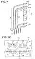
- FIG. 7is a perspective view of a set of signal terminals 261, 281 that are used in a signal terminal insert wafer 26 of the connectors of the present invention.
- FIG. 7also shows the relative position of the aforementioned retention clip 29.
- the signal terminal set 261 and 281is comprised of a top or outside conductor 261 A and a lower or inside conductor 261 B.
- conductive terminals 261 A, 261 Bcan be configured to be a differential signal pair.
- terminal 261Ais one terminal of one differential signal pair
- terminal 261 Bis one terminal of a second and distinct differential signal pair.
- These terminalshave corresponding differential signal terminals 54 which cooperatively define the differential signal terminal pair.
- the terminals 261A and 261 Beach have a first, or contact, portion 30 which are mirror images of each other. Together, they form a contact beam pair that will slide over the edge of a plug connector mating blade (typically a circuit card) when it is inserted into one of the receptacles 17 and 19.
- a plug connector mating bladetypically a circuit card
- terminal 261Ait includes a horizontal portion 34 that extends forward from a first point 32 away from an edge of the insulative wafer half into which it is molded.
- the first point 32is actually just beyond the front edge 49 of the first wafer half into which the terminals 261 and 281 are installed.
- the terminal 261 A horizontal portion 34extends "inwardly” to a second point 36 where the terminal 261 A turns downwardly toward the bottom edge 47 of the signal insert wafer 26.
- the vertical portion 38extends downwardly to a third point 40 whereat the terminal is formed into an "offset" 42 that travels inwardly as shown (toward the viewer in FIG. 7 ) in order to ensure that the tail portions are aligned along a line of action at the bottom of the signal terminal insert wafer.
- the compliant pin tails 44extend from the bottom of the offset 42 and can be inserted into a circuit board through hole.
- FIG. 7Adepicts a ground terminal for use in the aforementioned ground insert wafers.
- the ground terminalincludes compliant tail pins 45 that are electrically and mechanically connected together as a single unit.
- the ground terminal set shown in FIG. 7Aextend from the tail pins 45 to where it would exit receptacle slots 17 and 19.
- the ground terminal shown in FIG. 7Aprovides an isolating ground plane between signal wafer inserts installed into the connector 10.
- FIG.8is a perspective view of the two halves that make up a signal insert wafers and in particular, a perspective view of two sets of signal terminals 261, 281 with the insulative body portions of the insert wafer molded over the terminals (shown in FIG. 7 ).
- the signal insert wafer 26is comprised of a left half 50 and a right half 52.
- the terminals 26 and 28have portions that extend beyond the front edge 49 of the wafer half to form the aforementioned clip and extend parallel to the bottom edge 47 and the top edge 51 toward the rear edge 53. Near the rear edge 53, the terminals turn downwardly toward the rear edge 47 and exit as the aforementioned compliant tails 44.
- the signal terminal tail portions of the two wafer halvesextend toward each other near the tail portions so that they may arrive at the in-line tail arrangement that is present at the bottom of the signal insert wafer.
- a series of notches 55 and teeth 57(or “valleys” and “peaks") that run most of the length of the bottom edge 47.
- a notch 55is formed immediately in front of the rear edge 53 of the left half of the signal insert wafer.
- a tooth 59is formed that is immediately in front of the rear edge 53 of the right half 52 such that the tooth 59 on the right-hand half 52 of the signal insert wafer 26 will engage the notch 55 that is immediately in front of the rear edge 53 of the left half 50.
- the signal insert wafer 24includes a left half 50 and a right half 52.
- the left half 52includes a relatively flat or planar insulative body 63 that is, of course, made of a non-conductive material.
- the right half 52is also comprised of a relatively flat or planar insulative body 65 that is sized and shaped to mate with the left body 63.
- Both the spacer body 63 and the right body 65have a "front" edge identified by reference numeral 49. Both bodies have a "bottom” edge 47 as well as a "top” edge 51.
- the rear edge 53is considered to be “opposed" to the front edge 49; the top edge 51 is considered to be opposite the bottom edge 47.
- FIG. 9Ais the same view as FIG. 8 , but illustrates the two signal terminal wafer insert halves 50 and 52 assembled together to form a single signal terminal insert wafer 24.
- the compliant pin tails 44 that extend downwardly from the bottom edge 47are co-linear because they lie in the same plane (not shown).
- the side-by-side positions of differential terminals 62 and 54 at the front edge 49 of the signal insert wafer 24become front-to-back positions 62 and 54 when these same terminals exit the signal insert wafer 24 from its bottom edge 47.
- the rearrangement of the differential terminalsis enabled by different and opposing offsets 42 in the left and right halves 50 and 52 of a signal insert wafer.
- the first signal terminals 261 A and 26 1 Bare fixed into the planar left-side spacer body 63 such that they each have a horizontal portion 34 that extends to a vertical portion 38.
- Both terminals 261A and 261Bare substantially co-planar, meaning that they lie in a first plane and are adjacent to each other.
- the vertical portions 38 of each terminal 261A and 261 Brun to an offset section or segment 42, which in the left side body 63 extends the terminals 261A and 261B upwardly from the plane in which they both lie, to a second plane that is parallel to but elevated from first plane in which the terminals 261 A and 261 B both lie.
- Both offsets 42continue downwardly past the bottom edge 47 of the left side body 63 at where they become the compliant pin tail portions 44 of the terminal set.
- offsets in the right halfwhich are not shown, that extend the terminals in the third plane to the aforementioned second plane such that the pin tails 44 that extend from the bottom edge 47 of the right half 52 will be co-planar with the pin tails 44 that extend from the left half 50 when the two halves are assembled together.
- the halves 50, 52 of the signal insert wafermay be assembled together with posts and holes as shown in FIG. 8 and they may be further connected such as a heat or ultrasonic welding.
- the signal terminals in the right side body 65have a second offset that extends the terminals away from the third plane in a second direction to the aforementioned second plane from which they extend downwardly past the bottom edge of the wafer insert body.
- the extensions of the left side terminals and right side terminalsare laterally displaced from each other, i.e., they are spaced apart from each other as shown in FIG. 9A .
- FIG. 9Bis the same view as FIG. 9A but taken along the bottom of the signal insert wafer 26 to illustrate the edge-to-edge alignment of the signal terminal tails 44 along the bottom edge 47 of the signal insert wafer 26 halves 50 and 52.
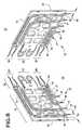
- FIG. 10Ais a perspective view of the signal insert wafer 26 of FIG. 9 flanked by two ground insert wafers 24. As stated above, the ground insert wafers 24 provide isolation for the signal insert wafers 26.
- FIG. 10Bis a perspective of the three insert wafers 24 and 26 assembled together to form a single signal transmission unit 70. As can be seen in the figure, the compliant pin tails 45 of the ground insert wafer are co-planar and therefore lie alone the same line. Similarly for the compliant pin tails 44 of the signal insert wafer 26, they are co-planar when they exit the bottom edge and lie along the same line.
- FIG. 10Cis a bottom plan view of the single signal transmission unit 70.
- each signal terminal 44forms the apex of a triangle, the other corners of which are two ground terminals 45.
- Signal "leakage” from any one of the signal pin tails 44is minimized because of the relatively close proximity of ground terminals 45 to which signals from the signal pin tails are capacitively shunted.
- each differential signal pair " DSP"lies within a geometric figure that is formed by interconnecting the four ground terminals 45 by imaginary lines. This is illustrated in the inset to the right of FIG. 10C .
- the geometric figure in the embodiments shownapproximate a square or a rectangle and other figures may be used in their place, preferably four-sided figures.
- FIG. 10CThe geometric figure in the embodiments shown approximate a square or a rectangle and other figures may be used in their place, preferably four-sided figures.
- the tail portionsare fully transitioned from the side-by-side arrangement in the contact portions thereof, where broadside capacitive coupling occurs, to and edge-to-edge arrangement in the tail portions where the terminals are connected to a circuit board.
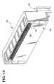
- FIGS. 14-19show an alternate embodiment of a connector 300 constructed in accordance with principles of the present invention, which utilizes a housing 302 with only one receptacle slot 304.
- the housing 302has a plurality of walls and the receptacle slot 304 is defined in the front wall 306.
- Posts 307 that receive mounting screwsare show sectioned in this embodiment which are used to mount the connector 300 to a circuit board 13.
- the rear of the connector 300includes a hollow cavity 309 that accommodates terminal inserts 310. Similar to the embodiments explained above, the cavity 309 has a series of slots 312, 313 of different heights, with the slot 312 really being a land as previously described. The difference in heights of the slots 312, 313 matches the difference in height of the signal insert wafers and ground insert wafers.
- the cavityalso includes a retention rib 314 which the terminal insert wafers engage with retention clips.
- FIG. 16illustrates the connector 300 with one of the signal insert wafers 320 partially removed from the cavity 309, and the ground insert wafer 322 left in place in the cavity.
- FIG. 17illustrates the signal insert wafer 320 as removed from the connector 300. It can be seen that it includes two pairs of terminals 325, 326 which are aligned with each other broadside, or widthwise, as shown in the other embodiments and with respect to the connector receptacle slot 304. These terminal pairs have contact portions 325A, 326A, body portions 325B, 326B and tail portions 325C, 326C. The tail portions 325C and 326C are aligned lengthwise, or edge-to-edge with respect to each other.
- the contact portions 325A, 3256Aare aligned horizontally along a line of action A-A shown in FIG. 17
- the tails portions 325C, 326Care aligned along a lengthwise line of action B-B as shown in FIG. 17 , which is offset from line of action A-A , and preferably at an angle of 90 degrees thereto, hence the reason why we refer to the tail portions being 90 degrees offset from the contact portions.
- the signal insert wafer 320is formed from two engaging halves 320A and 320B.
- FIG. 19illustrates one set of the terminals that make of the terminal pairs in FIG. 17 .
- FIG. 11is a top plan view of a circuit board layout used in conjunction with the connectors of FIG. 1 .
- each through hole for a signal pinis closely bounded by at least two ground leads or through holes that are intended to receive ground pins therein. That the closest pins to a signal lead are ground pins tends to shunt signals from a signal pin to ground potential thus reducing the likelihood that a signal on one set of differential pairs will be coupled to another differential signal pair.
- This circuit board arrangementminimizes cross talk between differential signal pairs in that at the circuit board level, there are four ground terminals extending into the circuit board that encompass each differential signal pair.
- ground terminals of the connectors of the inventionare commoned together near the circuit board level and this commoning bar also provide a short path from a differential signal terminal to the nearest reference ground terminal set.
- Each differential signal tail portion holeis at the apex of an imaginary triangle in which the other two apices are formed by intersecting lines drawn through the two closest ground terminal tail portion holes. This arrangement is shown to the left of FIG. 11 , where " S+ " represents a positive differential signal through hole of a signal pair and " S- " represents a negative differential signal through hole of that signal pair and " G " represents ground signal through holes of the circuit board.
- FIG. 12is an enlarged detail view of a portion of FIG. 11 , illustrating the use of an anti-pad style opening in a ground plane layer of the circuit board 110 of FIG. 11 .
- Thisis a top plane view and it illustrates signal through holes, or vias 113 and ground through holes, or vias 112.
- the signal viasare arranged in line with each other along an axis L1 .
- Two of the signal vias 113are closely spaced to each other to form a pair of differential signal vias 114 and so accommodate the tail portions of the signal terminal insert wafer.
- the remaining vias 112are connected to the ground plane 111 and these vias are also arranged in rows that flank the signal via pairs.
- An anti-pad 116may be included and this "anti-pad" refers to an area in which the conductive material that forms the ground plane 11 has been removed. Remaining in these open areas are annular conductive rings 115.
- the openings shown in FIG. 12are five-sided and take a polygonal shape, and are oriented as illustrated so that one line of ground vias (that shown above the top row of signal vias in FIG. 12 ) is proximate to the sharp corners (90 degrees) of the openings 116, while the other and opposite line of ground vias, those shown below the top row of signal vias in FIG. 12 are spaced further away from the angled edges of the openings 116.
- ground viaswould be located proximate the corners of the anti-pad. These ground vias may be considered as defining an imaginary four-sided figure, the perimeter of which encloses the anti-pad structures.
- FIG. 13is an enlarged detail view of a portion of the circuit board of FIG. 11 , illustrating another ground plane layer and signal trace route out construction suitable for use with connectors of the present invention.
- the pentagon-like opening 116has been split into two openings, 116a, each of which encompasses a single signal via 113 of a pair 114 of differential signal vias 113.
- the two openings 116aare spilt by a thin extension strip 120 of the ground plane that cuts across, and preferably bisects, the opening 116 into two substantially equal openings 116a.
- the circuit traces that exit the signal vias 113are shown in phantom in FIG. 13 . They include flag portions or the like 121 that extend toward each other from the vias 113. Those flag portions are joined to first strip portions 122 that run in a circuit board layer underneath (or above) the ground plane layer 111. These first portions, as shown, extend beneath the center bisecting trip 120 and they are preferably aligned with the strip 120 so that the outer edges of the first portions 122 align themselves with the outer edges of the strip 120 (or the inner edges of the two openings 116a on opposite sides of the strip 120. Second conductive portions 123 are shown joined to the first portions 122 and are shown extending at an angle thereto.
- Third and fourth portions 124, 125are also joined to the second and third portions, respectively, at angles so that the circuit traces tend to follow the outer configuration of the opening 116a on the left of the strip 120 in FIG. 13 . This is to give these circuit traces a ground plane or strip of particular configuration to couple with.
Landscapes
- Engineering & Computer Science (AREA)
- Microelectronics & Electronic Packaging (AREA)
- Physics & Mathematics (AREA)
- Electromagnetism (AREA)
- Details Of Connecting Devices For Male And Female Coupling (AREA)
- Connector Housings Or Holding Contact Members (AREA)
- Coupling Device And Connection With Printed Circuit (AREA)
Description
- This invention relates generally to high speed connectors that are used as vertically stacked receptacle connectors, and more particularly, to connectors utilizing insert wafers that incorporate differential signal terminals which are positioned alongside each other where they appear in the connector receptacle portions and which are turned at their tail portions for joining to a printed circuit board.
- Electrical connectors are well known to those of ordinary skill in the electronic arts as generally reliable devices by which electrical signal paths can be extended into and obtained from a printed circuit board. Over the last several years, however, electronic devices and systems have gotten both smaller and faster, making reliable connectors more difficult to design, manufacture and install onto printed circuit boards.
- In a connector used in high-speed applications, crosstalk that is likely to occur between closely spaced, high-speed signal paths can be reduced by using differential-voltage signals. A differential signal pair is a pair of terminals or other conductors that together carry a signal but neither of the two conductors is at ground or reference potential. Rather, the voltage on one conductor of a differential pair is, at any given instant, the same magnitude, but opposite polarity as the voltage on the other conductor. A differential pair therefore is analogous to a transmission line, the conductors of which are capacitively and inductively coupled to each other. Crosstalk between two or more differential signal pairs as well as interference of one differential pair on another can be significantly reduced if a good ground plane (or other fixed-voltage reference plane) is provided between the conductors of one differential pair and the conductors of another differential pair as a sort of shield between them.
- Each differential signal pair requires at least two capacitively coupled conductors, and it is important for a connector that links a differential signal pair between devices or circuit boards to maintain capacitive coupling. When a connector is used to provide an edge connection for a circuit board or is used as a plug connector, arranging differential signal pairs in a connector so that they are alongside each other and next to each other on the same side of a circuit board can cause the connector width to increase, but when the connector is installed onto a circuit board, connector width should be minimized. This problem is solved by the features of the characterizing portion of
claim 1. EP1311038 discloses connector, comprising:- an insulative housing, the housing having a mating face for engaging with an opposing connector, and a mounting face for mounting the connector to a circuit board; and
- a plurality of conductive terminals supported in the housing, the terminals being arranged into sets of one pair of differential signal terminals and a pair of ground terminals, each of the terminals having contact portions that extend along the connector mating face and tail portions that extend along the connector mounting face and body portion that interconnect the contact and terminal portions together, the pair of differential signal terminals being arranged at their contact portions side-by-side in order to effect broadside capacitive coupling between said contact portions of said pair of differential signal terminals and the tail portions of said pair of differential signal terminals are configured to provide an edge-to-edge coupling between said pair of differential signal terminals.
WO-A-0157964 claim 1.- It is therefore a general object of the present invention to provide a circuit board connector which provides one or more receptacle connector, each of which will accept the edge connector of a circuit board or like device.
- Another object of the present invention is to provide a stacked receptacle connector, each receptacle of which will accommodate differential signal pairs. Yet another object of the present invention is to provide a stacked receptacle connector that enables differential signal pairs to be installed into a connector body using individual inserts in the form of wafers, each of which is relatively easy to manufacture and each of which also allows ground planes to be provided between each wafer insert in an encompassing connector housing.
- Another object of the present invention is to provide a connector for use in high speed applications, the connector including an insulative housing with a hollow interior cavity, the cavity accommodating a plurality of terminal signal and ground terminal inserts in the form of thin wafers, each wafer supporting a plurality of conductive terminals, the terminals having contact portions, tail portions and body
- portions interconnecting the contact and tail portions together, the signal terminals being disposed so that most of the terminals are oriented with their wider sides arranged vertically for broadside capacitive coupling to adjacent corresponding terminals in adjacent wafers, and a small part of the signal terminal body and tail portions being bent and offset about 90 degrees so that the signal terminals are arranged in an edge-to-edge arrangement at the terminal tail portions.
- Still another object of the present invention is to provide a connector for use with high speed differential signal applications in which terminals are held in assemblies that preferably take the form of insulative wafers, two wafers with conductive signal terminal being assembled together to form a signal terminal wafer assembly and two wafers that contain conductive ground terminals being arranged on opposite sides of the signal terminal assembly to provide reference ground terminal arrangements that flank the signal terminal assembly, the signal terminals having contact portion that are arranged in side-by-side order and termination portions that are arranged in edge-to-edge order. A still further object of the present invention is to provide a unique circuit board layout for accommodating the tail portions of connectors of the structure described above, which circuit board layout facilities the high speed operation of connectors of the invention.
- Yet another object of the present invention is to provide a circuit board with a particular arrangement of traces that enhance the high speed transmission abilities of the connectors of the invention, the circuit board having a plurality of conductive traces extending to mounting through holes disposed in a circuit board, the through holes being arranged in a pattern such that a plurality of ground traces encompass a pair of differential signal traces, and in which the ground traces are arranged at the corners of a four-sided figure, with the differential signal through holes arranged in line within a perimeter defined by the ground through holes.
- These and other objects of the present invention are accomplished by way of the structure of the invention. A connector is provided with an insulative housing that has two or more receptacle portions, each of which is capable of accepting a card edge of other similar blade portion of an opposing electronic device, such as an electronic or opto-electronic module. The receptacle connectors of the invention include a plurality of pairs of differential signal terminals, and the terminals have a unique structure which permits them be broadside coupled in pairs along one extent of the connector, and subsequently edge coupled along a remaining extent of the connector.
- Multiple inserts are provided which carry terminal that are intended to be designated as carrying differential signals. In this regard, multiple differential signal terminal pairs are supported in an insulative wafer that may be inserted into the connector housing. The signal terminal insert is preferably formed from two interengaging halves, and the terminals of each differential signal pair are spaced apart from each other in a parallel fashion. This is carried on from the terminal contact portions rearwardly in the terminal body portions to a location near the tail portions of the terminals.
- The differential signal terminals conductors have their paths rotated in their supporting insert wafer so that they turn about 90 degrees near where the terminal body portions end and this turn extends into the terminal tail portions. Thus, the signal terminals are arranged in a line and are spaced apart along that line in an edge-to-edge arrangement. In this fashion, the terminals may engage in edge coupling along their tail portions and broadside coupling along their contact and body portions.
- The halves of the signal terminal wafer inserts have serrated-style bases on which are formed alternating projections and recesses, with the projections of the first of the two insert wafer halves being received within the recesses of the second of the two signal insert wafer halves and vice-versa. In this manner the terminal tails portions are easily arranged in a line in the edge-to-edge fashion stated above.
- Additional insert wafers are provided and are arranged in spaces provided between the signal terminal assemblies and these act as ground planes between adjoining signal terminal insert wafers to isolate signals carried through the signal wafers. The heights of the signal and ground insert wafers are different so as to polarize the insert wafers and the connector housing so that ground insert wafers cannot be inserted into a portion of the connector housing that is dedicated to receive a ground terminal insert wafer. Likewise, the connector housing is formed with different wafer-receiving slots, so that a ground wafer slot is capable of receiving only a ground terminal wafer and a signal terminal slot is capable of receiving only a signal terminal wafer assembly.
- These and other objects, features and advantages of the present invention will be clearly understood through a consideration of the following detailed description
- In the course of this description, references will be made to the drawings, in which:
FIG. 1 is a perspective view of a connector that is constructed in accordance with the principles of the present invention;FIG. 2 is a perspective view of the connector ofFIG. 1 , taken from the rear thereof, with all but three insert wafers removed from the interior fo the connector for clarity;FIG. 3 is a sectional view of the connector ofFIG. 1 , taken from the rear and illustrating four ground insert wafers in place within the interior of the connector housing;FIG. 4 is the same sectional view asFIG. 3 , but illustrating three signal insert wafers in place within the interior of the connector housing;FIG. 5 is the same view asFIG. 4 , but illustrating one of the three signal inserts partially in place in the connector housing between two adjoining ground insert wafers and illustrating two signal insert wafers aligned with their respective openings in the connector housing;FIG. 6 is the same view asFIG. 3 , with the ground insert wafers removed to illustrate the interior of the connector housing;FIG. 7 is a perspective view of a set of terminals used in a signal insert wafer used in the connector ofFIG. 1 ;FIG. 7A is a perspective view of a set of terminals used in a ground insert wafer used in the connector ofFIG. 1 ;FIG. 8 is a perspective view of two sets of signal terminals with insulative body portions molded thereover, and facing in opposition to each other for subsequent assembly;FIG. 9A is the same view asFIG. 8 , but illustrating the two signal insert wafer halves assembled together to form a single signal insert wafer;FIG. 9B is the same view asFIG. 9A but taken along the bottom of the signal insert wafer to illustrate the alignment of the signal terminal tails along the bottom edges of the signal insert wafer;FIG. 10A is a perspective view of the signal insert wafer ofFIG. 9 flanked by two ground insert wafers;FIG. 10B is a perspective of all of the three (ground-signal-ground) insert wafers ofFIG. 10B assembled together to form a single signal transmission unit;FIG. 10C is a bottom plan view of the single signal insert wafer ofFIG. 10A illustrating the orientation and layout of the tail portions of the terminals of the signal and ground insert wafers;FIG. 11 is a top plan view of a circuit board layout used in conjunction with the connectors ofFIG. 1 ;FIG. 12 is an enlarged detail view of a portion ofFIG. 11 , illustrating the use of an anti-pad style opening in a ground plane layer of the circuit board ofFIG. 11 ;FIG. 13 is an enlarged detail view of a portion of the circuit board ofFIG. 11 , illustrating another ground plane layer and signal trace route out construction suitable for use with connectors of the present invention.FIG. 14 is a perspective view of an alternate embodiment of a connector constructed in accordance with the principles of the present invention , but having only a single card-receiving, or mating slot for mating with an opposing connector;FIG. 1 is a view of the connector ofFIG. 14 , taken from the rear;FIG. 16 is the same view asFIG. 15 , but with the connector and its terminal assemblies removed from the circuit board and with a signal terminal assembly shown partially removed from the connector for clarity;FIG. 17 is a perspective view of a signal terminal assembly used in the connector ofFIG. 14 ;FIG. 18 is the same view asFIG. 17 , but with the signal terminal assembly halves removed for clarity; and,FIG. 19 is a view of the terminal used in one of the signal terminal assembly halves ofFIG. 17 .- Referring now to
FIG. 1 , there is shown a perspective view of aconnector 10 that is constructed in accordance with the principles of the present invention. Theconnector 10 has atop surface 12, afront face 14, abottom surface 16 and left and right side surfaces, or faces, 18 and 20. As can be seen inFIG. 1 , theconnector 10 front face has tworeceptacle portions circuit board 13 to which thebase connector 10 is attached. Theconnector 10 of the present invention is a compressible attachment-style connector, meaning that it is attached to a circuit board by means of through hole pins, that as explained below, are shown in the embodiment depicted as compliant pins. - The connector also has a
rear face 20, which is shown more clearly inFIG. 2 , which is a perspective view of theconnector 10 ofFIG. 1 , but taken from the rear thereof and looking into at therear face 22 of the connector and into the hollowinterior cavity 25 of theconnector 10. At the left-hand side of therear face 22 of the connector housing, there are shown three separate insert wafers, two of which are identified byreference numeral 24, the other of which is identified byreference numeral 26. As described more fully below, the insert wafers are of two types: aground insert wafer 24 and asignal insert wafer 26 and the type is based upon the type of signals that are carried by the conductive terminals in each of the insert wafers. A signal insert wafer is intended to carry multiple signal signals, and particularly, pairs of differential signals. A ground insert wafer is intended to be connected to one or more ground planes on the circuit board and its terminals will carry ground signals as opposed to differential signals. - In the preferred embodiment of the
connector 10 illustrated, eachsignal insert wafer 26 is installed between twoground insert wafers 24 as shown inFIG. 2 . In this manner, the differential signal terminals of each pair may be maintained and directed within theinsert wafer 26, but they are flanked by ground terminals that provide close ground paths that somewhat surround the signal pairs. This structure assists in providing maximum shielding of thesignal insert wafer 26 and results in a reduction of EMI and signal cross talk and skew with or by other signal insert wafers that are present in theconnector 10. FIG. 3 is a sectional view of theconnector 10 ofFIG. 1 , taken from the rear 22 of theFIG. 3 is a sectional view of theconnector 10 ofFIG. 1 , taken from the rear 22 of theconnector 10 and illustrating fourground insert wafers 24 installed within the interior of the connector housing and three signal-receiving slots interposed between the ground insert wafers.FIG. 4 , illustrates the same view with thesignal insert wafers 26 inserted in place. As can be seen inFIG. 3 , each of theground insert wafers 24 have compliant signal tail pins 45 that project from thebottom edge 47 of eachground insert wafer 24 and are co-linear along a longitudinal axis of the signal insert wafer.FIG. 4 is the same view of therear face 22 ofconnector 10 as shown inFIG. 3 , but with threesignal insert wafers 26 installed into theconnector 10. Like theground insert wafers 24, thesignal insert wafers 26 also havecompliant pin tails 44 that project from thebottom edge 47 of eachsignal insert wafer 26 along the same line and are also co-linear.FIG. 5 is the same view asFIG. 4 , but it illustrates one of the threesignal insert wafers 26 partially in place in theconnector 10 between two adjoining (or flanking)ground insert wafers 24. Thesignal insert wafers 26 and theground insert wafers 24 have different heights so that they can be easily matched into their corresponding proper positions within theinterior cavity 25 of theconnector housing 10. By making thesignal insert wafers 26 of one height and the ground insert wafers 24 a different height, and making the signal insert wafer slot and ground insert wafer slots of theconnector 10 to be of similar corresponding heights, the possibility of incorrectly installing a ground insert wafer 24 (taller) into a signal insert wafer slot or of installing a signal insert wafer into a position that is designated for a ground insert wafer is eliminated. This speeds up assembly and repair of the connectors of the invention. The ground insert wafers are fit into slots 100 (FIG. 3 ) that are formed along at least one surface of theinterior cavity 25 of theconnector housing 10, while the signal insert wafers fit against the interveningland portions 101 that are arranged between theslots 100. The heights of the signal and ground insert wafers may reversed, if desired, that is the signal insert wafers can be made taller than the ground insert wafers and the housing modified to accommodate this arrangement.FIG. 6 is the same view asFIG. 3 , with theground insert wafers 24 removed for clarity in order to illustrate theinterior cavity 25 of theconnector 10 housing and clearly showing a insert wafer retention andalignment rib 27 that is formed as part of theconnector 10 housing and which runs horizontally between thestacked receptacles 17 and 19 (FIG. 1 ) into which a circuit board, device or connector can be inserted. Thisrib 27 is sized and structured so that theretention clip 29 that is formed as part of eachinsert wafer alignment rib 27 and holds theinsert wafers connector 10 as plug connectors (not shown) are inserted into and removed from theconnector housing 10. Additionally, theconnector housing 10, may, on opposite sides of thealignment rib 27, include a plurality ofsecondary slots 102, each of which receives edges of the retention clips 29 of thesignal insert wafer 26 and theground insert wafers 24. The terminals, as explained below, may includeretention barbs 104 that engage the inner surfaces of terminal-receivingcavities 105 of theconnector housing 10.- As set forth above, the use of differential signals on a circuit board or other device requires two conductors to carry one differential signal with each conductor carrying an equal but opposite polarity signal as its mate. When the
stacked receptacles receptacle circuit board 13 to which theconnector 10 is attached. Therefore, in order to accommodate the attachment of many differential signal pairs from thetop receptacle 19 and those required of thebottom receptacle 17 in the width of theconnector 10, the differential signal pairs provided to eachreceptacle connector 10 to thecircuit board 13 are aligned "front-to-back" or "edge-to-edge" as shown inFIG. 10C , where theconnector 10 meets acircuit board 13 instead of "side-to-side" where a circuit board would be inserted into one of thereceptacles FIG. 7 is a perspective view of a set ofsignal terminals terminal insert wafer 26 of the connectors of the present invention.FIG. 7 also shows the relative position of theaforementioned retention clip 29. Because the sets ofsignal terminals signal terminals 261 is described hereinafter. The signal terminal set 261 and 281 is comprised of a top oroutside conductor 261 A and a lower or insideconductor 261 B. In one embodiment,conductive terminals FIG. 8 , terminal 261A is one terminal of one differential signal pair and terminal 261 B is one terminal of a second and distinct differential signal pair. These terminals have correspondingdifferential signal terminals 54 which cooperatively define the differential signal terminal pair.- Still referring to
FIG. 7 , it can be seen that theterminals portion 30 which are mirror images of each other. Together, they form a contact beam pair that will slide over the edge of a plug connector mating blade (typically a circuit card) when it is inserted into one of thereceptacles horizontal portion 34 that extends forward from afirst point 32 away from an edge of the insulative wafer half into which it is molded. As can be seen inFIG. 8 , thefirst point 32 is actually just beyond thefront edge 49 of the first wafer half into which theterminals horizontal portion 34 extends "inwardly" to asecond point 36 where the terminal 261 A turns downwardly toward thebottom edge 47 of thesignal insert wafer 26. Thevertical portion 38 extends downwardly to athird point 40 whereat the terminal is formed into an "offset" 42 that travels inwardly as shown (toward the viewer inFIG. 7 ) in order to ensure that the tail portions are aligned along a line of action at the bottom of the signal terminal insert wafer. Thecompliant pin tails 44 extend from the bottom of the offset 42 and can be inserted into a circuit board through hole. FIG. 7A depicts a ground terminal for use in the aforementioned ground insert wafers. As can be seen, the ground terminal includes compliant tail pins 45 that are electrically and mechanically connected together as a single unit. The ground terminal set shown inFIG. 7A extend from the tail pins 45 to where it would exitreceptacle slots FIG. 7A provides an isolating ground plane between signal wafer inserts installed into theconnector 10.FIG.8 is a perspective view of the two halves that make up a signal insert wafers and in particular, a perspective view of two sets ofsignal terminals FIG. 7 ). As shown in the figure, thesignal insert wafer 26 is comprised of aleft half 50 and aright half 52. With respect now to just theleft half 50, it can be seen that theterminals 26 and 28 have portions that extend beyond thefront edge 49 of the wafer half to form the aforementioned clip and extend parallel to thebottom edge 47 and thetop edge 51 toward therear edge 53. Near therear edge 53, the terminals turn downwardly toward therear edge 47 and exit as the aforementionedcompliant tails 44. The signal terminal tail portions of the two wafer halves extend toward each other near the tail portions so that they may arrive at the in-line tail arrangement that is present at the bottom of the signal insert wafer.- Just above the
bottom edge 47 of theleft half 50 of thesignal insert wafer 26 there are a series ofnotches 55 and teeth 57 (or "valleys" and "peaks") that run most of the length of thebottom edge 47. In particular, however, anotch 55 is formed immediately in front of therear edge 53 of the left half of the signal insert wafer. On theright half 52 of the signal insert wafer's 26bottom edge 47, atooth 59 is formed that is immediately in front of therear edge 53 of theright half 52 such that thetooth 59 on the right-hand half 52 of thesignal insert wafer 26 will engage thenotch 55 that is immediately in front of therear edge 53 of theleft half 50. When the left andright halves notches 55 andteeth 57 of theleft half 52 engage theteeth 59 andnotches 61 of theright half 52 in a sort of "sawtooth" engagement of each half to the other. This sawtooth, or serrated, arrangement permits the tail portions of the signal terminals to come out of plane and be aligned linearly along the bottom edge of the signal terminal insert wafer. - It can be seen in
FIG. 8 that thesignal insert wafer 24 includes aleft half 50 and aright half 52. Theleft half 52 includes a relatively flat or planarinsulative body 63 that is, of course, made of a non-conductive material. Theright half 52 is also comprised of a relatively flat or planarinsulative body 65 that is sized and shaped to mate with theleft body 63. Both thespacer body 63 and theright body 65 have a "front" edge identified byreference numeral 49. Both bodies have a "bottom"edge 47 as well as a "top"edge 51. Therear edge 53 is considered to be "opposed" to thefront edge 49; thetop edge 51 is considered to be opposite thebottom edge 47. - The terminals depicted in
FIG. 7 run through each of theleft half 50 and theright half 52 and are identical except for one small but very important aspect.FIG. 9A is the same view asFIG. 8 , but illustrates the two signal terminal wafer insert halves 50 and 52 assembled together to form a single signalterminal insert wafer 24. As can be seen inFIG. 9A , thecompliant pin tails 44 that extend downwardly from thebottom edge 47 are co-linear because they lie in the same plane (not shown). Stated alternatively, the side-by-side positions ofdifferential terminals front edge 49 of thesignal insert wafer 24 become front-to-back positions signal insert wafer 24 from itsbottom edge 47. The rearrangement of the differential terminals is enabled by different and opposingoffsets 42 in the left andright halves - In
FIG. 7 andFIG. 8 , thefirst signal terminals side spacer body 63 such that they each have ahorizontal portion 34 that extends to avertical portion 38. Bothterminals vertical portions 38 of each terminal 261A and 261 B run to an offset section orsegment 42, which in theleft side body 63 extends theterminals terminals bottom edge 47 of theleft side body 63 at where they become the compliantpin tail portions 44 of the terminal set. - In the
right half 52 of thesignal insert wafer 26, there are terminals identical toterminals signal wafer half 52, they lie in a third plane, which is parallel to and displaced or offset from the first plane in whichterminals pin tails 44 that extend from thebottom edge 47 of theright half 52 will be co-planar with thepin tails 44 that extend from theleft half 50 when the two halves are assembled together. Thehalves FIG. 8 and they may be further connected such as a heat or ultrasonic welding. - In claim parlance, the signal terminals in the
right side body 65 have a second offset that extends the terminals away from the third plane in a second direction to the aforementioned second plane from which they extend downwardly past the bottom edge of the wafer insert body. The extensions of the left side terminals and right side terminals are laterally displaced from each other, i.e., they are spaced apart from each other as shown inFIG. 9A . FIG. 9B is the same view asFIG. 9A but taken along the bottom of thesignal insert wafer 26 to illustrate the edge-to-edge alignment of thesignal terminal tails 44 along thebottom edge 47 of thesignal insert wafer 26halves FIG. 10A is a perspective view of thesignal insert wafer 26 ofFIG. 9 flanked by twoground insert wafers 24. As stated above, theground insert wafers 24 provide isolation for thesignal insert wafers 26.FIG. 10B is a perspective of the threeinsert wafers signal transmission unit 70. As can be seen in the figure, thecompliant pin tails 45 of the ground insert wafer are co-planar and therefore lie alone the same line. Similarly for thecompliant pin tails 44 of thesignal insert wafer 26, they are co-planar when they exit the bottom edge and lie along the same line.FIG. 10C is a bottom plan view of the singlesignal transmission unit 70. As can be seen in this figure, eachsignal terminal 44 forms the apex of a triangle, the other corners of which are twoground terminals 45. Signal "leakage" from any one of thesignal pin tails 44 is minimized because of the relatively close proximity ofground terminals 45 to which signals from the signal pin tails are capacitively shunted. Additionally, each differential signal pair "DSP" lies within a geometric figure that is formed by interconnecting the fourground terminals 45 by imaginary lines. This is illustrated in the inset to the right ofFIG. 10C . The geometric figure in the embodiments shown approximate a square or a rectangle and other figures may be used in their place, preferably four-sided figures.FIG. 10C also explains the order of the terminals relative to the differential signal contact portions shown inFIG. 9A . As shown, the tail portions are fully transitioned from the side-by-side arrangement in the contact portions thereof, where broadside capacitive coupling occurs, to and edge-to-edge arrangement in the tail portions where the terminals are connected to a circuit board.FIGS. 14-19 show an alternate embodiment of aconnector 300 constructed in accordance with principles of the present invention, which utilizes ahousing 302 with only onereceptacle slot 304. Thehousing 302 has a plurality of walls and thereceptacle slot 304 is defined in thefront wall 306.Posts 307 that receive mounting screws are show sectioned in this embodiment which are used to mount theconnector 300 to acircuit board 13. As shown inFIG. 15 , the rear of theconnector 300 includes ahollow cavity 309 that accommodates terminal inserts 310. Similar to the embodiments explained above, thecavity 309 has a series ofslots slot 312 really being a land as previously described. The difference in heights of theslots retention rib 314 which the terminal insert wafers engage with retention clips.FIG. 16 illustrates theconnector 300 with one of thesignal insert wafers 320 partially removed from thecavity 309, and theground insert wafer 322 left in place in the cavity.FIG. 17 illustrates thesignal insert wafer 320 as removed from theconnector 300. It can be seen that it includes two pairs ofterminals connector receptacle slot 304. These terminal pairs havecontact portions body portions tail portions tail portions contact portions 325A, 3256A are aligned horizontally along a line of actionA-A shown inFIG. 17 , thetails portions FIG. 17 , which is offset from line of actionA-A, and preferably at an angle of 90 degrees thereto, hence the reason why we refer to the tail portions being 90 degrees offset from the contact portions.- As shown in
FIG 18 , thesignal insert wafer 320 is formed from twoengaging halves FIG. 19 illustrates one set of the terminals that make of the terminal pairs inFIG. 17 . FIG. 11 is a top plan view of a circuit board layout used in conjunction with the connectors ofFIG. 1 . As can be seen inFIG. 11 , each through hole for a signal pin is closely bounded by at least two ground leads or through holes that are intended to receive ground pins therein. That the closest pins to a signal lead are ground pins tends to shunt signals from a signal pin to ground potential thus reducing the likelihood that a signal on one set of differential pairs will be coupled to another differential signal pair. This circuit board arrangement minimizes cross talk between differential signal pairs in that at the circuit board level, there are four ground terminals extending into the circuit board that encompass each differential signal pair. Additionally, the ground terminals of the connectors of the invention are commoned together near the circuit board level and this commoning bar also provide a short path from a differential signal terminal to the nearest reference ground terminal set. Each differential signal tail portion hole is at the apex of an imaginary triangle in which the other two apices are formed by intersecting lines drawn through the two closest ground terminal tail portion holes. This arrangement is shown to the left ofFIG. 11 , where "S+" represents a positive differential signal through hole of a signal pair and "S-" represents a negative differential signal through hole of that signal pair and "G" represents ground signal through holes of the circuit board.FIG. 12 is an enlarged detail view of a portion ofFIG. 11 , illustrating the use of an anti-pad style opening in a ground plane layer of thecircuit board 110 ofFIG. 11 . This is a top plane view and it illustrates signal through holes, orvias 113 and ground through holes, orvias 112. The signal vias are arranged in line with each other along an axisL1. Two of thesignal vias 113 are closely spaced to each other to form a pair ofdifferential signal vias 114 and so accommodate the tail portions of the signal terminal insert wafer. The remainingvias 112 are connected to theground plane 111 and these vias are also arranged in rows that flank the signal via pairs. An anti-pad 116, may be included and this "anti-pad" refers to an area in which the conductive material that forms the ground plane 11 has been removed. Remaining in these open areas are annular conductive rings 115. The openings shown inFIG. 12 are five-sided and take a polygonal shape, and are oriented as illustrated so that one line of ground vias (that shown above the top row of signal vias inFIG. 12 ) is proximate to the sharp corners (90 degrees) of theopenings 116, while the other and opposite line of ground vias, those shown below the top row of signal vias inFIG. 12 are spaced further away from the angled edges of theopenings 116. If the anti-pad structure of the circuit board were square, rather than a pentagon, the ground vias would be located proximate the corners of the anti-pad. These ground vias may be considered as defining an imaginary four-sided figure, the perimeter of which encloses the anti-pad structures.FIG. 13 is an enlarged detail view of a portion of the circuit board ofFIG. 11 , illustrating another ground plane layer and signal trace route out construction suitable for use with connectors of the present invention. In this arrangement, the pentagon-like opening 116 has been split into two openings, 116a, each of which encompasses a single signal via 113 of apair 114 ofdifferential signal vias 113. The twoopenings 116a are spilt by athin extension strip 120 of the ground plane that cuts across, and preferably bisects, theopening 116 into two substantiallyequal openings 116a.- The circuit traces that exit the
signal vias 113 are shown in phantom inFIG. 13 . They include flag portions or the like 121 that extend toward each other from thevias 113. Those flag portions are joined tofirst strip portions 122 that run in a circuit board layer underneath (or above) theground plane layer 111. These first portions, as shown, extend beneath thecenter bisecting trip 120 and they are preferably aligned with thestrip 120 so that the outer edges of thefirst portions 122 align themselves with the outer edges of the strip 120 (or the inner edges of the twoopenings 116a on opposite sides of thestrip 120. Secondconductive portions 123 are shown joined to thefirst portions 122 and are shown extending at an angle thereto. Third andfourth portions opening 116a on the left of thestrip 120 inFIG. 13 . This is to give these circuit traces a ground plane or strip of particular configuration to couple with. - While the preferred embodiments of the invention have been shown and described, it will be appreciated by those skilled in the art that changes and modifications may be made to these embodiments without departing from the scope of the invention which is defined by the appended claims.
Claims (8)
- A connector, comprising:an insulative housing, the housing having a mating (19) face for engaging with an opposing connector, and a mounting face (16) for mounting the connector to a circuit board (13); and,a plurality of conductive terminals supported in the housing, the terminals being arranged into sets of one pair of differential signal terminals and a pair of ground terminals, wherein each of the terminals has contact portions (261,54) that extend along the connector mating face and tail portions (44) that extend along the connector mounting face and body portion (38) that interconnect the contact and terminal portions together, and the tail portions (45) are configured to provide an edge-to-edge coupling between differential pairs, wherein each one of the terminals that make up the pair of differential signal terminals (261,54) is positioned in a signal insert wafer (26) in adjacent first and second insulative wafer halves (50,52) respectively, and each of the ground terminals that forms the pair of ground terminals is positioned in a separate ground insert wafer (24) for supporting the ground terminal, the ground and signal insert wafers (24,26) providing a ground-signal-signal-ground pattern of terminals,characterized in that the pair of differential signal terminals is arranged at their contact portions (261,54) side-by-side in order to effect broadside capacitive coupling between said contact portions of said pair of differential signal terminals.
- The connector of claim 1,characterized in that the pair (261,54) of differential signal terminals is a first pair of differential signal terminals, the connector further comprising a second pair of differential signal terminals (261,54), the first pair of differential signal terminals (261,54) positioned in the adjacent first and second signal wafer half (50,52) and the second pair of differential signal terminals (261,54) positioned in an adjacent third and fourth signal wafer half (50,52), the third and fourth signal wafer half (50,52) separated from the first and second signal wafer (26) by one of the ground wafers (24), the connector providing a repeating ground-signal-signal pattern.
- The connector of claim 1 or claim 2,characterized in that said terminal tail portions (44,45) include compliant pin portions.
- The connector of any preceding claim,characterized in that each of said first and second signal wafer halves (50,52) includes a plurality of teeth and notches (57,55,59,61) in alternating fashion along said connector mounting face, the teeth and notches being further arranged to interfit with each other such that the teeth (57) of said first wafer half (50) are received within the notches (61) of said second wafer half (52), and the teeth (59) of said second wafer half (52) are received within the notches (55) of said first wafer half (50).
- The connector of claim 4,characterized in that said tail portions (44) of said differential signal terminal pair are held within said teeth (57,59), one tail portion of said differential signal terminal pair being held within a tooth (57) of said first signal wafer half (50) and the other tail portion of said differential signal terminal pair being held within a tooth (59) of said second signal wafer half (52).
- The connector of any preceding claim,characterized in that each of the ground wafers (24) has two tail portions (45) adjacent each other so as to define four points of a geometric figure when imaginary lines are drawn interconnecting said ground terminal tail portions, said tail portions (44) of said differential signal terminal pair being disposed within a perimeter of said geometric figure.
- The connector of claim 6,characterized in that said geometric figure is a rectangular, four-sided figure.
- The connector of any preceding claim,characterized in that said first and second signal wafer halves (50,52) include channels formed therein that expose surfaces of said signal terminals (261,54) to air, thereby creating an air pocket between said signal terminals that form the differential pair.
Applications Claiming Priority (2)
| Application Number | Priority Date | Filing Date | Title |
|---|---|---|---|
| US65505105P | 2005-02-22 | 2005-02-22 | |
| PCT/US2006/006110WO2006091595A1 (en) | 2005-02-22 | 2006-02-22 | Differential signal connector with wafer-style construction |
Publications (2)
| Publication Number | Publication Date |
|---|---|
| EP1851833A1 EP1851833A1 (en) | 2007-11-07 |
| EP1851833B1true EP1851833B1 (en) | 2012-09-12 |
Family
ID=36406590
Family Applications (1)
| Application Number | Title | Priority Date | Filing Date |
|---|---|---|---|
| EP06735673ANot-in-forceEP1851833B1 (en) | 2005-02-22 | 2006-02-22 | Differential signal connector with wafer-style construction |
Country Status (5)
| Country | Link |
|---|---|
| US (4) | US7422483B2 (en) |
| EP (1) | EP1851833B1 (en) |
| JP (2) | JP4663741B2 (en) |
| CN (1) | CN101164204B (en) |
| WO (1) | WO2006091595A1 (en) |
Families Citing this family (115)
| Publication number | Priority date | Publication date | Assignee | Title |
|---|---|---|---|---|
| WO2005114274A1 (en)* | 2004-05-14 | 2005-12-01 | Molex Incorporated | Light pipe assembly for use with small form factor connector |
| CN101095381B (en)* | 2004-10-29 | 2010-06-16 | 莫莱克斯公司 | Printed circuit board for high speed electrical connector |
| JP4663741B2 (en)* | 2005-02-22 | 2011-04-06 | モレックス インコーポレイテド | Differential signal connector having wafer type structure |
| US7976345B2 (en)* | 2005-12-15 | 2011-07-12 | Tyco Electronics Corporation | Electrical contact assembly and method of manufacturing thereof |
| US7264509B1 (en)* | 2006-04-24 | 2007-09-04 | Tyco Electronics Corporation | Modular connector assembly utilizing a generic lead frame |
| US7450396B2 (en)* | 2006-09-28 | 2008-11-11 | Intel Corporation | Skew compensation by changing ground parasitic for traces |
| US20110203843A1 (en)* | 2006-10-13 | 2011-08-25 | Taras Kushta | Multilayer substrate |
| US7811100B2 (en) | 2007-07-13 | 2010-10-12 | Fci Americas Technology, Inc. | Electrical connector system having a continuous ground at the mating interface thereof |
| US8858490B2 (en) | 2007-07-18 | 2014-10-14 | Silk Road Medical, Inc. | Systems and methods for treating a carotid artery |
| EP2240980A2 (en) | 2008-01-17 | 2010-10-20 | Amphenol Corporation | Electrical connector assembly |
| US8764464B2 (en) | 2008-02-29 | 2014-07-01 | Fci Americas Technology Llc | Cross talk reduction for high speed electrical connectors |
| CN201204312Y (en)* | 2008-03-25 | 2009-03-04 | 富士康(昆山)电脑接插件有限公司 | electrical connector |
| CN201562835U (en)* | 2008-09-09 | 2010-08-25 | 莫列斯公司 | Shielding cover and connector component thereof |
| JP5405582B2 (en) | 2008-11-14 | 2014-02-05 | モレックス インコーポレイテド | Resonance change connector |
| MY155071A (en) | 2008-12-12 | 2015-08-28 | Molex Inc | Resonance modifying connector |
| US8021191B2 (en)* | 2008-12-12 | 2011-09-20 | Molex Incorporated | Connector with two-piece housing |
| US9011177B2 (en) | 2009-01-30 | 2015-04-21 | Molex Incorporated | High speed bypass cable assembly |
| CN102405564B (en)* | 2009-02-18 | 2014-09-03 | 莫列斯公司 | Vertical Connectors for Printed Circuit Boards |
| US9277649B2 (en) | 2009-02-26 | 2016-03-01 | Fci Americas Technology Llc | Cross talk reduction for high-speed electrical connectors |
| US8366485B2 (en) | 2009-03-19 | 2013-02-05 | Fci Americas Technology Llc | Electrical connector having ribbed ground plate |
| WO2010111379A2 (en)* | 2009-03-25 | 2010-09-30 | Molex Incorporated | High data rate connector system |
| US8231415B2 (en) | 2009-07-10 | 2012-07-31 | Fci Americas Technology Llc | High speed backplane connector with impedance modification and skew correction |
| CN102044801B (en)* | 2009-10-19 | 2013-05-08 | 富士康(昆山)电脑接插件有限公司 | Electric connector and assembling method |
| US8267721B2 (en) | 2009-10-28 | 2012-09-18 | Fci Americas Technology Llc | Electrical connector having ground plates and ground coupling bar |
| CN102906947B (en)* | 2009-11-13 | 2016-04-13 | 安费诺有限公司 | The connector controlled with normal mode reactance of high-performance, small-shape factor |
| US8616919B2 (en) | 2009-11-13 | 2013-12-31 | Fci Americas Technology Llc | Attachment system for electrical connector |
| TWI491120B (en) | 2010-02-15 | 2015-07-01 | Molex Inc | Differentially coupled connector |
| CN107069274B (en) | 2010-05-07 | 2020-08-18 | 安费诺有限公司 | High performance cable connector |
| US9136634B2 (en)* | 2010-09-03 | 2015-09-15 | Fci Americas Technology Llc | Low-cross-talk electrical connector |
| WO2012047619A1 (en) | 2010-09-27 | 2012-04-12 | Fci | Electrical connector having commoned ground shields |
| US8469745B2 (en)* | 2010-11-19 | 2013-06-25 | Tyco Electronics Corporation | Electrical connector system |
| CN102427181B (en)* | 2011-07-27 | 2014-06-25 | 温州意华接插件股份有限公司 | Plastic-packaged electric connection insertion piece and manufacturing method thereof |
| US9312618B2 (en) | 2011-08-08 | 2016-04-12 | Molex, Llc | Connector with tuned channel |
| EP2624034A1 (en) | 2012-01-31 | 2013-08-07 | Fci | Dismountable optical coupling device |
| US9257778B2 (en) | 2012-04-13 | 2016-02-09 | Fci Americas Technology | High speed electrical connector |
| USD727852S1 (en) | 2012-04-13 | 2015-04-28 | Fci Americas Technology Llc | Ground shield for a right angle electrical connector |
| USD727268S1 (en) | 2012-04-13 | 2015-04-21 | Fci Americas Technology Llc | Vertical electrical connector |
| USD718253S1 (en) | 2012-04-13 | 2014-11-25 | Fci Americas Technology Llc | Electrical cable connector |
| US8944831B2 (en) | 2012-04-13 | 2015-02-03 | Fci Americas Technology Llc | Electrical connector having ribbed ground plate with engagement members |
| WO2013166380A1 (en) | 2012-05-03 | 2013-11-07 | Molex Incorporated | High density connector |
| US9543703B2 (en) | 2012-07-11 | 2017-01-10 | Fci Americas Technology Llc | Electrical connector with reduced stack height |
| USD751507S1 (en) | 2012-07-11 | 2016-03-15 | Fci Americas Technology Llc | Electrical connector |
| US9240644B2 (en) | 2012-08-22 | 2016-01-19 | Amphenol Corporation | High-frequency electrical connector |
| US20140073173A1 (en)* | 2012-09-07 | 2014-03-13 | All Best Electronics Co., Ltd. | Electrical connector |
| US9287640B2 (en)* | 2013-01-11 | 2016-03-15 | Molex, Llc | Compliant pin with improved insertion capabilities |
| USD745852S1 (en) | 2013-01-25 | 2015-12-22 | Fci Americas Technology Llc | Electrical connector |
| US9545004B2 (en)* | 2013-01-29 | 2017-01-10 | Fci Americas Technology Llc | Printed circuit board having orthogonal signal routing |
| US9142921B2 (en) | 2013-02-27 | 2015-09-22 | Molex Incorporated | High speed bypass cable for use with backplanes |
| CN105284009B (en)* | 2013-02-27 | 2018-09-07 | 莫列斯有限公司 | miniaturized connector system |
| CN105191004B (en)* | 2013-03-14 | 2017-10-27 | 富加宜(亚洲)私人有限公司 | flexible power connector |
| USD720698S1 (en) | 2013-03-15 | 2015-01-06 | Fci Americas Technology Llc | Electrical cable connector |
| TWI558008B (en)* | 2013-08-07 | 2016-11-11 | Molex Inc | Connector |
| CN105580210B (en) | 2013-09-04 | 2017-07-07 | 莫列斯有限公司 | Connector system with bypass cable |
| US9054432B2 (en)* | 2013-10-02 | 2015-06-09 | All Best Precision Technology Co., Ltd. | Terminal plate set and electric connector including the same |
| US9070987B2 (en) | 2013-10-30 | 2015-06-30 | Samtec, Inc. | Connector with secure wafer retention |
| US9214768B2 (en)* | 2013-12-17 | 2015-12-15 | Topconn Electronic (Kunshan) Co., Ltd. | Communication connector and transmission module thereof |
| US9660383B2 (en)* | 2013-12-20 | 2017-05-23 | Molex, Llc | Connector with tuned terminal beam |
| CN115411547A (en) | 2014-01-22 | 2022-11-29 | 安费诺有限公司 | Electrical connector, subassembly, module, cable assembly, electrical assembly and circuit board |
| CN104882703B (en)* | 2014-02-28 | 2017-09-05 | 凡甲电子(苏州)有限公司 | Electric connector |
| CN104901043A (en)* | 2014-03-03 | 2015-09-09 | 凡甲电子(苏州)有限公司 | Conductive terminal set and electric connector combination with conductive terminal set |
| US9509100B2 (en) | 2014-03-10 | 2016-11-29 | Tyco Electronics Corporation | Electrical connector having reduced contact spacing |
| US9413112B2 (en) | 2014-08-07 | 2016-08-09 | Tyco Electronics Corporation | Electrical connector having contact modules |
| JP6280001B2 (en)* | 2014-08-22 | 2018-02-14 | ホシデン株式会社 | connector |
| CN104183952B (en)* | 2014-09-02 | 2016-07-27 | 宁波志伦电子有限公司 | Light electrical connection transducer female seat |
| US9685736B2 (en) | 2014-11-12 | 2017-06-20 | Amphenol Corporation | Very high speed, high density electrical interconnection system with impedance control in mating region |
| WO2016112384A1 (en) | 2015-01-11 | 2016-07-14 | Molex, Llc | Wire to board connectors suitable for use in bypass routing assemblies |
| KR102120813B1 (en) | 2015-01-11 | 2020-06-17 | 몰렉스 엘엘씨 | Circuit board bypass assembly and components therefor |
| CN105990745B (en)* | 2015-03-03 | 2018-07-31 | 庆良电子股份有限公司 | electrical connector |
| CN105977666A (en)* | 2016-05-07 | 2016-09-28 | 富士康(昆山)电脑接插件有限公司 | Electric connector and electronic equipment equipped with the same |
| WO2016179263A1 (en) | 2015-05-04 | 2016-11-10 | Molex, Llc | Computing device using bypass assembly |
| CN106329229A (en)* | 2015-07-07 | 2017-01-11 | 至良科技股份有限公司 | Signal terminal of vertical double-layer electric connector |
| TWI754439B (en) | 2015-07-23 | 2022-02-01 | 美商安芬諾Tcs公司 | Connector, method of manufacturing connector, extender module for connector, and electric system |
| US9484673B1 (en)* | 2015-08-17 | 2016-11-01 | All Best Precision Technology Co., Ltd. | Signal terminal of vertical bilayer electrical connector |
| CN110632717A (en) | 2015-09-10 | 2019-12-31 | 申泰公司 | Rack mount equipment with high heat dissipation modules and transceiver sockets with increased cooling |
| US9666962B1 (en)* | 2015-12-17 | 2017-05-30 | Te Connectivity Corporation | Power terminal with compliant pin for electrical power connector |
| US10424856B2 (en) | 2016-01-11 | 2019-09-24 | Molex, Llc | Routing assembly and system using same |
| TWI625010B (en) | 2016-01-11 | 2018-05-21 | Molex Llc | Cable connector assembly |
| TWI597896B (en) | 2016-01-19 | 2017-09-01 | Molex Llc | Integrated routing components |
| WO2017201170A1 (en) | 2016-05-18 | 2017-11-23 | Amphenol Corporation | Controlled impedance edged coupled connectors |
| TWI746561B (en) | 2016-05-31 | 2021-11-21 | 美商安芬諾股份有限公司 | High performance cable termination |
| CN109155491B (en) | 2016-06-01 | 2020-10-23 | 安费诺Fci连接器新加坡私人有限公司 | High speed electrical connector |
| CN110088985B (en) | 2016-10-19 | 2022-07-05 | 安费诺有限公司 | Flexible shield for ultra-high speed high density electrical interconnects |
| CN107994402B (en)* | 2016-10-26 | 2021-02-26 | 富士康(昆山)电脑接插件有限公司 | Socket connector |
| CN108574176B (en) | 2017-03-07 | 2020-08-25 | 美国莫列斯有限公司 | Electrical connector |
| US10114041B2 (en)* | 2017-03-28 | 2018-10-30 | Ford Global Technologies, Llc | Ground loop reduction apparatus |
| TWM551357U (en)* | 2017-04-06 | 2017-11-01 | 宣德科技股份有限公司 | Electrical connector |
| CN111051943B (en) | 2017-07-07 | 2022-03-08 | 安费诺公司 | Asymmetric Latch for Pluggable Transceivers |
| TWI788394B (en) | 2017-08-03 | 2023-01-01 | 美商安芬諾股份有限公司 | Cable assembly and method of manufacturing the same |
| CN109600906A (en)* | 2017-09-30 | 2019-04-09 | 中航光电科技股份有限公司 | A kind of connector and signal transmission unit |
| US10665973B2 (en) | 2018-03-22 | 2020-05-26 | Amphenol Corporation | High density electrical connector |
| WO2019195319A1 (en) | 2018-04-02 | 2019-10-10 | Ardent Concepts, Inc. | Controlled-impedance compliant cable termination |
| CN108448291B (en)* | 2018-05-15 | 2024-12-10 | 广东益晟康科技有限公司 | Electrical connector |
| TWI843746B (en) | 2018-09-07 | 2024-06-01 | 美商Fci美國有限責任公司 | Connectors for low cost, high speed printed circuit boards |
| US10797417B2 (en) | 2018-09-13 | 2020-10-06 | Amphenol Corporation | High performance stacked connector |
| CN112771732B (en)* | 2018-09-25 | 2024-10-01 | 莫列斯有限公司 | Connector and printed circuit board with surface ground plane |
| CN208862209U (en) | 2018-09-26 | 2019-05-14 | 安费诺东亚电子科技(深圳)有限公司 | A connector and its applied PCB board |
| US10931062B2 (en) | 2018-11-21 | 2021-02-23 | Amphenol Corporation | High-frequency electrical connector |
| US11101611B2 (en) | 2019-01-25 | 2021-08-24 | Fci Usa Llc | I/O connector configured for cabled connection to the midboard |
| WO2020154507A1 (en) | 2019-01-25 | 2020-07-30 | Fci Usa Llc | I/o connector configured for cable connection to a midboard |
| WO2020172395A1 (en) | 2019-02-22 | 2020-08-27 | Amphenol Corporation | High performance cable connector assembly |
| TW202448032A (en) | 2019-05-20 | 2024-12-01 | 美商安芬諾股份有限公司 | Connector module, connector, electronic assembly, electrical connector and wafer of connector module |
| CN114788097A (en) | 2019-09-19 | 2022-07-22 | 安费诺有限公司 | High speed electronic system with midplane cable connector |
| WO2021061916A1 (en) | 2019-09-27 | 2021-04-01 | Fci Usa Llc | High performance stacked connector |
| TWI887339B (en) | 2020-01-27 | 2025-06-21 | 美商Fci美國有限責任公司 | High speed, high density direct mate orthogonal connector |
| WO2021154813A1 (en)* | 2020-01-27 | 2021-08-05 | Amphenol Corporation | Electrical connector with high speed mounting interface |
| WO2021154702A1 (en) | 2020-01-27 | 2021-08-05 | Fci Usa Llc | High speed connector |
| CN113258325A (en) | 2020-01-28 | 2021-08-13 | 富加宜(美国)有限责任公司 | High-frequency middle plate connector |
| JP7073443B2 (en)* | 2020-05-26 | 2022-05-23 | 株式会社ホンダロック | Terminal connection structure to the circuit board inside the case |
| CN113133186A (en)* | 2021-04-15 | 2021-07-16 | 山东英信计算机技术有限公司 | High-density connector PCB structure based on PCIe 5.0 protocol |
| US12212100B2 (en) | 2021-04-30 | 2025-01-28 | Amphenol Corporation | Miniaturized high speed connector |
| CN114024160B (en)* | 2021-11-01 | 2023-11-21 | 东莞立讯技术有限公司 | Plug connector assemblies, receptacle connector assemblies and connector assemblies |
| USD1002553S1 (en) | 2021-11-03 | 2023-10-24 | Amphenol Corporation | Gasket for connector |
| USD1067191S1 (en) | 2021-12-14 | 2025-03-18 | Amphenol Corporation | Electrical connector |
| USD1068685S1 (en) | 2021-12-14 | 2025-04-01 | Amphenol Corporation | Electrical connector |
| KR102658999B1 (en)* | 2022-01-18 | 2024-04-19 | 중앙대학교 산학협력단 | The insert module and housing using functionally graded material based on the fiber reinforeced composite |
Citations (1)
| Publication number | Priority date | Publication date | Assignee | Title |
|---|---|---|---|---|
| WO2001057964A1 (en)* | 2000-02-03 | 2001-08-09 | Teradyne, Inc. | Differential signal electrical connector |
Family Cites Families (61)
| Publication number | Priority date | Publication date | Assignee | Title |
|---|---|---|---|---|
| US3871728A (en) | 1973-11-30 | 1975-03-18 | Itt | Matched impedance printed circuit board connector |
| US5157477A (en)* | 1990-01-10 | 1992-10-20 | International Business Machines Corporation | Matched impedance vertical conductors in multilevel dielectric laminated wiring |
| US5417578A (en)* | 1992-12-24 | 1995-05-23 | The Whitaker Corporation | Printed wiring boards having low signal-to-ground ratios |
| JP2623435B2 (en)* | 1993-09-17 | 1997-06-25 | 日本航空電子工業株式会社 | Isometric right angle connector |
| US5757252A (en)* | 1995-08-31 | 1998-05-26 | Itt Industries, Inc. | Wide frequency band transition between via RF transmission lines and planar transmission lines |
| US5664968A (en)* | 1996-03-29 | 1997-09-09 | The Whitaker Corporation | Connector assembly with shielded modules |
| US5993259A (en) | 1997-02-07 | 1999-11-30 | Teradyne, Inc. | High speed, high density electrical connector |
| US5980321A (en)* | 1997-02-07 | 1999-11-09 | Teradyne, Inc. | High speed, high density electrical connector |
| US6179651B1 (en) | 1998-04-01 | 2001-01-30 | Hon Hai Precision Ind. Co., Ltd. | Stacked connector assembly |
| US6162076A (en)* | 1998-08-28 | 2000-12-19 | Senior Industries, Inc. | Electrical shorting assembly for electrical jacks and the like |
| HU224993B1 (en) | 1999-01-28 | 2006-05-29 | Framatome Connectors Int | Connector system and electrical connector |
| US6116926A (en)* | 1999-04-21 | 2000-09-12 | Berg Technology, Inc. | Connector for electrical isolation in a condensed area |
| US6388208B1 (en)* | 1999-06-11 | 2002-05-14 | Teradyne, Inc. | Multi-connection via with electrically isolated segments |
| DE69943384D1 (en)* | 1999-11-24 | 2011-06-01 | Amphenol Corp | Electrical connector for differential signals |
| KR20020073527A (en)* | 2000-02-03 | 2002-09-26 | 테라다인 인코퍼레이티드 | Connector with shielding |
| EP1256147A2 (en)* | 2000-02-03 | 2002-11-13 | Teradyne, Inc. | High speed pressure mount connector |
| US6824391B2 (en) | 2000-02-03 | 2004-11-30 | Tyco Electronics Corporation | Electrical connector having customizable circuit board wafers |
| US6350134B1 (en) | 2000-07-25 | 2002-02-26 | Tyco Electronics Corporation | Electrical connector having triad contact groups arranged in an alternating inverted sequence |
| US6528737B1 (en) | 2000-08-16 | 2003-03-04 | Nortel Networks Limited | Midplane configuration featuring surface contact connectors |
| US6433286B1 (en)* | 2000-09-29 | 2002-08-13 | Intel Corporation | Method of making higher impedance traces on a low impedance circuit board |
| US6452379B1 (en)* | 2000-10-20 | 2002-09-17 | Teradyne, Inc. | Methods and apparatus for connecting to a signal launch |
| JP3491064B2 (en) | 2000-10-20 | 2004-01-26 | 日本航空電子工業株式会社 | High-speed transmission connector |
| US6843657B2 (en) | 2001-01-12 | 2005-01-18 | Litton Systems Inc. | High speed, high density interconnect system for differential and single-ended transmission applications |
| JP3464461B2 (en) | 2001-03-07 | 2003-11-10 | 山一電機株式会社 | Contact terminal and card connector including the same |
| US6384341B1 (en) | 2001-04-30 | 2002-05-07 | Tyco Electronics Corporation | Differential connector footprint for a multi-layer circuit board |
| US6551140B2 (en)* | 2001-05-09 | 2003-04-22 | Hon Hai Precision Ind. Co., Ltd. | Electrical connector having differential pair terminals with equal length |
| JP2002353588A (en)* | 2001-05-29 | 2002-12-06 | Mitsubishi Electric Corp | Wiring board and method of manufacturing wiring board |
| EP1396051B1 (en)* | 2001-06-13 | 2006-08-30 | Molex Incorporated | High-speed mezzanine connector |
| FR2826543B1 (en)* | 2001-06-22 | 2003-09-12 | Framatome Connectors Int | PROCESS FOR MANUFACTURING LARGE SERIES OF PLATES FOR HOLDING CONNECTION PIN OF ELECTRICAL COMPONENTS |
| JP4021853B2 (en) | 2001-10-10 | 2007-12-12 | モレックス インコーポレーテッド | Circuit board layout of high-speed differential signal edge card connector |
| US6534854B1 (en)* | 2001-11-08 | 2003-03-18 | Conexant Systems, Inc. | Pin grid array package with controlled impedance pins |
| US6848944B2 (en)* | 2001-11-12 | 2005-02-01 | Fci Americas Technology, Inc. | Connector for high-speed communications |
| US6764349B2 (en)* | 2002-03-29 | 2004-07-20 | Teradyne, Inc. | Matrix connector with integrated power contacts |
| WO2003094301A1 (en) | 2002-05-06 | 2003-11-13 | Molex Incorporated | Differential signal connectors with esd protection |
| US6814590B2 (en) | 2002-05-23 | 2004-11-09 | Fci Americas Technology, Inc. | Electrical power connector |
| US6776629B2 (en)* | 2002-06-13 | 2004-08-17 | Fci Americas Technology, Inc. | Connector for mounting to mating connector, and shield therefor |
| US6890214B2 (en) | 2002-08-21 | 2005-05-10 | Tyco Electronics Corporation | Multi-sequenced contacts from single lead frame |
| US20040039859A1 (en)* | 2002-08-21 | 2004-02-26 | Intel Corporation | Via configuration for differential signaling through power or ground planes |
| CN100524954C (en) | 2002-12-04 | 2009-08-05 | 莫莱克斯公司 | High density connector assembly with leakage grounding structure |
| US7047628B2 (en)* | 2003-01-31 | 2006-05-23 | Brocade Communications Systems, Inc. | Impedance matching of differential pair signal traces on printed wiring boards |
| US6814619B1 (en)* | 2003-06-26 | 2004-11-09 | Teradyne, Inc. | High speed, high density electrical connector and connector assembly |
| TWM249237U (en) | 2003-07-11 | 2004-11-01 | Hon Hai Prec Ind Co Ltd | Electrical connector |
| US7141742B2 (en)* | 2003-07-17 | 2006-11-28 | Hewlett-Packard Development Company, L.P. | Alternating voided areas of anti-pads |
| US7070446B2 (en) | 2003-08-27 | 2006-07-04 | Tyco Electronics Corporation | Stacked SFP connector and cage assembly |
| US6884117B2 (en) | 2003-08-29 | 2005-04-26 | Hon Hai Precision Ind. Co., Ltd. | Electrical connector having circuit board modules positioned between metal stiffener and a housing |
| US6875031B1 (en)* | 2003-12-05 | 2005-04-05 | Hon Hai Precision Ind. Co., Ltd. | Electrical connector with circuit board module |
| KR100836968B1 (en)* | 2003-12-24 | 2008-06-10 | 몰렉스 인코포레이티드 | Transmission line with a transforming impedance and solder lands |
| US7116190B2 (en)* | 2003-12-24 | 2006-10-03 | Molex Incorporated | Slot transmission line patch connector |
| EP1698016B1 (en)* | 2003-12-24 | 2008-09-03 | Molex Incorporated | Triangular conforming transmission structure |
| US7151420B2 (en)* | 2003-12-24 | 2006-12-19 | Molex Incorporated | Electromagnetically shielded slot transmission line |
| US7157987B2 (en)* | 2003-12-24 | 2007-01-02 | Molex Incorporated | Transmission line having a transforming impedance |
| EP1721496A2 (en) | 2004-02-13 | 2006-11-15 | Molex Incorporated | Preferential ground and via exit structures for printed circuit boards |
| US20050201065A1 (en) | 2004-02-13 | 2005-09-15 | Regnier Kent E. | Preferential ground and via exit structures for printed circuit boards |
| WO2005114274A1 (en) | 2004-05-14 | 2005-12-01 | Molex Incorporated | Light pipe assembly for use with small form factor connector |
| WO2006004812A1 (en)* | 2004-06-30 | 2006-01-12 | Molex Incorporated | Terminal assembly for small form factor connector |
| CN101095381B (en) | 2004-10-29 | 2010-06-16 | 莫莱克斯公司 | Printed circuit board for high speed electrical connector |
| US20060139117A1 (en) | 2004-12-23 | 2006-06-29 | Brunker David L | Multi-channel waveguide structure |
| JP4663741B2 (en)* | 2005-02-22 | 2011-04-06 | モレックス インコーポレイテド | Differential signal connector having wafer type structure |
| US7416571B2 (en)* | 2005-03-09 | 2008-08-26 | Conocophillips Company | Compact mixer for the mixing of gaseous hydrocarbon and gaseous oxidants |
| TWI313540B (en)* | 2005-03-10 | 2009-08-11 | Novatek Microelectronics Corp | Sample-and-hold circuits |
| US7175446B2 (en) | 2005-03-28 | 2007-02-13 | Tyco Electronics Corporation | Electrical connector |
- 2006
- 2006-02-22JPJP2007556402Apatent/JP4663741B2/enactiveActive
- 2006-02-22USUS11/359,739patent/US7422483B2/enactiveActive
- 2006-02-22EPEP06735673Apatent/EP1851833B1/ennot_activeNot-in-force
- 2006-02-22CNCN2006800134993Apatent/CN101164204B/enactiveActive
- 2006-02-22WOPCT/US2006/006110patent/WO2006091595A1/enactiveApplication Filing
- 2007
- 2007-09-14USUS11/901,284patent/US7649146B2/enactiveActive
- 2008
- 2008-09-08USUS12/231,946patent/US7534142B2/enactiveActive
- 2010
- 2010-05-12JPJP2010109778Apatent/JP5133366B2/enactiveActive
- 2010-12-23USUS12/977,286patent/USRE43330E1/enactiveActive
Patent Citations (1)
| Publication number | Priority date | Publication date | Assignee | Title |
|---|---|---|---|---|
| WO2001057964A1 (en)* | 2000-02-03 | 2001-08-09 | Teradyne, Inc. | Differential signal electrical connector |
Also Published As
| Publication number | Publication date |
|---|---|
| US20060189212A1 (en) | 2006-08-24 |
| US7534142B2 (en) | 2009-05-19 |
| JP5133366B2 (en) | 2013-01-30 |
| USRE43330E1 (en) | 2012-05-01 |
| WO2006091595A1 (en) | 2006-08-31 |
| EP1851833A1 (en) | 2007-11-07 |
| US7422483B2 (en) | 2008-09-09 |
| US20080009147A1 (en) | 2008-01-10 |
| CN101164204A (en) | 2008-04-16 |
| JP4663741B2 (en) | 2011-04-06 |
| JP2008532214A (en) | 2008-08-14 |
| US7649146B2 (en) | 2010-01-19 |
| CN101164204B (en) | 2012-06-27 |
| JP2010199088A (en) | 2010-09-09 |
| US20090011620A1 (en) | 2009-01-08 |
Similar Documents
| Publication | Publication Date | Title |
|---|---|---|
| EP1851833B1 (en) | Differential signal connector with wafer-style construction | |
| JP4525959B2 (en) | Electrical connector having a housing for holding parallel circuit boards | |
| US10461475B2 (en) | Electrical receptacle connector with grounding plates intersecting with contact wafer assembly | |
| EP2122789B1 (en) | Shieldless, high-speed, low-cross-talk electrical connector | |
| EP1504503B1 (en) | High-speed differential signal connector with interstitial ground aspect | |
| US7731537B2 (en) | Impedance control in connector mounting areas | |
| US8221139B2 (en) | Electrical connector having a ground clip | |
| CN102176557B (en) | High density bottom plate connector | |
| US7229319B2 (en) | Printed board connector for differential signal transmission | |
| US20110212650A1 (en) | Connector with overlapping ground configuration | |
| EP1450442A2 (en) | Connector apparatus | |
| US8734187B2 (en) | Electrical connector with ground plates | |
| WO2008156852A2 (en) | Connector with uniformly arranged ground and signal tail contact portions | |
| TWI476992B (en) | Connector assembly having signal and coaxial contacts | |
| US8183155B1 (en) | Lower profile connector assembly | |
| JP4611362B2 (en) | Differential signal connector having wafer type structure |
Legal Events
| Date | Code | Title | Description |
|---|---|---|---|
| PUAI | Public reference made under article 153(3) epc to a published international application that has entered the european phase | Free format text:ORIGINAL CODE: 0009012 | |
| 17P | Request for examination filed | Effective date:20070907 | |
| AK | Designated contracting states | Kind code of ref document:A1 Designated state(s):DE FR GB NL | |
| DAX | Request for extension of the european patent (deleted) | ||
| RBV | Designated contracting states (corrected) | Designated state(s):DE FR GB NL | |
| 17Q | First examination report despatched | Effective date:20080723 | |
| R17C | First examination report despatched (corrected) | Effective date:20090820 | |
| REG | Reference to a national code | Ref country code:DE Ref legal event code:R079 Ref document number:602006031945 Country of ref document:DE Free format text:PREVIOUS MAIN CLASS: H01R0013658000 Ipc:H01R0013646400 | |
| GRAP | Despatch of communication of intention to grant a patent | Free format text:ORIGINAL CODE: EPIDOSNIGR1 | |
| RIC1 | Information provided on ipc code assigned before grant | Ipc:H05K 1/11 20060101ALI20120611BHEP Ipc:H01R 12/72 20110101ALI20120611BHEP Ipc:H05K 1/02 20060101ALI20120611BHEP Ipc:H01R 13/6464 20110101AFI20120611BHEP Ipc:H01R 13/6587 20110101ALI20120611BHEP | |
| GRAS | Grant fee paid | Free format text:ORIGINAL CODE: EPIDOSNIGR3 | |
| GRAA | (expected) grant | Free format text:ORIGINAL CODE: 0009210 | |
| AK | Designated contracting states | Kind code of ref document:B1 Designated state(s):DE FR GB NL | |
| REG | Reference to a national code | Ref country code:GB Ref legal event code:FG4D | |
| REG | Reference to a national code | Ref country code:DE Ref legal event code:R096 Ref document number:602006031945 Country of ref document:DE Effective date:20121108 | |
| REG | Reference to a national code | Ref country code:NL Ref legal event code:VDEP Effective date:20120912 | |
| PG25 | Lapsed in a contracting state [announced via postgrant information from national office to epo] | Ref country code:NL Free format text:LAPSE BECAUSE OF FAILURE TO SUBMIT A TRANSLATION OF THE DESCRIPTION OR TO PAY THE FEE WITHIN THE PRESCRIBED TIME-LIMIT Effective date:20120912 | |
| PLBE | No opposition filed within time limit | Free format text:ORIGINAL CODE: 0009261 | |
| STAA | Information on the status of an ep patent application or granted ep patent | Free format text:STATUS: NO OPPOSITION FILED WITHIN TIME LIMIT | |
| 26N | No opposition filed | Effective date:20130613 | |
| REG | Reference to a national code | Ref country code:DE Ref legal event code:R097 Ref document number:602006031945 Country of ref document:DE Effective date:20130613 | |
| GBPC | Gb: european patent ceased through non-payment of renewal fee | Effective date:20130222 | |
| REG | Reference to a national code | Ref country code:FR Ref legal event code:ST Effective date:20131031 | |
| REG | Reference to a national code | Ref country code:DE Ref legal event code:R119 Ref document number:602006031945 Country of ref document:DE Effective date:20130903 | |
| PG25 | Lapsed in a contracting state [announced via postgrant information from national office to epo] | Ref country code:FR Free format text:LAPSE BECAUSE OF NON-PAYMENT OF DUE FEES Effective date:20130228 Ref country code:DE Free format text:LAPSE BECAUSE OF NON-PAYMENT OF DUE FEES Effective date:20130903 Ref country code:GB Free format text:LAPSE BECAUSE OF NON-PAYMENT OF DUE FEES Effective date:20130222 |