EP1848495B1 - Method for fabrication of low-polarization implantable stimulation electrode - Google Patents
Method for fabrication of low-polarization implantable stimulation electrodeDownload PDFInfo
- Publication number
- EP1848495B1 EP1848495B1EP06719552AEP06719552AEP1848495B1EP 1848495 B1EP1848495 B1EP 1848495B1EP 06719552 AEP06719552 AEP 06719552AEP 06719552 AEP06719552 AEP 06719552AEP 1848495 B1EP1848495 B1EP 1848495B1
- Authority
- EP
- European Patent Office
- Prior art keywords
- electrode
- adhesion layer
- metal oxide
- sputtering
- roughened
- Prior art date
- Legal status (The legal status is an assumption and is not a legal conclusion. Google has not performed a legal analysis and makes no representation as to the accuracy of the status listed.)
- Ceased
Links
- 238000000034methodMethods0.000titleclaimsabstractdescription24
- 230000000638stimulationEffects0.000titledescription8
- 238000004519manufacturing processMethods0.000titledescription4
- 238000000576coating methodMethods0.000claimsabstractdescription43
- 239000011248coating agentSubstances0.000claimsabstractdescription38
- 238000004544sputter depositionMethods0.000claimsabstractdescription27
- 239000000758substrateSubstances0.000claimsabstractdescription23
- 230000010287polarizationEffects0.000claimsabstractdescription21
- 238000000151depositionMethods0.000claimsabstractdescription14
- 229910044991metal oxideInorganic materials0.000claimsabstractdescription13
- 150000004706metal oxidesChemical class0.000claimsabstractdescription13
- BASFCYQUMIYNBI-UHFFFAOYSA-NplatinumChemical compound[Pt]BASFCYQUMIYNBI-UHFFFAOYSA-N0.000claimsabstractdescription13
- 239000010936titaniumSubstances0.000claimsabstractdescription13
- RTAQQCXQSZGOHL-UHFFFAOYSA-NTitaniumChemical compound[Ti]RTAQQCXQSZGOHL-UHFFFAOYSA-N0.000claimsabstractdescription11
- 229910052719titaniumInorganic materials0.000claimsabstractdescription11
- QCWXUUIWCKQGHC-UHFFFAOYSA-NZirconiumChemical compound[Zr]QCWXUUIWCKQGHC-UHFFFAOYSA-N0.000claimsabstractdescription7
- 238000007788rougheningMethods0.000claimsabstractdescription7
- 229910052726zirconiumInorganic materials0.000claimsabstractdescription7
- 229910052697platinumInorganic materials0.000claimsabstractdescription6
- 229910052758niobiumInorganic materials0.000claimsabstractdescription5
- 239000010955niobiumSubstances0.000claimsabstractdescription5
- GUCVJGMIXFAOAE-UHFFFAOYSA-Nniobium atomChemical compound[Nb]GUCVJGMIXFAOAE-UHFFFAOYSA-N0.000claimsabstractdescription5
- 229910052751metalInorganic materials0.000claimsabstractdescription3
- 239000002184metalSubstances0.000claimsabstractdescription3
- 238000005422blastingMethods0.000claimsdescription4
- ZOKXTWBITQBERF-UHFFFAOYSA-NMolybdenumChemical compound[Mo]ZOKXTWBITQBERF-UHFFFAOYSA-N0.000claimsdescription3
- PNEYBMLMFCGWSK-UHFFFAOYSA-Naluminium oxideInorganic materials[O-2].[O-2].[O-2].[Al+3].[Al+3]PNEYBMLMFCGWSK-UHFFFAOYSA-N0.000claimsdescription3
- 229910052741iridiumInorganic materials0.000claimsdescription3
- GKOZUEZYRPOHIO-UHFFFAOYSA-Niridium atomChemical compound[Ir]GKOZUEZYRPOHIO-UHFFFAOYSA-N0.000claimsdescription3
- 229910052750molybdenumInorganic materials0.000claimsdescription3
- 239000011733molybdenumSubstances0.000claimsdescription3
- 230000008569processEffects0.000claimsdescription3
- 238000000992sputter etchingMethods0.000claimsdescription3
- 229910052715tantalumInorganic materials0.000claimsdescription3
- GUVRBAGPIYLISA-UHFFFAOYSA-Ntantalum atomChemical compound[Ta]GUVRBAGPIYLISA-UHFFFAOYSA-N0.000claimsdescription3
- WFKWXMTUELFFGS-UHFFFAOYSA-NtungstenChemical compound[W]WFKWXMTUELFFGS-UHFFFAOYSA-N0.000claimsdescription3
- 229910052721tungstenInorganic materials0.000claimsdescription3
- 239000010937tungstenSubstances0.000claimsdescription3
- 229910052720vanadiumInorganic materials0.000claimsdescription3
- LEONUFNNVUYDNQ-UHFFFAOYSA-Nvanadium atomChemical compound[V]LEONUFNNVUYDNQ-UHFFFAOYSA-N0.000claimsdescription3
- KJTLSVCANCCWHF-UHFFFAOYSA-NRutheniumChemical compound[Ru]KJTLSVCANCCWHF-UHFFFAOYSA-N0.000claims2
- 238000004140cleaningMethods0.000claims2
- 229910052707rutheniumInorganic materials0.000claims2
- 238000004506ultrasonic cleaningMethods0.000claims1
- 229910001925ruthenium oxideInorganic materials0.000abstractdescription38
- WOCIAKWEIIZHES-UHFFFAOYSA-Nruthenium(iv) oxideChemical compoundO=[Ru]=OWOCIAKWEIIZHES-UHFFFAOYSA-N0.000abstractdescription38
- 150000002739metalsChemical class0.000abstractdescription2
- HWLDNSXPUQTBOD-UHFFFAOYSA-Nplatinum-iridium alloyChemical compound[Ir].[Pt]HWLDNSXPUQTBOD-UHFFFAOYSA-N0.000abstractdescription2
- 229910045601alloyInorganic materials0.000abstract1
- 239000000956alloySubstances0.000abstract1
- XKRFYHLGVUSROY-UHFFFAOYSA-NArgonChemical compound[Ar]XKRFYHLGVUSROY-UHFFFAOYSA-N0.000description6
- 230000000747cardiac effectEffects0.000description6
- 239000007789gasSubstances0.000description5
- 230000008021depositionEffects0.000description4
- 230000000694effectsEffects0.000description4
- 230000006872improvementEffects0.000description4
- 230000002269spontaneous effectEffects0.000description4
- KFZMGEQAYNKOFK-UHFFFAOYSA-NIsopropanolChemical compoundCC(C)OKFZMGEQAYNKOFK-UHFFFAOYSA-N0.000description3
- 229910052786argonInorganic materials0.000description3
- QVGXLLKOCUKJST-UHFFFAOYSA-Natomic oxygenChemical compound[O]QVGXLLKOCUKJST-UHFFFAOYSA-N0.000description3
- 230000008901benefitEffects0.000description3
- 239000004020conductorSubstances0.000description3
- 230000032798delaminationEffects0.000description3
- 230000001419dependent effectEffects0.000description3
- 239000001301oxygenSubstances0.000description3
- 229910052760oxygenInorganic materials0.000description3
- CSCPPACGZOOCGX-UHFFFAOYSA-NAcetoneChemical compoundCC(C)=OCSCPPACGZOOCGX-UHFFFAOYSA-N0.000description2
- 230000009286beneficial effectEffects0.000description2
- 230000002051biphasic effectEffects0.000description2
- 238000002474experimental methodMethods0.000description2
- 238000002847impedance measurementMethods0.000description2
- 230000009467reductionEffects0.000description2
- 238000005477sputtering targetMethods0.000description2
- 238000012360testing methodMethods0.000description2
- 238000013459approachMethods0.000description1
- 238000001311chemical methods and processMethods0.000description1
- 239000012530fluidSubstances0.000description1
- 210000005003heart tissueAnatomy0.000description1
- 239000000463materialSubstances0.000description1
- 238000005259measurementMethods0.000description1
- 230000028161membrane depolarizationEffects0.000description1
- 210000003205muscleAnatomy0.000description1
- 230000002107myocardial effectEffects0.000description1
- 230000007383nerve stimulationEffects0.000description1
- 150000004767nitridesChemical class0.000description1
- 230000003647oxidationEffects0.000description1
- 238000007254oxidation reactionMethods0.000description1
- 230000001737promoting effectEffects0.000description1
- 238000002407reformingMethods0.000description1
- 230000004044responseEffects0.000description1
- 238000007789sealingMethods0.000description1
- VSZWPYCFIRKVQL-UHFFFAOYSA-Nselanylidenegallium;seleniumChemical compound[Se].[Se]=[Ga].[Se]=[Ga]VSZWPYCFIRKVQL-UHFFFAOYSA-N0.000description1
- 230000000087stabilizing effectEffects0.000description1
- 238000007920subcutaneous administrationMethods0.000description1
- 210000001519tissueAnatomy0.000description1
Images

Classifications
- A—HUMAN NECESSITIES
- A61—MEDICAL OR VETERINARY SCIENCE; HYGIENE
- A61N—ELECTROTHERAPY; MAGNETOTHERAPY; RADIATION THERAPY; ULTRASOUND THERAPY
- A61N1/00—Electrotherapy; Circuits therefor
- A61N1/02—Details
- A61N1/04—Electrodes
- A61N1/05—Electrodes for implantation or insertion into the body, e.g. heart electrode
- C—CHEMISTRY; METALLURGY
- C23—COATING METALLIC MATERIAL; COATING MATERIAL WITH METALLIC MATERIAL; CHEMICAL SURFACE TREATMENT; DIFFUSION TREATMENT OF METALLIC MATERIAL; COATING BY VACUUM EVAPORATION, BY SPUTTERING, BY ION IMPLANTATION OR BY CHEMICAL VAPOUR DEPOSITION, IN GENERAL; INHIBITING CORROSION OF METALLIC MATERIAL OR INCRUSTATION IN GENERAL
- C23C—COATING METALLIC MATERIAL; COATING MATERIAL WITH METALLIC MATERIAL; SURFACE TREATMENT OF METALLIC MATERIAL BY DIFFUSION INTO THE SURFACE, BY CHEMICAL CONVERSION OR SUBSTITUTION; COATING BY VACUUM EVAPORATION, BY SPUTTERING, BY ION IMPLANTATION OR BY CHEMICAL VAPOUR DEPOSITION, IN GENERAL
- C23C28/00—Coating for obtaining at least two superposed coatings either by methods not provided for in a single one of groups C23C2/00 - C23C26/00 or by combinations of methods provided for in subclasses C23C and C25C or C25D
- C23C28/30—Coatings combining at least one metallic layer and at least one inorganic non-metallic layer
- C23C28/32—Coatings combining at least one metallic layer and at least one inorganic non-metallic layer including at least one pure metallic layer
- B—PERFORMING OPERATIONS; TRANSPORTING
- B24—GRINDING; POLISHING
- B24C—ABRASIVE OR RELATED BLASTING WITH PARTICULATE MATERIAL
- B24C1/00—Methods for use of abrasive blasting for producing particular effects; Use of auxiliary equipment in connection with such methods
- B24C1/06—Methods for use of abrasive blasting for producing particular effects; Use of auxiliary equipment in connection with such methods for producing matt surfaces, e.g. on plastic materials, on glass
- B—PERFORMING OPERATIONS; TRANSPORTING
- B24—GRINDING; POLISHING
- B24C—ABRASIVE OR RELATED BLASTING WITH PARTICULATE MATERIAL
- B24C3/00—Abrasive blasting machines or devices; Plants
- B24C3/32—Abrasive blasting machines or devices; Plants designed for abrasive blasting of particular work, e.g. the internal surfaces of cylinder blocks
- B24C3/322—Abrasive blasting machines or devices; Plants designed for abrasive blasting of particular work, e.g. the internal surfaces of cylinder blocks for electrical components
- Y—GENERAL TAGGING OF NEW TECHNOLOGICAL DEVELOPMENTS; GENERAL TAGGING OF CROSS-SECTIONAL TECHNOLOGIES SPANNING OVER SEVERAL SECTIONS OF THE IPC; TECHNICAL SUBJECTS COVERED BY FORMER USPC CROSS-REFERENCE ART COLLECTIONS [XRACs] AND DIGESTS
- Y10—TECHNICAL SUBJECTS COVERED BY FORMER USPC
- Y10T—TECHNICAL SUBJECTS COVERED BY FORMER US CLASSIFICATION
- Y10T29/00—Metal working
- Y10T29/49—Method of mechanical manufacture
- Y10T29/49002—Electrical device making
- Y10T29/49117—Conductor or circuit manufacturing
- Y10T29/49204—Contact or terminal manufacturing
Definitions
- the present inventionrelates to implantable stimulation electrodes generally and more particularly to implantable stimulation electrodes fabricated to reduce post pulse polarization.
- an after-potentialtypically remains on the electrode which persists for a sufficient period of time thereafter, that can interfere with sensing of cardiac signals associated with tissue depolarization caused by the delivered pulse.
- This phenomenonhas been addressed in a number of ways over the years, and quite a large variety of electrode coatings have been developed in an effort to reduce post pulse polarization effects.
- One of the most common approaches to reducing post pulse polarizationis to provide a high surface area coating having micron or sub-micron size surface features, such as a porous sintered metallic coating as described in U.S. Pat. No. 4,280,514 issued to MacGregor , a metal oxide or nitride coating as described in U.S. Pat. No.
- the present inventionis as defined in claims 1 and 11.
- the inventionis directed toward providing a low post-pulse polarization electrode having an increased surface area created by depositing a coating of e.g. ruthenium oxide (RuOx) on the electrode surface.
- RuOxruthenium oxide
- Sputtering conditions during RuOx depositionare optimized to achieve the lowest post-pulse polarization and frequency dependent impedance response.
- Sputtering conditions that are optimizedinclude target power, sputtering pressure and sputtering gas ratio.
- the electrode substrateis roughened and cleaned prior to applying the RuOx coating using mechanical roughening by grit blasting with an alumina oxide media.
- the roughened substrateis ultrasonically cleaned.
- the method for fabricating a low post-pulse polarization electrodeincludes applying an adhesion layer to the electrode surface prior to depositing the RuOx coating to prevent delamination of the RuOx coating.
- the adhesion layeris formed of titanium (Ti) or zirconium (Zr) and applied in a vacuum environment to prevent oxidation of the adhesion layer surface.
- the electrode substrateis ion etched to remove the spontaneous oxide film that forms over the electrode substrate and the RuOx coating is deposited
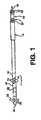
- FIG. 1is a plan view of one type of cardiac pacing lead in which the invention may usefully be practiced.
- the leadis an endocardial pacing lead provided with an elongated insulative outer sheath 10 which carries two mutually insulated conductors 12 and 13, illustrated schematically.
- an in-line bipolar connector assembly 14which may correspond to the IS-1 connector standard.
- Connector assembly 14is provided with a connector ring 16 coupled to conductor 12 and a connector pin 18 coupled to conductor 13.
- Sealing rings 20 and 22are provided to seal the connector assembly within the bore of an associated cardiac pacemaker and to prevent fluid leakage between connector ring 16 and connector pin 18.
- Pacing cathode 24may be any known type of pacing cathode employed in the context of cardiac pacing leads, however, it is illustrated as taking the general form of an endocardial pacing electrode.
- Tines 26are optionally provided to assist in stabilizing electrode 24 adjacent heart tissue. The invention may be practiced with any other type of endocardial electrodes such as active fixation helical or hook type electrodes.
- the lead of Figure. 1is merely exemplary, and that the invention is believed useful in conjunction with any type of implantable stimulation electrode, including epicardial pacing electrodes as described, for example, in U.S. Pat. No. 5,545,207 issued to Smits et al. , myocardial electrodes as described, for example, in U.S. Pat. No. 5,397,343 issued to Smits , and defibrillation electrodes as described, for example, in U.S. Pat. No. 5,016,645 issued to Williams et al. and U.S. Pat. No. 4,934,049 issued to Kiekhafer et al.
- the inventionmay also be useful in the field of muscle and nerve stimulation electrodes as disclosed, for example, in U.S. Pat. No. 4,735,205 issued to Chachques et al. and U.S. Pat. No. 5,265,608 issued to Lee et al.
- the present inventionmay also be applied to subcutaneous types of electrodes or "can” or “case” electrodes incorporated in the housing of an implantable medical device.
- the provision of a RuOx coating to achieve improved electrical performanceis believed to be beneficial in the context of all of these various implantable stimulation electrode types.
- Figure 2is a flow chart summarizing steps included in a method for manufacturing an electrode having a RuOx coating. While the embodiments described herein specify the use of RuOx, it is recognized that other metal oxide coatings may achieve similar benefits in improving the electrical properties of an implantable stimulation electrode. Other oxide layer coatings may be formed from metals such as titanium, vanadium, zirconium, niobium, molybdenum, tantalum, iridium, platinum, and tungsten. The methods described for depositing a RuOx coating may therefore be similarly applied for depositing said other metal oxide coatings on implantable stimulation electrodes.
- Method 50 for fabricating a RuOx coated electrodemay be applied to a variety of electrode substrate materials, such as titanium, platinum, platinum-iridium or niobium.
- electrode substrate materialssuch as titanium, platinum, platinum-iridium or niobium.
- the inventorshave found that the RuOx coating develops an enhanced structure when the electrode substrate has been roughened prior to depositing the RuOx coating.
- the enhanced structure of the RuOx coatingresults in a uniform surface and an increased surface area that is expected to enhance the overall improvement in the electrical performance of the stimulation electrode.
- the electrode substrateis roughened at step 55.
- Mechanical or chemical techniquescan be used to roughen the substrate surface.
- grit blastingis used to mechanically roughen the substrate surface using an alumina oxide media.
- the substrateis cleaned and dried at step 60.
- the substratemay be cleaned using ultrasonic techniques. In experiments performed by the inventors, a grit blasted electrode substrate was cleaned ultrasonically in acetone and then in isopropyl alcohol for five minutes each and then blown dry.
- an adhesion layerPrior to depositing the RuOx coating, an adhesion layer is applied over the roughened electrode substrate at step 65.
- an oxide layerwill spontaneously form over the electrode surface upon exposure to air. The presence of this oxide layer is expected to be the cause of delamination of a RuOx coating when the electrode is exposed to biphasic loads.
- an adhesion layeris applied to the electrode substrate in a vacuum to eliminate the effects of the spontaneous oxide layer. Titanium or zirconium is used for forming the adhesion layer.
- the adhesion layermay be about 500-1500 Angstroms in thickness, though other thicknesses greater than or less than this range may be effective in promoting strong adhesion of the RuOx coating. Addition of the Ti adhesion layer prevented delamination of a RuOx coated electrode under biphasic loads. The adhesion layer did not alter the final electrical properties of the RuOx coated electrode.
- ion-etchingmay be performed to remove the spontaneous oxide layer from the electrode substrate in addition to applying an adhesion layer.
- the RuOx coatingis deposited without exposing the electrode substrate to air to prevent the spontaneous oxide layer from reforming.
- the RuOx coatingis deposited.
- Deposition of the RuOx coatingis performed during a sputtering process in which sputtering parameters are optimized to achieve the greatest improvement in electrical properties of the electrode.
- the sputtering conditions that are controlled at optimized levels to achieve the greatest improvement in electrical properties of the electrodeinclude target power 72, total sputtering pressure 76, and the ratio of oxygen to argon in the sputter gas 74.
- the inventorshave optimized the sputtering parameters 72, 74 and 76 in a designed experiment
- Practice of the present inventionis, therefore, not limited to any particular sputter parameter setting but is directed toward using the optimal sputter parameter settings identified for a particular sputtering system that results in the greatest improvement in electrical properties (greatest reduction in post-pulse polarization).
- the sputtering timewill determine the RuOx coating thickness.
- a thickness of about 1 to 15 micronsmay be deposited, however practice of the present invention is not limited to a particular coating thickness.
- Capacitance measurements of RuOx coatings deposited on a titanium substrateshowed that capacitance increased as the RuOx coating increased.
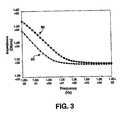
- Figures 3 and 4illustrate the benefit of optimizing sputtering parameters for improving electrode properties.
- Figure 3is a graph of frequency-dependent impedance measured for RuOx coated PtIr electrodes.
- Square data points 80correspond to impedance measurements made from a PtIr electrode coated with RuOx at a low sputtering target power setting.
- Triangular data points 82correspond to impedance measurements made from a PtIr electrode coated with RuOx at a high sputtering target power setting.
- Lower impedances 82were measured for the electrode coated with RuOx at a high sputtering power compared to the impedances 80 measured for the an electrode coated with RuOx at a low sputtering power.
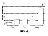
- Figure 4is a graph of post-pulse polarization measured for RuOx coated PtIr electrodes. Five levels of target power were tested to determine the optimal power setting. The highest power setting 84, shown at the far left, resulted in the lowest post-pulse polarization voltage and the lowest power setting 86, shown at the far right, resulted in the highest post-pulse polarization. Longer sputtering times were used for lower power settings to achieve a coating thickness of about 10 microns for all test electrodes. A thickness of about 10 microns was chosen for preparing test electrodes, however, other coating thicknesses can be beneficial in improving electrode properties.
Landscapes
- Health & Medical Sciences (AREA)
- Chemical & Material Sciences (AREA)
- Engineering & Computer Science (AREA)
- Public Health (AREA)
- Cardiology (AREA)
- Nuclear Medicine, Radiotherapy & Molecular Imaging (AREA)
- Radiology & Medical Imaging (AREA)
- Life Sciences & Earth Sciences (AREA)
- Animal Behavior & Ethology (AREA)
- General Health & Medical Sciences (AREA)
- Heart & Thoracic Surgery (AREA)
- Veterinary Medicine (AREA)
- Biomedical Technology (AREA)
- Inorganic Chemistry (AREA)
- Chemical Kinetics & Catalysis (AREA)
- Materials Engineering (AREA)
- Mechanical Engineering (AREA)
- Metallurgy (AREA)
- Organic Chemistry (AREA)
- Electrotherapy Devices (AREA)
- Physical Vapour Deposition (AREA)
Abstract
Description
- The present invention relates to implantable stimulation electrodes generally and more particularly to implantable stimulation electrodes fabricated to reduce post pulse polarization.
- Following delivery of a cardiac pacing pulse by an electrode, an after-potential typically remains on the electrode which persists for a sufficient period of time thereafter, that can interfere with sensing of cardiac signals associated with tissue depolarization caused by the delivered pulse. This phenomenon has been addressed in a number of ways over the years, and quite a large variety of electrode coatings have been developed in an effort to reduce post pulse polarization effects. One of the most common approaches to reducing post pulse polarization is to provide a high surface area coating having micron or sub-micron size surface features, such as a porous sintered metallic coating as described in
U.S. Pat. No. 4,280,514 issued to MacGregor , a metal oxide or nitride coating as described inU.S. Pat. No. 4,679,572 issued to Baker ,U.S. Pat. No. 5,571,158 issued to Bolz et al. andU.S. Pat. No. 5,683,443 issued to Munshi et al., or a coating of platinum black, as described inU.S. Pat. No. 4,502,492 issued to Bomzin ,U.S. Pat. No. 4,506,680 issued to Stokes ,U.S. Pat. No. 5,282,844 also issued to Stokes , andWO 2004/073790 . Furthermore, a platinum gray coating is known fromUS 2004/0220652 . - As noted in these patents, the provision of a high surface area coating does substantially lower post pulse polarization levels. However, as a practical matter, further reduction in post pulse polarization levels is still desirable.
- The present invention is as defined in claims 1 and 11. In particular, the invention is directed toward providing a low post-pulse polarization electrode having an increased surface area created by depositing a coating of e.g. ruthenium oxide (RuOx) on the electrode surface. Sputtering conditions during RuOx deposition are optimized to achieve the lowest post-pulse polarization and frequency dependent impedance response. Sputtering conditions that are optimized include target power, sputtering pressure and sputtering gas ratio.
- In one embodiment, the electrode substrate is roughened and cleaned prior to applying the RuOx coating using mechanical roughening by grit blasting with an alumina oxide media. The roughened substrate is ultrasonically cleaned. The method for fabricating a low post-pulse polarization electrode includes applying an adhesion layer to the electrode surface prior to depositing the RuOx coating to prevent delamination of the RuOx coating. The adhesion layer is formed of titanium (Ti) or zirconium (Zr) and applied in a vacuum environment to prevent oxidation of the adhesion layer surface. In an embodiment, the electrode substrate is ion etched to remove the spontaneous oxide film that forms over the electrode substrate and the RuOx coating is deposited
Figure 1 is a plan view of one type of cardiac pacing lead in which the invention may usefully be practiced.Figure 2 is a flow chart summarizing steps included in a method for manufacturing an electrode having a RuOx coating.Figure 3 is a graph of frequency-dependent impedance measured for RuOx coated PtIr electrodes.Figure 4 is a graph of post-pulse polarization measured for RuOx coated PtIr electrodes.Figure 1 is a plan view of one type of cardiac pacing lead in which the invention may usefully be practiced. In the case ofFigure 1 , the lead is an endocardial pacing lead provided with an elongated insulativeouter sheath 10 which carries two mutually insulated conductors 12 and 13, illustrated schematically. At the proximal end of the lead is an in-line bipolar connector assembly 14 which may correspond to the IS-1 connector standard. Connector assembly 14 is provided with a connector ring 16 coupled to conductor 12 and a connector pin 18 coupled to conductor 13.Sealing rings 20 and 22 are provided to seal the connector assembly within the bore of an associated cardiac pacemaker and to prevent fluid leakage between connector ring 16 and connector pin 18.- The proximal end of the lead carries a pacing cathode 24 and a pacing anode 28. Pacing cathode 24 may be any known type of pacing cathode employed in the context of cardiac pacing leads, however, it is illustrated as taking the general form of an endocardial pacing electrode. Tines 26 are optionally provided to assist in stabilizing electrode 24 adjacent heart tissue. The invention may be practiced with any other type of endocardial electrodes such as active fixation helical or hook type electrodes.
- It should be understood in the context of the present invention that the lead of
Figure. 1 is merely exemplary, and that the invention is believed useful in conjunction with any type of implantable stimulation electrode, including epicardial pacing electrodes as described, for example, inU.S. Pat. No. 5,545,207 issued to Smits et al. , myocardial electrodes as described, for example, inU.S. Pat. No. 5,397,343 issued to Smits , and defibrillation electrodes as described, for example, inU.S. Pat. No. 5,016,645 issued to Williams et al. andU.S. Pat. No. 4,934,049 issued to Kiekhafer et al. The invention may also be useful in the field of muscle and nerve stimulation electrodes as disclosed, for example, inU.S. Pat. No. 4,735,205 issued to Chachques et al. andU.S. Pat. No. 5,265,608 issued to Lee et al. - The present invention may also be applied to subcutaneous types of electrodes or "can" or "case" electrodes incorporated in the housing of an implantable medical device. The provision of a RuOx coating to achieve improved electrical performance is believed to be beneficial in the context of all of these various implantable stimulation electrode types.
Figure 2 is a flow chart summarizing steps included in a method for manufacturing an electrode having a RuOx coating. While the embodiments described herein specify the use of RuOx, it is recognized that other metal oxide coatings may achieve similar benefits in improving the electrical properties of an implantable stimulation electrode. Other oxide layer coatings may be formed from metals such as titanium, vanadium, zirconium, niobium, molybdenum, tantalum, iridium, platinum, and tungsten. The methods described for depositing a RuOx coating may therefore be similarly applied for depositing said other metal oxide coatings on implantable stimulation electrodes.Method 50 for fabricating a RuOx coated electrode may be applied to a variety of electrode substrate materials, such as titanium, platinum, platinum-iridium or niobium. The inventors have found that the RuOx coating develops an enhanced structure when the electrode substrate has been roughened prior to depositing the RuOx coating. The enhanced structure of the RuOx coating results in a uniform surface and an increased surface area that is expected to enhance the overall improvement in the electrical performance of the stimulation electrode.- As such, the electrode substrate is roughened at
step 55. Mechanical or chemical techniques can be used to roughen the substrate surface. In an exemplary embodiment, grit blasting is used to mechanically roughen the substrate surface using an alumina oxide media. After roughening the surface, the substrate is cleaned and dried atstep 60. The substrate may be cleaned using ultrasonic techniques. In experiments performed by the inventors, a grit blasted electrode substrate was cleaned ultrasonically in acetone and then in isopropyl alcohol for five minutes each and then blown dry. - Prior to depositing the RuOx coating, an adhesion layer is applied over the roughened electrode substrate at
step 65. During electrode fabrication, an oxide layer will spontaneously form over the electrode surface upon exposure to air. The presence of this oxide layer is expected to be the cause of delamination of a RuOx coating when the electrode is exposed to biphasic loads. In order to promote stronger RuOx coating adhesion, an adhesion layer is applied to the electrode substrate in a vacuum to eliminate the effects of the spontaneous oxide layer. Titanium or zirconium is used for forming the adhesion layer. The adhesion layer may be about 500-1500 Angstroms in thickness, though other thicknesses greater than or less than this range may be effective in promoting strong adhesion of the RuOx coating. Addition of the Ti adhesion layer prevented delamination of a RuOx coated electrode under biphasic loads. The adhesion layer did not alter the final electrical properties of the RuOx coated electrode. - In an alternative method, ion-etching may be performed to remove the spontaneous oxide layer from the electrode substrate in addition to applying an adhesion layer. After ion-etching, the RuOx coating is deposited without exposing the electrode substrate to air to prevent the spontaneous oxide layer from reforming.
- At
step 70 the RuOx coating is deposited. Deposition of the RuOx coating is performed during a sputtering process in which sputtering parameters are optimized to achieve the greatest improvement in electrical properties of the electrode. The sputtering conditions that are controlled at optimized levels to achieve the greatest improvement in electrical properties of the electrode includetarget power 72,total sputtering pressure 76, and the ratio of oxygen to argon in thesputter gas 74. The inventors have optimized thesputtering parameters - The effects of five levels of
target power 72, three levels ofsputter pressure 76 and three levels of oxygen toargon ratio 74 in the sputter gas on RuOx deposition rate and final electrical properties were measured. The highest deposition rate was achieved at a power setting of 300 Watts and was associated with the highest capacitance and lowest post-pulse polarization. Effects of sputtering pressure and gas ratio on electrical properties were less significant than the power setting, however the optimal settings tested were 9 millitorr sputtering pressure and 25% ratio of oxygen to argon in the sputter gas. In other sputtering systems, the optimal settings for the sputtering parameters for achieving optimal electrical properties may vary from these specified settings. Practice of the present invention is, therefore, not limited to any particular sputter parameter setting but is directed toward using the optimal sputter parameter settings identified for a particular sputtering system that results in the greatest improvement in electrical properties (greatest reduction in post-pulse polarization). - The sputtering time will determine the RuOx coating thickness. A thickness of about 1 to 15 microns may be deposited, however practice of the present invention is not limited to a particular coating thickness. Capacitance measurements of RuOx coatings deposited on a titanium substrate showed that capacitance increased as the RuOx coating increased.
Figures 3 and4 illustrate the benefit of optimizing sputtering parameters for improving electrode properties.Figure 3 is a graph of frequency-dependent impedance measured for RuOx coated PtIr electrodes. Square data points 80 correspond to impedance measurements made from a PtIr electrode coated with RuOx at a low sputtering target power setting. Triangular data points 82 correspond to impedance measurements made from a PtIr electrode coated with RuOx at a high sputtering target power setting.Lower impedances 82 were measured for the electrode coated with RuOx at a high sputtering power compared to theimpedances 80 measured for the an electrode coated with RuOx at a low sputtering power.Figure 4 is a graph of post-pulse polarization measured for RuOx coated PtIr electrodes. Five levels of target power were tested to determine the optimal power setting. The highest power setting 84, shown at the far left, resulted in the lowest post-pulse polarization voltage and the lowest power setting 86, shown at the far right, resulted in the highest post-pulse polarization. Longer sputtering times were used for lower power settings to achieve a coating thickness of about 10 microns for all test electrodes. A thickness of about 10 microns was chosen for preparing test electrodes, however, other coating thicknesses can be beneficial in improving electrode properties.- Thus, methods for fabricating a low impedance, low-polarization electrode having a well-adhered metal oxide coating have been described. Application of the methods described herein may benefit numerous types of implantable electrical devices, and therefore the exemplary embodiments described should not be considered limiting with regard to the following claims.
Claims (13)
- A method for fabricating an implantable electrode, comprising:providing an electrode substrate;roughening said substrate surface;cleaning the roughened surface;applying an adhesion layer formed of titanium or zirconium to the roughened and cleaned surface; and then depositing a metal oxide coating over the adhesion layer, the metal oxide comprising one of an oxide of titanium, vanadium, zirconium, niobium, molybdenum, tantalum, iridium, platinum, tungsten or ruthenium; wherein the step of depositing the metal oxide coating comprises sputtering the metal, forming the oxide, onto the adhesion layer using sputtering process parameters optimized to minimize post-pulse polarization.
- The method of claim 1 wherein roughening the surface of the electrode comprises mechanical roughening of the electrode surface.
- The method of claim 2 wherein the mechanical roughening of the electrode surface comprises grit blasting.
- The method of claim 3 wherein the grit blasting is performed using an alumina oxide media.
- The method of claim 1 wherein the cleaning of the roughened electrode surface comprises ultrasonic cleaning.
- The method of claim 1 wherein the sputtering process parameters, optimized to minimize post-pulse polarization, include a target power.
- The method of claim 7 wherein the target power is 300 Watts.
- The method of claim 1 wherein the sputtering parameters optimized to minimize post-pulse polarization include a sputtering pressure.
- The method of claim 1 wherein the sputtering parameters optimized to minimize post-pulse polarization include a sputtering gas ratio.
- The method of claim 1 further comprising ion-etching the roughened electrode surface prior to depositing the metal oxide layer.
- An implantable medical electrode, comprising:a roughened electrode substrate,an adhesion layer formed of titanium or zirconium covering at least a portion of the roughened electrode substrate, anda metal oxide coating covering the adhesion layer to minimize post-pulse polarization voltage of the electrode, the metal oxide comprising one of an oxide of titanium, vanadium, zirconium, niobium, molybdenum, tantalum, iridium, platinum, tungsten or ruthenium;
- The electrode of claim 12 wherein the adhesion layer being between 500 and 1500 angstroms in thickness.
- The electrode of claim 14 wherein the metal oxide coating is 1-15 microns in thickness.
Applications Claiming Priority (2)
| Application Number | Priority Date | Filing Date | Title |
|---|---|---|---|
| US11/042,649US8155754B2 (en) | 2005-01-25 | 2005-01-25 | Method for fabrication of low-polarization implantable stimulation electrode |
| PCT/US2006/002737WO2006081344A1 (en) | 2005-01-25 | 2006-01-25 | Method for fabrication of low-polarization implantable stimulation electrode |
Publications (2)
| Publication Number | Publication Date |
|---|---|
| EP1848495A1 EP1848495A1 (en) | 2007-10-31 |
| EP1848495B1true EP1848495B1 (en) | 2009-11-25 |
Family
ID=36423506
Family Applications (1)
| Application Number | Title | Priority Date | Filing Date |
|---|---|---|---|
| EP06719552ACeasedEP1848495B1 (en) | 2005-01-25 | 2006-01-25 | Method for fabrication of low-polarization implantable stimulation electrode |
Country Status (7)
| Country | Link |
|---|---|
| US (3) | US8155754B2 (en) |
| EP (1) | EP1848495B1 (en) |
| JP (1) | JP2008528189A (en) |
| AT (1) | ATE449631T1 (en) |
| CA (1) | CA2594480A1 (en) |
| DE (1) | DE602006010664D1 (en) |
| WO (1) | WO2006081344A1 (en) |
Families Citing this family (34)
| Publication number | Priority date | Publication date | Assignee | Title |
|---|---|---|---|---|
| US8155754B2 (en) | 2005-01-25 | 2012-04-10 | Medtronic, Inc. | Method for fabrication of low-polarization implantable stimulation electrode |
| US7610101B2 (en)* | 2006-11-30 | 2009-10-27 | Cardiac Pacemakers, Inc. | RF rejecting lead |
| US8996129B2 (en)* | 2007-01-31 | 2015-03-31 | Medtronic, Inc. | Medical electrode including an iridium oxide surface and methods of fabrication |
| US7706891B2 (en)* | 2007-03-21 | 2010-04-27 | St. Jude Medical, Atrial Fibrillation Division, Inc. | Catheter employing shape memory alloy shaping wire or pull wire and method of its manufacture |
| AU2008335462B2 (en)* | 2007-12-06 | 2014-02-20 | Cardiac Pacemakers, Inc. | Implantable lead having a variable coil conductor pitch |
| WO2009100003A1 (en)* | 2008-02-06 | 2009-08-13 | Cardiac Pacemakers, Inc. | Lead with mri compatible design features |
| US8103360B2 (en)* | 2008-05-09 | 2012-01-24 | Foster Arthur J | Medical lead coil conductor with spacer element |
| CN102292053A (en) | 2008-09-29 | 2011-12-21 | 卡迪尔克阀门技术公司 | Heart valve |
| WO2010040009A1 (en) | 2008-10-01 | 2010-04-08 | Cardiaq Valve Technologies, Inc. | Delivery system for vascular implant |
| US9084883B2 (en)* | 2009-03-12 | 2015-07-21 | Cardiac Pacemakers, Inc. | Thin profile conductor assembly for medical device leads |
| CA2961053C (en) | 2009-04-15 | 2019-04-30 | Edwards Lifesciences Cardiaq Llc | Vascular implant and delivery system |
| ES2547713T3 (en) | 2009-06-26 | 2015-10-08 | Cardiac Pacemakers, Inc. | Bypass of a medical device that includes a single-coil coil with improved torque transmission capacity and reduced RM heating |
| US8335572B2 (en) | 2009-10-08 | 2012-12-18 | Cardiac Pacemakers, Inc. | Medical device lead including a flared conductive coil |
| US9254380B2 (en) | 2009-10-19 | 2016-02-09 | Cardiac Pacemakers, Inc. | MRI compatible tachycardia lead |
| US9750944B2 (en) | 2009-12-30 | 2017-09-05 | Cardiac Pacemakers, Inc. | MRI-conditionally safe medical device lead |
| WO2011081713A1 (en) | 2009-12-31 | 2011-07-07 | Cardiac Pacemakers, Inc. | Mri conditionally safe lead with multi-layer conductor |
| US8391994B2 (en) | 2009-12-31 | 2013-03-05 | Cardiac Pacemakers, Inc. | MRI conditionally safe lead with low-profile multi-layer conductor for longitudinal expansion |
| US8579964B2 (en) | 2010-05-05 | 2013-11-12 | Neovasc Inc. | Transcatheter mitral valve prosthesis |
| US8825181B2 (en) | 2010-08-30 | 2014-09-02 | Cardiac Pacemakers, Inc. | Lead conductor with pitch and torque control for MRI conditionally safe use |
| US9554897B2 (en) | 2011-04-28 | 2017-01-31 | Neovasc Tiara Inc. | Methods and apparatus for engaging a valve prosthesis with tissue |
| US9308087B2 (en) | 2011-04-28 | 2016-04-12 | Neovasc Tiara Inc. | Sequentially deployed transcatheter mitral valve prosthesis |
| US8666512B2 (en) | 2011-11-04 | 2014-03-04 | Cardiac Pacemakers, Inc. | Implantable medical device lead including inner coil reverse-wound relative to shocking coil |
| AU2013249088B2 (en) | 2012-04-20 | 2015-12-03 | Cardiac Pacemakers, Inc. | Implantable medical device lead including a unifilar coiled cable |
| US9345573B2 (en) | 2012-05-30 | 2016-05-24 | Neovasc Tiara Inc. | Methods and apparatus for loading a prosthesis onto a delivery system |
| US8954168B2 (en) | 2012-06-01 | 2015-02-10 | Cardiac Pacemakers, Inc. | Implantable device lead including a distal electrode assembly with a coiled component |
| JP6069499B2 (en) | 2012-08-31 | 2017-02-01 | カーディアック ペースメイカーズ, インコーポレイテッド | Lead wire with low peak MRI heating |
| US8983623B2 (en) | 2012-10-18 | 2015-03-17 | Cardiac Pacemakers, Inc. | Inductive element for providing MRI compatibility in an implantable medical device lead |
| US10583002B2 (en) | 2013-03-11 | 2020-03-10 | Neovasc Tiara Inc. | Prosthetic valve with anti-pivoting mechanism |
| US9681951B2 (en) | 2013-03-14 | 2017-06-20 | Edwards Lifesciences Cardiaq Llc | Prosthesis with outer skirt and anchors |
| US10493265B2 (en) | 2013-03-15 | 2019-12-03 | Medtronic, Inc. | Medical leads and techniques for manufacturing the same |
| US10406349B2 (en)* | 2013-03-15 | 2019-09-10 | Medtronic, Inc. | Medical leads and techniques for manufacturing the same |
| US9572665B2 (en) | 2013-04-04 | 2017-02-21 | Neovasc Tiara Inc. | Methods and apparatus for delivering a prosthetic valve to a beating heart |
| WO2015130753A1 (en) | 2014-02-26 | 2015-09-03 | Cardiac Pacemakers, Inc | Construction of an mri-safe tachycardia lead |
| WO2020240193A1 (en)* | 2019-05-31 | 2020-12-03 | Johnson Matthey Public Limited Company | Thin film coating |
Family Cites Families (67)
| Publication number | Priority date | Publication date | Assignee | Title |
|---|---|---|---|---|
| US3975557A (en)* | 1975-01-02 | 1976-08-17 | The Dow Chemical Company | Producing an electrode |
| US4280514A (en)* | 1975-05-09 | 1981-07-28 | Macgregor David C | Endocardial pacemaker electrode |
| US4408604A (en)* | 1981-04-06 | 1983-10-11 | Teletronics Pty, Limited | Porous pacemaker electrode tip |
| US4506680A (en)* | 1983-03-17 | 1985-03-26 | Medtronic, Inc. | Drug dispensing body implantable lead |
| US4502492A (en)* | 1983-04-28 | 1985-03-05 | Medtronic, Inc. | Low-polarization low-threshold electrode |
| US4649937A (en) | 1985-01-28 | 1987-03-17 | Cordis Corporation | Etched grooved electrode for pacing lead and method for making same |
| US4717581A (en) | 1986-02-06 | 1988-01-05 | Eic Laboratories, Inc. | Iridium oxide coated electrodes for neural stimulation |
| US4677989A (en) | 1986-02-06 | 1987-07-07 | Eic Laboratories, Inc. | Iridium oxide coated electrodes for neural stimulation |
| US4735205A (en)* | 1986-02-24 | 1988-04-05 | Medtronic, Inc. | Method and apparatus including a sliding insulation lead for cardiac assistance |
| US4679572A (en)* | 1986-03-11 | 1987-07-14 | Intermedics, Inc. | Low threshold cardiac pacing electrodes |
| US4762136A (en) | 1987-02-19 | 1988-08-09 | Intermedics, Inc. | Low polarization pacing electrodes for capture verification |
| CA1305528C (en) | 1986-03-11 | 1992-07-21 | Ross G. Baker, Jr. | Low threshold cardiac pacing electrodes |
| US4784160A (en)* | 1986-08-19 | 1988-11-15 | Cordis Corporation | Implantable device having plasma sprayed ceramic porous surface |
| US5016645A (en)* | 1987-06-18 | 1991-05-21 | Terrell Williams | Medical electrode lead |
| US4860446A (en) | 1988-02-16 | 1989-08-29 | Medtronic, Inc. | Medical electrical lead and method of manufacture |
| US4919135A (en) | 1988-12-14 | 1990-04-24 | Intermedics, Inc. | Triaxial electrode |
| US5074313A (en)* | 1989-03-20 | 1991-12-24 | Cardiac Pacemakers, Inc. | Porous electrode with enhanced reactive surface |
| US4934049A (en)* | 1989-07-07 | 1990-06-19 | Medtronic, Inc. | Method for fabrication of a medical electrode |
| US5265608A (en)* | 1990-02-22 | 1993-11-30 | Medtronic, Inc. | Steroid eluting electrode for peripheral nerve stimulation |
| US5097843A (en) | 1990-04-10 | 1992-03-24 | Siemens-Pacesetter, Inc. | Porous electrode for a pacemaker |
| US5181526A (en)* | 1990-04-20 | 1993-01-26 | Tanaka Kikinzoku Kogyo K.K. | Electrode for human heart pacemaker |
| US5314458A (en) | 1990-06-01 | 1994-05-24 | University Of Michigan | Single channel microstimulator |
| US5203348A (en)* | 1990-06-06 | 1993-04-20 | Cardiac Pacemakers, Inc. | Subcutaneous defibrillation electrodes |
| US5282844A (en)* | 1990-06-15 | 1994-02-01 | Medtronic, Inc. | High impedance, low polarization, low threshold miniature steriod eluting pacing lead electrodes |
| DE4207368A1 (en)* | 1991-08-06 | 1993-02-11 | Biotronik Mess & Therapieg | VOICE ELECTRODE |
| US5318572A (en) | 1992-06-02 | 1994-06-07 | Siemens Pacesetter, Inc. | High efficiency tissue stimulating and signal sensing electrode |
| US5326448A (en) | 1992-10-15 | 1994-07-05 | Telectronics Pacing Systems, Inc. | Method for reducing the polarization of bioelectrical stimulation leads using surface enhancement, and product made thereby |
| AU5214193A (en)* | 1992-12-03 | 1994-06-16 | Pacesetter Ab | Implantable medical device lead assembly having high efficiency, flexible electrode head |
| US5344494A (en)* | 1993-01-21 | 1994-09-06 | Smith & Nephew Richards, Inc. | Method for cleaning porous and roughened surfaces on medical implants |
| US5397343A (en)* | 1993-12-09 | 1995-03-14 | Medtronic, Inc. | Medical electrical lead having counter fixation anchoring system |
| US5545207A (en)* | 1994-08-24 | 1996-08-13 | Medtronic, Inc. | Medical electrical lead having stable fixation system |
| DE4440386A1 (en) | 1994-11-11 | 1996-05-15 | Pacesetter Ab | Electrodes for medical applications |
| US5534022A (en)* | 1994-11-22 | 1996-07-09 | Ventritex, Inc. | Lead having an integrated defibrillation/sensing electrode |
| US5683443A (en)* | 1995-02-07 | 1997-11-04 | Intermedics, Inc. | Implantable stimulation electrodes with non-native metal oxide coating mixtures |
| US5654030A (en) | 1995-02-07 | 1997-08-05 | Intermedics, Inc. | Method of making implantable stimulation electrodes |
| US5759932A (en)* | 1996-11-08 | 1998-06-02 | General Electric Company | Coating composition for metal-based substrates, and related processes |
| US5920455A (en) | 1997-05-01 | 1999-07-06 | Wilson Greatbatch Ltd. | One step ultrasonically coated substrate for use in a capacitor |
| US6253110B1 (en)* | 1999-04-27 | 2001-06-26 | Medtronic Inc | Method for tissue stimulation and fabrication of low polarization implantable stimulation electrode |
| US6799076B2 (en)* | 1999-12-07 | 2004-09-28 | Greatbatch-Hittman, Inc. | Coated electrode and method of making a coated electrode |
| US6908624B2 (en)* | 1999-12-23 | 2005-06-21 | Advanced Cardiovascular Systems, Inc. | Coating for implantable devices and a method of forming the same |
| US20050238686A1 (en)* | 1999-12-23 | 2005-10-27 | Advanced Cardiovascular Systems, Inc. | Coating for implantable devices and a method of forming the same |
| AUPR090300A0 (en) | 2000-10-20 | 2000-11-16 | AMC Technologies Pty Limited | An electrical lead |
| US6430448B1 (en) | 2000-11-07 | 2002-08-06 | Pacesetter, Inc. | Stimulating electrode having low polarization and method of making same |
| US6430447B1 (en) | 2000-11-07 | 2002-08-06 | Pacesetter, Inc. | Stimulating electrode having low polarization and method of making same |
| US7005404B2 (en)* | 2000-12-20 | 2006-02-28 | Honda Motor Co., Ltd. | Substrates with small particle size metal oxide and noble metal catalyst coatings and thermal spraying methods for producing the same |
| US20040240152A1 (en)* | 2003-05-30 | 2004-12-02 | Schott Joachim Hossick | Capacitor and method for producing a capacitor |
| US7103418B2 (en)* | 2002-10-02 | 2006-09-05 | Medtronic, Inc. | Active fluid delivery catheter |
| US7844347B2 (en) | 2002-12-06 | 2010-11-30 | Medtronic, Inc. | Medical devices incorporating carbon nanotube material and methods of fabricating same |
| US20050075709A1 (en) | 2003-02-18 | 2005-04-07 | Medtronic, Inc. | Biomedical electrode of enhanced surface area |
| ATE442181T1 (en)* | 2003-03-03 | 2009-09-15 | Greatbatch Ltd | LOW POLARIZATION COATINGS FOR IMPLANTABLE ELECTRODES |
| US7571011B2 (en) | 2003-05-01 | 2009-08-04 | Second Sight Medical Products, Inc. | Adherent metal oxide coating forming a high surface area electrode |
| JP4997688B2 (en) | 2003-08-19 | 2012-08-08 | セイコーエプソン株式会社 | Electrode, thin film transistor, electronic circuit, display device and electronic device |
| US7945337B2 (en) | 2003-08-27 | 2011-05-17 | Medtronic, Inc. | High impedance and low polarization electrode |
| US20050048876A1 (en)* | 2003-09-02 | 2005-03-03 | Applied Materials, Inc. | Fabricating and cleaning chamber components having textured surfaces |
| US7566389B2 (en)* | 2003-10-08 | 2009-07-28 | Akzo Nobel N.V. | Electrode |
| US8017178B2 (en)* | 2003-12-16 | 2011-09-13 | Cardiac Pacemakers, Inc. | Coatings for implantable electrodes |
| US7463917B2 (en) | 2004-04-28 | 2008-12-09 | Medtronic, Inc. | Electrodes for sustained delivery of energy |
| US7022621B1 (en) | 2004-10-21 | 2006-04-04 | Sharp Laboratories Of America, Inc. | Iridium oxide nanostructure patterning |
| US7255745B2 (en) | 2004-10-21 | 2007-08-14 | Sharp Laboratories Of America, Inc. | Iridium oxide nanowires and method for forming same |
| US7098144B2 (en) | 2004-10-21 | 2006-08-29 | Sharp Laboratories Of America, Inc. | Iridium oxide nanotubes and method for forming same |
| US7208372B2 (en) | 2005-01-19 | 2007-04-24 | Sharp Laboratories Of America, Inc. | Non-volatile memory resistor cell with nanotip electrode |
| US8155754B2 (en)* | 2005-01-25 | 2012-04-10 | Medtronic, Inc. | Method for fabrication of low-polarization implantable stimulation electrode |
| US8229570B2 (en) | 2006-01-30 | 2012-07-24 | Medtronic, Inc. | Implantable electrodes having zirconium nitride coatings |
| WO2007134315A1 (en) | 2006-05-15 | 2007-11-22 | Cardiac Pacemakers, Inc. | Porous surface electrode for coronary venous applications |
| US8996129B2 (en) | 2007-01-31 | 2015-03-31 | Medtronic, Inc. | Medical electrode including an iridium oxide surface and methods of fabrication |
| US20080253922A1 (en)* | 2007-04-13 | 2008-10-16 | General Electric Company | Method for roughening metal surfaces and article manufactured thereby |
| CN101626846B (en)* | 2007-04-18 | 2011-12-14 | 德诺拉工业有限公司 | electrodes with mechanically roughened surface for electrochemical applications |
- 2005
- 2005-01-25USUS11/042,649patent/US8155754B2/ennot_activeExpired - Fee Related
- 2006
- 2006-01-25CACA002594480Apatent/CA2594480A1/ennot_activeAbandoned
- 2006-01-25DEDE602006010664Tpatent/DE602006010664D1/enactiveActive
- 2006-01-25WOPCT/US2006/002737patent/WO2006081344A1/enactiveApplication Filing
- 2006-01-25JPJP2007553222Apatent/JP2008528189A/enactivePending
- 2006-01-25EPEP06719552Apatent/EP1848495B1/ennot_activeCeased
- 2006-01-25ATAT06719552Tpatent/ATE449631T1/ennot_activeIP Right Cessation
- 2009
- 2009-12-17USUS12/640,610patent/US20100137963A1/ennot_activeAbandoned
- 2015
- 2015-06-18USUS14/743,838patent/US20150283375A1/ennot_activeAbandoned
Also Published As
| Publication number | Publication date |
|---|---|
| DE602006010664D1 (en) | 2010-01-07 |
| CA2594480A1 (en) | 2006-08-03 |
| EP1848495A1 (en) | 2007-10-31 |
| US20060167536A1 (en) | 2006-07-27 |
| JP2008528189A (en) | 2008-07-31 |
| US20150283375A1 (en) | 2015-10-08 |
| US20100137963A1 (en) | 2010-06-03 |
| US8155754B2 (en) | 2012-04-10 |
| WO2006081344A1 (en) | 2006-08-03 |
| ATE449631T1 (en) | 2009-12-15 |
Similar Documents
| Publication | Publication Date | Title |
|---|---|---|
| EP1848495B1 (en) | Method for fabrication of low-polarization implantable stimulation electrode | |
| US6799076B2 (en) | Coated electrode and method of making a coated electrode | |
| US6253110B1 (en) | Method for tissue stimulation and fabrication of low polarization implantable stimulation electrode | |
| US5654030A (en) | Method of making implantable stimulation electrodes | |
| US5683443A (en) | Implantable stimulation electrodes with non-native metal oxide coating mixtures | |
| US8017179B2 (en) | Coatings for implantable electrodes | |
| US5411544A (en) | Defibrillation lead with improved mechanical and electrical characteristics | |
| JP2574075B2 (en) | Implantable electrodes | |
| US20100125319A1 (en) | Cell-repelling polymeric electrode having a structured surface | |
| EP2922594B1 (en) | Medical electrodes with layered coatings | |
| US8948881B2 (en) | Method for producing implantable electrode coatings with a plurality of morphologies | |
| WO2007134315A1 (en) | Porous surface electrode for coronary venous applications | |
| US20150182743A1 (en) | Medical electrode including an iridium oxide surface and methods of fabrication | |
| US20050075709A1 (en) | Biomedical electrode of enhanced surface area | |
| US8229570B2 (en) | Implantable electrodes having zirconium nitride coatings | |
| US7459369B2 (en) | High capacitance low resistance electrode |
Legal Events
| Date | Code | Title | Description |
|---|---|---|---|
| PUAI | Public reference made under article 153(3) epc to a published international application that has entered the european phase | Free format text:ORIGINAL CODE: 0009012 | |
| 17P | Request for examination filed | Effective date:20070824 | |
| AK | Designated contracting states | Kind code of ref document:A1 Designated state(s):AT BE BG CH CY CZ DE DK EE ES FI FR GB GR HU IE IS IT LI LT LU LV MC NL PL PT RO SE SI SK TR | |
| 17Q | First examination report despatched | Effective date:20071217 | |
| DAX | Request for extension of the european patent (deleted) | ||
| GRAP | Despatch of communication of intention to grant a patent | Free format text:ORIGINAL CODE: EPIDOSNIGR1 | |
| GRAS | Grant fee paid | Free format text:ORIGINAL CODE: EPIDOSNIGR3 | |
| GRAA | (expected) grant | Free format text:ORIGINAL CODE: 0009210 | |
| AK | Designated contracting states | Kind code of ref document:B1 Designated state(s):AT BE BG CH CY CZ DE DK EE ES FI FR GB GR HU IE IS IT LI LT LU LV MC NL PL PT RO SE SI SK TR | |
| REG | Reference to a national code | Ref country code:GB Ref legal event code:FG4D | |
| REG | Reference to a national code | Ref country code:CH Ref legal event code:EP | |
| REG | Reference to a national code | Ref country code:IE Ref legal event code:FG4D | |
| REF | Corresponds to: | Ref document number:602006010664 Country of ref document:DE Date of ref document:20100107 Kind code of ref document:P | |
| REG | Reference to a national code | Ref country code:NL Ref legal event code:VDEP Effective date:20091125 | |
| LTIE | Lt: invalidation of european patent or patent extension | Effective date:20091125 | |
| PG25 | Lapsed in a contracting state [announced via postgrant information from national office to epo] | Ref country code:PT Free format text:LAPSE BECAUSE OF FAILURE TO SUBMIT A TRANSLATION OF THE DESCRIPTION OR TO PAY THE FEE WITHIN THE PRESCRIBED TIME-LIMIT Effective date:20100325 Ref country code:LT Free format text:LAPSE BECAUSE OF FAILURE TO SUBMIT A TRANSLATION OF THE DESCRIPTION OR TO PAY THE FEE WITHIN THE PRESCRIBED TIME-LIMIT Effective date:20091125 Ref country code:FI Free format text:LAPSE BECAUSE OF FAILURE TO SUBMIT A TRANSLATION OF THE DESCRIPTION OR TO PAY THE FEE WITHIN THE PRESCRIBED TIME-LIMIT Effective date:20091125 Ref country code:IS Free format text:LAPSE BECAUSE OF FAILURE TO SUBMIT A TRANSLATION OF THE DESCRIPTION OR TO PAY THE FEE WITHIN THE PRESCRIBED TIME-LIMIT Effective date:20100325 Ref country code:SE Free format text:LAPSE BECAUSE OF FAILURE TO SUBMIT A TRANSLATION OF THE DESCRIPTION OR TO PAY THE FEE WITHIN THE PRESCRIBED TIME-LIMIT Effective date:20091125 | |
| PG25 | Lapsed in a contracting state [announced via postgrant information from national office to epo] | Ref country code:PL Free format text:LAPSE BECAUSE OF FAILURE TO SUBMIT A TRANSLATION OF THE DESCRIPTION OR TO PAY THE FEE WITHIN THE PRESCRIBED TIME-LIMIT Effective date:20091125 Ref country code:SI Free format text:LAPSE BECAUSE OF FAILURE TO SUBMIT A TRANSLATION OF THE DESCRIPTION OR TO PAY THE FEE WITHIN THE PRESCRIBED TIME-LIMIT Effective date:20091125 Ref country code:CY Free format text:LAPSE BECAUSE OF FAILURE TO SUBMIT A TRANSLATION OF THE DESCRIPTION OR TO PAY THE FEE WITHIN THE PRESCRIBED TIME-LIMIT Effective date:20091125 Ref country code:LV Free format text:LAPSE BECAUSE OF FAILURE TO SUBMIT A TRANSLATION OF THE DESCRIPTION OR TO PAY THE FEE WITHIN THE PRESCRIBED TIME-LIMIT Effective date:20091125 | |
| PG25 | Lapsed in a contracting state [announced via postgrant information from national office to epo] | Ref country code:BE Free format text:LAPSE BECAUSE OF FAILURE TO SUBMIT A TRANSLATION OF THE DESCRIPTION OR TO PAY THE FEE WITHIN THE PRESCRIBED TIME-LIMIT Effective date:20091125 Ref country code:AT Free format text:LAPSE BECAUSE OF FAILURE TO SUBMIT A TRANSLATION OF THE DESCRIPTION OR TO PAY THE FEE WITHIN THE PRESCRIBED TIME-LIMIT Effective date:20091125 | |
| PG25 | Lapsed in a contracting state [announced via postgrant information from national office to epo] | Ref country code:ES Free format text:LAPSE BECAUSE OF FAILURE TO SUBMIT A TRANSLATION OF THE DESCRIPTION OR TO PAY THE FEE WITHIN THE PRESCRIBED TIME-LIMIT Effective date:20100308 Ref country code:RO Free format text:LAPSE BECAUSE OF FAILURE TO SUBMIT A TRANSLATION OF THE DESCRIPTION OR TO PAY THE FEE WITHIN THE PRESCRIBED TIME-LIMIT Effective date:20091125 Ref country code:EE Free format text:LAPSE BECAUSE OF FAILURE TO SUBMIT A TRANSLATION OF THE DESCRIPTION OR TO PAY THE FEE WITHIN THE PRESCRIBED TIME-LIMIT Effective date:20091125 Ref country code:DK Free format text:LAPSE BECAUSE OF FAILURE TO SUBMIT A TRANSLATION OF THE DESCRIPTION OR TO PAY THE FEE WITHIN THE PRESCRIBED TIME-LIMIT Effective date:20091125 Ref country code:BG Free format text:LAPSE BECAUSE OF FAILURE TO SUBMIT A TRANSLATION OF THE DESCRIPTION OR TO PAY THE FEE WITHIN THE PRESCRIBED TIME-LIMIT Effective date:20100225 Ref country code:NL Free format text:LAPSE BECAUSE OF FAILURE TO SUBMIT A TRANSLATION OF THE DESCRIPTION OR TO PAY THE FEE WITHIN THE PRESCRIBED TIME-LIMIT Effective date:20091125 | |
| PG25 | Lapsed in a contracting state [announced via postgrant information from national office to epo] | Ref country code:SK Free format text:LAPSE BECAUSE OF FAILURE TO SUBMIT A TRANSLATION OF THE DESCRIPTION OR TO PAY THE FEE WITHIN THE PRESCRIBED TIME-LIMIT Effective date:20091125 Ref country code:CZ Free format text:LAPSE BECAUSE OF FAILURE TO SUBMIT A TRANSLATION OF THE DESCRIPTION OR TO PAY THE FEE WITHIN THE PRESCRIBED TIME-LIMIT Effective date:20091125 Ref country code:MC Free format text:LAPSE BECAUSE OF NON-PAYMENT OF DUE FEES Effective date:20100131 | |
| REG | Reference to a national code | Ref country code:CH Ref legal event code:PL | |
| PLBE | No opposition filed within time limit | Free format text:ORIGINAL CODE: 0009261 | |
| STAA | Information on the status of an ep patent application or granted ep patent | Free format text:STATUS: NO OPPOSITION FILED WITHIN TIME LIMIT | |
| GBPC | Gb: european patent ceased through non-payment of renewal fee | Effective date:20100225 | |
| PG25 | Lapsed in a contracting state [announced via postgrant information from national office to epo] | Ref country code:LI Free format text:LAPSE BECAUSE OF NON-PAYMENT OF DUE FEES Effective date:20100131 Ref country code:CH Free format text:LAPSE BECAUSE OF NON-PAYMENT OF DUE FEES Effective date:20100131 Ref country code:GR Free format text:LAPSE BECAUSE OF FAILURE TO SUBMIT A TRANSLATION OF THE DESCRIPTION OR TO PAY THE FEE WITHIN THE PRESCRIBED TIME-LIMIT Effective date:20100226 | |
| 26N | No opposition filed | Effective date:20100826 | |
| PG25 | Lapsed in a contracting state [announced via postgrant information from national office to epo] | Ref country code:IE Free format text:LAPSE BECAUSE OF NON-PAYMENT OF DUE FEES Effective date:20100125 | |
| PG25 | Lapsed in a contracting state [announced via postgrant information from national office to epo] | Ref country code:IT Free format text:LAPSE BECAUSE OF FAILURE TO SUBMIT A TRANSLATION OF THE DESCRIPTION OR TO PAY THE FEE WITHIN THE PRESCRIBED TIME-LIMIT Effective date:20091125 Ref country code:GB Free format text:LAPSE BECAUSE OF NON-PAYMENT OF DUE FEES Effective date:20100225 | |
| PG25 | Lapsed in a contracting state [announced via postgrant information from national office to epo] | Ref country code:LU Free format text:LAPSE BECAUSE OF NON-PAYMENT OF DUE FEES Effective date:20100125 Ref country code:HU Free format text:LAPSE BECAUSE OF FAILURE TO SUBMIT A TRANSLATION OF THE DESCRIPTION OR TO PAY THE FEE WITHIN THE PRESCRIBED TIME-LIMIT Effective date:20100526 | |
| PG25 | Lapsed in a contracting state [announced via postgrant information from national office to epo] | Ref country code:TR Free format text:LAPSE BECAUSE OF FAILURE TO SUBMIT A TRANSLATION OF THE DESCRIPTION OR TO PAY THE FEE WITHIN THE PRESCRIBED TIME-LIMIT Effective date:20091125 | |
| REG | Reference to a national code | Ref country code:FR Ref legal event code:PLFP Year of fee payment:11 | |
| REG | Reference to a national code | Ref country code:FR Ref legal event code:PLFP Year of fee payment:12 | |
| REG | Reference to a national code | Ref country code:FR Ref legal event code:PLFP Year of fee payment:13 | |
| PGFP | Annual fee paid to national office [announced via postgrant information from national office to epo] | Ref country code:FR Payment date:20191219 Year of fee payment:15 | |
| PG25 | Lapsed in a contracting state [announced via postgrant information from national office to epo] | Ref country code:FR Free format text:LAPSE BECAUSE OF NON-PAYMENT OF DUE FEES Effective date:20210131 | |
| PGFP | Annual fee paid to national office [announced via postgrant information from national office to epo] | Ref country code:DE Payment date:20211215 Year of fee payment:17 | |
| REG | Reference to a national code | Ref country code:DE Ref legal event code:R119 Ref document number:602006010664 Country of ref document:DE | |
| PG25 | Lapsed in a contracting state [announced via postgrant information from national office to epo] | Ref country code:DE Free format text:LAPSE BECAUSE OF NON-PAYMENT OF DUE FEES Effective date:20230801 |