EP1845562A1 - Anti-reflective substrate and the manufacturing method thereof - Google Patents
Anti-reflective substrate and the manufacturing method thereofDownload PDFInfo
- Publication number
- EP1845562A1 EP1845562A1EP06252031AEP06252031AEP1845562A1EP 1845562 A1EP1845562 A1EP 1845562A1EP 06252031 AEP06252031 AEP 06252031AEP 06252031 AEP06252031 AEP 06252031AEP 1845562 A1EP1845562 A1EP 1845562A1
- Authority
- EP
- European Patent Office
- Prior art keywords
- substrate
- amorphous silicon
- reflective
- silicon layer
- etching
- Prior art date
- Legal status (The legal status is an assumption and is not a legal conclusion. Google has not performed a legal analysis and makes no representation as to the accuracy of the status listed.)
- Granted
Links
Images


Classifications
- H—ELECTRICITY
- H10—SEMICONDUCTOR DEVICES; ELECTRIC SOLID-STATE DEVICES NOT OTHERWISE PROVIDED FOR
- H10F—INORGANIC SEMICONDUCTOR DEVICES SENSITIVE TO INFRARED RADIATION, LIGHT, ELECTROMAGNETIC RADIATION OF SHORTER WAVELENGTH OR CORPUSCULAR RADIATION
- H10F77/00—Constructional details of devices covered by this subclass
- H10F77/30—Coatings
- H10F77/306—Coatings for devices having potential barriers
- G—PHYSICS
- G02—OPTICS
- G02B—OPTICAL ELEMENTS, SYSTEMS OR APPARATUS
- G02B1/00—Optical elements characterised by the material of which they are made; Optical coatings for optical elements
- G02B1/10—Optical coatings produced by application to, or surface treatment of, optical elements
- G02B1/11—Anti-reflection coatings
- G02B1/113—Anti-reflection coatings using inorganic layer materials only
- H—ELECTRICITY
- H10—SEMICONDUCTOR DEVICES; ELECTRIC SOLID-STATE DEVICES NOT OTHERWISE PROVIDED FOR
- H10F—INORGANIC SEMICONDUCTOR DEVICES SENSITIVE TO INFRARED RADIATION, LIGHT, ELECTROMAGNETIC RADIATION OF SHORTER WAVELENGTH OR CORPUSCULAR RADIATION
- H10F71/00—Manufacture or treatment of devices covered by this subclass
- H10F71/10—Manufacture or treatment of devices covered by this subclass the devices comprising amorphous semiconductor material
- H10F71/103—Manufacture or treatment of devices covered by this subclass the devices comprising amorphous semiconductor material including only Group IV materials
- H—ELECTRICITY
- H10—SEMICONDUCTOR DEVICES; ELECTRIC SOLID-STATE DEVICES NOT OTHERWISE PROVIDED FOR
- H10F—INORGANIC SEMICONDUCTOR DEVICES SENSITIVE TO INFRARED RADIATION, LIGHT, ELECTROMAGNETIC RADIATION OF SHORTER WAVELENGTH OR CORPUSCULAR RADIATION
- H10F77/00—Constructional details of devices covered by this subclass
- H10F77/70—Surface textures, e.g. pyramid structures
- H10F77/703—Surface textures, e.g. pyramid structures of the semiconductor bodies, e.g. textured active layers
- G—PHYSICS
- G02—OPTICS
- G02B—OPTICAL ELEMENTS, SYSTEMS OR APPARATUS
- G02B2207/00—Coding scheme for general features or characteristics of optical elements and systems of subclass G02B, but not including elements and systems which would be classified in G02B6/00 and subgroups
- G02B2207/107—Porous materials, e.g. for reducing the refractive index
- Y—GENERAL TAGGING OF NEW TECHNOLOGICAL DEVELOPMENTS; GENERAL TAGGING OF CROSS-SECTIONAL TECHNOLOGIES SPANNING OVER SEVERAL SECTIONS OF THE IPC; TECHNICAL SUBJECTS COVERED BY FORMER USPC CROSS-REFERENCE ART COLLECTIONS [XRACs] AND DIGESTS
- Y02—TECHNOLOGIES OR APPLICATIONS FOR MITIGATION OR ADAPTATION AGAINST CLIMATE CHANGE
- Y02E—REDUCTION OF GREENHOUSE GAS [GHG] EMISSIONS, RELATED TO ENERGY GENERATION, TRANSMISSION OR DISTRIBUTION
- Y02E10/00—Energy generation through renewable energy sources
- Y02E10/50—Photovoltaic [PV] energy
- Y—GENERAL TAGGING OF NEW TECHNOLOGICAL DEVELOPMENTS; GENERAL TAGGING OF CROSS-SECTIONAL TECHNOLOGIES SPANNING OVER SEVERAL SECTIONS OF THE IPC; TECHNICAL SUBJECTS COVERED BY FORMER USPC CROSS-REFERENCE ART COLLECTIONS [XRACs] AND DIGESTS
- Y02—TECHNOLOGIES OR APPLICATIONS FOR MITIGATION OR ADAPTATION AGAINST CLIMATE CHANGE
- Y02P—CLIMATE CHANGE MITIGATION TECHNOLOGIES IN THE PRODUCTION OR PROCESSING OF GOODS
- Y02P70/00—Climate change mitigation technologies in the production process for final industrial or consumer products
- Y02P70/50—Manufacturing or production processes characterised by the final manufactured product
Definitions
- the present inventionrelates to an anti-reflective substrate and, more particularly, to an anti-reflective substrate with highly rugged surface and the method of manufacturing the same.
- the energy source of an optoelectronic deviceis from electrons transferred by photo-electric conversion.
- oneis to enhance the transmittance of incidental light by forming an anti-reflective membrane on the surface of optoelectronic devices, and another one is to etch the substrate to increase the surface area by etched porous.
- etching the surface of the substrateThere are several methods for etching the surface of the substrate.
- "Poly silicon dry etching”is to form a poly silicon layer on the silicon wafer first, and etch by high density plasma etching system.
- the systemis very rarely used because of high cost, and additional preparation steps of the poly silicon material are required. Therefore, the shortcomings of high cost and complex process limit the use of the method.
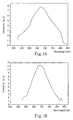
- "Poly silicon wet etching”has the same shortcomings as dry etching described above. Referring to Fig. 1, the results of the substrate surface treated with “poly silicon dry etching” and “poly silicon wet etching” separately are shown.
- Fig. 1Ashows the absorption of the poly silicon substrate surface after dry etching, and Fig.
- Another method for treating the substrateis "wet etching" the surface of the silicon wafer directly. Nevertheless, the etched surface is not adequately smooth because the etching state is difficult to control.
- An electrochemical methodis also used to form anti-reflective layers directly on substrates.
- a biasis applied under the wafer, and a direction is provided whereby the wafer is etched.
- the methodincurs the same defects as the wet etching method does, i.e., it is very difficult to control the etching state, and only a nearly smooth surface is eventually obtained.
- the conventional methods described abovesuffer from the difficulty to control the etching state, and thus increase the complexity of the process. Further, the devices produced from the conventional method above can be operated within a narrow range of wavelength, that means the reflective efficiency of the devices is high, and the energy transferring efficiency is low because most light is reflected from the device. Hence, a reflective layer having a high absorption within a broad range of wavelength is beneficial to keep light inside the device. Thus, there is an urgent need for a reflective layer with high absorption, and the method for making the reflective layer to be developed.
- the object of the present inventionis to provide an anti-reflective substrate, and the manufacturing method of the substrate.
- the methodcomprises the steps of: (a) providing a substrate; (b) depositing an amorphous silicon layer on the substrate; and (c) etching the amorphous silicon layer and the substrate by chemical etching in solutions, and the amorphous silicon layer is removed by the solutions.
- the substrate utilized in step (a) of the present inventioncan be any substrate used in the conventional method, but preferably is a silicon wafer, a glass substrate, a metal substrate, or a plastic substrate.
- the amorphous silicon layercan be deposited thoroughly on the substrate of a silicon wafer hence, the most preferable substrate utilized in step (a) of the present invention is a silicon wafer.
- the suitable deposition method of the present inventionis not limited.
- PVDphysical vapor deposition
- CVDchemical vapor deposition
- the thickness of the amorphous silicon layer deposited on the substrate in step (b)is not limited, but preferably is in a thickness of 0.5 ⁇ m-5 ⁇ m.
- the chemical etching solutions in step (c) of the present inventionare used to etch the amorphous silicon layer.
- the surface of the substrateis also etched because of the amorphous silicon layer on the substrate is formed as a sacrificial layer, and the amorphous silicon layer is finally removed completely.
- the solutions used in etchingcan be any chemical solutions or mixtures in the conventional method.
- the solutionsare hydrofluoric acid, sulfuric acid, nitric acid, phosphoric acid, or the mixture thereof.
- the etching process of the present inventioncan be any conventional one, but preferably is a wet etching process.
- the reflectance of the anti-reflective substrate produced from the method of the present inventioncan be lower than 1%, and the absorption rate of the anti-reflective substrate is preferably from 70% to 90% in a wavelength range of 300nm-900nm; and more preferably, the absorption rate is greater than 80% in a wavelength range of 400nm-800nm.
- the present inventiondiscloses a simple method to manufacture an anti-reflective substrate, and the light reflectance is lower than any anti-reflective substrates, or anti-reflective layers produced from conventional methods. This infers that the energy transferring efficiency of the present anti-reflective substrates is higher than conventional anti-reflective substrates.
- a manufacturing method of an anti-reflective silicon waferis explained as an embodiment.
- a 1 ⁇ m-thick amorphous silicon thin filmis deposited on the surface of silicon wafer by using physical vapor deposition (PVD) process under 70°C-90°C.
- PVDphysical vapor deposition
- the amorphous silicon thin filmis to be a sacrificed layer in subsequent steps.
- the substrateis rinsed in DI water and dried with nitrogen gas, whereafter excess mist is removed by baking, and an anti-reflective substrate is obtained.
- a conventional poly silicon substrate with porous structureis provided as a comparison example.
- An amorphous silicon thin filmis deposited on the surface of silicon wafer. After annealing, re-crystallization, a poly silicon thin film is thus formed. Subsequently, the same procedure as described above is followed to prepare a conventional poly silicon substrate with porous structure as a comparison.
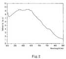
- Fig. 2shows the absorption of amorphous silicon substrate with porous structure produced from the procedure described above.
- a scanning electron microscope (SEM)is used to realize the surface morphology of the etched wafer.
- the theory of SEMis to generate electron beams by an electron gun, wherein the electron beams are then gathered into small beam size by an optoelectronic system composed of electromagnetic lenses.
- the electron beams(electron probe) irradiate onto the surface of the sample.
- the signals created from the irradiated surfaceare collected and amplified, and the amplified signals are input into a cathode ray tube which scans the surface simultaneously to display the image of the sample surface.
- Fig. 3(a)represents the morphology of a conventional poly silicon substrate with porous structure in a 1,0000X ratio
- Fig. 3(b)shows the morphology of the amorphous silicon substrate with porous structure in a 10,000X ratio. The results show that after depositing an amorphous silicon thin layer on the substrate, a highly disordered surface can be obtained by the etching process.
- the surface morphologies of both the amorphous silicon with porous structure and poly silicon substrates with porous structure produced from example 1are detected by atomic force microscopy (AFM).
- AFMis often used in surface morphology detection.
- the working theory of AFMis to detect the interactions of the near-field electromagnetic distribution or the atomic force between a micro probe and the sample surface by the micro probe.
- the surface morphology of the sampleis scanned and detected by the micro probe utilizing a tri-axial displacement piezoelectric ceramic scanner.
- Fig. 4(a)represents the morphology of a conventional poly silicon substrate with porous structure
- Fig. 4(b)shows the morphology of the amorphous silicon substrate with porous structure.
- the etched disordered surface of the amorphous silicon substrate with porous structureis more thorough than that of conventional poly silicon substrate with porous structure.
- the thoroughly disordered surfaceis advantageous for the refraction and the scattering of incident light, thus increasing the anti-reflection effect.
- Figs.5 and 6show the spectra of reflectance. Different materials of anti-reflective substrates are provided as comparison examples to the amorphous silicon substrate with porous structure in example 1.
- Fig. 5represents the reflectance of both the conventional poly silicon substrate with porous structure and the amorphous silicon substrate with porous structure.
- the dataindicates that the reflectance of conventional poly silicon substrate with porous structure is around 10% in the wavelength range of 300-800 nm (curve A), and the reflection effect is very unstable.
- the reflectance of anti-reflective porous amorphous silicon substrate produced by the present methodis kept stable at under 1% at the wavelength range of 300-800nm (curve B).
- Fig.6illustrates the reflectance results of substrates having different anti-reflection layers of: a silicon oxide layer deposited by plasma enhanced chemical vapor deposition (PECVD) (curve C), a silicon nitride layer deposited by PECVD (curve E), a silicon oxide layer deposited by sputtering (curve F), silicon oxide layer deposited by thermo-growth (curve D), and the conventional poly silicon substrate with porous structure prepared as described in example 1 (curve A).
- PECVDplasma enhanced chemical vapor deposition
- Curve Esilicon nitride layer deposited by PECVD
- Curve Fsilicon oxide layer deposited by sputtering
- curve Dsilicon oxide layer deposited by thermo-growth
- the conventional poly silicon substrate with porous structure prepared as described in example 1curve A
- amorphous silicon substrate with porous structure (curve B) produced by the present methodhas the reflectance lower than 1% among all the substrates at the wavelength range of 300-900nm. This further confirms that the anti-re
- the anti-reflection effect of the substrates produced from example 1is evaluated by external quantum efficiency.
- the substrates prepared by wet etching wafer and conventional poly silicon substrate with porous structureare detected as well as the amorphous silicon substrate with porous structure produced by the present method.
- the external quantum efficiency of the present amorphous silicon substrate with porous structureis higher than 90% at the wavelength range of 300-900nm.
- the external quantum efficiency of the substrates prepared by wet etching wafer (curve G) and the conventional poly silicon substrate with porous structure (curve A)are both less than 90% at the same wavelength range of 300-900nm. This data obviously shows the advantages of the amorphous silicon substrate with porous structure.
Landscapes
- Physics & Mathematics (AREA)
- Chemical & Material Sciences (AREA)
- Inorganic Chemistry (AREA)
- General Physics & Mathematics (AREA)
- Optics & Photonics (AREA)
- Weting (AREA)
- Surface Treatment Of Optical Elements (AREA)
- Photovoltaic Devices (AREA)
- Laminated Bodies (AREA)
- Physical Vapour Deposition (AREA)
- Optical Elements Other Than Lenses (AREA)
Abstract
Description
- The present invention relates to an anti-reflective substrate and, more particularly, to an anti-reflective substrate with highly rugged surface and the method of manufacturing the same.
- Currently, the energy source of an optoelectronic device is from electrons transferred by photo-electric conversion. The less the light reflective ratio of the device is (more light is absorbed by the surface of the device), the higher the intensity can be obtained. Therefore, the investigation of methods for producing anti-reflective layers of optoelectronic devices with high anti-reflective efficiency is very important.
- Among the conventional methods to receive more light, one is to enhance the transmittance of incidental light by forming an anti-reflective membrane on the surface of optoelectronic devices, and another one is to etch the substrate to increase the surface area by etched porous.
- There are several methods for etching the surface of the substrate. "Poly silicon dry etching" is to form a poly silicon layer on the silicon wafer first, and etch by high density plasma etching system. However, the system is very rarely used because of high cost, and additional preparation steps of the poly silicon material are required. Therefore, the shortcomings of high cost and complex process limit the use of the method. "Poly silicon wet etching" has the same shortcomings as dry etching described above. Referring to Fig. 1, the results of the substrate surface treated with "poly silicon dry etching" and "poly silicon wet etching" separately are shown. Fig. 1A shows the absorption of the poly silicon substrate surface after dry etching, and Fig. 1B shows that from poly silicon substrate surface after wet etching. Both of the two results only show a better absorption at wavelength of 700nm. This indicates that the two methods are not able to absorb the light within a broad wavelength range, and this might also be a shortcoming of these conventional methods.
- Another method for treating the substrate is "wet etching" the surface of the silicon wafer directly. Nevertheless, the etched surface is not adequately smooth because the etching state is difficult to control.
- An electrochemical method is also used to form anti-reflective layers directly on substrates. In the electrochemical method, a bias is applied under the wafer, and a direction is provided whereby the wafer is etched. However, the method incurs the same defects as the wet etching method does, i.e., it is very difficult to control the etching state, and only a nearly smooth surface is eventually obtained.
- The conventional methods described above suffer from the difficulty to control the etching state, and thus increase the complexity of the process. Further, the devices produced from the conventional method above can be operated within a narrow range of wavelength, that means the reflective efficiency of the devices is high, and the energy transferring efficiency is low because most light is reflected from the device. Hence, a reflective layer having a high absorption within a broad range of wavelength is beneficial to keep light inside the device. Thus, there is an urgent need for a reflective layer with high absorption, and the method for making the reflective layer to be developed.
- The object of the present invention is to provide an anti-reflective substrate, and the manufacturing method of the substrate. The method comprises the steps of: (a) providing a substrate; (b) depositing an amorphous silicon layer on the substrate; and (c) etching the amorphous silicon layer and the substrate by chemical etching in solutions, and the amorphous silicon layer is removed by the solutions.
- The substrate utilized in step (a) of the present invention can be any substrate used in the conventional method, but preferably is a silicon wafer, a glass substrate, a metal substrate, or a plastic substrate. The amorphous silicon layer can be deposited thoroughly on the substrate of a silicon wafer hence, the most preferable substrate utilized in step (a) of the present invention is a silicon wafer.
- To deposit the amorphous silicon layer on the substrate, the suitable deposition method of the present invention is not limited. Preferably, physical vapor deposition (PVD) or chemical vapor deposition (CVD) can be performed in step (b). The thickness of the amorphous silicon layer deposited on the substrate in step (b) is not limited, but preferably is in a thickness of 0.5µm-5µm.
- The chemical etching solutions in step (c) of the present invention are used to etch the amorphous silicon layer. The surface of the substrate is also etched because of the amorphous silicon layer on the substrate is formed as a sacrificial layer, and the amorphous silicon layer is finally removed completely. The solutions used in etching can be any chemical solutions or mixtures in the conventional method. Preferably, the solutions are hydrofluoric acid, sulfuric acid, nitric acid, phosphoric acid, or the mixture thereof. Furthermore, the etching process of the present invention can be any conventional one, but preferably is a wet etching process.
- The reflectance of the anti-reflective substrate produced from the method of the present invention can be lower than 1%, and the absorption rate of the anti-reflective substrate is preferably from 70% to 90% in a wavelength range of 300nm-900nm; and more preferably, the absorption rate is greater than 80% in a wavelength range of 400nm-800nm.
- The present invention discloses a simple method to manufacture an anti-reflective substrate, and the light reflectance is lower than any anti-reflective substrates, or anti-reflective layers produced from conventional methods. This infers that the energy transferring efficiency of the present anti-reflective substrates is higher than conventional anti-reflective substrates.
- Other objects, advantages, and novel features of the invention will become more apparent from the following detailed description when taken in conjunction with the accompanying drawings.
- Fig. 1A shows the absorption of the poly silicon substrate after dry etching;
- Fig. 1B shows the absorption of the poly silicon substrate surface wet etching;
- Fig. 2 shows the absorption of amorphous silicon substrate with porous structure produced by the present invention in example 1;
- Fig. 3 represents the data observed by SEM in example 2, Fig.3 (a) is the morphology of a conventional poly silicon substrate with porous structure in 1,0000X ratio, and Fig. 3(b) shows the morphology of the amorphous silicon substrate with porous structure in a 10,000X ratio;
- Fig. 4 represents the surface morphology of example 3 by AFM, Fig. 4(a) represents the surface morphology of a conventional poly silicon substrate with porous structure, and Fig. 4(b) shows the surface morphology of the present invention;
- Fig. 5 represents the reflectance of both conventional poly silicon substrate with porous structure (curve A) and the amorphous silicon substrate with porous structure (curve B) in example 4;
- Fig. 6 illustrates the reflectance results of substrates having different anti-reflection layers in example 4; and
- Fig. 7 shows the external quantum efficiency of the conventional poly silicon substrate with structure (curve A), the amorphous silicon substrate with porous structure (curve B), and the wet-etched (curve G).
- A manufacturing method of an anti-reflective silicon wafer is explained as an embodiment. First, a 1 µm-thick amorphous silicon thin film is deposited on the surface of silicon wafer by using physical vapor deposition (PVD) process under 70°C-90°C. The amorphous silicon thin film is to be a sacrificed layer in subsequent steps. The surface of the substrate is etched to become a porous textured structure in the etching solution (HF: HNO3=100:1). Ultrasonic vibration is also performed while etching to ensure uniform etching and thus keeps the surface of the substrate in a highly rugged condition.
- After etching, the substrate is rinsed in DI water and dried with nitrogen gas, whereafter excess mist is removed by baking, and an anti-reflective substrate is obtained.
- In addition, a conventional poly silicon substrate with porous structure is provided as a comparison example. An amorphous silicon thin film is deposited on the surface of silicon wafer. After annealing, re-crystallization, a poly silicon thin film is thus formed. Subsequently, the same procedure as described above is followed to prepare a conventional poly silicon substrate with porous structure as a comparison.
- Fig. 2 shows the absorption of amorphous silicon substrate with porous structure produced from the procedure described above.
- A scanning electron microscope (SEM) is used to realize the surface morphology of the etched wafer.
- The theory of SEM is to generate electron beams by an electron gun, wherein the electron beams are then gathered into small beam size by an optoelectronic system composed of electromagnetic lenses. The electron beams (electron probe) irradiate onto the surface of the sample. The signals created from the irradiated surface are collected and amplified, and the amplified signals are input into a cathode ray tube which scans the surface simultaneously to display the image of the sample surface.
- The surface morphologies of both the amorphous silicon substrate with porous structure and conventional poly silicon substrates with porous structure produced from example 1 are detected by SEM, and the results are shown in Fig. 3. Fig. 3(a) represents the morphology of a conventional poly silicon substrate with porous structure in a 1,0000X ratio, and Fig. 3(b) shows the morphology of the amorphous silicon substrate with porous structure in a 10,000X ratio. The results show that after depositing an amorphous silicon thin layer on the substrate, a highly disordered surface can be obtained by the etching process.
- The surface morphologies of both the amorphous silicon with porous structure and poly silicon substrates with porous structure produced from example 1 are detected by atomic force microscopy (AFM). The AFM is often used in surface morphology detection. The working theory of AFM is to detect the interactions of the near-field electromagnetic distribution or the atomic force between a micro probe and the sample surface by the micro probe. The surface morphology of the sample is scanned and detected by the micro probe utilizing a tri-axial displacement piezoelectric ceramic scanner.
- The results are shown in Fig. 4. Fig. 4(a) represents the morphology of a conventional poly silicon substrate with porous structure, and Fig. 4(b) shows the morphology of the amorphous silicon substrate with porous structure. According to the data, the etched disordered surface of the amorphous silicon substrate with porous structure is more thorough than that of conventional poly silicon substrate with porous structure. The thoroughly disordered surface is advantageous for the refraction and the scattering of incident light, thus increasing the anti-reflection effect.
- The anti-reflection effect of the substrates produced from example 1 is evaluated by use of a fluorescence spectrometer. Figs.5 and 6 show the spectra of reflectance. Different materials of anti-reflective substrates are provided as comparison examples to the amorphous silicon substrate with porous structure in example 1. Fig. 5 represents the reflectance of both the conventional poly silicon substrate with porous structure and the amorphous silicon substrate with porous structure. The data indicates that the reflectance of conventional poly silicon substrate with porous structure is around 10% in the wavelength range of 300-800 nm (curve A), and the reflection effect is very unstable. However, the reflectance of anti-reflective porous amorphous silicon substrate produced by the present method is kept stable at under 1% at the wavelength range of 300-800nm (curve B).
- Fig.6 illustrates the reflectance results of substrates having different anti-reflection layers of: a silicon oxide layer deposited by plasma enhanced chemical vapor deposition (PECVD) (curve C), a silicon nitride layer deposited by PECVD (curve E), a silicon oxide layer deposited by sputtering (curve F), silicon oxide layer deposited by thermo-growth (curve D), and the conventional poly silicon substrate with porous structure prepared as described in example 1 (curve A). According to Fig. 6, only the amorphous silicon substrate with porous structure (curve B) produced by the present method has the reflectance lower than 1% among all the substrates at the wavelength range of 300-900nm. This further confirms that the anti-reflective substrate produced by the present method has a high absorption to light.
- The anti-reflection effect of the substrates produced from example 1 is evaluated by external quantum efficiency. The substrates prepared by wet etching wafer and conventional poly silicon substrate with porous structure are detected as well as the amorphous silicon substrate with porous structure produced by the present method.
- According to the result shown in Fig. 7, the external quantum efficiency of the present amorphous silicon substrate with porous structure (curve B) is higher than 90% at the wavelength range of 300-900nm. However, the external quantum efficiency of the substrates prepared by wet etching wafer (curve G) and the conventional poly silicon substrate with porous structure (curve A) are both less than 90% at the same wavelength range of 300-900nm. This data obviously shows the advantages of the amorphous silicon substrate with porous structure.
- Although the present invention has been explained in relation to its preferred embodiment, it is to be understood that many other possible modifications and variations can be made without departing from the spirit and scope of the invention as hereinafter claimed.
Claims (18)
- A method for producing an anti-reflective substrate, comprising the steps of:(a) providing a substrate;(b) depositing an amorphous silicon layer on the substrate; and(c) etching the amorphous silicon layer and the substrate by chemical etching in solutions, and the amorphous silicon layer is removed by the solutions.
- The method as claimed in claim 1, wherein the substrate utilized in step (a) is a silicon wafer, a glass substrate, a metal substrate, or a plastic substrate.
- The method as claimed in claim 1, wherein the substrate utilized in step (a) is a silicon wafer.
- The method as claimed in claim 1, wherein physical vapor deposition (PVD) or chemical vapor deposition (CVD) is performed in step (b).
- The method as claimed in claim 1, wherein the amorphous silicon layer deposited in step (b) is in a thickness of 0.5µm-5µm.
- The method as claimed in claim 1, wherein the chemical etching solutions in step (c) are hydrofluoric acid, sulfuric acid, nitric acid, phosphoric acid, or the mixture thereof.
- The method as claimed in claim 1, wherein the effective reflectance of the anti-reflective substrate produced thereby is lower than 1%.
- The method as claimed in claim 1, wherein the absorption of the anti-reflective substrate produced thereby is from 70% to 90% in a wavelength range of 300nm-900nm.
- The method as claimed in claim 1, wherein the absorption of the anti-reflective substrate produced thereby is greater than 80% in a wavelength range of 400nm-800nm.
- An anti-reflective substrate produced by a method comprising the steps of:(a) providing a substrate;(b) depositing an amorphous silicon layer on the substrate; and(c) etching the amorphous silicon layer and the substrate by chemical etching in solutions, and the amorphous silicon layer is removed by the solutions.
- The substrate as claimed in claim 10, wherein the substrate utilized in step (a) is a silicon wafer, a glass substrate, a metal substrate, or a plastic substrate.
- The substrate as claimed in claim 10, wherein the substrate utilized in step (a) is a silicon wafer.
- The substrate as claimed in claim 10, wherein physical vapor deposition (PVD) or chemical vapor deposition (CVD) is performed in step (b).
- The substrate as claimed in claim 10, wherein the amorphous silicon layer deposited in step (b) is in a thickness of 0.5µm-5µm.
- The substrate as claimed in claim 10, wherein the chemical etching solutions in step (c) are hydrofluoric acid, sulfuric acid, nitric acid, phosphoric acid, or the mixture thereof.
- The substrate as claimed in claim 10, wherein the effective reflectance of the anti-reflective substrate is lower than 1%.
- The substrate as claimed in claim 10, wherein the absorption of the anti-reflective substrate is from 70% to 90% in a wavelength range of 300nm-900nm.
- The substrate as claimed in claim 10, wherein the absorption of the anti-reflective substrate is greater than 80% in a wavelength range of 400nm-800nm.
Applications Claiming Priority (1)
| Application Number | Priority Date | Filing Date | Title |
|---|---|---|---|
| TW094139436ATWI267897B (en) | 2005-11-10 | 2005-11-10 | Substrate with anti-reflection layer and its manufacturing method |
Publications (2)
| Publication Number | Publication Date |
|---|---|
| EP1845562A1true EP1845562A1 (en) | 2007-10-17 |
| EP1845562B1 EP1845562B1 (en) | 2011-06-08 |
Family
ID=38004271
Family Applications (1)
| Application Number | Title | Priority Date | Filing Date |
|---|---|---|---|
| EP06252031ANot-in-forceEP1845562B1 (en) | 2005-11-10 | 2006-04-12 | Manufacturing method for an anti-reflective substrate |
Country Status (7)
| Country | Link |
|---|---|
| US (1) | US7524773B2 (en) |
| EP (1) | EP1845562B1 (en) |
| JP (1) | JP4560652B2 (en) |
| AU (1) | AU2006201341B2 (en) |
| CA (1) | CA2541879C (en) |
| ES (1) | ES2366480T3 (en) |
| TW (1) | TWI267897B (en) |
Families Citing this family (4)
| Publication number | Priority date | Publication date | Assignee | Title |
|---|---|---|---|---|
| KR20120135185A (en)* | 2009-09-21 | 2012-12-12 | 바스프 에스이 | Acqueous acidic etching solution and method for texturing the surface of single crystal and polycrystal silicon substrates |
| JP2013012705A (en)* | 2011-06-01 | 2013-01-17 | Sumco Corp | Wafer for solar cell, solar cell and solar cell module |
| JP5912538B2 (en)* | 2012-01-10 | 2016-04-27 | 株式会社半導体エネルギー研究所 | Semiconductor substrate and photoelectric conversion device made of silicon |
| US20140161990A1 (en)* | 2012-12-12 | 2014-06-12 | Intermolecular, Inc. | Anti-Glare Glass/Substrate Via Novel Specific Combinations of Dry and Wet Processes |
Citations (7)
| Publication number | Priority date | Publication date | Assignee | Title |
|---|---|---|---|---|
| US4137123A (en)* | 1975-12-31 | 1979-01-30 | Motorola, Inc. | Texture etching of silicon: method |
| US4252865A (en)* | 1978-05-24 | 1981-02-24 | National Patent Development Corporation | Highly solar-energy absorbing device and method of making the same |
| US4348254A (en)* | 1978-12-27 | 1982-09-07 | Solarex Corporation | Method of making solar cell |
| EP0724299A2 (en)* | 1995-01-27 | 1996-07-31 | AT&T Corp. | Article comprising a Si-based photodetector |
| US20020119290A1 (en)* | 2001-01-03 | 2002-08-29 | Sang-Wook Park | Textured semiconductor wafer for solar cell |
| US20030181014A1 (en)* | 2002-03-19 | 2003-09-25 | Fujitsu Limited | Method of manufacturing semiconductor device with STI |
| US20050104163A1 (en)* | 2001-11-29 | 2005-05-19 | Weber Klaus J. | Semiconductor texturing process |
Family Cites Families (15)
| Publication number | Priority date | Publication date | Assignee | Title |
|---|---|---|---|---|
| US4285762A (en)* | 1979-12-31 | 1981-08-25 | Exxon Research & Engineering Co. | Plasma etching of amorphous silicon (SE-35) |
| GB2170649A (en)* | 1985-01-18 | 1986-08-06 | Intel Corp | Sputtered silicon as an anti-reflective coating for metal layer lithography |
| US5641708A (en)* | 1994-06-07 | 1997-06-24 | Sgs-Thomson Microelectronics, Inc. | Method for fabricating conductive structures in integrated circuits |
| US5854132A (en)* | 1994-11-29 | 1998-12-29 | Advanced Micro Devices, Inc. | Method for exposing photoresist |
| US5986311A (en)* | 1997-05-19 | 1999-11-16 | Citizen Watch Company, Ltd. | Semiconductor device having recrystallized source/drain regions |
| JP2000261008A (en)* | 1999-03-10 | 2000-09-22 | Mitsubishi Electric Corp | Surface roughening method for silicon substrate for solar cell |
| US6204117B1 (en)* | 1999-07-14 | 2001-03-20 | United Microelectronics Corp. | Removal of silicon oxynitride on a capacitor electrode for selective hemispherical grain growth |
| US6586339B1 (en)* | 1999-10-28 | 2003-07-01 | Advanced Micro Devices, Inc. | Silicon barrier layer to prevent resist poisoning |
| JP2003309276A (en)* | 2002-04-16 | 2003-10-31 | Sharp Corp | Substrate surface processing method and solar cell |
| JP4049329B2 (en)* | 2002-06-06 | 2008-02-20 | 関西ティー・エル・オー株式会社 | Method for producing polycrystalline silicon substrate for solar cell |
| JP2004103736A (en)* | 2002-09-06 | 2004-04-02 | Ebara Corp | Solar cell manufacturing method |
| JP2004281758A (en)* | 2003-03-17 | 2004-10-07 | Sharp Corp | Solar cell and method of manufacturing the same |
| AU2003901559A0 (en)* | 2003-04-07 | 2003-05-01 | Unisearch Limited | Glass texturing method |
| JP3925867B2 (en)* | 2003-12-17 | 2007-06-06 | 関西ティー・エル・オー株式会社 | Method for manufacturing a silicon substrate with a porous layer |
| JP2005303255A (en)* | 2004-03-17 | 2005-10-27 | Shinryo Corp | Low reflectance processing method for solar cell silicon substrate |
- 2005
- 2005-11-10TWTW094139436Apatent/TWI267897B/ennot_activeIP Right Cessation
- 2006
- 2006-03-28USUS11/390,223patent/US7524773B2/enactiveActive
- 2006-03-30AUAU2006201341Apatent/AU2006201341B2/ennot_activeCeased
- 2006-04-03CACA002541879Apatent/CA2541879C/enactiveActive
- 2006-04-12EPEP06252031Apatent/EP1845562B1/ennot_activeNot-in-force
- 2006-04-12ESES06252031Tpatent/ES2366480T3/enactiveActive
- 2006-04-28JPJP2006124777Apatent/JP4560652B2/ennot_activeExpired - Fee Related
Patent Citations (7)
| Publication number | Priority date | Publication date | Assignee | Title |
|---|---|---|---|---|
| US4137123A (en)* | 1975-12-31 | 1979-01-30 | Motorola, Inc. | Texture etching of silicon: method |
| US4252865A (en)* | 1978-05-24 | 1981-02-24 | National Patent Development Corporation | Highly solar-energy absorbing device and method of making the same |
| US4348254A (en)* | 1978-12-27 | 1982-09-07 | Solarex Corporation | Method of making solar cell |
| EP0724299A2 (en)* | 1995-01-27 | 1996-07-31 | AT&T Corp. | Article comprising a Si-based photodetector |
| US20020119290A1 (en)* | 2001-01-03 | 2002-08-29 | Sang-Wook Park | Textured semiconductor wafer for solar cell |
| US20050104163A1 (en)* | 2001-11-29 | 2005-05-19 | Weber Klaus J. | Semiconductor texturing process |
| US20030181014A1 (en)* | 2002-03-19 | 2003-09-25 | Fujitsu Limited | Method of manufacturing semiconductor device with STI |
Also Published As
| Publication number | Publication date |
|---|---|
| US7524773B2 (en) | 2009-04-28 |
| JP4560652B2 (en) | 2010-10-13 |
| AU2006201341A1 (en) | 2007-05-24 |
| AU2006201341B2 (en) | 2007-10-18 |
| US20070105266A1 (en) | 2007-05-10 |
| JP2007134667A (en) | 2007-05-31 |
| CA2541879C (en) | 2009-07-28 |
| EP1845562B1 (en) | 2011-06-08 |
| CA2541879A1 (en) | 2007-05-10 |
| ES2366480T3 (en) | 2011-10-20 |
| TWI267897B (en) | 2006-12-01 |
| TW200719393A (en) | 2007-05-16 |
Similar Documents
| Publication | Publication Date | Title |
|---|---|---|
| Zijlstra et al. | Fabrication of two-dimensional photonic crystal waveguides for 1.5 μm in silicon by deep anisotropic dry etching | |
| JP3855105B2 (en) | Method for creating a roughened surface on a silicon solar cell substrate | |
| US6533907B2 (en) | Method of producing amorphous silicon for hard mask and waveguide applications | |
| Zeng et al. | Preparation of composite micro/nano structure on the silicon surface by reactive ion etching: Enhanced anti-reflective and hydrophobic properties | |
| JP6617300B2 (en) | Method for randomly texturing a semiconductor substrate | |
| EP1845562B1 (en) | Manufacturing method for an anti-reflective substrate | |
| JP2017518646A5 (en) | ||
| US20230261124A1 (en) | High absorption photovoltaic material and methods of making the same | |
| Shin et al. | A highly ordered and damage-free Ge inverted pyramid array structure for broadband antireflection in the mid-infrared | |
| Zhang et al. | Facile and stable fabrication of wafer-scale, ultra-black c-silicon with 3D nano/micro hybrid structures for solar cells | |
| KR20100097369A (en) | Method for manufacturing lithography-free fabrication of subwavelength antireflection structures using thermally dewetted alloy etch mask and substrate manufactured with said method | |
| Grover et al. | Process development of methane–hydrogen–argon-based deep dry etching of InP for high aspect-ratio structures with vertical facet-quality sidewalls | |
| KR101731497B1 (en) | Method for texturing of semiconductor substrate, semiconductor substrate manufactured by the method and solar cell comprising the same | |
| CN112612078A (en) | High-efficiency coupling waveguide based on GOI or SOI and preparation method thereof | |
| Zhang et al. | Morphology evolution of the light trapping structure using atmospheric plasma textured c-Si wafer for silicon solar cells | |
| CN1971950B (en) | Anti-reflection layer substrate and manufacturing method thereof | |
| Liu et al. | Moth-eye antireflection nanostructure on glass for CubeSats | |
| CN100365780C (en) | Mask layer and preparation method for reactive ion etching mercury cadmium telluride micro-mesas array | |
| Stoltz et al. | Antireflective structures in CDTE and CDZNTE surfaces by ECR plasma etching | |
| US20090221144A1 (en) | Manufacturing method for nano scale Ge metal structure | |
| Chu et al. | Room-temperature radio frequency sputtered Ta 2 O 5: A new etch mask for bulk silicon dissolved processes | |
| TW201328965A (en) | Method of fabricating anti-reflective layer and anti-reflective layer fabricated by the same | |
| Kashyap et al. | Absorption enhancement by surface texturing in ZnO/Si heterojunction | |
| KR100349929B1 (en) | fabrication method of a nanosize metal aperture tip for NOSM sensor | |
| Eisenhauer et al. | Improved light management in crystalline silicon thin-film solar cells by advanced nano-texture fabrication |
Legal Events
| Date | Code | Title | Description |
|---|---|---|---|
| PUAI | Public reference made under article 153(3) epc to a published international application that has entered the european phase | Free format text:ORIGINAL CODE: 0009012 | |
| AK | Designated contracting states | Kind code of ref document:A1 Designated state(s):AT BE BG CH CY CZ DE DK EE ES FI FR GB GR HU IE IS IT LI LT LU LV MC NL PL PT RO SE SI SK TR | |
| AX | Request for extension of the european patent | Extension state:AL BA HR MK YU | |
| 17P | Request for examination filed | Effective date:20080315 | |
| 17Q | First examination report despatched | Effective date:20080415 | |
| AKX | Designation fees paid | Designated state(s):DE ES NL | |
| GRAP | Despatch of communication of intention to grant a patent | Free format text:ORIGINAL CODE: EPIDOSNIGR1 | |
| RIC1 | Information provided on ipc code assigned before grant | Ipc:G02B 1/11 20060101ALI20100719BHEP Ipc:H01L 31/0236 20060101AFI20100719BHEP | |
| RTI1 | Title (correction) | Free format text:MANUFACTURING METHOD FOR AN ANTI-REFLECTIVE SUBSTRATE | |
| GRAS | Grant fee paid | Free format text:ORIGINAL CODE: EPIDOSNIGR3 | |
| RAP1 | Party data changed (applicant data changed or rights of an application transferred) | Owner name:TATUNG UNIVERSITY Owner name:TATUNG COMPANY | |
| GRAA | (expected) grant | Free format text:ORIGINAL CODE: 0009210 | |
| AK | Designated contracting states | Kind code of ref document:B1 Designated state(s):DE ES NL | |
| REG | Reference to a national code | Ref country code:DE Ref legal event code:R096 Ref document number:602006022359 Country of ref document:DE Effective date:20110721 | |
| REG | Reference to a national code | Ref country code:NL Ref legal event code:T3 | |
| REG | Reference to a national code | Ref country code:ES Ref legal event code:FG2A Ref document number:2366480 Country of ref document:ES Kind code of ref document:T3 Effective date:20111020 | |
| PLBE | No opposition filed within time limit | Free format text:ORIGINAL CODE: 0009261 | |
| STAA | Information on the status of an ep patent application or granted ep patent | Free format text:STATUS: NO OPPOSITION FILED WITHIN TIME LIMIT | |
| 26N | No opposition filed | Effective date:20120309 | |
| REG | Reference to a national code | Ref country code:DE Ref legal event code:R097 Ref document number:602006022359 Country of ref document:DE Effective date:20120309 | |
| PGFP | Annual fee paid to national office [announced via postgrant information from national office to epo] | Ref country code:NL Payment date:20230424 Year of fee payment:18 | |
| PGFP | Annual fee paid to national office [announced via postgrant information from national office to epo] | Ref country code:ES Payment date:20230505 Year of fee payment:18 Ref country code:DE Payment date:20220624 Year of fee payment:18 | |
| REG | Reference to a national code | Ref country code:DE Ref legal event code:R119 Ref document number:602006022359 Country of ref document:DE | |
| REG | Reference to a national code | Ref country code:DE Ref legal event code:R079 Ref document number:602006022359 Country of ref document:DE Free format text:PREVIOUS MAIN CLASS: H01L0031023600 Ipc:H10F0077700000 | |
| REG | Reference to a national code | Ref country code:NL Ref legal event code:MM Effective date:20240501 | |
| PG25 | Lapsed in a contracting state [announced via postgrant information from national office to epo] | Ref country code:DE Free format text:LAPSE BECAUSE OF NON-PAYMENT OF DUE FEES Effective date:20241105 | |
| PG25 | Lapsed in a contracting state [announced via postgrant information from national office to epo] | Ref country code:NL Free format text:LAPSE BECAUSE OF NON-PAYMENT OF DUE FEES Effective date:20240501 | |
| PG25 | Lapsed in a contracting state [announced via postgrant information from national office to epo] | Ref country code:NL Free format text:LAPSE BECAUSE OF NON-PAYMENT OF DUE FEES Effective date:20240501 Ref country code:DE Free format text:LAPSE BECAUSE OF NON-PAYMENT OF DUE FEES Effective date:20241105 | |
| REG | Reference to a national code | Ref country code:ES Ref legal event code:FD2A Effective date:20250528 | |
| PG25 | Lapsed in a contracting state [announced via postgrant information from national office to epo] | Ref country code:ES Free format text:LAPSE BECAUSE OF NON-PAYMENT OF DUE FEES Effective date:20240413 |