EP1831970B1 - Midplane especially applicable to an orthogonal architecture electronic system - Google Patents
Midplane especially applicable to an orthogonal architecture electronic systemDownload PDFInfo
- Publication number
- EP1831970B1 EP1831970B1EP05855654.9AEP05855654AEP1831970B1EP 1831970 B1EP1831970 B1EP 1831970B1EP 05855654 AEP05855654 AEP 05855654AEP 1831970 B1EP1831970 B1EP 1831970B1
- Authority
- EP
- European Patent Office
- Prior art keywords
- signal
- launches
- pair
- connector
- vias
- Prior art date
- Legal status (The legal status is an assumption and is not a legal conclusion. Google has not performed a legal analysis and makes no representation as to the accuracy of the status listed.)
- Not-in-force
Links
- 239000004020conductorSubstances0.000claimsdescription174
- 230000013011matingEffects0.000claimsdescription18
- 235000012431wafersNutrition0.000description10
- 230000008878couplingEffects0.000description6
- 238000010168coupling processMethods0.000description6
- 238000005859coupling reactionMethods0.000description6
- 238000000034methodMethods0.000description4
- 230000005540biological transmissionEffects0.000description3
- 239000000463materialSubstances0.000description3
- 230000000712assemblyEffects0.000description2
- 238000000429assemblyMethods0.000description2
- 238000006243chemical reactionMethods0.000description2
- 230000007423decreaseEffects0.000description2
- 238000010586diagramMethods0.000description2
- 230000005288electromagnetic effectEffects0.000description2
- 229910000679solderInorganic materials0.000description2
- 238000005476solderingMethods0.000description2
- 239000000758substrateSubstances0.000description2
- 238000004891communicationMethods0.000description1
- 238000010276constructionMethods0.000description1
- 230000003247decreasing effectEffects0.000description1
- 230000000593degrading effectEffects0.000description1
- 238000006073displacement reactionMethods0.000description1
- 230000000694effectsEffects0.000description1
- 230000005672electromagnetic fieldEffects0.000description1
- 238000004519manufacturing processMethods0.000description1
- 230000007246mechanismEffects0.000description1
- 239000002184metalSubstances0.000description1
- 230000001902propagating effectEffects0.000description1
- 230000005855radiationEffects0.000description1
- 230000007704transitionEffects0.000description1
Images


Classifications
- H—ELECTRICITY
- H01—ELECTRIC ELEMENTS
- H01R—ELECTRICALLY-CONDUCTIVE CONNECTIONS; STRUCTURAL ASSOCIATIONS OF A PLURALITY OF MUTUALLY-INSULATED ELECTRICAL CONNECTING ELEMENTS; COUPLING DEVICES; CURRENT COLLECTORS
- H01R12/00—Structural associations of a plurality of mutually-insulated electrical connecting elements, specially adapted for printed circuits, e.g. printed circuit boards [PCB], flat or ribbon cables, or like generally planar structures, e.g. terminal strips, terminal blocks; Coupling devices specially adapted for printed circuits, flat or ribbon cables, or like generally planar structures; Terminals specially adapted for contact with, or insertion into, printed circuits, flat or ribbon cables, or like generally planar structures
- H—ELECTRICITY
- H01—ELECTRIC ELEMENTS
- H01R—ELECTRICALLY-CONDUCTIVE CONNECTIONS; STRUCTURAL ASSOCIATIONS OF A PLURALITY OF MUTUALLY-INSULATED ELECTRICAL CONNECTING ELEMENTS; COUPLING DEVICES; CURRENT COLLECTORS
- H01R13/00—Details of coupling devices of the kinds covered by groups H01R12/70 or H01R24/00 - H01R33/00
- H01R13/648—Protective earth or shield arrangements on coupling devices, e.g. anti-static shielding
- H01R13/658—High frequency shielding arrangements, e.g. against EMI [Electro-Magnetic Interference] or EMP [Electro-Magnetic Pulse]
- H01R13/6581—Shield structure
- H01R13/6585—Shielding material individually surrounding or interposed between mutually spaced contacts
- H01R13/6586—Shielding material individually surrounding or interposed between mutually spaced contacts for separating multiple connector modules
- H01R13/6587—Shielding material individually surrounding or interposed between mutually spaced contacts for separating multiple connector modules for mounting on PCBs
- H—ELECTRICITY
- H01—ELECTRIC ELEMENTS
- H01R—ELECTRICALLY-CONDUCTIVE CONNECTIONS; STRUCTURAL ASSOCIATIONS OF A PLURALITY OF MUTUALLY-INSULATED ELECTRICAL CONNECTING ELEMENTS; COUPLING DEVICES; CURRENT COLLECTORS
- H01R13/00—Details of coupling devices of the kinds covered by groups H01R12/70 or H01R24/00 - H01R33/00
- H01R13/648—Protective earth or shield arrangements on coupling devices, e.g. anti-static shielding
- H01R13/658—High frequency shielding arrangements, e.g. against EMI [Electro-Magnetic Interference] or EMP [Electro-Magnetic Pulse]
- H01R13/6591—Specific features or arrangements of connection of shield to conductive members
- H—ELECTRICITY
- H05—ELECTRIC TECHNIQUES NOT OTHERWISE PROVIDED FOR
- H05K—PRINTED CIRCUITS; CASINGS OR CONSTRUCTIONAL DETAILS OF ELECTRIC APPARATUS; MANUFACTURE OF ASSEMBLAGES OF ELECTRICAL COMPONENTS
- H05K1/00—Printed circuits
- H05K1/02—Details
- H05K1/11—Printed elements for providing electric connections to or between printed circuits
- H05K1/115—Via connections; Lands around holes or via connections
- H05K1/116—Lands, clearance holes or other lay-out details concerning the surrounding of a via
- H—ELECTRICITY
- H05—ELECTRIC TECHNIQUES NOT OTHERWISE PROVIDED FOR
- H05K—PRINTED CIRCUITS; CASINGS OR CONSTRUCTIONAL DETAILS OF ELECTRIC APPARATUS; MANUFACTURE OF ASSEMBLAGES OF ELECTRICAL COMPONENTS
- H05K1/00—Printed circuits
- H05K1/02—Details
- H05K1/14—Structural association of two or more printed circuits
- H—ELECTRICITY
- H05—ELECTRIC TECHNIQUES NOT OTHERWISE PROVIDED FOR
- H05K—PRINTED CIRCUITS; CASINGS OR CONSTRUCTIONAL DETAILS OF ELECTRIC APPARATUS; MANUFACTURE OF ASSEMBLAGES OF ELECTRICAL COMPONENTS
- H05K7/00—Constructional details common to different types of electric apparatus
- H05K7/14—Mounting supporting structure in casing or on frame or rack
- H05K7/1438—Back panels or connecting means therefor; Terminals; Coding means to avoid wrong insertion
- H05K7/1439—Back panel mother boards
- H05K7/1445—Back panel mother boards with double-sided connections
- H—ELECTRICITY
- H01—ELECTRIC ELEMENTS
- H01R—ELECTRICALLY-CONDUCTIVE CONNECTIONS; STRUCTURAL ASSOCIATIONS OF A PLURALITY OF MUTUALLY-INSULATED ELECTRICAL CONNECTING ELEMENTS; COUPLING DEVICES; CURRENT COLLECTORS
- H01R13/00—Details of coupling devices of the kinds covered by groups H01R12/70 or H01R24/00 - H01R33/00
- H01R13/46—Bases; Cases
- H01R13/514—Bases; Cases composed as a modular blocks or assembly, i.e. composed of co-operating parts provided with contact members or holding contact members between them
- H—ELECTRICITY
- H05—ELECTRIC TECHNIQUES NOT OTHERWISE PROVIDED FOR
- H05K—PRINTED CIRCUITS; CASINGS OR CONSTRUCTIONAL DETAILS OF ELECTRIC APPARATUS; MANUFACTURE OF ASSEMBLAGES OF ELECTRICAL COMPONENTS
- H05K1/00—Printed circuits
- H05K1/02—Details
- H05K1/0213—Electrical arrangements not otherwise provided for
- H05K1/0216—Reduction of cross-talk, noise or electromagnetic interference
- H05K1/023—Reduction of cross-talk, noise or electromagnetic interference using auxiliary mounted passive components or auxiliary substances
- H05K1/0231—Capacitors or dielectric substances
- H—ELECTRICITY
- H05—ELECTRIC TECHNIQUES NOT OTHERWISE PROVIDED FOR
- H05K—PRINTED CIRCUITS; CASINGS OR CONSTRUCTIONAL DETAILS OF ELECTRIC APPARATUS; MANUFACTURE OF ASSEMBLAGES OF ELECTRICAL COMPONENTS
- H05K1/00—Printed circuits
- H05K1/02—Details
- H05K1/0213—Electrical arrangements not otherwise provided for
- H05K1/0237—High frequency adaptations
- H—ELECTRICITY
- H05—ELECTRIC TECHNIQUES NOT OTHERWISE PROVIDED FOR
- H05K—PRINTED CIRCUITS; CASINGS OR CONSTRUCTIONAL DETAILS OF ELECTRIC APPARATUS; MANUFACTURE OF ASSEMBLAGES OF ELECTRICAL COMPONENTS
- H05K2201/00—Indexing scheme relating to printed circuits covered by H05K1/00
- H05K2201/04—Assemblies of printed circuits
- H05K2201/044—Details of backplane or midplane for mounting orthogonal PCBs
- H—ELECTRICITY
- H05—ELECTRIC TECHNIQUES NOT OTHERWISE PROVIDED FOR
- H05K—PRINTED CIRCUITS; CASINGS OR CONSTRUCTIONAL DETAILS OF ELECTRIC APPARATUS; MANUFACTURE OF ASSEMBLAGES OF ELECTRICAL COMPONENTS
- H05K2201/00—Indexing scheme relating to printed circuits covered by H05K1/00
- H05K2201/09—Shape and layout
- H05K2201/09209—Shape and layout details of conductors
- H05K2201/09218—Conductive traces
- H05K2201/09236—Parallel layout
- H—ELECTRICITY
- H05—ELECTRIC TECHNIQUES NOT OTHERWISE PROVIDED FOR
- H05K—PRINTED CIRCUITS; CASINGS OR CONSTRUCTIONAL DETAILS OF ELECTRIC APPARATUS; MANUFACTURE OF ASSEMBLAGES OF ELECTRICAL COMPONENTS
- H05K2201/00—Indexing scheme relating to printed circuits covered by H05K1/00
- H05K2201/09—Shape and layout
- H05K2201/09209—Shape and layout details of conductors
- H05K2201/09654—Shape and layout details of conductors covering at least two types of conductors provided for in H05K2201/09218 - H05K2201/095
- H05K2201/09718—Clearance holes
- H—ELECTRICITY
- H05—ELECTRIC TECHNIQUES NOT OTHERWISE PROVIDED FOR
- H05K—PRINTED CIRCUITS; CASINGS OR CONSTRUCTIONAL DETAILS OF ELECTRIC APPARATUS; MANUFACTURE OF ASSEMBLAGES OF ELECTRICAL COMPONENTS
- H05K2201/00—Indexing scheme relating to printed circuits covered by H05K1/00
- H05K2201/10—Details of components or other objects attached to or integrated in a printed circuit board
- H05K2201/10007—Types of components
- H05K2201/10189—Non-printed connector
- H—ELECTRICITY
- H05—ELECTRIC TECHNIQUES NOT OTHERWISE PROVIDED FOR
- H05K—PRINTED CIRCUITS; CASINGS OR CONSTRUCTIONAL DETAILS OF ELECTRIC APPARATUS; MANUFACTURE OF ASSEMBLAGES OF ELECTRICAL COMPONENTS
- H05K2203/00—Indexing scheme relating to apparatus or processes for manufacturing printed circuits covered by H05K3/00
- H05K2203/15—Position of the PCB during processing
- H05K2203/1572—Processing both sides of a PCB by the same process; Providing a similar arrangement of components on both sides; Making interlayer connections from two sides
- H—ELECTRICITY
- H05—ELECTRIC TECHNIQUES NOT OTHERWISE PROVIDED FOR
- H05K—PRINTED CIRCUITS; CASINGS OR CONSTRUCTIONAL DETAILS OF ELECTRIC APPARATUS; MANUFACTURE OF ASSEMBLAGES OF ELECTRICAL COMPONENTS
- H05K3/00—Apparatus or processes for manufacturing printed circuits
- H05K3/40—Forming printed elements for providing electric connections to or between printed circuits
- H05K3/42—Plated through-holes or plated via connections
- H05K3/429—Plated through-holes specially for multilayer circuits, e.g. having connections to inner circuit layers
Definitions
- Modem electronic systemsare typically assembled from multiple printed circuit boards.
- Such printed circuit boardswhich are commonly referred to as “daughter cards”, contain components thereon, such as integrated circuits.
- Each daughter cardalso typically includes one or more connectors that allow the components on the daughter card to communicate with components on the other daughter cards in the system.
- a midplaneis a printed circuit board, typically larger than the daughter cards, to which the daughter cards are connected -- by way of connectors on both the daughter cards and the midplane -- and that provides conductive paths therein.
- the conductive pathswhich are also referred to as "signal traces", interconnect and provide communication between the daughter cards in the system.
- a midplaneprovides connectors on both sides, allowing daughter cards to be connected on both sides of the midplane.
- the midplanecan route signals between daughter cards connected on the same side of the midplane or can cross-connect a daughter card on one side of the midplane with a daughter card on the other side of the midplane.
- holesare conventionally drilled through the midplane.
- the holeswhich are also referred to as "vias", electrically connect to signal traces in the midplane.
- the inside walls of the viasare typically plated with a conductive material, such as metal, to provide electrical conductivity.
- the connectoris provided with contact ends, such as press-fit contact tails or SMT (surface mount technique) contact tails, for connecting to the vias.
- midplanesprovide more vias and signal traces without increasing in size, or in many instances, while actually decreasing in size.
- Electrical noiseis usually considered any undesirable electrical energy in an electronic system, including but not limited to, reflections, electromagnetic interference, mode conversions and unwanted coupling, such as cross-talk.
- Connectorscan be made to carry more signals in less space by placing signal conductors in a connector closer together.
- a major difficulty with placing signal conductors closer togetheris that electrical noise between the signal conductors increases as the distance between signal conductors decreases and as the speed of the signals increases.
- energy lossmay be attributed to impedance discontinuities, mode conversion, leakage from imperfect shielding, or undesired coupling to other conductors (crosstalk). Therefore, connectors are designed to control the mechanisms that enable energy loss.
- Conductors composing transmission pathsare designed to match system impedance, enforce a known propagating mode of energy, minimize eddy currents, and isolate alternate transmission paths from one another.
- One example of controlling energy lossis the placement of a conductor connected to a ground placed adjacent to a signal contact element to determine an impedance and minimize energy loss in the form of radiation.
- differential signalsare signals represented by a pair of signal conductors, called a "differential pair".
- the voltage difference between the pair of signal conductorsrepresents the signal.
- electrical noiseis electromagnetically coupled to a differential pair, the effect on each signal conductor of the pair should be similar. This renders a differential pair less sensitive to electrical noise as compared with a single signal conductor.
- use of a differential connector, especially in a midplane system architectureintroduces further difficulties as vias corresponding to the differential pair on either side of the midplane must each be electrically connected in the midplane and signal traces can only be routed between adjacent differential pairs.
- the midplanehas a first side to which contact ends of a first differential connector are connected and a second side opposite the first side to which contact ends of a second differential connector are connected.
- the midplaneincludes a plurality of vias extending from the first side to the second side, with the vias providing first signal launches on the first side and second signal launches on the second side.
- the first signal launchesare provided in a plurality of rows for electrically connecting to the contact ends of the first differential connector, with each row having first signal launches along a first line and first signal launches along a second line substantially parallel to the first line.
- the first signal launches along the first and second linesare offset so that first signal launches along the first line and adjacent first signal launches along the second line correspond to differential pairs of the first differential connector.
- the second signal launchesare provided in a plurality of columns for electrically connecting to the contact ends of the second differential connector, with each column having second signal launches along a third line and second signal launches along a fourth line substantially parallel to the third line.
- the second signal launches along the third and fourth linesare offset so that second signal launches along the third line and adjacent second signal launches along the fourth line correspond to differential pairs of the second differential connector.
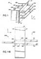
- FIG. 1there is shown a sketch of an electronic system 100 which utilizes a midplane 110 in accordance with the present invention.
- the midplanehas a first side 112 and a second side 114.
- Daughtercards 120A, 120B, 120C and 120Dare electrically connected to the midplane 110 on the second side 114.
- Daughtercards 130A, 130B and 130Care electrically connected to the midplane 110 on the first side 112.
- the daughtercards 130A-130C on the first side 112 of the midplane 110are orthogonal in orientation to the daughtercards 120A-120D on the second side 114 of the midplane 110.
- the concepts embodied in the present inventionare especially applicable to such an orthogonal architecture electronic system.
- FIG. 2shows a preferred embodiment of such an electrical connector assembly 200 in accordance with the present invention.
- Midplane 110includes multiple signal traces that route signals between daughtercards 120A-120D and 130A-130C of the electronic system 100. The midplane 110 is described in greater detail with respect to FIG. 7 . It should be noted that the number of daughtercards 130A-130C shown on the first side 112 and the number of daughtercards 120A-120D shown on the second side 114 are for illustrative purposes only, and the actual number of daughtercards connected to the midplane 110 may vary depending upon the electronic system.
- FIG. 2shows the electrical connector assembly 200 that may be used to connect the daughtercards 120A-120D and 130A-130C to the midplane 110 of FIG. 1 .
- the electrical connector assembly 200is preferably a differential electrical connector assembly.
- the electrical connector assembly 200includes a first differential electrical connector 300, which in the illustration connects to the midplane 110, and a second differential electrical connector 400, which connects to one of the daughtercards (daughtercard 120A is referenced for illustration in FIG. 2 ).
- one or more second connectors 400would be connected to each daughtercard, with the corresponding number of first connectors 300 connected to the midplane 110.
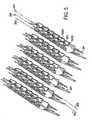
- FIG. 3shows a differential midplane connector 300 having a housing 302, which is preferably made of an insulative material.
- the housing 302has sidewalls 304, 305, end walls 307, 308 and a base (not numbered).
- Disposed in the base of the housing 302are a plurality of signal conductors 310 provided as differential pairs and a plurality of ground conductors 320, with each ground conductor 320 corresponding to a differential pair of signal conductors 310 and positioned adjacent thereto.
- the signal conductors 310 and the ground conductors 320are provided in a plurality of rows. For exemplary purposes only, six rows 330a-330f are shown in FIG.
- each of the rowshaving six differential pairs of signal conductors 310 and six corresponding ground conductors 320.
- the number of rows, the number of signal conductors 310 for each row, and the number of ground conductors 320 for each rowmay be any number as desired. However, as will become more apparent in connection with the description of the midplane 110 in FIG. 8 , it is preferable to pre-select the number of rows, the number of signal conductors 310 for each row, and the number of ground conductors 320 for each row to ensure a substantially square footprint for connecting to the midplane 110.
- Each signal conductor 310has a first contact end 312 connectable to the midplane 110, a second contact end 314, and an intermediate portion 316 therebetween having a first width as measured from first edge 317 to second edge 318 of the signal conductor 310.
- Each ground conductor 320has a first contact end 322 connectable to the midplane 110, a second contact end 324, and an intermediate portion 326 therebetween having a second width as measured from first edge 327 to second edge 328 of the ground conductor 320.
- the second width of the intermediate portion 326 of the ground conductor 320is at least twice the first width of the intermediate portion 316 of the signal conductor 310. This allows the ground conductor 320 to provide sufficient shielding to the corresponding differential pair of signal conductors 310 from the electromagnetic effects of signal conductors in adjacent rows.
- the first contact end 322 of the ground conductor 320includes a first contact arm 332 and a second contact arm 333 spaced from the first contact arm 332.
- the first and second contact arms 332, 333extend in the direction of the corresponding differential pair of signal conductors 310.
- the first and second contact arms 332, 333extend beyond the plane of the corresponding signal conductors 310. This allows the contact arms 332, 333 to provide sufficient shielding to the corresponding differential pair of signal conductors 310 from the electromagnetic effects of adjacent signal conductors in the row.
- the first contact arm 332 of a ground conductor 320is proximal and substantially parallel to the second contact arm 333 of an adjacent ground conductor 320, except at an end of a row.
- first contact end 312 of each signal conductor 310 and the first contact end 322 of each ground conductor 320may take any known form, e.g., pressure-mount contacts, paste-in-hole solder attachment, contact tails adapted for soldering, etc., for connecting to the midplane 110.
- the press-fit contact tails of the signal conductors 310are oriented in a first direction and the press-fit contact tails of the ground conductors 320 are oriented in a second direction substantially perpendicular to the first direction.
- each differential pair of signal conductors 310 of a rowhas one first contact end 312(a) that lies along a first line 350 and is parallel to the plurality of rows and an other first contact end 312(b) that lies along a second line 352 and is parallel to and spaced from the first line 350.
- the first contact end 322 of the corresponding ground conductor 320preferably lies along a third line 354 that is parallel to and spaced from the first and second lines 350, 352.
- the third line 354is positioned between the first and second lines 350, 352.
- the second contact ends 314lie along a fourth line 356.
- the fourth line 356is preferably parallel to the plurality of rows.
- the second contact ends 324 of the ground conductors 320lie along a fifth line 358 that is parallel to and spaced from the fourth line 356.
- FIG. 4Athere is shown an alternative embodiment of FIG. 4 .
- the signal conductors 310are as shown in FIG. 4 .
- a single first ground conductor 370for each row of signal conductors 310.
- the first ground conductor 370extends substantially the length of the corresponding row, where the rows are referenced by 330a'-330f' in FIG. 4A .
- Each first ground conductor 370has a plurality of mating contact ends 374 that are connectable to the corresponding ground conductor of the second differential electrical connector 400.
- the number of mating contact ends 374 of each first ground conductor 370is preferably the same as the number of differential pairs of signal conductors 310 of each corresponding row. In the example illustrated in FIG. 4A , there are six mating contact ends 374 corresponding to the six differential pairs of signal conductors 310.
- a plurality of second ground conductors 380are also provided, with each second ground conductor 380 electrically connected to each first ground conductor 370 and oriented substantially perpendicular to the first ground conductors 370.
- Each second ground conductor 380extends substantially the length of the plurality of rows 330a'-330f', and each second ground conductor 380 is positioned between adjacent differential pairs of signal conductors 310 of each row 330a'-330f.
- the second ground conductors 380are each provided with a first contact end connectable to the midplane 110.
- each second ground conductor 380includes a plurality of contact pins 382 that are oriented perpendicularly to the orientation of the contact pins 312 of the signal conductors 310.
- the contact pins 382 for the rowlie along a third line 354, as described with respect to FIG. 5 .
- Other suitable configurations of signal conductors 310 and ground conductors 320may also be used, as will be apparent to those of ordinary skill in the art.
- the second differential electrical connector 400 of the electrical connector assembly 200which mates to the first differential electrical connector 300 on one side and electrically connects to one of the daughtercards (e.g., daughtercard 130C) on another side.
- the second differential electrical connector 400includes a plurality of wafers 401, where each of the plurality of wafers 401 corresponds to one of the plurality of rows (e.g., 330a-330f of FIG. 4 ) of the first differential electrical connector 300.
- the number of wafers 401 of the second differential electrical connector 400is the same as the number of rows of the first differential electrical connector 300.
- Each wafer 401includes a housing 402, which is preferably made of an insulative material.
- a plurality of signal conductors 410 provided as differential pairsare held in the housing 402 with a corresponding ground conductor 420 positioned adjacent thereto.
- the signal conductors 410 and the corresponding ground conductor 420are shown in greater detail in FIG. 7 . Note that the number of differential pairs of signal conductors 310 provided in a row of the first differential electrical connector 300 is the same as the number of differential pairs of signal conductors 410 provided in the corresponding wafer 401 of the second differential electrical connector 400.
- Each signal conductor 410has a first contact end 412 connectable to one of the daughtercards (e.g., 120A-120D, 130A-130C of FIG. 1 ), a second contact end 414 connectable to the second contact end 314 of a corresponding signal conductor 310 of the first differential electrical connector 300, and an intermediate portion 416 therebetween.
- Each ground conductor 420has a first contact end 422 connectable to the daughtercard, a second contact end 424 connectable to the second contact ends 324 of the corresponding ground conductors 320 of the first differential electrical connector 300, and an intermediate portion 426 therebetween.
- the drawingsshow the first contact end 412 of each signal conductor 410 and the first contact end 422 of the ground conductor 420 as press-fit contact tails.
- first contact ends 412, 422may take any form, e.g., pressure-mount contacts, paste-in-hole solder attachment, contact tails adapted for soldering, etc., for connecting to the daughtercard.
- the ground conductor 420is a ground shield that provides electrical shielding to the corresponding signal conductors 410 of the wafer 401.
- a plurality of ground conductorsmay be utilized instead of a single ground shield, as known in the art.
- slits 430are positioned between adjacent differential pairs of signal conductors 410.
- Each of the slits 430is configured to receive and electrically connect to a ground conductor 440 that is oriented perpendicular to the ground conductor 420 of the wafer 401.
- the ground conductor 440is preferably configured as a ground strip, as shown in FIG. 6 .
- Each ground strip 440electrically connects to each ground conductor 420 of the wafers 401.
- the ground strips 440electrically separate adjacent second contact ends 414 of differential pairs of signal conductors 410.
- the grid-like shielding pattern formed by the ground shields 420 and the ground strips 440provides effective electrical shielding (e.g., from electrical noise) for the differential pairs of signal conductors 410.
- This grid-like shielding pattern formed by the ground shields 420 and the ground strips 440is housed in a shroud 450, which is preferably insulative.
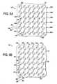
- FIG. 8Athere is shown a top view of a portion of the first side 112 of the midplane 110 of FIG. 1 , with a part of the surface removed to reveal a ground plane layer 150.
- FIG. 8Bshows a top view of the portion (same portion as in FIG. 8A and viewed from the same perspective as FIG. 8A ) of the second side 114 of the midplane 110 of FIG. 1 , with a part of the surface removed to reveal a ground plane layer 170.
- the portion of the midplane 110 shown in FIGS. 8A and 8Bcorrespond to the footprint of a differential electrical connector, such as the differential electrical connector 300, that connects to the midplane 110.
- the portion of the first side 112 of the midplane 110 shown in FIG. 8Aprovides a similar interface for a differential electrical connector as the portion of the second side 114 of the midplane 110 shown in FIG. 8B .
- a midplaneis generally a multi-layer printed circuit board formed of multiple layers of dielectric substrates with signal traces or planes formed on one or more of the dielectric layers. Further, the multi-layer printed circuit board will typically have a ground plane formed on one or more of the dielectric layers. Vias generally extend between layers of a multi-layer printed circuit board. Vias which extend through all layers of a multi-layer printed circuit board are sometimes referred to as through-holes. The vias are usually formed after the layers of substrates are formed into a printed circuit board. Conductive vias generally intersect signal traces on different layers. Conductive vias also interconnect components mounted on the printed circuit board to signal traces on inner layers of the printed circuit board.
- FIG. 8Ashows the ground plane 150, which is formed on one of the dielectric layers of the midplane 110.
- FIG. 8Bshows the ground plane 170, which is formed on one of the dielectric layers of the midplane 110.
- the midplane 110will have more than one ground plane, and ground planes 150, 170 will be different ground planes.
- the ground planes 150, 170may be the same ground plane without departing from the scope of the present invention.
- the midplane 110has a plurality of vias 152, 154 extending from the first side 112 to the second side 114.
- vias 152, 154are through-hole vias.
- the vias 152are signal connecting conductive vias and the vias 154 are ground connecting conductive vias.
- the signal connecting conductive vias 152 on the first side 112 of the midplane 110provide first signal launches 155 for differential pairs of the differential connector connected to the first side 112 and the signal connecting conductive vias 152 on the second side 114 of the midplane 110 provide second signal launches 175 for differential pairs of the differential connector connected to the second side 114.
- the ground connecting conductive vias 154 on the first side 112 of the midplane 110provide first ground launches 157 for differential pairs of the differential connector connected to the first side 112 and the ground connecting conductive vias 154 on the second side 114 of the midplane 110 provide second ground launches 177 for differential pairs of the differential connector connected to the second side 114.
- the first signal launches 155are provided in a plurality of rows 156a-156f, as shown in FIG. 8A , for electrically connecting to a differential connector.
- the six rows 156a-156f showncorrespond to the six rows 330a-330f of differential pairs of signal conductors 310 of the first differential electrical connector 300 shown in FIGS. 4 and 5 .
- Each signal connecting conductive via 152 of a pair corresponding to a differential pair of signal conductorsis electrically isolated from the other signal connecting conductive via 152 of the pair.
- each pair of signal connecting conductive vias 152 corresponding to a differential pair of signal conductorsthere is an area 158 surrounding the pair of signal connecting conductive vias 152 that is free of the ground plane 150.
- This free area 158is sometimes referred to as an "antipad.” It has been found that by ensuring that the area surrounding the pair of signal connecting conductive vias 152 is free of the ground plane 150 (while a region between adjacent pairs of signal connecting conductive vias 152 includes the ground plane 150), there is significantly improved signal performance.
- the antipad 158may take other shapes. See, e.g., U.S. Patent No. 6,607,402 .
- the antipad 158may be substantially rectangular in shape or may be substantially figure-8 in shape.
- one signal connecting conductive via 152 of a pairlies along a first line 160 and the other signal connecting conductive via 152 of the pair lies along a second line 162 that is parallel to and spaced from the first line 160.
- the signal connecting conductive vias 152 of a pairare offset.
- the signal connecting conductive vias 152 of a pairare offset substantially at a forty-five (45) degree angle relative to the orientation of the rows 156a-156f.
- the antipad 158 surrounding the pairis also preferably oriented substantially at a forty-five (45) degree angle relative to the orientation of the rows 156a-156f.
- the first ground launches 157are also provided in the plurality of rows 156a-156f, as shown in FIG. 8A , for electrically connecting to a differential connector.
- the first ground launches 157are provided along a line 164 that is adjacent to and substantially parallel to the first and second lines 160, 162.
- this line 164is spaced between the first and second lines 160, 162.
- the number of first ground launches 157is preferably greater than the number of pairs of first signal launches 155. In the example of FIG. 8A , the number of first ground launches 157 of a row 156a-156f is seven (7), while the number of pairs of first signal launches 155 of a row 156a-156f is six (6).
- FIG. 8Bthere is shown the second signal launches 175 that are provided in a plurality of columns 176a-176f for electrically connecting to a differential connector.
- the six columns 176a-176f showncorrespond to the six rows 330a-330f of differential pairs of signal conductors 310 of the first differential electrical connector 300 shown in FIGS. 4 and 5 .
- These columns 176a-176fare orthogonal to the rows 156a-156f of FIG. 8A .
- This orthogonality of the rows 156a-156f on the first side 112 of the midplane 110 relative to the columns 176a-176f on the second side 114 of the midplane 100corresponds to and accommodates the orthogonality of the daughtercards 130A-130C on the first side 112 relative to the daughtercards 120A-124D on the second side 114 (see FIG. 1 ).
- each signal connecting conductive via 152 of a pair corresponding to a differential pair of signal conductorsis electrically isolated from the other signal connecting conductive via 152 of the pair.
- the through-hole signal connecting conductive vias 152 shown in FIG. 8Aare the same through-hole signal connecting conductive vias 152 shown in FIG. 8B .
- the number of first signal launches 155equals the number of second signal launches 175.
- the midplane design of the present invention(i) significantly reduces the required layers and size of the midplane, (ii) provides for an easier to design and manufacture midplane, (iii) improves the signal characteristics of the transmitted signals, and (iv) significantly reduces the materials and cost of the manufactured midplane.
- each pair of signal connecting conductive vias 152 corresponding to a differential pair of signal conductorsthere is an area 178 surrounding the pair of signal connecting conductive vias 152 that is free of the ground plane 170.
- This antipad 178is similar to the antipad 158 of FIG. 8A . It has been found that by ensuring that the area surrounding the pair of signal connecting conductive vias 152 is free of the ground plane 170 (while a region between adjacent pairs of signal connecting conductive vias 152 includes the ground plane 170), there is significantly improved signal performance.
- the antipad 178may take other shapes.
- the antipad 178may be substantially rectangular in shape or may be substantially figure-8 in shape.
- one signal connecting conductive via 152 of a pairlies along a third line 180 and the other signal connecting conductive via 152 of the pair lies along a fourth line 182 that is parallel to and spaced from the third line 180.
- the signal connecting conductive vias 152 of a pairare offset.
- the signal connecting conductive vias 152 of a pairare offset substantially at a forty-five (45) degree angle relative to the orientation of the columns 176a-176f.
- the antipad 178 surrounding the pairis also preferably oriented substantially at a forty-five (45) degree angle relative to the orientation of the columns 176a-176f.
- the second ground launches 177are also provided in the plurality of columns 176a-176f, as shown in FIG. 8B , for electrically connecting to a differential connector.
- the second ground launches 177are provided along a line 184 that is adjacent to and substantially parallel to the third and fourth lines 180, 182.
- this line 184is spaced between the third and fourth lines 180, 182.
- the columns 176a-176f of the second side 114are orthogonal to the rows 156a-156f of the first side 112.
- the third and fourth lines 180, 182are orthogonal to the first and second lines 160, 162 of FIG. 8A .
- the number of second ground launches 177is preferably greater than the number of pairs of second signal launches 175.
- the number of second ground launches 177 of a column 176a-176fis seven (7), while the number of pairs of second signal launches 175 of a column 176a-176f is six (6).
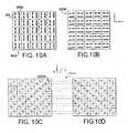
- FIGS. 9A through 9D and FIGS. 10A through 10Dillustrate the advantage of offset contact tails associated with the differential midplane connector 300 according to an embodiment the present invention.
- FIG. 9Aillustrates a cross section through a traditional connector near the second contact end region.
- FIG. 9Ashows that connector 300 has a pair-wise orientation.
- "pair-wise" orientationindicates that the connector is designed with pairs of signal conductors adapted to preferentially electrically couple to each other. For example, the direction of the displacement between one conductor of a pair near the first contact end, e.g., 312(a), and the second conductor of the pair near the first contact end, e.g., 312(b), provides the orientation of the pair.
- a pair-wise orientationis created because the signal conductors of each pairs are oriented in the connector with the signal conductors of a pair displaced from each other in a direction parallel to the shielding.
- the signal conductors of a pairmay be routed closer to each other than to the next nearest signal conductor.
- a pair-wise orientationis desirable for a differential connector because it increases the coupling between the conductors that form a pair and decreases coupling to signal conductors that form an adjacent pair. As a result, each differential signal path is less susceptible to extraneous electromagnetic fields that could induce noise. Further, the coupling between adjacent pairs is reduced, thereby reducing cross-talk within the connector, allowing the connector to operate with greater signal integrity. With greater signal integrity, more signals may be routed through the connector or signals of higher frequency may pass through the connector.
- second contact ends 314A and 314B forming a differential pairare aligned along column 910A.
- Such an alignmentis similar to a connector 300 mounted on surface 112 to receive a connector on board 130A, such as shown in FIG. 1 , with column 910A being aligned along an axis (shown here in the z axis) that is parallel to rows 330a - 330f.
- FIG. 9Cshows a via hole pattern needed to receive first contact ends from signal conductors in a traditional connector mounted as shown in FIG. 9A if offset first contact ends are not used.
- FIG. 9Cshows the hole pattern having the same alignment along an axis as the signal conductors for the connector in FIG. 9A , shown here in the z axis.
- FIG. 9Bshows a cross section of a connector with the second contact ends of a differential pair aligned along row 920A.
- Such an alignmentis similar to a connector 300 mounted on surface 114 to receive a connector on board 120A, such as shown in FIG. 1 , with row 920A being aligned along an axis (shown here in the x axis) that is parallel to rows 330a - 330f.
- board 120Ais perpendicular to board 130A
- the pair-wise orientation and the alignment of the connector in FIG. 9Bis orthogonal to the pair-wise orientation and the alignment of the connector in FIG. 9A .
- FIG. 9Dshows a via hole pattern needed to receive first contact ends from signal conductors in a traditional connector mounted as shown in FIG. 9B if offset first contact ends are not used.
- FIG. 9Dshows the hole pattern having the same alignment along an axis as the signal conductors for the connector in FIG. 9B , shown here in the x axis.
- FIGS. 10A through 10Dillustrates an advantage that can be obtained with offset contact tails, 312(a), 312(b) according to an embodiment of the present invention.
- FIGS. 10A and 10Bshow the second contact ends 314A, 314B and 324A aligned along the same axes (shown here in the z and x axes, respectively) as previously shown in FIGS. 9A and 9B .
- a forty-five (45) degree offsetassociated with the orientation of the contact tails 312(a), 312(b) from the second contact end position, there is a corresponding forty-five (45) degree offset for hole patterns associated with each differential pair.
- FIGS. 10C and 10Dshow via hole patterns needed to receive first contact ends 312(a) and 312(b) from signal conductors 310 as mounted in FIGS. 10A and 10B , respectively.
- FIG. 10Cshows the hole pattern having an alignment along an axis z' that has an angle about forty-five degrees from the alignment (shown here in the z axis) of the second contact ends, 314 as shown in FIG. 10A .
- FIG. 10Dshows the hole pattern having an alignment along an axis x' that has an angle about forty-five degrees from the alignment (shown here in the x axis) of the second contact ends, 314 as shown in FIG. 10B .
- the holes for differential pairs on opposing sides of midplane 110have the same pattern and may be aligned. If the hole patterns on opposite sides of the midplane align, connectors in opposite sides of the midplane may be inserted into the same vias.
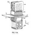
- FIG. 11Ashows connectors 300A and 300B mounted on opposite sides of midplane 110.
- Connector 300Amates with connector 400A.
- Connector 300Bmates with connector 400B.
- connectors 400A and 400Bare attached to printed circuit boards that are mounted with different orientations, the pair-wise orientation of connectors 400A and 400B have different orientations.
- connectors 400A and 400Bare mounted orthogonal to each other.
- connectors 300A and 300Bmust similarly be mounted orthogonal to each other. Consequently, connector 300A has a pair-wise orientation and alignment and connector 300B has a pair-wise orientation and alignment.
- the offset pattern of contact tails 312allows the contact tails 312 of connectors 300A and 300B to be mounted using one set of via holes. Further, every pair of signal conductors in connector 300A may be mounted in the same two vias as a pair of signal conductors in connector 300B.
- FIG. 11Bis a side view of a pair of signal conductors within connectors 300A and 300B mounted on opposing sides of a midplane 110.
- the signal conductorshave an orientation and alignment on one side of the board and an orientation and alignment on the opposing side. Despite orthogonal orientations, the offset of the contact tails of both pairs allows the contact tails to align so that they may be connected through vias 1110a and 1110b, respectively.
- each connectormay be constructed with shielding, signal conductor positioning or other structures that provide a pair-wise orientation that increases the signal integrity when carrying differential signals.
- connections between the signal conductors on opposing sides of the midplanemay be made using only the vias of the midplane to carry the signal.
- No traces within the midplaneare needed to carry differential signals from one side of the midplane to another. Eliminating traces, and transitions between vias and traces, within the midplane means less distortion of the signal occurs in the midplane, further increasing the signal integrity of the connector.
- FIG. 8A and 8Billustrate that ground clearances around differential pairs may be structured to further improve the integrity of signals passing through the midplane oriented as differential pairs.
Landscapes
- Engineering & Computer Science (AREA)
- Microelectronics & Electronic Packaging (AREA)
- Details Of Connecting Devices For Male And Female Coupling (AREA)
- Cable Transmission Systems, Equalization Of Radio And Reduction Of Echo (AREA)
- Structure Of Printed Boards (AREA)
- Combinations Of Printed Boards (AREA)
Description
- Modem electronic systems are typically assembled from multiple printed circuit boards. Such printed circuit boards, which are commonly referred to as "daughter cards", contain components thereon, such as integrated circuits. Each daughter card also typically includes one or more connectors that allow the components on the daughter card to communicate with components on the other daughter cards in the system.
- One way to interconnect the daughter cards in an electronic system is to utilize a midplane. A midplane is a printed circuit board, typically larger than the daughter cards, to which the daughter cards are connected -- by way of connectors on both the daughter cards and the midplane -- and that provides conductive paths therein. The conductive paths, which are also referred to as "signal traces", interconnect and provide communication between the daughter cards in the system. A midplane, as the name implies, provides connectors on both sides, allowing daughter cards to be connected on both sides of the midplane. The midplane can route signals between daughter cards connected on the same side of the midplane or can cross-connect a daughter card on one side of the midplane with a daughter card on the other side of the midplane.
- In order to connect a connector to the midplane, holes are conventionally drilled through the midplane. The holes, which are also referred to as "vias", electrically connect to signal traces in the midplane. The inside walls of the vias are typically plated with a conductive material, such as metal, to provide electrical conductivity. The connector is provided with contact ends, such as press-fit contact tails or SMT (surface mount technique) contact tails, for connecting to the vias.
- As electronic systems have become smaller, faster and more complex, this has generally required that midplanes provide more vias and signal traces without increasing in size, or in many instances, while actually decreasing in size. This has introduced significant difficulties in designing and fabricating midplanes, as well as significant difficulties in dealing with electrical noise and other electrical characteristics. Electrical noise is usually considered any undesirable electrical energy in an electronic system, including but not limited to, reflections, electromagnetic interference, mode conversions and unwanted coupling, such as cross-talk.
- The trend for smaller, faster and more complex electronic systems has also required connectors to carry more and faster data signals in a smaller space without degrading the electrical characteristics of the signal. Connectors can be made to carry more signals in less space by placing signal conductors in a connector closer together. A major difficulty with placing signal conductors closer together is that electrical noise between the signal conductors increases as the distance between signal conductors decreases and as the speed of the signals increases. In addition, as frequency content increases, there is a greater possibility of energy loss. Energy loss may be attributed to impedance discontinuities, mode conversion, leakage from imperfect shielding, or undesired coupling to other conductors (crosstalk). Therefore, connectors are designed to control the mechanisms that enable energy loss. Conductors composing transmission paths are designed to match system impedance, enforce a known propagating mode of energy, minimize eddy currents, and isolate alternate transmission paths from one another. One example of controlling energy loss is the placement of a conductor connected to a ground placed adjacent to a signal contact element to determine an impedance and minimize energy loss in the form of radiation.
- One way to control electrical noise in a connector is to utilize differential signals. Differential signals are signals represented by a pair of signal conductors, called a "differential pair". The voltage difference between the pair of signal conductors represents the signal. If electrical noise is electromagnetically coupled to a differential pair, the effect on each signal conductor of the pair should be similar. This renders a differential pair less sensitive to electrical noise as compared with a single signal conductor. However, use of a differential connector, especially in a midplane system architecture, introduces further difficulties as vias corresponding to the differential pair on either side of the midplane must each be electrically connected in the midplane and signal traces can only be routed between adjacent differential pairs.
- What is desired, therefore, is to provide a midplane and a differential connector designed for such a midplane that addresses the difficulties described above.
- In one embodiment of a midplane in accordance with the invention, the midplane has a first side to which contact ends of a first differential connector are connected and a second side opposite the first side to which contact ends of a second differential connector are connected. The midplane includes a plurality of vias extending from the first side to the second side, with the vias providing first signal launches on the first side and second signal launches on the second side. The first signal launches are provided in a plurality of rows for electrically connecting to the contact ends of the first differential connector, with each row having first signal launches along a first line and first signal launches along a second line substantially parallel to the first line. The first signal launches along the first and second lines are offset so that first signal launches along the first line and adjacent first signal launches along the second line correspond to differential pairs of the first differential connector. The second signal launches are provided in a plurality of columns for electrically connecting to the contact ends of the second differential connector, with each column having second signal launches along a third line and second signal launches along a fourth line substantially parallel to the third line. The second signal launches along the third and fourth lines are offset so that second signal launches along the third line and adjacent second signal launches along the fourth line correspond to differential pairs of the second differential connector.
- The accompanying drawings are not intended to be drawn to scale. In the drawings, each identical or nearly identical component that is illustrated in various figures is represented by a like numeral. For purposes of clarity, not every component may be labeled in every drawing. In the drawings:
FIG. 1 is a perspective view of an electronic system utilizing a midplane according to an embodiment of the present invention;FIG. 2 is a partially exploded view of a differential electrical connector assembly according to an embodiment of the present invention that may be used in the electronic system ofFIG. 1 ;FIG. 3 is a perspective view of a differential midplane connector shown inFIG. 2 ;FIG. 4 is a perspective view showing rows of differential pair signal conductors and corresponding ground conductors of the differential midplane connector shown inFIG. 3 according to an embodiment of the present invention;FIG. 4A is an alternative embodiment ofFIG. 4 , showing rows of differential pair signal conductors and corresponding ground conductors of the differential midplane connector shown inFIG. 3 ;FIG. 5 is a bottom view showing first contact ends of the differential pair signal conductors and corresponding ground conductors of the differential midplane connector shown inFIG. 4 ;FIG. 6 is a perspective view of a differential daughtercard connector according to an embodiment of the present invention shown inFIG. 2 , with a wafer separated from the connector for clarity;FIG. 7 is an exploded view of the wafer ofFIG. 6 showing only the differential pair signal conductors and corresponding ground conductor;FIG. 8A is a schematic top view of a portion of one side of the midplane ofFIG. 1 , with a part of the surface removed to show a ground plane layer;FIG. 8B is a schematic top view of a portion (the same portion asFIG. 8A ) of the other side of the midplane ofFIG. 1 , with a part of the surface removed to show a ground plane layer;FIG. 9A is a schematic view of a cross-section through the mating contact region of a traditional differential midplane connector attached to one side of a midplane;FIG. 9B is a schematic view of a cross-section through the mating contact region of a traditional differential midplane connector attached to the other side of a midplane as illustrated inFIG. 9A ;FIGS. 9C and 9D are diagrams illustrating via hole patterns forFIGS. 9A and 9B , respectively for traditional differential midplane connectors;FIG. 10A is a schematic view of a cross-section through the mating contact region of a differential midplane connector attached to one side of a midplane according to an embodiment of the present invention;FIG. 10B is a schematic view of a cross-section through the mating contact region of a differential midplane connector attached to the other side of a midplane according to an embodiment of the present invention;FIGS. 10C and 10D are diagrams illustrating via hole patterns forFIGS. 10A and 10B , respectively for differential midplane connectors according to an embodiment of the present invention;FIG. 11A is a perspective view of two differential electrical connector assemblies attached to opposing sides of a midplane according to an embodiment of the present invention; andFIG. 11B is a schematic side view ofFIG. 11A , showing two pairs of signal conductors each mounted on opposing sides of a midplane and sharing common vias according to an embodiment of the present invention.- This invention is not limited in its application to the details of construction and the arrangement of components set forth in the following description or illustrated in the drawings. The invention is capable of other embodiments and of being practiced or of being carried out in various ways. Also, the phraseology and terminology used herein is for the purpose of description and should not be regarded as limiting. The use of "including," "comprising," "having," "containing," "involving," and variations thereof herein, is meant to encompass the items listed thereafter and equivalents thereof as well as additional items.
- Referring to
FIG. 1 , there is shown a sketch of anelectronic system 100 which utilizes amidplane 110 in accordance with the present invention. The midplane has afirst side 112 and asecond side 114.Daughtercards midplane 110 on thesecond side 114.Daughtercards midplane 110 on thefirst side 112. Note that thedaughtercards 130A-130C on thefirst side 112 of themidplane 110 are orthogonal in orientation to thedaughtercards 120A-120D on thesecond side 114 of themidplane 110. The concepts embodied in the present invention are especially applicable to such an orthogonal architecture electronic system. - While not shown in the sketch of
FIG. 1 ,daughtercards 120A-120D and 130A-130C are electrically connected to themidplane 110 by electrical connector assemblies.FIG. 2 shows a preferred embodiment of such anelectrical connector assembly 200 in accordance with the present invention.Midplane 110 includes multiple signal traces that route signals betweendaughtercards 120A-120D and 130A-130C of theelectronic system 100. Themidplane 110 is described in greater detail with respect toFIG. 7 . It should be noted that the number ofdaughtercards 130A-130C shown on thefirst side 112 and the number ofdaughtercards 120A-120D shown on thesecond side 114 are for illustrative purposes only, and the actual number of daughtercards connected to themidplane 110 may vary depending upon the electronic system. FIG. 2 shows theelectrical connector assembly 200 that may be used to connect thedaughtercards 120A-120D and 130A-130C to themidplane 110 ofFIG. 1 . Theelectrical connector assembly 200 is preferably a differential electrical connector assembly. Theelectrical connector assembly 200 includes a first differentialelectrical connector 300, which in the illustration connects to themidplane 110, and a second differentialelectrical connector 400, which connects to one of the daughtercards (daughtercard 120A is referenced for illustration inFIG. 2 ). Typically, one or moresecond connectors 400 would be connected to each daughtercard, with the corresponding number offirst connectors 300 connected to themidplane 110.FIG. 3 shows adifferential midplane connector 300 having ahousing 302, which is preferably made of an insulative material. Thehousing 302 has sidewalls 304, 305, endwalls housing 302 are a plurality ofsignal conductors 310 provided as differential pairs and a plurality ofground conductors 320, with eachground conductor 320 corresponding to a differential pair ofsignal conductors 310 and positioned adjacent thereto. As shown in greater detail inFIGS. 4 ,4A and5 , thesignal conductors 310 and theground conductors 320 are provided in a plurality of rows. For exemplary purposes only, sixrows 330a-330f are shown inFIG. 4 , with each of the rows having six differential pairs ofsignal conductors 310 and sixcorresponding ground conductors 320. Note that the number of rows, the number ofsignal conductors 310 for each row, and the number ofground conductors 320 for each row may be any number as desired. However, as will become more apparent in connection with the description of themidplane 110 inFIG. 8 , it is preferable to pre-select the number of rows, the number ofsignal conductors 310 for each row, and the number ofground conductors 320 for each row to ensure a substantially square footprint for connecting to themidplane 110.- Each
signal conductor 310 has afirst contact end 312 connectable to themidplane 110, asecond contact end 314, and anintermediate portion 316 therebetween having a first width as measured fromfirst edge 317 tosecond edge 318 of thesignal conductor 310. Eachground conductor 320 has afirst contact end 322 connectable to themidplane 110, asecond contact end 324, and anintermediate portion 326 therebetween having a second width as measured fromfirst edge 327 tosecond edge 328 of theground conductor 320. Preferably, the second width of theintermediate portion 326 of theground conductor 320 is at least twice the first width of theintermediate portion 316 of thesignal conductor 310. This allows theground conductor 320 to provide sufficient shielding to the corresponding differential pair ofsignal conductors 310 from the electromagnetic effects of signal conductors in adjacent rows. - In the preferred embodiment, the
first contact end 322 of theground conductor 320 includes afirst contact arm 332 and asecond contact arm 333 spaced from thefirst contact arm 332. The first andsecond contact arms signal conductors 310. Preferably, the first andsecond contact arms corresponding signal conductors 310. This allows thecontact arms signal conductors 310 from the electromagnetic effects of adjacent signal conductors in the row. Note that for each of the plurality ofrows 330a-330f, thefirst contact arm 332 of aground conductor 320 is proximal and substantially parallel to thesecond contact arm 333 of anadjacent ground conductor 320, except at an end of a row. - The drawings show that the
first contact end 312 of eachsignal conductor 310 and thefirst contact end 322 of eachground conductor 320 as press-fit contact tails. However, it should be apparent to one of ordinary skill in the art that the first contact ends 312, 322 may take any known form, e.g., pressure-mount contacts, paste-in-hole solder attachment, contact tails adapted for soldering, etc., for connecting to themidplane 110. In the preferred embodiment, the press-fit contact tails of thesignal conductors 310 are oriented in a first direction and the press-fit contact tails of theground conductors 320 are oriented in a second direction substantially perpendicular to the first direction. - Referring to
FIGS. 4 and5 , each differential pair ofsignal conductors 310 of a row, e.g.,row 330a, has one first contact end 312(a) that lies along afirst line 350 and is parallel to the plurality of rows and an other first contact end 312(b) that lies along asecond line 352 and is parallel to and spaced from thefirst line 350. Thefirst contact end 322 of thecorresponding ground conductor 320 preferably lies along athird line 354 that is parallel to and spaced from the first andsecond lines third line 354 is positioned between the first andsecond lines midplane 110 inFIG. 8 , provides a substantially square footprint for connecting to themidplane 110. - For each differential pair of
signal conductors 310 of a row, the second contact ends 314 lie along afourth line 356. Thefourth line 356 is preferably parallel to the plurality of rows. The second contact ends 324 of theground conductors 320 lie along afifth line 358 that is parallel to and spaced from thefourth line 356. - Referring now to
FIG. 4A , there is shown an alternative embodiment ofFIG. 4 . In this embodiment, thesignal conductors 310 are as shown inFIG. 4 . However, instead of providing aground conductor 320 corresponding to each differential pair ofsignal conductors 310 as illustrated inFIG. 4 , there is provided a singlefirst ground conductor 370 for each row ofsignal conductors 310. Thefirst ground conductor 370 extends substantially the length of the corresponding row, where the rows are referenced by 330a'-330f' inFIG. 4A . Eachfirst ground conductor 370 has a plurality of mating contact ends 374 that are connectable to the corresponding ground conductor of the second differentialelectrical connector 400. The number of mating contact ends 374 of eachfirst ground conductor 370 is preferably the same as the number of differential pairs ofsignal conductors 310 of each corresponding row. In the example illustrated inFIG. 4A , there are six mating contact ends 374 corresponding to the six differential pairs ofsignal conductors 310. - A plurality of
second ground conductors 380 are also provided, with eachsecond ground conductor 380 electrically connected to eachfirst ground conductor 370 and oriented substantially perpendicular to thefirst ground conductors 370. Eachsecond ground conductor 380 extends substantially the length of the plurality ofrows 330a'-330f', and eachsecond ground conductor 380 is positioned between adjacent differential pairs ofsignal conductors 310 of eachrow 330a'-330f. Thesecond ground conductors 380 are each provided with a first contact end connectable to themidplane 110. Preferably, the first contact end of eachsecond ground conductor 380 includes a plurality of contact pins 382 that are oriented perpendicularly to the orientation of the contact pins 312 of thesignal conductors 310. Note that for eachrow 330a'-330f, there is acontact pin 382 of asecond ground conductor 380 adjacent each differential pair ofsignal conductors 310. And for eachrow 330a'-330f, the contact pins 382 for the row lie along athird line 354, as described with respect toFIG. 5 . Other suitable configurations ofsignal conductors 310 andground conductors 320 may also be used, as will be apparent to those of ordinary skill in the art. - Referring now to
FIGS. 6 and7 , there is shown the second differentialelectrical connector 400 of theelectrical connector assembly 200 which mates to the first differentialelectrical connector 300 on one side and electrically connects to one of the daughtercards (e.g.,daughtercard 130C) on another side. The second differentialelectrical connector 400 includes a plurality ofwafers 401, where each of the plurality ofwafers 401 corresponds to one of the plurality of rows (e.g., 330a-330f ofFIG. 4 ) of the first differentialelectrical connector 300. Thus, the number ofwafers 401 of the second differentialelectrical connector 400 is the same as the number of rows of the first differentialelectrical connector 300. Eachwafer 401 includes ahousing 402, which is preferably made of an insulative material. A plurality ofsignal conductors 410 provided as differential pairs are held in thehousing 402 with acorresponding ground conductor 420 positioned adjacent thereto. Thesignal conductors 410 and thecorresponding ground conductor 420 are shown in greater detail inFIG. 7 . Note that the number of differential pairs ofsignal conductors 310 provided in a row of the first differentialelectrical connector 300 is the same as the number of differential pairs ofsignal conductors 410 provided in thecorresponding wafer 401 of the second differentialelectrical connector 400. - Each
signal conductor 410 has afirst contact end 412 connectable to one of the daughtercards (e.g., 120A-120D, 130A-130C ofFIG. 1 ), asecond contact end 414 connectable to thesecond contact end 314 of acorresponding signal conductor 310 of the first differentialelectrical connector 300, and anintermediate portion 416 therebetween. Eachground conductor 420 has afirst contact end 422 connectable to the daughtercard, asecond contact end 424 connectable to the second contact ends 324 of thecorresponding ground conductors 320 of the first differentialelectrical connector 300, and anintermediate portion 426 therebetween. The drawings show thefirst contact end 412 of eachsignal conductor 410 and thefirst contact end 422 of theground conductor 420 as press-fit contact tails. However, it should be apparent to one of ordinary skill in the art that the first contact ends 412, 422 may take any form, e.g., pressure-mount contacts, paste-in-hole solder attachment, contact tails adapted for soldering, etc., for connecting to the daughtercard. - In the preferred embodiment, the
ground conductor 420 is a ground shield that provides electrical shielding to thecorresponding signal conductors 410 of thewafer 401. However, a plurality of ground conductors may be utilized instead of a single ground shield, as known in the art. Provided in thesecond contact end 424 of theground shield 420 areslits 430. Preferably, theslits 430 are positioned between adjacent differential pairs ofsignal conductors 410. - Each of the
slits 430 is configured to receive and electrically connect to aground conductor 440 that is oriented perpendicular to theground conductor 420 of thewafer 401. Note that theground conductor 440 is preferably configured as a ground strip, as shown inFIG. 6 . Eachground strip 440 electrically connects to eachground conductor 420 of thewafers 401. In this manner, the ground strips 440 electrically separate adjacent second contact ends 414 of differential pairs ofsignal conductors 410. The grid-like shielding pattern formed by the ground shields 420 and the ground strips 440 provides effective electrical shielding (e.g., from electrical noise) for the differential pairs ofsignal conductors 410. This grid-like shielding pattern formed by the ground shields 420 and the ground strips 440 is housed in ashroud 450, which is preferably insulative. - Referring now to
FIG. 8A , there is shown a top view of a portion of thefirst side 112 of themidplane 110 ofFIG. 1 , with a part of the surface removed to reveal aground plane layer 150.FIG. 8B shows a top view of the portion (same portion as inFIG. 8A and viewed from the same perspective asFIG. 8A ) of thesecond side 114 of themidplane 110 ofFIG. 1 , with a part of the surface removed to reveal aground plane layer 170. The portion of themidplane 110 shown inFIGS. 8A and 8B correspond to the footprint of a differential electrical connector, such as the differentialelectrical connector 300, that connects to themidplane 110. Note that the portion of thefirst side 112 of themidplane 110 shown inFIG. 8A provides a similar interface for a differential electrical connector as the portion of thesecond side 114 of themidplane 110 shown inFIG. 8B . - As known in the art, a midplane is generally a multi-layer printed circuit board formed of multiple layers of dielectric substrates with signal traces or planes formed on one or more of the dielectric layers. Further, the multi-layer printed circuit board will typically have a ground plane formed on one or more of the dielectric layers. Vias generally extend between layers of a multi-layer printed circuit board. Vias which extend through all layers of a multi-layer printed circuit board are sometimes referred to as through-holes. The vias are usually formed after the layers of substrates are formed into a printed circuit board. Conductive vias generally intersect signal traces on different layers. Conductive vias also interconnect components mounted on the printed circuit board to signal traces on inner layers of the printed circuit board.
FIG. 8A shows theground plane 150, which is formed on one of the dielectric layers of themidplane 110.FIG. 8B shows theground plane 170, which is formed on one of the dielectric layers of themidplane 110. Typically, themidplane 110 will have more than one ground plane, andground planes midplane 110 has a plurality ofvias first side 112 to thesecond side 114. Thus, vias 152, 154 are through-hole vias. Thevias 152 are signal connecting conductive vias and thevias 154 are ground connecting conductive vias. Note that the signal connectingconductive vias 152 on thefirst side 112 of themidplane 110 provide first signal launches 155 for differential pairs of the differential connector connected to thefirst side 112 and the signal connectingconductive vias 152 on thesecond side 114 of themidplane 110 provide second signal launches 175 for differential pairs of the differential connector connected to thesecond side 114. The ground connectingconductive vias 154 on thefirst side 112 of themidplane 110 provide first ground launches 157 for differential pairs of the differential connector connected to thefirst side 112 and the ground connectingconductive vias 154 on thesecond side 114 of themidplane 110 provide second ground launches 177 for differential pairs of the differential connector connected to thesecond side 114.- The first signal launches 155 are provided in a plurality of
rows 156a-156f, as shown inFIG. 8A , for electrically connecting to a differential connector. In the example ofFIG. 8A , the sixrows 156a-156f shown correspond to the sixrows 330a-330f of differential pairs ofsignal conductors 310 of the first differentialelectrical connector 300 shown inFIGS. 4 and5 . Each signal connecting conductive via 152 of a pair corresponding to a differential pair of signal conductors is electrically isolated from the other signal connecting conductive via 152 of the pair. Further, for each pair of signal connectingconductive vias 152 corresponding to a differential pair of signal conductors, there is anarea 158 surrounding the pair of signal connectingconductive vias 152 that is free of theground plane 150. Thisfree area 158 is sometimes referred to as an "antipad." It has been found that by ensuring that the area surrounding the pair of signal connectingconductive vias 152 is free of the ground plane 150 (while a region between adjacent pairs of signal connectingconductive vias 152 includes the ground plane 150), there is significantly improved signal performance. Note that while the preferred embodiment of the invention illustrates a substantiallyoval antipad 158, theantipad 158 may take other shapes. See, e.g.,U.S. Patent No. 6,607,402 . For example, theantipad 158 may be substantially rectangular in shape or may be substantially figure-8 in shape. - As with the first contact ends 312 of each differential pair of
signal conductors 310 of the first differential electrical connector 300 (FIGS. 4 and5 ), one signal connecting conductive via 152 of a pair lies along afirst line 160 and the other signal connecting conductive via 152 of the pair lies along asecond line 162 that is parallel to and spaced from thefirst line 160. Also, as with the first contact ends 312 of each differential pair ofsignal conductors 310 of the first differentialelectrical connector 300, the signal connectingconductive vias 152 of a pair are offset. Preferably, the signal connectingconductive vias 152 of a pair are offset substantially at a forty-five (45) degree angle relative to the orientation of therows 156a-156f. Note that because of this offset of the signal connectingconductive vias 152 of a pair, theantipad 158 surrounding the pair is also preferably oriented substantially at a forty-five (45) degree angle relative to the orientation of therows 156a-156f. - The first ground launches 157 are also provided in the plurality of
rows 156a-156f, as shown inFIG. 8A , for electrically connecting to a differential connector. For each of therows 156a-156f, the first ground launches 157 are provided along aline 164 that is adjacent to and substantially parallel to the first andsecond lines line 164 is spaced between the first andsecond lines rows 156a-156f, the number of first ground launches 157 is preferably greater than the number of pairs of first signal launches 155. In the example ofFIG. 8A , the number of first ground launches 157 of arow 156a-156f is seven (7), while the number of pairs of first signal launches 155 of arow 156a-156f is six (6). - Referring now to
FIG. 8B , there is shown the second signal launches 175 that are provided in a plurality of columns 176a-176f for electrically connecting to a differential connector. In the exemplary illustration ofFIG. 8B , the six columns 176a-176f shown correspond to the sixrows 330a-330f of differential pairs ofsignal conductors 310 of the first differentialelectrical connector 300 shown inFIGS. 4 and5 . These columns 176a-176f are orthogonal to therows 156a-156f ofFIG. 8A . This orthogonality of therows 156a-156f on thefirst side 112 of themidplane 110 relative to the columns 176a-176f on thesecond side 114 of themidplane 100 corresponds to and accommodates the orthogonality of thedaughtercards 130A-130C on thefirst side 112 relative to thedaughtercards 120A-124D on the second side 114 (seeFIG. 1 ). - Same as in
FIG. 8A , each signal connecting conductive via 152 of a pair corresponding to a differential pair of signal conductors is electrically isolated from the other signal connecting conductive via 152 of the pair. In fact, the through-hole signal connectingconductive vias 152 shown inFIG. 8A are the same through-hole signal connectingconductive vias 152 shown inFIG. 8B . Thus, for the portion of themidplane 110 shown inFIGS. 8A and 8B , the number of first signal launches 155 equals the number of second signal launches 175. Note that by designing a differential electrical connector that provides a substantially square footprint for connecting to the midplane 110 (such as the first differential electrical connector 300), it is possible to provide themidplane 110 that utilizes the same through-hole signal connectingconductive vias 152 for connecting a differential electrical connector to thefirst side 112 and a differential electrical connector to thesecond side 114. In this manner, the midplane design of the present invention (i) significantly reduces the required layers and size of the midplane, (ii) provides for an easier to design and manufacture midplane, (iii) improves the signal characteristics of the transmitted signals, and (iv) significantly reduces the materials and cost of the manufactured midplane. - For each pair of signal connecting
conductive vias 152 corresponding to a differential pair of signal conductors, there is anarea 178 surrounding the pair of signal connectingconductive vias 152 that is free of theground plane 170. Thisantipad 178 is similar to theantipad 158 ofFIG. 8A . It has been found that by ensuring that the area surrounding the pair of signal connectingconductive vias 152 is free of the ground plane 170 (while a region between adjacent pairs of signal connectingconductive vias 152 includes the ground plane 170), there is significantly improved signal performance. Note that while the preferred embodiment of the invention illustrates a substantiallyoval antipad 178, theantipad 178 may take other shapes. For example, theantipad 178 may be substantially rectangular in shape or may be substantially figure-8 in shape. - As with the first contact ends 312 of each differential pair of
signal conductors 310 of the first differential electrical connector 300 (FIGS. 4 and5 ), one signal connecting conductive via 152 of a pair lies along athird line 180 and the other signal connecting conductive via 152 of the pair lies along afourth line 182 that is parallel to and spaced from thethird line 180. Also, as with the first contact ends 312 of each differential pair ofsignal conductors 310 of the first differentialelectrical connector 300, the signal connectingconductive vias 152 of a pair are offset. Preferably, the signal connectingconductive vias 152 of a pair are offset substantially at a forty-five (45) degree angle relative to the orientation of the columns 176a-176f. Note that because of this offset of the signal connectingconductive vias 152 of a pair, theantipad 178 surrounding the pair is also preferably oriented substantially at a forty-five (45) degree angle relative to the orientation of the columns 176a-176f. - The second ground launches 177 are also provided in the plurality of columns 176a-176f, as shown in
FIG. 8B , for electrically connecting to a differential connector. For each of the columns 176a-176f, the second ground launches 177 are provided along aline 184 that is adjacent to and substantially parallel to the third andfourth lines line 184 is spaced between the third andfourth lines second side 114 are orthogonal to therows 156a-156f of thefirst side 112. Thus, the third andfourth lines second lines FIG. 8A . For each of the columns 176a-176f, the number of second ground launches 177 is preferably greater than the number of pairs of second signal launches 175. In the example ofFIG. 8B , the number of second ground launches 177 of a column 176a-176f is seven (7), while the number of pairs of second signal launches 175 of a column 176a-176f is six (6). FIGS. 9A through 9D andFIGS. 10A through 10D illustrate the advantage of offset contact tails associated with thedifferential midplane connector 300 according to an embodiment the present invention.FIG. 9A illustrates a cross section through a traditional connector near the second contact end region.FIG. 9A shows thatconnector 300 has a pair-wise orientation. As used herein, "pair-wise" orientation indicates that the connector is designed with pairs of signal conductors adapted to preferentially electrically couple to each other. For example, the direction of the displacement between one conductor of a pair near the first contact end, e.g., 312(a), and the second conductor of the pair near the first contact end, e.g., 312(b), provides the orientation of the pair.- Multiple design techniques may be used to create a pair-wise orientation of a connector. These design techniques may be used alone or in combination. In the illustrated embodiment, shields are used to create preferential coupling between pairs. A pair-wise orientation is created because the signal conductors of each pairs are oriented in the connector with the signal conductors of a pair displaced from each other in a direction parallel to the shielding.
- As another example of a technique to create a pair-wise orientation, the signal conductors of a pair may be routed closer to each other than to the next nearest signal conductor.
- A pair-wise orientation is desirable for a differential connector because it increases the coupling between the conductors that form a pair and decreases coupling to signal conductors that form an adjacent pair. As a result, each differential signal path is less susceptible to extraneous electromagnetic fields that could induce noise. Further, the coupling between adjacent pairs is reduced, thereby reducing cross-talk within the connector, allowing the connector to operate with greater signal integrity. With greater signal integrity, more signals may be routed through the connector or signals of higher frequency may pass through the connector.
- In
FIG. 9A , second contact ends 314A and 314B forming a differential pair are aligned alongcolumn 910A. Such an alignment is similar to aconnector 300 mounted onsurface 112 to receive a connector onboard 130A, such as shown inFIG. 1 , withcolumn 910A being aligned along an axis (shown here in the z axis) that is parallel torows 330a - 330f. FIG. 9C shows a via hole pattern needed to receive first contact ends from signal conductors in a traditional connector mounted as shown inFIG. 9A if offset first contact ends are not used.FIG. 9C shows the hole pattern having the same alignment along an axis as the signal conductors for the connector inFIG. 9A , shown here in the z axis.FIG. 9B shows a cross section of a connector with the second contact ends of a differential pair aligned alongrow 920A. Such an alignment is similar to aconnector 300 mounted onsurface 114 to receive a connector onboard 120A, such as shown inFIG. 1 , withrow 920A being aligned along an axis (shown here in the x axis) that is parallel torows 330a - 330f. Becauseboard 120A is perpendicular to board 130A, the pair-wise orientation and the alignment of the connector inFIG. 9B is orthogonal to the pair-wise orientation and the alignment of the connector inFIG. 9A .FIG. 9D shows a via hole pattern needed to receive first contact ends from signal conductors in a traditional connector mounted as shown inFIG. 9B if offset first contact ends are not used.FIG. 9D shows the hole pattern having the same alignment along an axis as the signal conductors for the connector inFIG. 9B , shown here in the x axis.- When the via hole patterns of
FIG. 9C and 9D are formed on opposite sides of a midplane, no amount of shifting of the hole pattern allows both holes for the same pair to be aligned. For example, ifholes FIGS. 10A through 10D illustrates an advantage that can be obtained with offset contact tails, 312(a), 312(b) according to an embodiment of the present invention.FIGS. 10A and 10B show the second contact ends 314A, 314B and 324A aligned along the same axes (shown here in the z and x axes, respectively) as previously shown inFIGS. 9A and 9B . With a forty-five (45) degree offset associated with the orientation of the contact tails 312(a), 312(b) from the second contact end position, there is a corresponding forty-five (45) degree offset for hole patterns associated with each differential pair. Thus,FIGS. 10C and 10D show via hole patterns needed to receive first contact ends 312(a) and 312(b) fromsignal conductors 310 as mounted inFIGS. 10A and 10B , respectively.FIG. 10C shows the hole pattern having an alignment along an axis z' that has an angle about forty-five degrees from the alignment (shown here in the z axis) of the second contact ends, 314 as shown inFIG. 10A . Similarly,FIG. 10D shows the hole pattern having an alignment along an axis x' that has an angle about forty-five degrees from the alignment (shown here in the x axis) of the second contact ends, 314 as shown inFIG. 10B . As a result, even though themating contact portions 314 ofconnectors 300 on opposing sides ofmidplane 110 have orthogonal pair-wise orientations and alignments, the holes for differential pairs on opposing sides ofmidplane 110 have the same pattern and may be aligned. If the hole patterns on opposite sides of the midplane align, connectors in opposite sides of the midplane may be inserted into the same vias.- This alignment is shown in
FIG. 11A , which showsconnectors midplane 110.Connector 300A mates withconnector 400A.Connector 300B mates withconnector 400B. Becauseconnectors connectors connectors connectors connectors connector 300A has a pair-wise orientation and alignment andconnector 300B has a pair-wise orientation and alignment. - Despite the different pair-wise orientations of
connectors contact tails 312 allows thecontact tails 312 ofconnectors connector 300A may be mounted in the same two vias as a pair of signal conductors inconnector 300B. FIG. 11B is a side view of a pair of signal conductors withinconnectors midplane 110. The signal conductors have an orientation and alignment on one side of the board and an orientation and alignment on the opposing side. Despite orthogonal orientations, the offset of the contact tails of both pairs allows the contact tails to align so that they may be connected through vias 1110a and 1110b, respectively.- In this way, the two signals that form one differential signal are routed together from a daughter card on one side of
midplane 110, through a first set of connectors tomidplane 110, throughmidplane 110 to a second set of connectors to a second daughter card. The two signal conductors are kept together as a pair, thereby providing desirable signal integrity properties. Further, the transmission path may be optimized for carrying differential signals. As described above, each connector may be constructed with shielding, signal conductor positioning or other structures that provide a pair-wise orientation that increases the signal integrity when carrying differential signals. - In the midplane, connections between the signal conductors on opposing sides of the midplane may be made using only the vias of the midplane to carry the signal. No traces within the midplane are needed to carry differential signals from one side of the midplane to another. Eliminating traces, and transitions between vias and traces, within the midplane means less distortion of the signal occurs in the midplane, further increasing the signal integrity of the connector. Further,
FIG. 8A and 8B illustrate that ground clearances around differential pairs may be structured to further improve the integrity of signals passing through the midplane oriented as differential pairs. - A number of preferred and alternative embodiments of the invention have been described. The scope of the invention is defined in the appended claims.
Claims (32)
- A printed circuit board having a first side (112) for connecting contact ends (322, 312a, 312b) of a first differential connector (300B) and a second side (114) opposite the first side (112) for connecting contact ends (312a, 312b) of a second differential connector (300A), the printed circuit board comprising:a plurality of vias (152) extending from the first side (112) to the second side (114) with the vias (152) providing first signal launches (155) on the first side (112) and second signal launches (175) on the second side (114);characterized in thatthe first signal launches (155) are provided in a plurality of rows for electrically connecting to the contact ends (312a, 312b) of the first differential connector (300B), with each row having first signal launches (155) along a first line (160) and first signal launches (155) along a second line (162) substantially parallel to the first line (160), and the first signal launches (155) along the first and second lines (160, 162) are offset so that first signal launches (155) along the first line (160) and adjacent first signal launches (150) along the second line (162) correspond to differential pairs of the first differential connector (300B); andthe second signal launches (175) are provided in a plurality of columns for electrically connecting to the contact ends (312a, 312b) of the second differential connector (300A), with each column having second signal launches (175) along a third line (180) and second signal launches (175) along a fourth line (182) substantially parallel to the third line (180), and the second signal launches (175) along the third and fourth lines (180, 182) are offset so that second signal launches (175) along the third line (180) and adjacent second signal launches (175) along the fourth line (182) correspond to differential pairs of the second differential connector (300A).
- The printed circuit board of claim 1, wherein the first and second lines (160, 162) are orthogonal to the third and fourth lines (180, 182).
- The printed circuit board of claim 1, which further comprises: at least one ground plane layer (150, 170) with the plurality of vias extending therethrough; and for each pair of vias (152) corresponding to a differential pair of the first differential connector (300B) and the second differential connector (300A), an area surrounding the pair of vias is free of the ground plane layer (150, 170) and each via (152) of the pair is electrically isolated from the other.
- The printed circuit board of claim 3, wherein the area surrounding the pair of vias (152) free of the ground plane layer (150, 170) is substantially oval in shape.
- The printed circuit board of claim 3, wherein the area surrounding the pair of vias (152) free of the ground plane layer (150, 170), is substantially rectangular in shape.
- The printed circuit board of claim 3, wherein the area surrounding the pair of vias (152) free of the ground plane layer (150, 170) is oriented substantially at a 45 degree angle relative to the rows of the first signal launches (155).
- The printed circuit board of claim 3, wherein the area surrounding the pair of vias (152) free of the ground plane layer (150, 170) is oriented substantially at a 45 degree angle relative to the columns of the second signal launches (175).
- The printed circuit board of claim 3, wherein for the pairs of vias (152) corresponding to the differential pairs of the first differential connector (300B) and the second differential connector (300A), a region between adjacent pairs ofvias (152) includes the ground plane layer (150, 170).
- The printed circuit board of claim 1, wherein for a surface area on the first side (112) and the same surface area on the second side (114), the number of first signal launches (155) equals the number of second signal launches (175).
- The printed circuit board of claim 1, which further comprises a second plurality of vias (154) extending from the first side (112) to the second side (114) with the second plurality of vias (154) providing first ground launches (157) on the first side (112) and second ground launches (177) on the second side (114).
- The printed circuit board of claim 10, wherein for each row of first signal launches (155), the first ground launches (157) are provided along a line (164) adjacent to and substantially parallel to either the first line (160) or the second line (162) of the first signal launches (155), and for each column of second signal launches (175), the second ground launches (175) are provided along a line (184) adjacent to and substantially parallel to either the third line (180) or the fourth line (182) of the second signal launches (175).
- The printed circuit board of claim 11, wherein for each row of first signal launches (155), the number of corresponding first ground launches (157) is greater than the number of differential pairs provided by the row, and for each column of second signal launches (175), the number of corresponding second ground launches (177) is greater than the number of differential pairs provided by the column.
- The printed circuit board of claim 1, wherein the plurality of vias (152) extending from the first side (112) to the second side (114) with the first vias (152) providing first signal launches (155) on the first side (112) and second signal launches (175) on the second side (114) are first vias (152), wherein the printed circuit board further comprises a plurality of second vias (154) extending from the first side (112) to the second side (114) with the second vias (154) providing first ground launches (157) on the first side (112) and second ground launches (177) on the second side (114).
- The printed circuit board of claim 13, wherein the first and second lines (160, 162) are orthogonal to the third and fourth lines (180, 182).
- The printed circuit board of claim 13, which further comprises:at least one ground plane layer (150, 170) with the plurality of first vias (152) and second vias. (154) extending therethrough; and for each pair of the first vias (152) corresponding to a differential pair of the first differential connector (300B) and the second differential connector (300A), an area surrounding the pair of first vias (152) is free of the ground plane layer (150, 170) and each first via (152) of the pair is electrically isolated from the other.
- The printed circuit board of claim 15, wherein the area surrounding the pair of first vias (152) free of the ground plane layer (150, 170) is oriented substantially at a 45 degree angle relative to the rows of the first signal launches (155) and the columns of the second signal launches (175).
- The printed circuit board of claim 13, wherein for a surface area on the first side (112) and the same surface area on the second side (114), the number of first signal launches (155) equals the number of second signal launches (175).
- The printed circuit board of claim 13, wherein for each row of first signal launches (155), the first ground launches (157) are provided along a line (164) adjacent to and substantially parallel to either the first line (160) or the second line (164) of the first signal launches (155), and for each column of second signal launches (175), the second ground launches (177) are provided along a line (184) adjacent to and substantially parallel to either the third line (180) or the fourth line (182) of the second signal launches (175).
- The printed circuit board of claim 18, wherein for each row of first signal launches (155), the number of corresponding first ground launches (157) is greater than the number of differential pairs provided by the row, and for each column of second signal launches (175), the number of corresponding second ground launches (177) is greater than the number of differential pairs provided by the column.
- An interconnection system comprising:a printed circuit board (110) of one of claims 1 to 19 having a first surface (112) and second surface (114);a first connector (300B) mounted on the first surface (112), the first connector (300B) having a plurality of signal conductors (310), each of the signal conductors (310) having a mating contact portion (314) and a contact tail (312a, 312b), with the plurality of signal conductors (310) positioned in pairs with a first signal conductor of each pair having a contact tail (312a) offset from the mating contact portion (314) of the first signal conductor in a first direction and a second signal conductor of each pair having a contact tail (312b) offset from the mating contact portion (314) of the second signal conductor in a second direction; anda second connector (300A) mounted on the second surface (114), the second connector (300A) having a plurality of signal conductors (310), each of the signal conductors having a mating contact portion (314) and a contact tail (312a, 312b), with the plurality of signal conductors (310) positioned in pairs with a first signal conductor of each pair having a contact tail (312a) offset from the mating contact portion of the first signal conductor in a third direction and a second signal conductor of each pair having a contact tail (312b) offset from the mating contact portion (314) of the second signal conductor in a fourth direction.
- The interconnection system of claim 20, wherein the printed circuit board (110) comprises a plurality of pairs of vias (152) extending between the first surface (112) and the second surface (114), with a first via of each of the pairs of vias (152) receiving a contact tail (312a) of a first signal conductor of a pair of signal conductors (310) in the first connector (300B) and a contact tail (312a) of a first signal conductor of a pair of signal conductors (310) in the second connector (300A) and a second via of each of the pairs of vias (152) receiving a contact tail (312b) of a second signal conductor of the pair of signal conductors (310) in the first connector (300B) and a contact tail (312b) of a second signal conductor of the pair of signal conductors (310) in the second connector (300A).
- The interconnection system of claim 20, wherein the first direction is opposite the second direction.
- The interconnection system of claim 20, wherein the first direction is orthogonal to the third direction.
- The interconnection system of claim 20, wherein the plurality of signal conductors (310) in the first connector (300B) are positioned in a plurality of parallel columns in a fifth direction, with the mating contact portion (314) of the first signal conductor in each pair offset from the mating contact portion (314) of the second signal conductor in each pair in the fifth direction.
- The interconnection system of claim 24, wherein
the plurality of signal conductors in the second connector (300A) are positioned in a plurality of parallel columns in a sixth direction, with the mating contact portion (314) of the first signal conductor in each pair offset from the mating contact portion (314) of the second signal conductor in each pair in the sixth direction, and the fifth direction is orthogonal to the sixth direction. - The interconnection system of claim 25, wherein the first connector (300B) additionally comprising a plurality of shield members (332, 333) disposed between adjacent columns of signal conductors (310).
- An interconnection system comprising:a printed circuit board (110) of one of claims 1 to 19 having a first surface (112) and a second surface (114) and a plurality of pairs of adjacent vias (152) formed therebetween;a first connector (300B) mounted on the first surface (112), the first connector (300B) having a plurality of pairs of signal conductors (310) positioned with a first pair-wise orientation;a second connector (300A) mounted on the second surface (114), the second connector (300A) having a plurality of pairs of signal conductors (310) positioned with a second pair-wise orientation transverse to the first pair-wise orientation, wherein each of the plurality of pairs of signal conductors in the first connector (300B) are connected directly through a pair of vias (152) in the printed circuit board (110) to a pair of signal conductors (310) in the second connector (300A).
- The interconnection system of claim 27, wherein each of the signal conductors (310) in the first connector (300B) comprises a contact tail (312a, 312b), each of the contact tails (312a, 312b) inserted into a via (152) through the first surface (112).
- The interconnection system of claim 28, wherein each of the signal conductors (310) in the second connector (300A) comprises a contact tail (312a, 312b), each of the contact tail (312a, 312b) inserted into a via (152) through the second surface (114).
- The interconnection system of claim 29, wherein the contact tails (312a, 312b) of the signal conductors of each pair of signal conductors (310) in the first connector (300B) are centered along a first axis, the first axis transverse to the first pair-wise orientation.
- The interconnection system of claim 30, wherein the first axis is offset from the first pair-wise orientation by about 45 degrees.
- The interconnection system of claim 29, wherein the contact tails (312a, 312b) of the signal conductors of each pair of signal conductors (310) in the second connector (300A) are centered along a second axis, the second axis offset from the second pair-wise orientation by about 45 degrees.
Applications Claiming Priority (3)
| Application Number | Priority Date | Filing Date | Title |
|---|---|---|---|
| US63897304P | 2004-12-24 | 2004-12-24 | |
| US11/173,927US7108556B2 (en) | 2004-07-01 | 2005-07-01 | Midplane especially applicable to an orthogonal architecture electronic system |
| PCT/US2005/047135WO2006071890A2 (en) | 2004-12-24 | 2005-12-23 | Midplane epecially applicable to an ortogonal architecture electronic system |
Publications (3)
| Publication Number | Publication Date |
|---|---|
| EP1831970A2 EP1831970A2 (en) | 2007-09-12 |
| EP1831970A4 EP1831970A4 (en) | 2013-04-24 |
| EP1831970B1true EP1831970B1 (en) | 2014-04-09 |
Family
ID=36615488
Family Applications (1)
| Application Number | Title | Priority Date | Filing Date |
|---|---|---|---|
| EP05855654.9ANot-in-forceEP1831970B1 (en) | 2004-12-24 | 2005-12-23 | Midplane especially applicable to an orthogonal architecture electronic system |
Country Status (7)
| Country | Link |
|---|---|
| US (4) | US7108556B2 (en) |
| EP (1) | EP1831970B1 (en) |
| JP (1) | JP2008526034A (en) |
| CN (2) | CN101882717B (en) |
| CA (1) | CA2592264A1 (en) |
| IL (1) | IL184200A (en) |
| WO (1) | WO2006071890A2 (en) |
Families Citing this family (167)
| Publication number | Priority date | Publication date | Assignee | Title |
|---|---|---|---|---|
| US7524209B2 (en) | 2003-09-26 | 2009-04-28 | Fci Americas Technology, Inc. | Impedance mating interface for electrical connectors |
| US7094102B2 (en)* | 2004-07-01 | 2006-08-22 | Amphenol Corporation | Differential electrical connector assembly |
| US8444436B1 (en) | 2004-07-01 | 2013-05-21 | Amphenol Corporation | Midplane especially applicable to an orthogonal architecture electronic system |
| US7108556B2 (en)* | 2004-07-01 | 2006-09-19 | Amphenol Corporation | Midplane especially applicable to an orthogonal architecture electronic system |
| US7281950B2 (en) | 2004-09-29 | 2007-10-16 | Fci Americas Technology, Inc. | High speed connectors that minimize signal skew and crosstalk |
| US20060228912A1 (en)* | 2005-04-07 | 2006-10-12 | Fci Americas Technology, Inc. | Orthogonal backplane connector |
| US7914304B2 (en)* | 2005-06-30 | 2011-03-29 | Amphenol Corporation | Electrical connector with conductors having diverging portions |
| US20090291593A1 (en)* | 2005-06-30 | 2009-11-26 | Prescott Atkinson | High frequency broadside-coupled electrical connector |
| US7494379B2 (en)* | 2005-09-06 | 2009-02-24 | Amphenol Corporation | Connector with reference conductor contact |
| US7331802B2 (en)* | 2005-11-02 | 2008-02-19 | Tyco Electronics Corporation | Orthogonal connector |
| DE202005020474U1 (en)* | 2005-12-31 | 2006-02-23 | Erni Elektroapparate Gmbh | Connectors |
| US7407413B2 (en) | 2006-03-03 | 2008-08-05 | Fci Americas Technology, Inc. | Broadside-to-edge-coupling connector system |
| US7331830B2 (en)* | 2006-03-03 | 2008-02-19 | Fci Americas Technology, Inc. | High-density orthogonal connector |
| US7344391B2 (en)* | 2006-03-03 | 2008-03-18 | Fci Americas Technology, Inc. | Edge and broadside coupled connector |
| US7431616B2 (en)* | 2006-03-03 | 2008-10-07 | Fci Americas Technology, Inc. | Orthogonal electrical connectors |
| DE102006011624A1 (en)* | 2006-03-10 | 2007-09-13 | Carl Zeiss Meditec Ag | Device and method for the defined alignment of an eye |
| US7722400B2 (en)* | 2006-06-30 | 2010-05-25 | Molex Incorporated | Differential pair electrical connector having crosstalk shield tabs |
| US7632149B2 (en)* | 2006-06-30 | 2009-12-15 | Molex Incorporated | Differential pair connector featuring reduced crosstalk |
| US7438556B2 (en)* | 2006-08-15 | 2008-10-21 | Hon Hai Precision Ind. Co., Ltd. | Electrical interconnection between multiple printed circuit boards |
| US7500871B2 (en)* | 2006-08-21 | 2009-03-10 | Fci Americas Technology, Inc. | Electrical connector system with jogged contact tails |
| US7713088B2 (en) | 2006-10-05 | 2010-05-11 | Fci | Broadside-coupled signal pair configurations for electrical connectors |
| US7708569B2 (en) | 2006-10-30 | 2010-05-04 | Fci Americas Technology, Inc. | Broadside-coupled signal pair configurations for electrical connectors |
| US8248816B2 (en)* | 2006-10-31 | 2012-08-21 | Hewlett-Packard Development Company, L.P. | Methods of designing multilayer circuitry, multilayer circuit design apparatuses, and computer-usable media |
| US20080112133A1 (en)* | 2006-11-10 | 2008-05-15 | Sun Microsystems, Inc. | Switch chassis |
| CN100550880C (en)* | 2006-11-30 | 2009-10-14 | 杭州华三通信技术有限公司 | The middle backboard of communication equipment |
| US7497736B2 (en)* | 2006-12-19 | 2009-03-03 | Fci Americas Technology, Inc. | Shieldless, high-speed, low-cross-talk electrical connector |
| US7422444B1 (en) | 2007-02-28 | 2008-09-09 | Fci Americas Technology, Inc. | Orthogonal header |
| US20080214059A1 (en)* | 2007-03-02 | 2008-09-04 | Tyco Electronics Corporation | Orthogonal electrical connector with increased contact density |
| US7621781B2 (en)* | 2007-03-20 | 2009-11-24 | Tyco Electronics Corporation | Electrical connector with crosstalk canceling features |
| WO2008124101A2 (en)* | 2007-04-04 | 2008-10-16 | Amphenol Corporation | Electrical connector lead frame |
| US7811100B2 (en) | 2007-07-13 | 2010-10-12 | Fci Americas Technology, Inc. | Electrical connector system having a continuous ground at the mating interface thereof |
| US7651337B2 (en)* | 2007-08-03 | 2010-01-26 | Amphenol Corporation | Electrical connector with divider shields to minimize crosstalk |
| JP5019174B2 (en)* | 2007-08-03 | 2012-09-05 | 山一電機株式会社 | High-speed transmission connector |
| US7578707B2 (en) | 2007-09-12 | 2009-08-25 | Amphenol Corporation | Modular board to board connector |
| JP4862796B2 (en)* | 2007-09-28 | 2012-01-25 | 山一電機株式会社 | High-density connector for high-speed transmission |
| US8251745B2 (en)* | 2007-11-07 | 2012-08-28 | Fci Americas Technology Llc | Electrical connector system with orthogonal contact tails |
| US7540744B1 (en)* | 2008-01-08 | 2009-06-02 | Fci Americas Technology, Inc. | Shared hole orthogonal footprint with backdrilled vias |
| CN201196992Y (en)* | 2008-01-29 | 2009-02-18 | 富士康(昆山)电脑接插件有限公司 | Electric Connector |
| US8764464B2 (en)* | 2008-02-29 | 2014-07-01 | Fci Americas Technology Llc | Cross talk reduction for high speed electrical connectors |
| US7758385B2 (en)* | 2008-03-07 | 2010-07-20 | Tyco Electronics Corporation | Orthogonal electrical connector and assembly |
| JP5155700B2 (en)* | 2008-03-11 | 2013-03-06 | 富士通コンポーネント株式会社 | connector |
| JP4565031B2 (en)* | 2008-09-17 | 2010-10-20 | 山一電機株式会社 | High-speed transmission connector, high-speed transmission connector plug, and high-speed transmission connector socket |
| WO2010039188A1 (en)* | 2008-09-23 | 2010-04-08 | Amphenol Corporation | High density electrical connector |
| US8298015B2 (en) | 2008-10-10 | 2012-10-30 | Amphenol Corporation | Electrical connector assembly with improved shield and shield coupling |
| US8060682B1 (en)* | 2008-11-14 | 2011-11-15 | Qlogic, Corporation | Method and system for multi-level switch configuration |
| JP5405582B2 (en) | 2008-11-14 | 2014-02-05 | モレックス インコーポレイテド | Resonance change connector |
| US8016616B2 (en)* | 2008-12-05 | 2011-09-13 | Tyco Electronics Corporation | Electrical connector system |
| MY155071A (en) | 2008-12-12 | 2015-08-28 | Molex Inc | Resonance modifying connector |
| DK2207244T3 (en) | 2009-01-12 | 2014-04-22 | Erni Electronics Gmbh & Co Kg | Device comprising plug connector and multilayer pin plate |
| US7988456B2 (en)* | 2009-01-14 | 2011-08-02 | Tyco Electronics Corporation | Orthogonal connector system |
| US7883366B2 (en)* | 2009-02-02 | 2011-02-08 | Tyco Electronics Corporation | High density connector assembly |
| US8172614B2 (en) | 2009-02-04 | 2012-05-08 | Amphenol Corporation | Differential electrical connector with improved skew control |
| US9277649B2 (en) | 2009-02-26 | 2016-03-01 | Fci Americas Technology Llc | Cross talk reduction for high-speed electrical connectors |
| US8366485B2 (en) | 2009-03-19 | 2013-02-05 | Fci Americas Technology Llc | Electrical connector having ribbed ground plate |
| US7736159B1 (en)* | 2009-04-07 | 2010-06-15 | Tyco Electronics Corporation | Pluggable connector with differential pairs |
| US8079847B2 (en)* | 2009-06-01 | 2011-12-20 | Tyco Electronics Corporation | Orthogonal connector system with power connection |
| JP5426259B2 (en)* | 2009-07-10 | 2014-02-26 | アルプス電気株式会社 | Steering module |
| WO2011050277A2 (en)* | 2009-10-23 | 2011-04-28 | Molex Incorporated | Right angle adaptor |
| US8267721B2 (en)* | 2009-10-28 | 2012-09-18 | Fci Americas Technology Llc | Electrical connector having ground plates and ground coupling bar |
| US8616919B2 (en)* | 2009-11-13 | 2013-12-31 | Fci Americas Technology Llc | Attachment system for electrical connector |
| CN102906947B (en) | 2009-11-13 | 2016-04-13 | 安费诺有限公司 | The connector controlled with normal mode reactance of high-performance, small-shape factor |
| CN102725919B (en) | 2009-12-30 | 2015-07-08 | Fci公司 | Electrical connector with impedance tuning ribs |
| CN102859805B (en) | 2010-02-24 | 2016-07-06 | 安费诺有限公司 | High bandwidth connector |
| US7833026B1 (en)* | 2010-03-23 | 2010-11-16 | Tyco Electronics Corporation | Electrical connector system |
| CN107069274B (en) | 2010-05-07 | 2020-08-18 | 安费诺有限公司 | High performance cable connector |
| US8241068B2 (en) | 2010-08-30 | 2012-08-14 | Tyco Electronics Corporation | Pluggable connector with differential pairs having an air core |
| US9136634B2 (en) | 2010-09-03 | 2015-09-15 | Fci Americas Technology Llc | Low-cross-talk electrical connector |
| US8398429B2 (en)* | 2010-11-11 | 2013-03-19 | Tyco Electronics Corporation | Cable assembly for a connector system |
| US20120120596A1 (en)* | 2010-11-16 | 2012-05-17 | Arista Networks, Inc. | Air cooling architecture for network switch chassis with orthogonal midplane |
| WO2012106554A2 (en) | 2011-02-02 | 2012-08-09 | Amphenol Corporation | Mezzanine connector |
| US8961227B2 (en) | 2011-02-07 | 2015-02-24 | Amphenol Corporation | Connector having improved contacts |
| US8814595B2 (en) | 2011-02-18 | 2014-08-26 | Amphenol Corporation | High speed, high density electrical connector |
| US8460024B2 (en) | 2011-03-14 | 2013-06-11 | Tyco Electronics Corporation | Contact assembly for electrical connector |
| CN103563179B (en) | 2011-03-17 | 2016-09-07 | 莫列斯有限公司 | Connector and connector system |
| JP5640912B2 (en)* | 2011-07-01 | 2014-12-17 | 山一電機株式会社 | Contact unit and printed circuit board connector including the same |
| CN103931057B (en) | 2011-10-17 | 2017-05-17 | 安费诺有限公司 | Electrical connector with hybrid shield |
| DE102011119274A1 (en)* | 2011-11-24 | 2013-05-29 | Erni Electronics Gmbh | Connector with shielding |
| US8535065B2 (en)* | 2012-01-09 | 2013-09-17 | Tyco Electronics Corporation | Connector assembly for interconnecting electrical connectors having different orientations |
| EP2624034A1 (en) | 2012-01-31 | 2013-08-07 | Fci | Dismountable optical coupling device |
| US8864516B2 (en) | 2012-02-24 | 2014-10-21 | Tyco Electronics Corporation | Cable assembly for interconnecting card modules in a communication system |
| USD727852S1 (en) | 2012-04-13 | 2015-04-28 | Fci Americas Technology Llc | Ground shield for a right angle electrical connector |
| US8944831B2 (en) | 2012-04-13 | 2015-02-03 | Fci Americas Technology Llc | Electrical connector having ribbed ground plate with engagement members |
| USD718253S1 (en) | 2012-04-13 | 2014-11-25 | Fci Americas Technology Llc | Electrical cable connector |
| US9257778B2 (en) | 2012-04-13 | 2016-02-09 | Fci Americas Technology | High speed electrical connector |
| USD727268S1 (en) | 2012-04-13 | 2015-04-21 | Fci Americas Technology Llc | Vertical electrical connector |
| US8992252B2 (en)* | 2012-04-26 | 2015-03-31 | Tyco Electronics Corporation | Receptacle assembly for a midplane connector system |
| CN102695393B (en) | 2012-05-04 | 2014-11-05 | 华为技术有限公司 | Perpendicular orthogonal interconnection system and communication device |
| WO2014005026A1 (en) | 2012-06-29 | 2014-01-03 | Amphenol Corporation | Low cost, high performance rf connector |
| USD751507S1 (en) | 2012-07-11 | 2016-03-15 | Fci Americas Technology Llc | Electrical connector |
| US9543703B2 (en) | 2012-07-11 | 2017-01-10 | Fci Americas Technology Llc | Electrical connector with reduced stack height |
| US9240644B2 (en) | 2012-08-22 | 2016-01-19 | Amphenol Corporation | High-frequency electrical connector |
| US8840431B2 (en) | 2012-10-26 | 2014-09-23 | Tyco Electronics Corporation | Electrical connector systems |
| US20140146462A1 (en)* | 2012-11-26 | 2014-05-29 | Giovanni Coglitore | High Density Storage Applicance |
| JP2014138015A (en) | 2013-01-15 | 2014-07-28 | Fujitsu Ltd | Printed board and method for manufacturing printed board |
| CN104969422A (en)* | 2013-01-24 | 2015-10-07 | 富加宜(亚洲)私人有限公司 | Connector assembly |
| USD745852S1 (en) | 2013-01-25 | 2015-12-22 | Fci Americas Technology Llc | Electrical connector |
| US9545004B2 (en) | 2013-01-29 | 2017-01-10 | Fci Americas Technology Llc | Printed circuit board having orthogonal signal routing |
| CN105191003B (en) | 2013-03-13 | 2017-12-08 | 安费诺有限公司 | Housing for high-speed electrical connectors |
| US9484674B2 (en) | 2013-03-14 | 2016-11-01 | Amphenol Corporation | Differential electrical connector with improved skew control |
| USD720698S1 (en) | 2013-03-15 | 2015-01-06 | Fci Americas Technology Llc | Electrical cable connector |
| US9136624B1 (en) | 2013-03-28 | 2015-09-15 | Juniper Networks, Inc. | Orthogonal cross-connecting of printed circuit boards without a midplane board |
| CN115411547A (en) | 2014-01-22 | 2022-11-29 | 安费诺有限公司 | Electrical connector, subassembly, module, cable assembly, electrical assembly and circuit board |
| CN104063349B (en)* | 2014-06-24 | 2017-01-18 | 浪潮(北京)电子信息产业有限公司 | System middle back plate and method for realizing data transmission |
| US9325086B2 (en) | 2014-08-05 | 2016-04-26 | International Business Machines Corporation | Doubling available printed wiring card edge for high speed interconnect in electronic packaging applications |
| US9685736B2 (en) | 2014-11-12 | 2017-06-20 | Amphenol Corporation | Very high speed, high density electrical interconnection system with impedance control in mating region |
| US9807869B2 (en) | 2014-11-21 | 2017-10-31 | Amphenol Corporation | Mating backplane for high speed, high density electrical connector |
| CN108701922B (en) | 2015-07-07 | 2020-02-14 | Afci亚洲私人有限公司 | Electrical connector |
| TWI754439B (en) | 2015-07-23 | 2022-02-01 | 美商安芬諾Tcs公司 | Connector, method of manufacturing connector, extender module for connector, and electric system |
| WO2017024244A1 (en)* | 2015-08-06 | 2017-02-09 | Fci Americas Technology Llc | Orthogonal electrical connector assembly |
| DE202016101086U1 (en)* | 2016-03-01 | 2017-06-02 | Tridonic Gmbh & Co Kg | Printed circuit board assembly |
| TWI575814B (en)* | 2016-04-28 | 2017-03-21 | 莫仕有限公司 | An electrical connector and electrical connector assembly |
| TWI746561B (en) | 2016-05-31 | 2021-11-21 | 美商安芬諾股份有限公司 | High performance cable termination |
| CN109155491B (en) | 2016-06-01 | 2020-10-23 | 安费诺Fci连接器新加坡私人有限公司 | High speed electrical connector |
| CN112151987B (en) | 2016-08-23 | 2022-12-30 | 安费诺有限公司 | Configurable high performance connector |
| CN110088985B (en) | 2016-10-19 | 2022-07-05 | 安费诺有限公司 | Flexible shield for ultra-high speed high density electrical interconnects |
| TWI788394B (en) | 2017-08-03 | 2023-01-01 | 美商安芬諾股份有限公司 | Cable assembly and method of manufacturing the same |
| CN114512840B (en) | 2017-10-30 | 2024-06-25 | 安费诺富加宜(亚洲)私人有限公司 | Low crosstalk card edge connector |
| TWI833717B (en)* | 2017-11-14 | 2024-03-01 | 美商山姆科技公司 | Connector, data communication system, method of mounting connector, electrical component and method of constructing electrical component |
| US10601181B2 (en) | 2017-12-01 | 2020-03-24 | Amphenol East Asia Ltd. | Compact electrical connector |
| US10777921B2 (en) | 2017-12-06 | 2020-09-15 | Amphenol East Asia Ltd. | High speed card edge connector |
| US10665973B2 (en) | 2018-03-22 | 2020-05-26 | Amphenol Corporation | High density electrical connector |
| WO2019195319A1 (en) | 2018-04-02 | 2019-10-10 | Ardent Concepts, Inc. | Controlled-impedance compliant cable termination |
| US11057995B2 (en)* | 2018-06-11 | 2021-07-06 | Amphenol Corporation | Backplane footprint for high speed, high density electrical connectors |
| TWM611526U (en) | 2018-09-04 | 2021-05-11 | 美商山姆科技公司 | Interconnect system |
| TWI843746B (en) | 2018-09-07 | 2024-06-01 | 美商Fci美國有限責任公司 | Connectors for low cost, high speed printed circuit boards |
| CN208862209U (en) | 2018-09-26 | 2019-05-14 | 安费诺东亚电子科技(深圳)有限公司 | A connector and its applied PCB board |
| CN113169484A (en) | 2018-10-09 | 2021-07-23 | 安费诺商用电子产品(成都)有限公司 | High density edge connector |
| USD908633S1 (en) | 2018-10-12 | 2021-01-26 | Amphenol Corporation | Electrical connector |
| USD892058S1 (en) | 2018-10-12 | 2020-08-04 | Amphenol Corporation | Electrical connector |
| TWM576774U (en) | 2018-11-15 | 2019-04-11 | 香港商安費諾(東亞)有限公司 | Metal case with anti-displacement structure and connector thereof |
| US10931062B2 (en) | 2018-11-21 | 2021-02-23 | Amphenol Corporation | High-frequency electrical connector |
| US11381015B2 (en) | 2018-12-21 | 2022-07-05 | Amphenol East Asia Ltd. | Robust, miniaturized card edge connector |
| US11101611B2 (en) | 2019-01-25 | 2021-08-24 | Fci Usa Llc | I/O connector configured for cabled connection to the midboard |
| WO2020154507A1 (en) | 2019-01-25 | 2020-07-30 | Fci Usa Llc | I/o connector configured for cable connection to a midboard |
| US11189971B2 (en) | 2019-02-14 | 2021-11-30 | Amphenol East Asia Ltd. | Robust, high-frequency electrical connector |
| CN111585098B (en) | 2019-02-19 | 2025-08-19 | 安费诺有限公司 | High-speed connector |
| WO2020172395A1 (en) | 2019-02-22 | 2020-08-27 | Amphenol Corporation | High performance cable connector assembly |
| US10986423B2 (en)* | 2019-04-11 | 2021-04-20 | Arista Networks, Inc. | Network device with compact chassis |
| TWM582251U (en) | 2019-04-22 | 2019-08-11 | 香港商安費諾(東亞)有限公司 | Connector set with hidden locking mechanism and socket connector thereof |
| TW202448032A (en) | 2019-05-20 | 2024-12-01 | 美商安芬諾股份有限公司 | Connector module, connector, electronic assembly, electrical connector and wafer of connector module |
| US11266007B2 (en) | 2019-09-18 | 2022-03-01 | Arista Networks, Inc. | Linecard system using riser printed circuit boards (PCBS) |
| CN114788097A (en) | 2019-09-19 | 2022-07-22 | 安费诺有限公司 | High speed electronic system with midplane cable connector |
| US11799230B2 (en) | 2019-11-06 | 2023-10-24 | Amphenol East Asia Ltd. | High-frequency electrical connector with in interlocking segments |
| US11588277B2 (en) | 2019-11-06 | 2023-02-21 | Amphenol East Asia Ltd. | High-frequency electrical connector with lossy member |
| CN113131265B (en)* | 2019-12-31 | 2023-05-19 | 富鼎精密工业(郑州)有限公司 | Electric connector |
| TWI887339B (en) | 2020-01-27 | 2025-06-21 | 美商Fci美國有限責任公司 | High speed, high density direct mate orthogonal connector |
| WO2021154702A1 (en) | 2020-01-27 | 2021-08-05 | Fci Usa Llc | High speed connector |
| CN113258325A (en) | 2020-01-28 | 2021-08-13 | 富加宜(美国)有限责任公司 | High-frequency middle plate connector |
| CN111430957B (en)* | 2020-03-03 | 2021-08-24 | 上海航天科工电器研究院有限公司 | Orthogonal direct contact type high-speed electric connector |
| US11637391B2 (en) | 2020-03-13 | 2023-04-25 | Amphenol Commercial Products (Chengdu) Co., Ltd. | Card edge connector with strength member, and circuit board assembly |
| US11728585B2 (en) | 2020-06-17 | 2023-08-15 | Amphenol East Asia Ltd. | Compact electrical connector with shell bounding spaces for receiving mating protrusions |
| CN113840451A (en)* | 2020-06-24 | 2021-12-24 | 中兴通讯股份有限公司 | Printed circuit board and electronic device having the same |
| US11831092B2 (en) | 2020-07-28 | 2023-11-28 | Amphenol East Asia Ltd. | Compact electrical connector |
| US11652307B2 (en) | 2020-08-20 | 2023-05-16 | Amphenol East Asia Electronic Technology (Shenzhen) Co., Ltd. | High speed connector |
| CN212874843U (en) | 2020-08-31 | 2021-04-02 | 安费诺商用电子产品(成都)有限公司 | Electrical connector |
| CN215816516U (en) | 2020-09-22 | 2022-02-11 | 安费诺商用电子产品(成都)有限公司 | Electrical connector |
| CN213636403U (en) | 2020-09-25 | 2021-07-06 | 安费诺商用电子产品(成都)有限公司 | Electrical connector |
| CN112038787B (en)* | 2020-10-16 | 2021-09-10 | 国网上海市电力公司 | Lightning arrester grounding device with self-maintenance strong adaptability |
| US11569613B2 (en) | 2021-04-19 | 2023-01-31 | Amphenol East Asia Ltd. | Electrical connector having symmetrical docking holes |
| US12176650B2 (en) | 2021-05-05 | 2024-12-24 | Amphenol East Asia Limited (Hong Kong) | Electrical connector with guiding structure and mating groove and method of connecting electrical connector |
| CN215266741U (en) | 2021-08-13 | 2021-12-21 | 安费诺商用电子产品(成都)有限公司 | High-performance card connector meeting high-bandwidth transmission |
| USD1002553S1 (en) | 2021-11-03 | 2023-10-24 | Amphenol Corporation | Gasket for connector |
| US11749920B2 (en)* | 2021-12-13 | 2023-09-05 | Te Connectivity Solutions Gmbh | Direct plug orthogonal board to board connector system |
| USD1067191S1 (en) | 2021-12-14 | 2025-03-18 | Amphenol Corporation | Electrical connector |
| USD1068685S1 (en) | 2021-12-14 | 2025-04-01 | Amphenol Corporation | Electrical connector |
| US11831095B2 (en)* | 2021-12-28 | 2023-11-28 | Te Connectivity Solutions Gmbh | Direct plug orthogonal board to board connector system |
| US12334685B2 (en)* | 2022-10-28 | 2025-06-17 | Te Connectivity Solutions Gmbh | Interconnection system for ground current optimization |
Family Cites Families (63)
| Publication number | Priority date | Publication date | Assignee | Title |
|---|---|---|---|---|
| US4472765A (en)* | 1982-09-13 | 1984-09-18 | Hughes Electronic Devices Corporation | Circuit structure |
| US4655518A (en)* | 1984-08-17 | 1987-04-07 | Teradyne, Inc. | Backplane connector |
| US4674812A (en)* | 1985-03-28 | 1987-06-23 | Siemens Aktiengesellschaft | Backplane wiring for electrical printed circuit cards |
| US4686607A (en)* | 1986-01-08 | 1987-08-11 | Teradyne, Inc. | Daughter board/backplane assembly |
| US4876630A (en)* | 1987-06-22 | 1989-10-24 | Reliance Comm/Tec Corporation | Mid-plane board and assembly therefor |
| FR2685555B1 (en)* | 1991-12-23 | 1994-03-25 | Souriau Cie | ELECTRICAL CONNECTOR FOR RECEIVING A FLAT SUPPORT. |
| US5335146A (en)* | 1992-01-29 | 1994-08-02 | International Business Machines Corporation | High density packaging for device requiring large numbers of unique signals utilizing orthogonal plugging and zero insertion force connetors |
| US5352123A (en)* | 1992-06-08 | 1994-10-04 | Quickturn Systems, Incorporated | Switching midplane and interconnection system for interconnecting large numbers of signals |
| NL9300971A (en)* | 1993-06-04 | 1995-01-02 | Framatome Connectors Belgium | Circuit board connector assembly. |
| WO1996034497A1 (en)* | 1995-04-27 | 1996-10-31 | Oki Electric Industry Co., Ltd. | Automatic mdf apparatus |
| US5931686A (en)* | 1995-04-28 | 1999-08-03 | The Whitaker Corporation | Backplane connector and method of assembly thereof to a backplane |
| US5993259A (en) | 1997-02-07 | 1999-11-30 | Teradyne, Inc. | High speed, high density electrical connector |
| US6503103B1 (en) | 1997-02-07 | 2003-01-07 | Teradyne, Inc. | Differential signal electrical connectors |
| JP3543555B2 (en)* | 1997-08-08 | 2004-07-14 | 株式会社日立製作所 | Signal transmission equipment |
| US6227882B1 (en)* | 1997-10-01 | 2001-05-08 | Berg Technology, Inc. | Connector for electrical isolation in a condensed area |
| JP3698233B2 (en)* | 1998-04-28 | 2005-09-21 | 富士通株式会社 | Printed wiring board mounting structure |
| US6231391B1 (en) | 1999-08-12 | 2001-05-15 | Robinson Nugent, Inc. | Connector apparatus |
| US6816486B1 (en)* | 1999-03-25 | 2004-11-09 | Inrange Technologies Corporation | Cross-midplane switch topology |
| US6527587B1 (en)* | 1999-04-29 | 2003-03-04 | Fci Americas Technology, Inc. | Header assembly for mounting to a circuit substrate and having ground shields therewithin |
| JP3621608B2 (en)* | 1999-07-28 | 2005-02-16 | ケル株式会社 | Motherboard |
| KR20020073527A (en)* | 2000-02-03 | 2002-09-26 | 테라다인 인코퍼레이티드 | Connector with shielding |
| EP1256147A2 (en) | 2000-02-03 | 2002-11-13 | Teradyne, Inc. | High speed pressure mount connector |
| US6350134B1 (en) | 2000-07-25 | 2002-02-26 | Tyco Electronics Corporation | Electrical connector having triad contact groups arranged in an alternating inverted sequence |
| US6528737B1 (en)* | 2000-08-16 | 2003-03-04 | Nortel Networks Limited | Midplane configuration featuring surface contact connectors |
| US6663401B2 (en) | 2000-12-21 | 2003-12-16 | Hon Hai Precision Ind. Co., Ltd. | Electrical connector |
| JP2002203623A (en)* | 2000-12-28 | 2002-07-19 | Japan Aviation Electronics Industry Ltd | Connector device |
| US6538899B1 (en)* | 2001-01-02 | 2003-03-25 | Juniper Networks, Inc. | Traceless midplane |
| US6409543B1 (en)* | 2001-01-25 | 2002-06-25 | Teradyne, Inc. | Connector molding method and shielded waferized connector made therefrom |
| US6461202B2 (en)* | 2001-01-30 | 2002-10-08 | Tyco Electronics Corporation | Terminal module having open side for enhanced electrical performance |
| US20030022555A1 (en) | 2001-03-30 | 2003-01-30 | Samtec, Inc. | Ground plane shielding array |
| US6540522B2 (en)* | 2001-04-26 | 2003-04-01 | Tyco Electronics Corporation | Electrical connector assembly for orthogonally mating circuit boards |
| US6551140B2 (en) | 2001-05-09 | 2003-04-22 | Hon Hai Precision Ind. Co., Ltd. | Electrical connector having differential pair terminals with equal length |
| US20020181215A1 (en)* | 2001-05-17 | 2002-12-05 | Guenthner Russell W. | Midplane circuit board assembly |
| DE50205323D1 (en)* | 2001-05-25 | 2006-01-26 | Erni Elektroapp | Ninety degree rotatable connector |
| DE10125855A1 (en)* | 2001-05-25 | 2002-11-28 | Erni Elektroapp | Plug connector rotatable through 90 degrees has contact elements of at least 2 rows mutually offset viewed perpendicularly to lengths; screening plates enclose adjacent rows' contact elements |
| US6608762B2 (en)* | 2001-06-01 | 2003-08-19 | Hyperchip Inc. | Midplane for data processing apparatus |
| US6435913B1 (en)* | 2001-06-15 | 2002-08-20 | Hon Hai Precision Ind. Co., Ltd. | Header connector having two shields therein |
| US6541712B1 (en)* | 2001-12-04 | 2003-04-01 | Teradyhe, Inc. | High speed multi-layer printed circuit board via |
| US6717825B2 (en)* | 2002-01-18 | 2004-04-06 | Fci Americas Technology, Inc. | Electrical connection system for two printed circuit boards mounted on opposite sides of a mid-plane printed circuit board at angles to each other |
| US6899566B2 (en)* | 2002-01-28 | 2005-05-31 | Erni Elektroapparate Gmbh | Connector assembly interface for L-shaped ground shields and differential contact pairs |
| US6743057B2 (en) | 2002-03-27 | 2004-06-01 | Tyco Electronics Corporation | Electrical connector tie bar |
| US6903939B1 (en)* | 2002-04-19 | 2005-06-07 | Turnstone Systems, Inc. | Physical architecture for design of high density metallic cross connect systems |
| US6705895B2 (en)* | 2002-04-25 | 2004-03-16 | Tyco Electronics Corporation | Orthogonal interface for connecting circuit boards carrying differential pairs |
| US6638110B1 (en) | 2002-05-22 | 2003-10-28 | Hon Hai Precision Ind. Co., Ltd. | High density electrical connector |
| US6808420B2 (en)* | 2002-05-22 | 2004-10-26 | Tyco Electronics Corporation | High speed electrical connector |
| CA2431450A1 (en)* | 2002-06-06 | 2003-12-06 | Bendix Commercial Vehicle Systems Llc | Automatic air suspension control system for vehicle loading |
| JP2004087348A (en)* | 2002-08-28 | 2004-03-18 | Fujitsu Component Ltd | Connector device |
| US6663429B1 (en) | 2002-08-29 | 2003-12-16 | Hon Hai Precision Ind. Co., Ltd. | Method for manufacturing high density electrical connector assembly |
| CN100524954C (en) | 2002-12-04 | 2009-08-05 | 莫莱克斯公司 | High density connector assembly with leakage grounding structure |
| US6817870B1 (en)* | 2003-06-12 | 2004-11-16 | Nortel Networks Limited | Technique for interconnecting multilayer circuit boards |
| US6827611B1 (en) | 2003-06-18 | 2004-12-07 | Teradyne, Inc. | Electrical connector with multi-beam contact |
| US6776659B1 (en) | 2003-06-26 | 2004-08-17 | Teradyne, Inc. | High speed, high density electrical connector |
| WO2005031922A2 (en) | 2003-09-26 | 2005-04-07 | Fci Americas Technology, Inc. | Improved impedance mating interface for electrical connectors |
| US6872085B1 (en)* | 2003-09-30 | 2005-03-29 | Teradyne, Inc. | High speed, high density electrical connector assembly |
| US7057115B2 (en)* | 2004-01-26 | 2006-06-06 | Litton Systems, Inc. | Multilayered circuit board for high-speed, differential signals |
| EP1721496A2 (en)* | 2004-02-13 | 2006-11-15 | Molex Incorporated | Preferential ground and via exit structures for printed circuit boards |
| US6960103B2 (en)* | 2004-03-29 | 2005-11-01 | Japan Aviation Electronics Industry Limited | Connector to be mounted to a board and ground structure of the connector |
| US6971916B2 (en) | 2004-03-29 | 2005-12-06 | Japan Aviation Electronics Industry Limited | Electrical connector for use in transmitting a signal |
| US7322855B2 (en) | 2004-06-10 | 2008-01-29 | Samtec, Inc. | Array connector having improved electrical characteristics and increased signal pins with decreased ground pins |
| US7108556B2 (en)* | 2004-07-01 | 2006-09-19 | Amphenol Corporation | Midplane especially applicable to an orthogonal architecture electronic system |
| US7094102B2 (en)* | 2004-07-01 | 2006-08-22 | Amphenol Corporation | Differential electrical connector assembly |
| US7172461B2 (en) | 2004-07-22 | 2007-02-06 | Tyco Electronics Corporation | Electrical connector |
| US20060073709A1 (en)* | 2004-10-06 | 2006-04-06 | Teradyne, Inc. | High density midplane |
- 2005
- 2005-07-01USUS11/173,927patent/US7108556B2/ennot_activeExpired - Lifetime
- 2005-12-23CNCN2010101999861Apatent/CN101882717B/enactiveActive
- 2005-12-23WOPCT/US2005/047135patent/WO2006071890A2/enactiveApplication Filing
- 2005-12-23JPJP2007548588Apatent/JP2008526034A/ennot_activeCeased
- 2005-12-23EPEP05855654.9Apatent/EP1831970B1/ennot_activeNot-in-force
- 2005-12-23CNCN2005800482535Apatent/CN101120491B/enactiveActive
- 2005-12-23CACA002592264Apatent/CA2592264A1/ennot_activeAbandoned
- 2006
- 2006-09-18USUS11/522,530patent/US7422484B2/ennot_activeExpired - Lifetime
- 2007
- 2007-06-25ILIL184200Apatent/IL184200A/ennot_activeIP Right Cessation
- 2008
- 2008-09-03USUS12/203,270patent/US7744415B2/ennot_activeExpired - Lifetime
- 2010
- 2010-05-28USUS12/789,621patent/US8226438B2/ennot_activeExpired - Lifetime
Also Published As
| Publication number | Publication date |
|---|---|
| US20060024984A1 (en) | 2006-02-02 |
| WO2006071890A3 (en) | 2006-08-31 |
| US8226438B2 (en) | 2012-07-24 |
| IL184200A (en) | 2011-12-29 |
| US7108556B2 (en) | 2006-09-19 |
| CN101120491B (en) | 2010-08-04 |
| CN101882717A (en) | 2010-11-10 |
| IL184200A0 (en) | 2009-02-11 |
| EP1831970A2 (en) | 2007-09-12 |
| US7422484B2 (en) | 2008-09-09 |
| US7744415B2 (en) | 2010-06-29 |
| US20110076860A1 (en) | 2011-03-31 |
| CN101120491A (en) | 2008-02-06 |
| JP2008526034A (en) | 2008-07-17 |
| CA2592264A1 (en) | 2006-07-06 |
| EP1831970A4 (en) | 2013-04-24 |
| US20070149057A1 (en) | 2007-06-28 |
| CN101882717B (en) | 2013-09-11 |
| WO2006071890A2 (en) | 2006-07-06 |
| US20090061684A1 (en) | 2009-03-05 |
Similar Documents
| Publication | Publication Date | Title |
|---|---|---|
| EP1831970B1 (en) | Midplane especially applicable to an orthogonal architecture electronic system | |
| US9106020B2 (en) | Midplane especially applicable to an orthogonal architecture electronic system | |
| US7094102B2 (en) | Differential electrical connector assembly | |
| US20230238745A1 (en) | High-frequency electrical connector | |
| US6814619B1 (en) | High speed, high density electrical connector and connector assembly | |
| US6776659B1 (en) | High speed, high density electrical connector | |
| US7508681B2 (en) | Printed circuit board for high speed, high density electrical connector with improved cross-talk minimization attenuation and impedance mismatch characteristics | |
| US6780059B1 (en) | High speed, high density electrical connector | |
| WO2006042041A2 (en) | High density midplane | |
| KR20020058039A (en) | Differential signal electrical connectors | |
| EP1531653B1 (en) | Differential signal electrical connectors |
Legal Events
| Date | Code | Title | Description |
|---|---|---|---|
| PUAI | Public reference made under article 153(3) epc to a published international application that has entered the european phase | Free format text:ORIGINAL CODE: 0009012 | |
| 17P | Request for examination filed | Effective date:20070702 | |
| AK | Designated contracting states | Kind code of ref document:A2 Designated state(s):AT BE BG CH CY CZ DE DK EE ES FI FR GB GR HU IE IS IT LI LT LU LV MC NL PL PT RO SE SI SK TR | |
| DAX | Request for extension of the european patent (deleted) | ||
| RIN1 | Information on inventor provided before grant (corrected) | Inventor name:CARTIER, JR., MARC B. Inventor name:COHEN, THOMAS, S. Inventor name:GAILUS, MARK W. | |
| A4 | Supplementary search report drawn up and despatched | Effective date:20130325 | |
| RIC1 | Information provided on ipc code assigned before grant | Ipc:H01R 13/648 20060101AFI20130319BHEP | |
| GRAP | Despatch of communication of intention to grant a patent | Free format text:ORIGINAL CODE: EPIDOSNIGR1 | |
| INTG | Intention to grant announced | Effective date:20130920 | |
| GRAS | Grant fee paid | Free format text:ORIGINAL CODE: EPIDOSNIGR3 | |
| GRAA | (expected) grant | Free format text:ORIGINAL CODE: 0009210 | |
| AK | Designated contracting states | Kind code of ref document:B1 Designated state(s):AT BE BG CH CY CZ DE DK EE ES FI FR GB GR HU IE IS IT LI LT LU LV MC NL PL PT RO SE SI SK TR | |
| REG | Reference to a national code | Ref country code:GB Ref legal event code:FG4D | |
| REG | Reference to a national code | Ref country code:CH Ref legal event code:EP Ref country code:AT Ref legal event code:REF Ref document number:661788 Country of ref document:AT Kind code of ref document:T Effective date:20140415 | |
| REG | Reference to a national code | Ref country code:IE Ref legal event code:FG4D | |
| REG | Reference to a national code | Ref country code:DE Ref legal event code:R096 Ref document number:602005043264 Country of ref document:DE Effective date:20140522 | |
| REG | Reference to a national code | Ref country code:AT Ref legal event code:MK05 Ref document number:661788 Country of ref document:AT Kind code of ref document:T Effective date:20140409 | |
| REG | Reference to a national code | Ref country code:NL Ref legal event code:VDEP Effective date:20140409 | |
| REG | Reference to a national code | Ref country code:LT Ref legal event code:MG4D | |
| PG25 | Lapsed in a contracting state [announced via postgrant information from national office to epo] | Ref country code:IS Free format text:LAPSE BECAUSE OF FAILURE TO SUBMIT A TRANSLATION OF THE DESCRIPTION OR TO PAY THE FEE WITHIN THE PRESCRIBED TIME-LIMIT Effective date:20140809 Ref country code:LT Free format text:LAPSE BECAUSE OF FAILURE TO SUBMIT A TRANSLATION OF THE DESCRIPTION OR TO PAY THE FEE WITHIN THE PRESCRIBED TIME-LIMIT Effective date:20140409 Ref country code:NL Free format text:LAPSE BECAUSE OF FAILURE TO SUBMIT A TRANSLATION OF THE DESCRIPTION OR TO PAY THE FEE WITHIN THE PRESCRIBED TIME-LIMIT Effective date:20140409 Ref country code:BG Free format text:LAPSE BECAUSE OF FAILURE TO SUBMIT A TRANSLATION OF THE DESCRIPTION OR TO PAY THE FEE WITHIN THE PRESCRIBED TIME-LIMIT Effective date:20140709 Ref country code:GR Free format text:LAPSE BECAUSE OF FAILURE TO SUBMIT A TRANSLATION OF THE DESCRIPTION OR TO PAY THE FEE WITHIN THE PRESCRIBED TIME-LIMIT Effective date:20140710 Ref country code:FI Free format text:LAPSE BECAUSE OF FAILURE TO SUBMIT A TRANSLATION OF THE DESCRIPTION OR TO PAY THE FEE WITHIN THE PRESCRIBED TIME-LIMIT Effective date:20140409 | |
| PG25 | Lapsed in a contracting state [announced via postgrant information from national office to epo] | Ref country code:AT Free format text:LAPSE BECAUSE OF FAILURE TO SUBMIT A TRANSLATION OF THE DESCRIPTION OR TO PAY THE FEE WITHIN THE PRESCRIBED TIME-LIMIT Effective date:20140409 Ref country code:LV Free format text:LAPSE BECAUSE OF FAILURE TO SUBMIT A TRANSLATION OF THE DESCRIPTION OR TO PAY THE FEE WITHIN THE PRESCRIBED TIME-LIMIT Effective date:20140409 Ref country code:ES Free format text:LAPSE BECAUSE OF FAILURE TO SUBMIT A TRANSLATION OF THE DESCRIPTION OR TO PAY THE FEE WITHIN THE PRESCRIBED TIME-LIMIT Effective date:20140409 Ref country code:PL Free format text:LAPSE BECAUSE OF FAILURE TO SUBMIT A TRANSLATION OF THE DESCRIPTION OR TO PAY THE FEE WITHIN THE PRESCRIBED TIME-LIMIT Effective date:20140409 Ref country code:SE Free format text:LAPSE BECAUSE OF FAILURE TO SUBMIT A TRANSLATION OF THE DESCRIPTION OR TO PAY THE FEE WITHIN THE PRESCRIBED TIME-LIMIT Effective date:20140409 | |
| PG25 | Lapsed in a contracting state [announced via postgrant information from national office to epo] | Ref country code:PT Free format text:LAPSE BECAUSE OF FAILURE TO SUBMIT A TRANSLATION OF THE DESCRIPTION OR TO PAY THE FEE WITHIN THE PRESCRIBED TIME-LIMIT Effective date:20140811 | |
| REG | Reference to a national code | Ref country code:DE Ref legal event code:R097 Ref document number:602005043264 Country of ref document:DE | |
| PG25 | Lapsed in a contracting state [announced via postgrant information from national office to epo] | Ref country code:BE Free format text:LAPSE BECAUSE OF FAILURE TO SUBMIT A TRANSLATION OF THE DESCRIPTION OR TO PAY THE FEE WITHIN THE PRESCRIBED TIME-LIMIT Effective date:20140409 Ref country code:RO Free format text:LAPSE BECAUSE OF FAILURE TO SUBMIT A TRANSLATION OF THE DESCRIPTION OR TO PAY THE FEE WITHIN THE PRESCRIBED TIME-LIMIT Effective date:20140409 Ref country code:CZ Free format text:LAPSE BECAUSE OF FAILURE TO SUBMIT A TRANSLATION OF THE DESCRIPTION OR TO PAY THE FEE WITHIN THE PRESCRIBED TIME-LIMIT Effective date:20140409 Ref country code:SK Free format text:LAPSE BECAUSE OF FAILURE TO SUBMIT A TRANSLATION OF THE DESCRIPTION OR TO PAY THE FEE WITHIN THE PRESCRIBED TIME-LIMIT Effective date:20140409 Ref country code:EE Free format text:LAPSE BECAUSE OF FAILURE TO SUBMIT A TRANSLATION OF THE DESCRIPTION OR TO PAY THE FEE WITHIN THE PRESCRIBED TIME-LIMIT Effective date:20140409 Ref country code:DK Free format text:LAPSE BECAUSE OF FAILURE TO SUBMIT A TRANSLATION OF THE DESCRIPTION OR TO PAY THE FEE WITHIN THE PRESCRIBED TIME-LIMIT Effective date:20140409 | |
| PLBE | No opposition filed within time limit | Free format text:ORIGINAL CODE: 0009261 | |
| STAA | Information on the status of an ep patent application or granted ep patent | Free format text:STATUS: NO OPPOSITION FILED WITHIN TIME LIMIT | |
| 26N | No opposition filed | Effective date:20150112 | |
| PG25 | Lapsed in a contracting state [announced via postgrant information from national office to epo] | Ref country code:IT Free format text:LAPSE BECAUSE OF FAILURE TO SUBMIT A TRANSLATION OF THE DESCRIPTION OR TO PAY THE FEE WITHIN THE PRESCRIBED TIME-LIMIT Effective date:20140409 | |
| REG | Reference to a national code | Ref country code:DE Ref legal event code:R097 Ref document number:602005043264 Country of ref document:DE Effective date:20150112 | |
| PG25 | Lapsed in a contracting state [announced via postgrant information from national office to epo] | Ref country code:LU Free format text:LAPSE BECAUSE OF FAILURE TO SUBMIT A TRANSLATION OF THE DESCRIPTION OR TO PAY THE FEE WITHIN THE PRESCRIBED TIME-LIMIT Effective date:20141223 Ref country code:SI Free format text:LAPSE BECAUSE OF FAILURE TO SUBMIT A TRANSLATION OF THE DESCRIPTION OR TO PAY THE FEE WITHIN THE PRESCRIBED TIME-LIMIT Effective date:20140409 | |
| REG | Reference to a national code | Ref country code:CH Ref legal event code:PL | |
| GBPC | Gb: european patent ceased through non-payment of renewal fee | Effective date:20141223 | |
| REG | Reference to a national code | Ref country code:IE Ref legal event code:MM4A | |
| REG | Reference to a national code | Ref country code:FR Ref legal event code:ST Effective date:20150831 | |
| PG25 | Lapsed in a contracting state [announced via postgrant information from national office to epo] | Ref country code:LI Free format text:LAPSE BECAUSE OF NON-PAYMENT OF DUE FEES Effective date:20141231 Ref country code:IE Free format text:LAPSE BECAUSE OF NON-PAYMENT OF DUE FEES Effective date:20141223 Ref country code:CH Free format text:LAPSE BECAUSE OF NON-PAYMENT OF DUE FEES Effective date:20141231 Ref country code:GB Free format text:LAPSE BECAUSE OF NON-PAYMENT OF DUE FEES Effective date:20141223 | |
| PG25 | Lapsed in a contracting state [announced via postgrant information from national office to epo] | Ref country code:FR Free format text:LAPSE BECAUSE OF NON-PAYMENT OF DUE FEES Effective date:20141231 | |
| PG25 | Lapsed in a contracting state [announced via postgrant information from national office to epo] | Ref country code:MC Free format text:LAPSE BECAUSE OF FAILURE TO SUBMIT A TRANSLATION OF THE DESCRIPTION OR TO PAY THE FEE WITHIN THE PRESCRIBED TIME-LIMIT Effective date:20140409 | |
| PG25 | Lapsed in a contracting state [announced via postgrant information from national office to epo] | Ref country code:CY Free format text:LAPSE BECAUSE OF FAILURE TO SUBMIT A TRANSLATION OF THE DESCRIPTION OR TO PAY THE FEE WITHIN THE PRESCRIBED TIME-LIMIT Effective date:20140409 | |
| PG25 | Lapsed in a contracting state [announced via postgrant information from national office to epo] | Ref country code:TR Free format text:LAPSE BECAUSE OF FAILURE TO SUBMIT A TRANSLATION OF THE DESCRIPTION OR TO PAY THE FEE WITHIN THE PRESCRIBED TIME-LIMIT Effective date:20140409 Ref country code:HU Free format text:LAPSE BECAUSE OF FAILURE TO SUBMIT A TRANSLATION OF THE DESCRIPTION OR TO PAY THE FEE WITHIN THE PRESCRIBED TIME-LIMIT; INVALID AB INITIO Effective date:20051223 | |
| PGFP | Annual fee paid to national office [announced via postgrant information from national office to epo] | Ref country code:DE Payment date:20161229 Year of fee payment:12 | |
| REG | Reference to a national code | Ref country code:DE Ref legal event code:R119 Ref document number:602005043264 Country of ref document:DE | |
| PG25 | Lapsed in a contracting state [announced via postgrant information from national office to epo] | Ref country code:DE Free format text:LAPSE BECAUSE OF NON-PAYMENT OF DUE FEES Effective date:20180703 | |
| P01 | Opt-out of the competence of the unified patent court (upc) registered | Effective date:20230601 |