EP1825382B1 - Low protocol, high speed serial transfer for intra-board or inter-board data communication - Google Patents
Low protocol, high speed serial transfer for intra-board or inter-board data communicationDownload PDFInfo
- Publication number
- EP1825382B1 EP1825382B1EP05853892.7AEP05853892AEP1825382B1EP 1825382 B1EP1825382 B1EP 1825382B1EP 05853892 AEP05853892 AEP 05853892AEP 1825382 B1EP1825382 B1EP 1825382B1
- Authority
- EP
- European Patent Office
- Prior art keywords
- data
- information
- cpu
- serial data
- serial
- Prior art date
- Legal status (The legal status is an assumption and is not a legal conclusion. Google has not performed a legal analysis and makes no representation as to the accuracy of the status listed.)
- Not-in-force
Links
Images


Classifications
- G—PHYSICS
- G06—COMPUTING OR CALCULATING; COUNTING
- G06F—ELECTRIC DIGITAL DATA PROCESSING
- G06F13/00—Interconnection of, or transfer of information or other signals between, memories, input/output devices or central processing units
- G06F13/38—Information transfer, e.g. on bus
- G06F13/42—Bus transfer protocol, e.g. handshake; Synchronisation
- G06F13/4282—Bus transfer protocol, e.g. handshake; Synchronisation on a serial bus, e.g. I2C bus, SPI bus
- G06F13/4291—Bus transfer protocol, e.g. handshake; Synchronisation on a serial bus, e.g. I2C bus, SPI bus using a clocked protocol
Definitions
- the field of the inventionis electronic and computer equipment of type mounted on circuit boards and disposed on a chassis or in a housing, and a specific embodiment is related to the field of factory automation and motor controls.
- the electronicsare supported on circuit boards and mounted to a chassis or in a housing.
- the circuit boardsmay have edge connectors that are received in corresponding edge connectors mounted on a backplane motherboard. Or, as seen in personal computer equipment the circuitry may be connected with ribbon cable. Where units are some distance apart, cables or twisted pairs of wires or wireless technologies can be used to transmit data through a serial data communication channel according to serial data protocols.
- the present inventionis concerned with information buses that extend across a physical medium either on a given board or between boards.
- the "information" categorymay be defined as including subcategories of more specific information, such as address information, data information or control information.
- information bus widthsare increasing from 32 bits to 64 bits and even to 128 bits.
- data latencyIn parallel signal paths running at high speed, there is a problem concerning "data latency," where not all of the signals arrives at the destination within a time window defined for capture and processing.
- serial data interface implementationsrequire protocols, which are organizations of data into strings of defined bytes that can be sorted out and identified at the receiving end. Many protocol standards and specifications are provided for use today for serial communications. Some examples are Rapid I/O, USB, Firewire and others.
- bit rateis the clock rate of the data stream which contains all frames of information including the substantive application data.
- bandwidthis the data transfer speed that reflects how much of this data is transported in an interval of time.
- the frames of information that there are in addition to the substantive application datarepresent overhead in the serial data stream. Due to this overhead, the data bandwidth never reaches the serial bit rate. For example; a message with four (4) bytes of application data may require four (4) additional bytes of information such as address, commands and data checking (validation).
- the totalis eight (8) bytes and assuming an 8 Mb serial data rate, the maximum transfer rate would be 1 million 8-byte messages per second or a 4Mb data bandwidth. Without the extra information, the bandwidth would be 8Mb. In this case the bandwidth is 50% of the serial bit rate.
- the bandwidthis increased to 67% of the serial bit rate.
- WO 01/18989 Arelates to bridging between a parallel bus and a packet switched network, including allocating at least one segment in an address space of the parallel bus for communications between devices on the bus and the packet switched network, and defining a correspondence between bus addresses within the at least one segment and respective network addresses on the network.
- WO 01/18654 Arelates to conveying data over a packet switching network. Data is received from a peripheral device for transmission via the network to a memory associated with the central processing unit.
- US20011044862relates to a technique for serializing a parallel peripheral bus within a microcontroller.
- the techniqueis implemented by converting the parallel data, address, and control information on the parallel peripheral bus to a serial data stream.
- the serial data streamis then transmitted to an external device. It is also described to receive a serial data stream from an external device and converting the serial data stream to parallel data, address, and control information.
- the parallel informationis then transmitted to the embedded system on the parallel peripheral bus.
- the inventionrelates to a method and a circuit for converting parallel information buses within circuit boards to serial data buses and then re-forming the parallel data, using a low-level serial data protocol without overhead frames.
- bus distancescan be increased for high speeds from three up to forty inches. Also, the information bandwidth will be increased.
- larger scale parallel data busescan be converted to serial data by subdividing the buses into a plurality of serial data channels.
- the inventionutilizes high speed serial data circuitry along with custom logic circuits for converting the information on the parallel buses to serial data on the sending end and for re-converting the information to the original parallel data form on the receiving end.
- the inventioncan be applied to bi-directional transfer of information and to the connection of a controller circuit board to a plurality of peripheral boards.
- the method of the inventionis practiced by receiving the parallel address, data and control bus information near the microelectronic CPU and converting that information to serial data information in a plurality of serial data streams, and transmitting the serial data streams to circuitry near the destination and converting the serial data streams to parallel address, data and control bus information to reconstitute the microelectronic CPU information buses as peripheral information buses.
- the serial data streamsare transparent to the peripheral devices which may be connected to the peripheral information buses. Also, the converting of said information to the serial data streams to parallel address, data and control bus information is carried out without assistance by a second CPU.
- the circuitry of the inventionincludes first storage circuits for receiving the parallel address, data and control bus information near the microelectronic CPU, first conversion circuits for converting the information to serial data information in a plurality of serial data streams and transmitting the serial data streams to circuitry near the destination, second conversion circuits for converting the serial data streams to parallel address, data and control bus information, and address, data and control bus information to reconstitute the microelectronic CPU information buses or peripheral information buses.
- Fig. 1is a block diagram illustrating one preferred embodiment of a circuit for practicing the present invention
- Fig. 2is a more detailed block diagram of the circuits seen in Fig. 1 ;
- Figs. 3a and 3bare generalized timing diagrams for reading and writing data in the embodiments of Figs. 1 and 2 ;
- Figs. 4 and 5are more detailed block diagrams of circuits seen Fig. 1 for a thirty-two bit data bus embodiment
- Fig. 6is a map diagram of the serial data transferred in both directions in Figs. 1 , 2 , 4 and 5 ;
- Fig. 7shows the invention applied to a multi-drop configuration with two peripheral circuit boards
- Figs. 8-11are more detailed timing diagrams of the information transfer within the circuits of Figs. 4 and 5 .
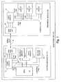
- an electronic unit 10in this embodiment a motor drive, includes a controller module 11 and a peripheral module 30, which in this embodiment are mounted on different circuit boards. In other embodiments, they could be located on one individual circuit board.
- the controller module 11has a microelectronic CPU 14 with address, data and control buses 15a, 16a and 17a, for transmitting signals to a logic circuit 13, to memories 18 and 19, to a chip select decoding circuit 20 and to a high speed serial-parallel data conversion circuit 21.
- the serial-parallel data conversion circuit 21communicates through a high speed serial data link 22 to the peripheral module 30.
- the memories 18, 19include a program memory 18 which stores program instructions for carrying out the operations of the CPU 14 and a data memory 19 for storing application data and temporary results.
- the peripheral module 30includes a logic circuit 31 and a high speed serial-parallel data conversion circuit 32 for communicating data on the high speed serial data link 22.
- the output from the serial-parallel data conversion circuit 32will be functionally the same address, data and control buses 15b, 16b and 17b that were present on the controller module 11, but at a greater distance from the CPU 14.
- the lines in these buses 15b, 16b and 17bwill connect to functional circuits on the peripheral module 30 which may include a peripheral CPU, however such a CPU will not function in any way in re-forming the address, data and control buses 15', 16' and 17' of the microelectronic CPU 14.
- Fig. 2shows the details of the logic circuits 13, 31 and the serial-parallel conversion circuits 21, 32 seen in Fig. 1 .
- the CPU data bus 16ais connected to the logic circuit 13.
- the data bus 16is serialized, transferred to the opposite side (inter-board or board to board) through the serial data link 22, and then reconverted to parallel data.
- the logic circuit 32re-forms the CPU data bus 16b.
- the CPU 14communicates to peripherals on external boards as if they are directly connected and physically located next to the CPU 14.
- the logic circuit 13more particularly includes a bus interface circuit 24a with transmit buffers and receive registers, a transaction/type control circuit 25a, bus control logic 26a and a wait state controller 27a.
- These circuits 25a-27areceive the read (RD), write (WR), chip select (CS) signals and generate wait state signals which form the CPU control bus 17.
- the serial-parallel data conversion circuit 21more particularly includes a LVDS (low voltage differential signaling) serial channel transmitter 28a, and a LVDS serial channel receiver 29a.
- the transmit datacomes into the circuit 28a as parallel data and is converted to serial data.
- the receive datacomes into the circuit 29a as serial data and is converted to parallel data.
- the serial-parallel data conversion circuit 21also includes a timing and control logic section 33a, which receives transaction sequencing and type signals from the transaction/type control circuit 25a and incorporates these in the serial data.
- This circuit 25aalso generates receive clock signal (Rec Clk 1) to help the timing of data being read by the CPU 14.
- the serial-parallel conversion circuit 32On the other side of the serial data link 22, the serial-parallel conversion circuit 32 has a LVDS (low voltage differential signaling) serial channel transmitter 28b, and a LVDS serial channel receiver 29b.
- the serial-parallel data conversion circuit 32also includes a timing and control logic section 33b, which extracts transaction sequencing and type signals from the serial data and passes these signals to a transaction type control circuit 25b which further controls read and write control signals in the control bus 17b.
- the serial-parallel conversion circuit 32includes a bus interface circuit 24b with transmit buffers and receive registers, a transaction/type control circuit 25b, bus control logic 26b and a wait state controller 27b similar to circuit 13.
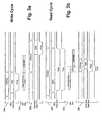
- Figs. 3a and 3bshow the timing of the data transfer in the circuit of Figs. 1 and 2 .
- Fig. 3aillustrates timing signals 34a for a typical CPU data bus in the write data transfer.
- the SerDes portion 35a in Fig. 3arepresents the signals being transmitted through the serial data link 22.
- the extended data bus portion 36ashows how the CPU bus signals are re-formed in buses 15b, 16b and 17b. It is to be noticed that the write cycle first takes place during the logic low active state of the write signal. During that time, the serial-parallel conversion circuit 21 generates control signals, places them in the write data and transmits the write data through the serial data link 22. After it is received and converted to parallel data by circuit 31, the data is finally written out to the extended data bus 16b as shown by signals 36a.
- the CPU cycle 34acan be completed prior to the peripheral module 30 having received the data 36a. This may have an advantage to allow the CPU 14 to execute the write transfer without any wait state requirements. Of course, the logic then requires a latch to hold the data until the serial-parallel circuit 21 has time to transfer the data. It is also important to realize that the transfer is after the CPU write cycle so some latency is noted.
- serial communications on the serial data link 22provide for continuous streaming of data.
- communication of data through the serial data link 22is not started and stopped.
- small two bits of additional transaction (Trans [1,0]) informationare embedded within the message data stream in the most significant byte (MSB) of address frame 60 as seen in Fig. 6 .
- MSBmost significant byte
- the transaction sequenceis simply 0, 1, 2, 3 and then restarts at 0 again so that each new transfer can be identified. Otherwise, data would be transferred and requested continuously without knowing when the data is complete and to complete the data transfer with the CPU (especially for a Read cycle). It is noted here that each frame of data in Fig.
- command informationcan be embedded into the message as part of the address.
- One bitis enough to determine whether the transaction is a write or a read from one peripheral board, but in this case two bits can be used to signal four possible transactions with additional boards in a multi-drop configuration seen in Fig. 7 .
- command informationsuch as Type information (see LSB address in Fig. 6 ) with the least significant byte (LSB) of address information
- the type of transfercan be synchronized with the reception of the address to determine whether a write (CPU output) or read (CPU input) transfer is being signaled.
- the low-level protocolprovides for embedding up to seven bits of error correction code (ECC 0-6) data in the 10-bit frames of information being transmitted over the serial data link 22.
- ECC 0-6error correction code
- the number of bits of error correction code neededdepends on the size of data transfer and seven bits is sufficient for transferring and validating 32 bits of data.
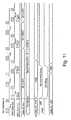
- Fig. 7illustrates a multi-drop (to two peripheral circuit boards) configuration.
- a second serial data channel(Ch. 2) can be added. This can allows for respective serial data channels between the controller board 11 and the peripheral boards 30a and 30b.
- the peripheral boards 30a and 30beach have their own serial interface and receive and transmit circuits 32a, 32b. In the write direction, address and data can be transferred at the same time, thus reducing the serial transport latency by half.
- the controller 11can communicate with different peripheral boards 30a and 30b using the same serial interface circuits assisted by two bi-directional serial data channels (Ch. 1, Ch. 2).
- Fig. 4shows the details of a logic circuit 13c and a high speed parallel-to-serial data conversion circuit 21 c for a multi-serial channel embodiment operating at 800MHz on each channel.
- the address, control and data buses 15c, 16c and 17cconnect to the logic circuit 13c, which is a field programmable gate array circuit (FPGA).
- FPGAfield programmable gate array circuit
- On the other side of the FPGA 13aare a plurality of serial-parallel conversion and serial communication circuits 41-44, the circuits 41, 42 for transmit channels 1-4 transmitting four bytes of data on four half-duplex serial output channels, and the circuits 43-44 for receive channels 1-4 for receiving four bytes of input data on four half-duplex serial input channels.
- the transmit portions of the four serial data channels 41, 42are used for sixteen bits of address data, and for sixteen bits of write address data, respectively.
- the receive portions of two serial data channels 43are used for sixteen bits of read address data.
- the receive portions 44 of serial data channels 3 and 4are used for a second sixteen bits of read address data for a total of thirty-two bits of read address data.
- the last two receive channels 44can be used for serial read streaming data or regular receive data. Because the CPU 14 in this example uses a 16-bit data bus, sending 32-bit data in four simultaneous transfers gets the data back but does not speed the read cycles of the CPU data bus 16a. After the first sixteen bits are received, the CPU 14 can continue the cycle. By the time the second cycle for the last sixteen bits is requested, the data is already received. If the data bus was 32 bits wide then implementing a 4-channel receive data would in fact improve the performance of the serial interface.
- the logic circuit 13, 13c for both Figs. 2 and 4is provided in one Altera Cyclone EP1C12 FPGA (Field Programmable Gate Array). although other specific commercial circuits could also be used.
- the logic circuit 13, 13cis responsible for coordinating the serial data interface activities between the main CPU 14 and the peripheral module 30c. The precise internal logic would vary according to which specific parallel-to-serial circuitry unit was chosen from a one of several suppliers, however, the functions described herein would still apply. The following are the functions performed for this logic circuit 13, 13c.
- the FPGA 13cincludes a CPU data bus interface portion 24c that provides a bi-directional tri-state interface to the main CPU 14 with a data bus width of 16 bits. It uses the typical complement of control signals which include Address bits A0 thru 15, Data bits D0 thru D15, read, write, CS (chip select), and Wait.
- the CPU data bus interface portion 24calso includes storage registers for storing transmit data and receive data, which is necessary to coordinate the discrete CPU data with the continuous data streaming of the serial-parallel data conversion circuit 21 a. Data registers are used for the temporary retention of this information until needed.
- the FPGA 13calso includes a transaction control section (not shown). Based upon the data transfer cycle being performed by the CPU 14, this logic determines and transfers the appropriate bit signals for establishing the Command Type (RD or WR) and the Data Sequence (most significant word, least significant word - 16 bits each). This information is stored with the address and data register latch and is transferred to the serial-parallel data conversion circuit 21c as timing requires.
- RD or WRCommand Type
- Data Sequencemost significant word, least significant word - 16 bits each
- the FPGA 13calso includes a bus control logic portion 25c that controls the state sequencing of operation of the serial-parallel data conversion circuit 21 c.
- the logicinterfaces with the Receive Clock signals (for determining when data is available) of the serial-parallel data conversion circuit 21 a and coordinating the transfer cycle that includes storing data in the registers, starting cycles based upon chip select activation, control of wait signal for holding off the CPU 14 and accumulating and evaluating error conditions.
- the data bus interface section 24calso includes an Error Checking and Correction (ECC) portion.
- ECCError Checking and Correction
- This logic blockwill perform the ECC generation, checking, and correction of the data transferred.
- the implementationcould be of several types depending on the integrity desired.
- the serial-parallel data conversion circuit 21 cperforms high speed bit rate clocking (Phase-locked loop), the serialization and transmitting of transmitting data, the de-serialization of receiving data, CDR (Clock Data Recovery, LVDS interfaces (Rx and Tx), and data encoding-decoding.
- This sectioninterfaces to the FPGA 13c.
- a 66.6666MHz clock 49drives the phase-locked loop that multiplies the frequency by 12 (12-bit encoding scheme) for a baud frequency of 800 MHz.
- the clock ratecan be stepped up to 3.2 Ghz.
- the parallel to serial converter sectionis a single chip device manufactured by Lattice Semiconductor, of Hillsboro, Oregon, as part number GDX2-128.
- This circuit 32dincludes the high speed bit rate clocking (PLL), the serialization of transmitting parallel data, de-serialization of receiving data, CDR (Clock Data Recovery, LVDS interfaces (Rx and Tx), and data encoding-decoding.
- This circuit 32dinterfaces to a peripheral module logic circuit 31 d provided by a second FPGA.
- a 66.6666MHz clock 49adrives the PLL that multiplies the frequency by 12 (12-bit encoding scheme) for a frequency of 800MHz.
- the clock ratecan be stepped up to 3.2 Ghz.
- the second serial-parallel converter circuit 32ais also a single chip device manufactured by Lattice Semiconductor as part number GDX2-128.
- the second FPGA 31dis provided in one Altera Cyclone EP1C12 FPGA (Field Programmable Gate Array), although other specific commercial circuits could also be used.
- the logic blockis responsible for coordinating the serial data interface activities between the serial channels and the peripheral module 30d. The precise internal logic would vary according to which specific parallel-to-serial circuitry unit was chosen from a one of several suppliers, however, the functions described herein would still apply.
- This logic blockis responsible for re-creating the timing and operational signals for the reproduced data bus on the remote end of the interface. The following are the functions performed for this logic block.
- the second FPGA 31dincludes a peripheral bus interface section 24d.
- This logicprovides a bi-directional tri-state interface to the peripherals connected to the data bus 16d.
- the re-generated data bus widthof thirty-two (32) bits. It uses the typical complement of control signals which include Address A0 thru 15, Data D0 thru D15, read, write, chip select, and wait.
- the second FPGA 31dincludes storage registers for storing transmit data and receive data. Since the data transfers to peripheral circuits would not be synchronized with the continuous data streaming of the parallel-serial conversion unit, data registers are used for the temporary retention of this information until data is available or transfer cycles are completed.
- the second FPGA 31dincludes a transaction control section (not shown) to determine the appropriate bit signals to be activated (RD or WR) and when the chip select outputs are active. This transaction information is received with the address and data frames and is transferred from the parallel-to-serial conversion circuit 32d as timing requires.
- the second FPGA 31dincludes a bus control section 25d. This portion of the logic controls the state sequencing of operation of the parallel-to-serial conversion circuit 32d.
- the logicinterfaces with the Receive Clock signals (for determining when data is available) of the parallel-to-serial conversion circuit and coordinating the transfer cycle that includes storing data in the registers, starting cycles based upon chip select activation, and monitoring of wait signal for generating return data sent back to the Host CPU.
- the second FPGA 31dincludes error code checking and correction (ECC) circuitry.
- ECCerror code checking and correction
- This logic blockwill perform the error code generation, checking, and correction of the data transferred.
- the controller and peripheral ECC circuitswould be required to check receive data and correct for errors as well as generate the ECC bits for transmitted data.
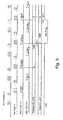
- Fig. 6illustrates the format of the serial data that is transferred in the write direction and the read direction from the CPU 14 to the peripheral module 12.
- a 10-bit/12-bit (10 bits of information/12 bits total) encoding/decoding formatis used to provide a start bit, a stop bit and ten bits of data per frame transfer.
- two bitscan be used for transaction control, type, ID and ECC bit data.
- Fig. 6shows six frames 60-65 for transmitting information as follows: most significant byte of address 60 (on Serial Data Channel 1), least significant byte of address 61 (on Serial Data Channel 2), most significant half of the first data word 62 (on Serial Data Channel 3), least significant half of the first data word 63 (on Serial Data Channel 4), most significant half of the second data word 64 (on Serial Data Channel 3), and the least significant half of the second data word 65 (serial channel 4).
- Fig. 6the placement of the bits within the frame are shown. It is important to note that when transferring a serial data stream, that changing bits as often as possible aids in the synchronization of the data streams between serial-parallel conversion units. That is why the selected embedded bits are in the middle of the 10-bit data frame.
- the embedded bitscan be defined to maximize the bit transitions.
- the most-significant-byte-of-address frame 60includes the two bits with a transaction number from 00 to 03 which identifies this frame as new from the frame previously sent through that channel. Data is continually being sent whether or not any new information is being transferred or requested.
- the two bitsare count from 00 to 03 and the turn over and repeat. If necessary, the same 01 and 10 pattern can be used. Every other transaction would be repeated with the same number. This specific design is utilizing a repeating one of four count.
- the least-significant-byte-of-address frame 61includes the two bits with a type number from 00 to 03 in which a read type is 01 and a write type as 10. This allows a transition to maximize the synch of the serial to parallel circuits.
- a further read typecan be defined as 00 and a further write type can be defined as 11.
- Fig. 6shows the following four frames 66-69 for reading 32 bits of data on Channels 1 and 2 in response to address frames 60 and 61: most significant byte of first word of read data 66, least significant byte of first word of read data 67, most significant byte of second word of read data word 68, least significant byte of second word of read data word 69. All of these are received on read channels 1 and 2. It is also possible to receive a second 32-bit word of read data on read channels 3-4.
- information that is embedded in bits 04 and 05is the data identifier (ID) and the ECC bits.
- IDthe data identifier
- ECC bitsthe ECC bits. This enables the remote units to identify the proper order of data and the change of frame to indicate this is new from the previous data stream transfer.
- the data width being transferredis 32 bits.
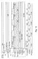
- Figs. 8-11illustrate the timing sequences for a Write Data Transfer and a Read Data Transfer between the controller CPU 14 and the peripheral module 30d.
- the write cycleis simpler and less intrusive to the CPU performance than the read cycle.
- the CPUis required to transfer a 32-bit word (MSW 16-bit word and LSW 16-bit word in the FPGA section) to the parallel-serial interface.
- the CPU address A0-A15, data D0-D15, chip select (/CS) and write (/WR) signals, as well as the external synchronizing clock signalsare seen in the top portion of Fig. 8 .
- the next portionshows the signals generated through by the FPGA including alternating valid time frames for address and data, the generation of signals for a write transaction, including the generation of a new sequence number and the write data.
- the bottom two graphs in Fig. 8show the times when the address and data are generated on the serial data link 22 by the serial-parallel conversion circuit 21d.
- the first four lines of Fig. 9shows the timing of the signals processed by the second serial-parallel conversion circuit 32d, and finally the bottom three lines show the address and data being signaled on the extended buses 15d, 16d.
- data streamingcontinues to be received or sent from/to the controller module 11.
- the sequence numberis changed to that the peripheral module 30d can detect that this is a new transaction and not the same data that was previously sent.
- Another approach to identifying datais the idle packet approach. This could be used in alternative embodiments, but is not preferred, because it might introduce latency into the data transfer.
- the ID bitis used to specify whether the received data is the most significant 16 bits or the least significant 16 bits.
- Fig. 10the CPU signals for a read cycle are shown including address A0-A15, data D0-D15, chip select (/CS) and read (/RD) signals, as well as the external synchronizing clock signals are seen in the top portion of Fig. 10 .
- the next portionshows the signals generated by the FPGA including alternating valid time frames for address and data, the generation of signals for a read transaction, including the generation of a new sequence number and a wait (WAIT) signal.
- the bottom two graphs in Fig. 10show the times when the address and data are generated on the serial data link 22 by the serial-parallel conversion circuit 21 c.
- the first four lines of Fig. 11show the timing of the signals processed by the second serial-parallel conversion circuit 32d to read data, and finally the bottom three lines show the address, the read data and the wait signal being signaled on the extended buses 15d, 16d, 17d.
- the addressis received and a receive clock signal is generated to the logic to save the address. From this data, the logic on the peripheral module 30d will determine whether, the data is write data or read data. Since it is read data, a Read pulse is enabled. After the Wait signal from the remote peripheral is released (data is ready), the data is latched into the FPGA's transmit buffer and the Read signal is de-activated. At the next serial link transfer interval, the first 16 bits (MS) are transferred. Then the second 16 bits (LS) is transferred.
- the Wait signalis de-activated and the first read cycle is concluded.
- the CPUthen repeats the read cycle for the last 16 bits for which the data is available and no Wait signal would be necessary to activate. This is of course unless the data bus bandwidth exceeds the serial link transfer time.
- data streamingcontinues to be received or sent from/to the controller 11c.
- the sequence numberis changed to that the peripheral module can detect that this is a new transaction and not the same data that was previously sent.
- the ID bitis used to specify whether the received data is the most significant 16 bits or the least significant 16 bits.
- the buses 15c, 16c, 17c of the CPU 14can be extended from as few as three inches to up to forty inches without incurring the data latency problems of parallel data buses.
- the principlecan be applied across multiple circuit boards on within one large circuit board. No CPU is required on the peripheral module to help reconstruct the buses.
Landscapes
- Engineering & Computer Science (AREA)
- Theoretical Computer Science (AREA)
- Physics & Mathematics (AREA)
- General Engineering & Computer Science (AREA)
- General Physics & Mathematics (AREA)
- Information Transfer Systems (AREA)
- Bus Control (AREA)
- Communication Control (AREA)
- Time-Division Multiplex Systems (AREA)
Description
- The field of the invention is electronic and computer equipment of type mounted on circuit boards and disposed on a chassis or in a housing, and a specific embodiment is related to the field of factory automation and motor controls.
- In factory automation and other applications requiring computerized equipment motors, the electronics are supported on circuit boards and mounted to a chassis or in a housing. The circuit boards may have edge connectors that are received in corresponding edge connectors mounted on a backplane motherboard. Or, as seen in personal computer equipment the circuitry may be connected with ribbon cable. Where units are some distance apart, cables or twisted pairs of wires or wireless technologies can be used to transmit data through a serial data communication channel according to serial data protocols.
- The present invention is concerned with information buses that extend across a physical medium either on a given board or between boards. In this context, the "information" category may be defined as including subcategories of more specific information, such as address information, data information or control information. Today, information bus widths are increasing from 32 bits to 64 bits and even to 128 bits. In parallel signal paths running at high speed, there is a problem concerning "data latency," where not all of the signals arrives at the destination within a time window defined for capture and processing.
- In electrically noisy environments, data latency can be a problem for buses operating at speeds as low as 20 MHz. As the speed of microelectronic CPU's has increased to 500 MHz and even greater than 1 GHz, the transport of data and densities across connectors can cause severe problems in data latency and result in cost disadvantages. Data transfer at these speeds can have the effect of limiting bus lengths to a few inches, which limits the circuitry that can communicate on such buses.
- Most serial data interface implementations require protocols, which are organizations of data into strings of defined bytes that can be sorted out and identified at the receiving end. Many protocol standards and specifications are provided for use today for serial communications. Some examples are Rapid I/O, USB, Firewire and others.
- These protocols will contain overhead in the form of identification data, command data, error detection data, and other information. The true performance of the serial channel is reduced depending on the overhead required by the protocol. Two characteristics of a serial channel called bit rate and bandwidth provide a measure of performance. The bit rate is the clock rate of the data stream which contains all frames of information including the substantive application data. The bandwidth is the data transfer speed that reflects how much of this data is transported in an interval of time. The frames of information that there are in addition to the substantive application data represent overhead in the serial data stream. Due to this overhead, the data bandwidth never reaches the serial bit rate. For example; a message with four (4) bytes of application data may require four (4) additional bytes of information such as address, commands and data checking (validation). The total is eight (8) bytes and assuming an 8 Mb serial data rate, the maximum transfer rate would be 1 million 8-byte messages per second or a 4Mb data bandwidth. Without the extra information, the bandwidth would be 8Mb. In this case the bandwidth is 50% of the serial bit rate.
- With the present invention, the bandwidth is increased to 67% of the serial bit rate.
WO 01/18989 A WO 01/18654 A - Avery James M: "Infiniband to PCI Bridge TCA" WGS VLSI ENGINEERING, 9 May 2000 (2000-05-09), relates to requirements for an Infiniband to PCI target channel adapter which serves as a remote bridge device for PCI adapters and controllers.
US20011044862 relates to a technique for serializing a parallel peripheral bus within a microcontroller. The technique is implemented by converting the parallel data, address, and control information on the parallel peripheral bus to a serial data stream. The serial data stream is then transmitted to an external device. It is also described to receive a serial data stream from an external device and converting the serial data stream to parallel data, address, and control information. The parallel information is then transmitted to the embedded system on the parallel peripheral bus.- It is then the object of the present invention to provide an improved method and circuit for receiving parallel address, data and control bus information from a CPU and transferring the information to a destination and presenting the data as reconstituted parallel information for utilization by peripheral devices by utilizing parallel to serial and serial to parallel conversion.
- This object is solved by the subject matter of the independent claims.
- Preferred embodiments are defined in the dependent claims.
- The invention relates to a method and a circuit for converting parallel information buses within circuit boards to serial data buses and then re-forming the parallel data, using a low-level serial data protocol without overhead frames. With this approach, bus distances can be increased for high speeds from three up to forty inches. Also, the information bandwidth will be increased.
- It is a further aspect of the invention that larger scale parallel data buses can be converted to serial data by subdividing the buses into a plurality of serial data channels. The invention utilizes high speed serial data circuitry along with custom logic circuits for converting the information on the parallel buses to serial data on the sending end and for re-converting the information to the original parallel data form on the receiving end. The invention can be applied to bi-directional transfer of information and to the connection of a controller circuit board to a plurality of peripheral boards.
- In one embodiment, the method of the invention is practiced by receiving the parallel address, data and control bus information near the microelectronic CPU and converting that information to serial data information in a plurality of serial data streams, and transmitting the serial data streams to circuitry near the destination and converting the serial data streams to parallel address, data and control bus information to reconstitute the microelectronic CPU information buses as peripheral information buses. The serial data streams are transparent to the peripheral devices which may be connected to the peripheral information buses. Also, the converting of said information to the serial data streams to parallel address, data and control bus information is carried out without assistance by a second CPU.
- The circuitry of the invention includes first storage circuits for receiving the parallel address, data and control bus information near the microelectronic CPU, first conversion circuits for converting the information to serial data information in a plurality of serial data streams and transmitting the serial data streams to circuitry near the destination, second conversion circuits for converting the serial data streams to parallel address, data and control bus information, and address, data and control bus information to reconstitute the microelectronic CPU information buses or peripheral information buses.
- Various objects and advantages of the invention will be apparent from the description that follows and from the drawings which illustrate embodiments of the invention, and which are incorporated herein by reference.
Fig. 1 is a block diagram illustrating one preferred embodiment of a circuit for practicing the present invention;Fig. 2 is a more detailed block diagram of the circuits seen inFig. 1 ;Figs. 3a and 3b are generalized timing diagrams for reading and writing data in the embodiments ofFigs. 1 and2 ;Figs. 4 and5 are more detailed block diagrams of circuits seenFig. 1 for a thirty-two bit data bus embodiment;Fig. 6 is a map diagram of the serial data transferred in both directions inFigs. 1 ,2 ,4 and5 ;Fig. 7 shows the invention applied to a multi-drop configuration with two peripheral circuit boards; andFigs. 8-11 are more detailed timing diagrams of the information transfer within the circuits ofFigs. 4 and5 .- Referring to
Fig. 1 , anelectronic unit 10, in this embodiment a motor drive, includes acontroller module 11 and aperipheral module 30, which in this embodiment are mounted on different circuit boards. In other embodiments, they could be located on one individual circuit board. - The
controller module 11 has amicroelectronic CPU 14 with address, data andcontrol buses logic circuit 13, tomemories select decoding circuit 20 and to a high speed serial-paralleldata conversion circuit 21. The serial-paralleldata conversion circuit 21 communicates through a high speed serial data link 22 to theperipheral module 30. Thememories program memory 18 which stores program instructions for carrying out the operations of theCPU 14 and adata memory 19 for storing application data and temporary results. - The
peripheral module 30 includes alogic circuit 31 and a high speed serial-paralleldata conversion circuit 32 for communicating data on the high speedserial data link 22. The output from the serial-paralleldata conversion circuit 32 will be functionally the same address, data andcontrol buses controller module 11, but at a greater distance from theCPU 14. The lines in thesebuses peripheral module 30 which may include a peripheral CPU, however such a CPU will not function in any way in re-forming the address, data and control buses 15', 16' and 17' of themicroelectronic CPU 14. Fig. 2 shows the details of thelogic circuits parallel conversion circuits Fig. 1 . TheCPU data bus 16a is connected to thelogic circuit 13. Thedata bus 16 is serialized, transferred to the opposite side (inter-board or board to board) through theserial data link 22, and then reconverted to parallel data. Thelogic circuit 32 re-forms theCPU data bus 16b. As a result, theCPU 14 communicates to peripherals on external boards as if they are directly connected and physically located next to theCPU 14.- As seen in
Fig. 2 , thelogic circuit 13 more particularly includes abus interface circuit 24a with transmit buffers and receive registers, a transaction/type control circuit 25a,bus control logic 26a and await state controller 27a. Thesecircuits 25a-27a receive the read (RD), write (WR), chip select (CS) signals and generate wait state signals which form the CPU control bus 17. - The serial-parallel
data conversion circuit 21 more particularly includes a LVDS (low voltage differential signaling)serial channel transmitter 28a, and a LVDSserial channel receiver 29a. The transmit data comes into thecircuit 28a as parallel data and is converted to serial data. The receive data comes into thecircuit 29a as serial data and is converted to parallel data. The serial-paralleldata conversion circuit 21 also includes a timing and controllogic section 33a, which receives transaction sequencing and type signals from the transaction/type control circuit 25a and incorporates these in the serial data. Thiscircuit 25a also generates receive clock signal (Rec Clk 1) to help the timing of data being read by theCPU 14. - On the other side of the
serial data link 22, the serial-parallel conversion circuit 32 has a LVDS (low voltage differential signaling)serial channel transmitter 28b, and a LVDSserial channel receiver 29b. The serial-paralleldata conversion circuit 32 also includes a timing and controllogic section 33b, which extracts transaction sequencing and type signals from the serial data and passes these signals to a transactiontype control circuit 25b which further controls read and write control signals in thecontrol bus 17b. The serial-parallel conversion circuit 32 includes abus interface circuit 24b with transmit buffers and receive registers, a transaction/type control circuit 25b,bus control logic 26b and await state controller 27b similar tocircuit 13. Figs. 3a and 3b show the timing of the data transfer in the circuit ofFigs. 1 and2 .Fig. 3a illustrates timing signals 34a for a typical CPU data bus in the write data transfer. TheSerDes portion 35a inFig. 3a represents the signals being transmitted through theserial data link 22. The extendeddata bus portion 36a shows how the CPU bus signals are re-formed inbuses parallel conversion circuit 21 generates control signals, places them in the write data and transmits the write data through theserial data link 22. After it is received and converted to parallel data bycircuit 31, the data is finally written out to the extendeddata bus 16b as shown bysignals 36a.- As seen in
Fig. 3a , for a write transfer, theCPU cycle 34a can be completed prior to theperipheral module 30 having received thedata 36a. This may have an advantage to allow theCPU 14 to execute the write transfer without any wait state requirements. Of course, the logic then requires a latch to hold the data until the serial-parallel circuit 21 has time to transfer the data. It is also important to realize that the transfer is after the CPU write cycle so some latency is noted. - As seen in
Fig. 3b , there aresignals 34b on the CPU data bus, signals 35b in the serial-parallel (Serdes) portions of themodules extended buses CPU data bus 16 must wait for the data to be received from theperipheral module 30. This requires a wait signal to be utilized for this type of transfer. The delay will include serial transport time and the physical wait state delay of the peripheral being addressed. - The serial communications on the
serial data link 22 provide for continuous streaming of data. In order to remain in synchronization with a peripheral device, communication of data through theserial data link 22 is not started and stopped. To signal when a new transaction is started or completed, small two bits of additional transaction (Trans [1,0]) information are embedded within the message data stream in the most significant byte (MSB) ofaddress frame 60 as seen inFig. 6 . The transaction sequence is simply 0, 1, 2, 3 and then restarts at 0 again so that each new transfer can be identified. Otherwise, data would be transferred and requested continuously without knowing when the data is complete and to complete the data transfer with the CPU (especially for a Read cycle). It is noted here that each frame of data inFig. 6 includes ten (10) bits of information (plus a start and stop bit that are not shown). After subtracting two bits of control data, the result is eight bits of information from the CPU buses, so reference to MSB (most significant byte) and LSB (least significant byte) identifies these frames by according to the sequence in transferring 16-bit words of information. - With the low level of protocol information (2 bits per frame) seen in
Fig. 6 , command information can be embedded into the message as part of the address. One bit is enough to determine whether the transaction is a write or a read from one peripheral board, but in this case two bits can be used to signal four possible transactions with additional boards in a multi-drop configuration seen inFig. 7 . - By embedding command information, such as Type information (see LSB address in
Fig. 6 ) with the least significant byte (LSB) of address information, the type of transfer can be synchronized with the reception of the address to determine whether a write (CPU output) or read (CPU input) transfer is being signaled. - As seen further in
Fig. 6 , the low-level protocol provides for embedding up to seven bits of error correction code (ECC 0-6) data in the 10-bit frames of information being transmitted over theserial data link 22. The number of bits of error correction code needed depends on the size of data transfer and seven bits is sufficient for transferring and validating 32 bits of data. Fig. 7 illustrates a multi-drop (to two peripheral circuit boards) configuration. As an alternative to increasing the serial data rate to improve performance, a second serial data channel (Ch. 2) can be added. This can allows for respective serial data channels between thecontroller board 11 and theperipheral boards peripheral boards circuits controller 11 can communicate with differentperipheral boards Fig. 4 shows the details of alogic circuit 13c and a high speed parallel-to-serialdata conversion circuit 21 c for a multi-serial channel embodiment operating at 800MHz on each channel. The address, control anddata buses logic circuit 13c, which is a field programmable gate array circuit (FPGA). On the other side of the FPGA 13a are a plurality of serial-parallel conversion and serial communication circuits 41-44, thecircuits - The transmit portions of the four
serial data channels serial data channels 43 are used for sixteen bits of read address data. The receiveportions 44 ofserial data channels - The last two receive
channels 44 can be used for serial read streaming data or regular receive data. Because theCPU 14 in this example uses a 16-bit data bus, sending 32-bit data in four simultaneous transfers gets the data back but does not speed the read cycles of theCPU data bus 16a. After the first sixteen bits are received, theCPU 14 can continue the cycle. By the time the second cycle for the last sixteen bits is requested, the data is already received. If the data bus was 32 bits wide then implementing a 4-channel receive data would in fact improve the performance of the serial interface. - The
logic circuit Figs. 2 and4 is provided in one Altera Cyclone EP1C12 FPGA (Field Programmable Gate Array). although other specific commercial circuits could also be used. Thelogic circuit main CPU 14 and the peripheral module 30c. The precise internal logic would vary according to which specific parallel-to-serial circuitry unit was chosen from a one of several suppliers, however, the functions described herein would still apply. The following are the functions performed for thislogic circuit - The
FPGA 13c includes a CPU databus interface portion 24c that provides a bi-directional tri-state interface to themain CPU 14 with a data bus width of 16 bits. It uses the typical complement of control signals which include Address bits A0 thru 15, Data bits D0 thru D15, read, write, CS (chip select), and Wait. - The CPU data
bus interface portion 24c also includes storage registers for storing transmit data and receive data, which is necessary to coordinate the discrete CPU data with the continuous data streaming of the serial-parallel data conversion circuit 21 a. Data registers are used for the temporary retention of this information until needed. - The
FPGA 13c also includes a transaction control section (not shown). Based upon the data transfer cycle being performed by theCPU 14, this logic determines and transfers the appropriate bit signals for establishing the Command Type (RD or WR) and the Data Sequence (most significant word, least significant word - 16 bits each). This information is stored with the address and data register latch and is transferred to the serial-paralleldata conversion circuit 21c as timing requires. - The
FPGA 13c also includes a bus control logic portion 25c that controls the state sequencing of operation of the serial-paralleldata conversion circuit 21 c. The logic interfaces with the Receive Clock signals (for determining when data is available) of the serial-parallel data conversion circuit 21 a and coordinating the transfer cycle that includes storing data in the registers, starting cycles based upon chip select activation, control of wait signal for holding off theCPU 14 and accumulating and evaluating error conditions. - The data
bus interface section 24c also includes an Error Checking and Correction (ECC) portion. This is an optional feature. This logic block will perform the ECC generation, checking, and correction of the data transferred. The implementation could be of several types depending on the integrity desired. The present implementation includes a modified Hamming Code (distance = 4) to allow SECDED (single error correction double error detection). This implementation will allow good reliability yet reduce the amount of logic and delay time associated with it. - The serial-parallel
data conversion circuit 21 c performs high speed bit rate clocking (Phase-locked loop), the serialization and transmitting of transmitting data, the de-serialization of receiving data, CDR (Clock Data Recovery, LVDS interfaces (Rx and Tx), and data encoding-decoding. This section interfaces to theFPGA 13c. In this application, a 66.6666MHz clock 49 drives the phase-locked loop that multiplies the frequency by 12 (12-bit encoding scheme) for a baud frequency of 800 MHz. In other embodiments, the clock rate can be stepped up to 3.2 Ghz. The parallel to serial converter section is a single chip device manufactured by Lattice Semiconductor, of Hillsboro, Oregon, as part number GDX2-128. - Since the clock data recovery portion of the serial-parallel
data conversion circuit 21 c may not adequately keep synchronization of the data stream in this environment, a separate clock and LVDS clock driver was added to this block to insure synchronous operation. This required another LVDS channel to be transported across the interface. This may be removed in some embodiments. - On the
peripheral module 30d (Fig. 5 ) there is a second serial-parallel converter circuit 32d. Thiscircuit 32d includes the high speed bit rate clocking (PLL), the serialization of transmitting parallel data, de-serialization of receiving data, CDR (Clock Data Recovery, LVDS interfaces (Rx and Tx), and data encoding-decoding. Thiscircuit 32d interfaces to a peripheralmodule logic circuit 31 d provided by a second FPGA. In this application, a 66.6666MHz clock 49a drives the PLL that multiplies the frequency by 12 (12-bit encoding scheme) for a frequency of 800MHz. In other embodiments, the clock rate can be stepped up to 3.2 Ghz. The second serial-parallel converter circuit 32a is also a single chip device manufactured by Lattice Semiconductor as part number GDX2-128. - The
second FPGA 31d is provided in one Altera Cyclone EP1C12 FPGA (Field Programmable Gate Array), although other specific commercial circuits could also be used. The logic block is responsible for coordinating the serial data interface activities between the serial channels and theperipheral module 30d. The precise internal logic would vary according to which specific parallel-to-serial circuitry unit was chosen from a one of several suppliers, however, the functions described herein would still apply. This logic block is responsible for re-creating the timing and operational signals for the reproduced data bus on the remote end of the interface. The following are the functions performed for this logic block. - The
second FPGA 31d includes a peripheralbus interface section 24d. This logic provides a bi-directional tri-state interface to the peripherals connected to thedata bus 16d. The re-generated data bus width of thirty-two (32) bits. It uses the typical complement of control signals which include Address A0 thru 15, Data D0 thru D15, read, write, chip select, and wait. - The
second FPGA 31d includes storage registers for storing transmit data and receive data. Since the data transfers to peripheral circuits would not be synchronized with the continuous data streaming of the parallel-serial conversion unit, data registers are used for the temporary retention of this information until data is available or transfer cycles are completed. - The
second FPGA 31d includes a transaction control section (not shown) to determine the appropriate bit signals to be activated (RD or WR) and when the chip select outputs are active. This transaction information is received with the address and data frames and is transferred from the parallel-to-serial conversion circuit 32d as timing requires. - The
second FPGA 31d includes abus control section 25d. This portion of the logic controls the state sequencing of operation of the parallel-to-serial conversion circuit 32d. The logic interfaces with the Receive Clock signals (for determining when data is available) of the parallel-to-serial conversion circuit and coordinating the transfer cycle that includes storing data in the registers, starting cycles based upon chip select activation, and monitoring of wait signal for generating return data sent back to the Host CPU. - The
second FPGA 31d includes error code checking and correction (ECC) circuitry. This logic block will perform the error code generation, checking, and correction of the data transferred. The present implementation includes a modified Hamming Code (distance = 4) to allow SECDED (single error correction double error detection). This implementation will allow good reliability yet reduce the amount of logic and delay time associated with it. The controller and peripheral ECC circuits would be required to check receive data and correct for errors as well as generate the ECC bits for transmitted data. Fig. 6 illustrates the format of the serial data that is transferred in the write direction and the read direction from theCPU 14 to theperipheral module 12. In the present embodiments, a 10-bit/12-bit (10 bits of information/12 bits total) encoding/decoding format is used to provide a start bit, a stop bit and ten bits of data per frame transfer. For each ten bits of data, two bits can be used for transaction control, type, ID and ECC bit data.Fig. 6 shows six frames 60-65 for transmitting information as follows: most significant byte of address 60 (on Serial Data Channel 1), least significant byte of address 61 (on Serial Data Channel 2), most significant half of the first data word 62 (on Serial Data Channel 3), least significant half of the first data word 63 (on Serial Data Channel 4), most significant half of the second data word 64 (on Serial Data Channel 3), and the least significant half of the second data word 65 (serial channel 4).- In
Fig. 6 , the placement of the bits within the frame are shown. It is important to note that when transferring a serial data stream, that changing bits as often as possible aids in the synchronization of the data streams between serial-parallel conversion units. That is why the selected embedded bits are in the middle of the 10-bit data frame. The embedded bits can be defined to maximize the bit transitions. - The most-significant-byte-of-
address frame 60 includes the two bits with a transaction number from 00 to 03 which identifies this frame as new from the frame previously sent through that channel. Data is continually being sent whether or not any new information is being transferred or requested. - For the transaction number, the two bits are count from 00 to 03 and the turn over and repeat. If necessary, the same 01 and 10 pattern can be used. Every other transaction would be repeated with the same number. This specific design is utilizing a repeating one of four count.
- The least-significant-byte-of-
address frame 61 includes the two bits with a type number from 00 to 03 in which a read type is 01 and a write type as 10. This allows a transition to maximize the synch of the serial to parallel circuits. In a multi-drop configuration, when the a further read type can be defined as 00 and a further write type can be defined as 11. - The bottom portion of
Fig. 6 shows the following four frames 66-69 for reading 32 bits of data onChannels frames 60 and 61: most significant byte of first word ofread data 66, least significant byte of first word ofread data 67, most significant byte of second word ofread data word 68, least significant byte of second word ofread data word 69. All of these are received onread channels - In the read data frame(s), information that is embedded in
bits Figs. 8-11 illustrate the timing sequences for a Write Data Transfer and a Read Data Transfer between thecontroller CPU 14 and theperipheral module 30d.- The write cycle is simpler and less intrusive to the CPU performance than the read cycle. The CPU is required to transfer a 32-bit word (MSW 16-bit word and LSW 16-bit word in the FPGA section) to the parallel-serial interface. The CPU address A0-A15, data D0-D15, chip select (/CS) and write (/WR) signals, as well as the external synchronizing clock signals are seen in the top portion of
Fig. 8 . The next portion shows the signals generated through by the FPGA including alternating valid time frames for address and data, the generation of signals for a write transaction, including the generation of a new sequence number and the write data. The bottom two graphs inFig. 8 show the times when the address and data are generated on theserial data link 22 by the serial-parallel conversion circuit 21d. - The first four lines of
Fig. 9 shows the timing of the signals processed by the second serial-parallel conversion circuit 32d, and finally the bottom three lines show the address and data being signaled on theextended buses - During the transfer process, data streaming continues to be received or sent from/to the
controller module 11. When a new Write cycle is activated, the sequence number is changed to that theperipheral module 30d can detect that this is a new transaction and not the same data that was previously sent. Another approach to identifying data is the idle packet approach. This could be used in alternative embodiments, but is not preferred, because it might introduce latency into the data transfer. During the data transfer portion of the data streaming in the preferred embodiment, the ID bit is used to specify whether the received data is the most significant 16 bits or the least significant 16 bits. - In
Fig. 10 , the CPU signals for a read cycle are shown including address A0-A15, data D0-D15, chip select (/CS) and read (/RD) signals, as well as the external synchronizing clock signals are seen in the top portion ofFig. 10 . The next portion shows the signals generated by the FPGA including alternating valid time frames for address and data, the generation of signals for a read transaction, including the generation of a new sequence number and a wait (WAIT) signal. The bottom two graphs inFig. 10 show the times when the address and data are generated on theserial data link 22 by the serial-parallel conversion circuit 21 c. - The first four lines of
Fig. 11 show the timing of the signals processed by the second serial-parallel conversion circuit 32d to read data, and finally the bottom three lines show the address, the read data and the wait signal being signaled on theextended buses - On the
peripheral module 30d, the address is received and a receive clock signal is generated to the logic to save the address. From this data, the logic on theperipheral module 30d will determine whether, the data is write data or read data. Since it is read data, a Read pulse is enabled. After the Wait signal from the remote peripheral is released (data is ready), the data is latched into the FPGA's transmit buffer and the Read signal is de-activated. At the next serial link transfer interval, the first 16 bits (MS) are transferred. Then the second 16 bits (LS) is transferred. - When the
controller 11 receives all the data, the Wait signal is de-activated and the first read cycle is concluded. The CPU then repeats the read cycle for the last 16 bits for which the data is available and no Wait signal would be necessary to activate. This is of course unless the data bus bandwidth exceeds the serial link transfer time. - During the transfer process, data streaming continues to be received or sent from/to the
controller 11c. When a new Read cycle is activated, the sequence number is changed to that the peripheral module can detect that this is a new transaction and not the same data that was previously sent. During the data transfer portion of the data streaming, the ID bit is used to specify whether the received data is the most significant 16 bits or the least significant 16 bits. - With the present invention, the
buses CPU 14 can be extended from as few as three inches to up to forty inches without incurring the data latency problems of parallel data buses. The principle can be applied across multiple circuit boards on within one large circuit board. No CPU is required on the peripheral module to help reconstruct the buses.
Claims (22)
- A method for receiving parallel address (15a), data (16a) and control (17a) bus information from a CPU (14) and transferring the CPU information to a destination (30) and presenting the data as reconstituted parallel address (15b), data (16b) and control (17b) bus information for utilization by peripheral devices, the method comprising:receiving the CPU information (34a, 34b) including parallel address (15a), data (16a) and control (17a) bus information proximate the CPU (14), the method beingcharacterized by the steps of: converting the CPU information to serial data information (35a, 35b), including converting the information to a plurality of serial data streams and embedding read/write type and transaction number information in the serial data streamstransmitting the serial data information (35a, 35b) as a continuous data stream to peripheral circuits near the destination, including transmitting the serial data streams as separate serial data streams to the peripheral circuits; andconverting the serial data Information (35a, 35b) to parallel address (15b), data (16b) and control (17b) bus information to reconstitute the CPU information (34a, 34b) as peripheral information (36a, 36b), including converting the serial data streams to parallel bus information, comprising recovering the read/write type and transaction number information to assist in identifying the address and data information received in the serial data streams,wherein the step of converting the serial data information to reconstitute the CPU information is carried out without assistance by a second CPU on the peripheral information buses.
- The method of claim 1 wherein the serial data information is transparent to the peripheral devices.
- The method of claim 1, further comprising:decoding the serial data streams near the destination.
- The method of claim 1, further comprising:including error checking information in the serial data streams; andrecovering the error checking information near the destination for verifying the data before said information is made available to the peripheral circuits.
- The method of claim 1, wherein
the parallel information received from the CPU includes at least sixteen parallel bits of information and the parallel information presented to the peripheral devices comprises at least thirty-two parallel bits of information. - The method of claim 1, wherein the step of converting the serial data streams to parallel address, data and control bus information is performed without the assistance of any CPU at the destination.
- The method of claim 1, wherein the transmission frequency and the distance over which the transmission occurs between the CPU and the destination is such that the period required for transmission of each bit of series data may be greater than the transmission frequency.
- The method of claim 7, wherein the serial transmission rate is at least 800 Mbaud.
- The method of claim 8 wherein the transmission rate is at least 3.2 Gbaud.
- The method of claim 7 wherein the distance over which the data is transmitted is at least three inches.
- The method of claim 10 wherein the distance over which the data is transmitted is at least forty inches.
- The method of claim 1 wherein the transmission of serial data streams to the destination is synchronized by a transfer clock.
- The method of claim 1, wherein when data is received near the destination, receive clock signals are generated to transfer the data to latches for presentation to the peripheral devices.
- The method of claim 1, wherein converting the information to serial data information in a plurality of serial data streams is performed using a 12-bit encoding scheme,
- The method of claim 1, wherein the control bus signals comprise read, write, chip select and wait state signals.
- The method of claim 1 wherein the step of converting the serial data information to parallel address, data and control information is performed by a hardwired logic circuit without the assistance of any CPU at the destination.
- A circuit for receiving parallel address, data and control bus information from a CPU (14), transferring the information to a destination (30) and presenting the data as parallel address, data and control bus information for utilization by peripheral devices, the circuit comprising:first storage circuits (13) for receiving the parallel address (15a), data (16a) and control (17a) bus information from the CPU;said circuit beingcharacterized byfirst conversion circuits (21) for converting the information to a plurality of serial data streams (35a, 35b) and for transmitting the separate streams to the circuitry near the destination;a first control circuit for controlling the first conversion circuits to include read/write type and transaction number information in the serial data streams;second conversion circuits (32) for converting the serial data streams to reconstituted parallel address, data and control bus information, wherein the second conversion circuits convert without assistance from a second CPU;a second control circuit for interfacing with the second conversion circuits for recovering the read/write type and transaction number information to assist in identifying the address and data information received in the serial data streams; andsecond storage circuits (31) for holding the reconstituted parallel address (15b), data (16b) and control (17b) bus information to reconstitute the parallel information provided by the CPU.
- The circuit of claim 17 wherein the serial data information is transparent to the peripheral devices.
- The circuit of claim 17, the second control circuit further adapted for decoding the serial data streams near the destination.
- The circuit of claim 17, wherein the step of converting the serial data streams to parallel address, data and control bus information is performed by a hardwired logic circuit without the assistance of any CPU at the destination.
- The circuit of claim 17, wherein the transmission frequency and the distance over which the transmission occurs between the first and second conversion circuits is such that the period required for transmission of each bit of series data may be greater than the transmission frequency.
- The circuit of claim 17, further comprising a clock circuit that transmits clock signals to the second logic circuit for synchronizing the transmission of serial data streams to the destination.
Applications Claiming Priority (2)
| Application Number | Priority Date | Filing Date | Title |
|---|---|---|---|
| US11/011,964US7243173B2 (en) | 2004-12-14 | 2004-12-14 | Low protocol, high speed serial transfer for intra-board or inter-board data communication |
| PCT/US2005/045076WO2006065817A2 (en) | 2004-12-14 | 2005-12-13 | Low protocol, high speed serial transfer for intra-board or inter-board data communication |
Publications (2)
| Publication Number | Publication Date |
|---|---|
| EP1825382A2 EP1825382A2 (en) | 2007-08-29 |
| EP1825382B1true EP1825382B1 (en) | 2013-06-19 |
Family
ID=36386864
Family Applications (1)
| Application Number | Title | Priority Date | Filing Date |
|---|---|---|---|
| EP05853892.7ANot-in-forceEP1825382B1 (en) | 2004-12-14 | 2005-12-13 | Low protocol, high speed serial transfer for intra-board or inter-board data communication |
Country Status (3)
| Country | Link |
|---|---|
| US (1) | US7243173B2 (en) |
| EP (1) | EP1825382B1 (en) |
| WO (1) | WO2006065817A2 (en) |
Families Citing this family (27)
| Publication number | Priority date | Publication date | Assignee | Title |
|---|---|---|---|---|
| US6643777B1 (en)* | 1999-05-14 | 2003-11-04 | Acquis Technology, Inc. | Data security method and device for computer modules |
| US6718415B1 (en) | 1999-05-14 | 2004-04-06 | Acqis Technology, Inc. | Computer system and method including console housing multiple computer modules having independent processing units, mass storage devices, and graphics controllers |
| JP4491365B2 (en)* | 2005-03-24 | 2010-06-30 | Okiセミコンダクタ株式会社 | Series interface circuit |
| JP2006313479A (en)* | 2005-05-09 | 2006-11-16 | Toshiba Corp | Semiconductor integrated circuit device and data transfer method |
| US20070118334A1 (en)* | 2005-10-05 | 2007-05-24 | Klaus Guenter | Data logger for a measuring device |
| US7577861B2 (en)* | 2005-12-30 | 2009-08-18 | Intel Corporation | Duty cycle rejecting serializing multiplexer for output data drivers |
| JP2008011273A (en)* | 2006-06-29 | 2008-01-17 | Murata Mach Ltd | Device controller and data processing apparatus |
| TWI332771B (en) | 2006-09-04 | 2010-11-01 | Via Tech Inc | Receiver and test method therefor |
| US7831754B1 (en)* | 2006-10-20 | 2010-11-09 | Lattice Semiconductor Corporation | Multiple communication channel configuration systems and methods |
| US7769933B2 (en)* | 2007-04-27 | 2010-08-03 | Atmel Corporation | Serialization of data for communication with master in multi-chip bus implementation |
| US7814250B2 (en)* | 2007-04-27 | 2010-10-12 | Atmel Corporation | Serialization of data for multi-chip bus implementation |
| US7761632B2 (en) | 2007-04-27 | 2010-07-20 | Atmel Corporation | Serialization of data for communication with slave in multi-chip bus implementation |
| US7743186B2 (en)* | 2007-04-27 | 2010-06-22 | Atmel Corporation | Serialization of data for communication with different-protocol slave in multi-chip bus implementation |
| US7647442B2 (en)* | 2007-05-22 | 2010-01-12 | Keng-Kuei Su | Series-connected control system |
| US8307180B2 (en) | 2008-02-28 | 2012-11-06 | Nokia Corporation | Extended utilization area for a memory device |
| JP5359179B2 (en)* | 2008-10-17 | 2013-12-04 | 富士通株式会社 | Optical receiver and optical receiving method |
| US8874824B2 (en) | 2009-06-04 | 2014-10-28 | Memory Technologies, LLC | Apparatus and method to share host system RAM with mass storage memory RAM |
| WO2011137541A1 (en)* | 2010-05-07 | 2011-11-10 | Mosaid Technologies Incorporated | Method and apparatus for concurrently reading a plurality of memory devices using a single buffer |
| US9417998B2 (en) | 2012-01-26 | 2016-08-16 | Memory Technologies Llc | Apparatus and method to provide cache move with non-volatile mass memory system |
| US9311226B2 (en) | 2012-04-20 | 2016-04-12 | Memory Technologies Llc | Managing operational state data of a memory module using host memory in association with state change |
| US9766823B2 (en) | 2013-12-12 | 2017-09-19 | Memory Technologies Llc | Channel optimized storage modules |
| US10387365B2 (en) | 2015-06-17 | 2019-08-20 | Fermi Research Alliance, Llc | Method and system for high performance real time pattern recognition |
| KR102518983B1 (en)* | 2016-05-18 | 2023-04-07 | 에스케이하이닉스 주식회사 | Serialization/deserialization circuit and data processing system using the same |
| RU2682435C1 (en)* | 2018-03-30 | 2019-03-19 | Общество с ограниченной ответственностью "ТЕКОН Микропроцессорные технологии" | Data transmission interface |
| CN114116552B (en)* | 2021-10-20 | 2024-02-06 | 中国航空工业集团公司洛阳电光设备研究所 | Data acquisition and transmission device from multi-channel Biss-C data to universal serial port |
| CN114221903B (en)* | 2021-11-30 | 2024-03-12 | 新华三技术有限公司合肥分公司 | Data transmission method and device |
| CN117931720B (en)* | 2024-03-22 | 2024-07-19 | 南京大学 | Serial bus and data interaction method based on improved local bus structure |
Family Cites Families (22)
| Publication number | Priority date | Publication date | Assignee | Title |
|---|---|---|---|---|
| US3395400A (en)* | 1966-04-26 | 1968-07-30 | Bell Telephone Labor Inc | Serial to parallel data converter |
| US3708785A (en)* | 1970-07-31 | 1973-01-02 | Searle Medidata Inc | Data scanner for real time interfacing of a computer and plural remote units |
| US4497041A (en)* | 1982-09-02 | 1985-01-29 | Sebrn Corporation | Parallel serial controller |
| US4710871A (en)* | 1982-11-01 | 1987-12-01 | Ncr Corporation | Data transmitting and receiving apparatus |
| US4809217A (en)* | 1985-10-31 | 1989-02-28 | Allen-Bradley Company, Inc. | Remote I/O port for transfer of I/O data in a programmable controller |
| US4882702A (en)* | 1986-03-31 | 1989-11-21 | Allen-Bradley Company, Inc. | Programmable controller with I/O expansion module located in one of I/O module positions for communication with outside I/O modules |
| JP2501513Y2 (en)* | 1989-04-27 | 1996-06-19 | 日本電気株式会社 | Parallel to serial converter |
| US5122948A (en)* | 1990-06-28 | 1992-06-16 | Allen-Bradley Company, Inc. | Remote terminal industrial control communication system |
| FR2664765B1 (en)* | 1990-07-11 | 2003-05-16 | Bull Sa | DEVICE FOR SERIALIZATION AND DESERIALIZATION OF DATA AND SYSTEM FOR DIGITAL TRANSMISSION OF SERIAL DATA THEREOF. |
| DE4125219A1 (en)* | 1991-07-30 | 1993-02-04 | Pep Modular Computers Ag | HIGH-SPEED BUS SYSTEM AND METHOD FOR OPERATING THE SAME |
| US5345564A (en)* | 1992-03-31 | 1994-09-06 | Zilog, Inc. | Serial communication peripheral integrated electronic circuit that recognizes its unique address before the entire circuit is enabled |
| US5734920A (en)* | 1993-06-28 | 1998-03-31 | Nippondenso Co., Ltd. | Input/output processing IC |
| US5714904A (en)* | 1994-06-06 | 1998-02-03 | Sun Microsystems, Inc. | High speed serial link for fully duplexed data communication |
| KR0174853B1 (en)* | 1995-04-18 | 1999-04-01 | 김주용 | Asynchronous Serial Communication Transmit / Receive Device Between Two Processors Using Other Memory |
| JPH0991397A (en)* | 1995-09-25 | 1997-04-04 | Nec Corp | Separation type pc card |
| US20010044862A1 (en)* | 1998-12-10 | 2001-11-22 | James O. Mergard | Serializing and deserialing parallel information for communication between devices for communicating with peripheral buses |
| IL148258A0 (en) | 1999-09-08 | 2002-09-12 | Mellanox Technologies Ltd | Parallel bus communications over a packet-switching fabric |
| WO2001018988A1 (en) | 1999-09-08 | 2001-03-15 | Mellanox Technologies Ltd. | Bridge between parallel buses over a packet-switched network |
| WO2002071713A2 (en)* | 2001-03-01 | 2002-09-12 | Broadcom Corporation | Compensation of distortion due to channel and to receiver, in a parallel transmission system |
| US7408961B2 (en) | 2001-09-13 | 2008-08-05 | General Instrument Corporation | High speed serial data transport between communications hardware modules |
| US7020729B2 (en)* | 2002-05-16 | 2006-03-28 | Intel Corporation | Protocol independent data transmission interface |
| DE10250227A1 (en)* | 2002-10-29 | 2004-05-19 | Klaschka Gmbh & Co | Expansion device for connection to data-bus e.g. for working environment of industrial robot, has computer unit for conversion of parallel data bus information on to serial data bus |
- 2004
- 2004-12-14USUS11/011,964patent/US7243173B2/ennot_activeExpired - Lifetime
- 2005
- 2005-12-13EPEP05853892.7Apatent/EP1825382B1/ennot_activeNot-in-force
- 2005-12-13WOPCT/US2005/045076patent/WO2006065817A2/enactiveApplication Filing
Also Published As
| Publication number | Publication date |
|---|---|
| US20060129722A1 (en) | 2006-06-15 |
| WO2006065817A2 (en) | 2006-06-22 |
| EP1825382A2 (en) | 2007-08-29 |
| WO2006065817A3 (en) | 2006-08-03 |
| US7243173B2 (en) | 2007-07-10 |
Similar Documents
| Publication | Publication Date | Title |
|---|---|---|
| EP1825382B1 (en) | Low protocol, high speed serial transfer for intra-board or inter-board data communication | |
| US10468078B2 (en) | Methods and systems for pin-efficient memory controller interface using vector signaling codes for chip-to-chip communication | |
| US7328399B2 (en) | Synchronous serial data communication bus | |
| US7650450B2 (en) | Serial bus system | |
| US8145868B2 (en) | Method and system for providing frame start indication in a memory system having indeterminate read data latency | |
| US11907140B2 (en) | Serial interface for semiconductor package | |
| JP5300732B2 (en) | Memory system with high-speed serial buffer | |
| US7810013B2 (en) | Memory device that reflects back error detection signals | |
| US7821919B2 (en) | Data processing apparatus and data processing method | |
| JP4279672B2 (en) | Parallel data communication with data valid indicator and skew intolerant data group | |
| JP2010508600A (en) | Memory controller with dual-mode memory interconnect | |
| US5524112A (en) | Interface apparatus for transferring k*n-bit data packets via transmission of K discrete n-bit parallel words and method therefore | |
| JP2004520778A (en) | Parallel data communication with skew-tolerant data groups | |
| WO2023104210A1 (en) | Data transmission chip and electronic device | |
| KR100839687B1 (en) | Pass through debug port on high speed asynchronous link | |
| US9594715B2 (en) | Integrated circuit devices, systems and methods having automatic configurable mapping of input and/or output data connections | |
| US20090063736A1 (en) | Low power digital interface | |
| US11782636B2 (en) | Method for data processing of an interconnection protocol to support multiple lanes, controller, and storage device | |
| KR100642158B1 (en) | Method and system for interfacing a bus and a peripheral device through a slave group interface device and a slave group interface device | |
| CN101228733B (en) | Method of data transmission between two asynchronous system and asynchronous data buffer | |
| CN117938574B (en) | SpaceWire bus node controller IP core for communication between spaceborne devices | |
| CN114003543B (en) | High-speed serial bus clock compensation method and system | |
| US20200326947A1 (en) | Multi-lane data processing circuit and system | |
| CN118964269A (en) | A high-speed serial communication device suitable for the electronic power industry | |
| JP2000224253A (en) | Communication control device |
Legal Events
| Date | Code | Title | Description |
|---|---|---|---|
| PUAI | Public reference made under article 153(3) epc to a published international application that has entered the european phase | Free format text:ORIGINAL CODE: 0009012 | |
| 17P | Request for examination filed | Effective date:20061016 | |
| AK | Designated contracting states | Kind code of ref document:A2 Designated state(s):AT BE BG CH CY CZ DE DK EE ES FI FR GB GR HU IE IS IT LI LT LU LV MC NL PL PT RO SE SI SK TR | |
| DAX | Request for extension of the european patent (deleted) | ||
| 17Q | First examination report despatched | Effective date:20080905 | |
| GRAP | Despatch of communication of intention to grant a patent | Free format text:ORIGINAL CODE: EPIDOSNIGR1 | |
| GRAS | Grant fee paid | Free format text:ORIGINAL CODE: EPIDOSNIGR3 | |
| GRAA | (expected) grant | Free format text:ORIGINAL CODE: 0009210 | |
| AK | Designated contracting states | Kind code of ref document:B1 Designated state(s):AT BE BG CH CY CZ DE DK EE ES FI FR GB GR HU IE IS IT LI LT LU LV MC NL PL PT RO SE SI SK TR | |
| REG | Reference to a national code | Ref country code:GB Ref legal event code:FG4D | |
| REG | Reference to a national code | Ref country code:CH Ref legal event code:EP | |
| REG | Reference to a national code | Ref country code:AT Ref legal event code:REF Ref document number:617996 Country of ref document:AT Kind code of ref document:T Effective date:20130715 | |
| REG | Reference to a national code | Ref country code:IE Ref legal event code:FG4D | |
| REG | Reference to a national code | Ref country code:DE Ref legal event code:R096 Ref document number:602005040102 Country of ref document:DE Effective date:20130814 | |
| PG25 | Lapsed in a contracting state [announced via postgrant information from national office to epo] | Ref country code:LT Free format text:LAPSE BECAUSE OF FAILURE TO SUBMIT A TRANSLATION OF THE DESCRIPTION OR TO PAY THE FEE WITHIN THE PRESCRIBED TIME-LIMIT Effective date:20130619 Ref country code:SI Free format text:LAPSE BECAUSE OF FAILURE TO SUBMIT A TRANSLATION OF THE DESCRIPTION OR TO PAY THE FEE WITHIN THE PRESCRIBED TIME-LIMIT Effective date:20130619 Ref country code:FI Free format text:LAPSE BECAUSE OF FAILURE TO SUBMIT A TRANSLATION OF THE DESCRIPTION OR TO PAY THE FEE WITHIN THE PRESCRIBED TIME-LIMIT Effective date:20130619 Ref country code:GR Free format text:LAPSE BECAUSE OF FAILURE TO SUBMIT A TRANSLATION OF THE DESCRIPTION OR TO PAY THE FEE WITHIN THE PRESCRIBED TIME-LIMIT Effective date:20130920 Ref country code:SE Free format text:LAPSE BECAUSE OF FAILURE TO SUBMIT A TRANSLATION OF THE DESCRIPTION OR TO PAY THE FEE WITHIN THE PRESCRIBED TIME-LIMIT Effective date:20130619 Ref country code:ES Free format text:LAPSE BECAUSE OF FAILURE TO SUBMIT A TRANSLATION OF THE DESCRIPTION OR TO PAY THE FEE WITHIN THE PRESCRIBED TIME-LIMIT Effective date:20130930 | |
| REG | Reference to a national code | Ref country code:AT Ref legal event code:MK05 Ref document number:617996 Country of ref document:AT Kind code of ref document:T Effective date:20130619 | |
| REG | Reference to a national code | Ref country code:LT Ref legal event code:MG4D | |
| PG25 | Lapsed in a contracting state [announced via postgrant information from national office to epo] | Ref country code:BG Free format text:LAPSE BECAUSE OF FAILURE TO SUBMIT A TRANSLATION OF THE DESCRIPTION OR TO PAY THE FEE WITHIN THE PRESCRIBED TIME-LIMIT Effective date:20130919 | |
| REG | Reference to a national code | Ref country code:NL Ref legal event code:VDEP Effective date:20130619 | |
| PG25 | Lapsed in a contracting state [announced via postgrant information from national office to epo] | Ref country code:LV Free format text:LAPSE BECAUSE OF FAILURE TO SUBMIT A TRANSLATION OF THE DESCRIPTION OR TO PAY THE FEE WITHIN THE PRESCRIBED TIME-LIMIT Effective date:20130619 | |
| PG25 | Lapsed in a contracting state [announced via postgrant information from national office to epo] | Ref country code:AT Free format text:LAPSE BECAUSE OF FAILURE TO SUBMIT A TRANSLATION OF THE DESCRIPTION OR TO PAY THE FEE WITHIN THE PRESCRIBED TIME-LIMIT Effective date:20130619 Ref country code:IS Free format text:LAPSE BECAUSE OF FAILURE TO SUBMIT A TRANSLATION OF THE DESCRIPTION OR TO PAY THE FEE WITHIN THE PRESCRIBED TIME-LIMIT Effective date:20131019 Ref country code:EE Free format text:LAPSE BECAUSE OF FAILURE TO SUBMIT A TRANSLATION OF THE DESCRIPTION OR TO PAY THE FEE WITHIN THE PRESCRIBED TIME-LIMIT Effective date:20130619 Ref country code:SK Free format text:LAPSE BECAUSE OF FAILURE TO SUBMIT A TRANSLATION OF THE DESCRIPTION OR TO PAY THE FEE WITHIN THE PRESCRIBED TIME-LIMIT Effective date:20130619 Ref country code:CY Free format text:LAPSE BECAUSE OF FAILURE TO SUBMIT A TRANSLATION OF THE DESCRIPTION OR TO PAY THE FEE WITHIN THE PRESCRIBED TIME-LIMIT Effective date:20130724 Ref country code:BE Free format text:LAPSE BECAUSE OF FAILURE TO SUBMIT A TRANSLATION OF THE DESCRIPTION OR TO PAY THE FEE WITHIN THE PRESCRIBED TIME-LIMIT Effective date:20130619 Ref country code:CZ Free format text:LAPSE BECAUSE OF FAILURE TO SUBMIT A TRANSLATION OF THE DESCRIPTION OR TO PAY THE FEE WITHIN THE PRESCRIBED TIME-LIMIT Effective date:20130619 Ref country code:PT Free format text:LAPSE BECAUSE OF FAILURE TO SUBMIT A TRANSLATION OF THE DESCRIPTION OR TO PAY THE FEE WITHIN THE PRESCRIBED TIME-LIMIT Effective date:20131021 | |
| PG25 | Lapsed in a contracting state [announced via postgrant information from national office to epo] | Ref country code:NL Free format text:LAPSE BECAUSE OF FAILURE TO SUBMIT A TRANSLATION OF THE DESCRIPTION OR TO PAY THE FEE WITHIN THE PRESCRIBED TIME-LIMIT Effective date:20130619 Ref country code:RO Free format text:LAPSE BECAUSE OF FAILURE TO SUBMIT A TRANSLATION OF THE DESCRIPTION OR TO PAY THE FEE WITHIN THE PRESCRIBED TIME-LIMIT Effective date:20130619 Ref country code:PL Free format text:LAPSE BECAUSE OF FAILURE TO SUBMIT A TRANSLATION OF THE DESCRIPTION OR TO PAY THE FEE WITHIN THE PRESCRIBED TIME-LIMIT Effective date:20130619 | |
| PG25 | Lapsed in a contracting state [announced via postgrant information from national office to epo] | Ref country code:CY Free format text:LAPSE BECAUSE OF FAILURE TO SUBMIT A TRANSLATION OF THE DESCRIPTION OR TO PAY THE FEE WITHIN THE PRESCRIBED TIME-LIMIT Effective date:20130619 | |
| PLBE | No opposition filed within time limit | Free format text:ORIGINAL CODE: 0009261 | |
| STAA | Information on the status of an ep patent application or granted ep patent | Free format text:STATUS: NO OPPOSITION FILED WITHIN TIME LIMIT | |
| PG25 | Lapsed in a contracting state [announced via postgrant information from national office to epo] | Ref country code:DK Free format text:LAPSE BECAUSE OF FAILURE TO SUBMIT A TRANSLATION OF THE DESCRIPTION OR TO PAY THE FEE WITHIN THE PRESCRIBED TIME-LIMIT Effective date:20130619 | |
| 26N | No opposition filed | Effective date:20140320 | |
| PG25 | Lapsed in a contracting state [announced via postgrant information from national office to epo] | Ref country code:IT Free format text:LAPSE BECAUSE OF FAILURE TO SUBMIT A TRANSLATION OF THE DESCRIPTION OR TO PAY THE FEE WITHIN THE PRESCRIBED TIME-LIMIT Effective date:20130619 | |
| REG | Reference to a national code | Ref country code:DE Ref legal event code:R097 Ref document number:602005040102 Country of ref document:DE Effective date:20140320 | |
| REG | Reference to a national code | Ref country code:CH Ref legal event code:PL | |
| PG25 | Lapsed in a contracting state [announced via postgrant information from national office to epo] | Ref country code:LU Free format text:LAPSE BECAUSE OF FAILURE TO SUBMIT A TRANSLATION OF THE DESCRIPTION OR TO PAY THE FEE WITHIN THE PRESCRIBED TIME-LIMIT Effective date:20131213 Ref country code:MC Free format text:LAPSE BECAUSE OF FAILURE TO SUBMIT A TRANSLATION OF THE DESCRIPTION OR TO PAY THE FEE WITHIN THE PRESCRIBED TIME-LIMIT Effective date:20130619 | |
| REG | Reference to a national code | Ref country code:IE Ref legal event code:MM4A | |
| PG25 | Lapsed in a contracting state [announced via postgrant information from national office to epo] | Ref country code:CH Free format text:LAPSE BECAUSE OF NON-PAYMENT OF DUE FEES Effective date:20131231 Ref country code:IE Free format text:LAPSE BECAUSE OF NON-PAYMENT OF DUE FEES Effective date:20131213 Ref country code:LI Free format text:LAPSE BECAUSE OF NON-PAYMENT OF DUE FEES Effective date:20131231 | |
| PG25 | Lapsed in a contracting state [announced via postgrant information from national office to epo] | Ref country code:TR Free format text:LAPSE BECAUSE OF FAILURE TO SUBMIT A TRANSLATION OF THE DESCRIPTION OR TO PAY THE FEE WITHIN THE PRESCRIBED TIME-LIMIT Effective date:20130619 | |
| PG25 | Lapsed in a contracting state [announced via postgrant information from national office to epo] | Ref country code:HU Free format text:LAPSE BECAUSE OF FAILURE TO SUBMIT A TRANSLATION OF THE DESCRIPTION OR TO PAY THE FEE WITHIN THE PRESCRIBED TIME-LIMIT; INVALID AB INITIO Effective date:20051213 | |
| REG | Reference to a national code | Ref country code:FR Ref legal event code:PLFP Year of fee payment:11 | |
| REG | Reference to a national code | Ref country code:FR Ref legal event code:PLFP Year of fee payment:12 | |
| REG | Reference to a national code | Ref country code:FR Ref legal event code:PLFP Year of fee payment:13 | |
| PGFP | Annual fee paid to national office [announced via postgrant information from national office to epo] | Ref country code:GB Payment date:20221116 Year of fee payment:18 Ref country code:FR Payment date:20221123 Year of fee payment:18 Ref country code:DE Payment date:20221122 Year of fee payment:18 | |
| P01 | Opt-out of the competence of the unified patent court (upc) registered | Effective date:20230404 | |
| REG | Reference to a national code | Ref country code:DE Ref legal event code:R119 Ref document number:602005040102 Country of ref document:DE | |
| GBPC | Gb: european patent ceased through non-payment of renewal fee | Effective date:20231213 | |
| PG25 | Lapsed in a contracting state [announced via postgrant information from national office to epo] | Ref country code:DE Free format text:LAPSE BECAUSE OF NON-PAYMENT OF DUE FEES Effective date:20240702 | |
| PG25 | Lapsed in a contracting state [announced via postgrant information from national office to epo] | Ref country code:GB Free format text:LAPSE BECAUSE OF NON-PAYMENT OF DUE FEES Effective date:20231213 | |
| PG25 | Lapsed in a contracting state [announced via postgrant information from national office to epo] | Ref country code:FR Free format text:LAPSE BECAUSE OF NON-PAYMENT OF DUE FEES Effective date:20231231 | |
| PG25 | Lapsed in a contracting state [announced via postgrant information from national office to epo] | Ref country code:GB Free format text:LAPSE BECAUSE OF NON-PAYMENT OF DUE FEES Effective date:20231213 Ref country code:FR Free format text:LAPSE BECAUSE OF NON-PAYMENT OF DUE FEES Effective date:20231231 Ref country code:DE Free format text:LAPSE BECAUSE OF NON-PAYMENT OF DUE FEES Effective date:20240702 |