EP1814186A2 - Organic light emitting display and method of fabricating the same - Google Patents
Organic light emitting display and method of fabricating the sameDownload PDFInfo
- Publication number
- EP1814186A2 EP1814186A2EP07250355AEP07250355AEP1814186A2EP 1814186 A2EP1814186 A2EP 1814186A2EP 07250355 AEP07250355 AEP 07250355AEP 07250355 AEP07250355 AEP 07250355AEP 1814186 A2EP1814186 A2EP 1814186A2
- Authority
- EP
- European Patent Office
- Prior art keywords
- substrate
- frit
- oxide
- layer
- supplementary structure
- Prior art date
- Legal status (The legal status is an assumption and is not a legal conclusion. Google has not performed a legal analysis and makes no representation as to the accuracy of the status listed.)
- Withdrawn
Links
- 238000004519manufacturing processMethods0.000titledescription12
- 239000000758substrateSubstances0.000claimsabstractdescription167
- 238000007789sealingMethods0.000claimsabstractdescription7
- 239000000463materialSubstances0.000claimsdescription42
- VYPSYNLAJGMNEJ-UHFFFAOYSA-NSilicium dioxideChemical compoundO=[Si]=OVYPSYNLAJGMNEJ-UHFFFAOYSA-N0.000claimsdescription24
- 239000011521glassSubstances0.000claimsdescription14
- 239000000377silicon dioxideSubstances0.000claimsdescription12
- XLOMVQKBTHCTTD-UHFFFAOYSA-NZinc monoxideChemical compound[Zn]=OXLOMVQKBTHCTTD-UHFFFAOYSA-N0.000claimsdescription8
- JKWMSGQKBLHBQQ-UHFFFAOYSA-Ndiboron trioxideChemical compoundO=BOB=OJKWMSGQKBLHBQQ-UHFFFAOYSA-N0.000claimsdescription5
- 229910000416bismuth oxideInorganic materials0.000claimsdescription4
- TYIXMATWDRGMPF-UHFFFAOYSA-Ndibismuth;oxygen(2-)Chemical compound[O-2].[O-2].[O-2].[Bi+3].[Bi+3]TYIXMATWDRGMPF-UHFFFAOYSA-N0.000claimsdescription4
- HTUMBQDCCIXGCV-UHFFFAOYSA-Nlead oxideChemical compound[O-2].[Pb+2]HTUMBQDCCIXGCV-UHFFFAOYSA-N0.000claimsdescription4
- 239000000395magnesium oxideSubstances0.000claimsdescription4
- CPLXHLVBOLITMK-UHFFFAOYSA-Nmagnesium oxideInorganic materials[Mg]=OCPLXHLVBOLITMK-UHFFFAOYSA-N0.000claimsdescription4
- AXZKOIWUVFPNLO-UHFFFAOYSA-Nmagnesium;oxygen(2-)Chemical compound[O-2].[Mg+2]AXZKOIWUVFPNLO-UHFFFAOYSA-N0.000claimsdescription4
- TWNQGVIAIRXVLR-UHFFFAOYSA-Noxo(oxoalumanyloxy)alumaneChemical compoundO=[Al]O[Al]=OTWNQGVIAIRXVLR-UHFFFAOYSA-N0.000claimsdescription4
- 229910003450rhodium oxideInorganic materials0.000claimsdescription4
- 229910001925ruthenium oxideInorganic materials0.000claimsdescription4
- WOCIAKWEIIZHES-UHFFFAOYSA-Nruthenium(iv) oxideChemical compoundO=[Ru]=OWOCIAKWEIIZHES-UHFFFAOYSA-N0.000claimsdescription4
- 239000002356single layerSubstances0.000claimsdescription4
- 229910052810boron oxideInorganic materials0.000claimsdescription3
- 229910001935vanadium oxideInorganic materials0.000claimsdescription3
- 239000011787zinc oxideSubstances0.000claimsdescription3
- ODINCKMPIJJUCX-UHFFFAOYSA-NCalcium oxideChemical compound[Ca]=OODINCKMPIJJUCX-UHFFFAOYSA-N0.000claimsdescription2
- QPLDLSVMHZLSFG-UHFFFAOYSA-NCopper oxideChemical compound[Cu]=OQPLDLSVMHZLSFG-UHFFFAOYSA-N0.000claimsdescription2
- GWEVSGVZZGPLCZ-UHFFFAOYSA-NTitan oxideChemical compoundO=[Ti]=OGWEVSGVZZGPLCZ-UHFFFAOYSA-N0.000claimsdescription2
- GHPGOEFPKIHBNM-UHFFFAOYSA-Nantimony(3+);oxygen(2-)Chemical compound[O-2].[O-2].[O-2].[Sb+3].[Sb+3]GHPGOEFPKIHBNM-UHFFFAOYSA-N0.000claimsdescription2
- QVQLCTNNEUAWMS-UHFFFAOYSA-Nbarium oxideChemical compound[Ba]=OQVQLCTNNEUAWMS-UHFFFAOYSA-N0.000claimsdescription2
- 239000005385borate glassSubstances0.000claimsdescription2
- XUCJHNOBJLKZNU-UHFFFAOYSA-Mdilithium;hydroxideChemical compound[Li+].[Li+].[OH-]XUCJHNOBJLKZNU-UHFFFAOYSA-M0.000claimsdescription2
- FZFYOUJTOSBFPQ-UHFFFAOYSA-Mdipotassium;hydroxideChemical compound[OH-].[K+].[K+]FZFYOUJTOSBFPQ-UHFFFAOYSA-M0.000claimsdescription2
- GNTDGMZSJNCJKK-UHFFFAOYSA-Ndivanadium pentaoxideChemical compoundO=[V](=O)O[V](=O)=OGNTDGMZSJNCJKK-UHFFFAOYSA-N0.000claimsdescription2
- BHEPBYXIRTUNPN-UHFFFAOYSA-Nhydridophosphorus(.) (triplet)Chemical compound[PH]BHEPBYXIRTUNPN-UHFFFAOYSA-N0.000claimsdescription2
- ZPPSOOVFTBGHBI-UHFFFAOYSA-Nlead(2+);oxido(oxo)boraneChemical compound[Pb+2].[O-]B=O.[O-]B=OZPPSOOVFTBGHBI-UHFFFAOYSA-N0.000claimsdescription2
- YEXPOXQUZXUXJW-UHFFFAOYSA-Nlead(II) oxideInorganic materials[Pb]=OYEXPOXQUZXUXJW-UHFFFAOYSA-N0.000claimsdescription2
- SJLOMQIUPFZJAN-UHFFFAOYSA-NoxorhodiumChemical compound[Rh]=OSJLOMQIUPFZJAN-UHFFFAOYSA-N0.000claimsdescription2
- 239000005365phosphate glassSubstances0.000claimsdescription2
- CWBWCLMMHLCMAM-UHFFFAOYSA-Mrubidium(1+);hydroxideChemical compound[OH-].[Rb+].[Rb+]CWBWCLMMHLCMAM-UHFFFAOYSA-M0.000claimsdescription2
- 235000012239silicon dioxideNutrition0.000claimsdescription2
- KKCBUQHMOMHUOY-UHFFFAOYSA-Nsodium oxideChemical compound[O-2].[Na+].[Na+]KKCBUQHMOMHUOY-UHFFFAOYSA-N0.000claimsdescription2
- LAJZODKXOMJMPK-UHFFFAOYSA-Ntellurium dioxideChemical compoundO=[Te]=OLAJZODKXOMJMPK-UHFFFAOYSA-N0.000claimsdescription2
- XOLBLPGZBRYERU-UHFFFAOYSA-Ntin dioxideChemical compoundO=[Sn]=OXOLBLPGZBRYERU-UHFFFAOYSA-N0.000claimsdescription2
- 229910001887tin oxideInorganic materials0.000claimsdescription2
- QUBMWJKTLKIJNN-UHFFFAOYSA-Btin(4+);tetraphosphateChemical compound[Sn+4].[Sn+4].[Sn+4].[O-]P([O-])([O-])=O.[O-]P([O-])([O-])=O.[O-]P([O-])([O-])=O.[O-]P([O-])([O-])=OQUBMWJKTLKIJNN-UHFFFAOYSA-B0.000claimsdescription2
- ZNOKGRXACCSDPY-UHFFFAOYSA-Ntungsten trioxideChemical compoundO=[W](=O)=OZNOKGRXACCSDPY-UHFFFAOYSA-N0.000claimsdescription2
- LSGOVYNHVSXFFJ-UHFFFAOYSA-Nvanadate(3-)Chemical compound[O-][V]([O-])([O-])=OLSGOVYNHVSXFFJ-UHFFFAOYSA-N0.000claimsdescription2
- 229910000859α-FeInorganic materials0.000claimsdescription2
- 238000006243chemical reactionMethods0.000claims4
- 230000002093peripheral effectEffects0.000claims1
- 239000000155meltSubstances0.000abstractdescription5
- 239000010410layerSubstances0.000description146
- 239000003566sealing materialSubstances0.000description26
- 239000012044organic layerSubstances0.000description19
- 239000011368organic materialSubstances0.000description17
- QVGXLLKOCUKJST-UHFFFAOYSA-Natomic oxygenChemical compound[O]QVGXLLKOCUKJST-UHFFFAOYSA-N0.000description15
- 229910052760oxygenInorganic materials0.000description15
- 239000001301oxygenSubstances0.000description15
- 239000000654additiveSubstances0.000description11
- 239000000945fillerSubstances0.000description11
- 238000002347injectionMethods0.000description11
- 239000007924injectionSubstances0.000description11
- 229920001621AMOLEDPolymers0.000description9
- 239000000203mixtureSubstances0.000description7
- 230000000996additive effectEffects0.000description6
- 238000009413insulationMethods0.000description6
- 239000011159matrix materialSubstances0.000description6
- 238000000034methodMethods0.000description6
- 239000002245particleSubstances0.000description6
- 230000008569processEffects0.000description6
- 230000008021depositionEffects0.000description5
- 229910010272inorganic materialInorganic materials0.000description5
- 239000011147inorganic materialSubstances0.000description5
- 230000008018meltingEffects0.000description5
- 238000002844meltingMethods0.000description5
- 239000000843powderSubstances0.000description5
- XLYOFNOQVPJJNP-UHFFFAOYSA-NwaterSubstancesOXLYOFNOQVPJJNP-UHFFFAOYSA-N0.000description5
- 230000002745absorbentEffects0.000description4
- 239000002250absorbentSubstances0.000description4
- 238000005245sinteringMethods0.000description4
- 238000003491arrayMethods0.000description3
- 230000008901benefitEffects0.000description3
- 239000000969carrierSubstances0.000description3
- 239000011229interlayerSubstances0.000description3
- 150000002894organic compoundsChemical class0.000description3
- 238000004806packaging method and processMethods0.000description3
- 239000002904solventSubstances0.000description3
- 239000004593EpoxySubstances0.000description2
- 229910004205SiNXInorganic materials0.000description2
- MCMNRKCIXSYSNV-UHFFFAOYSA-NZirconium dioxideChemical compoundO=[Zr]=OMCMNRKCIXSYSNV-UHFFFAOYSA-N0.000description2
- 238000010521absorption reactionMethods0.000description2
- 230000004888barrier functionEffects0.000description2
- 239000011230binding agentSubstances0.000description2
- 239000011651chromiumSubstances0.000description2
- 239000010949copperSubstances0.000description2
- 239000011888foilSubstances0.000description2
- 239000007789gasSubstances0.000description2
- 238000010438heat treatmentMethods0.000description2
- 239000011344liquid materialSubstances0.000description2
- 239000011572manganeseSubstances0.000description2
- 229910052751metalInorganic materials0.000description2
- 239000002184metalSubstances0.000description2
- -1phosphorous organic compoundsChemical class0.000description2
- 239000004033plasticSubstances0.000description2
- 229920003023plasticPolymers0.000description2
- 239000000047productSubstances0.000description2
- 230000004044responseEffects0.000description2
- 239000004065semiconductorSubstances0.000description2
- 239000010409thin filmSubstances0.000description2
- 239000012780transparent materialSubstances0.000description2
- VXQBJTKSVGFQOL-UHFFFAOYSA-N2-(2-butoxyethoxy)ethyl acetateChemical compoundCCCCOCCOCCOC(C)=OVXQBJTKSVGFQOL-UHFFFAOYSA-N0.000description1
- NIXOWILDQLNWCW-UHFFFAOYSA-MAcrylateChemical compound[O-]C(=O)C=CNIXOWILDQLNWCW-UHFFFAOYSA-M0.000description1
- VYZAMTAEIAYCRO-UHFFFAOYSA-NChromiumChemical compound[Cr]VYZAMTAEIAYCRO-UHFFFAOYSA-N0.000description1
- RYGMFSIKBFXOCR-UHFFFAOYSA-NCopperChemical compound[Cu]RYGMFSIKBFXOCR-UHFFFAOYSA-N0.000description1
- 229920001651CyanoacrylatePolymers0.000description1
- ZZSNKZQZMQGXPY-UHFFFAOYSA-NEthyl celluloseChemical compoundCCOCC1OC(OC)C(OCC)C(OCC)C1OC1C(O)C(O)C(OC)C(CO)O1ZZSNKZQZMQGXPY-UHFFFAOYSA-N0.000description1
- 239000001856Ethyl celluloseSubstances0.000description1
- XEEYBQQBJWHFJM-UHFFFAOYSA-NIronChemical compound[Fe]XEEYBQQBJWHFJM-UHFFFAOYSA-N0.000description1
- PWHULOQIROXLJO-UHFFFAOYSA-NManganeseChemical compound[Mn]PWHULOQIROXLJO-UHFFFAOYSA-N0.000description1
- MWCLLHOVUTZFKS-UHFFFAOYSA-NMethyl cyanoacrylateChemical compoundCOC(=O)C(=C)C#NMWCLLHOVUTZFKS-UHFFFAOYSA-N0.000description1
- 239000000020NitrocelluloseSubstances0.000description1
- 229910003781PbTiO3Inorganic materials0.000description1
- 229910020286SiOxNyInorganic materials0.000description1
- FJWGYAHXMCUOOM-QHOUIDNNSA-N[(2s,3r,4s,5r,6r)-2-[(2r,3r,4s,5r,6s)-4,5-dinitrooxy-2-(nitrooxymethyl)-6-[(2r,3r,4s,5r,6s)-4,5,6-trinitrooxy-2-(nitrooxymethyl)oxan-3-yl]oxyoxan-3-yl]oxy-3,5-dinitrooxy-6-(nitrooxymethyl)oxan-4-yl] nitrateChemical compoundO([C@@H]1O[C@@H]([C@H]([C@H](O[N+]([O-])=O)[C@H]1O[N+]([O-])=O)O[C@H]1[C@@H]([C@@H](O[N+]([O-])=O)[C@H](O[N+]([O-])=O)[C@@H](CO[N+]([O-])=O)O1)O[N+]([O-])=O)CO[N+](=O)[O-])[C@@H]1[C@@H](CO[N+]([O-])=O)O[C@@H](O[N+]([O-])=O)[C@H](O[N+]([O-])=O)[C@H]1O[N+]([O-])=OFJWGYAHXMCUOOM-QHOUIDNNSA-N0.000description1
- 150000001252acrylic acid derivativesChemical class0.000description1
- 239000000853adhesiveSubstances0.000description1
- 230000001070adhesive effectEffects0.000description1
- WUOACPNHFRMFPN-UHFFFAOYSA-Nalpha-terpineolChemical compoundCC1=CCC(C(C)(C)O)CC1WUOACPNHFRMFPN-UHFFFAOYSA-N0.000description1
- 230000015572biosynthetic processEffects0.000description1
- 125000000484butyl groupChemical group[H]C([*])([H])C([H])([H])C([H])([H])C([H])([H])[H]0.000description1
- 239000001913celluloseSubstances0.000description1
- 229920002678cellulosePolymers0.000description1
- 229910052804chromiumInorganic materials0.000description1
- 229910017052cobaltInorganic materials0.000description1
- 239000010941cobaltSubstances0.000description1
- GUTLYIVDDKVIGB-UHFFFAOYSA-Ncobalt atomChemical compound[Co]GUTLYIVDDKVIGB-UHFFFAOYSA-N0.000description1
- 150000001875compoundsChemical class0.000description1
- 229910052802copperInorganic materials0.000description1
- SQIFACVGCPWBQZ-UHFFFAOYSA-Ndelta-terpineolNatural productsCC(C)(O)C1CCC(=C)CC1SQIFACVGCPWBQZ-UHFFFAOYSA-N0.000description1
- 230000001419dependent effectEffects0.000description1
- 230000006866deteriorationEffects0.000description1
- UHESRSKEBRADOO-UHFFFAOYSA-Nethyl carbamate;prop-2-enoic acidChemical compoundOC(=O)C=C.CCOC(N)=OUHESRSKEBRADOO-UHFFFAOYSA-N0.000description1
- 229920001249ethyl cellulosePolymers0.000description1
- 235000019325ethyl celluloseNutrition0.000description1
- 229910000174eucryptiteInorganic materials0.000description1
- 230000005284excitationEffects0.000description1
- 229910001867inorganic solventInorganic materials0.000description1
- 239000003049inorganic solventSubstances0.000description1
- 239000011810insulating materialSubstances0.000description1
- 230000001678irradiating effectEffects0.000description1
- 229920002521macromoleculePolymers0.000description1
- 229910052748manganeseInorganic materials0.000description1
- 239000008204material by functionSubstances0.000description1
- 229920001220nitrocellulosPolymers0.000description1
- 229940079938nitrocelluloseDrugs0.000description1
- 230000003287optical effectEffects0.000description1
- 239000003960organic solventSubstances0.000description1
- 239000012466permeateSubstances0.000description1
- 229920000642polymerPolymers0.000description1
- 229920005989resinPolymers0.000description1
- 239000011347resinSubstances0.000description1
- 239000005394sealing glassSubstances0.000description1
- 230000035939shockEffects0.000description1
- 150000003384small moleculesChemical class0.000description1
- 239000007787solidSubstances0.000description1
- 230000003595spectral effectEffects0.000description1
- 230000002269spontaneous effectEffects0.000description1
- 230000004936stimulating effectEffects0.000description1
- 239000000126substanceSubstances0.000description1
- 229940116411terpineolDrugs0.000description1
- 229910052723transition metalInorganic materials0.000description1
- 150000003624transition metalsChemical class0.000description1
- 229910052720vanadiumInorganic materials0.000description1
- GPPXJZIENCGNKB-UHFFFAOYSA-NvanadiumChemical compound[V]#[V]GPPXJZIENCGNKB-UHFFFAOYSA-N0.000description1
Images


Classifications
- H—ELECTRICITY
- H05—ELECTRIC TECHNIQUES NOT OTHERWISE PROVIDED FOR
- H05B—ELECTRIC HEATING; ELECTRIC LIGHT SOURCES NOT OTHERWISE PROVIDED FOR; CIRCUIT ARRANGEMENTS FOR ELECTRIC LIGHT SOURCES, IN GENERAL
- H05B33/00—Electroluminescent light sources
- H05B33/02—Details
- H05B33/04—Sealing arrangements, e.g. against humidity
- C—CHEMISTRY; METALLURGY
- C03—GLASS; MINERAL OR SLAG WOOL
- C03C—CHEMICAL COMPOSITION OF GLASSES, GLAZES OR VITREOUS ENAMELS; SURFACE TREATMENT OF GLASS; SURFACE TREATMENT OF FIBRES OR FILAMENTS MADE FROM GLASS, MINERALS OR SLAGS; JOINING GLASS TO GLASS OR OTHER MATERIALS
- C03C8/00—Enamels; Glazes; Fusion seal compositions being frit compositions having non-frit additions
- C03C8/02—Frit compositions, i.e. in a powdered or comminuted form
- H—ELECTRICITY
- H05—ELECTRIC TECHNIQUES NOT OTHERWISE PROVIDED FOR
- H05B—ELECTRIC HEATING; ELECTRIC LIGHT SOURCES NOT OTHERWISE PROVIDED FOR; CIRCUIT ARRANGEMENTS FOR ELECTRIC LIGHT SOURCES, IN GENERAL
- H05B33/00—Electroluminescent light sources
- H05B33/10—Apparatus or processes specially adapted to the manufacture of electroluminescent light sources
- H—ELECTRICITY
- H10—SEMICONDUCTOR DEVICES; ELECTRIC SOLID-STATE DEVICES NOT OTHERWISE PROVIDED FOR
- H10K—ORGANIC ELECTRIC SOLID-STATE DEVICES
- H10K50/00—Organic light-emitting devices
- H10K50/80—Constructional details
- H10K50/84—Passivation; Containers; Encapsulations
- H10K50/841—Self-supporting sealing arrangements
- H—ELECTRICITY
- H10—SEMICONDUCTOR DEVICES; ELECTRIC SOLID-STATE DEVICES NOT OTHERWISE PROVIDED FOR
- H10K—ORGANIC ELECTRIC SOLID-STATE DEVICES
- H10K50/00—Organic light-emitting devices
- H10K50/80—Constructional details
- H10K50/84—Passivation; Containers; Encapsulations
- H10K50/842—Containers
- H10K50/8426—Peripheral sealing arrangements, e.g. adhesives, sealants
- H—ELECTRICITY
- H10—SEMICONDUCTOR DEVICES; ELECTRIC SOLID-STATE DEVICES NOT OTHERWISE PROVIDED FOR
- H10K—ORGANIC ELECTRIC SOLID-STATE DEVICES
- H10K59/00—Integrated devices, or assemblies of multiple devices, comprising at least one organic light-emitting element covered by group H10K50/00
- H10K59/80—Constructional details
- H10K59/87—Passivation; Containers; Encapsulations
- H10K59/871—Self-supporting sealing arrangements
- H10K59/8722—Peripheral sealing arrangements, e.g. adhesives, sealants
- H—ELECTRICITY
- H10—SEMICONDUCTOR DEVICES; ELECTRIC SOLID-STATE DEVICES NOT OTHERWISE PROVIDED FOR
- H10K—ORGANIC ELECTRIC SOLID-STATE DEVICES
- H10K59/00—Integrated devices, or assemblies of multiple devices, comprising at least one organic light-emitting element covered by group H10K50/00
- H10K59/10—OLED displays
- H10K59/12—Active-matrix OLED [AMOLED] displays
- H—ELECTRICITY
- H10—SEMICONDUCTOR DEVICES; ELECTRIC SOLID-STATE DEVICES NOT OTHERWISE PROVIDED FOR
- H10K—ORGANIC ELECTRIC SOLID-STATE DEVICES
- H10K59/00—Integrated devices, or assemblies of multiple devices, comprising at least one organic light-emitting element covered by group H10K50/00
- H10K59/10—OLED displays
- H10K59/17—Passive-matrix OLED displays
- H—ELECTRICITY
- H10—SEMICONDUCTOR DEVICES; ELECTRIC SOLID-STATE DEVICES NOT OTHERWISE PROVIDED FOR
- H10K—ORGANIC ELECTRIC SOLID-STATE DEVICES
- H10K71/00—Manufacture or treatment specially adapted for the organic devices covered by this subclass
- H—ELECTRICITY
- H10—SEMICONDUCTOR DEVICES; ELECTRIC SOLID-STATE DEVICES NOT OTHERWISE PROVIDED FOR
- H10K—ORGANIC ELECTRIC SOLID-STATE DEVICES
- H10K71/00—Manufacture or treatment specially adapted for the organic devices covered by this subclass
- H10K71/40—Thermal treatment, e.g. annealing in the presence of a solvent vapour
- H10K71/421—Thermal treatment, e.g. annealing in the presence of a solvent vapour using coherent electromagnetic radiation, e.g. laser annealing
Definitions
- the present inventionrelates to organic light emitting display devices and, more particularly, to packaging such devices.
- organic light emitting displaysthat use organic light emitting diodes have been the subject of attention.
- Such organic light emitting displaysare spontaneous emission displays that electrically excite phosphorous organic compounds to emit light and can be driven at a low voltage, can be easily made thin, and have a wide view angle and high response speed.
- the organic light emitting displayincludes a plurality of pixels that include organic light emitting diodes that are formed on a substrate and thin film transistors (TFT) for driving the organic light emitting diodes. Since the organic light emitting diodes are sensitive to moisture, a sealing structure in which moisture is prevented from contacting the organic materials by using a metal cap coated with an absorbent or a sealing glass substrate is provided.
- U.S. Patent No. 6,998,776 B2discloses that an organic light-emitting display includes a first substrate plate, a second substrate plate and a frit connecting the plates.
- the inventionsets out to solve the above problems and provides an organic light-emitting display device as set out in Claim 1.
- Preferred features of this inventionare set out in Claims 2 to 23.
- FIG. 1is a schematic plan view illustrating a second substrate employed in an organic light emitting display according to an embodiment of the present invention
- FIG. 2is a plan view illustrating an example of the second substrate employed in the organic light emitting display according to an embodiment of the present invention
- FIG. 3is a sectional view illustrating the organic light emitting display according to an embodiment of the present invention.
- FIGS. 4a to 4eare sectional views illustrating a method of fabricating an organic light emitting display according to an embodiment of the present invention
- FIGS. 5 a to 5gare sectional views illustrating a method of fabricating an organic light emitting display according to an embodiment of the present invention
- FIG. 6Ais a schematic exploded view of a passive matrix type organic light emitting display device
- FIG 6Bis a schematic exploded view of an active matrix type organic light emitting display device
- FIG. 6Cis a schematic top plan view of an organic light emitting display device
- FIG. 6Dis a cross-sectional view of the organic light emitting display of FIG. 6C, taken along the line d-d;
- FIG. 6Eis a schematic perspective view illustrating mass production of organic light emitting devices
- OLEDorganic light emitting display
- OLEDis a display device comprising an array of organic light emitting diodes.
- Organic light emitting diodesare solid state devices which include an organic material and are adapted to generate and emit light when appropriate electrical potentials are applied.
- OLEDscan be generally grouped into two basic types dependent on the arrangement with which the stimulating electrical current is provided.
- Fig. 6Aschematically illustrates an exploded view of a simplified structure of a passive matrix type OLED 1000.
- Fig. 6Bschematically illustrates a simplified structure of an active matrix type OLED 1001.
- the OLED 1000, 1001includes OLED pixels built over a substrate 1002, and the OLED pixels include an anode 1004, a cathode 1006 and an organic layer 1010.
- an appropriate electrical currentis applied to the anode 1004
- electric currentflows through the pixels and visible light is emitted from the organic layer.
- the passive matrix OLED (PMOLED) designincludes elongate strips of anode 1004 arranged generally perpendicular to elongate strips of cathode 1006 with organic layers interposed therebetween.
- the intersections of the strips of cathode 1006 and anode 1004define individual OLED pixels where light is generated and emitted upon appropriate excitation of the corresponding strips of anode 1004 and cathode 1006.
- PMOLEDsprovide the advantage of relatively simple fabrication.
- the active matrix OLEDincludes local driving circuits 1012 arranged between the substrate 1002 and an array of OLED pixels.
- An individual pixel of AMOLEDsis defined between the common cathode 1006 and an anode 1004, which is electrically isolated from other anodes.
- Each local driving circuit 1012is coupled with an anode 1004 of the OLED pixels and further coupled with a data line 1016 and a scan line 1018.
- the scan lines 1018supply scan signals that select rows of the driving circuits, and the data lines 1016 supply data signals for particular driving circuits.
- the data signals and scan signalsstimulate the local driving circuits 1012, which excite the anodes 1004 so as to emit light from their corresponding pixels.
- the local driving circuits 1012, the data lines 1016 and scan lines 1018are buried in a planarization layer 1014, which is interposed between the pixel array and the substrate 1002.
- the planarization layer 1014provides a planar top surface on which the organic light emitting pixel array is formed.
- the planarization layer 1014may be formed of organic or inorganic materials, and formed of two or more layers although shown as a single layer.
- the local driving circuits 1012are typically formed with thin film transistors (TFT) and arranged in a grid or array under the OLED pixel array.
- the local driving circuits 1012may be at least partly made of organic materials, including organic TFT.
- AMOLEDshave the advantage of fast response time improving their desirability for use in displaying data signals. Also, AMOLEDs have the advantages of consuming less power than passive matrix OLEDs.
- the substrate 1002provides structural support for the OLED pixels and circuits.
- the substrate 1002can comprise rigid or flexible materials as well as opaque or transparent materials, such as plastic, glass, and/or foil.
- each OLED pixel or diodeis formed with the anode 1004, cathode 1006 and organic layer 1010 interposed therebetween.
- the cathode 1006injects electrons and the anode 1004 injects holes.
- the anode 1004 and cathode 1006are inverted; i.e., the cathode is formed on the substrate 1002 and the anode is opposingly arranged.
- Interposed between the cathode 1006 and anode 1004are one or more organic layers. More specifically, at least one emissive or light emitting layer is interposed between the cathode 1006 and anode 1004.
- the light emitting layermay comprise one or more light emitting organic compounds. Typically, the light emitting layer is configured to emit visible light in a single color such as blue, green, red or white.
- one organic layer 1010is formed between the cathode 1006 and anode 1004 and acts as a light emitting layer.
- Additional layers, which can be formed between the anode 1004 and cathode 1006,can include a hole transporting layer, a hole injection layer, an electron transporting layer and an electron injection layer.
- Hole transporting and/or injection layerscan be interposed between the light emitting layer 1010 and the anode 1004. Electron transporting and/or injecting layers can be interposed between the cathode 1006 and the light emitting layer 1010.
- the electron injection layerfacilitates injection of electrons from the cathode 1006 toward the light emitting layer 1010 by reducing the work function for injecting electrons from the cathode 1006.
- the hole injection layerfacilitates injection of holes from the anode 1004 toward the light emitting layer 1010.
- the hole and electron transporting layersfacilitate movement of the carriers injected from the respective electrodes toward the light emitting layer.
- a single layermay serve both electron injection and transportation functions or both hole injection and transportation functions. In some structures, one or more of these layers are lacking. In some arrangements, one or more organic layers are doped with one or more materials that help injection and/or transportation of the carriers. In examples where only one organic layer is formed between the cathode and anode, the organic layer may include not only an organic light emitting compound but also certain functional materials that help injection or transportation of carriers within that layer.
- organic materialsthat have been developed for use in these layers including the light emitting layer. Also, numerous other organic materials for use in these layers are being developed. In some cases, these organic materials may be macromolecules including oligomers and polymers. In some cases, the organic materials for these layers may be relatively small molecules. The skilled artisan will be able to select appropriate materials for each of these layers in view of the desired functions of the individual layers and the materials for the neighboring layers in particular designs.
- an electrical circuitprovides appropriate potential between the cathode 1006 and anode 1004. This results in an electrical current flowing from the anode 1004 to the cathode 1006 via the interposed organic layer(s).
- the cathode 1006provides electrons to the adjacent organic layer 1010.
- the anode 1004injects holes to the organic layer 1010.
- the holes and electronsrecombine in the organic layer 1010 and generate energy particles called "excitons.”
- the excitonstransfer their energy to the organic light emitting material in the organic layer 1010, and the energy is used to emit visible light from the organic light emitting material.
- the spectral characteristics of light generated and emitted by the OLED 1000, 1001depend on the nature and composition of organic molecules in the organic layer(s).
- the composition of the one or more organic layerscan be selected to suit the needs of a particular application by one of ordinary skill in the art.
- OLED devicescan also be categorized based on the direction of the light emission. In one type referred to as "top emission” type, OLED devices emit light and display images through the cathode or top electrode 1006. In these structures, the cathode 1006 is made of a material transparent or at least partially transparent with respect to visible light. In certain cases, to avoid losing any light that can pass through the anode or bottom electrode 1004, the anode may be made of a material substantially reflective of the visible light. A second type of OLED devices emits light through the anode or bottom electrode 1004 and is called “bottom emission” type. In the bottom emission type OLED devices, the anode 1004 is made of a material which is at least partially transparent with respect to visible light.
- the cathode 1006is made of a material substantially reflective of the visible light.
- a third type of OLED devicesemits light in two directions, e.g. through both anode 1004 and cathode 1006.
- the substratemay be formed of a material which is transparent, opaque or reflective of visible light.
- an OLED pixel array 1021comprising a plurality of organic light emitting pixels is arranged over a substrate 1002 as shown in Fig. 6C.
- the pixels in the array 1021are controlled to be turned on and off by a driving circuit (not shown), and the plurality of the pixels as a whole displays information or image on the array 1021.
- the OLED pixel array 1021is arranged with respect to other components, such as drive and control electronics to define a display region and a non-display region.
- the display regionrefers to the area of the substrate 1002 where OLED pixel array 1021 is formed.
- the non-display regionrefers to the remaining areas of the substrate 1002.
- the non-display regioncan contain logic and/or power supply circuitry.
- control/drive circuit elementsarranged within the display region.
- conductive componentswill extend into the display region to provide appropriate potential to the anode and cathodes.
- local driving circuits and data/scan lines coupled with the driving circuitswill extend into the display region to drive and control the individual pixels of the AMOLEDs.
- FIG. 6Dschematically illustrates a cross-section of an encapsulated OLED device 1011 having a layout of Fig. 6C and taken along the line d-d of Fig. 6C.
- a generally planar top plate or substrate 1061engages with a seal 1071 which further engages with a bottom plate or substrate 1002 to enclose or encapsulate the OLED pixel array 1021.
- one or more layersare formed on the top plate 1061 or bottom plate 1002, and the seal 1071 is coupled with the bottom or top substrate 1002, 1061 via such a layer.
- the seal 1071extends along the periphery of the OLED pixel array 1021 or the bottom or top plate 1002, 1061.
- the seal 1071is made of a frit material as will be further discussed below.
- the top and bottom plates 1061, 1002comprise materials such as plastics, glass and/or metal foils which can provide a barrier to passage of oxygen and/or water to thereby protect the OLED pixel array 1021 from exposure to these substances.
- At least one of the top plate 1061 and the bottom plate 1002are formed of a substantially transparent material.
- seal 1071 and the top and bottom plates 1061, 1002provide a substantially non-permeable seal to oxygen and water vapor and provide a substantially hermetically enclosed space 1081.
- the seal 1071 of a frit material in combination with the top and bottom plates 1061, 1002provide a barrier to oxygen of less than approximately 10 -3 cc/m 2 -day and to water of less than 10 -6 g/m 2 -day.
- a material that can take up oxygen and/or moistureis formed within the enclosed space 1081.
- the seal 1071has a width W, which is its thickness in a direction parallel to a surface of the top or bottom substrate 1061, 1002 as shown in Fig. 6D.
- the widthvaries among devices and ranges from about 300 ⁇ m to about 3000 ⁇ m, optionally from about 500 ⁇ m to about 1500 ⁇ m. Also, the width may vary at different positions of the seal 1071. In some cases, the width of the seal 1071 may be the largest where the seal 1071 contacts one of the bottom and top substrate 1002, 1061 or a layer formed thereon. The width may be the smallest where the seal 1071 contacts the other.
- the width variation in a single cross-section of the seal 1071relates to the cross-sectional shape of the seal 1071 and other design parameters.
- the seal 1071has a height H, which is its thickness in a direction perpendicular to a surface of the top or bottom substrate 1061, 1002 as shown in Fig. 6D.
- the heightvaries among embodiments and ranges from about 2 ⁇ m to about 30 ⁇ m, optionally from about 10 ⁇ m to about 15 ⁇ m. Generally, the height does not significantly vary at different positions of the seal 1071. However, in certain cases, the height of the seal 1071 may vary at different positions thereof.
- the seal 1071has a generally rectangular cross-section. In other structures, however, the seal 1071 can have other various cross-sectional shapes such as a generally square cross-section, a generally trapezoidal cross-section, a cross-section with one or more rounded edges, or other configuration as indicated by the needs of a given application. To improve hermeticity, it is generally desired to increase the interfacial area where the seal 1071 directly contacts the bottom or top substrate 1002, 1061 or a layer formed thereon. In some arrangements, the shape of the seal can be designed such that the interfacial area can be increased.
- the seal 1071can be arranged immediately adjacent the OLED array 1021, and in other cases, the seal 1071 is spaced some distance from the OLED array 1021.
- the seal 1071comprises generally linear segments that are connected together to surround the OLED array 1021. Such linear segments of the seal 1071 can extend, in certain cases, generally parallel to respective boundaries of the OLED array 1021. In other devices, one or more of the linear segments of the seal 1071 are arranged in a non-parallel relationship with respective boundaries of the OLED array 1021. In yet other devices, at least part of the seal 1071 extends between the top plate 1061 and bottom plate 1002 in a curvilinear manner.
- the seal 1071is formed using a frit material or simply "frit” or glass frit,” which includes fine glass particles.
- the frit particlesincludes one or more of magnesium oxide (MgO), calcium oxide (CaO), barium oxide (BaO), lithium oxide (Li 2 O), sodium oxide (Na 2 O), potassium oxide (K 2 O), boron oxide (B 2 O 3 ), vanadium oxide (V 2 O 5 ), zinc oxide (ZnO), tellurium oxide (TeO 2 ), aluminum oxide (Al 2 O 3 ), silicon dioxide (SiO 2 ), lead oxide (PbO), tin oxide (SnO), phosphorous oxide (P 2 O 5 ), ruthenium oxide (Ru 2 O), rubidium oxide (Rb 2 O), rhodium oxide (Rh 2 O), ferrite oxide (Fe 2 O 3 ), copper oxide (CuO), titanium oxide (TiO 2 ), tungsten oxide (WO 3 ), bismuth oxide (Bi 2 O
- these particlesrange in size from about 2 ⁇ m to about 30 ⁇ m, optionally about 5 ⁇ m to about 10 ⁇ m, although not limited only thereto.
- the particlescan be as large as about the distance between the top and bottom substrates 1061, 1002 or any layers formed on these substrates where the frit seal 1071 contacts.
- the frit material used to form the seal 1071can also include one or more filler or additive materials.
- the filler or additive materialscan be provided to adjust an overall thermal expansion characteristic of the seal 1071 and/or to adjust the absorption characteristics of the seal 1071 for selected frequencies of incident radiant energy.
- the filler or additive material(s)can also include inversion and/or additive fillers to adjust a coefficient of thermal expansion of the frit.
- the filler or additive materialscan include transition metals, such as chromium (Cr), iron (Fe), manganese (Mn), cobalt (Co), copper (Cu), and/or vanadium. Additional materials for the filler or additives include ZnSiO 4 , PbTiO 3 , ZrO 2 , eucryptite.
- a frit material as a dry compositioncontains glass particles from about 20 to 90 about wt%, and the remainder includes fillers and/or additives.
- the frit pastecontains about 10-30 wt% organic materials and about 70-90% inorganic materials.
- the frit pastecontains about 20 wt% organic materials and about 80 wt% inorganic materials.
- the organic materialsmay include about 0-30 wt% binder(s) and about 70-100 wt% solvent(s).
- about 10 wt%is binder(s) and about 90 wt% is solvent(s) among the organic materials.
- the inorganic materialsmay include about 0-10 wt% additives, about 20-40 wt% fillers and about 50-80 wt% glass powder. In some cases, about 0-5 wt% is additive(s), about 25-30 wt% is filler(s) and about 65-75 wt% is the glass powder among the inorganic materials.
- a liquid materialis added to the dry frit material to form a frit paste.
- Any organic or inorganic solvent with or without additivescan be used as the liquid material.
- the solventincludes one or more organic compounds.
- applicable organic compoundsare ethyl cellulose, nitro cellulose, hydroxyl propyl cellulose, butyl carbitol acetate, terpineol, butyl cellusolve, acrylate compounds.
- a shape of the seal 1071is initially formed from the frit paste and interposed between the top plate 1061 and the bottom plate 1002.
- the seal 1071can in certain cases be pre-cured or pre-sintered to one of the top plate and bottom plate 1061, 1002.
- portions of the seal 1071are selectively heated such that the frit material forming the seal 1071 at least partially melts.
- the seal 1071is then allowed to resolidify to form a secure joint between the top plate 1061 and the bottom plate 1002 to thereby inhibit exposure of the enclosed OLED pixel array 1021 to oxygen or water.
- the selective heating of the frit sealis carried out by irradiation of light, such as a laser or directed infrared lamp.
- the frit material forming the seal 1071can be combined with one or more additives or filler such as species selected for improved absorption of the irradiated light to facilitate heating and melting of the frit material to form the seal 1071.
- OLED devices 1011are mass produced.
- a plurality of separate OLED arrays 1021is formed on a common bottom substrate 1101.
- each OLED array 1021is surrounded by a shaped frit to form the seal 1071.
- a common top substrate(not shown) is placed over the common bottom substrate 1101 and the structures formed thereon such that the OLED arrays 1021 and the shaped frit paste are interposed between the common bottom substrate 1101 and the common top substrate.
- the OLED arrays 1021are encapsulated and sealed, such as via the previously described enclosure process for a single OLED display device.
- the resulting productincludes a plurality of OLED devices kept together by the common bottom and top substrates.
- the resulting productis cut into a plurality of pieces, each of which constitutes an OLED device 1011 of Fig. 6D.
- the individual OLED devices 1011then further undergo additional packaging operations to further improve the sealing formed by the frit seal 1071 and the top and bottom substrates 1061, 1002.
- the organic light emitting display devicehas a gap between the top surface of the array and the inner surface of the top substrate.
- the size of the gapdepends on the height of the seal interconnecting two substrates.
- the frit sealamong other forms of sealing, allows a gap size significantly smaller than others.
- the gap size(the distance between the array and the second substrate) can be in the order of a few ⁇ m to several hundred ⁇ m.
- dark rings called Newton ringsmay be formed on the display surface due to optical interference created by light incident to the display surface. More specifically, when the gap size is about or less than 10 ⁇ m, the possibility of Newton rings may increase.
- the configuration for avoiding Newton ringscan be a design factor.
- FIG. 1is a schematic plan view illustrating a substrate employed in an organic light emitting display according to an embodiment of the present invention.
- the organic light emitting display according to an embodiment of the present inventionincludes a first or bottom substrate 100, a second or top substrate 200, a first sealing material 150, a data driver 300, a scan driver 400, and a pad unit 500.
- the first substrate 100includes a pixel region 100a in which a plurality of organic light emitting diodes or pixels (not shown) having a first electrode (not shown), an organic layer (not shown), and a second electrode (not shown) is formed, and a non-pixel region 100b formed in the outer circumference of the pixel region 100a.
- the pixel region 100aincludes a plurality of scan lines S1, S2, ..., and Sn arranged in the row direction and a plurality of data lines D1, D2, ..., and Dm arranged in the column direction, and a plurality of pixels 50 is formed in the regions that are defined by the scan lines S1, S2, ..., and Sn and the data lines D1, D2, ..., and Dm.
- the pixel region 100ais a region where an image is displayed by a light emitted from an organic light emitting diode, and the non-pixel region 100b represents all of the regions excluding the pixel region 100a on the first substrate 100.
- the second substrate 200is attached to a region of the first substrate 100 that includes the pixel region 100a.
- the second substrate 200is provided to prevent the organic light emitting diodes (not shown) formed on the pixel region 100a on the first substrate 100 from being affected by moisture and oxygen from the outside. Therefore, the organic light emitting diode formed on the first substrate 100 is sealed by the second substrate 200.
- the second substrate 200may be formed of a material selected from the group consisting of SiO 2 , SiNx, and SiOxNy.
- the sealing material 150is provided between the non-pixel region 100b of the first substrate 100 and the second substrate 200. Consequently, since the gap between the first substrate 100 and the second substrate 200 is sealed up by the first sealing material 150, the organic light emitting diode provided between the first substrate 100 and the second substrate 200 can be protected from moisture and oxygen.
- the first sealing material 150includes at least one a transparent first frit layer (not shown) and an opaque or non-transparent second frit layer (not shown). The first frit layer and the second frit layer will be described later in detail with reference to FIGS. 5a to 5e.
- the data driver 300is made in the form of a chip, may be mounted on the first substrate 100, and is electrically connected to a second pad Pd of the pad unit 500.
- the data driver 300supplies data signals to the plurality of data lines D1, D2, ..., and Dm.
- the scan driver 400is formed on one side of the pixel region 100a on the first substrate 100 and is electrically connected to at least one first pad Ps in the pad unit 500 by at least one scan supply line 410.
- the scan driver 400sequentially supplies scan signals to the plurality of scan lines S1, S2, ..., and Sn that extend in the pixel region 100a.
- the pad unit 500supplies driving power to the data driver 300 through a data supply line 310 and to the scan driver 400 through a scan line 410.
- the sealing material 150is coated along the outer circumference of the pixel region 100a to seal only the pixel region 100a, although the invention is not limited to such an arrangement.
- the first sealing material 150may be applied to seal the pixel region 100a and the scan driver 400 when the scan driver 400 is built-in.
- the size of the second substrate 200is sufficient to include the pixel region 100a and the scan driver 400.
- FIG. 2is a plan view illustrating the second substrate employed in this embodiment of the present invention.
- the second substrate 200includes the first sealing material 150 provided along the edge thereof.
- the first sealing material 150includes at least one transparent first frit layer (not shown) and at least one opaque second frit layer (not shown).
- the first sealing material 150is provided to protect the organic light emitting diodes formed on the first substrate (not shown) from moisture or oxygen and to seal up between the first substrate 100 and the second substrate 200.
- FIG. 3is a sectional view illustrating the organic light emitting display of this embodiment of the present invention.
- the organic light emitting displayincludes the first substrate 100, the first sealing material 150, and the second substrate 200.
- the first substrate 100includes a deposition substrate 101 and at least one organic light emitting diode 110 formed on the deposition substrate 101.
- a buffer layer 111is formed on the deposition substrate 101.
- the deposition substrate 101is formed of glass and the buffer layer 111 is formed of an insulating material such as SiO 2 and SiNx.
- the buffer layer 111is formed to prevent the deposition substrate 101 from being damaged by factors such as heat from the outside.
- a semiconductor layer 112 that includes an active layer 112a and source/drain regions 112bis formed on at least one region of the buffer layer 111.
- a gate insulation layer 113is formed on the buffer layer 111 to include the semiconductor layer 112.
- a gate electrode 114 of the size corresponding to the width of an active layer 112ais formed on one region of the gate insulation layer 113.
- An interlayer insulation layer 115is formed on the gate insulation layer 113 to include the gate electrode 114.
- Source and drain electrodes 116a and 116bare formed on a predetermined region of the interlayer insulation layer 115. Each of the source and drain electrodes 116a and 116b is connected to one exposed region of each of the source/drain regions 112b.
- a planarization layer 117is formed on the interlayer insulation layer 115 to include the source and drain electrodes 116a and 116b.
- a first electrode 119is formed on one region of the planarization layer 117. In this case, the first electrode 119 is connected to an exposed region of one of the drain electrode 116b by a via hole 118. In alternative embodiments a connection may be made to the source electrode 116a.
- a pixel definition layer 120 including an aperture (not shown) that exposes at least one region of the first electrode 119is formed on the planarization layer 117 to include the first electrode 119.
- An organic layer 121is formed on the aperture of the pixel definition layer 120 and a second electrode layer 122 is formed on the pixel definition layer 120 to include the organic layer 121.
- the second substrate 200is attached to the first substrate 100 by the first sealing material 150 with predetermined structures interposed in order to protect the predetermined structures formed on the first substrate 100 against the oxygen and moisture from the outside.
- the second substrate 200is made of SiO 2 .
- the first sealing material 150includes a first frit layer 150a and a second frit layer 150b.
- the second frit layer 150bmelts substantially easier than the first frit layer 150a upon application of a laser or infrared beam thereto.
- the composition of materials forming the second frit layer 150bmelts more quickly than the composition of materials forming the first frit layer 150a.
- the time required to start the melting of the second frit layer 150bis about 10, 20, 30, 40, 50, 55, 60, 65, 70, 75, 80 or 90 % of the time required to start the melting of the first frit layer 150a.
- the composition of materials forming the second frit layer 150bmelts when subjected to a less powerful beam than the composition of materials forming the first frit layer 150a.
- the energy of the laser or infrared beam required to start the melting of the second frit layer 150bis about 10, 20, 30, 40, 50, 55, 60, 65, 70, 75, 80 or 90 % of the energy of the beam required to start the melting of the first frit layer 150a when applied for the same period of time.
- the first frit layer 150amay be transparent and the second frit layer 150b may be opaque.
- the first sealing material 150is provided between the non-pixel region 100b of the first substrate 100 and the second substrate 200 to attach the first substrate 100 and the second substrate 200 to each other. That is, since the gap between the first substrate 100 and the second substrate 200 is sealed up by the first sealing material 150, the organic light emitting diodes that are interposed between the first substrate and the second substrate 200 are protected from moisture and oxygen. Also, the frit 150 is hardened by irradiating the laser or infrared rays onto the frit 150. At this time, the intensity of the laser radiated onto the frit 150 is in the range of about 25 W to about 60 W.
- a frit in the form of glass powdersis generated.
- oxide powdersare added to the glass powders to be used.
- an organic materialis added to the frit, a gel-type paste is obtained.
- the gel-type pasteis sintered at a predetermined temperature, the organic material is extinguished in the air and the gel-type paste is hardened so that a glass frit is obtained.
- Newton's ringsmay appear as concentric circles in display surfaces.
- the Newton's ringsmay be generated when the distance between the first substrate 100 and the second substrate 200 is small. Therefore, in order to prevent the Newton's ring, there is a need to increase the gap distance between the first substrate 100 and the second substrate 200 by a predetermined height.
- the first frit layer 150ais consequently formed to prevent Newton's rings by way of increasing a gap between the first substrate 100 and the second substrate 200.
- the width W1 of the first frit layer 150ais from about 0.5 mm to about 1.5 mm. (See Fig. 3.)
- the second frit layer 150bincludes a filler (not shown) for adjusting a thermal expansion coefficient and an absorbent (not shown) for absorbing laser and infrared rays.
- the second frit layer 150bconsequently serves as an absorbing layer of laser or infrared rays.
- the laser or the infrared raysare irradiated to bond the first sealing material for sealing the gap between the first substrate 100 and the second substrate 200, and the laser or infrared beam is substantially absorbed by the second frit layer 150b.
- the first frit layer 150ais a component for increasing the gap distance between the first substrate 100 and the second substrate 200, and the laser or the infrared rays are transmitted via the first frit layer 150a and are projected to the second frit layer 150b.
- the first frit layer 150a for increasing the gap distanceis provided to have a height H1 greater than a height H2 of the second frit layer 150b. (See Fig. 3.).
- the first frit layer 150ahas a height H1 of 5 ⁇ m to 500 ⁇ m
- the second frit layer 150bhas a height H2 of 3 ⁇ m to 100 ⁇ m, although the invention is not limited to these dimensions.
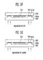
- FIGS. 4A to 4Eare sectional views illustrating a method of fabricating an organic light emitting display according to an embodiment of the present invention.
- first the transparent first frit layer 150ais formed on one region of the second substrate 200.
- the first frit layer 150ais made of at least one material selected from the group consisting of SiO 2 , B 2 O 3 , and P 2 O 5 .
- the first frit layer 150ais formed so as to increase the gap distance between the first substrate 100 and the second substrate 200 and to prevent Newton's rings from generating (FIG. 4A).
- the first frit layer 150ais sintered at a predetermined temperature.
- the temperature at which the frit layer 150a is sinteredis in the range of about 300°C to about 700°C.
- an opaque second frit layer 150bis formed on a region of the first frit layer 150a.
- the second frit layer 150bincludes an absorbent (not shown) for absorbing laser or infrared rays.
- the absorbentis one in which at least one material selected from a group consisting of SiO 2 , V 2 O 5 , and ZnO is added (FIG. 4C).
- the temperature at which the frit layer 150a is sinteredis in the range of about 300°C to about 550°C. In other words, the process of sintering the second frit layer 150b may be carried out at a temperature lower than that of sintering the first frit layer 150a. After this, the first substrate 100 is connected to the second substrate 200.
- an organic light emitting diodeincluding a first electrode (not shown), an organic material layer (not shown), and a second electrode (not shown) is formed, and after arranging the first substrate 100 and second substrate 200 such that the organic light emitting diodes (not shown) face the second substrate 200, the first substrate 100 is connected to the second substrate 200 (FIG. 4D).
- a laser or infrared beamis directed at the first frit layer 150a and the second frit layer 150b provided between the second substrate 200 and the first substrate 100 to bond the first frit layer 150a, the second frit layer 150b and the first substrate 100.
- a laser or infrared beamis directed at the first frit layer 150a and the second frit layer 150b provided between the second substrate 200 and the first substrate 100 to bond the first frit layer 150a, the second frit layer 150b and the first substrate 100.
- devices disposed between the first substrate 100 and the second substrate 200 including the organic light emitting diodeare sealed so that the devices can be protected from moisture or oxygen (FIG. 4E).
- the first sealing material 150may be formed on the first substrate 100 in certain embodiments.
- forming the second frit layer 150b on the first frit layer 150ahas been described such that a laser or infrared beam propagates via the transparent first frit layer 150a and is transmitted to the second frit layer 150b, the positions of the first frit layer 150a and the second frit layer 150b may be exchanged in certain embodiments.
- a sealing material 150 having the first frit layer 150a and the second frit layer 150bhas been described, the sealing material 150 may have more than two layers.
- FIGS. 5A to 5Gare sectional views illustrating a method of fabricating an organic light emitting display according to another embodiment of the present invention.
- first a transparent first frit layer 515ais formed on a region of a second substrate 520 so as to increase the gap distance between the first substrate 510 and the second substrate 520 and thus prevent the formation of Newton's rings.
- the first frit layer 515is made of at least one material selected from a group consisting of SiO 2 B 2 O 3 , and P 2 O 5 (FIG. 5A).
- the first frit layer 515ais sintered at a predetermined temperature in the range of about 300°C to about 700°C. Due to the sintering process of the first frit layer 515a, the interfaces of the second substrate 520 and the first frit layer 515a are bonded to each other (FIG. 5B).
- an opaque second frit layer 515bis formed on a region of the first frit layer 515a.
- the second frit layer 515bis one in which at least one material selected from a group consisting of SiO 2 PbO, V 2 O 5 , and ZnO is added.
- the second frit layer 151bis sintered to bond the interfaces of the first frit layer 515a and the second frit layer 515b to each other (FIG. 5C).
- a second sealing material 516comprising at least one resin selected from a group consisting of epoxy, acrylate, urethane acrylate, and cyanoacrylate is formed on the first frit layer 515a.
- the second sealing material 516may be formed on the first frit layer 515a to run parallel along both sides of the second frit layer 515b, may be formed to run parallel along the second frit layer 515b inside the second frit layer 515b on the first frit layer 515a, or may be formed to run parallel along the second frit layer 515b outside the second frit layer 515b on the first frit layer 515a.
- the second sealing material 515is provided at at least one of the inner and outer sides of the second frit layer 515b such that resistance against impact or shock is increased and adhesive force between the first substrate and the second substrate is increased.
- the first substrate 510is connected to the second substrate 520.
- an organic light emitting diodeincluding a first electrode (not shown), an organic material layer (not shown), and a second electrode (not shown) is formed, and after arranging the first substrate 510 and the second substrate 520 such that the organic light emitting diode (not sown) is disposed between the first substrate 510 and the second substrate 520, the first substrate 510 is connected to the second substrate 520 (FIG. 5E).
- ultraviolet raysare directed at the second sealing material 516 to cure the second sealing material 516 (FIG. 5F).
- a laser or infrared beamis directed at the first frit layer 515a and the second frit layer 515b provided between the second substrate 520 and the first substrate 510 to bond the first frit layer 515a, the second frit layer 515b and the first substrate 510.
- devices disposed between the first substrate 510 and the second substrate 520 including the organic light emitting diodeare sealed so that the devices can be protected from moisture or oxygen (FIG. 5G).
- Newton's ringscan be prevented by adjusting the distance between a first substrate and the second substrate.
- an epoxy-based second sealing materialis provided as an auxiliary sealing material to reinforce the device for shock-resistance and to effectively seal the organic light emitting diode.
Landscapes
- Chemical & Material Sciences (AREA)
- Engineering & Computer Science (AREA)
- Materials Engineering (AREA)
- Chemical Kinetics & Catalysis (AREA)
- General Chemical & Material Sciences (AREA)
- Geochemistry & Mineralogy (AREA)
- Life Sciences & Earth Sciences (AREA)
- Organic Chemistry (AREA)
- Physics & Mathematics (AREA)
- Optics & Photonics (AREA)
- Manufacturing & Machinery (AREA)
- Electroluminescent Light Sources (AREA)
- Devices For Indicating Variable Information By Combining Individual Elements (AREA)
Abstract
Description
- The present invention relates to organic light emitting display devices and, more particularly, to packaging such devices.
- Recently, organic light emitting displays that use organic light emitting diodes have been the subject of attention. Such organic light emitting displays are spontaneous emission displays that electrically excite phosphorous organic compounds to emit light and can be driven at a low voltage, can be easily made thin, and have a wide view angle and high response speed. The organic light emitting display includes a plurality of pixels that include organic light emitting diodes that are formed on a substrate and thin film transistors (TFT) for driving the organic light emitting diodes. Since the organic light emitting diodes are sensitive to moisture, a sealing structure in which moisture is prevented from contacting the organic materials by using a metal cap coated with an absorbent or a sealing glass substrate is provided.
U.S. Patent No. 6,998,776 B2 discloses that an organic light-emitting display includes a first substrate plate, a second substrate plate and a frit connecting the plates. - The invention sets out to solve the above problems and provides an organic light-emitting display device as set out in Claim 1. Preferred features of this invention are set out in Claims 2 to 23.
- Embodiments of the invention will now be described by way of example and with reference to the accompanying drawings in which:-
- FIG. 1 is a schematic plan view illustrating a second substrate employed in an organic light emitting display according to an embodiment of the present invention;
- FIG. 2 is a plan view illustrating an example of the second substrate employed in the organic light emitting display according to an embodiment of the present invention;
- FIG. 3 is a sectional view illustrating the organic light emitting display according to an embodiment of the present invention;
- FIGS. 4a to 4e are sectional views illustrating a method of fabricating an organic light emitting display according to an embodiment of the present invention;
- FIGS. 5 a to 5g are sectional views illustrating a method of fabricating an organic light emitting display according to an embodiment of the present invention;
- FIG. 6A is a schematic exploded view of a passive matrix type organic light emitting display device;
- FIG 6B is a schematic exploded view of an active matrix type organic light emitting display device;
- FIG. 6C is a schematic top plan view of an organic light emitting display device;
- FIG. 6D is a cross-sectional view of the organic light emitting display of FIG. 6C, taken along the line d-d; and
- FIG. 6E is a schematic perspective view illustrating mass production of organic light emitting devices;
- Hereinafter, embodiments of the present invention will be described in detail with reference to the accompanying drawings as follows.
- An organic light emitting display (OLED) is a display device comprising an array of organic light emitting diodes. Organic light emitting diodes are solid state devices which include an organic material and are adapted to generate and emit light when appropriate electrical potentials are applied.
- OLEDs can be generally grouped into two basic types dependent on the arrangement with which the stimulating electrical current is provided. Fig. 6A schematically illustrates an exploded view of a simplified structure of a passive
matrix type OLED 1000. Fig. 6B schematically illustrates a simplified structure of an activematrix type OLED 1001. In both configurations, the OLED 1000, 1001 includes OLED pixels built over asubstrate 1002, and the OLED pixels include ananode 1004, acathode 1006 and anorganic layer 1010. When an appropriate electrical current is applied to theanode 1004, electric current flows through the pixels and visible light is emitted from the organic layer. - Referring to Fig. 6A, the passive matrix OLED (PMOLED) design includes elongate strips of
anode 1004 arranged generally perpendicular to elongate strips ofcathode 1006 with organic layers interposed therebetween. The intersections of the strips ofcathode 1006 and anode 1004 define individual OLED pixels where light is generated and emitted upon appropriate excitation of the corresponding strips ofanode 1004 andcathode 1006. PMOLEDs provide the advantage of relatively simple fabrication. - Referring to Fig. 6B, the active matrix OLED (AMOLED) includes
local driving circuits 1012 arranged between thesubstrate 1002 and an array of OLED pixels. An individual pixel of AMOLEDs is defined between thecommon cathode 1006 and ananode 1004, which is electrically isolated from other anodes. Eachlocal driving circuit 1012 is coupled with ananode 1004 of the OLED pixels and further coupled with adata line 1016 and ascan line 1018. Thescan lines 1018 supply scan signals that select rows of the driving circuits, and thedata lines 1016 supply data signals for particular driving circuits. The data signals and scan signals stimulate thelocal driving circuits 1012, which excite theanodes 1004 so as to emit light from their corresponding pixels. - In the illustrated AMOLED, the
local driving circuits 1012, thedata lines 1016 andscan lines 1018 are buried in aplanarization layer 1014, which is interposed between the pixel array and thesubstrate 1002. Theplanarization layer 1014 provides a planar top surface on which the organic light emitting pixel array is formed. Theplanarization layer 1014 may be formed of organic or inorganic materials, and formed of two or more layers although shown as a single layer. Thelocal driving circuits 1012 are typically formed with thin film transistors (TFT) and arranged in a grid or array under the OLED pixel array. Thelocal driving circuits 1012 may be at least partly made of organic materials, including organic TFT. AMOLEDs have the advantage of fast response time improving their desirability for use in displaying data signals. Also, AMOLEDs have the advantages of consuming less power than passive matrix OLEDs. - Referring to common features of the PMOLED and AMOLED designs, the
substrate 1002 provides structural support for the OLED pixels and circuits. In various configurations, thesubstrate 1002 can comprise rigid or flexible materials as well as opaque or transparent materials, such as plastic, glass, and/or foil. As noted above, each OLED pixel or diode is formed with theanode 1004,cathode 1006 andorganic layer 1010 interposed therebetween. When an appropriate electrical current is applied to theanode 1004, thecathode 1006 injects electrons and theanode 1004 injects holes. In certain cases, theanode 1004 andcathode 1006 are inverted; i.e., the cathode is formed on thesubstrate 1002 and the anode is opposingly arranged. - Interposed between the
cathode 1006 andanode 1004 are one or more organic layers. More specifically, at least one emissive or light emitting layer is interposed between thecathode 1006 andanode 1004. The light emitting layer may comprise one or more light emitting organic compounds. Typically, the light emitting layer is configured to emit visible light in a single color such as blue, green, red or white. In the illustrated example, oneorganic layer 1010 is formed between thecathode 1006 andanode 1004 and acts as a light emitting layer. Additional layers, which can be formed between theanode 1004 andcathode 1006, can include a hole transporting layer, a hole injection layer, an electron transporting layer and an electron injection layer. - Hole transporting and/or injection layers can be interposed between the light emitting
layer 1010 and theanode 1004. Electron transporting and/or injecting layers can be interposed between thecathode 1006 and thelight emitting layer 1010. The electron injection layer facilitates injection of electrons from thecathode 1006 toward thelight emitting layer 1010 by reducing the work function for injecting electrons from thecathode 1006. Similarly, the hole injection layer facilitates injection of holes from theanode 1004 toward thelight emitting layer 1010. The hole and electron transporting layers facilitate movement of the carriers injected from the respective electrodes toward the light emitting layer. - In some cases, a single layer may serve both electron injection and transportation functions or both hole injection and transportation functions. In some structures, one or more of these layers are lacking. In some arrangements, one or more organic layers are doped with one or more materials that help injection and/or transportation of the carriers. In examples where only one organic layer is formed between the cathode and anode, the organic layer may include not only an organic light emitting compound but also certain functional materials that help injection or transportation of carriers within that layer.
- There are numerous organic materials that have been developed for use in these layers including the light emitting layer. Also, numerous other organic materials for use in these layers are being developed. In some cases, these organic materials may be macromolecules including oligomers and polymers. In some cases, the organic materials for these layers may be relatively small molecules. The skilled artisan will be able to select appropriate materials for each of these layers in view of the desired functions of the individual layers and the materials for the neighboring layers in particular designs.
- In operation, an electrical circuit provides appropriate potential between the
cathode 1006 andanode 1004. This results in an electrical current flowing from theanode 1004 to thecathode 1006 via the interposed organic layer(s). In one case, thecathode 1006 provides electrons to the adjacentorganic layer 1010. Theanode 1004 injects holes to theorganic layer 1010. The holes and electrons recombine in theorganic layer 1010 and generate energy particles called "excitons." The excitons transfer their energy to the organic light emitting material in theorganic layer 1010, and the energy is used to emit visible light from the organic light emitting material. The spectral characteristics of light generated and emitted by theOLED - OLED devices can also be categorized based on the direction of the light emission. In one type referred to as "top emission" type, OLED devices emit light and display images through the cathode or
top electrode 1006. In these structures, thecathode 1006 is made of a material transparent or at least partially transparent with respect to visible light. In certain cases, to avoid losing any light that can pass through the anode orbottom electrode 1004, the anode may be made of a material substantially reflective of the visible light. A second type of OLED devices emits light through the anode orbottom electrode 1004 and is called "bottom emission" type. In the bottom emission type OLED devices, theanode 1004 is made of a material which is at least partially transparent with respect to visible light. Often, in bottom emission type OLED devices, thecathode 1006 is made of a material substantially reflective of the visible light. A third type of OLED devices emits light in two directions, e.g. through bothanode 1004 andcathode 1006. Depending upon the direction(s) of the light emission, the substrate may be formed of a material which is transparent, opaque or reflective of visible light. - In many cases, an
OLED pixel array 1021 comprising a plurality of organic light emitting pixels is arranged over asubstrate 1002 as shown in Fig. 6C. The pixels in thearray 1021 are controlled to be turned on and off by a driving circuit (not shown), and the plurality of the pixels as a whole displays information or image on thearray 1021. In certain cases, theOLED pixel array 1021 is arranged with respect to other components, such as drive and control electronics to define a display region and a non-display region. In these structures, the display region refers to the area of thesubstrate 1002 whereOLED pixel array 1021 is formed. The non-display region refers to the remaining areas of thesubstrate 1002. The non-display region can contain logic and/or power supply circuitry. It will be understood that there will be at least portions of control/drive circuit elements arranged within the display region. For example, in PMOLEDs, conductive components will extend into the display region to provide appropriate potential to the anode and cathodes. In AMOLEDs, local driving circuits and data/scan lines coupled with the driving circuits will extend into the display region to drive and control the individual pixels of the AMOLEDs. - One design and fabrication consideration in OLED devices is that certain organic material layers of OLED devices can suffer damage or accelerated deterioration from exposure to water, oxygen or other harmful gases. Accordingly, it is generally understood that OLED devices be sealed or encapsulated to inhibit exposure to moisture and oxygen or other harmful gases found in a manufacturing or operational environment. Fig. 6D schematically illustrates a cross-section of an encapsulated
OLED device 1011 having a layout of Fig. 6C and taken along the line d-d of Fig. 6C. In this device, a generally planar top plate orsubstrate 1061 engages with aseal 1071 which further engages with a bottom plate orsubstrate 1002 to enclose or encapsulate theOLED pixel array 1021. In other structures, one or more layers are formed on thetop plate 1061 orbottom plate 1002, and theseal 1071 is coupled with the bottom ortop substrate seal 1071 extends along the periphery of theOLED pixel array 1021 or the bottom ortop plate - The
seal 1071 is made of a frit material as will be further discussed below. The top andbottom plates OLED pixel array 1021 from exposure to these substances. At least one of thetop plate 1061 and thebottom plate 1002 are formed of a substantially transparent material. - To lengthen the life time of
OLED devices 1011, it is generally desired thatseal 1071 and the top andbottom plates enclosed space 1081. In certain applications, it is indicated that theseal 1071 of a frit material in combination with the top andbottom plates enclosed space 1081, in some devices, a material that can take up oxygen and/or moisture is formed within the enclosedspace 1081. - The
seal 1071 has a width W, which is its thickness in a direction parallel to a surface of the top orbottom substrate seal 1071. In some cases, the width of theseal 1071 may be the largest where theseal 1071 contacts one of the bottom andtop substrate seal 1071 contacts the other. The width variation in a single cross-section of theseal 1071 relates to the cross-sectional shape of theseal 1071 and other design parameters. - The
seal 1071 has a height H, which is its thickness in a direction perpendicular to a surface of the top orbottom substrate seal 1071. However, in certain cases, the height of theseal 1071 may vary at different positions thereof. - In the illustrated device, the
seal 1071 has a generally rectangular cross-section. In other structures, however, theseal 1071 can have other various cross-sectional shapes such as a generally square cross-section, a generally trapezoidal cross-section, a cross-section with one or more rounded edges, or other configuration as indicated by the needs of a given application. To improve hermeticity, it is generally desired to increase the interfacial area where theseal 1071 directly contacts the bottom ortop substrate - The
seal 1071 can be arranged immediately adjacent theOLED array 1021, and in other cases, theseal 1071 is spaced some distance from theOLED array 1021. Theseal 1071 comprises generally linear segments that are connected together to surround theOLED array 1021. Such linear segments of theseal 1071 can extend, in certain cases, generally parallel to respective boundaries of theOLED array 1021. In other devices, one or more of the linear segments of theseal 1071 are arranged in a non-parallel relationship with respective boundaries of theOLED array 1021. In yet other devices, at least part of theseal 1071 extends between thetop plate 1061 andbottom plate 1002 in a curvilinear manner. - As noted above, in certain structures, the
seal 1071 is formed using a frit material or simply "frit" or glass frit," which includes fine glass particles. The frit particles includes one or more of magnesium oxide (MgO), calcium oxide (CaO), barium oxide (BaO), lithium oxide (Li2O), sodium oxide (Na2O), potassium oxide (K2O), boron oxide (B2O3), vanadium oxide (V2O5), zinc oxide (ZnO), tellurium oxide (TeO2), aluminum oxide (Al2O3), silicon dioxide (SiO2), lead oxide (PbO), tin oxide (SnO), phosphorous oxide (P2O5), ruthenium oxide (Ru2O), rubidium oxide (Rb2O), rhodium oxide (Rh2O), ferrite oxide (Fe2O3), copper oxide (CuO), titanium oxide (TiO2), tungsten oxide (WO3), bismuth oxide (Bi2O3), antimony oxide (Sb2O3), lead-borate glass, tin-phosphate glass, vanadate glass, and borosilicate, etc. Typically, these particles range in size from about 2 µm to about 30 µm, optionally about 5 µm to about 10 µm, although not limited only thereto. The particles can be as large as about the distance between the top andbottom substrates frit seal 1071 contacts. - The frit material used to form the
seal 1071 can also include one or more filler or additive materials. The filler or additive materials can be provided to adjust an overall thermal expansion characteristic of theseal 1071 and/or to adjust the absorption characteristics of theseal 1071 for selected frequencies of incident radiant energy. The filler or additive material(s) can also include inversion and/or additive fillers to adjust a coefficient of thermal expansion of the frit. For example, the filler or additive materials can include transition metals, such as chromium (Cr), iron (Fe), manganese (Mn), cobalt (Co), copper (Cu), and/or vanadium. Additional materials for the filler or additives include ZnSiO4, PbTiO3, ZrO2, eucryptite. - Typically, a frit material as a dry composition contains glass particles from about 20 to 90 about wt%, and the remainder includes fillers and/or additives. In some cases, the frit paste contains about 10-30 wt% organic materials and about 70-90% inorganic materials. In some cases, the frit paste contains about 20 wt% organic materials and about 80 wt% inorganic materials. In some cases, the organic materials may include about 0-30 wt% binder(s) and about 70-100 wt% solvent(s). In some cases, about 10 wt% is binder(s) and about 90 wt% is solvent(s) among the organic materials. In some cases, the inorganic materials may include about 0-10 wt% additives, about 20-40 wt% fillers and about 50-80 wt% glass powder. In some cases, about 0-5 wt% is additive(s), about 25-30 wt% is filler(s) and about 65-75 wt% is the glass powder among the inorganic materials.
- In forming a frit seal, a liquid material is added to the dry frit material to form a frit paste. Any organic or inorganic solvent with or without additives can be used as the liquid material. Typically, the solvent includes one or more organic compounds. For example, applicable organic compounds are ethyl cellulose, nitro cellulose, hydroxyl propyl cellulose, butyl carbitol acetate, terpineol, butyl cellusolve, acrylate compounds. Then, the thus formed frit paste can be applied to form a shape of the
seal 1071 on the top and/orbottom plate - In one case, a shape of the
seal 1071 is initially formed from the frit paste and interposed between thetop plate 1061 and thebottom plate 1002. Theseal 1071 can in certain cases be pre-cured or pre-sintered to one of the top plate andbottom plate top plate 1061 and thebottom plate 1002 with theseal 1071 interposed therebetween, portions of theseal 1071 are selectively heated such that the frit material forming theseal 1071 at least partially melts. Theseal 1071 is then allowed to resolidify to form a secure joint between thetop plate 1061 and thebottom plate 1002 to thereby inhibit exposure of the enclosedOLED pixel array 1021 to oxygen or water. - The selective heating of the frit seal is carried out by irradiation of light, such as a laser or directed infrared lamp. As previously noted, the frit material forming the
seal 1071 can be combined with one or more additives or filler such as species selected for improved absorption of the irradiated light to facilitate heating and melting of the frit material to form theseal 1071. - In some cases,
OLED devices 1011 are mass produced. In an embodiment illustrated in Fig. 6E, a plurality ofseparate OLED arrays 1021 is formed on a common bottom substrate 1101. In the illustrated example, eachOLED array 1021 is surrounded by a shaped frit to form theseal 1071. A common top substrate (not shown) is placed over the common bottom substrate 1101 and the structures formed thereon such that theOLED arrays 1021 and the shaped frit paste are interposed between the common bottom substrate 1101 and the common top substrate. TheOLED arrays 1021 are encapsulated and sealed, such as via the previously described enclosure process for a single OLED display device. The resulting product includes a plurality of OLED devices kept together by the common bottom and top substrates. Then, the resulting product is cut into a plurality of pieces, each of which constitutes anOLED device 1011 of Fig. 6D. In certain cases, theindividual OLED devices 1011 then further undergo additional packaging operations to further improve the sealing formed by thefrit seal 1071 and the top andbottom substrates - The organic light emitting display device has a gap between the top surface of the array and the inner surface of the top substrate. Generally, the size of the gap depends on the height of the seal interconnecting two substrates. The frit seal, among other forms of sealing, allows a gap size significantly smaller than others. For example, when using the frit seal, the gap size (the distance between the array and the second substrate) can be in the order of a few µm to several hundred µm. When the gap size is in this range, dark rings called Newton rings may be formed on the display surface due to optical interference created by light incident to the display surface. More specifically, when the gap size is about or less than 10 µm, the possibility of Newton rings may increase. Thus, in packaging an organic light emitting display device with the frit seal, the configuration for avoiding Newton rings can be a design factor.
- FIG. 1 is a schematic plan view illustrating a substrate employed in an organic light emitting display according to an embodiment of the present invention. As shown in FIG. 1, the organic light emitting display according to an embodiment of the present invention includes a first or
bottom substrate 100, a second ortop substrate 200, afirst sealing material 150, adata driver 300, ascan driver 400, and apad unit 500. Thefirst substrate 100 includes apixel region 100a in which a plurality of organic light emitting diodes or pixels (not shown) having a first electrode (not shown), an organic layer (not shown), and a second electrode (not shown) is formed, and anon-pixel region 100b formed in the outer circumference of thepixel region 100a. Thepixel region 100a includes a plurality of scan lines S1, S2, ..., and Sn arranged in the row direction and a plurality of data lines D1, D2, ..., and Dm arranged in the column direction, and a plurality ofpixels 50 is formed in the regions that are defined by the scan lines S1, S2, ..., and Sn and the data lines D1, D2, ..., and Dm. In other words, thepixel region 100a is a region where an image is displayed by a light emitted from an organic light emitting diode, and thenon-pixel region 100b represents all of the regions excluding thepixel region 100a on thefirst substrate 100. - The
second substrate 200 is attached to a region of thefirst substrate 100 that includes thepixel region 100a. In this case, thesecond substrate 200 is provided to prevent the organic light emitting diodes (not shown) formed on thepixel region 100a on thefirst substrate 100 from being affected by moisture and oxygen from the outside. Therefore, the organic light emitting diode formed on thefirst substrate 100 is sealed by thesecond substrate 200. In this case, although not limited thereto, thesecond substrate 200 may be formed of a material selected from the group consisting of SiO2, SiNx, and SiOxNy. - The sealing
material 150 is provided between thenon-pixel region 100b of thefirst substrate 100 and thesecond substrate 200. Consequently, since the gap between thefirst substrate 100 and thesecond substrate 200 is sealed up by thefirst sealing material 150, the organic light emitting diode provided between thefirst substrate 100 and thesecond substrate 200 can be protected from moisture and oxygen. At that time, thefirst sealing material 150 includes at least one a transparent first frit layer (not shown) and an opaque or non-transparent second frit layer (not shown). The first frit layer and the second frit layer will be described later in detail with reference to FIGS. 5a to 5e. - The
data driver 300 is made in the form of a chip, may be mounted on thefirst substrate 100, and is electrically connected to a second pad Pd of thepad unit 500. Thedata driver 300 supplies data signals to the plurality of data lines D1, D2, ..., and Dm. Thescan driver 400 is formed on one side of thepixel region 100a on thefirst substrate 100 and is electrically connected to at least one first pad Ps in thepad unit 500 by at least onescan supply line 410. Thescan driver 400 sequentially supplies scan signals to the plurality of scan lines S1, S2, ..., and Sn that extend in thepixel region 100a. Thepad unit 500 supplies driving power to thedata driver 300 through adata supply line 310 and to thescan driver 400 through ascan line 410. - In the illustrated embodiment, the sealing
material 150 is coated along the outer circumference of thepixel region 100a to seal only thepixel region 100a, although the invention is not limited to such an arrangement. Thefirst sealing material 150 may be applied to seal thepixel region 100a and thescan driver 400 when thescan driver 400 is built-in. In such an embodiment, the size of thesecond substrate 200 is sufficient to include thepixel region 100a and thescan driver 400. - FIG. 2 is a plan view illustrating the second substrate employed in this embodiment of the present invention. As shown in FIG. 2, the
second substrate 200 includes thefirst sealing material 150 provided along the edge thereof. Thefirst sealing material 150 includes at least one transparent first frit layer (not shown) and at least one opaque second frit layer (not shown). In this case, thefirst sealing material 150 is provided to protect the organic light emitting diodes formed on the first substrate (not shown) from moisture or oxygen and to seal up between thefirst substrate 100 and thesecond substrate 200. - FIG. 3 is a sectional view illustrating the organic light emitting display of this embodiment of the present invention. As shown in FIG. 3, the organic light emitting display includes the
first substrate 100, thefirst sealing material 150, and thesecond substrate 200. Thefirst substrate 100 includes adeposition substrate 101 and at least one organiclight emitting diode 110 formed on thedeposition substrate 101. First, abuffer layer 111 is formed on thedeposition substrate 101. Thedeposition substrate 101 is formed of glass and thebuffer layer 111 is formed of an insulating material such as SiO2 and SiNx. On the other hand, thebuffer layer 111 is formed to prevent thedeposition substrate 101 from being damaged by factors such as heat from the outside. - A
semiconductor layer 112 that includes anactive layer 112a and source/drain regions 112b is formed on at least one region of thebuffer layer 111. Agate insulation layer 113 is formed on thebuffer layer 111 to include thesemiconductor layer 112. Agate electrode 114 of the size corresponding to the width of anactive layer 112a is formed on one region of thegate insulation layer 113. Aninterlayer insulation layer 115 is formed on thegate insulation layer 113 to include thegate electrode 114. Source anddrain electrodes interlayer insulation layer 115. Each of the source anddrain electrodes drain regions 112b. A planarization layer 117 is formed on theinterlayer insulation layer 115 to include the source anddrain electrodes first electrode 119 is formed on one region of the planarization layer 117. In this case, thefirst electrode 119 is connected to an exposed region of one of thedrain electrode 116b by a viahole 118. In alternative embodiments a connection may be made to thesource electrode 116a. A pixel definition layer 120 including an aperture (not shown) that exposes at least one region of thefirst electrode 119 is formed on the planarization layer 117 to include thefirst electrode 119. Anorganic layer 121 is formed on the aperture of the pixel definition layer 120 and asecond electrode layer 122 is formed on the pixel definition layer 120 to include theorganic layer 121. - The
second substrate 200 is attached to thefirst substrate 100 by thefirst sealing material 150 with predetermined structures interposed in order to protect the predetermined structures formed on thefirst substrate 100 against the oxygen and moisture from the outside. Thesecond substrate 200 is made of SiO2. - The
first sealing material 150 includes afirst frit layer 150a and asecond frit layer 150b. Thesecond frit layer 150b melts substantially easier than thefirst frit layer 150a upon application of a laser or infrared beam thereto. In one embodiment, when all other conditions are the same, the composition of materials forming thesecond frit layer 150b melts more quickly than the composition of materials forming thefirst frit layer 150a. For example, the time required to start the melting of thesecond frit layer 150b is about 10, 20, 30, 40, 50, 55, 60, 65, 70, 75, 80 or 90 % of the time required to start the melting of thefirst frit layer 150a. In another embodiment, when all other conditions are the same, the composition of materials forming thesecond frit layer 150b melts when subjected to a less powerful beam than the composition of materials forming thefirst frit layer 150a. For example, the energy of the laser or infrared beam required to start the melting of thesecond frit layer 150b is about 10, 20, 30, 40, 50, 55, 60, 65, 70, 75, 80 or 90 % of the energy of the beam required to start the melting of thefirst frit layer 150a when applied for the same period of time. Thefirst frit layer 150a may be transparent and thesecond frit layer 150b may be opaque. - The
first sealing material 150 is provided between thenon-pixel region 100b of thefirst substrate 100 and thesecond substrate 200 to attach thefirst substrate 100 and thesecond substrate 200 to each other. That is, since the gap between thefirst substrate 100 and thesecond substrate 200 is sealed up by thefirst sealing material 150, the organic light emitting diodes that are interposed between the first substrate and thesecond substrate 200 are protected from moisture and oxygen. Also, thefrit 150 is hardened by irradiating the laser or infrared rays onto thefrit 150. At this time, the intensity of the laser radiated onto thefrit 150 is in the range of about 25 W to about 60 W. - When the temperature of heated glass is rapidly reduced, a frit in the form of glass powders is generated. In general, oxide powders are added to the glass powders to be used. When an organic material is added to the frit, a gel-type paste is obtained. At this time, when the gel-type paste is sintered at a predetermined temperature, the organic material is extinguished in the air and the gel-type paste is hardened so that a glass frit is obtained.
- Newton's rings may appear as concentric circles in display surfaces. The Newton's rings may be generated when the distance between the
first substrate 100 and thesecond substrate 200 is small. Therefore, in order to prevent the Newton's ring, there is a need to increase the gap distance between thefirst substrate 100 and thesecond substrate 200 by a predetermined height. Thefirst frit layer 150a is consequently formed to prevent Newton's rings by way of increasing a gap between thefirst substrate 100 and thesecond substrate 200. The width W1 of thefirst frit layer 150a is from about 0.5 mm to about 1.5 mm. (See Fig. 3.) - The
second frit layer 150b includes a filler (not shown) for adjusting a thermal expansion coefficient and an absorbent (not shown) for absorbing laser and infrared rays. Thesecond frit layer 150b consequently serves as an absorbing layer of laser or infrared rays. The laser or the infrared rays are irradiated to bond the first sealing material for sealing the gap between thefirst substrate 100 and thesecond substrate 200, and the laser or infrared beam is substantially absorbed by thesecond frit layer 150b. - In certain embodiments, the
first frit layer 150a is a component for increasing the gap distance between thefirst substrate 100 and thesecond substrate 200, and the laser or the infrared rays are transmitted via thefirst frit layer 150a and are projected to thesecond frit layer 150b. Thefirst frit layer 150a for increasing the gap distance is provided to have a height H1 greater than a height H2 of thesecond frit layer 150b. (See Fig. 3.). In this particular case, thefirst frit layer 150a has a height H1 of 5 µm to 500 µm, and thesecond frit layer 150b has a height H2 of 3 µm to 100 µm, although the invention is not limited to these dimensions. - FIGS. 4A to 4E are sectional views illustrating a method of fabricating an organic light emitting display according to an embodiment of the present invention. Referring to FIGS. 4A to 4E, in the method of fabricating an organic light emitting display, first the transparent
first frit layer 150a is formed on one region of thesecond substrate 200. Thefirst frit layer 150a is made of at least one material selected from the group consisting of SiO2, B2O3, and P2O5. Thefirst frit layer 150a is formed so as to increase the gap distance between thefirst substrate 100 and thesecond substrate 200 and to prevent Newton's rings from generating (FIG. 4A). - After this, the
first frit layer 150a is sintered at a predetermined temperature. The temperature at which thefrit layer 150a is sintered is in the range of about 300°C to about 700°C. After the sintering of thefirst frit layer 150a, the interfaces of thesecond substrate 200 and thefirst frit layer 150a are adhered to each other (FIG. 4B). - As a following process, an opaque
second frit layer 150b is formed on a region of thefirst frit layer 150a. At this time, thesecond frit layer 150b includes an absorbent (not shown) for absorbing laser or infrared rays. The absorbent is one in which at least one material selected from a group consisting of SiO2, V2O5, and ZnO is added (FIG. 4C). The temperature at which thefrit layer 150a is sintered is in the range of about 300°C to about 550°C. In other words, the process of sintering thesecond frit layer 150b may be carried out at a temperature lower than that of sintering thefirst frit layer 150a. After this, thefirst substrate 100 is connected to thesecond substrate 200. At this time, on thefirst substrate 100, at least an organic light emitting diode (not shown) including a first electrode (not shown), an organic material layer (not shown), and a second electrode (not shown) is formed, and after arranging thefirst substrate 100 andsecond substrate 200 such that the organic light emitting diodes (not shown) face thesecond substrate 200, thefirst substrate 100 is connected to the second substrate 200 (FIG. 4D). - After that, a laser or infrared beam is directed at the
first frit layer 150a and thesecond frit layer 150b provided between thesecond substrate 200 and thefirst substrate 100 to bond thefirst frit layer 150a, thesecond frit layer 150b and thefirst substrate 100. By doing so, devices disposed between thefirst substrate 100 and thesecond substrate 200 including the organic light emitting diode are sealed so that the devices can be protected from moisture or oxygen (FIG. 4E). - Although the
first sealing material 150 being formed on thesecond substrate 200 has been described, thefirst sealing material 150 may be formed on thefirst substrate 100 in certain embodiments. Although, forming thesecond frit layer 150b on thefirst frit layer 150a has been described such that a laser or infrared beam propagates via the transparentfirst frit layer 150a and is transmitted to thesecond frit layer 150b, the positions of thefirst frit layer 150a and thesecond frit layer 150b may be exchanged in certain embodiments. Further, although a sealingmaterial 150 having thefirst frit layer 150a and thesecond frit layer 150b has been described, the sealingmaterial 150 may have more than two layers. - FIGS. 5A to 5G are sectional views illustrating a method of fabricating an organic light emitting display according to another embodiment of the present invention. Referring to FIGS. 5A to 5G, in the method of fabricating an organic light emitting, first a transparent
first frit layer 515a is formed on a region of asecond substrate 520 so as to increase the gap distance between thefirst substrate 510 and thesecond substrate 520 and thus prevent the formation of Newton's rings. In this case, the first frit layer 515 is made of at least one material selected from a group consisting of SiO2 B2O3, and P2O5 (FIG. 5A). After this, thefirst frit layer 515a is sintered at a predetermined temperature in the range of about 300°C to about 700°C. Due to the sintering process of thefirst frit layer 515a, the interfaces of thesecond substrate 520 and thefirst frit layer 515a are bonded to each other (FIG. 5B). - As a following process, an opaque
second frit layer 515b is formed on a region of thefirst frit layer 515a. Thesecond frit layer 515b is one in which at least one material selected from a group consisting of SiO2 PbO, V2O5, and ZnO is added. After this, the second frit layer 151b is sintered to bond the interfaces of thefirst frit layer 515a and thesecond frit layer 515b to each other (FIG. 5C). - After this, a
second sealing material 516 comprising at least one resin selected from a group consisting of epoxy, acrylate, urethane acrylate, and cyanoacrylate is formed on thefirst frit layer 515a. Thesecond sealing material 516, as illustrated in the drawings, may be formed on thefirst frit layer 515a to run parallel along both sides of thesecond frit layer 515b, may be formed to run parallel along thesecond frit layer 515b inside thesecond frit layer 515b on thefirst frit layer 515a, or may be formed to run parallel along thesecond frit layer 515b outside thesecond frit layer 515b on thefirst frit layer 515a. As such, the second sealing material 515 is provided at at least one of the inner and outer sides of thesecond frit layer 515b such that resistance against impact or shock is increased and adhesive force between the first substrate and the second substrate is increased. - After this, the
first substrate 510 is connected to thesecond substrate 520. At this time, on thefirst substrate 510, at least an organic light emitting diode (not shown) including a first electrode (not shown), an organic material layer (not shown), and a second electrode (not shown) is formed, and after arranging thefirst substrate 510 and thesecond substrate 520 such that the organic light emitting diode (not sown) is disposed between thefirst substrate 510 and thesecond substrate 520, thefirst substrate 510 is connected to the second substrate 520 (FIG. 5E). - As a following process, ultraviolet rays are directed at the
second sealing material 516 to cure the second sealing material 516 (FIG. 5F). After this, a laser or infrared beam is directed at thefirst frit layer 515a and thesecond frit layer 515b provided between thesecond substrate 520 and thefirst substrate 510 to bond thefirst frit layer 515a, thesecond frit layer 515b and thefirst substrate 510. By doing so, devices disposed between thefirst substrate 510 and thesecond substrate 520 including the organic light emitting diode are sealed so that the devices can be protected from moisture or oxygen (FIG. 5G). - In an organic light emitting display device and the method of fabricating the same according to the present invention, Newton's rings can be prevented by adjusting the distance between a first substrate and the second substrate. Moreover, an epoxy-based second sealing material is provided as an auxiliary sealing material to reinforce the device for shock-resistance and to effectively seal the organic light emitting diode.
- Although certain embodiments of the present invention have been shown and described, it would be appreciated by those skilled in the art that changes might be made in this embodiment without departing from the principles of the invention, the scope of which is defined in the claims and their equivalents.
Claims (23)
- An organic light emitting display device, comprising:a first substrate made of a single layer or multiple layers;a second substrate made of a single layer or multiple layers and opposing the first substrate;an array of organic light emitting pixels interposed between the first and second substrates; anda frit seal comprising a plurality of elongated segments, which forms a closed loop surrounding the array and interposed between the first and second substrates, wherein the frit seal, the first substrate and the second substrate together define an enclosed space in which the array is located, wherein the frit seal comprises a first frit portion contacting the first substrate and a second frit portion contacting the second substrate, wherein a first one of the plurality of segments comprises the first and second frit portions, wherein the second frit portion is configured to melt substantially more easily than the first frit portion upon the application of a laser or infrared beam thereto.
- A device according to Claim 1, wherein the first and second frit portions contact each other.
- A device according to Claim 1 or 2, wherein each of the first and second frit portions comprises a light-to-heat conversion material configured to generate heat upon receiving the laser or infrared beam, and wherein the second frit portion comprises a substantially greater amount of the light-to-heat conversion material than the first frit portion.
- A device according to Claim 1 or 2, wherein the second frit portion comprises a light-to-heat conversion material configured to generate heat upon receiving the laser or infrared beam, and wherein the first frit portion is substantially free of the light-to-heat conversion material.
- A device according to any preceding claim, wherein the first frit portion is substantially transparent.
- A device according to any preceding claim, wherein the second frit portion is substantially non-transparent.
- A device according to any preceding claim, wherein one of the first and second frit portions comprises at least one material selected from the group consisting of SiO2, PbO, V2O5, ZnO, B2O3, and P2O5.
- A device according to any preceding claim, wherein the first frit portion comprises a first end facing the second substrate, the second frit portion comprises a second end facing the first substrate, wherein the first end has a first width perpendicular to the shortest imaginary line interconnecting the first and second substrates in a plane perpendicular to a major axis of the first segment, and wherein the second end has a second width in the same direction, wherein the first width is greater than the second width.
- A device according to Claim 8, wherein the second end contacts a peripheral portion of the first end along the direction.
- A device according to Claim 8, wherein the second end contacts a central portion of the first end along the direction.
- A device according to any preceding claim, wherein the first frit portion comprises a first end facing the second substrate, the second frit portion comprises a second end facing the first substrate, wherein the first portion has a first height from the first substrate to the first end in a direction parallel to the shortest imaginary line interconnecting the first and second substrates in a plane perpendicular to a major axis of the first segment, wherein the second portion has a second height from the second substrate to the second end in the same direction, wherein the first height is greater than the second height.
- A device according to any preceding claim, wherein the array is formed on the second substrate, and wherein the array and the first substrate form a gap therebetween.
- A device according to any preceding claim, wherein the device is configured to display image through the first substrate.
- A device according to any preceding claim, wherein the first frit portion has a volume substantially greater than that of the second frit portion.
- A device according to any preceding claim wherein the first frit portion is bonded to the first substrate by baking the first substrate and the first frit portion in contact with the first substrate.
- A device according to any preceding claim, wherein the second frit portion is bonded to the second substrate and the first frit portion by applying a laser or infrared light thereto.
- A device according to any preceding claim, further comprising at least one supplementary structure extending along the first segment, wherein the at least one supplementary structure is interposed between and interconnects the first and second substrates, wherein the supplementary structure is located inside or outside the enclosed space.
- A device according to Claim 17, wherein the supplementary structure is configured to improve sealing of the enclosed space.
- A device according to one of Claims 1 to 16 comprising a first supplementary structure and a second supplementary structure, each of which is interposed between and interconnects the first and second substrates, wherein the first supplementary structure extends along the first segment inside the enclosed space, and wherein the second supplementary structure extends along the first segment outside the enclosed space.
- A device according to any preceding claim, further comprising a supplementary structure extending along the first segment and located inside or outside the enclosed space, wherein the supplementary structure comprises a portion interposed between and interconnecting the first frit portion and the second substrate.
- A device according to Claim 20, wherein the supplementary structure comprises another portion that is not interposed between the first frit portion of the frit seal and the first substrates.
- A device according to any preceding claim, further comprising a first supplementary structure and a second supplementary structure, each of which extends along the first segment inside or outside the enclosed space, wherein the first supplementary structure is interposed between and interconnects the first and second substrates, wherein the second supplementary structure is interposed between and interconnects the first frit portion and the second substrate.
- A device according to any preceding claim, wherein the frit seal comprises one or more materials selected from the group consisting of magnesium oxide (MgO), calcium oxide (CaO), barium oxide (BaO), lithium oxide (Li2O), sodium oxide (Na2O), potassium oxide (K2O), boron oxide (B2O3), vanadium oxide (V2O5), zinc oxide (ZnO), tellurium oxide (TeO2), aluminum oxide (Al2O3), silicon dioxide (SiO2), lead oxide (PbO), tin oxide (SnO), phosphorous oxide (P2O5), ruthenium oxide (Ru2O), rubidium oxide (Rb2O), rhodium oxide (Rh2O), ferrite oxide (Fe2O3), copper oxide (CuO), titanium oxide (TiO2), tungsten oxide (WO3), bismuth oxide (Bi2O3), antimony oxide (Sb2O3), lead-borate glass, tin-phosphate glass, vanadate glass, and borosilicate.
Applications Claiming Priority (1)
| Application Number | Priority Date | Filing Date | Title |
|---|---|---|---|
| KR1020060008761AKR100688790B1 (en) | 2006-01-27 | 2006-01-27 | Organic electroluminescent display and manufacturing method thereof |
Publications (2)
| Publication Number | Publication Date |
|---|---|
| EP1814186A2true EP1814186A2 (en) | 2007-08-01 |
| EP1814186A3 EP1814186A3 (en) | 2011-08-31 |
Family
ID=38007082
Family Applications (1)
| Application Number | Title | Priority Date | Filing Date |
|---|---|---|---|
| EP07250355AWithdrawnEP1814186A3 (en) | 2006-01-27 | 2007-01-29 | Organic light emitting display and method of fabricating the same |
Country Status (6)
| Country | Link |
|---|---|
| US (1) | US8125146B2 (en) |
| EP (1) | EP1814186A3 (en) |
| JP (1) | JP4554554B2 (en) |
| KR (1) | KR100688790B1 (en) |
| CN (1) | CN100524806C (en) |
| TW (1) | TWI359624B (en) |
Cited By (5)
| Publication number | Priority date | Publication date | Assignee | Title |
|---|---|---|---|---|
| EP2197240A1 (en)* | 2008-10-29 | 2010-06-16 | Samsung Mobile Display Co., Ltd. | Light emitting display and method of manufacturing the same |
| US7992411B2 (en) | 2008-05-30 | 2011-08-09 | Corning Incorporated | Method for sintering a frit to a glass plate |
| US8147632B2 (en) | 2008-05-30 | 2012-04-03 | Corning Incorporated | Controlled atmosphere when sintering a frit to a glass plate |
| EP2157832A4 (en)* | 2007-03-29 | 2012-08-01 | Fujifilm Corp | ELECTRONIC DEVICE AND METHOD FOR MANUFACTURING THE SAME |
| EP3648191A1 (en)* | 2018-11-05 | 2020-05-06 | Samsung Display Co., Ltd. | Display device and method of fabricating the same |
Families Citing this family (73)
| Publication number | Priority date | Publication date | Assignee | Title |
|---|---|---|---|---|
| US8038495B2 (en) | 2006-01-20 | 2011-10-18 | Samsung Mobile Display Co., Ltd. | Organic light-emitting display device and manufacturing method of the same |
| KR100673765B1 (en) | 2006-01-20 | 2007-01-24 | 삼성에스디아이 주식회사 | Organic light emitting display device and manufacturing method |
| KR100635514B1 (en) | 2006-01-23 | 2006-10-18 | 삼성에스디아이 주식회사 | Organic light emitting display device and manufacturing method |
| JP4624309B2 (en)* | 2006-01-24 | 2011-02-02 | 三星モバイルディスプレイ株式會社 | Organic electroluminescent display device and manufacturing method thereof |
| JP4456092B2 (en)* | 2006-01-24 | 2010-04-28 | 三星モバイルディスプレイ株式會社 | Organic electroluminescent display device and manufacturing method thereof |
| KR100688795B1 (en)* | 2006-01-25 | 2007-03-02 | 삼성에스디아이 주식회사 | Organic light emitting display device and manufacturing method |
| KR100685853B1 (en)* | 2006-01-25 | 2007-02-22 | 삼성에스디아이 주식회사 | Organic light emitting display device and manufacturing method |
| KR100688796B1 (en)* | 2006-01-25 | 2007-03-02 | 삼성에스디아이 주식회사 | Organic light emitting display device and manufacturing method thereof |
| KR100671641B1 (en) | 2006-01-25 | 2007-01-19 | 삼성에스디아이 주식회사 | Organic electroluminescent display and manufacturing method thereof |
| US8164257B2 (en)* | 2006-01-25 | 2012-04-24 | Samsung Mobile Display Co., Ltd. | Organic light emitting display and method of fabricating the same |
| JP4633674B2 (en) | 2006-01-26 | 2011-02-16 | 三星モバイルディスプレイ株式會社 | Organic electroluminescent display device and manufacturing method thereof |
| KR100732808B1 (en)* | 2006-01-26 | 2007-06-27 | 삼성에스디아이 주식회사 | Manufacturing method of organic light emitting display device |
| KR100671647B1 (en)* | 2006-01-26 | 2007-01-19 | 삼성에스디아이 주식회사 | Organic light emitting display device |
| KR100671639B1 (en)* | 2006-01-27 | 2007-01-19 | 삼성에스디아이 주식회사 | Organic electroluminescent display and manufacturing method thereof |
| KR100732817B1 (en) | 2006-03-29 | 2007-06-27 | 삼성에스디아이 주식회사 | Organic light emitting display device and manufacturing method |
| US20090044496A1 (en)* | 2007-08-16 | 2009-02-19 | Botelho John W | Method and apparatus for sealing a glass package |
| KR100840117B1 (en) | 2007-09-05 | 2008-06-19 | 삼성에스디아이 주식회사 | Light emitting display device and manufacturing method thereof |
| WO2010055888A1 (en) | 2008-11-14 | 2010-05-20 | 旭硝子株式会社 | Method for producing glass member provided with sealing material layer, and method for manufacturing electronic device |
| SG171754A1 (en)* | 2008-12-12 | 2011-07-28 | Asahi Glass Co Ltd | Sealing glass, glass member provided with sealing material layer, electronic device and process for producing it |
| DE102008063636A1 (en)* | 2008-12-18 | 2010-06-24 | Osram Opto Semiconductors Gmbh | Method for producing an organic optoelectronic component and organic optoelectronic component |
| KR20120104922A (en) | 2009-06-30 | 2012-09-24 | 아사히 가라스 가부시키가이샤 | Glass member with sealing material layer, electronic device using same, and method for manufacturing the electronic device |
| KR101155896B1 (en)* | 2009-11-20 | 2012-06-20 | 삼성모바일디스플레이주식회사 | Organic light emitting diode display and method for manufacturing the same |
| JP5407819B2 (en)* | 2009-12-07 | 2014-02-05 | 凸版印刷株式会社 | Organic electroluminescence display and manufacturing method thereof |
| JP2011222448A (en)* | 2010-04-14 | 2011-11-04 | Panasonic Electric Works Co Ltd | Method for manufacturing light-emitting device |
| EP2564471B1 (en)* | 2010-04-27 | 2021-01-20 | Ferro Corporation | Hermetic sealing of glass plates |
| US9171721B2 (en) | 2010-10-26 | 2015-10-27 | Medtronic, Inc. | Laser assisted direct bonding |
| US8666505B2 (en) | 2010-10-26 | 2014-03-04 | Medtronic, Inc. | Wafer-scale package including power source |
| US8796109B2 (en) | 2010-12-23 | 2014-08-05 | Medtronic, Inc. | Techniques for bonding substrates using an intermediate layer |
| US8545281B2 (en)* | 2011-04-13 | 2013-10-01 | Semiconductor Energy Laboratory Co., Ltd. | Method for manufacturing electroluminesccent device |
| TWI743509B (en) | 2011-05-05 | 2021-10-21 | 日商半導體能源研究所股份有限公司 | Semiconductor device and method for manufacturing the same |
| JP5947098B2 (en) | 2011-05-13 | 2016-07-06 | 株式会社半導体エネルギー研究所 | Method for manufacturing glass sealed body and method for manufacturing light-emitting device |
| KR102038844B1 (en) | 2011-06-16 | 2019-10-31 | 가부시키가이샤 한도오따이 에네루기 켄큐쇼 | Sealed body, method for manufacturing sealed body, light-emitting device, and method for manufacturing light-emitting device |
| JP6111022B2 (en)* | 2011-06-17 | 2017-04-05 | 株式会社半導体エネルギー研究所 | Method for manufacturing sealing body and method for manufacturing light-emitting device |
| JP5816029B2 (en) | 2011-08-24 | 2015-11-17 | 株式会社半導体エネルギー研究所 | Light emitting device |
| WO2013031509A1 (en) | 2011-08-26 | 2013-03-07 | Semiconductor Energy Laboratory Co., Ltd. | Light-emitting device, electronic device, lighting device, and method for manufacturing the light-emitting device |
| US9472776B2 (en) | 2011-10-14 | 2016-10-18 | Semiconductor Energy Laboratory Co., Ltd. | Method for manufacturing sealed structure including welded glass frits |
| JP2013101923A (en) | 2011-10-21 | 2013-05-23 | Semiconductor Energy Lab Co Ltd | Method of heating dispersion composition and method of forming glass pattern |
| KR102058387B1 (en) | 2011-11-28 | 2019-12-24 | 가부시키가이샤 한도오따이 에네루기 켄큐쇼 | Glass pattern and method for forming the same, sealed body and method for manufacturing the same, and light-emitting device |
| TWI569490B (en) | 2011-11-28 | 2017-02-01 | 半導體能源研究所股份有限公司 | Sealing body, light emitting module, and method of manufacturing the same |
| KR20130060131A (en) | 2011-11-29 | 2013-06-07 | 가부시키가이샤 한도오따이 에네루기 켄큐쇼 | Sealed structure, light-emitting device, electronic device, and lighting device |
| KR102001815B1 (en) | 2011-11-29 | 2019-07-19 | 가부시키가이샤 한도오따이 에네루기 켄큐쇼 | Method of manufacturing sealed body and method of manufacturing light-emitting device |
| TWI570906B (en) | 2011-11-29 | 2017-02-11 | 半導體能源研究所股份有限公司 | Sealing structure, illuminating device, electronic device, and lighting device |
| KR20140016170A (en) | 2012-07-30 | 2014-02-07 | 가부시키가이샤 한도오따이 에네루기 켄큐쇼 | Sealing structure and organic electroluminescence device |
| CN103681482A (en)* | 2012-09-21 | 2014-03-26 | 上海天马微电子有限公司 | OLED display device and packaging method thereof |
| US9362522B2 (en) | 2012-10-26 | 2016-06-07 | Semiconductor Energy Laboratory Co., Ltd. | Method for bonding substrates, method for manufacturing sealing structure, and method for manufacturing light-emitting device |
| KR20140061095A (en)* | 2012-11-13 | 2014-05-21 | 삼성디스플레이 주식회사 | Organic light emitting display apparatus and method of manufacturing the same |
| TWI479464B (en) | 2013-05-09 | 2015-04-01 | Au Optronics Corp | Display panel and packaging method thereof |
| KR102114154B1 (en)* | 2013-07-02 | 2020-05-25 | 삼성디스플레이 주식회사 | Display apparatus |
| KR102035252B1 (en) | 2013-09-03 | 2019-11-11 | 삼성디스플레이 주식회사 | Display device including sealant and manufacturing method thereof |
| CN103794637B (en)* | 2014-02-24 | 2016-08-24 | 上海和辉光电有限公司 | Active matrix organic light emitting diode panel and packaging method thereof |
| US9660004B2 (en)* | 2014-03-21 | 2017-05-23 | Apple Inc. | Flexible displays with strengthened pad area |
| KR101549406B1 (en)* | 2014-04-04 | 2015-09-03 | 코닝정밀소재 주식회사 | Substrate for color conversion of led and method of fabricating threof |
| US9073488B1 (en)* | 2014-05-30 | 2015-07-07 | Nissan North America, Inc. | Vehicle body structure |
| CN104269497B (en)* | 2014-09-03 | 2017-01-18 | 深圳市华星光电技术有限公司 | Organic light-emitting diode packaging structure and display device |
| US10457595B2 (en) | 2014-10-31 | 2019-10-29 | Corning Incorporated | Laser welded glass packages |
| KR20160076002A (en)* | 2014-12-19 | 2016-06-30 | 삼성디스플레이 주식회사 | Display device and manufacturing method thereof |
| US9968794B2 (en) | 2014-12-24 | 2018-05-15 | Medtronic, Inc. | Implantable medical device system including feedthrough assembly and method of forming same |
| US10136535B2 (en) | 2014-12-24 | 2018-11-20 | Medtronic, Inc. | Hermetically-sealed packages including feedthrough assemblies |
| US9865533B2 (en) | 2014-12-24 | 2018-01-09 | Medtronic, Inc. | Feedthrough assemblies |
| US10124559B2 (en) | 2014-12-24 | 2018-11-13 | Medtronic, Inc. | Kinetically limited nano-scale diffusion bond structures and methods |
| CN104538561B (en) | 2015-01-13 | 2016-08-31 | 京东方科技集团股份有限公司 | Method for packing, display floater and display device |
| CN106206960A (en)* | 2015-04-29 | 2016-12-07 | 上海和辉光电有限公司 | A kind of encapsulating structure and preparation method thereof |
| CN104810484B (en)* | 2015-05-07 | 2017-01-04 | 合肥鑫晟光电科技有限公司 | Packaging plastic, method for packing, display floater and display device |
| US10098589B2 (en) | 2015-12-21 | 2018-10-16 | Medtronic, Inc. | Sealed package and method of forming same |
| CN107275515B (en)* | 2017-06-20 | 2019-12-03 | 深圳市华星光电技术有限公司 | OLED device packaging method, structure, OLED device and display screen |
| KR102391994B1 (en)* | 2017-08-14 | 2022-04-28 | 삼성디스플레이 주식회사 | Multi stack joined body, method of manufacturing the multi stack joined body, and display device comprising multi stack joined body |
| KR102566338B1 (en)* | 2018-04-13 | 2023-08-11 | 삼성디스플레이 주식회사 | Display device and method for manufacturing display device |
| KR102566157B1 (en)* | 2018-06-28 | 2023-08-11 | 삼성디스플레이 주식회사 | Display device |
| WO2020071026A1 (en)* | 2018-10-02 | 2020-04-09 | ソニーセミコンダクタソリューションズ株式会社 | Display device and electronic device |
| KR102624165B1 (en) | 2018-10-12 | 2024-01-12 | 삼성디스플레이 주식회사 | Display device and manufacturing method for the display device |
| CN110649180B (en)* | 2019-09-30 | 2021-10-26 | 武汉天马微电子有限公司 | Display panel manufacturing method, display panel and display device |
| KR20210121357A (en)* | 2020-03-27 | 2021-10-08 | 삼성디스플레이 주식회사 | Display device and method for manufacturing the same |
| CN118412412A (en)* | 2024-06-27 | 2024-07-30 | 惠科股份有限公司 | Method for manufacturing light-emitting element and display device |
Citations (4)
| Publication number | Priority date | Publication date | Assignee | Title |
|---|---|---|---|---|
| JPH1074583A (en)* | 1996-08-30 | 1998-03-17 | Sanyo Electric Co Ltd | Organic EL display and method of manufacturing organic EL display |
| US20030066311A1 (en)* | 2001-10-09 | 2003-04-10 | Chien-Hsing Li | Encapsulation of a display element and method of forming the same |
| US20040207314A1 (en)* | 2003-04-16 | 2004-10-21 | Aitken Bruce G. | Glass package that is hermetically sealed with a frit and method of fabrication |
| US20050269926A1 (en)* | 2004-05-27 | 2005-12-08 | Nobuhiko Fukuoka | Organic electroluminescence display apparatus and method for manufacturing the same |
Family Cites Families (141)
| Publication number | Priority date | Publication date | Assignee | Title |
|---|---|---|---|---|
| US3966449A (en)* | 1975-02-10 | 1976-06-29 | International Business Machines Corporation | Sealing glass composition and process |
| US4105292A (en)* | 1975-09-02 | 1978-08-08 | Minnesota Mining And Manufacturing Company | Optical element to assure a minimum spacing |
| US4238704A (en) | 1979-02-12 | 1980-12-09 | Corning Glass Works | Sealed beam lamp of borosilicate glass with a sealing glass of zinc silicoborate and a mill addition of cordierite |
| JPS5966157A (en)* | 1982-10-08 | 1984-04-14 | Fujitsu Ltd | Semiconductor device and its manufacturing method |
| JPH0682765B2 (en)* | 1985-12-25 | 1994-10-19 | 株式会社日立製作所 | Liquid crystal display element |
| JPH0337933A (en) | 1989-07-04 | 1991-02-19 | Mitsubishi Electric Corp | Manufacture of discharge-in-gas type display panel |
| JPH04138688A (en) | 1990-09-28 | 1992-05-13 | Mitsubishi Kasei Polytec Co | EL element sealing method |
| JPH0766237B2 (en)* | 1991-03-29 | 1995-07-19 | 岡谷電機産業株式会社 | Display panel manufacturing method |
| JPH0774583A (en) | 1993-09-02 | 1995-03-17 | Hitachi Ltd | Surface acoustic wave device and communication device using the same |
| JP3135793B2 (en)* | 1994-09-02 | 2001-02-19 | シャープ株式会社 | Liquid crystal display device and manufacturing method thereof |
| US6195142B1 (en)* | 1995-12-28 | 2001-02-27 | Matsushita Electrical Industrial Company, Ltd. | Organic electroluminescence element, its manufacturing method, and display device using organic electroluminescence element |
| JP3814810B2 (en) | 1996-04-05 | 2006-08-30 | 日本電気硝子株式会社 | Bismuth glass composition |
| US5811927A (en)* | 1996-06-21 | 1998-09-22 | Motorola, Inc. | Method for affixing spacers within a flat panel display |
| JP3741506B2 (en) | 1997-01-20 | 2006-02-01 | セントラル硝子株式会社 | mirror |
| US5874804A (en) | 1997-03-03 | 1999-02-23 | Motorola, Inc. | Organic electroluminescent device hermetic encapsulation package and method of fabrication |
| JPH10270592A (en)* | 1997-03-24 | 1998-10-09 | Texas Instr Japan Ltd | Semiconductor device and manufacturing method thereof |
| JP3169864B2 (en)* | 1997-09-18 | 2001-05-28 | 日本電気株式会社 | LCD panel manufacturing equipment |
| JP2845239B1 (en)* | 1997-12-17 | 1999-01-13 | 日本電気株式会社 | Organic thin film EL device and manufacturing method thereof |
| JP3912711B2 (en)* | 1998-11-27 | 2007-05-09 | ローム株式会社 | Organic EL device |
| JP3517624B2 (en)* | 1999-03-05 | 2004-04-12 | キヤノン株式会社 | Image forming device |
| TWI240592B (en)* | 1999-06-03 | 2005-09-21 | Koninkl Philips Electronics Nv | Organic electroluminescent device |
| JP3912938B2 (en) | 1999-08-17 | 2007-05-09 | セントラル硝子株式会社 | Colored film formation method |
| JP3423261B2 (en)* | 1999-09-29 | 2003-07-07 | 三洋電機株式会社 | Display device |
| US7112115B1 (en) | 1999-11-09 | 2006-09-26 | Semiconductor Energy Laboratory Co., Ltd. | Light emitting device and method of manufacturing the same |
| JP3409764B2 (en)* | 1999-12-28 | 2003-05-26 | 日本電気株式会社 | Manufacturing method of organic EL display panel |
| US6515417B1 (en)* | 2000-01-27 | 2003-02-04 | General Electric Company | Organic light emitting device and method for mounting |
| US6555025B1 (en)* | 2000-01-31 | 2003-04-29 | Candescent Technologies Corporation | Tuned sealing material for sealing of a flat panel display |
| CN1227751C (en)* | 2000-02-17 | 2005-11-16 | Lg电子株式会社 | Organic electroluminescent display panel and packaging method thereof |
| US7579203B2 (en) | 2000-04-25 | 2009-08-25 | Semiconductor Energy Laboratory Co., Ltd. | Light emitting device |
| JP2001319775A (en)* | 2000-05-10 | 2001-11-16 | Auto Network Gijutsu Kenkyusho:Kk | Sealing method and sealing structure for organic EL display device |
| JP2002020169A (en) | 2000-07-03 | 2002-01-23 | Murata Mfg Co Ltd | High-frequecy dielectric porcelain composition, dielectric resonator, dielectric filter, dielectric duplexer and communications equipment |
| JP4889883B2 (en) | 2000-07-10 | 2012-03-07 | 株式会社半導体エネルギー研究所 | Film forming method and film forming apparatus |
| JP4583568B2 (en) | 2000-09-19 | 2010-11-17 | 株式会社半導体エネルギー研究所 | Method for manufacturing light emitting device |
| US6956324B2 (en) | 2000-08-04 | 2005-10-18 | Semiconductor Energy Laboratory Co., Ltd. | Semiconductor device and manufacturing method therefor |
| US6605826B2 (en)* | 2000-08-18 | 2003-08-12 | Semiconductor Energy Laboratory Co., Ltd. | Light-emitting device and display device |
| US7255823B1 (en)* | 2000-09-06 | 2007-08-14 | Institute Of Materials Research And Engineering | Encapsulation for oled devices |
| JP2002169135A (en)* | 2000-09-07 | 2002-06-14 | Seiko Epson Corp | Cell gap adjusting device, pressure sealing device, and liquid crystal display device manufacturing method |
| US6924594B2 (en)* | 2000-10-03 | 2005-08-02 | Semiconductor Energy Laboratory Co., Ltd. | Light emitting device |
| JP2002117777A (en) | 2000-10-11 | 2002-04-19 | Matsushita Electric Ind Co Ltd | Gas discharge panel and its manufacturing method |
| US7178927B2 (en)* | 2000-11-14 | 2007-02-20 | Semiconductor Energy Laboratory Co., Ltd. | Electroluminescent device having drying agent |
| JP4223211B2 (en) | 2000-11-14 | 2009-02-12 | 株式会社半導体エネルギー研究所 | Method for manufacturing light emitting device |
| JP2002170664A (en) | 2000-12-05 | 2002-06-14 | Toray Ind Inc | Organic electroluminescent device |
| US6646284B2 (en) | 2000-12-12 | 2003-11-11 | Semiconductor Energy Laboratory Co., Ltd. | Light emitting device and method of manufacturing the same |
| MY145695A (en)* | 2001-01-24 | 2012-03-30 | Nichia Corp | Light emitting diode, optical semiconductor device, epoxy resin composition suited for optical semiconductor device, and method for manufacturing the same |
| US6554672B2 (en)* | 2001-03-12 | 2003-04-29 | Micron Technology, Inc. | Flat panel display, method of high vacuum sealing |
| JP2002280169A (en) | 2001-03-19 | 2002-09-27 | Futaba Corp | Organic EL device |
| TWI222838B (en)* | 2001-04-10 | 2004-10-21 | Chi Mei Optoelectronics Corp | Packaging method of organic electroluminescence light-emitting display device |
| US6424009B1 (en)* | 2001-05-04 | 2002-07-23 | Advanced Micro Devices, Inc. | Polysilicon insulator material in semiconductor-on-insulator (SOI) structure |
| WO2003005774A1 (en)* | 2001-05-24 | 2003-01-16 | Orion Electric Co., Ltd. | Container for encapsulating oled and manufacturing method thereof |
| JP2002359070A (en) | 2001-05-31 | 2002-12-13 | Matsushita Electric Ind Co Ltd | Organic light emitting device and display panel using the same |
| US6660547B2 (en)* | 2001-07-26 | 2003-12-09 | Osram Opto Semiconductors Gmbh | Stabilization for thin substrates |
| JP2003068472A (en) | 2001-08-29 | 2003-03-07 | Hitachi Ltd | Organic light emitting device and organic light emitting display using the same |
| US20030077396A1 (en)* | 2001-10-23 | 2003-04-24 | Lecompte Robert S. | Dip coating system |
| TW515062B (en)* | 2001-12-28 | 2002-12-21 | Delta Optoelectronics Inc | Package structure with multiple glue layers |
| KR100819864B1 (en)* | 2001-12-28 | 2008-04-07 | 엘지.필립스 엘시디 주식회사 | Organic electroluminescent device |
| JP2003216059A (en)* | 2002-01-24 | 2003-07-30 | Sharp Corp | Indicating element and method of manufacturing the same |
| JP2003228302A (en)* | 2002-02-04 | 2003-08-15 | Toshiba Electronic Engineering Corp | Display device and method of manufacturing the same |
| JP4310984B2 (en) | 2002-02-06 | 2009-08-12 | 株式会社日立製作所 | Organic light emitting display |
| US6791660B1 (en)* | 2002-02-12 | 2004-09-14 | Seiko Epson Corporation | Method for manufacturing electrooptical device and apparatus for manufacturing the same, electrooptical device and electronic appliances |
| JP4069639B2 (en) | 2002-02-12 | 2008-04-02 | セイコーエプソン株式会社 | Manufacturing method of electro-optical device |
| JP3875130B2 (en)* | 2002-03-26 | 2007-01-31 | 株式会社東芝 | Display device and manufacturing method thereof |
| JP2003297552A (en) | 2002-03-29 | 2003-10-17 | Pioneer Electronic Corp | Organic electroluminescence display panel |
| GB0208143D0 (en)* | 2002-04-09 | 2002-05-22 | Ibm | Data recovery system |
| KR100563675B1 (en)* | 2002-04-09 | 2006-03-28 | 캐논 가부시끼가이샤 | Organic light emitting device and organic light emitting device package |
| JP2003323978A (en) | 2002-04-26 | 2003-11-14 | Sanyo Electric Co Ltd | Method of manufacturing electroluminescence display device |
| DE10219951A1 (en) | 2002-05-03 | 2003-11-13 | Patent Treuhand Ges Fuer Elektrische Gluehlampen Mbh | Process for encapsulating a component based on organic semiconductors |
| KR100477745B1 (en)* | 2002-05-23 | 2005-03-18 | 삼성에스디아이 주식회사 | Encapsulation method of organic electro luminescence device and organic electro luminescence panel using the same |
| JP4021258B2 (en) | 2002-06-27 | 2007-12-12 | 株式会社アドバンスト・ディスプレイ | Liquid crystal display device manufacturing method |
| WO2004008810A1 (en) | 2002-07-12 | 2004-01-22 | Nippon Sheet Glass Co., Ltd. | Sealing plate for electroluminescent device, method for manufacturing same, and mother glass substrate for multi-production of sealing plate |
| JP4094919B2 (en) | 2002-07-18 | 2008-06-04 | 東北パイオニア株式会社 | Organic light emitting display |
| JP4454262B2 (en) | 2002-07-25 | 2010-04-21 | 三洋電機株式会社 | Electroluminescence display device |
| JP4171258B2 (en) | 2002-07-25 | 2008-10-22 | 三洋電機株式会社 | Organic EL panel |
| US7193364B2 (en)* | 2002-09-12 | 2007-03-20 | Osram Opto Semiconductors (Malaysia) Sdn. Bhd | Encapsulation for organic devices |
| JP4261861B2 (en)* | 2002-09-30 | 2009-04-30 | 双葉電子工業株式会社 | Sealing material for fluorescent display tube and fluorescent display tube |
| JP4050972B2 (en)* | 2002-10-16 | 2008-02-20 | 株式会社 日立ディスプレイズ | Display device |
| JP2004171968A (en)* | 2002-11-21 | 2004-06-17 | Hitachi Ltd | Flat panel display |
| JP4711595B2 (en) | 2002-12-10 | 2011-06-29 | 株式会社半導体エネルギー研究所 | EL display and electronic device |
| KR100641793B1 (en)* | 2002-12-26 | 2006-11-02 | 샤프 가부시키가이샤 | Display panel and method for fabricating the same |
| JP4299021B2 (en)* | 2003-02-19 | 2009-07-22 | ヤマト電子株式会社 | Sealing material and sealing paste |
| JP2004303733A (en) | 2003-03-31 | 2004-10-28 | Osram Opto Semiconductors Gmbh | Display device with components, especially organic light-emitting diodes |
| US7202602B2 (en)* | 2003-04-08 | 2007-04-10 | Organic Lighting Technologies Llc | Metal seal packaging for organic light emitting diode device |
| JP4346012B2 (en)* | 2003-04-11 | 2009-10-14 | 大日本印刷株式会社 | Organic electroluminescence device |
| US7098589B2 (en)* | 2003-04-15 | 2006-08-29 | Luminus Devices, Inc. | Light emitting devices with high light collimation |
| US7344901B2 (en)* | 2003-04-16 | 2008-03-18 | Corning Incorporated | Hermetically sealed package and method of fabricating of a hermetically sealed package |
| JP4518747B2 (en) | 2003-05-08 | 2010-08-04 | 三洋電機株式会社 | Organic EL display device |
| JP2004342336A (en)* | 2003-05-13 | 2004-12-02 | Semiconductor Energy Lab Co Ltd | Light emitting device and manufacturing method thereof |
| US7247986B2 (en)* | 2003-06-10 | 2007-07-24 | Samsung Sdi. Co., Ltd. | Organic electro luminescent display and method for fabricating the same |
| KR100544123B1 (en)* | 2003-07-29 | 2006-01-23 | 삼성에스디아이 주식회사 | Flat Panel Display |
| KR100544127B1 (en)* | 2003-08-27 | 2006-01-23 | 삼성에스디아이 주식회사 | Organic EL display device having a moisture absorbing layer |
| JP2005112676A (en)* | 2003-10-08 | 2005-04-28 | Nippon Sheet Glass Co Ltd | Method for producing el element seal plate and el element seal plate produced thereby |
| JP2005123089A (en) | 2003-10-17 | 2005-05-12 | Fuji Electric Holdings Co Ltd | Color organic EL display and manufacturing method thereof |
| US7193218B2 (en)* | 2003-10-29 | 2007-03-20 | Canon Kabushiki Kaisha | Radiation detection device, method of producing the same, and radiation image pick-up system |
| KR100741962B1 (en) | 2003-11-26 | 2007-07-23 | 삼성에스디아이 주식회사 | Flat Panel Display |
| US7186020B2 (en)* | 2003-12-12 | 2007-03-06 | University Of Washington | Thermal interface material (TIM) with carbon nanotubes (CNT) and low thermal impedance |
| JP4485184B2 (en)* | 2003-12-15 | 2010-06-16 | 株式会社半導体エネルギー研究所 | LIGHT EMITTING DEVICE AND ELECTRONIC DEVICE |
| JP2005190683A (en) | 2003-12-24 | 2005-07-14 | Canon Inc | Organic EL device and manufacturing method thereof |
| US7196465B2 (en) | 2003-12-30 | 2007-03-27 | Lg.Philips Lcd Co., Ltd. | Dual panel type organic electroluminescent device and method for fabricating the same |
| DE102004031109B4 (en) | 2003-12-30 | 2016-03-31 | Lg Display Co., Ltd. | Organic double-plate type luminescent display and method of making same |
| DE102004003167A1 (en) | 2004-01-21 | 2005-08-18 | Siemens Ag | Method for developing a machine |
| JP2005251407A (en) | 2004-03-01 | 2005-09-15 | Sanyo Electric Co Ltd | Display panel manufacturing method and display panel |
| JP3992001B2 (en) | 2004-03-01 | 2007-10-17 | セイコーエプソン株式会社 | Organic electroluminescence device and electronic device |
| KR100615212B1 (en) | 2004-03-08 | 2006-08-25 | 삼성에스디아이 주식회사 | Flat panel display |
| JP4455904B2 (en)* | 2004-03-10 | 2010-04-21 | 東北パイオニア株式会社 | Double-sided display device and manufacturing method thereof |
| DE102004017078A1 (en) | 2004-04-07 | 2005-11-03 | Recaro Aircraft Seating Gmbh & Co. Kg | Vehicle seat system, in particular for aircraft |
| KR100581913B1 (en) | 2004-05-22 | 2006-05-23 | 삼성에스디아이 주식회사 | Organic electroluminescent display |
| TWI227094B (en) | 2004-06-03 | 2005-01-21 | Au Optronics Corp | Organic light-emitting display device and fabricating thereof |
| TWI272867B (en) | 2004-06-08 | 2007-02-01 | Au Optronics Corp | Organic light-emitting display and fabricating method thereof |
| US7078726B2 (en) | 2004-09-09 | 2006-07-18 | Osram Opto Semiconductors Gmbh | Sealing of electronic device using absorbing layer for glue line |
| US7371143B2 (en)* | 2004-10-20 | 2008-05-13 | Corning Incorporated | Optimization of parameters for sealing organic emitting light diode (OLED) displays |
| JP4329740B2 (en)* | 2004-10-22 | 2009-09-09 | セイコーエプソン株式会社 | Method for manufacturing organic electroluminescent device and organic electroluminescent device |
| JP2006156967A (en) | 2004-11-08 | 2006-06-15 | Sanyo Electric Co Ltd | Thin film transistor manufacturing method and organic electroluminescence display device |
| US7393257B2 (en)* | 2004-11-12 | 2008-07-01 | Eastman Kodak Company | Sealing of organic thin-film light-emitting devices |
| US7579220B2 (en)* | 2005-05-20 | 2009-08-25 | Semiconductor Energy Laboratory Co., Ltd. | Semiconductor device manufacturing method |
| US20060278965A1 (en) | 2005-06-10 | 2006-12-14 | Foust Donald F | Hermetically sealed package and methods of making the same |
| US20060290261A1 (en) | 2005-06-17 | 2006-12-28 | Yuichi Sawai | Bonding material |
| KR100720457B1 (en)* | 2005-11-10 | 2007-05-22 | 동부일렉트로닉스 주식회사 | Image sensor and its manufacturing method |
| US20070120478A1 (en)* | 2005-11-28 | 2007-05-31 | Au Optronics Corporation | Double-sided display device and method of making same |
| US7425166B2 (en) | 2005-12-06 | 2008-09-16 | Corning Incorporated | Method of sealing glass substrates |
| US7597603B2 (en)* | 2005-12-06 | 2009-10-06 | Corning Incorporated | Method of encapsulating a display element |
| US7537504B2 (en)* | 2005-12-06 | 2009-05-26 | Corning Incorporated | Method of encapsulating a display element with frit wall and laser beam |
| US20070172971A1 (en)* | 2006-01-20 | 2007-07-26 | Eastman Kodak Company | Desiccant sealing arrangement for OLED devices |
| KR100673765B1 (en)* | 2006-01-20 | 2007-01-24 | 삼성에스디아이 주식회사 | Organic light emitting display device and manufacturing method |
| US8038495B2 (en)* | 2006-01-20 | 2011-10-18 | Samsung Mobile Display Co., Ltd. | Organic light-emitting display device and manufacturing method of the same |
| KR100635514B1 (en)* | 2006-01-23 | 2006-10-18 | 삼성에스디아이 주식회사 | Organic light emitting display device and manufacturing method |
| JP4624309B2 (en)* | 2006-01-24 | 2011-02-02 | 三星モバイルディスプレイ株式會社 | Organic electroluminescent display device and manufacturing method thereof |
| JP4456092B2 (en)* | 2006-01-24 | 2010-04-28 | 三星モバイルディスプレイ株式會社 | Organic electroluminescent display device and manufacturing method thereof |
| US8164257B2 (en)* | 2006-01-25 | 2012-04-24 | Samsung Mobile Display Co., Ltd. | Organic light emitting display and method of fabricating the same |
| KR100671641B1 (en)* | 2006-01-25 | 2007-01-19 | 삼성에스디아이 주식회사 | Organic electroluminescent display and manufacturing method thereof |
| KR100685853B1 (en)* | 2006-01-25 | 2007-02-22 | 삼성에스디아이 주식회사 | Organic light emitting display device and manufacturing method |
| KR100688796B1 (en)* | 2006-01-25 | 2007-03-02 | 삼성에스디아이 주식회사 | Organic light emitting display device and manufacturing method thereof |
| KR100688795B1 (en)* | 2006-01-25 | 2007-03-02 | 삼성에스디아이 주식회사 | Organic light emitting display device and manufacturing method |
| JP4633674B2 (en)* | 2006-01-26 | 2011-02-16 | 三星モバイルディスプレイ株式會社 | Organic electroluminescent display device and manufacturing method thereof |
| KR100671647B1 (en)* | 2006-01-26 | 2007-01-19 | 삼성에스디아이 주식회사 | Organic light emitting display device |
| KR100732808B1 (en)* | 2006-01-26 | 2007-06-27 | 삼성에스디아이 주식회사 | Manufacturing method of organic light emitting display device |
| KR100671639B1 (en)* | 2006-01-27 | 2007-01-19 | 삼성에스디아이 주식회사 | Organic electroluminescent display and manufacturing method thereof |
| KR100713987B1 (en)* | 2006-02-20 | 2007-05-04 | 삼성에스디아이 주식회사 | Substrate adhesion device and sealing method of organic light emitting display device using the same |
| US7564185B2 (en)* | 2006-02-20 | 2009-07-21 | Samsung Mobile Display Co., Ltd. | Organic electroluminescence display device and manufacturing method thereof |
| KR100703446B1 (en)* | 2006-02-21 | 2007-04-03 | 삼성에스디아이 주식회사 | Manufacturing method of organic electroluminescent display |
| KR100703519B1 (en)* | 2006-02-21 | 2007-04-03 | 삼성에스디아이 주식회사 | Manufacturing method of organic electroluminescent display |
| KR100732817B1 (en) | 2006-03-29 | 2007-06-27 | 삼성에스디아이 주식회사 | Organic light emitting display device and manufacturing method |
| KR100729084B1 (en)* | 2006-09-21 | 2007-06-14 | 삼성에스디아이 주식회사 | Organic electroluminescent display |
- 2006
- 2006-01-27KRKR1020060008761Apatent/KR100688790B1/ennot_activeExpired - Fee Related
- 2006-05-31JPJP2006151960Apatent/JP4554554B2/ennot_activeExpired - Fee Related
- 2006-09-29USUS11/541,009patent/US8125146B2/ennot_activeExpired - Fee Related
- 2007
- 2007-01-24TWTW096102645Apatent/TWI359624B/ennot_activeIP Right Cessation
- 2007-01-26CNCNB200710008250XApatent/CN100524806C/ennot_activeExpired - Fee Related
- 2007-01-29EPEP07250355Apatent/EP1814186A3/ennot_activeWithdrawn
Patent Citations (5)
| Publication number | Priority date | Publication date | Assignee | Title |
|---|---|---|---|---|
| JPH1074583A (en)* | 1996-08-30 | 1998-03-17 | Sanyo Electric Co Ltd | Organic EL display and method of manufacturing organic EL display |
| US20030066311A1 (en)* | 2001-10-09 | 2003-04-10 | Chien-Hsing Li | Encapsulation of a display element and method of forming the same |
| US20040207314A1 (en)* | 2003-04-16 | 2004-10-21 | Aitken Bruce G. | Glass package that is hermetically sealed with a frit and method of fabrication |
| US6998776B2 (en) | 2003-04-16 | 2006-02-14 | Corning Incorporated | Glass package that is hermetically sealed with a frit and method of fabrication |
| US20050269926A1 (en)* | 2004-05-27 | 2005-12-08 | Nobuhiko Fukuoka | Organic electroluminescence display apparatus and method for manufacturing the same |
Cited By (9)
| Publication number | Priority date | Publication date | Assignee | Title |
|---|---|---|---|---|
| EP2157832A4 (en)* | 2007-03-29 | 2012-08-01 | Fujifilm Corp | ELECTRONIC DEVICE AND METHOD FOR MANUFACTURING THE SAME |
| US7992411B2 (en) | 2008-05-30 | 2011-08-09 | Corning Incorporated | Method for sintering a frit to a glass plate |
| US8147976B2 (en) | 2008-05-30 | 2012-04-03 | Corning Incorporated | Sealed glass package |
| US8147632B2 (en) | 2008-05-30 | 2012-04-03 | Corning Incorporated | Controlled atmosphere when sintering a frit to a glass plate |
| US8329303B2 (en) | 2008-05-30 | 2012-12-11 | Corning Incorporated | Controlled atmosphere when sintering a frit to a glass plate |
| EP2197240A1 (en)* | 2008-10-29 | 2010-06-16 | Samsung Mobile Display Co., Ltd. | Light emitting display and method of manufacturing the same |
| EP3648191A1 (en)* | 2018-11-05 | 2020-05-06 | Samsung Display Co., Ltd. | Display device and method of fabricating the same |
| US11196019B2 (en) | 2018-11-05 | 2021-12-07 | Samsung Display Co., Ltd. | Display device and method of fabricating the same |
| US11751418B2 (en) | 2018-11-05 | 2023-09-05 | Samsung Display Co., Ltd. | Display device and method of fabricating the same |
Also Published As
| Publication number | Publication date |
|---|---|
| JP4554554B2 (en) | 2010-09-29 |
| JP2007200836A (en) | 2007-08-09 |
| TWI359624B (en) | 2012-03-01 |
| EP1814186A3 (en) | 2011-08-31 |
| KR100688790B1 (en) | 2007-03-02 |
| US8125146B2 (en) | 2012-02-28 |
| TW200730014A (en) | 2007-08-01 |
| US20070176549A1 (en) | 2007-08-02 |
| CN100524806C (en) | 2009-08-05 |
| CN101009319A (en) | 2007-08-01 |
Similar Documents
| Publication | Publication Date | Title |
|---|---|---|
| US8125146B2 (en) | Organic light emitting display having a second frit portion configured to melt more easily than a frit portion | |
| US7837530B2 (en) | Method of sealing an organic light emitting display by means of a glass frit seal assembly | |
| EP1811587B1 (en) | Organic light-emitting display device with frit seal and reinforcing structure | |
| EP1814176B1 (en) | Organic light-emitting display device and method for fabricating the same | |
| US7545094B2 (en) | Organic light emitting display with frit seal | |
| EP1814174B1 (en) | Organic light-emitting display device and method for fabricating the same | |
| US8026511B2 (en) | Organic light emitting display device and method of fabricating the same | |
| US7821197B2 (en) | Organic light emitting display and fabricating method of the same | |
| US7825594B2 (en) | Organic light emitting display and fabricating method of the same | |
| EP1814177B1 (en) | Oganic light-emitting display device and method for fabricating the same | |
| EP1814178B1 (en) | Organic light-emitting display with frit seal and reinforcing structure bonded to frame | |
| US7999372B2 (en) | Organic light emitting display device and method of fabricating the same | |
| US8299705B2 (en) | Organic light emitting display device and manufacturing method thereof | |
| US8803162B2 (en) | Organic light emitting display of mother substrate unit and method of fabricating the same | |
| US8569946B2 (en) | Organic light emitting display having a single-layered anti-reflection layer of aluminum fluoride and method of fabricating the same | |
| US20070170861A1 (en) | Organic light-emitting display device and manufacturing method of the same | |
| US20070170859A1 (en) | Organic light emitting display and method of fabricating the same | |
| EP1814175B1 (en) | Organic light emitting display device and a method of manufacturing thereof | |
| US8796920B2 (en) | Organic light emitting display and fabricating method of the same |
Legal Events
| Date | Code | Title | Description |
|---|---|---|---|
| PUAI | Public reference made under article 153(3) epc to a published international application that has entered the european phase | Free format text:ORIGINAL CODE: 0009012 | |
| 17P | Request for examination filed | Effective date:20070201 | |
| AK | Designated contracting states | Kind code of ref document:A2 Designated state(s):AT BE BG CH CY CZ DE DK EE ES FI FR GB GR HU IE IS IT LI LT LU LV MC NL PL PT RO SE SI SK TR | |
| AX | Request for extension of the european patent | Extension state:AL BA HR MK YU | |
| RAP1 | Party data changed (applicant data changed or rights of an application transferred) | Owner name:SAMSUNG MOBILE DISPLAY CO., LTD. | |
| PUAL | Search report despatched | Free format text:ORIGINAL CODE: 0009013 | |
| AK | Designated contracting states | Kind code of ref document:A3 Designated state(s):AT BE BG CH CY CZ DE DK EE ES FI FR GB GR HU IE IS IT LI LT LU LV MC NL PL PT RO SE SI SK TR | |
| AX | Request for extension of the european patent | Extension state:AL BA HR MK RS | |
| RIC1 | Information provided on ipc code assigned before grant | Ipc:H01L 51/52 20060101AFI20110727BHEP | |
| AKX | Designation fees paid | Designated state(s):DE FR GB | |
| RAP1 | Party data changed (applicant data changed or rights of an application transferred) | Owner name:SAMSUNG DISPLAY CO., LTD. | |
| 17Q | First examination report despatched | Effective date:20130703 | |
| RAP1 | Party data changed (applicant data changed or rights of an application transferred) | Owner name:SAMSUNG DISPLAY CO., LTD. | |
| STAA | Information on the status of an ep patent application or granted ep patent | Free format text:STATUS: THE APPLICATION IS DEEMED TO BE WITHDRAWN | |
| 18D | Application deemed to be withdrawn | Effective date:20180801 |