EP1797566B1 - Integrated circuit with memory cells comprising a programmable resistor and method for addressing memory cells comprising a programmable resistor - Google Patents
Integrated circuit with memory cells comprising a programmable resistor and method for addressing memory cells comprising a programmable resistorDownload PDFInfo
- Publication number
- EP1797566B1 EP1797566B1EP05790410AEP05790410AEP1797566B1EP 1797566 B1EP1797566 B1EP 1797566B1EP 05790410 AEP05790410 AEP 05790410AEP 05790410 AEP05790410 AEP 05790410AEP 1797566 B1EP1797566 B1EP 1797566B1
- Authority
- EP
- European Patent Office
- Prior art keywords
- line
- word
- bit
- lines
- voltage
- Prior art date
- Legal status (The legal status is an assumption and is not a legal conclusion. Google has not performed a legal analysis and makes no representation as to the accuracy of the status listed.)
- Expired - Lifetime
Links
Images


Classifications
- G—PHYSICS
- G11—INFORMATION STORAGE
- G11C—STATIC STORES
- G11C13/00—Digital stores characterised by the use of storage elements not covered by groups G11C11/00, G11C23/00, or G11C25/00
- G11C13/0002—Digital stores characterised by the use of storage elements not covered by groups G11C11/00, G11C23/00, or G11C25/00 using resistive RAM [RRAM] elements
- G11C13/0004—Digital stores characterised by the use of storage elements not covered by groups G11C11/00, G11C23/00, or G11C25/00 using resistive RAM [RRAM] elements comprising amorphous/crystalline phase transition cells
- G—PHYSICS
- G11—INFORMATION STORAGE
- G11C—STATIC STORES
- G11C13/00—Digital stores characterised by the use of storage elements not covered by groups G11C11/00, G11C23/00, or G11C25/00
- G11C13/0002—Digital stores characterised by the use of storage elements not covered by groups G11C11/00, G11C23/00, or G11C25/00 using resistive RAM [RRAM] elements
- G11C13/0021—Auxiliary circuits
- G11C13/004—Reading or sensing circuits or methods
- G11C2013/0054—Read is performed on a reference element, e.g. cell, and the reference sensed value is used to compare the sensed value of the selected cell
- G—PHYSICS
- G11—INFORMATION STORAGE
- G11C—STATIC STORES
- G11C13/00—Digital stores characterised by the use of storage elements not covered by groups G11C11/00, G11C23/00, or G11C25/00
- G11C13/0002—Digital stores characterised by the use of storage elements not covered by groups G11C11/00, G11C23/00, or G11C25/00 using resistive RAM [RRAM] elements
- G11C13/0021—Auxiliary circuits
- G11C13/0069—Writing or programming circuits or methods
- G11C2013/0071—Write using write potential applied to access device gate
- G—PHYSICS
- G11—INFORMATION STORAGE
- G11C—STATIC STORES
- G11C2213/00—Indexing scheme relating to G11C13/00 for features not covered by this group
- G11C2213/70—Resistive array aspects
- G11C2213/79—Array wherein the access device being a transistor
Definitions
- the present inventionrelates to an integrated circuit with memory cells comprising a programmable resistor as well as a method for accessing memory cells comprising a programmable resistor.
- phase-change memorieswhich are based on the use of so-called phase-change materials as data storage mechanism, i.e. phase-change memories, may become the non-volatile memories of the next generation.
- the phase-change memoriesexplore the reversible changes in the crystal structure for example of chalcogenide alloys.
- the phase-change memorytypically comprise an array of constituent cells wherein each cell has some phase-change material for storing data.
- a cellmay act as fast switching programmable resistor.
- such a phase-change memory cellcomprises a series arrangement of a resistor composed of phase-change material and some kind of selection means.
- the phase-change materialis characterized by a low ohmic crystalline state and a high ohmic amorphous state.
- the amorphous statehas the property that above a certain threshold voltage low ohmic filaments are formed. In this way enough power can be dissipated in the SET pulse to switch to the crystalline state.
- the change from the crystalline to the amorphous phase of the phase-change materialcan be programmed with a short high power pulse, i.e. RESET.
- the change from amorphous to crystalline stateis performed by programming the material with a relative longer and lower power pulse, i.e. SET.
- a phase-change material memoryplease refer to WO 2004/025659 A1 .
- the selection meansmay be implemented as a diode, bipolar transistor or a (N)MOS-transistor.
- a NMOS-transistor in series with the programmable phase-change resistoris the preferable option in terms of the fabrication and because it is the most reliable option for embedded applications.
- a memory based on an array of NMOS-transistor with programmable resistor according to the prior artis shown in Figure 11 .
- the drains of the respective transistorsare connected via the programmable resistor to the bit-line b1.
- the gates of the NMOS-transistorsare connected to the word-lines wl.
- the source of the transistoris connected to common ground.
- an implementation of addressing merely the central cell for a RESET operation by applying V dd to the word-line wl and the bit-line bl for the central cellis shown. All other word lines and bit-lines are addressed with zero current.
- RESETis considered as it requires the maximum power to be delivered to the programmable resistor.
- Another prior art phase-change memoryis shown in EP 1326254 and in WO 2004/057618
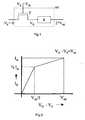
- a typical memory cell with a programmable phase-change resistanceis shown in Figure 12 .
- the source of the (N)MOS-transistor Tis connected to a reference voltage, preferably to common ground, while the drain is connected in series to the programmable resistor R. Accordingly, the transistor conditions may be summarized as follow:
- the gate-source voltage V GS , V GD and V DSare all smaller than V dd , respectively, wherein V dd is the maximum voltage over transistor, e.g. the supply voltage.
- a graph of a simplified NMOS-transistor Tis depicted for a case with a maximum voltage and the gate-source voltage V GS . Therefore, the optimal power dissipation of a programmable resistor in the memory cell will be: P opt ⁇ I m * V dd
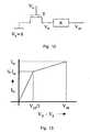
- Figure 1shows the circuit diagram of the basic phase-change memory cell according to the first embodiment.
- the optimal power dissipation of the programmable resistor in the memory cellmay be obtained if the value of the programmable resistor R is selected such that V d - V s corresponds to approximately V dd /3.
- a programmable phase-change resistant Ris connected on its one side to the drain terminal of a NMOS-transistor T and at its other side a voltage of 2*V dd is applied to the programmable resistance R.
- V D2 * V dd - I D * R ⁇ V dd
- FIG. 2shows a graph of the simplified analytical model of the NMOS-transistor of Figure 1 .
- the gate source voltage V GSequals to V dd (max.).
- the optimal power dissipation of the resistor Rcan be achieved if the value of the resistance R is such that V D -V S is about V dd /3.
- a power gain of a factor of 2.5may be achieved by implementing the concept according to the first embodiment.
- FIG 3shows a circuit diagram of an array of phase-change memory cells MC of Figure 1 .
- Each memory cell MCcomprises of a NMOS-transistor T with a programmable phase-change resistor R connected to the drain terminals of the NMOS-transistors T.
- the gates of the NMOS-transistorsare connected to the word-lines wl and the source thereof is connected to the bit-lines bl.
- the programmable phase-change resistor Ris further connected to an action-line al, i.e. the drains of the transistor T is connected via the resistor R to the action line al.
- the action-line alare arranged in parallel with the word-lines wl.
- the RESET-situationis shown.
- Figure 3shows the addressing of the central memory cell CMC within the memory array. All other memory cells MC are not supplied with current. Only the word-line wl of the central cell CMC is supplied with V dd while the other word-lines are supplied with zero voltage. The bit-line bl of the central cell CMC is supplied with zero voltage while the bit-lines of the other cells are supplied with V dd . The action-line al associated to the central cell is supplied with 2*V dd while the other two action-lines al are supplied with V dd .
- the gate source voltage V GS , the gate drain voltage V GD and the drain source voltage V DSare smaller than Vdd, respectively.
- an array of memory cells MCwhich comprise NMOS-transistors operating with a voltage ⁇ V dd , to provide a higher potential difference over the programmable phase-change resistor R, and which comprise an additional action-line al.
- Figure 4shows a circuit diagram of an array of phase-change memory cells MC according to a second embodiment.
- the basic arrangement of the array of memory cells according to the second embodimentcorrespond to the arrangement of the first embodiment.
- a reading operation of a phase-change memory cellscan be performed by supplying V dd to all action-lines al and by applying a read potential of 0 ⁇ V READ ⁇ (V dd -V T ) to one or more of the bit-lines.
- V Tis the threshold value of the transistor.
- the word-line wl associated to the central cell CMCis supplied with V dd while the other two word-lines wl are supplied with zero voltage. All action-lines al are each supplied with V dd while only the bit-line bl associated to the central cell is supplied with V READ . The other bit-lines bl are supplied with V dd . Parallel reading along the same word-line is also possible.
- the programming operationis performed by setting the potential of the bit-line bl to zero for the RESET operation or by setting the potential to V SET , i.e. the SET operation.
- the voltage of the respective action-line alis set to 2*V dd .
- a SET operationcan be performed by using a third potential on the selected action-line. Such potential should be in the range of V dd to 2V dd .
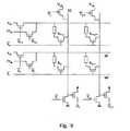
- Figure 5 to Figure 8show circuit diagrams of an array of phase-change memory cells MC according to a third embodiment in order to illustrate the programming thereof.
- the bottom right cell MC1is selected.
- Figure 5shows a circuit diagram of an array of for phase-change memory cells in a reference state, i.e. the bit-lines as well as the action-lines al are supplied with V dd respectively.
- the word-lines wlare supplied with zero voltage.
- Figure 6shows the arrangement of Figure 5 with an adjusted word-line wl, i.e. the second word-line wl is now supplied with V dd instead of zero voltage.
- Figure 7shows the array of Figure 6 with an adjusted action-line al, i.e. the second action-line al is supplied with a voltage of 2V dd .
- Figure 8show the array of Figure 7 with a selected bit-line bl, i.e. the second bit-line bl is either zero voltage or V SET .
- the programming sequencestarts by selecting the word-line wl and thereafter the action-line al.
- the word-line wlmust be selected firstly, i.e. before the action-line al, in order to prevent a high potential difference of larger than V dd over the NMOS-transistor T.
- the bit-lineis selected such that a current will only flow in a state as shown in Figure 8 .
- a parallel programmingis also possible and may be performed by selecting multiple bit-lines in parallel.
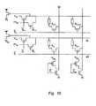
- Figure 9shows a circuit diagram of an array of phase-change memory cells according to a fourth embodiment based on the first, second or third embodiment.
- the RESET, the SET and the READ operationare performed by changing the voltage on the bit-line.
- the reading circuitryis also connected to the bit-line.
- the programming of a selected cellis performed according to the following tables: wl/al S i G i W i WRITE V dd 2 V dd 0 READ V dd 0 2 V dd Not selected 0 0 2 V dd bl V j P j RESET V dd V dd SET V dd V 1 READ V dd V 2 Not selected 0 0
- 0 ⁇ V 1 ⁇ V ddand 0 ⁇ V 2 ⁇ V dd .
- the SET and RESET operationis controlled via the voltage of the bit-line.
- Fig. 10shows a circuit diagram of an array of phase-change memory cells according to a fifth embodiment based on the first, second or third embodiment.
- the RESET and the SET operationis performed on the action-line.
- the action-lineis in parallel to the word-line, no parallel programming or reading is possible for this embodiment.
- the programming of a selected cellis performed according to the following tables: wl/al S i G i W i P j RESET V dd 2 V dd 0 V dd SET V dd 2V dd V l V dd READ V dd 0 2 V dd V dd Not selected 0 0 2V dd 0
- 0 ⁇ V i ⁇ 2 V dd - V T.
- the SET and RESET operationis controlled via the voltage of the action-line.
- the voltage of the bit-line bl as well as the voltage on the action-lineare changed to perform the SET and RESET operation.
- thiswill lead to an increase in the signaling as compared to the fourth and fifth embodiment.
- action-lines alare arranged in parallel to the word-lines wl and orthogonal to the bit-lines.
- programmable resistoris described as a phase-change resistor
- other programmable resistor memoriesmay be implemented with the above principles.
- Such memory cellsmay comprise programmable metallization cells as described in US 5,896,312 or by ferro-electric programmable resistors as described in WO 2004/019410 .
- a factor of 2.5 more powercan be delivered to the phase-change resistor in the phase-change memory cell without increasing the size of the NMOS-transistor.
- the selected cellis supplied with a voltage which is higher than V dd , preferably 2V dd , wherein V dd is the maximum allowable source-drain voltage. Even though a higher voltage is applied to the selected cell the voltage over the selection element will remain below V dd because of the voltage drop over the programmable phase-change resistor connected to the drain of the transistor.
- the current through the other non-conducting, non-selected phase-change memory cellsis maintained at zero, while the voltage over the programmable resistor is increased with reference to the prior art programmable resistor.
Landscapes
- Chemical & Material Sciences (AREA)
- Crystallography & Structural Chemistry (AREA)
- Semiconductor Memories (AREA)
- Read Only Memory (AREA)
- Techniques For Improving Reliability Of Storages (AREA)
Abstract
Description
- The present invention relates to an integrated circuit with memory cells comprising a programmable resistor as well as a method for accessing memory cells comprising a programmable resistor.
- New semiconductor memory devices which are based on the use of so-called phase-change materials as data storage mechanism, i.e. phase-change memories, may become the non-volatile memories of the next generation. The phase-change memories explore the reversible changes in the crystal structure for example of chalcogenide alloys.
- The phase-change memory typically comprise an array of constituent cells wherein each cell has some phase-change material for storing data. By incorporating the chalcogenide alloy into an integrated circuit such a cell may act as fast switching programmable resistor. In particular, such a phase-change memory cell comprises a series arrangement of a resistor composed of phase-change material and some kind of selection means. The phase-change material is characterized by a low ohmic crystalline state and a high ohmic amorphous state. The amorphous state has the property that above a certain threshold voltage low ohmic filaments are formed. In this way enough power can be dissipated in the SET pulse to switch to the crystalline state.
- The change from the crystalline to the amorphous phase of the phase-change material can be programmed with a short high power pulse, i.e. RESET. The change from amorphous to crystalline state is performed by programming the material with a relative longer and lower power pulse, i.e. SET. For more details on programming a phase-change material memory please refer to
WO 2004/025659 A1 . - The selection means may be implemented as a diode, bipolar transistor or a (N)MOS-transistor. Regarding embedded applications the usage of a NMOS-transistor in series with the programmable phase-change resistor is the preferable option in terms of the fabrication and because it is the most reliable option for embedded applications.
- A memory based on an array of NMOS-transistor with programmable resistor according to the prior art is shown in
Figure 11 . The drains of the respective transistors are connected via the programmable resistor to the bit-line b1. The gates of the NMOS-transistors are connected to the word-lines wl. The source of the transistor is connected to common ground. Here, an implementation of addressing merely the central cell for a RESET operation by applying Vdd to the word-line wl and the bit-line bl for the central cell is shown. All other word lines and bit-lines are addressed with zero current. Here, RESET is considered as it requires the maximum power to be delivered to the programmable resistor. Another prior art phase-change memory is shown inEP 1326254 and inWO 2004/057618 - A typical memory cell with a programmable phase-change resistance is shown in
Figure 12 . The source of the (N)MOS-transistor T is connected to a reference voltage, preferably to common ground, while the drain is connected in series to the programmable resistor R. Accordingly, the transistor conditions may be summarized as follow: The gate-source voltage VGS, VGD and VDS are all smaller than Vdd, respectively, wherein Vdd is the maximum voltage over transistor, e.g. the supply voltage. - In
Fig. 13 a graph of a simplified NMOS-transistor T is depicted for a case with a maximum voltage and the gate-source voltage VGS. Therefore, the optimal power dissipation of a programmable resistor in the memory cell will be:
- However the usage of a normal size (N)MOS-transistor may not provide sufficient power per transistor-size, which is to be applied to the programmable phase-change resistor. Accordingly, the size of the (N)MOS-transistors has to be increased in order to deliver the required power.
US -6-314-014 discloses a circuit as indicated by the preamble ofclaim 1. - It is therefore an object of the invention to provide an integrated circuit with memory cells comprising a programmable resistor as well as a method of addressing memory cells comprising a programmable resistor which are capable of increasing the available power which can be delivered to a memory cell.
- This object is solved by an integrated circuit according to
claim 1 as well as a method of addressing a memory cell according to claim 7. - These and other aspects of the invention are apparent from and will be elucidated with reference to the embodiment described hereinafter.
Fig. 1 shows a circuit diagram of a basic phase-change memory cell according to a first embodiment;Fig. 2 shows a graph of the simplified model of the NMOS-transistor ofFigure 1 ;Fig. 3 shows the circuit diagram of an array of memory cells ofFigure 1 according to the first embodiment;Fig. 4 shows a circuit diagram of an array of memory cells according to a second embodiment;Fig. 5 shows a circuit diagram of an array of memory cells according to a third embodiment;Fig. 6-8 shows a circuit diagram of an array of phase-change memory sells for illustrating the programming of the array, respectively;Fig. 9 shows a circuit diagram of an array of phase-change memory cells according to a fourth embodiment;Fig. 10 shows a circuit diagram of an array of phase-change memory cells according to a fifth embodiment;Fig. 11 shows a circuit diagram of an array of phase-change memory cells according to the prior art;Fig. 12 shows a circuit diagram of a phase-change memory cell according to the prior art; andFig. 13 shows a graph of a simplified NMOS-transistor model according toFig. 12 .Figure 1 shows the circuit diagram of the basic phase-change memory cell according to the first embodiment. The optimal power dissipation of the programmable resistor in the memory cell may be obtained if the value of the programmable resistor R is selected such that Vd - Vs corresponds to approximately Vdd/3.
Hence,


- A programmable phase-change resistant R is connected on its one side to the drain terminal of a NMOS-transistor T and at its other side a voltage of 2*Vdd is applied to the programmable resistance R. A voltage of Vdd is applied to the drain terminal of the NMOS-transistor T while the source terminal is connected to common ground Vs=0.
- The value of the resistance R must be designed such that the following equation is met:

Figure 2 shows a graph of the simplified analytical model of the NMOS-transistor ofFigure 1 . Here, the gate source voltage VGS equals to Vdd (max.). In this case the optimal power dissipation of the resistor R can be achieved if the value of the resistance R is such that VD-VS is about Vdd/3.
Hence,

- Accordingly, a power gain of a factor of 2.5 may be achieved by implementing the concept according to the first embodiment.
Figure 3 shows a circuit diagram of an array of phase-change memory cells MC ofFigure 1 . Each memory cell MC comprises of a NMOS-transistor T with a programmable phase-change resistor R connected to the drain terminals of the NMOS-transistors T. The gates of the NMOS-transistors are connected to the word-lines wl and the source thereof is connected to the bit-lines bl. The programmable phase-change resistor R is further connected to an action-line al, i.e. the drains of the transistor T is connected via the resistor R to the action line al. The action-line al are arranged in parallel with the word-lines wl. Here, the RESET-situation is shown.- In particular,
Figure 3 shows the addressing of the central memory cell CMC within the memory array. All other memory cells MC are not supplied with current. Only the word-line wl of the central cell CMC is supplied with Vdd while the other word-lines are supplied with zero voltage. The bit-line bl of the central cell CMC is supplied with zero voltage while the bit-lines of the other cells are supplied with Vdd. The action-line al associated to the central cell is supplied with 2*Vdd while the other two action-lines al are supplied with Vdd. - All necessary transistor conditions will be maintained as long as the resistor comprises the values as shown with regard to
Figure 2 . Accordingly, the gate source voltage VGS, the gate drain voltage VGD and the drain source voltage VDS are smaller than Vdd, respectively. - Accordingly, an array of memory cells MC is shown which comprise NMOS-transistors operating with a voltage ≤ Vdd, to provide a higher potential difference over the programmable phase-change resistor R, and which comprise an additional action-line al.
Figure 4 shows a circuit diagram of an array of phase-change memory cells MC according to a second embodiment. The basic arrangement of the array of memory cells according to the second embodiment correspond to the arrangement of the first embodiment. A reading operation of a phase-change memory cells can be performed by supplying Vdd to all action-lines al and by applying a read potential of 0 < VREAD < (Vdd-VT) to one or more of the bit-lines. As usual, the bit-lines bl are connected to typical sense amplifies for sensing. VT is the threshold value of the transistor.- Here, the word-line wl associated to the central cell CMC is supplied with Vdd while the other two word-lines wl are supplied with zero voltage. All action-lines al are each supplied with Vdd while only the bit-line bl associated to the central cell is supplied with VREAD. The other bit-lines bl are supplied with Vdd. Parallel reading along the same word-line is also possible.
- The programming operation is performed by setting the potential of the bit-line bl to zero for the RESET operation or by setting the potential to VSET, i.e. the SET operation. The voltage of the respective action-line al is set to 2*Vdd. Please note that several bit-lines bl may be programmed in parallel in this way. Alternatively, a SET operation can be performed by using a third potential on the selected action-line. Such potential should be in the range of Vdd to 2Vdd. Here, it is possible to program multiple cells along the selected action-line (and word-line) in parallel.
Figure 5 to Figure 8 show circuit diagrams of an array of phase-change memory cells MC according to a third embodiment in order to illustrate the programming thereof. Here, the bottom right cell MC1 is selected.Figure 5 shows a circuit diagram of an array of for phase-change memory cells in a reference state, i.e. the bit-lines as well as the action-lines al are supplied with Vdd respectively. The word-lines wl are supplied with zero voltage.Figure 6 shows the arrangement ofFigure 5 with an adjusted word-line wl, i.e. the second word-line wl is now supplied with Vdd instead of zero voltage.Figure 7 shows the array ofFigure 6 with an adjusted action-line al, i.e. the second action-line al is supplied with a voltage of 2Vdd.Figure 8 show the array ofFigure 7 with a selected bit-line bl, i.e. the second bit-line bl is either zero voltage or VSET.- Accordingly, the programming sequence starts by selecting the word-line wl and thereafter the action-line al. The word-line wl must be selected firstly, i.e. before the action-line al, in order to prevent a high potential difference of larger than Vdd over the NMOS-transistor T. Finally, the bit-line is selected such that a current will only flow in a state as shown in
Figure 8 . A parallel programming is also possible and may be performed by selecting multiple bit-lines in parallel. Figure 9 shows a circuit diagram of an array of phase-change memory cells according to a fourth embodiment based on the first, second or third embodiment. Here, the RESET, the SET and the READ operation are performed by changing the voltage on the bit-line. The reading circuitry is also connected to the bit-line.- The programming of a selected cell is performed according to the following tables:
wl/al Si Gi Wi WRITE Vdd 2 V dd0 READ V dd 0 2 Vdd Not selected 0 0 2 Vdd bl Vj Pj RESET Vdd Vdd SET Vdd V1 READ Vdd V2 Not selected 0 0 Fig. 10 shows a circuit diagram of an array of phase-change memory cells according to a fifth embodiment based on the first, second or third embodiment. Here, the RESET and the SET operation is performed on the action-line. As the action-line is in parallel to the word-line, no parallel programming or reading is possible for this embodiment.- The programming of a selected cell is performed according to the following tables:
wl/al Si Gi Wi Pj RESET Vdd 2 Vdd 0 Vdd SET Vdd 2Vdd Vl Vdd READ Vdd 0 2 Vdd Vdd Not selected 0 0 2V dd0 - Alternatively, to the fourth and fifth embodiment the voltage of the bit-line bl as well as the voltage on the action-line are changed to perform the SET and RESET operation. However, this will lead to an increase in the signaling as compared to the fourth and fifth embodiment.
- It should be noted that for all above embodiments the action-lines al are arranged in parallel to the word-lines wl and orthogonal to the bit-lines.
- Although in the above embodiments the programmable resistor is described as a phase-change resistor, also other programmable resistor memories may be implemented with the above principles. Such memory cells may comprise programmable metallization cells as described in
US 5,896,312 or by ferro-electric programmable resistors as described inWO 2004/019410 . - Summarizing it can be said, that by introducing a third line, namely the action-line which is connected via the programmable phase-change resistor to the drain-terminal of the NMOS-transistors in combination with an improved addressing technique, a factor of 2.5 more power can be delivered to the phase-change resistor in the phase-change memory cell without increasing the size of the NMOS-transistor. The selected cell is supplied with a voltage which is higher than Vdd, preferably 2Vdd, wherein Vdd is the maximum allowable source-drain voltage. Even though a higher voltage is applied to the selected cell the voltage over the selection element will remain below Vdd because of the voltage drop over the programmable phase-change resistor connected to the drain of the transistor. The current through the other non-conducting, non-selected phase-change memory cells is maintained at zero, while the voltage over the programmable resistor is increased with reference to the prior art programmable resistor.
- It should be noted that the above-mentioned embodiments illustrate rather than limit the invention, and that those skilled in the art will be able to design many alternative embodiments without departing from the scope of the appended claims. In the claims, any reference signs placed between parentheses shall not be construed as limiting the claim. The word "comprising" does not exclude the presence of elements or steps other than those listed in a claim. The word "a" or "an" preceding an element does not exclude the presence of a plurality of such elements. In the device claim enumerating several means, several of these means can be embodied by one and the same item of hardware. The mere fact that certain measures are recited in mutually different dependent claims does not indicate that a combination of these measures cannot be used to advantage.
- Furthermore, any reference signs in the claims shall not be construed as limiting the scope of the claims.


Claims (7)
- Integrated circuit, comprising
a plurality of bit-lines (bl) and a plurality of word-lines (wl) as well as a plurality of memory cells (MC) coupled between a separate bit-line/word-line pair of the plurality of bit-lines (bl) and word-lines (wl) for storing data in the memory cell (MC),
wherein each memory cell (MC) comprises a selecting unit (T) and a programmable resistor (R), and
a further addressing line (al) connected to the memory cell (MC), wherein said selecting unit (T) is implemented as a NMOS-transistor (T), with its gate connected to the respective word-line (wl), and with its source connected to the respective bit-line (bl),
wherein the programmable resistance (R) is connected between the drain of the transistor (T), and the further addressing-line (al),characterized in that the integrated circuit is adapted to select the word-line (wl) before the further addressing-line (al). - Integrated circuit according to claim 1, wherein said programmable resistor (R) is a programmable phase change resistor (R).
- Integrated circuit according to claim 1 or 2, wherein the further addressing-line (al) is connected in parallel to the word-line (wl) and orthogonal to the bit-line (bl).
- Integrated circuit according to claim 1 - 3, wherein a high voltage is applied to the gate of the transistor of the selected memory cell, and wherein said further addressing-line (al) is supplied with a voltage larger than said high voltage and smaller than or equal to 2 times said high voltage in order to program (SET, RESET) a selected memory cell.
- Integrated circuit according to claim 1 or 2,
wherein all further addressing-lines (al) are supplied with a first voltage while a second voltage is supplied to at least one bit-line (bl) for reading a memory cell,
wherein the first voltage is higher than the second voltage. - Integrated circuit according to claim 1,
wherein the word-line (wl) and the further addressing line (al) are selected before the bit-line (bl). - Method for addressing a memory cell within an array of memory cells with bit-lines (bl) and word-lines (wl), wherein each memory cell comprises a selecting unit (T) and a programmable resistance (R), and a further addressing line (al) connected to the memory cell (MC), wherein said selecting unit (T) is implemented as a NMOS-transistor (T), with its gate connected to the respective word-line (wl), and with its source connected to the respective bit-line (bl), wherein the programmable resistance (R) is connected between the drain of the transistor (T), and the further addressing-line (al), the method comprising the step of:• addressing said memory cell through the further addressing-line (al), the method being•characterized in that the word-line (wl) is selected before the further addressing-line (al).
Priority Applications (1)
| Application Number | Priority Date | Filing Date | Title |
|---|---|---|---|
| EP05790410AEP1797566B1 (en) | 2004-09-30 | 2005-08-19 | Integrated circuit with memory cells comprising a programmable resistor and method for addressing memory cells comprising a programmable resistor |
Applications Claiming Priority (3)
| Application Number | Priority Date | Filing Date | Title |
|---|---|---|---|
| EP04104797 | 2004-09-30 | ||
| PCT/IB2005/052730WO2006035326A1 (en) | 2004-09-30 | 2005-08-19 | Integrated circuit with memory cells comprising a programmable resistor and method for addressing memory cells comprising a programmable resistor |
| EP05790410AEP1797566B1 (en) | 2004-09-30 | 2005-08-19 | Integrated circuit with memory cells comprising a programmable resistor and method for addressing memory cells comprising a programmable resistor |
Publications (2)
| Publication Number | Publication Date |
|---|---|
| EP1797566A1 EP1797566A1 (en) | 2007-06-20 |
| EP1797566B1true EP1797566B1 (en) | 2010-11-17 |
Family
ID=35457343
Family Applications (1)
| Application Number | Title | Priority Date | Filing Date |
|---|---|---|---|
| EP05790410AExpired - LifetimeEP1797566B1 (en) | 2004-09-30 | 2005-08-19 | Integrated circuit with memory cells comprising a programmable resistor and method for addressing memory cells comprising a programmable resistor |
Country Status (7)
| Country | Link |
|---|---|
| US (1) | US8335103B2 (en) |
| EP (1) | EP1797566B1 (en) |
| JP (1) | JP2008515127A (en) |
| CN (1) | CN100568390C (en) |
| AT (1) | ATE488842T1 (en) |
| DE (1) | DE602005024840D1 (en) |
| WO (1) | WO2006035326A1 (en) |
Families Citing this family (7)
| Publication number | Priority date | Publication date | Assignee | Title |
|---|---|---|---|---|
| US7679980B2 (en)* | 2006-11-21 | 2010-03-16 | Qimonda North America Corp. | Resistive memory including selective refresh operation |
| US20100182044A1 (en)* | 2007-03-13 | 2010-07-22 | Easic Corporation | Programming and circuit topologies for programmable vias |
| WO2009090589A1 (en) | 2008-01-16 | 2009-07-23 | Nxp B.V. | Multilayer structure comprising a phase change material layer and a method of producing the same |
| US8294488B1 (en)* | 2009-04-24 | 2012-10-23 | Adesto Technologies Corporation | Programmable impedance element circuits and methods |
| KR20120098326A (en)* | 2011-02-28 | 2012-09-05 | 에스케이하이닉스 주식회사 | Semiconductor apparatus and method of processing data |
| CN103592883B (en)* | 2013-12-02 | 2016-01-20 | 哈尔滨工业大学 | The accurate programmable resistance module of multichannel based on DSP and control method thereof |
| US11646079B2 (en) | 2020-08-26 | 2023-05-09 | Taiwan Semiconductor Manufacturing Company, Ltd. | Memory cell including programmable resistors with transistor components |
Family Cites Families (22)
| Publication number | Priority date | Publication date | Assignee | Title |
|---|---|---|---|---|
| GB8627488D0 (en) | 1986-11-18 | 1986-12-17 | British Petroleum Co Plc | Memory matrix |
| US5761115A (en)* | 1996-05-30 | 1998-06-02 | Axon Technologies Corporation | Programmable metallization cell structure and method of making same |
| US6314014B1 (en)* | 1999-12-16 | 2001-11-06 | Ovonyx, Inc. | Programmable resistance memory arrays with reference cells |
| JP4667594B2 (en)* | 2000-12-25 | 2011-04-13 | ルネサスエレクトロニクス株式会社 | Thin film magnetic memory device |
| DE60137788D1 (en) | 2001-12-27 | 2009-04-09 | St Microelectronics Srl | Architecture of a non-volatile phase change memory matrix |
| CN100337333C (en)* | 2002-04-10 | 2007-09-12 | 松下电器产业株式会社 | Non-volatile flip-flop |
| JP4282314B2 (en)* | 2002-06-25 | 2009-06-17 | シャープ株式会社 | Storage device |
| JP2005536068A (en) | 2002-08-20 | 2005-11-24 | コーニンクレッカ フィリップス エレクトロニクス エヌ ヴィ | Ferroelectric device and manufacturing method thereof |
| JP4094006B2 (en) | 2002-09-11 | 2008-06-04 | オヴォニクス,インコーポレイテッド | How to program phase change material memory |
| JP2004185755A (en)* | 2002-12-05 | 2004-07-02 | Sharp Corp | Nonvolatile semiconductor memory device |
| JP4124635B2 (en) | 2002-12-05 | 2008-07-23 | シャープ株式会社 | Semiconductor memory device and memory cell array erasing method |
| AU2003283730A1 (en) | 2002-12-19 | 2004-07-14 | Koninklijke Philips Electronics N.V. | Electric device comprising a layer of phase change material and method of manufacturing the same |
| KR100479810B1 (en)* | 2002-12-30 | 2005-03-31 | 주식회사 하이닉스반도체 | Non-volatile memory device |
| JP2004288282A (en)* | 2003-03-20 | 2004-10-14 | Fujitsu Ltd | Semiconductor device |
| JP4254293B2 (en) | 2003-03-25 | 2009-04-15 | 株式会社日立製作所 | Storage device |
| JP4113493B2 (en) | 2003-06-12 | 2008-07-09 | シャープ株式会社 | Nonvolatile semiconductor memory device and control method thereof |
| US7180767B2 (en) | 2003-06-18 | 2007-02-20 | Macronix International Co., Ltd. | Multi-level memory device and methods for programming and reading the same |
| CN1717748A (en) | 2003-06-25 | 2006-01-04 | 松下电器产业株式会社 | Method of driving non-volatile memory |
| JP4356542B2 (en)* | 2003-08-27 | 2009-11-04 | 日本電気株式会社 | Semiconductor device |
| DE10353641B4 (en) | 2003-11-17 | 2016-12-01 | Robert Bosch Gmbh | Fuel injector |
| JP2005183619A (en)* | 2003-12-18 | 2005-07-07 | Canon Inc | Non-volatile memory device |
| JP4646636B2 (en)* | 2004-02-20 | 2011-03-09 | ルネサスエレクトロニクス株式会社 | Semiconductor device |
- 2005
- 2005-08-19EPEP05790410Apatent/EP1797566B1/ennot_activeExpired - Lifetime
- 2005-08-19CNCN200580040979.4Apatent/CN100568390C/ennot_activeExpired - Fee Related
- 2005-08-19DEDE602005024840Tpatent/DE602005024840D1/ennot_activeExpired - Lifetime
- 2005-08-19JPJP2007534117Apatent/JP2008515127A/ennot_activeWithdrawn
- 2005-08-19USUS11/576,459patent/US8335103B2/ennot_activeExpired - Fee Related
- 2005-08-19ATAT05790410Tpatent/ATE488842T1/ennot_activeIP Right Cessation
- 2005-08-19WOPCT/IB2005/052730patent/WO2006035326A1/enactiveApplication Filing
Also Published As
| Publication number | Publication date |
|---|---|
| DE602005024840D1 (en) | 2010-12-30 |
| EP1797566A1 (en) | 2007-06-20 |
| WO2006035326A1 (en) | 2006-04-06 |
| JP2008515127A (en) | 2008-05-08 |
| ATE488842T1 (en) | 2010-12-15 |
| CN100568390C (en) | 2009-12-09 |
| US8335103B2 (en) | 2012-12-18 |
| US20100214827A1 (en) | 2010-08-26 |
| CN101069241A (en) | 2007-11-07 |
Similar Documents
| Publication | Publication Date | Title |
|---|---|---|
| US6928022B2 (en) | Write driver circuit in phase change memory device and method for applying write current | |
| US6462984B1 (en) | Biasing scheme of floating unselected wordlines and bitlines of a diode-based memory array | |
| EP0517354B1 (en) | Semiconductor memory circuit having a test logic circuit structure | |
| US20170352416A1 (en) | Apparatuses, memories, and methods for address decoding and selecting an access line | |
| US20110110142A1 (en) | Memory device and method of reading memory device | |
| US9236123B2 (en) | Semiconductor device and write method | |
| EP0055594B1 (en) | Electrically programmable non-volatile semiconductor memory device | |
| US7474553B2 (en) | Device writing to a plurality of rows in a memory matrix simultaneously | |
| US6414895B2 (en) | Semiconductor memory device with reduced standby current | |
| US20060013058A1 (en) | Phase change memory device for use in a burst read operation and a data reading method thereof | |
| US6985389B2 (en) | Phase change based memory device and method for operating same | |
| EP1797566B1 (en) | Integrated circuit with memory cells comprising a programmable resistor and method for addressing memory cells comprising a programmable resistor | |
| US7869267B2 (en) | Method for low power accessing a phase change memory device | |
| US7327603B2 (en) | Memory device including electrical circuit configured to provide reversible bias across the PMC memory cell to perform erase and write functions | |
| KR102482147B1 (en) | Electrical Fuse OTP Memory | |
| US5390150A (en) | Semiconductor memory device with redundancy structure suppressing power consumption | |
| CN114664346A (en) | Anti-fuse memory array circuit and operation method thereof and memory | |
| JP5208011B2 (en) | Memory circuit device | |
| US7835196B2 (en) | Nonvolatile memory device storing data based on change in transistor characteristics | |
| KR101654418B1 (en) | Memory device with a common source line masking circuit | |
| EP1733398B1 (en) | Circuit for accessing a chalcogenide memory array | |
| US6477102B1 (en) | Redundant programmable circuit and semiconductor memory device having the same | |
| EP1845532A1 (en) | A column decoding system for semiconductor memory devices implemented with low voltage transistors | |
| US8755237B2 (en) | SRAM power reduction through selective programming | |
| US7580275B2 (en) | Control of a memory matrix with resistance hysteresis elements |
Legal Events
| Date | Code | Title | Description |
|---|---|---|---|
| PUAI | Public reference made under article 153(3) epc to a published international application that has entered the european phase | Free format text:ORIGINAL CODE: 0009012 | |
| 17P | Request for examination filed | Effective date:20070502 | |
| AK | Designated contracting states | Kind code of ref document:A1 Designated state(s):AT BE BG CH CY CZ DE DK EE ES FI FR GB GR HU IE IS IT LI LT LU LV MC NL PL PT RO SE SI SK TR | |
| AX | Request for extension of the european patent | Extension state:AL BA HR MK YU | |
| RAP1 | Party data changed (applicant data changed or rights of an application transferred) | Owner name:NXP B.V. | |
| RAP1 | Party data changed (applicant data changed or rights of an application transferred) | Owner name:NXP B.V. | |
| GRAP | Despatch of communication of intention to grant a patent | Free format text:ORIGINAL CODE: EPIDOSNIGR1 | |
| GRAS | Grant fee paid | Free format text:ORIGINAL CODE: EPIDOSNIGR3 | |
| GRAA | (expected) grant | Free format text:ORIGINAL CODE: 0009210 | |
| AK | Designated contracting states | Kind code of ref document:B1 Designated state(s):AT BE BG CH CY CZ DE DK EE ES FI FR GB GR HU IE IS IT LI LT LU LV MC NL PL PT RO SE SI SK TR | |
| AX | Request for extension of the european patent | Extension state:AL BA HR MK YU | |
| REG | Reference to a national code | Ref country code:GB Ref legal event code:FG4D | |
| REG | Reference to a national code | Ref country code:CH Ref legal event code:EP | |
| REG | Reference to a national code | Ref country code:IE Ref legal event code:FG4D | |
| REF | Corresponds to: | Ref document number:602005024840 Country of ref document:DE Date of ref document:20101230 Kind code of ref document:P | |
| REG | Reference to a national code | Ref country code:NL Ref legal event code:VDEP Effective date:20101117 | |
| LTIE | Lt: invalidation of european patent or patent extension | Effective date:20101117 | |
| PG25 | Lapsed in a contracting state [announced via postgrant information from national office to epo] | Ref country code:LT Free format text:LAPSE BECAUSE OF FAILURE TO SUBMIT A TRANSLATION OF THE DESCRIPTION OR TO PAY THE FEE WITHIN THE PRESCRIBED TIME-LIMIT Effective date:20101117 | |
| PG25 | Lapsed in a contracting state [announced via postgrant information from national office to epo] | Ref country code:BG Free format text:LAPSE BECAUSE OF FAILURE TO SUBMIT A TRANSLATION OF THE DESCRIPTION OR TO PAY THE FEE WITHIN THE PRESCRIBED TIME-LIMIT Effective date:20110217 Ref country code:NL Free format text:LAPSE BECAUSE OF FAILURE TO SUBMIT A TRANSLATION OF THE DESCRIPTION OR TO PAY THE FEE WITHIN THE PRESCRIBED TIME-LIMIT Effective date:20101117 Ref country code:PT Free format text:LAPSE BECAUSE OF FAILURE TO SUBMIT A TRANSLATION OF THE DESCRIPTION OR TO PAY THE FEE WITHIN THE PRESCRIBED TIME-LIMIT Effective date:20110317 Ref country code:CY Free format text:LAPSE BECAUSE OF FAILURE TO SUBMIT A TRANSLATION OF THE DESCRIPTION OR TO PAY THE FEE WITHIN THE PRESCRIBED TIME-LIMIT Effective date:20101117 Ref country code:AT Free format text:LAPSE BECAUSE OF FAILURE TO SUBMIT A TRANSLATION OF THE DESCRIPTION OR TO PAY THE FEE WITHIN THE PRESCRIBED TIME-LIMIT Effective date:20101117 Ref country code:SI Free format text:LAPSE BECAUSE OF FAILURE TO SUBMIT A TRANSLATION OF THE DESCRIPTION OR TO PAY THE FEE WITHIN THE PRESCRIBED TIME-LIMIT Effective date:20101117 Ref country code:LV Free format text:LAPSE BECAUSE OF FAILURE TO SUBMIT A TRANSLATION OF THE DESCRIPTION OR TO PAY THE FEE WITHIN THE PRESCRIBED TIME-LIMIT Effective date:20101117 Ref country code:IS Free format text:LAPSE BECAUSE OF FAILURE TO SUBMIT A TRANSLATION OF THE DESCRIPTION OR TO PAY THE FEE WITHIN THE PRESCRIBED TIME-LIMIT Effective date:20110317 Ref country code:FI Free format text:LAPSE BECAUSE OF FAILURE TO SUBMIT A TRANSLATION OF THE DESCRIPTION OR TO PAY THE FEE WITHIN THE PRESCRIBED TIME-LIMIT Effective date:20101117 Ref country code:SE Free format text:LAPSE BECAUSE OF FAILURE TO SUBMIT A TRANSLATION OF THE DESCRIPTION OR TO PAY THE FEE WITHIN THE PRESCRIBED TIME-LIMIT Effective date:20101117 | |
| PG25 | Lapsed in a contracting state [announced via postgrant information from national office to epo] | Ref country code:GR Free format text:LAPSE BECAUSE OF FAILURE TO SUBMIT A TRANSLATION OF THE DESCRIPTION OR TO PAY THE FEE WITHIN THE PRESCRIBED TIME-LIMIT Effective date:20110218 | |
| PG25 | Lapsed in a contracting state [announced via postgrant information from national office to epo] | Ref country code:EE Free format text:LAPSE BECAUSE OF FAILURE TO SUBMIT A TRANSLATION OF THE DESCRIPTION OR TO PAY THE FEE WITHIN THE PRESCRIBED TIME-LIMIT Effective date:20101117 Ref country code:ES Free format text:LAPSE BECAUSE OF FAILURE TO SUBMIT A TRANSLATION OF THE DESCRIPTION OR TO PAY THE FEE WITHIN THE PRESCRIBED TIME-LIMIT Effective date:20110228 Ref country code:CZ Free format text:LAPSE BECAUSE OF FAILURE TO SUBMIT A TRANSLATION OF THE DESCRIPTION OR TO PAY THE FEE WITHIN THE PRESCRIBED TIME-LIMIT Effective date:20101117 Ref country code:BE Free format text:LAPSE BECAUSE OF FAILURE TO SUBMIT A TRANSLATION OF THE DESCRIPTION OR TO PAY THE FEE WITHIN THE PRESCRIBED TIME-LIMIT Effective date:20101117 | |
| PG25 | Lapsed in a contracting state [announced via postgrant information from national office to epo] | Ref country code:SK Free format text:LAPSE BECAUSE OF FAILURE TO SUBMIT A TRANSLATION OF THE DESCRIPTION OR TO PAY THE FEE WITHIN THE PRESCRIBED TIME-LIMIT Effective date:20101117 Ref country code:RO Free format text:LAPSE BECAUSE OF FAILURE TO SUBMIT A TRANSLATION OF THE DESCRIPTION OR TO PAY THE FEE WITHIN THE PRESCRIBED TIME-LIMIT Effective date:20101117 Ref country code:PL Free format text:LAPSE BECAUSE OF FAILURE TO SUBMIT A TRANSLATION OF THE DESCRIPTION OR TO PAY THE FEE WITHIN THE PRESCRIBED TIME-LIMIT Effective date:20101117 Ref country code:DK Free format text:LAPSE BECAUSE OF FAILURE TO SUBMIT A TRANSLATION OF THE DESCRIPTION OR TO PAY THE FEE WITHIN THE PRESCRIBED TIME-LIMIT Effective date:20101117 | |
| PLBE | No opposition filed within time limit | Free format text:ORIGINAL CODE: 0009261 | |
| STAA | Information on the status of an ep patent application or granted ep patent | Free format text:STATUS: NO OPPOSITION FILED WITHIN TIME LIMIT | |
| 26N | No opposition filed | Effective date:20110818 | |
| REG | Reference to a national code | Ref country code:DE Ref legal event code:R097 Ref document number:602005024840 Country of ref document:DE Effective date:20110818 | |
| PG25 | Lapsed in a contracting state [announced via postgrant information from national office to epo] | Ref country code:IT Free format text:LAPSE BECAUSE OF FAILURE TO SUBMIT A TRANSLATION OF THE DESCRIPTION OR TO PAY THE FEE WITHIN THE PRESCRIBED TIME-LIMIT Effective date:20101117 | |
| REG | Reference to a national code | Ref country code:CH Ref legal event code:PL | |
| PG25 | Lapsed in a contracting state [announced via postgrant information from national office to epo] | Ref country code:CH Free format text:LAPSE BECAUSE OF NON-PAYMENT OF DUE FEES Effective date:20110831 Ref country code:LI Free format text:LAPSE BECAUSE OF NON-PAYMENT OF DUE FEES Effective date:20110831 | |
| REG | Reference to a national code | Ref country code:IE Ref legal event code:MM4A | |
| PG25 | Lapsed in a contracting state [announced via postgrant information from national office to epo] | Ref country code:IE Free format text:LAPSE BECAUSE OF NON-PAYMENT OF DUE FEES Effective date:20110819 | |
| PG25 | Lapsed in a contracting state [announced via postgrant information from national office to epo] | Ref country code:LU Free format text:LAPSE BECAUSE OF NON-PAYMENT OF DUE FEES Effective date:20110819 | |
| PG25 | Lapsed in a contracting state [announced via postgrant information from national office to epo] | Ref country code:MC Free format text:LAPSE BECAUSE OF NON-PAYMENT OF DUE FEES Effective date:20110831 | |
| PG25 | Lapsed in a contracting state [announced via postgrant information from national office to epo] | Ref country code:TR Free format text:LAPSE BECAUSE OF FAILURE TO SUBMIT A TRANSLATION OF THE DESCRIPTION OR TO PAY THE FEE WITHIN THE PRESCRIBED TIME-LIMIT Effective date:20101117 | |
| PG25 | Lapsed in a contracting state [announced via postgrant information from national office to epo] | Ref country code:HU Free format text:LAPSE BECAUSE OF FAILURE TO SUBMIT A TRANSLATION OF THE DESCRIPTION OR TO PAY THE FEE WITHIN THE PRESCRIBED TIME-LIMIT Effective date:20101117 | |
| REG | Reference to a national code | Ref country code:FR Ref legal event code:PLFP Year of fee payment:11 | |
| REG | Reference to a national code | Ref country code:FR Ref legal event code:PLFP Year of fee payment:12 | |
| REG | Reference to a national code | Ref country code:FR Ref legal event code:PLFP Year of fee payment:13 | |
| REG | Reference to a national code | Ref country code:FR Ref legal event code:PLFP Year of fee payment:14 | |
| PGFP | Annual fee paid to national office [announced via postgrant information from national office to epo] | Ref country code:GB Payment date:20220721 Year of fee payment:18 Ref country code:DE Payment date:20220616 Year of fee payment:18 | |
| PGFP | Annual fee paid to national office [announced via postgrant information from national office to epo] | Ref country code:FR Payment date:20220721 Year of fee payment:18 | |
| REG | Reference to a national code | Ref country code:DE Ref legal event code:R119 Ref document number:602005024840 Country of ref document:DE | |
| GBPC | Gb: european patent ceased through non-payment of renewal fee | Effective date:20230819 | |
| PG25 | Lapsed in a contracting state [announced via postgrant information from national office to epo] | Ref country code:GB Free format text:LAPSE BECAUSE OF NON-PAYMENT OF DUE FEES Effective date:20230819 | |
| PG25 | Lapsed in a contracting state [announced via postgrant information from national office to epo] | Ref country code:GB Free format text:LAPSE BECAUSE OF NON-PAYMENT OF DUE FEES Effective date:20230819 Ref country code:FR Free format text:LAPSE BECAUSE OF NON-PAYMENT OF DUE FEES Effective date:20230831 Ref country code:DE Free format text:LAPSE BECAUSE OF NON-PAYMENT OF DUE FEES Effective date:20240301 |